Issue Browser
Volume 42, Issue 6,
Jun 2021


J. Semicond.
2021, 42(6): 061801 doi: 10.1088/1674-4926/42/6/061801

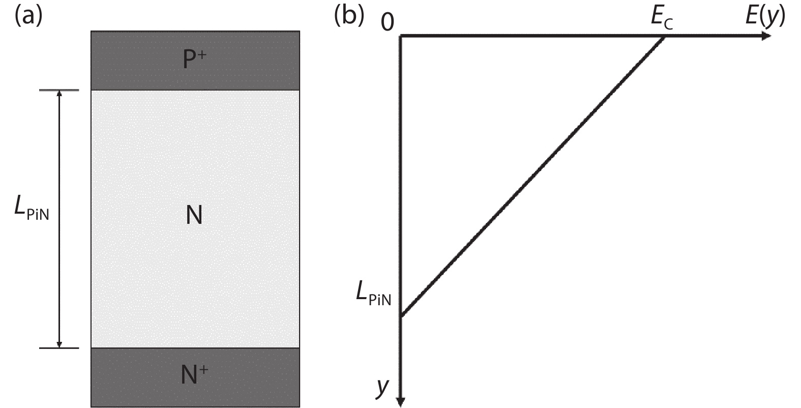
Superjunction technology is believed to reach the optimal specific on-resistance and breakdown voltage trade-off. It has become a mainstream technology in silicon high-voltage metal oxide semiconductor field effect transistor devices. Numerous efforts have been conducted to employ the same concept in silicon carbide devices. These works are summarized here.


J. Semicond.
2021, 42(6): 062301 doi: 10.1088/1674-4926/42/6/062301

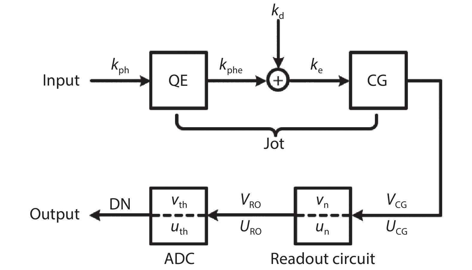
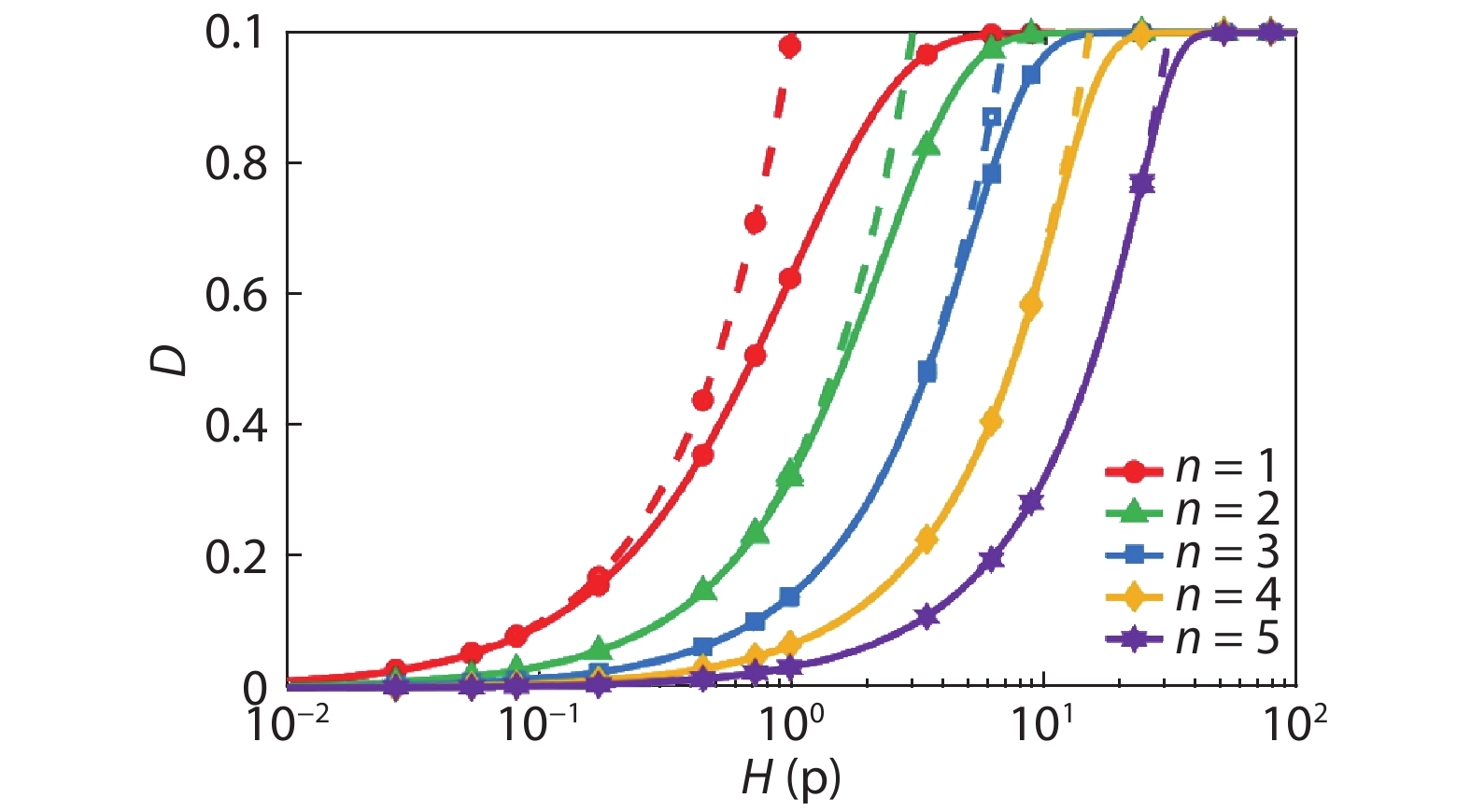
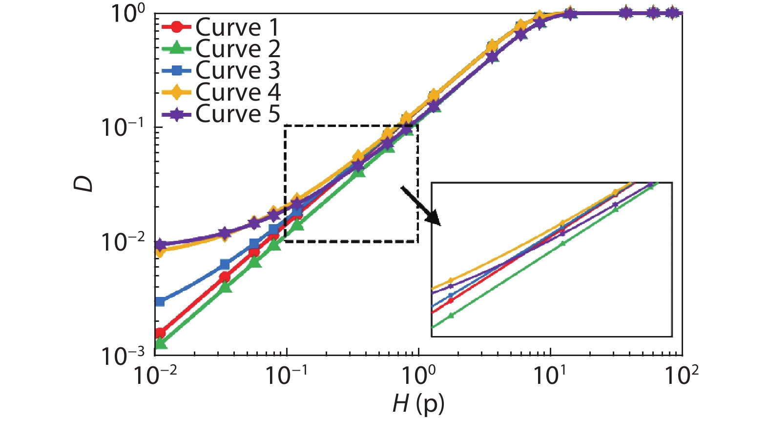
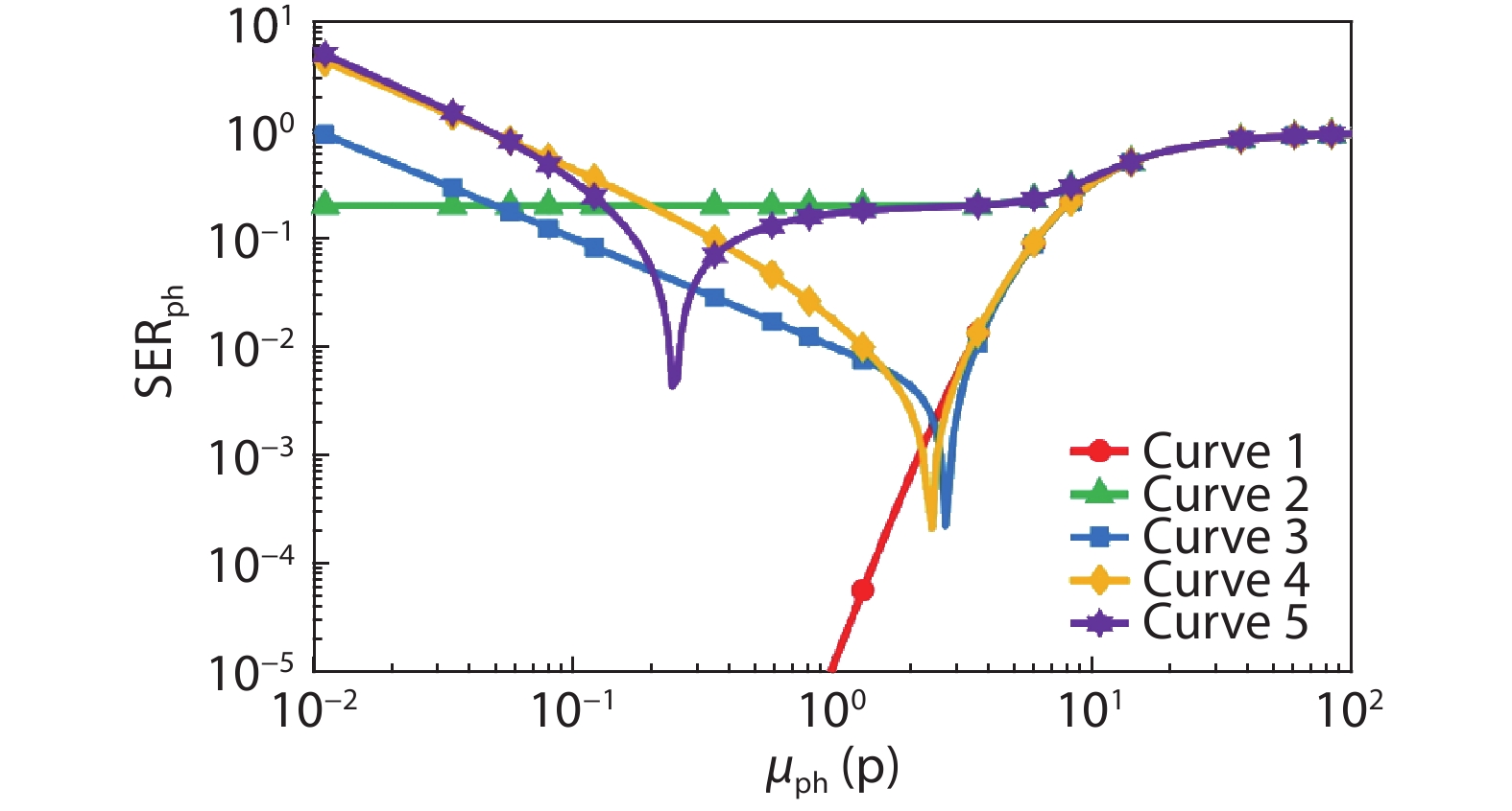
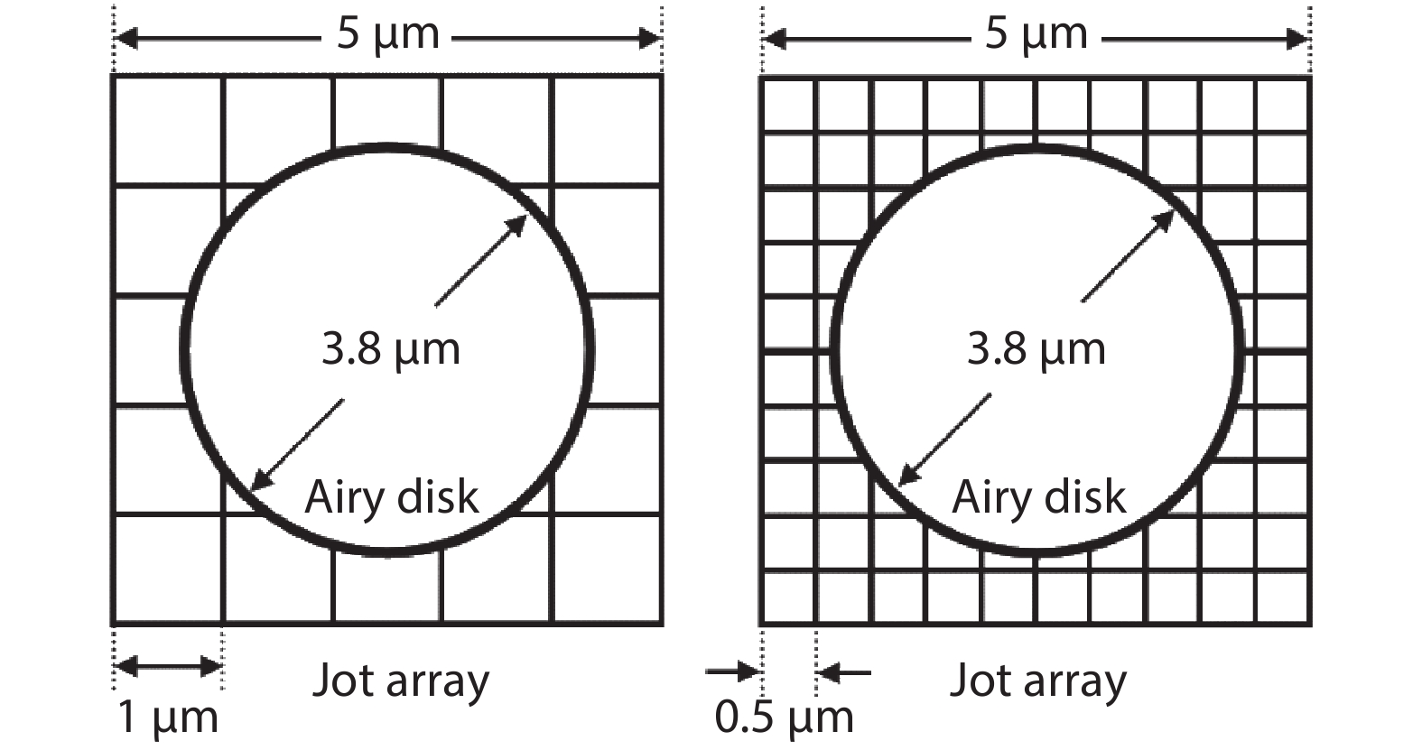
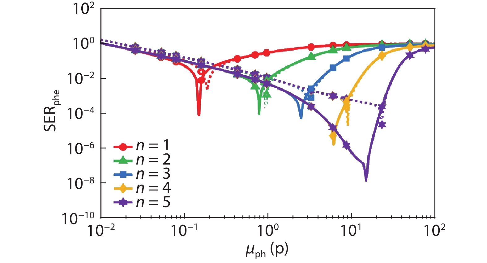
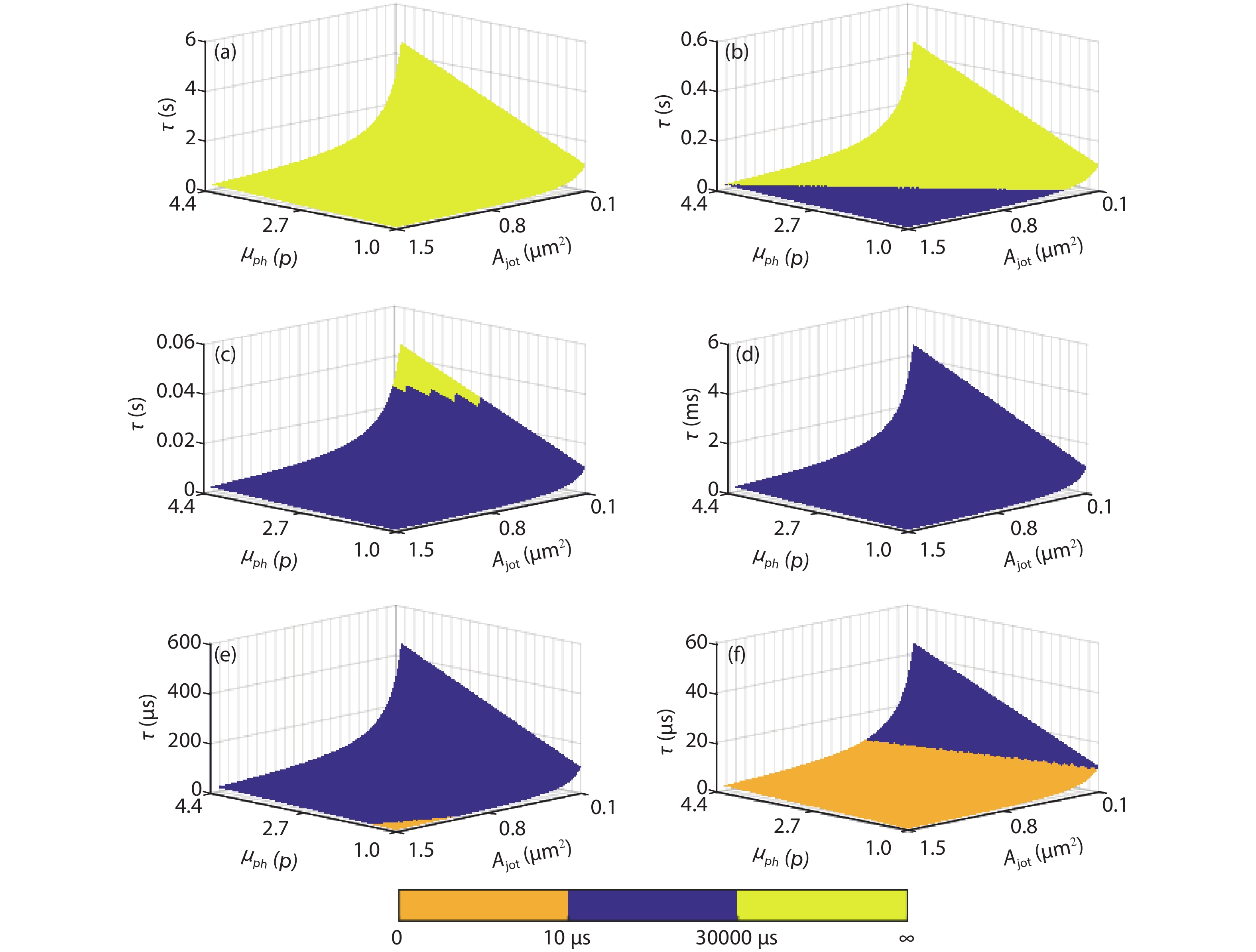
A signal chain model of single-bit and multi-bit quanta image sensors (QISs) is established. Based on the proposed model, the photoresponse characteristics and signal error rates of QISs are investigated, and the effects of bit depth, quantum efficiency, dark current, and read noise on them are analyzed. When the signal error rates towards photons and photoelectrons counting are lower than 0.01, the high accuracy photon and photoelectron counting exposure ranges are determined. Furthermore, an optimization method of integration time to ensure that the QIS works in these high accuracy exposure ranges is presented. The trade-offs between pixel area, the mean value of incident photons, and integration time under different illuminance level are analyzed. For the 3-bit QIS with 0.16 e-/s dark current and 0.21 e- r.m.s. read noise, when the illuminance level and pixel area are 1 lux and 1.21 μm2, or 10 000 lux and 0.21 μm2, the recommended integration time is 8.8 to 30 ms, or 10 to 21.3 μs, respectively. The proposed method can guide the design and operation of single-bit and multi-bit QISs.


J. Semicond.
2021, 42(6): 062302 doi: 10.1088/1674-4926/42/6/062302
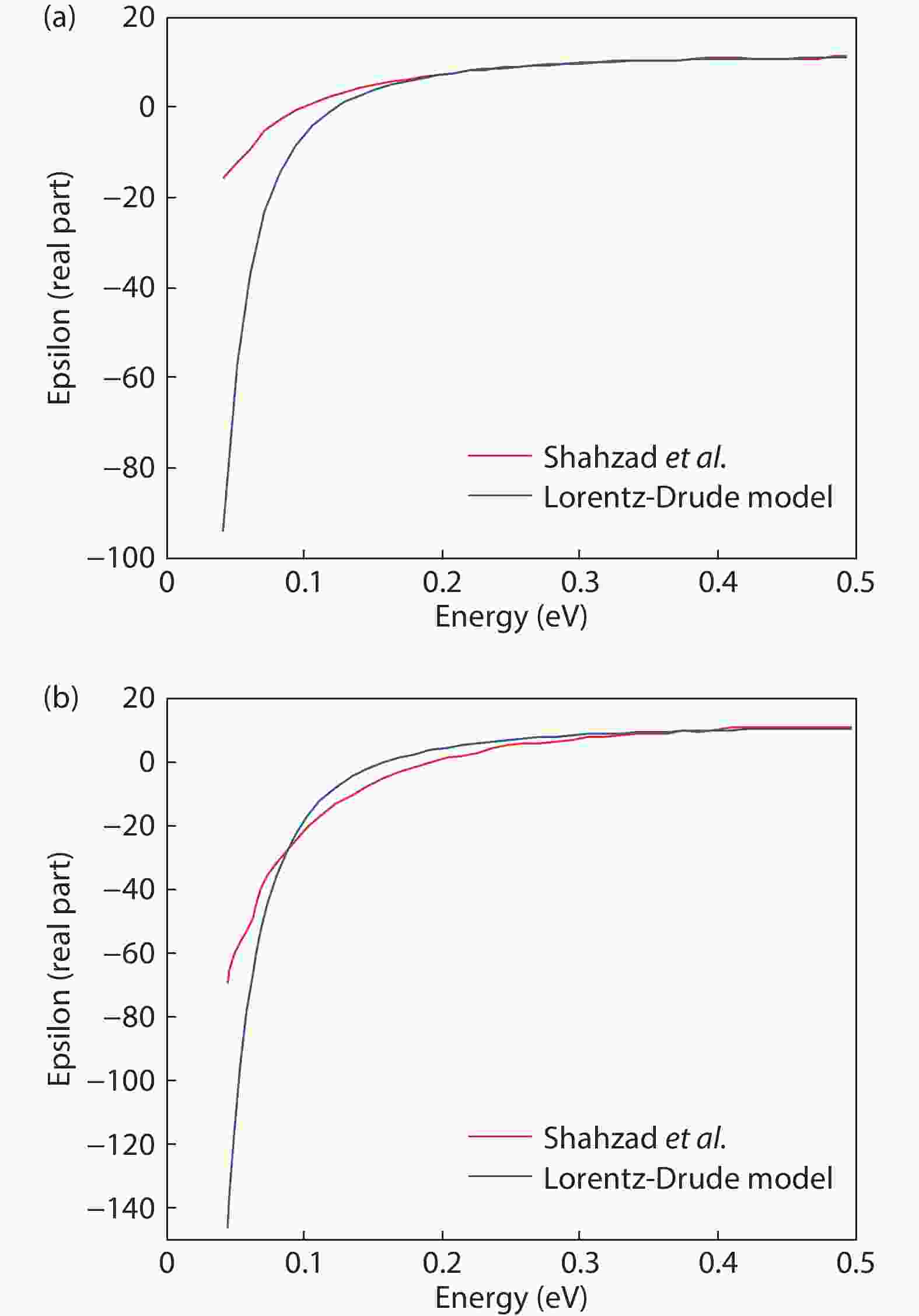
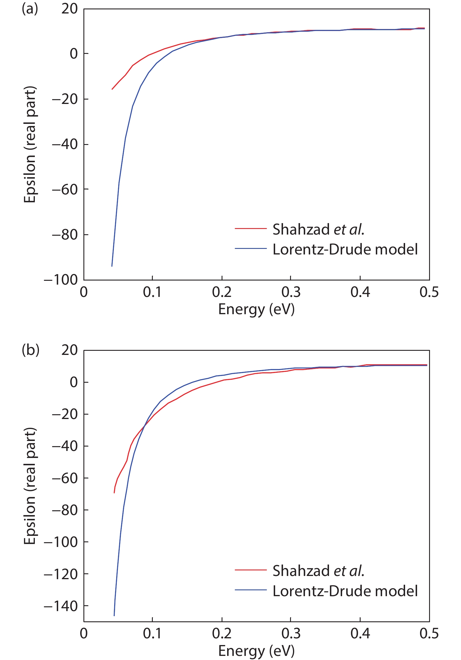
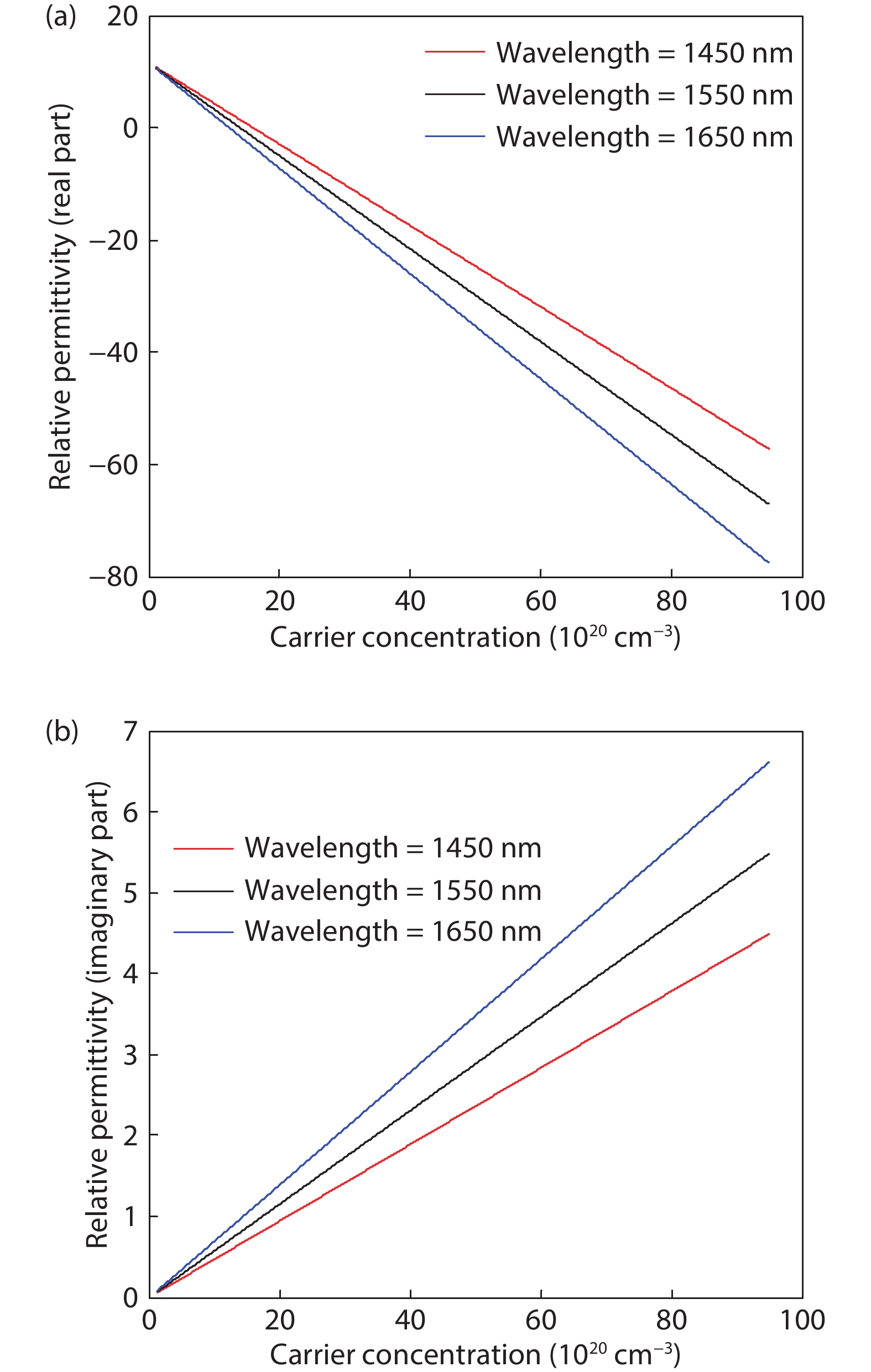
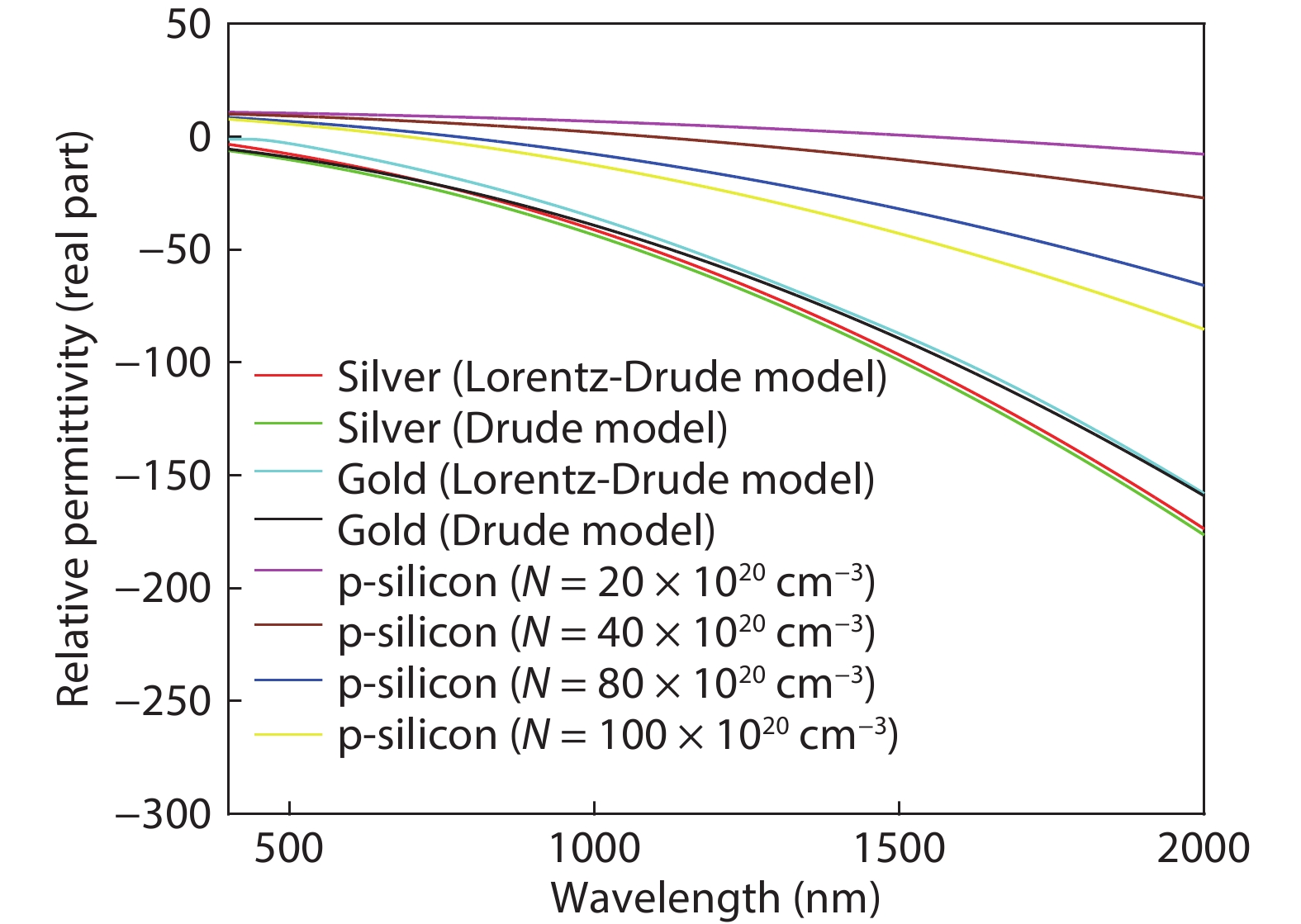
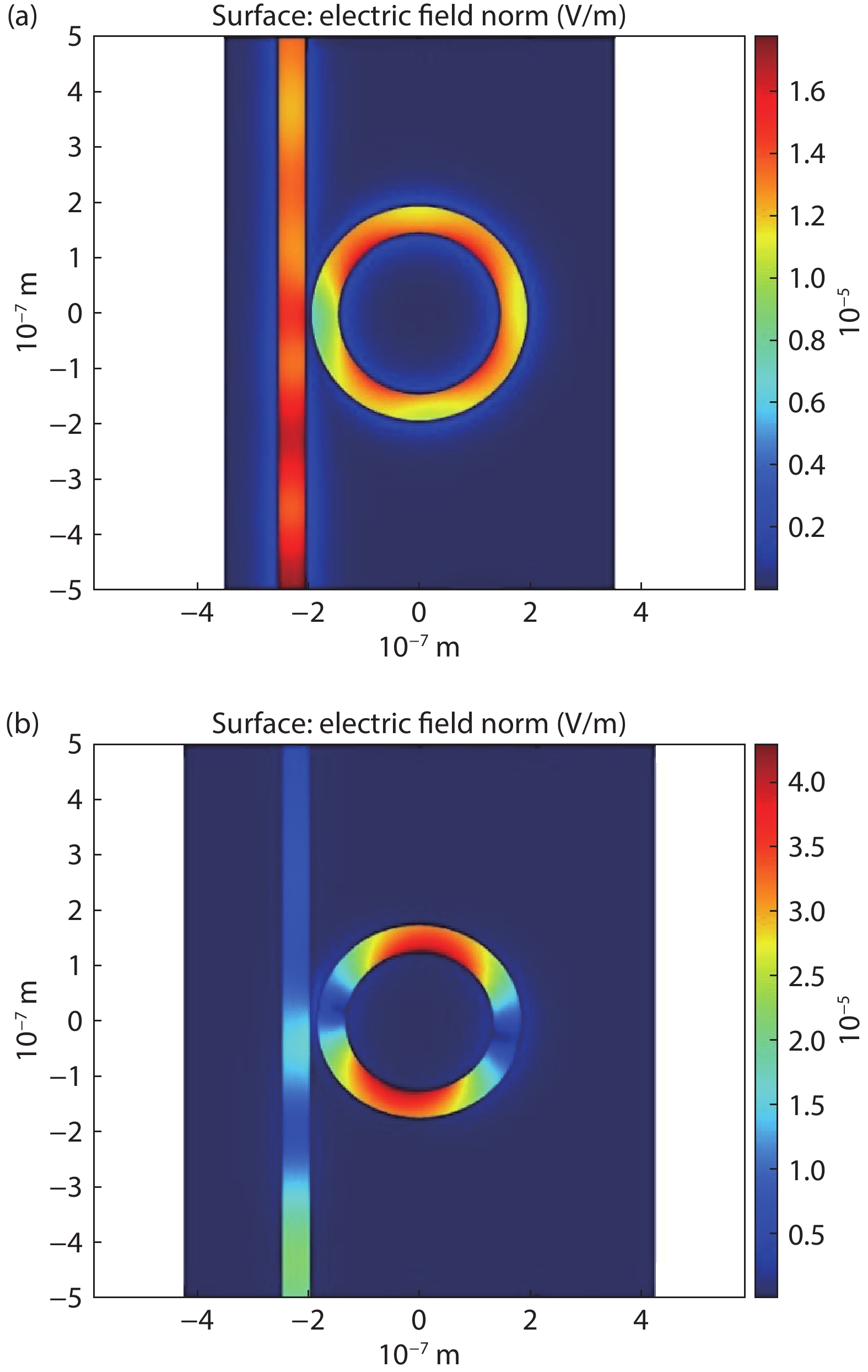
The plasmonic property of heavily doped p-type silicon is studied here. Although most of the plasmonic devices use metal–insulator–metal (MIM) waveguide in order to support the propagation of surface plasmon polaritons (SPPs), metals that possess a number of challenges in loss management, polarization response, nanofabrication etc. On the other hand, heavily doped p-type silicon shows similar plasmonic properties like metals and also enables us to overcome the challenges possessed by metals. For numerical simulation, heavily doped p-silicon is mathematically modeled and the theoretically obtained relative permittivity is compared with the experimental value. A waveguide is formed with the p-silicon-air interface instead of the metal–air interface. Formation and propagation of SPPs similar to MIM waveguides are observed.


J. Semicond.
2021, 42(6): 062801 doi: 10.1088/1674-4926/42/6/062801

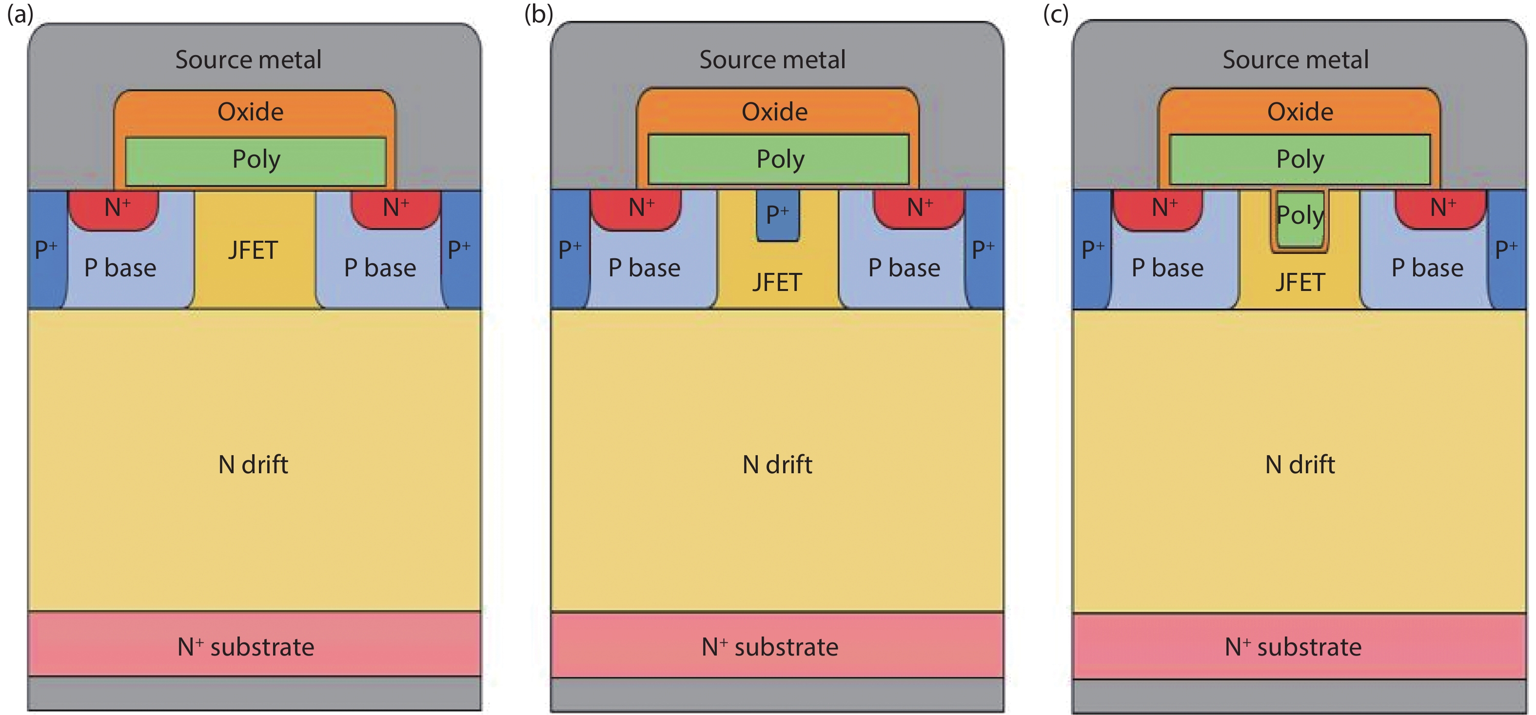
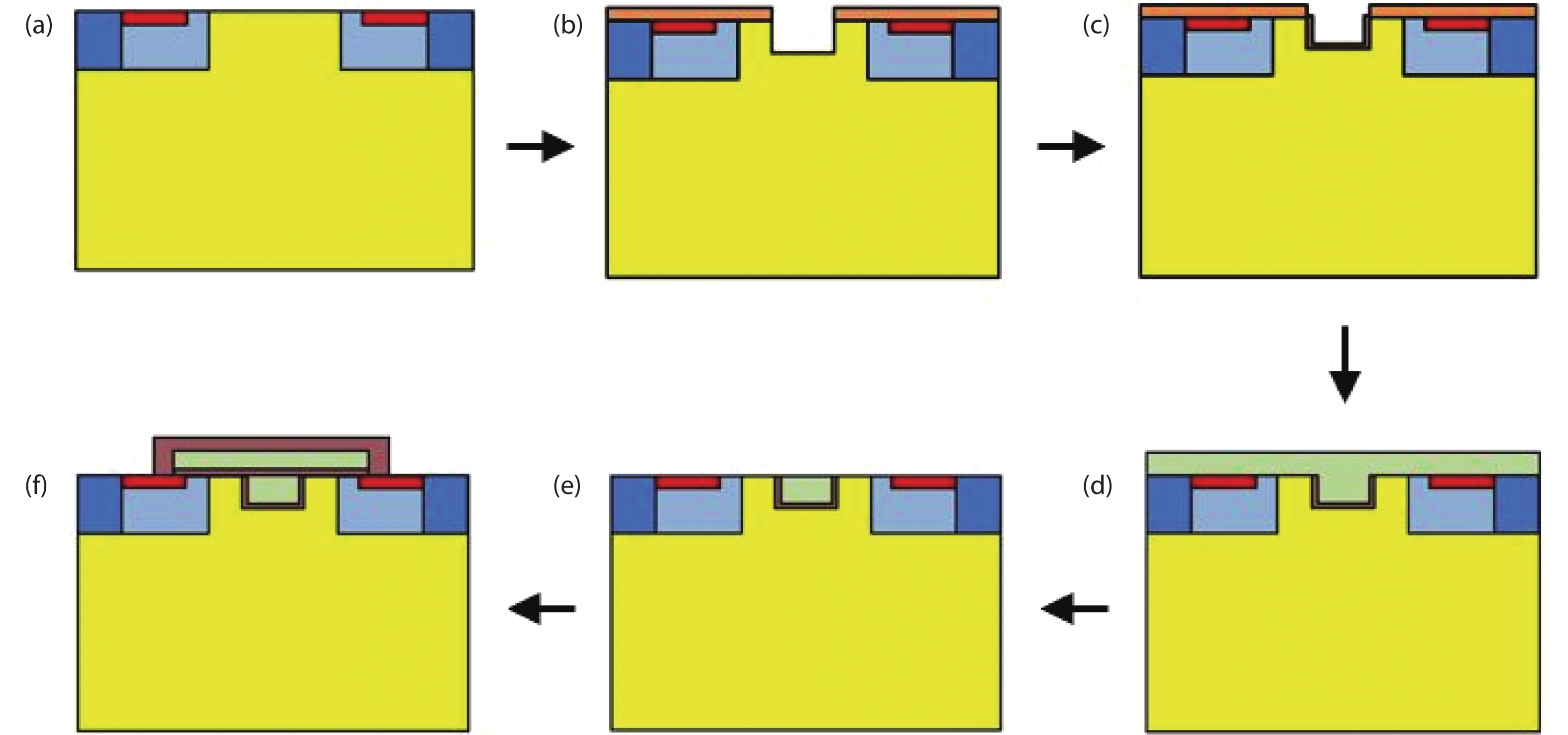
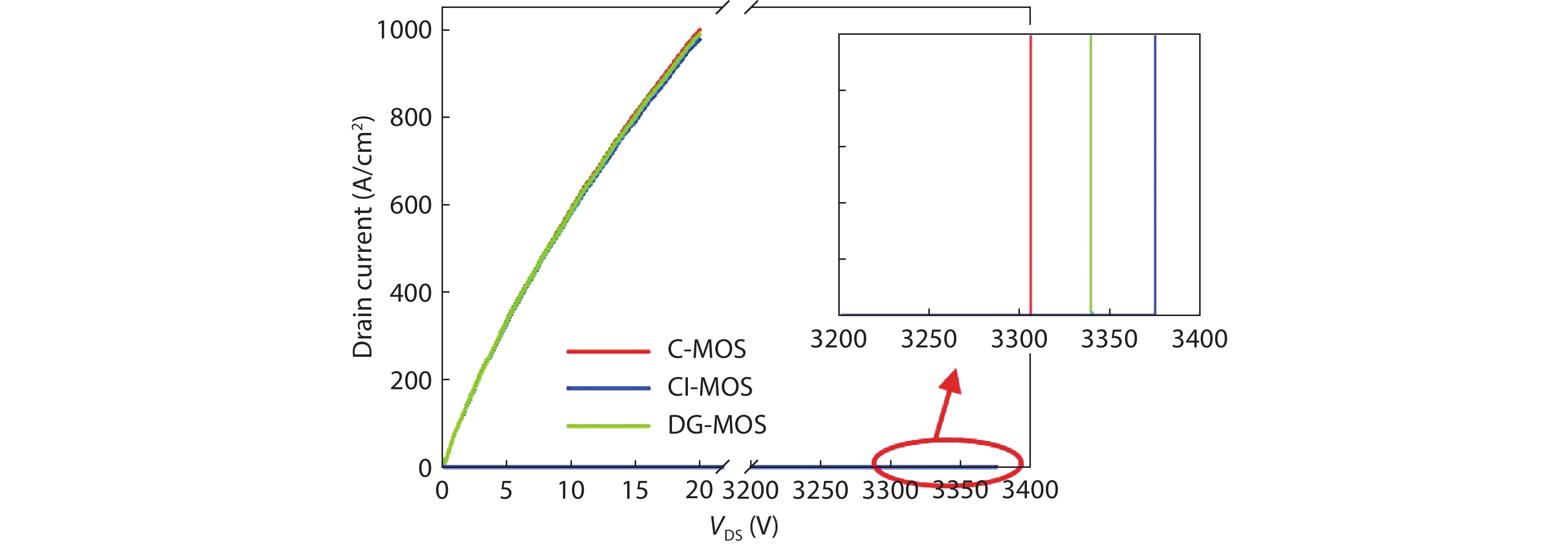
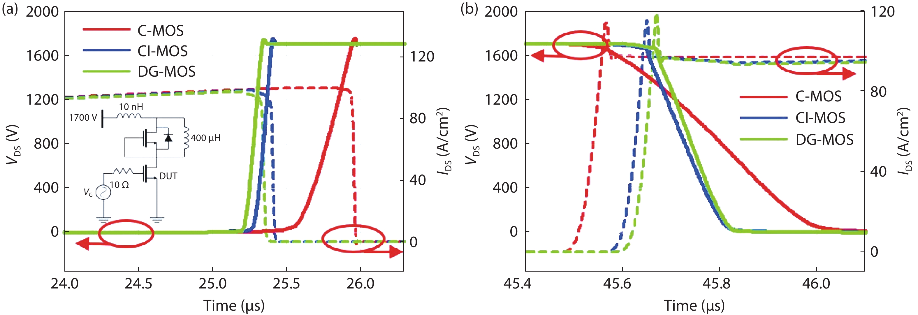
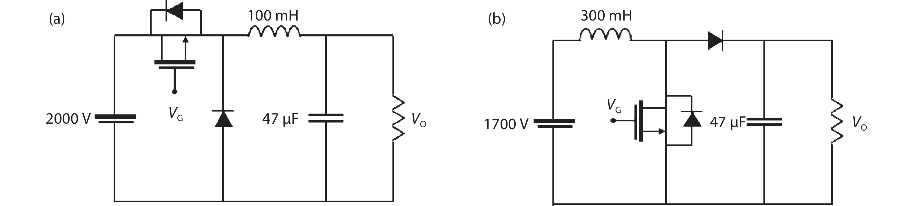
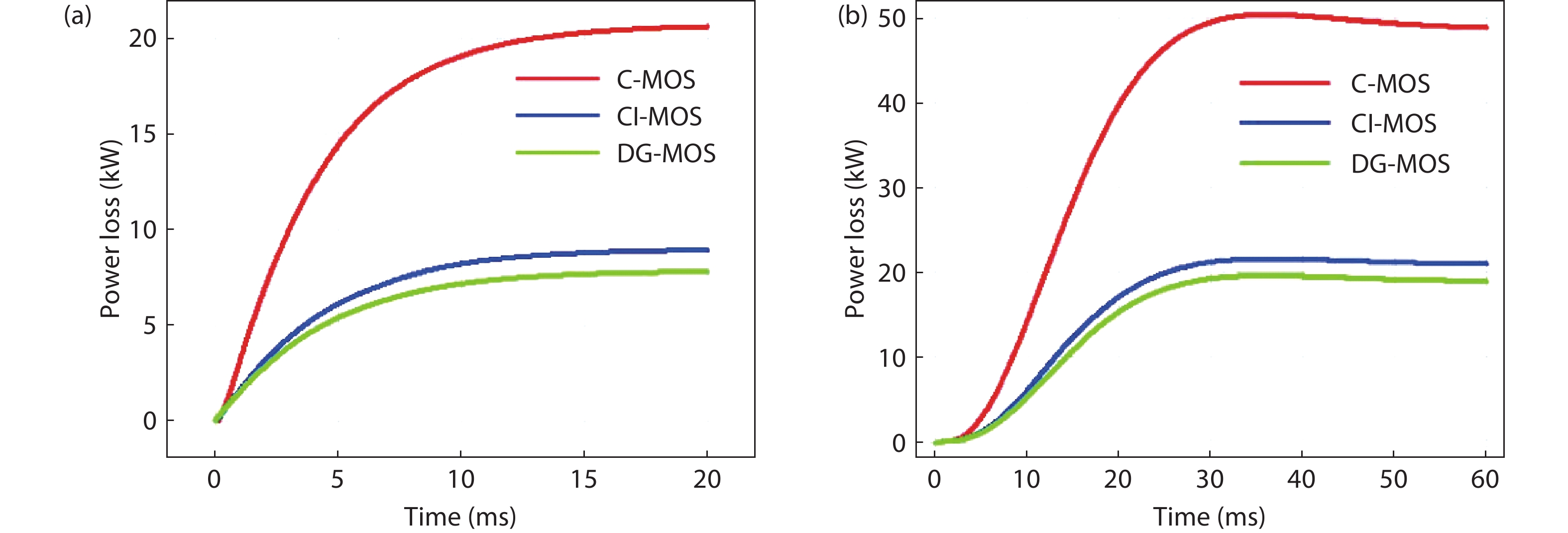
In this paper, a 4H-SiC DMOSFET with a source-contacted dummy gate (DG-MOSFET) is proposed and analyzed through Sentaurus TCAD and PSIM simulations. The source-contacted MOS structure forms fewer depletion regions than the PN junction. Therefore, the overlapping region between the gate and the drain can be significantly reduced while limiting RON degradation. As a result, the DG-MOSFET offers an improved high-frequency figure of merit (HF-FOM) over the conventional DMOSFET (C-MOSFET) and central-implant MOSFET (CI-MOSFET). The HF-FOM (RON×QGD) of the DG-MOSFET was improved by 59.2% and 22.2% compared with those of the C-MOSFET and CI-MOSFET, respectively. In a double-pulse test, the DG-MOSFET could save total power losses of 53.4% and 5.51%, respectively. Moreover, in a power circuit simulation, the switching power loss was reduced by 61.9% and 12.7% in a buck converter and 61% and 9.6% in a boost converter.


J. Semicond.
2021, 42(6): 062802 doi: 10.1088/1674-4926/42/6/062802
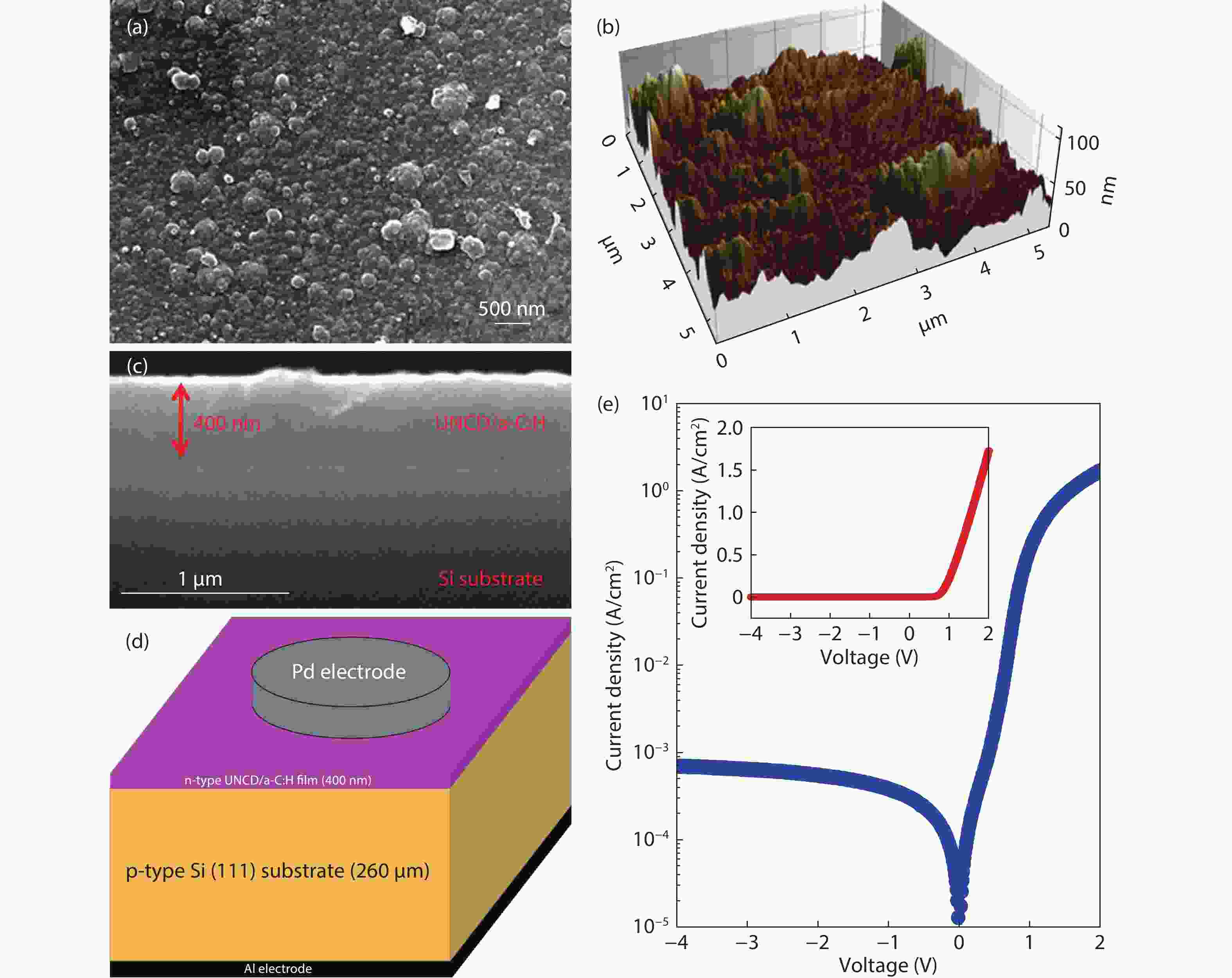
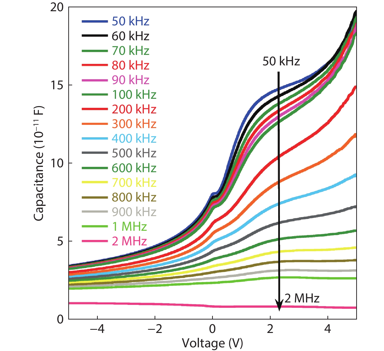
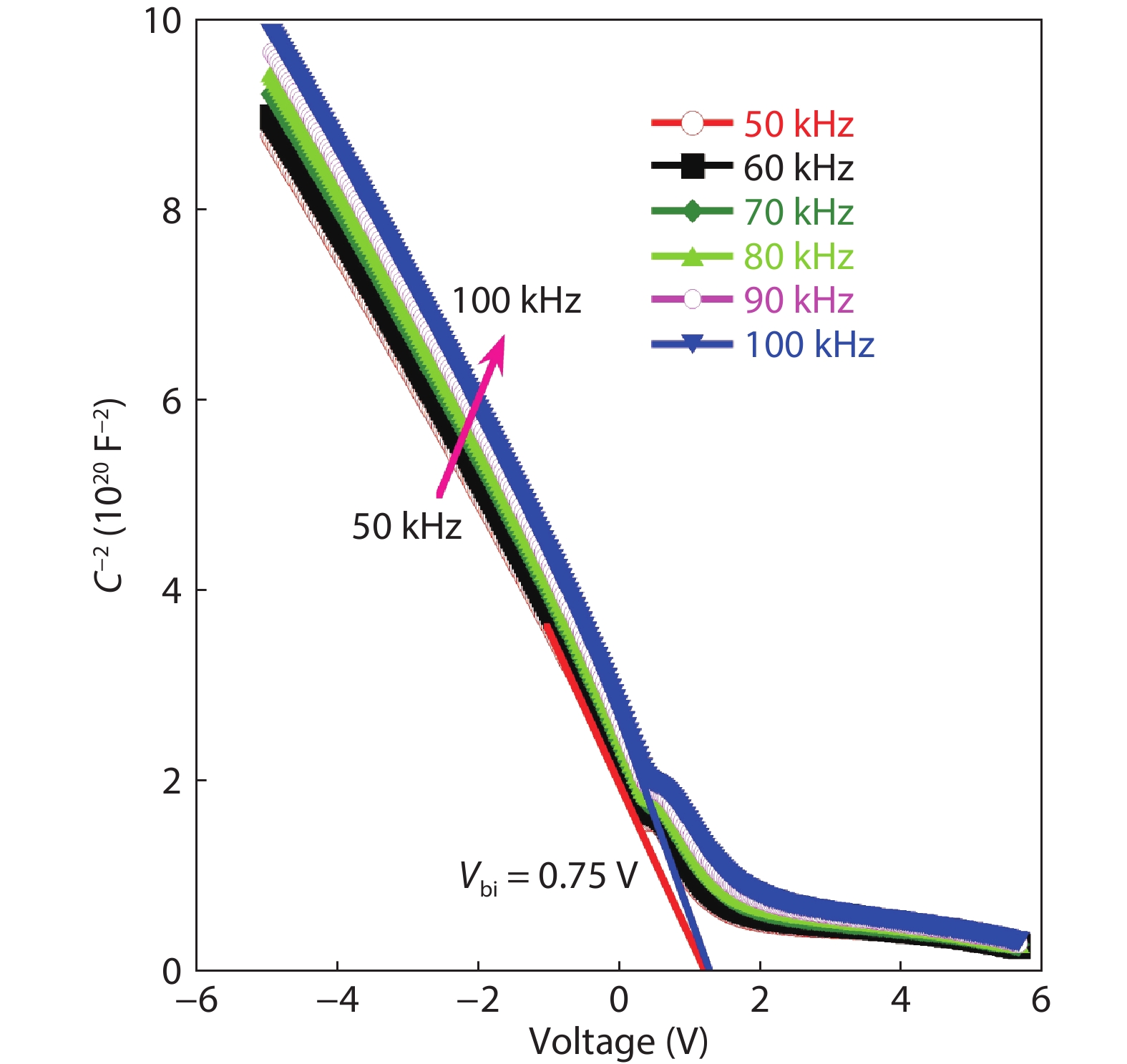
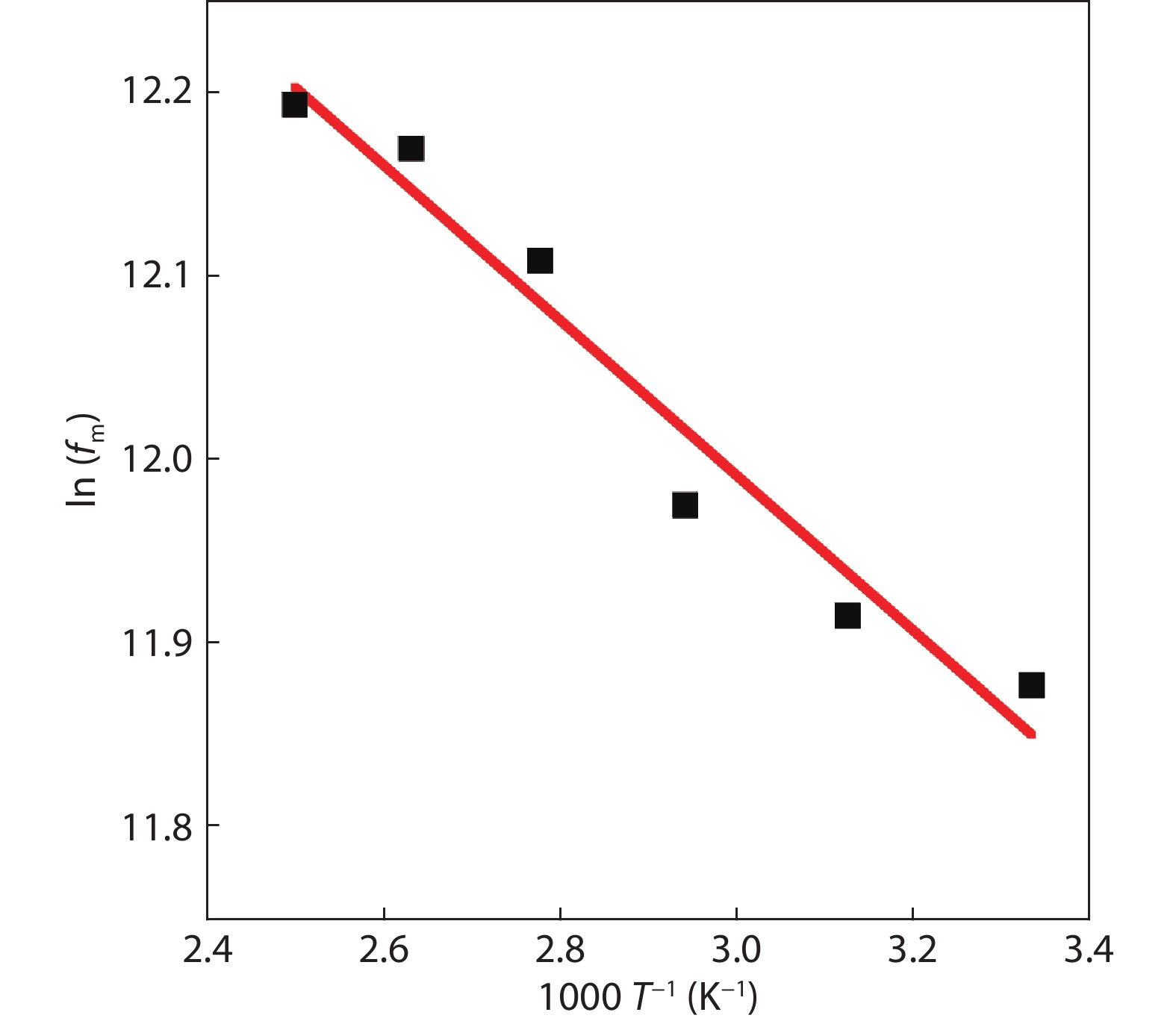
Thin films comprising nitrogen-doped ultrananocrystalline diamond/hydrogenated amorphous-carbon (UNCD/a-C:H) composite films were experimentally investigated. The prepared films were grown on Si substrates by the coaxial arc plasma deposition method. They were characterized by temperature-dependent capacitance-frequency measurements in the temperature and frequency ranges of 300–400 K and 50 kHz–2 MHz, respectively. The energy distribution of trap density of states in the films was extracted using a simple technique utilizing the measured capacitance-frequency characteristics. In the measured temperature range, the energy-distributed traps exhibited Gaussian-distributed states with peak values lie in the range: 2.84 × 10¹⁶–2.73 × 10¹⁷ eV–1 cm–3 and centered at energies of 120–233 meV below the conduction band. These states are generated due to a large amount of sp2-C and π-bond states, localized in GBs of the UNCD/a-C:H film. The attained defect parameters are accommodating to understand basic electrical properties of UNCD/a-C:H composite and can be adopted to suppress defects in the UNCD-based materials.


J. Semicond.
2021, 42(6): 062803 doi: 10.1088/1674-4926/42/6/062803
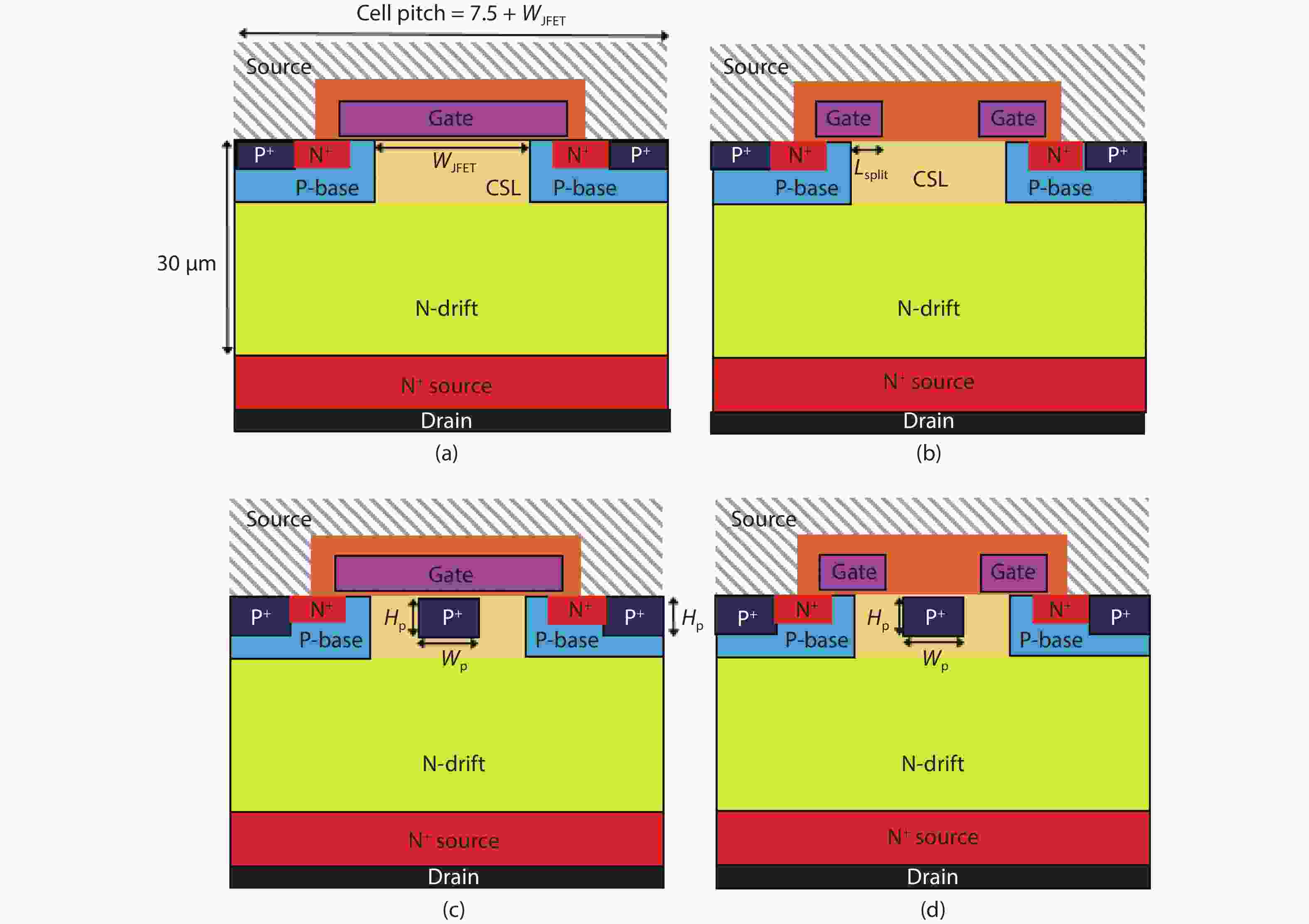
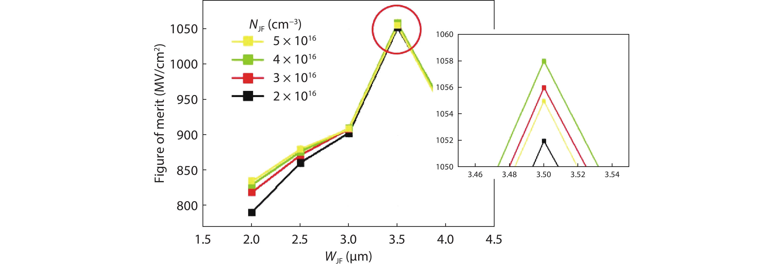
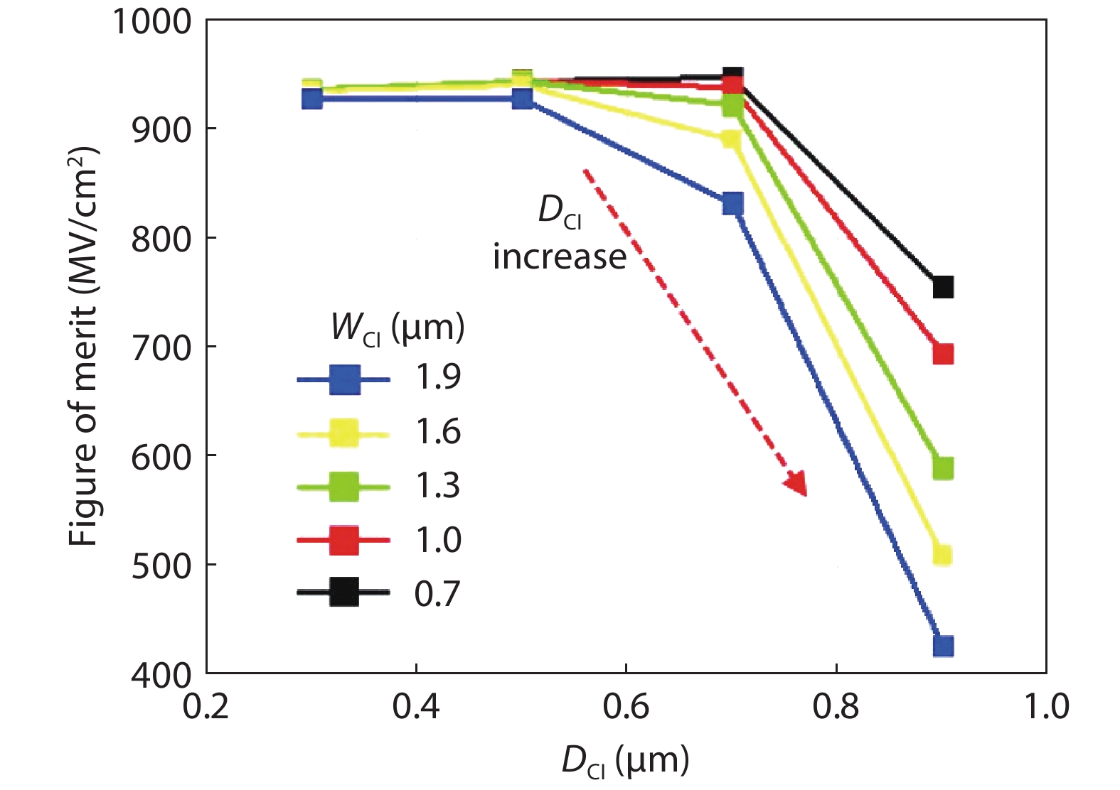
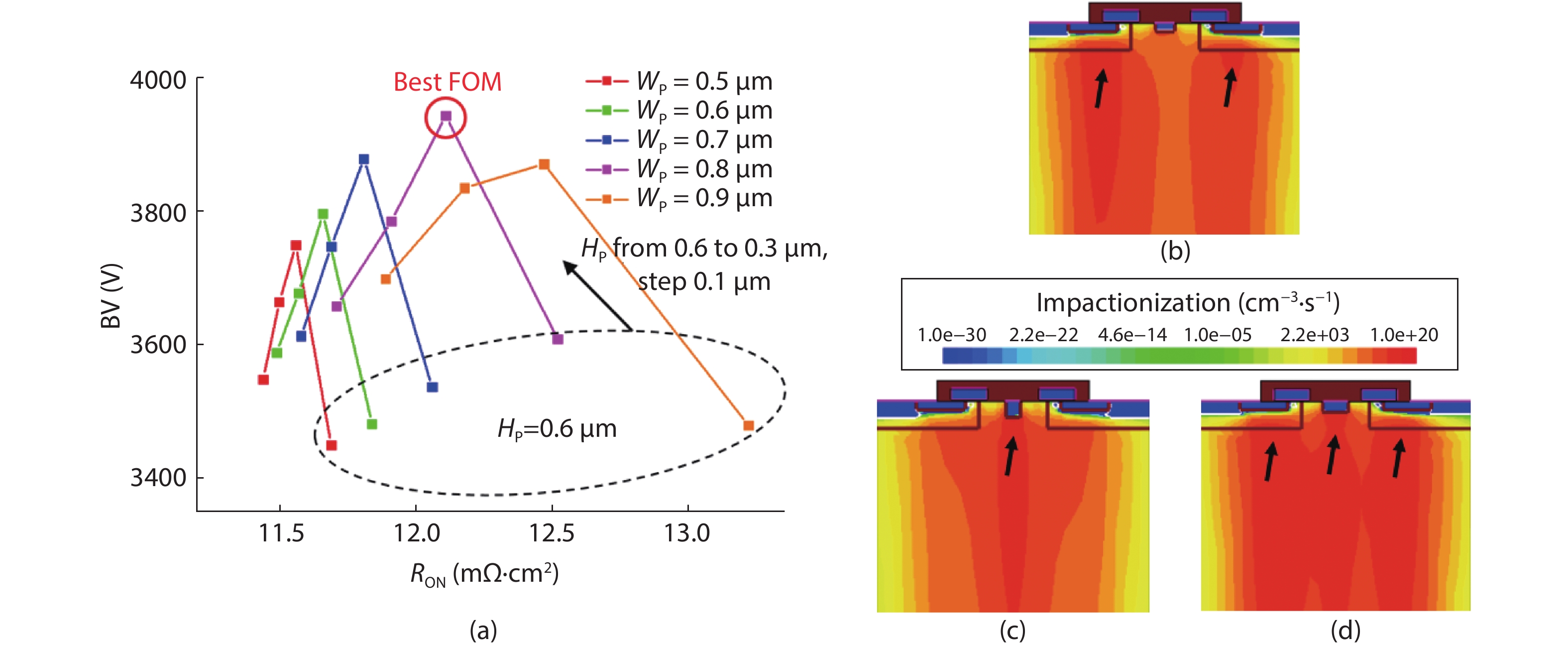
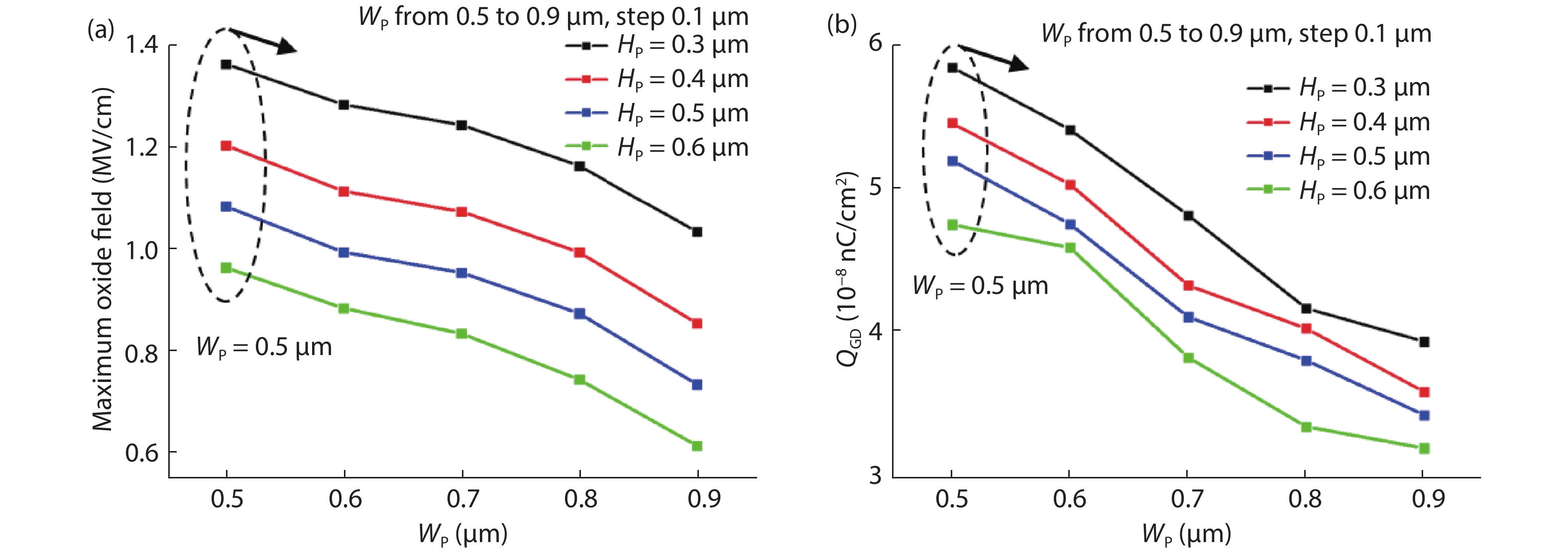
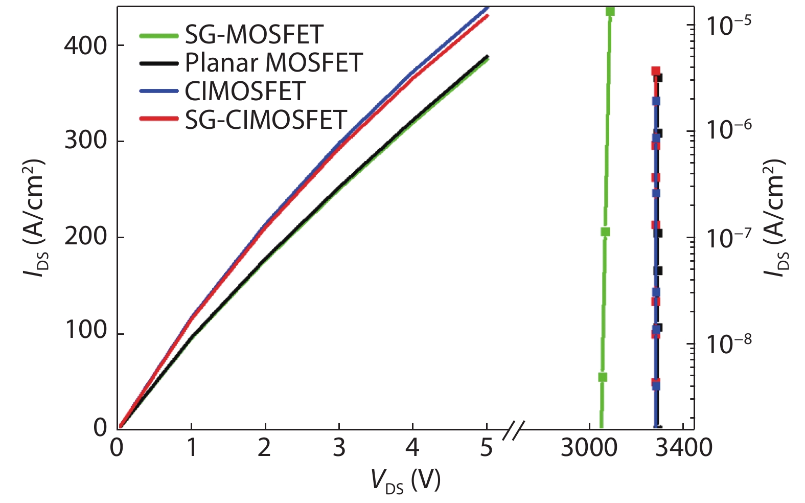
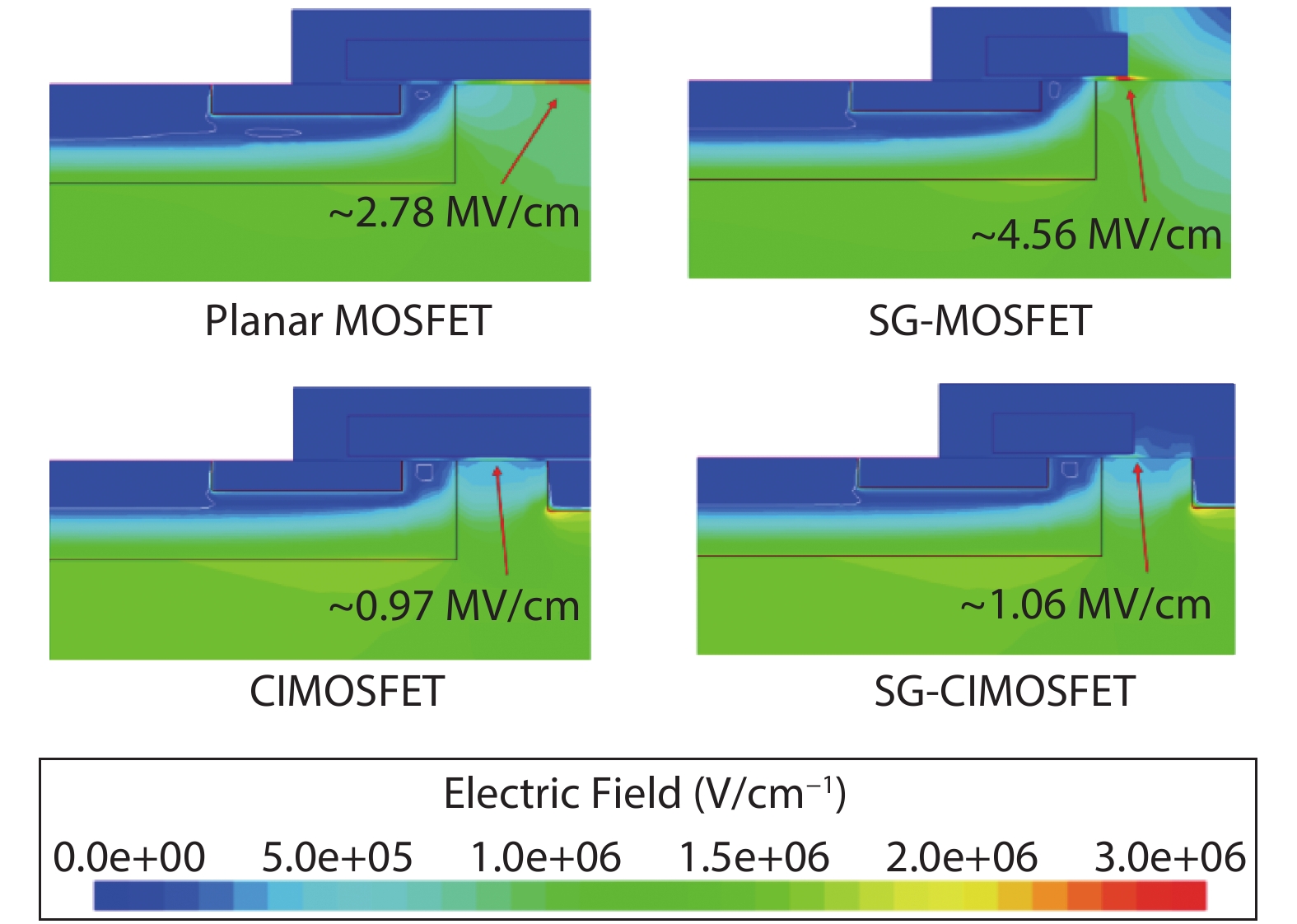
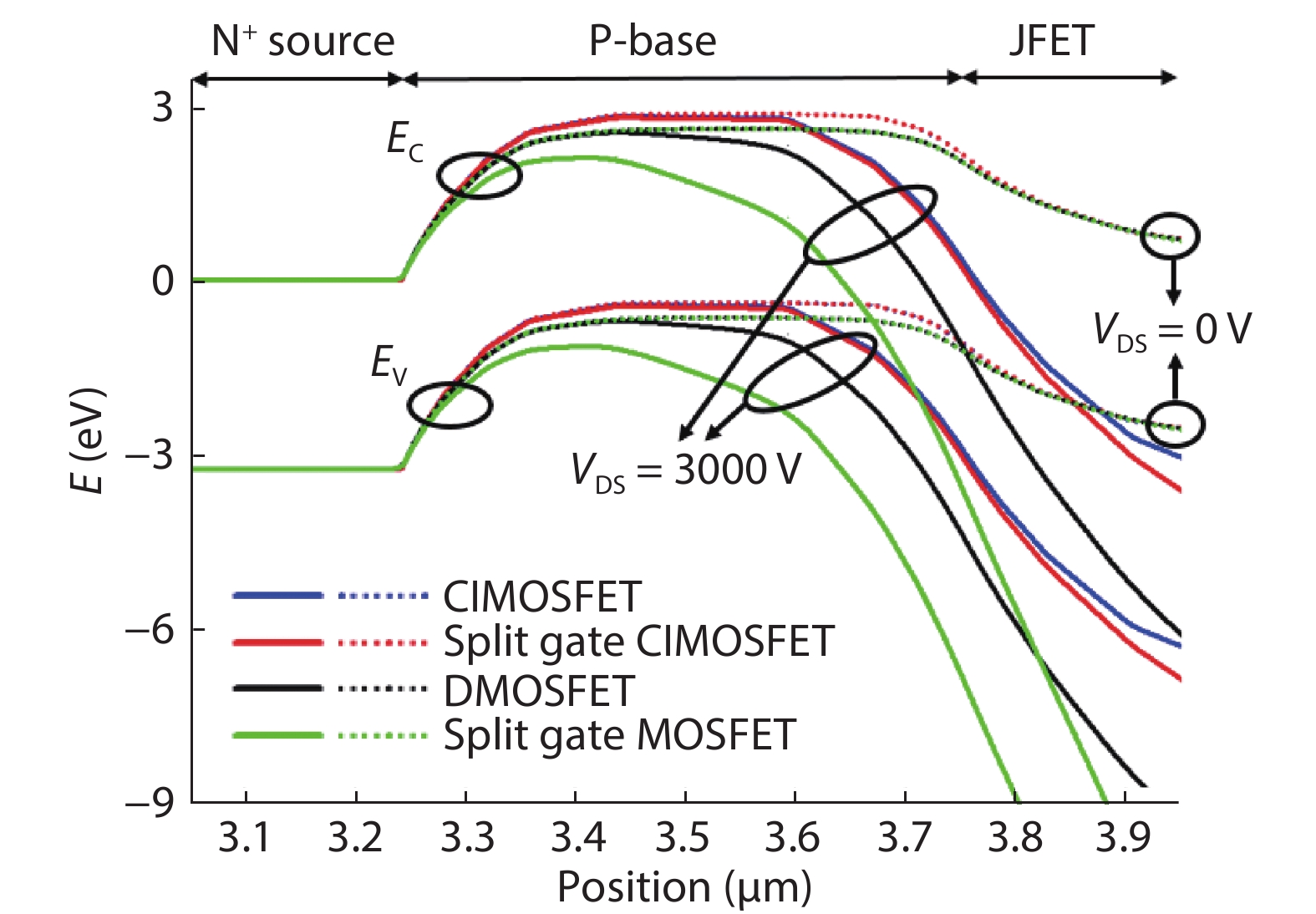
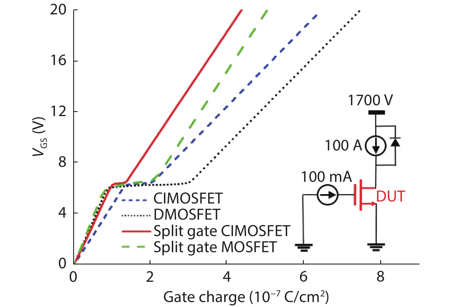
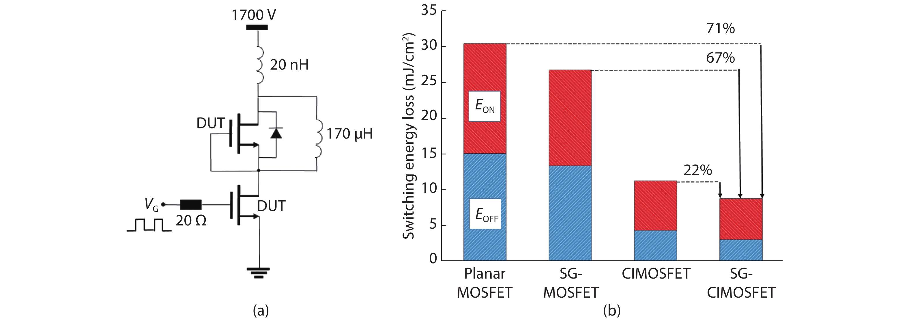
A split gate MOSFET (SG-MOSFET) is widely known for reducing the reverse transfer capacitance (CRSS). In a 3.3 kV class, the SG-MOSFET does not provide reliable operation due to the high gate oxide electric field. In addition to the poor static performance, the SG-MOSFET has issues such as the punch through and drain-induced barrier lowering (DIBL) caused by the high gate oxide electric field. As such, a 3.3 kV 4H-SiC split gate MOSFET with a grounded central implant region (SG-CIMOSFET) is proposed to resolve these issues and for achieving a superior trade-off between the static and switching performance. The SG-CIMOSFET has a significantly low on-resistance (RON) and maximum gate oxide field (EOX) due to the central implant region. A grounded central implant region significantly reduces the CRSS and gate drain charge (QGD) by partially screening the gate-to-drain capacitive coupling. Compared to a planar MOSFET, the SG MOSFET, central implant MOSFET (CIMOSFET), the SG-CIMOSFET improve the RON×QGD by 83.7%, 72.4% and 44.5%, respectively. The results show that the device features not only the smallest switching energy loss but also the fastest switching time.


J. Semicond.
2021, 42(6): 064101 doi: 10.1088/1674-4926/42/6/064101
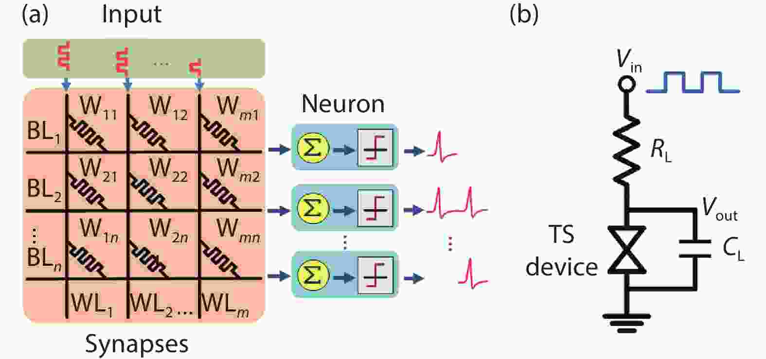
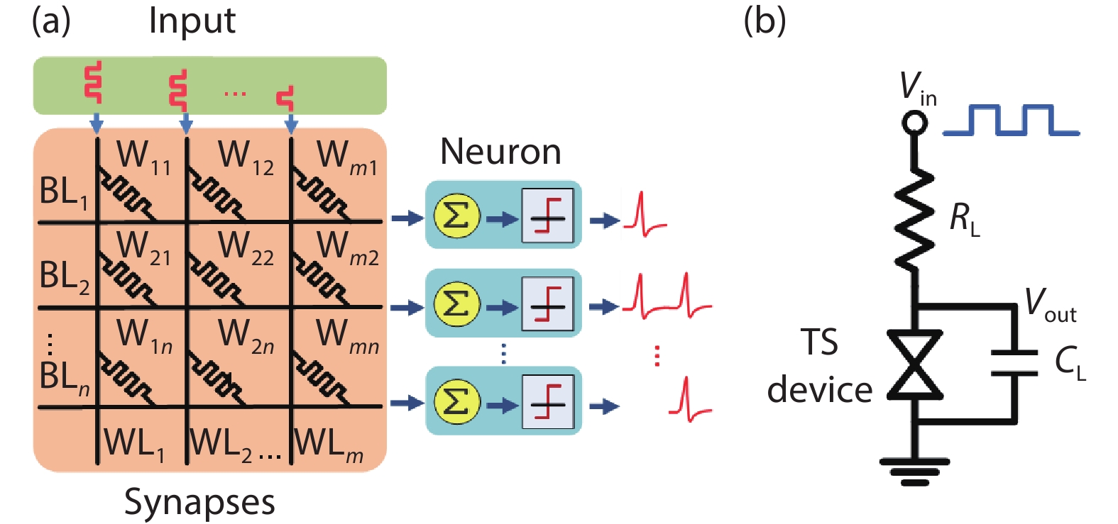
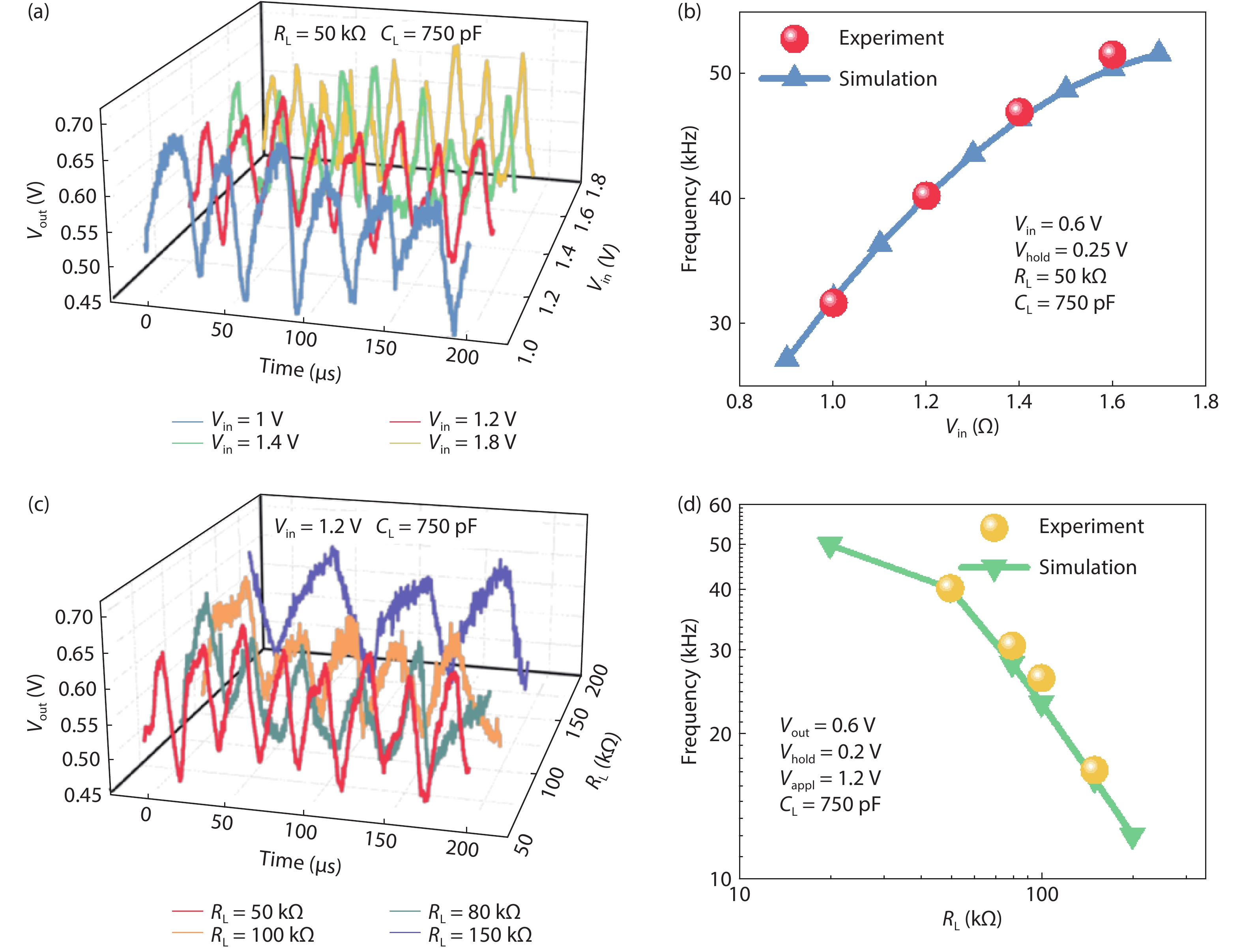
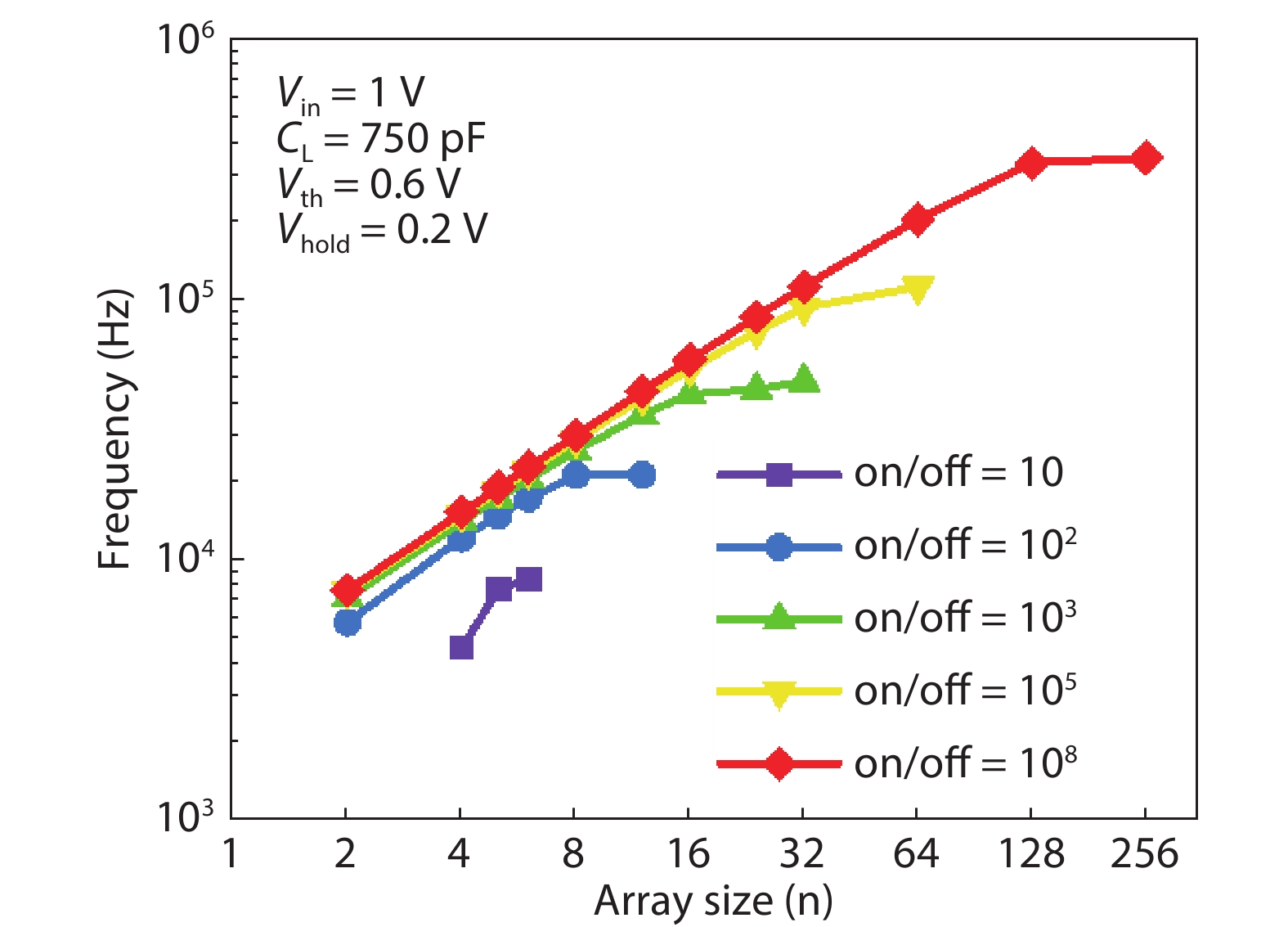
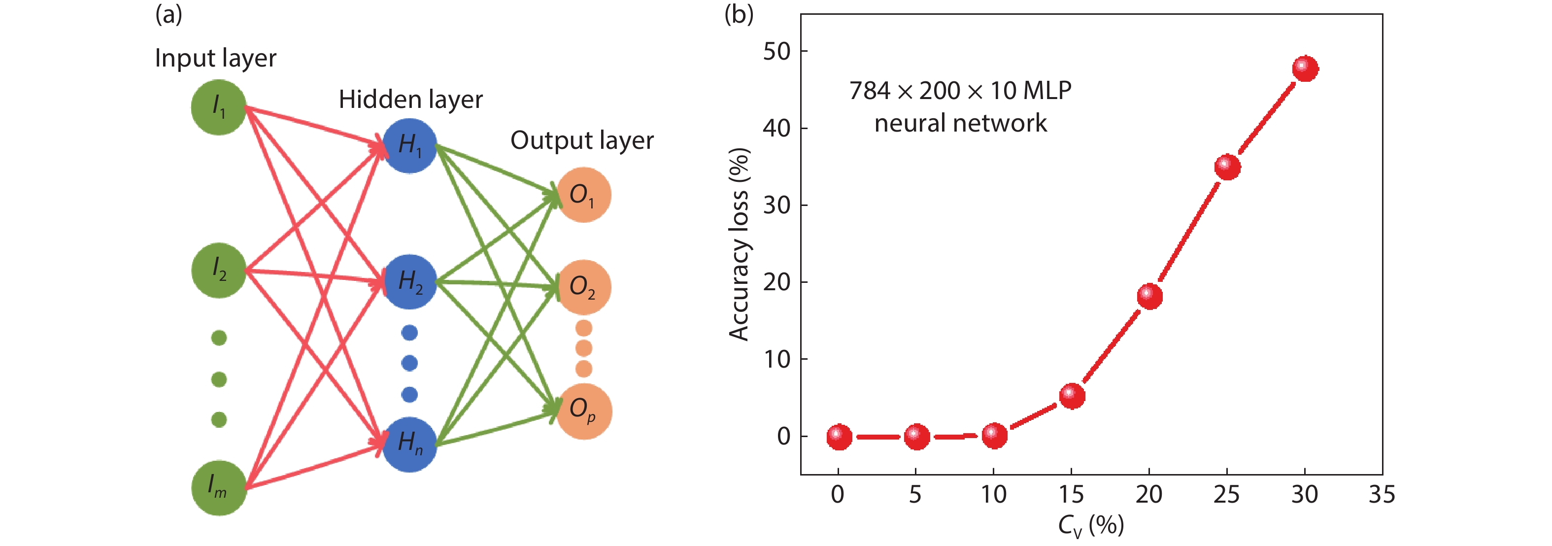
Low-power and low-variability artificial neuronal devices are highly desired for high-performance neuromorphic computing. In this paper, an oscillation neuron based on a low-variability Ag nanodots (NDs) threshold switching (TS) device with low operation voltage, large on/off ratio and high uniformity is presented. Measurement results indicate that this neuron demonstrates self-oscillation behavior under applied voltages as low as 1 V. The oscillation frequency increases with the applied voltage pulse amplitude and decreases with the load resistance. It can then be used to evaluate the resistive random-access memory (RRAM) synaptic weights accurately when the oscillation neuron is connected to the output of the RRAM crossbar array for neuromorphic computing. Meanwhile, simulation results show that a large RRAM crossbar array (> 128 × 128) can be supported by our oscillation neuron owing to the high on/off ratio (> 108) of Ag NDs TS device. Moreover, the high uniformity of the Ag NDs TS device helps improve the distribution of the output frequency and suppress the degradation of neural network recognition accuracy (< 1%). Therefore, the developed oscillation neuron based on the Ag NDs TS device shows great potential for future neuromorphic computing applications.