Issue Browser
Volume 42, Issue 7,
Jul 2021


J. Semicond.
2021, 42(7): 071901 doi: 10.1088/1674-4926/42/7/071901
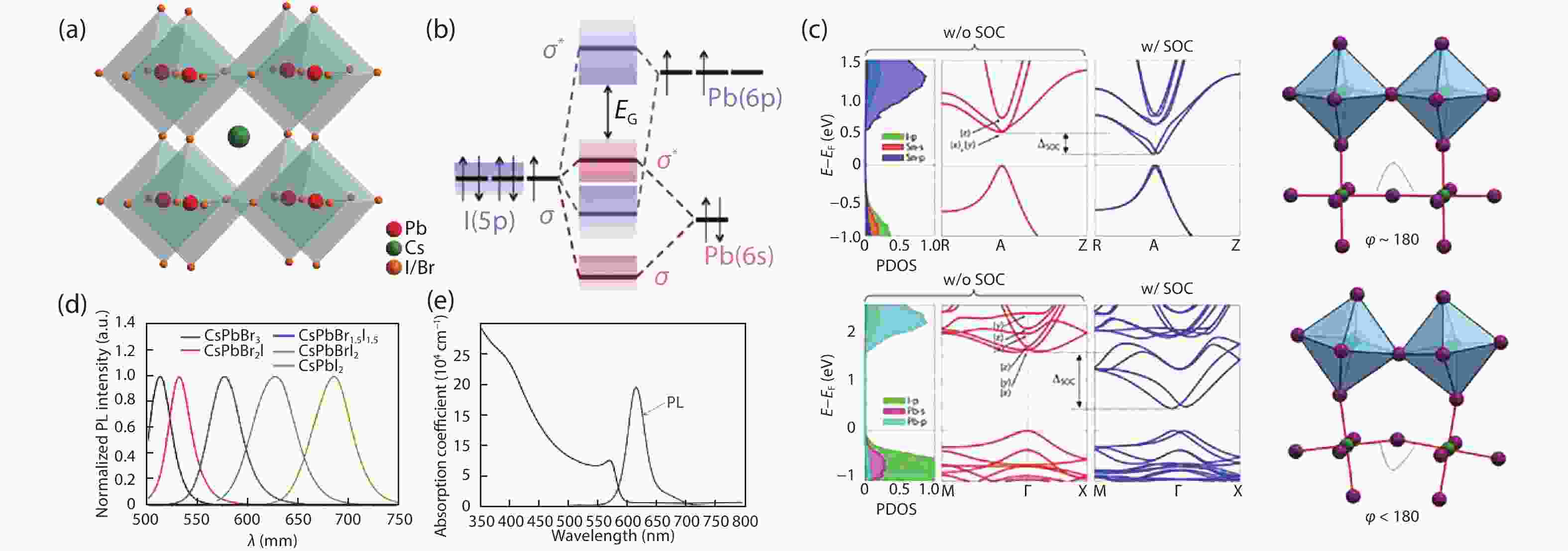
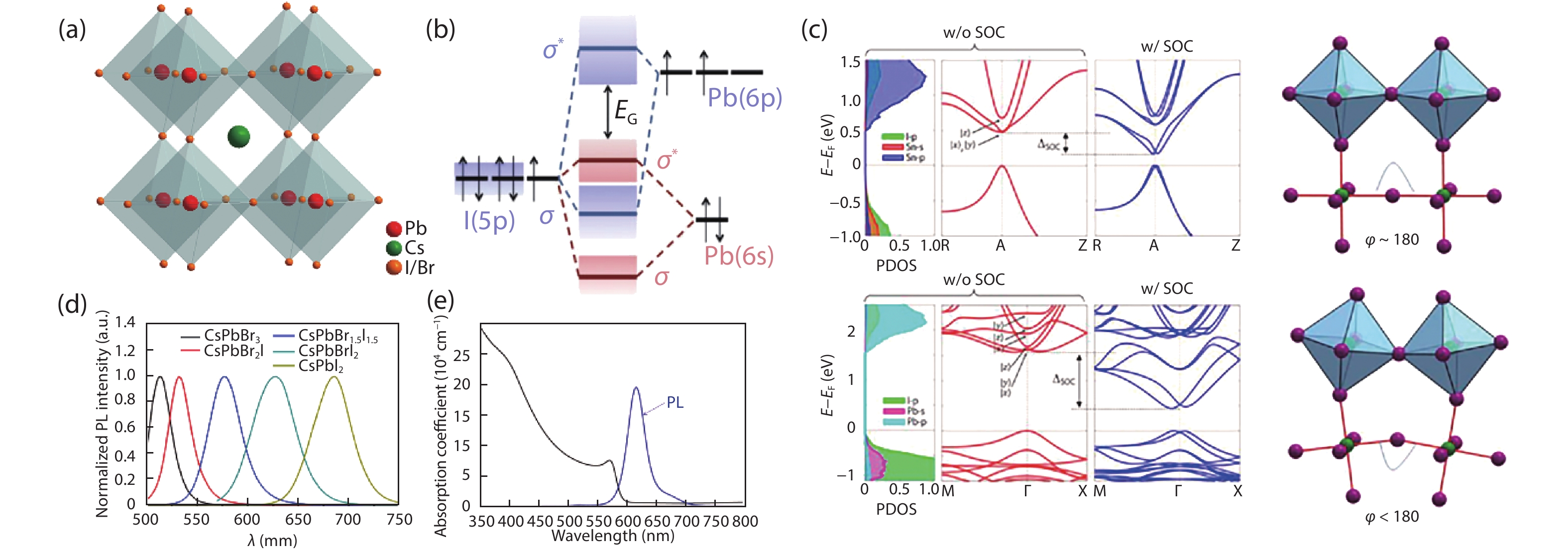
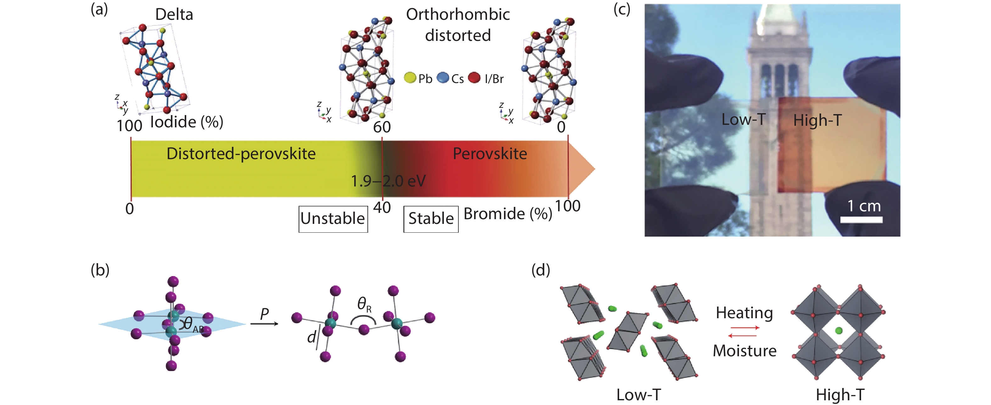
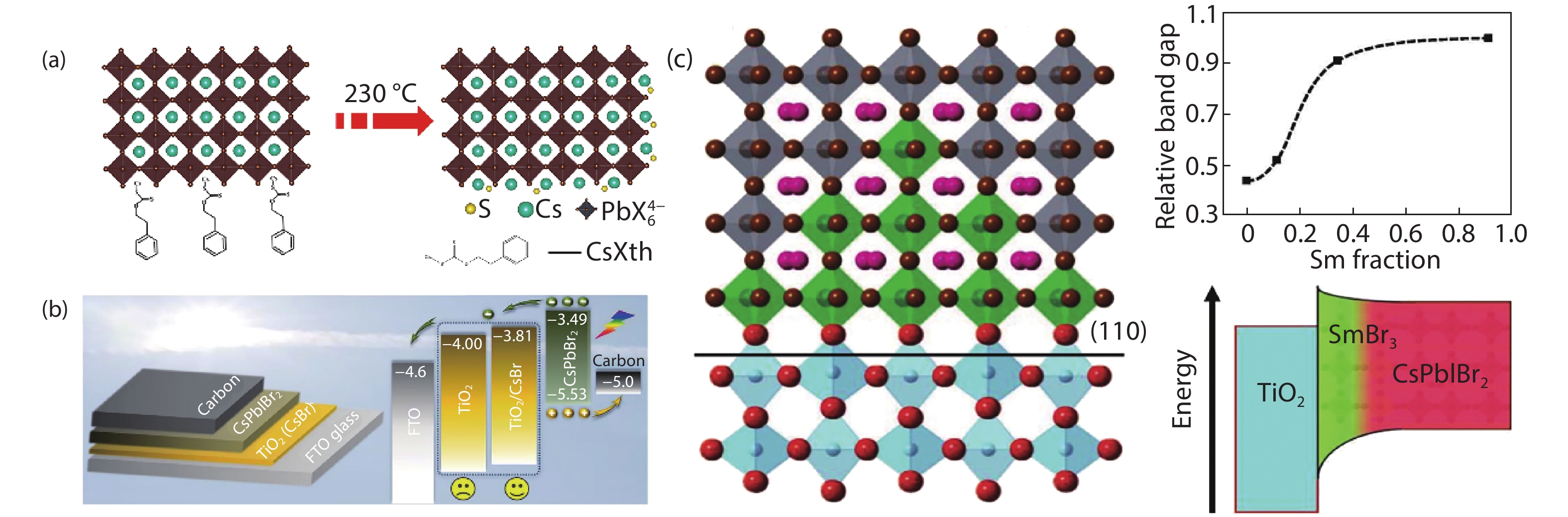
The rapid rise in the power conversion efficiency (PCE) of CsPbBr2I-based perovskite solar cells (PSCs), from 4.7% in 2016 to 11.08% in 2020, render it a promising material for use in photovoltaic devices. However, the phase stability and current hysteresis caused by photo-induced phase segregation in CsPbBr2I represent major obstacles to further improvements in the PCE for such devices. In this review, we describe the basic structure and optical properties of CsPbBr2I, and systematically elaborate on the mechanism of the phase transition. We then discuss the strategies in progress to suppress phase transition in CsPbBr2I, and their potential application in the photovoltaic field. Finally, challenges and application prospects for CsPbBr2I PSCs are summarized in the final section of this article.


J. Semicond.
2021, 42(7): 072201 doi: 10.1088/1674-4926/42/7/072201
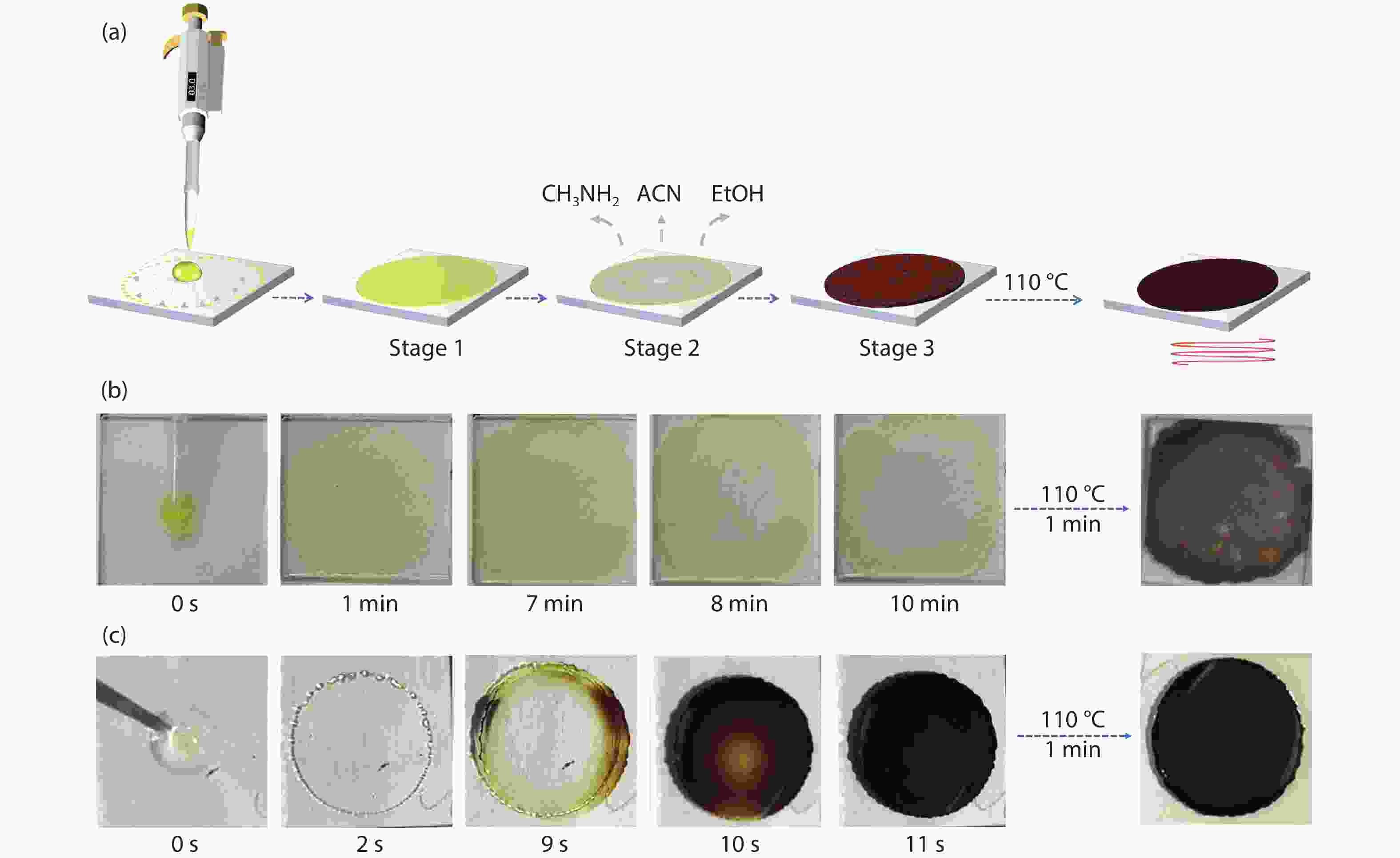
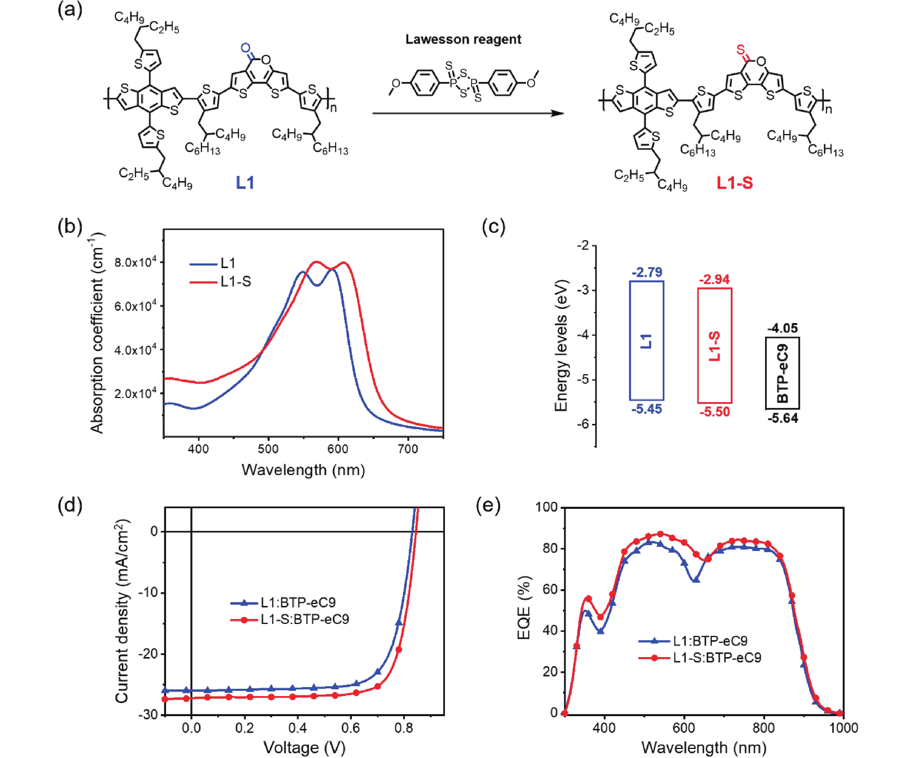
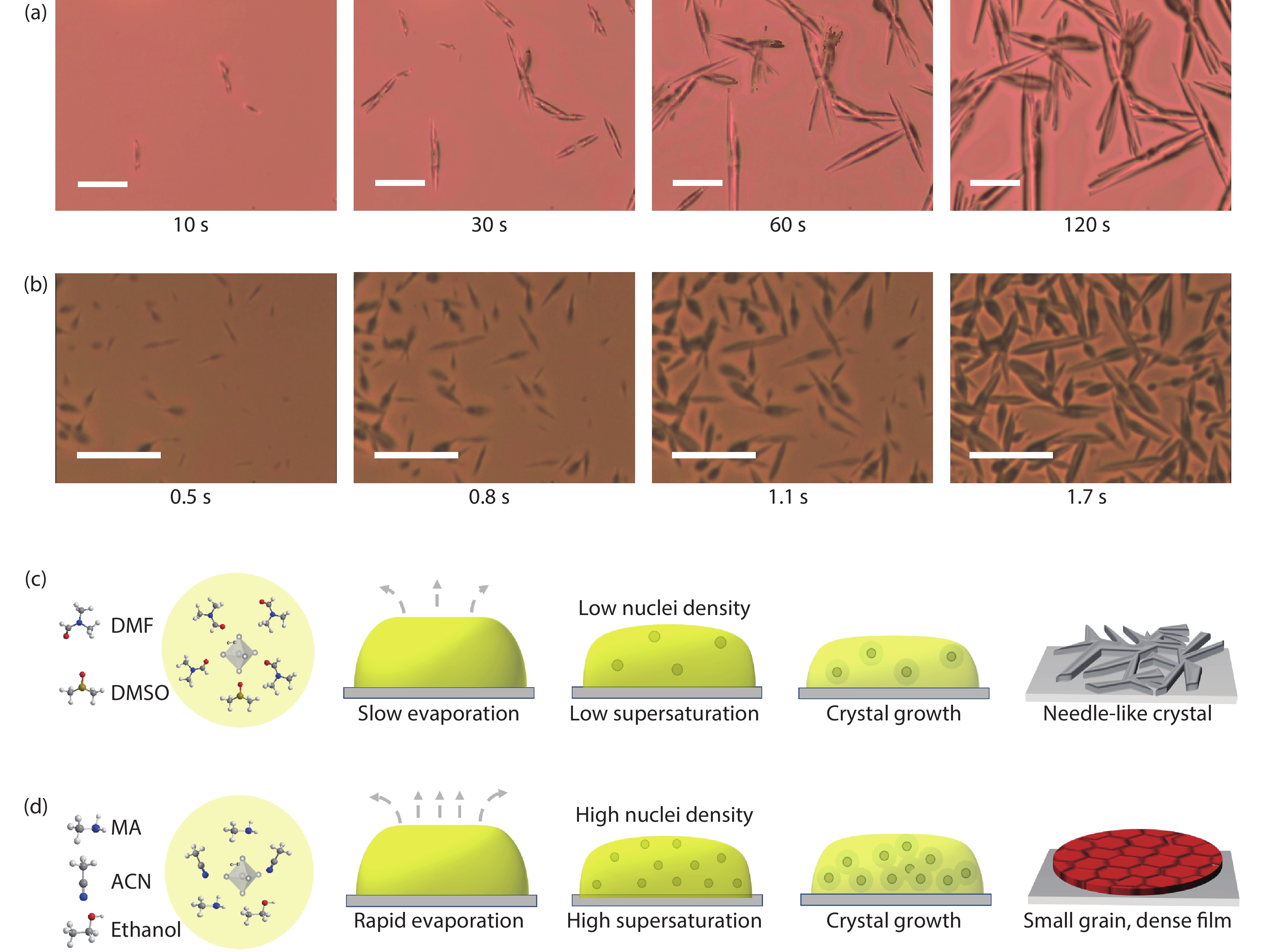
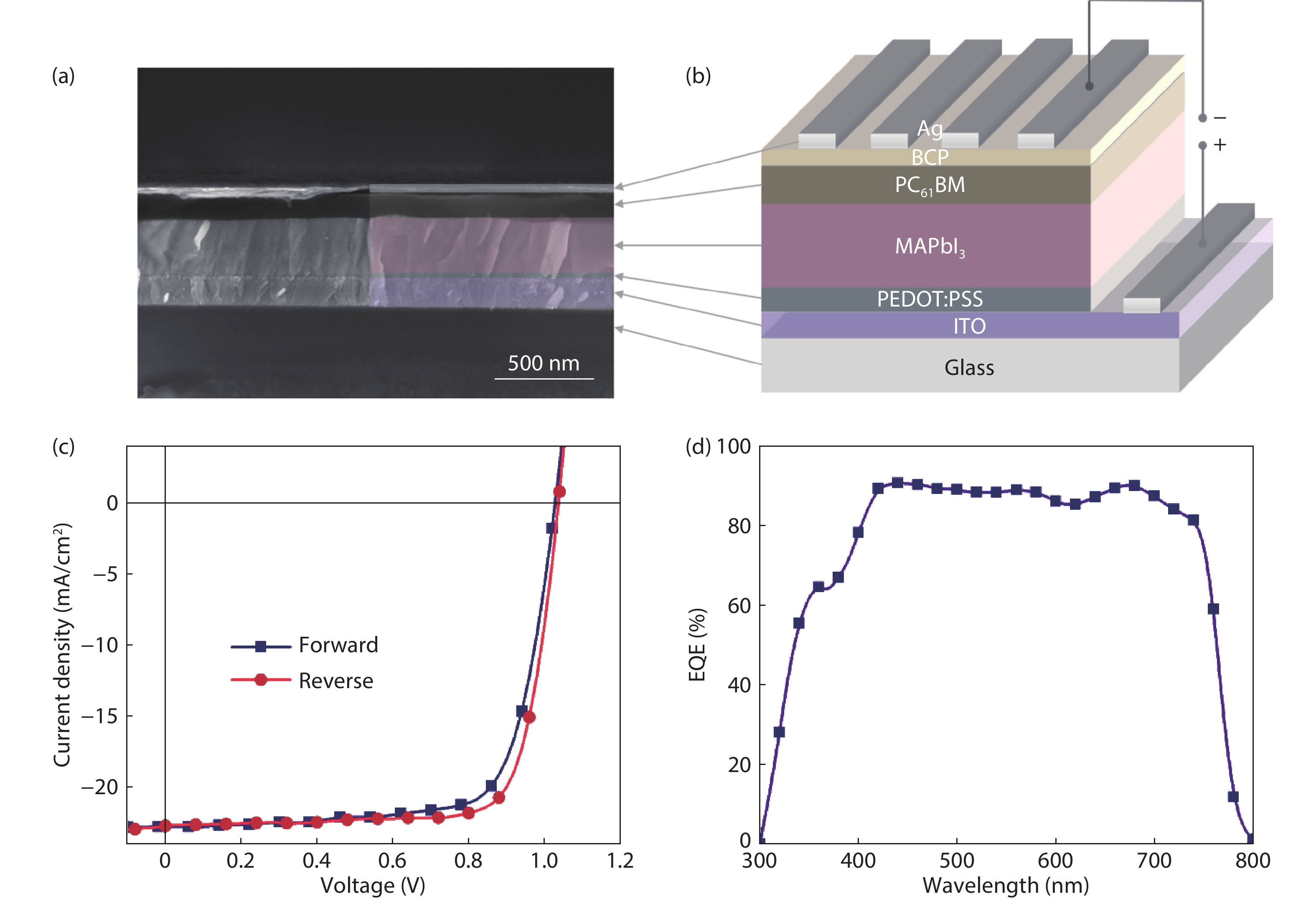
Here we demonstrate a room-temperature drop-coating method for MAPbI3 films. By using low-boiling-point solvent, high-quality MAPbI3 films were made by simply casting a drop of solution onto the substrate at room temperature. This approach took advantage of the synergistic effect of good wettability and volatility of the solvent, enabling high nuclei density and compact film at room temperature. The crystal growth in different solvents was in-situ observed by using optical microscope, which helped us to understand the mechanism for the formation of different film morphology. Perovskite solar cells gave a PCE of 18.21%.


J. Semicond.
2021, 42(7): 072202 doi: 10.1088/1674-4926/42/7/072202
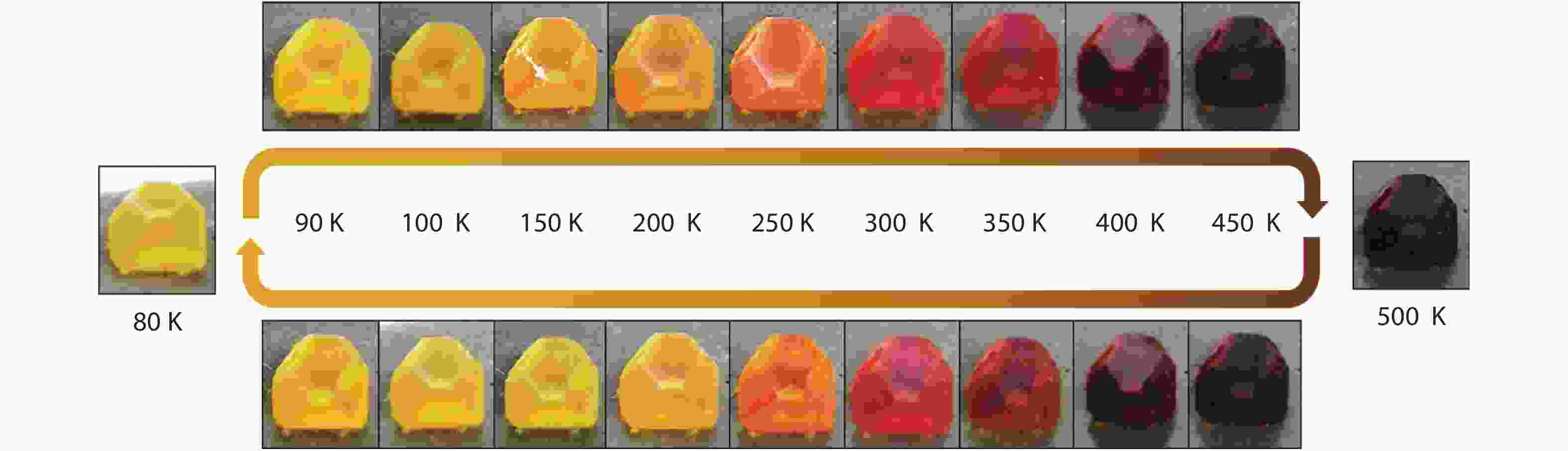
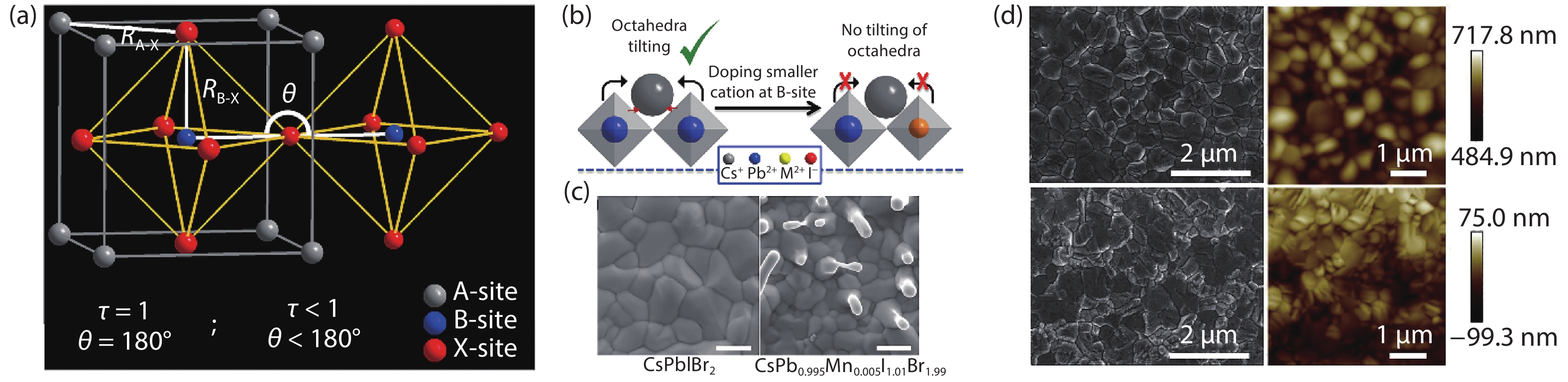
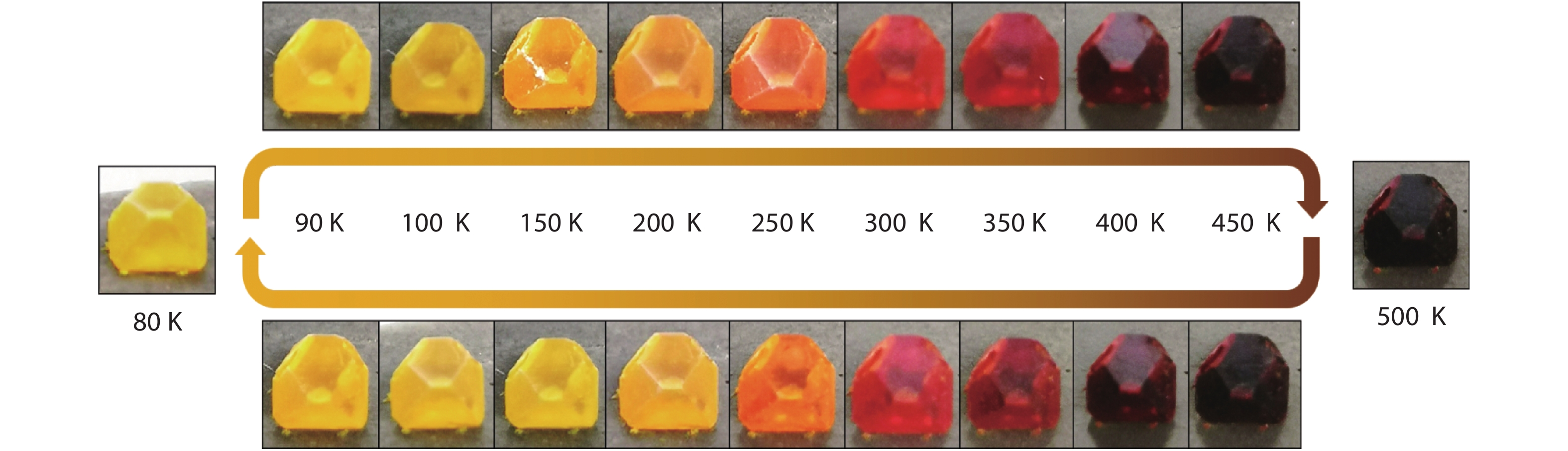
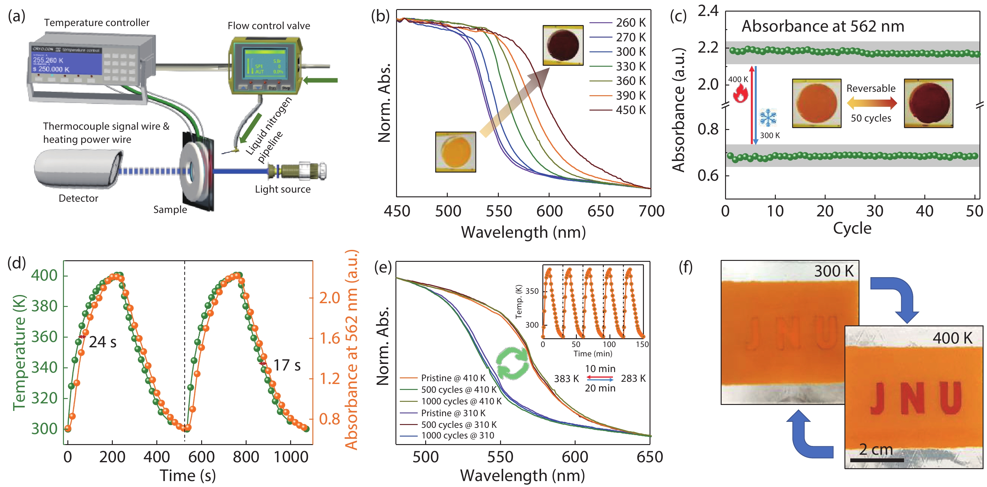
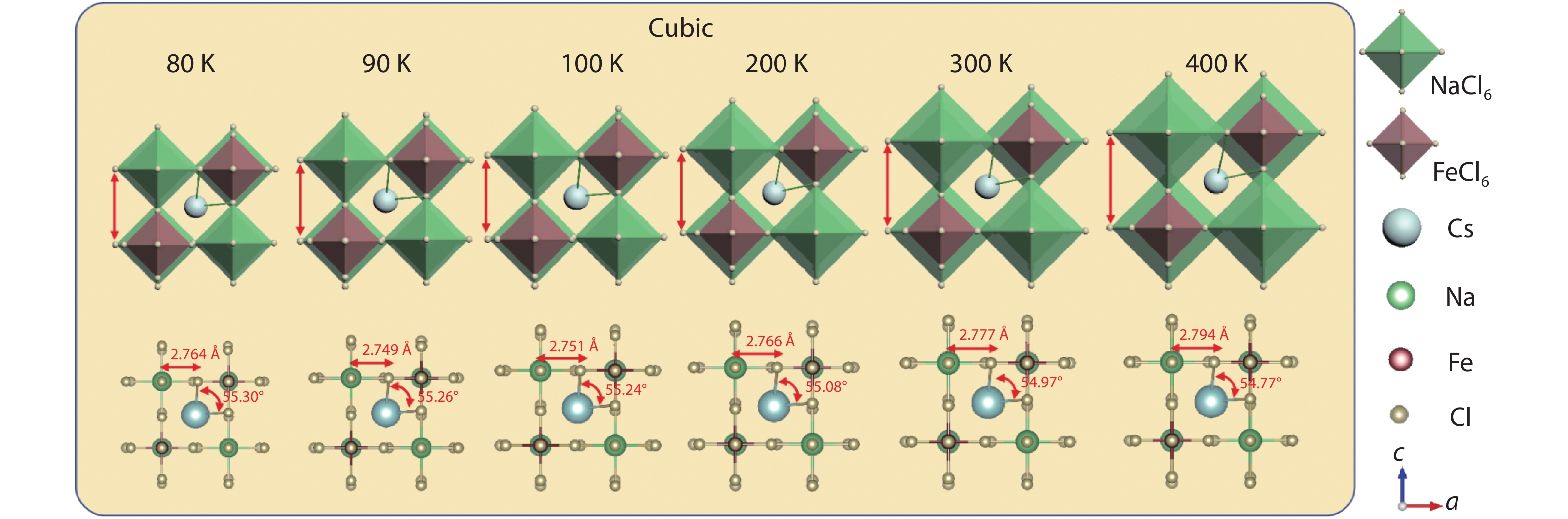
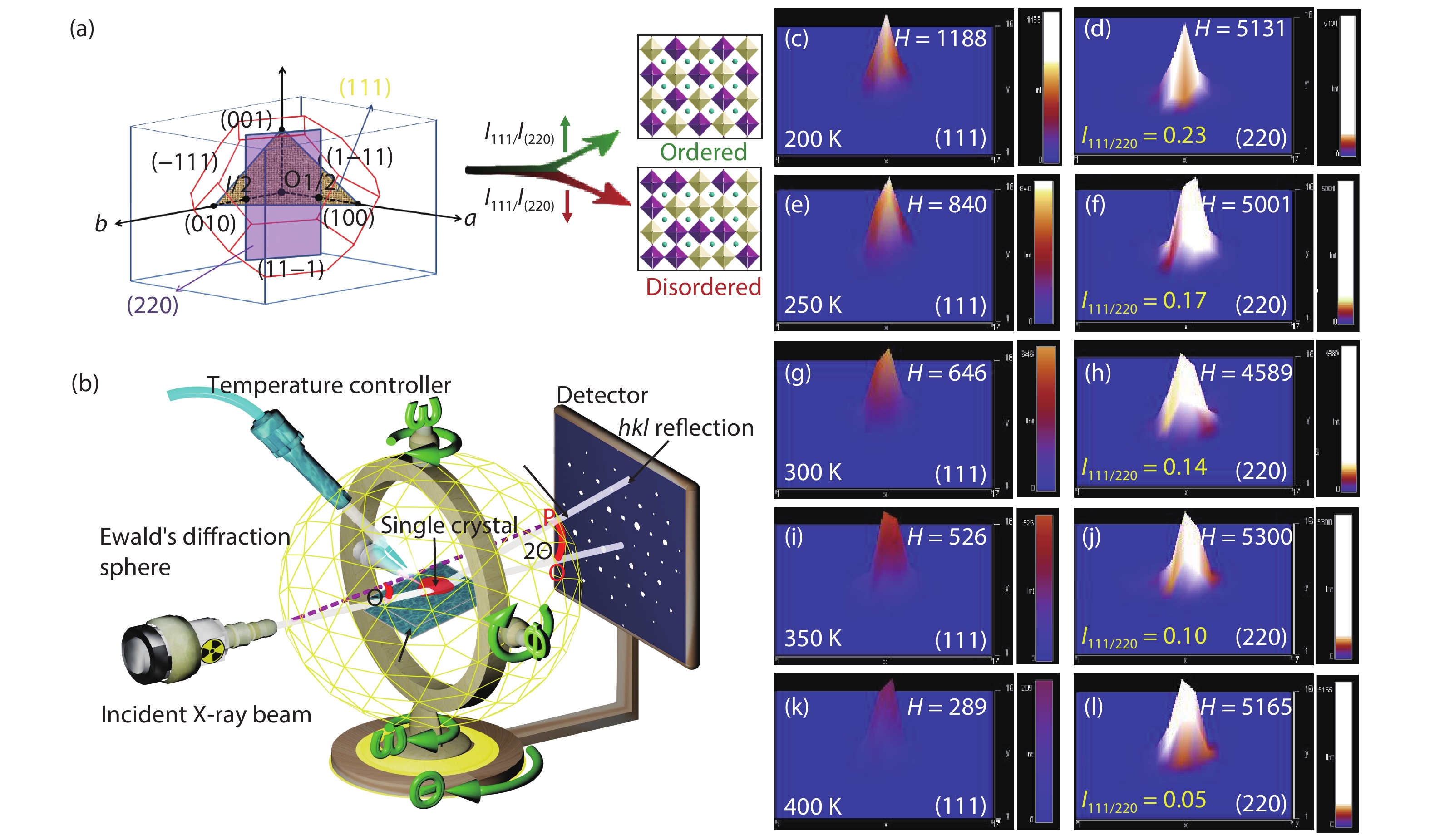
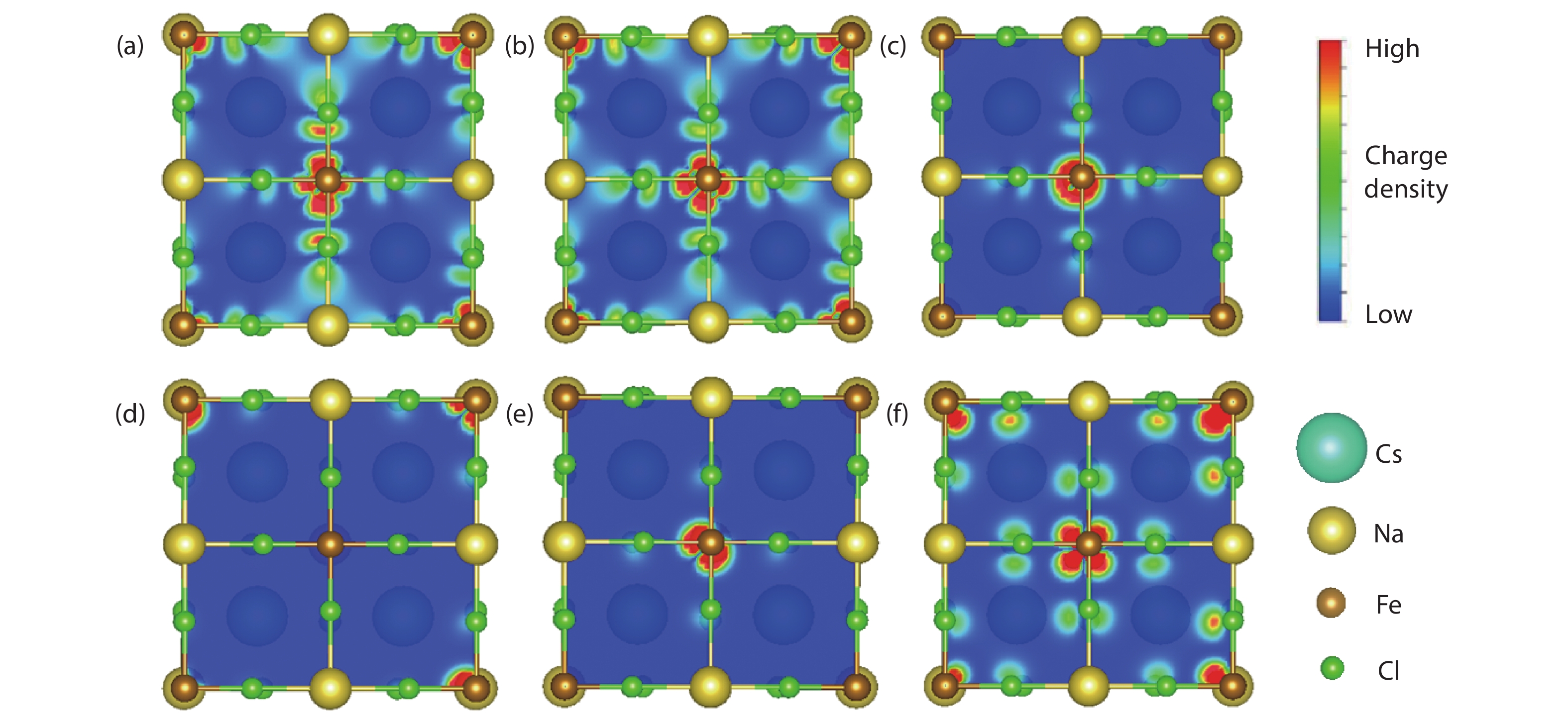
Multifunctional lead-free double perovskites demonstrate remarkable potential towards applications in various fields. Herein, an environmentally-friendly, low-cost, high-throughput Cs2NaFeCl6 single crystal with exceedingly high thermal stability is designed and grown. It obtains a cubic lattice system in the temperature range of 80–500 K, accompanied by a completely reversible chromatic variation ranging from yellow to black. Importantly, the intriguing thermochromism is proved to own extremely high reproducibility (over 1000 cycles) without a hysteretic effect, originating from its structural flexibility that including (i) the noteworthy distortion/deformation of [NaCl6]5− and [FeCl6]3− octahedra; (ii) order–disorder arrangement transition of [NaCl6]5− and [FeCl6]3− octahedra as the function of temperature. This study paves the way towards a new class of smart windows and camouflage coatings with an unprecedented colour range based on a Cs2NaFeCl6 perovskite.
J. Semicond.
2021, 42(7): 072401 doi: 10.1088/1674-4926/42/7/072401

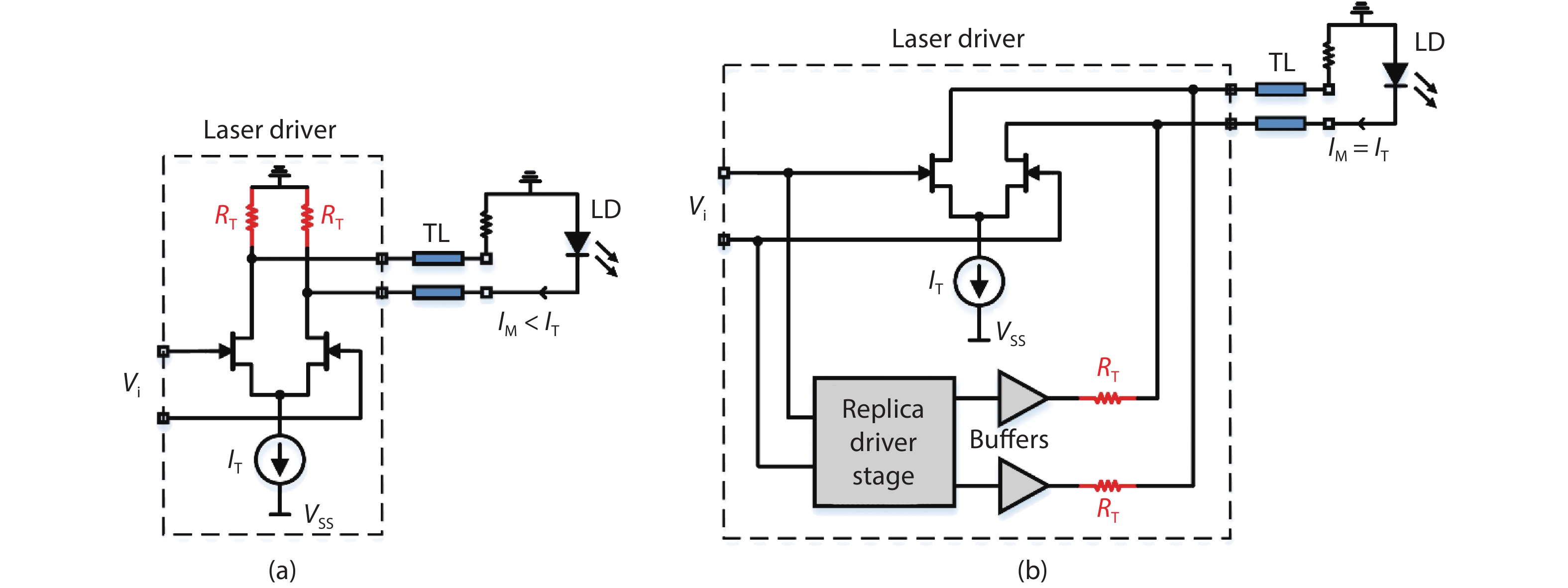
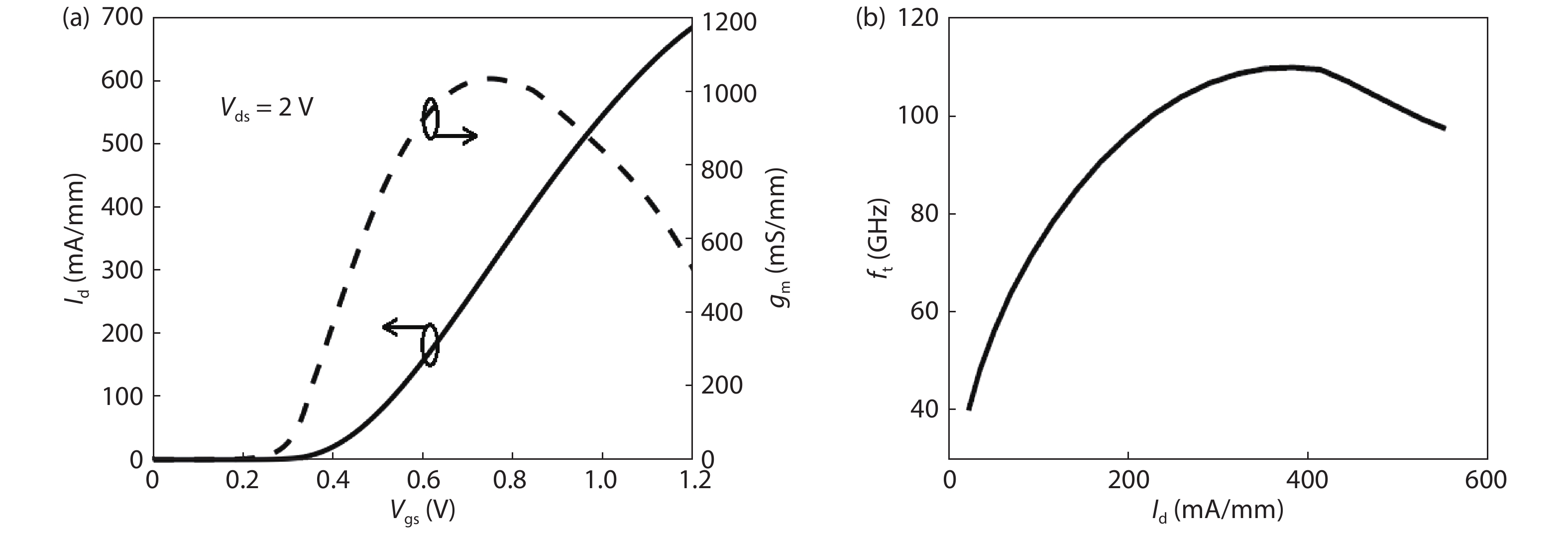
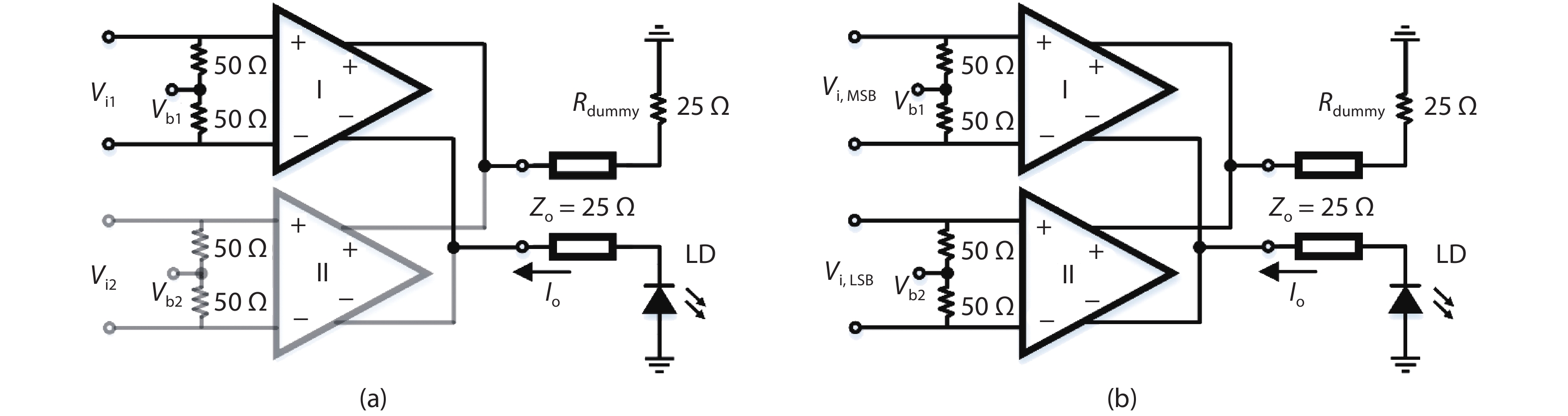
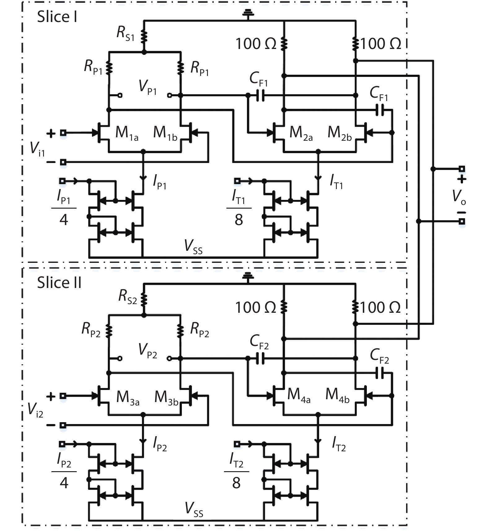
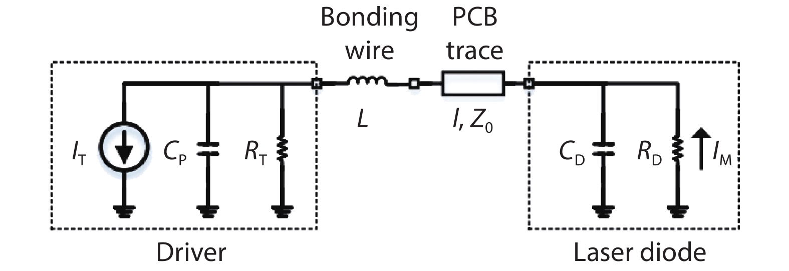
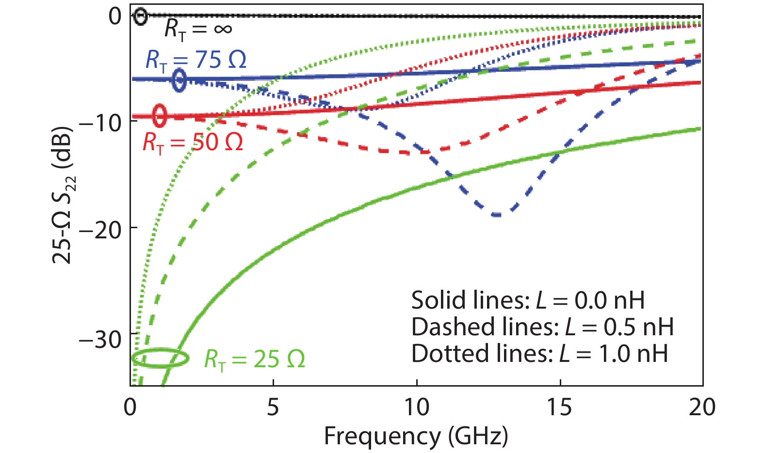
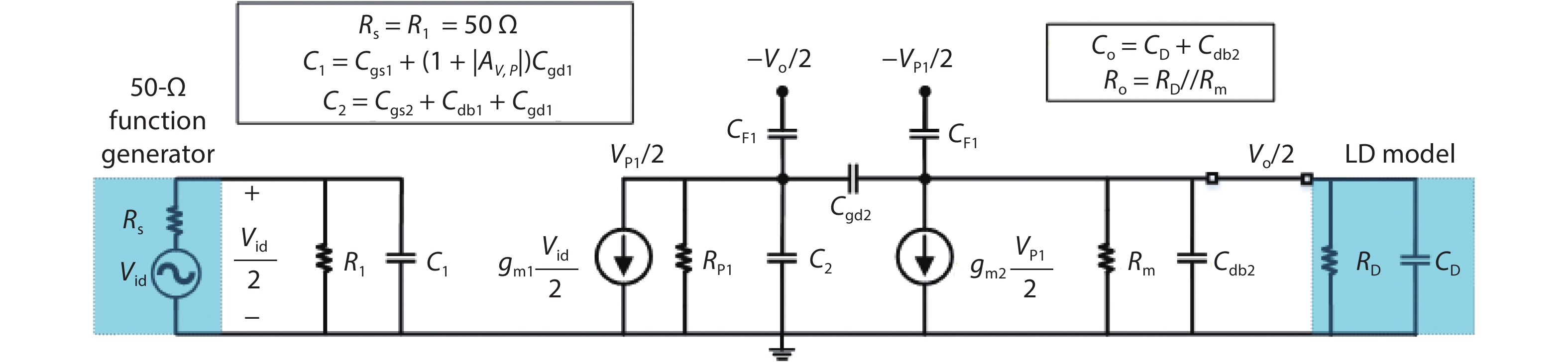
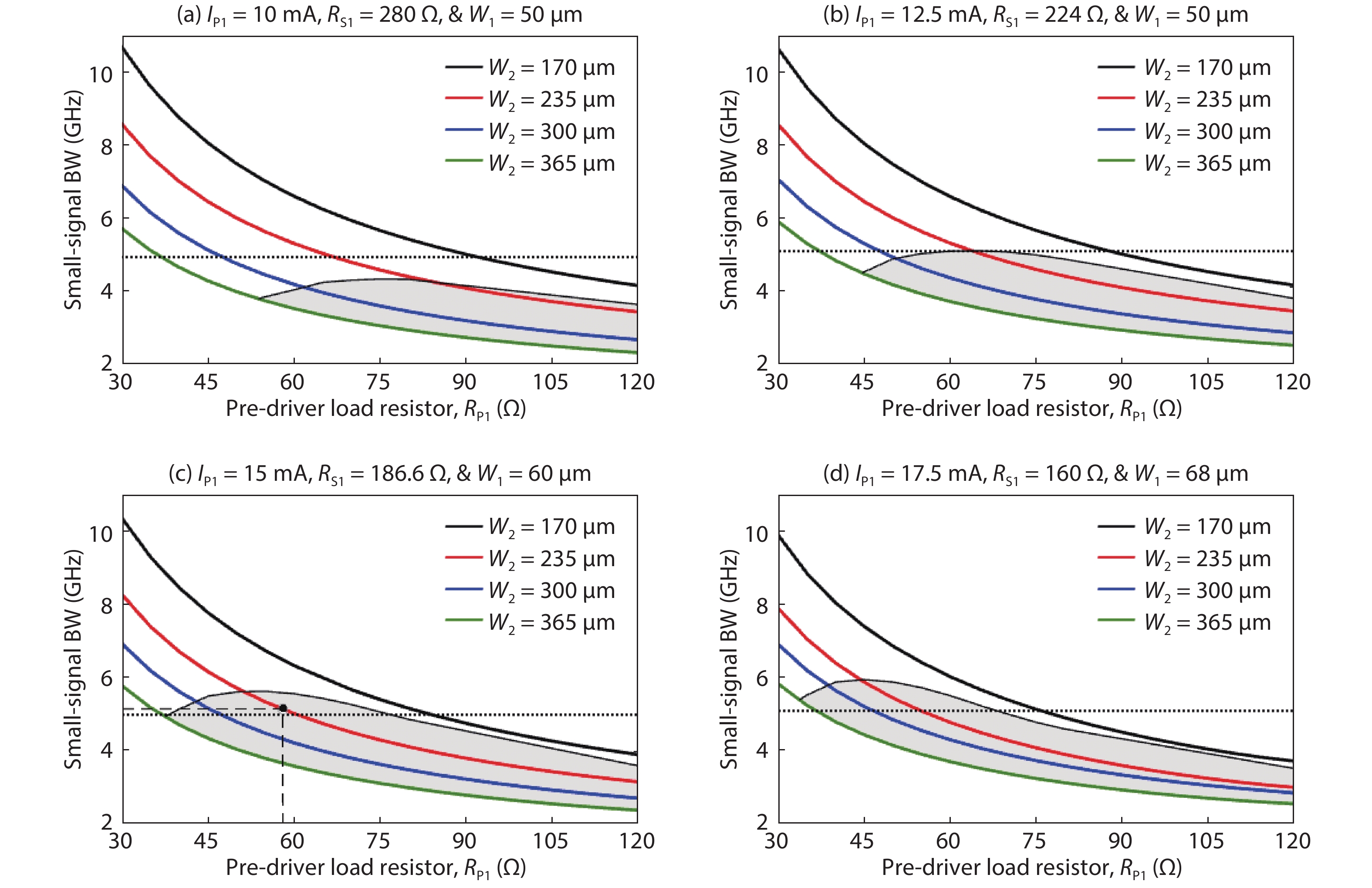
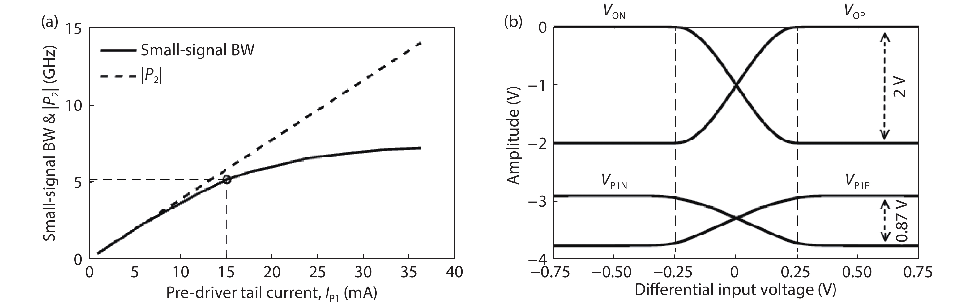
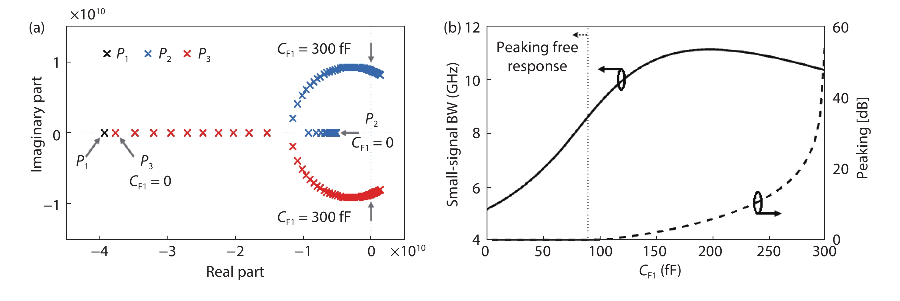
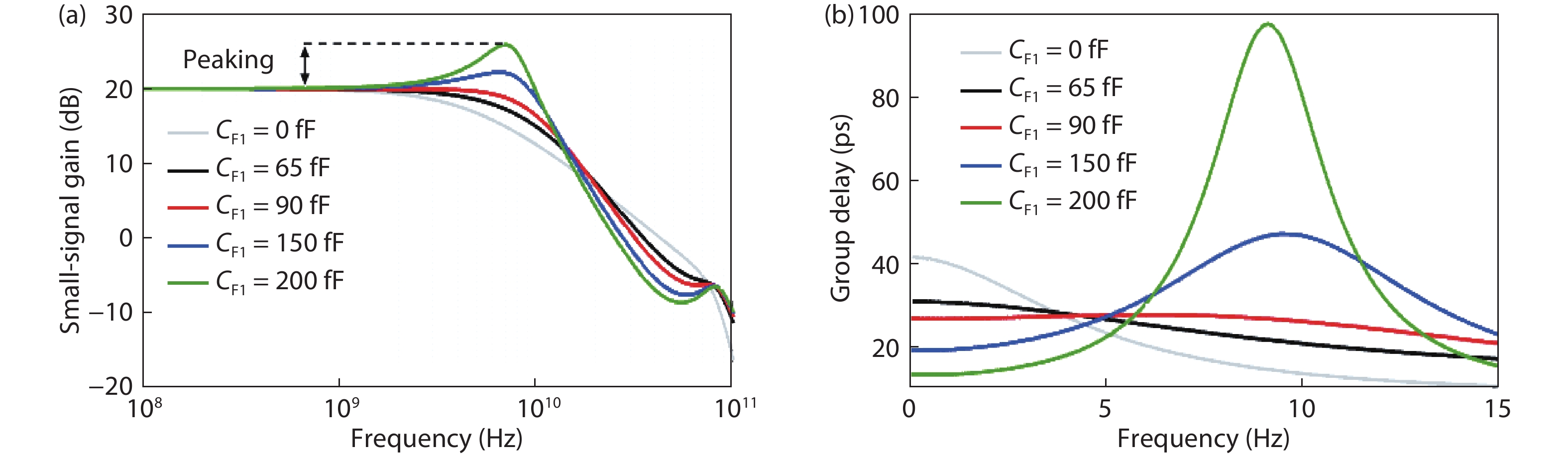
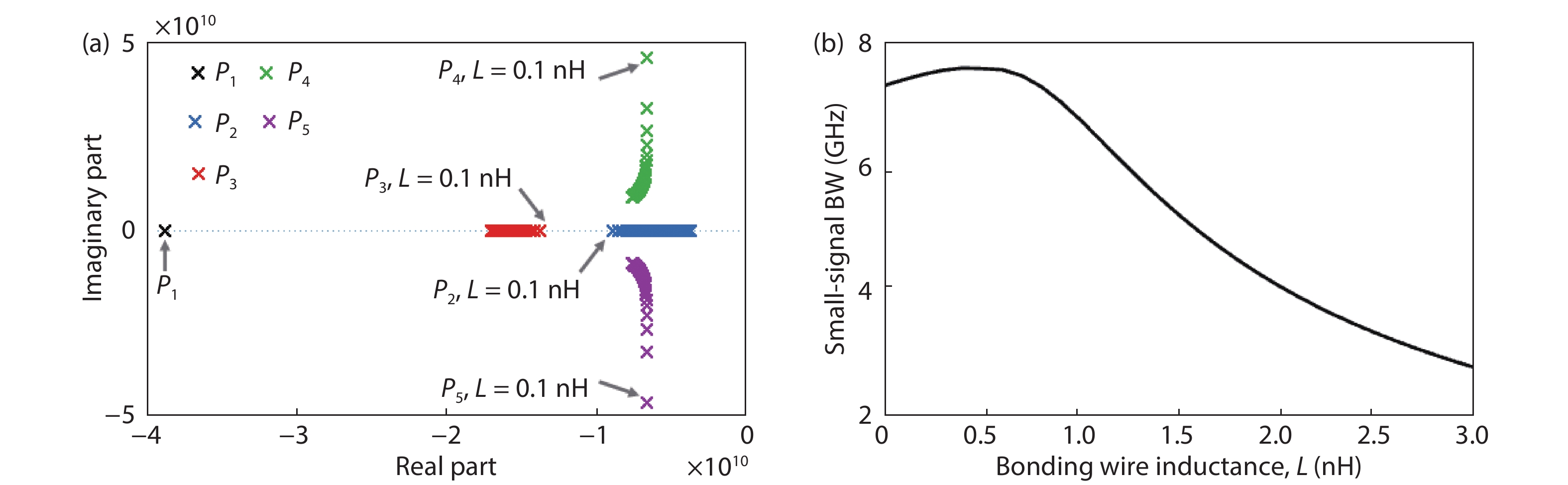
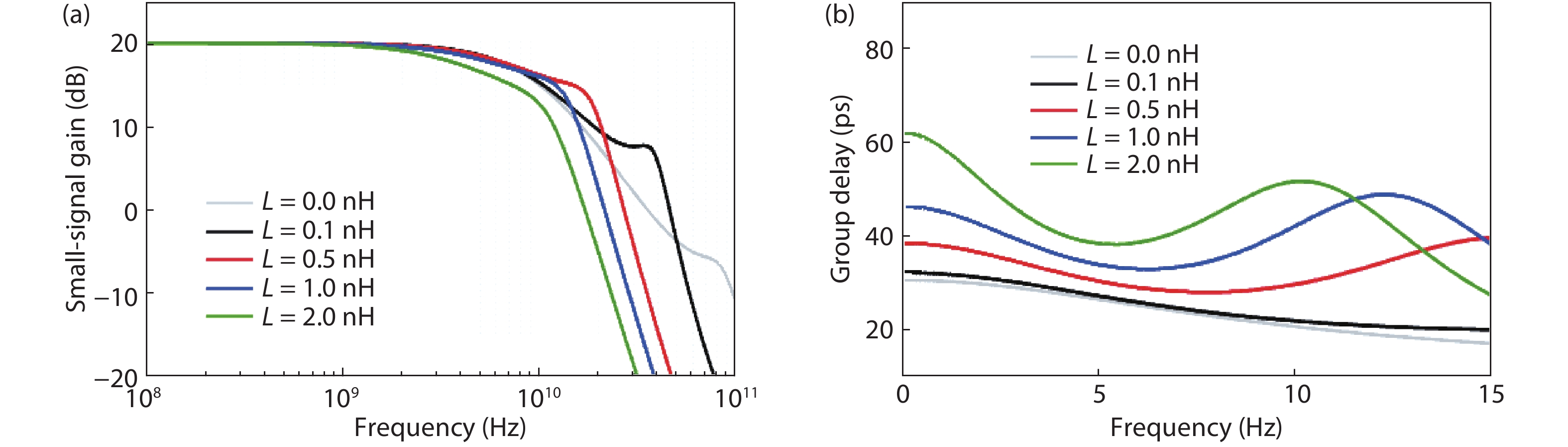
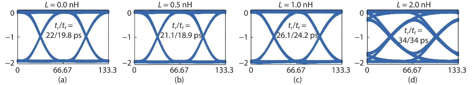
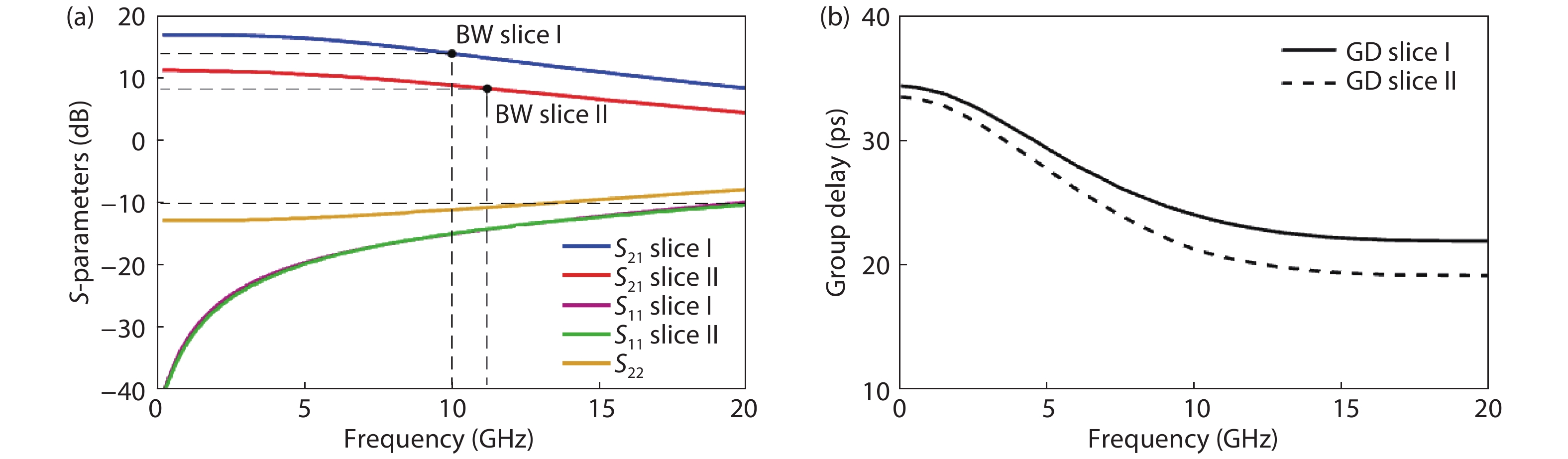
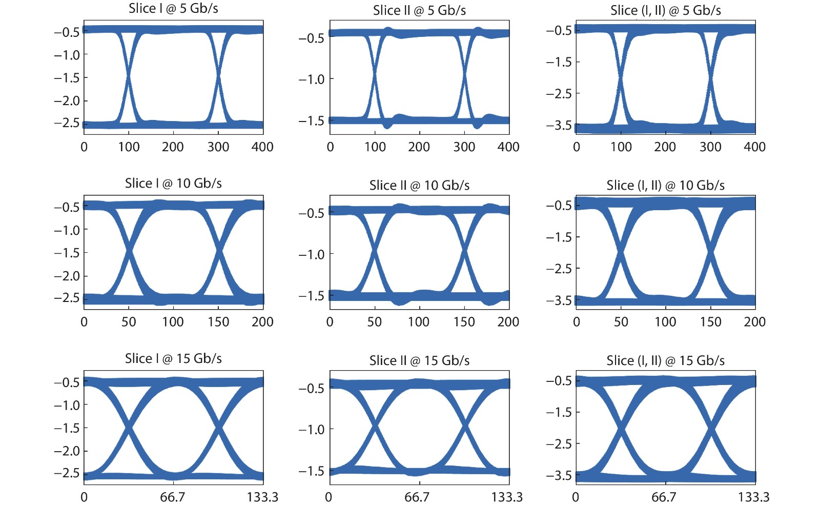
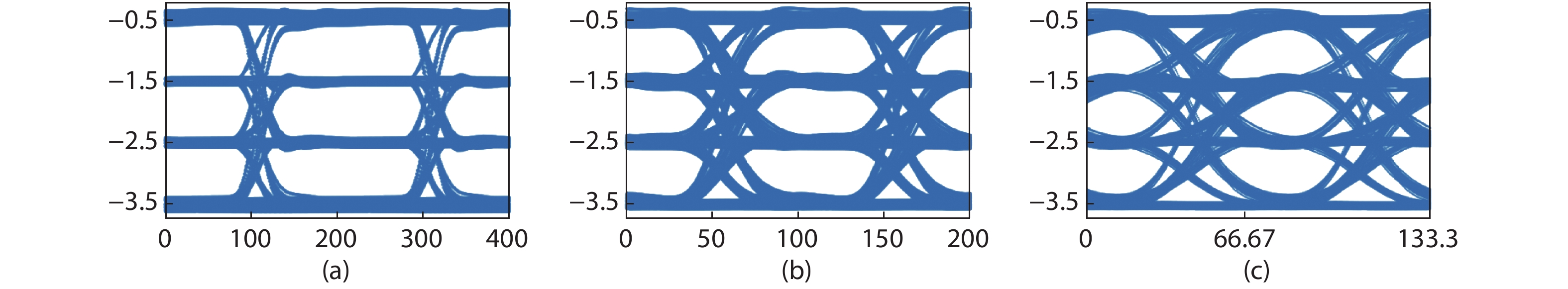
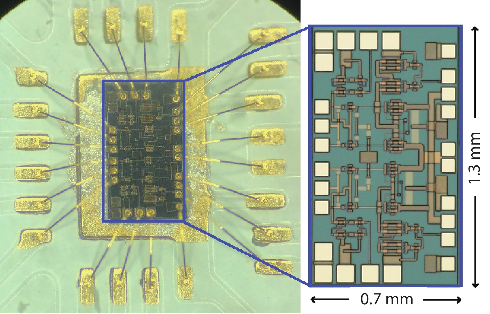
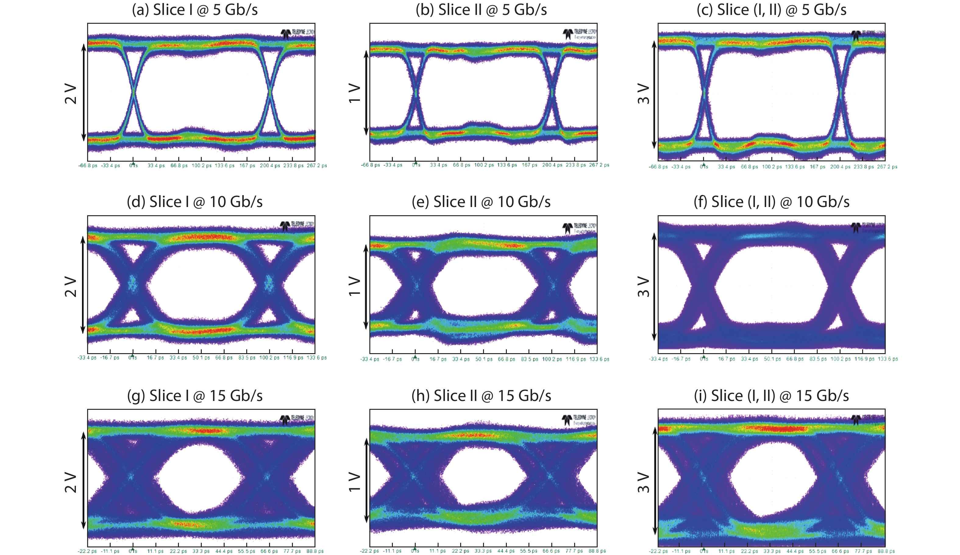
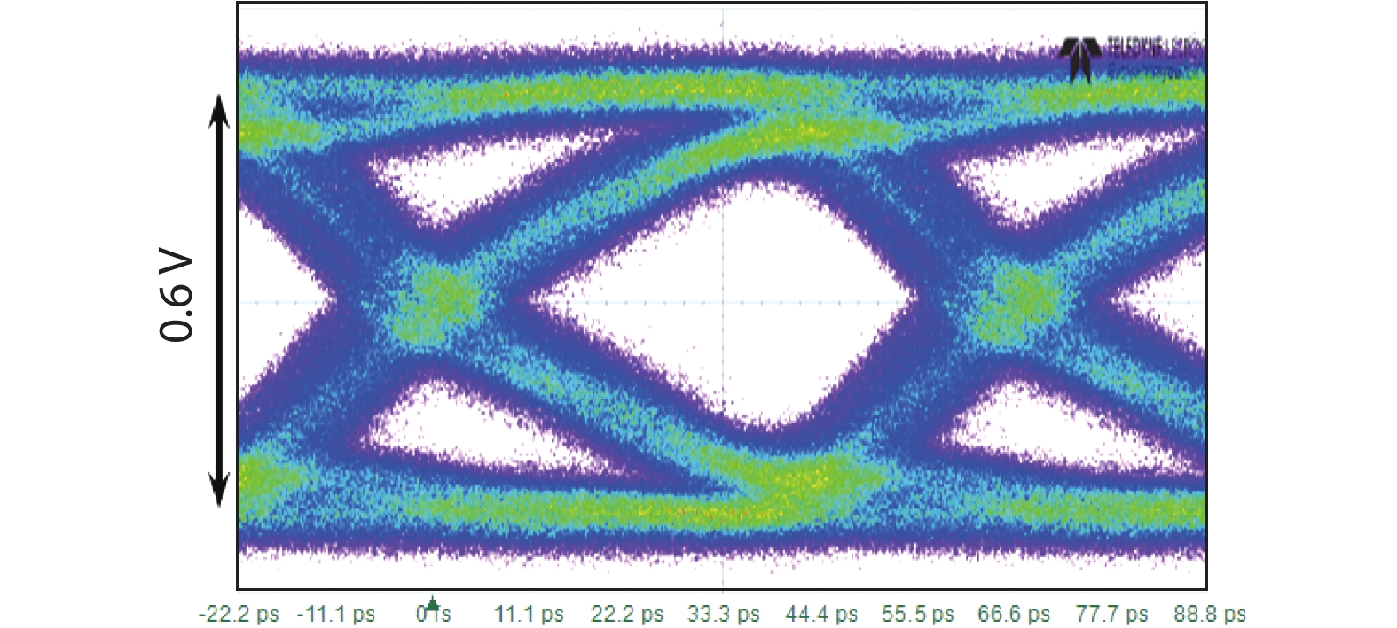
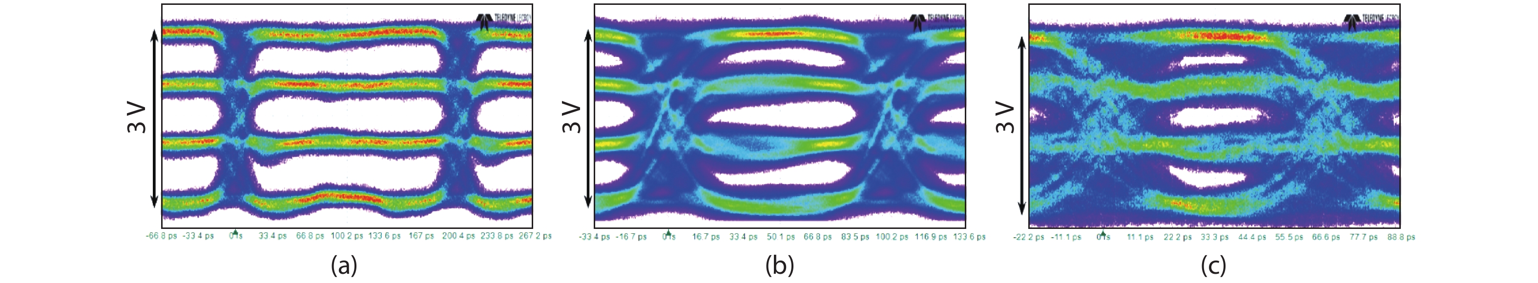
This paper presents the design and testing of a 15 Gbps non-return-to-zero (NRZ), 30 Gbps 4-level pulse amplitude modulation (PAM4) configurable laser diode driver (LDD) implemented in 0.15-µm GaAs E-mode pHEMT technology. The driver bandwidth is enhanced by utilizing cross-coupled neutralization capacitors across the output stage. The output transmission-line back-termination, which absorbs signal reflections from the imperfectly matched load, is performed passively with on-chip 50-Ω resistors. The proposed 30 Gbps PAM4 LDD is implemented by combining two 15 Gbps-NRZ LDDs, as the high and low amplification paths, to generate PAM4 output current signal with levels of 0, 40, 80, and 120 mA when driving 25-Ω lasers. The high and low amplification paths can be used separately or simultaneously as a 15 Gbps-NRZ LDD. The measurement results show clear output eye diagrams at speeds of up to 15 and 30 Gbps for the NRZ and PAM4 drivers, respectively. At a maximum output current of 120 mA, the driver consumes 1.228 W from a single supply voltage of –5.2 V. The proposed driver shows a high current driving capability with a better output power to power dissipation ratio, which makes it suitable for driving high current distributed feedback (DFB) lasers. The chip occupies a total area of 0.7 × 1.3 mm2.


J. Semicond.
2021, 42(7): 072501 doi: 10.1088/1674-4926/42/7/072501
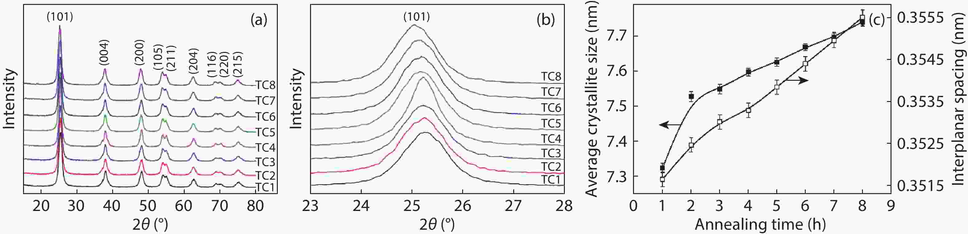
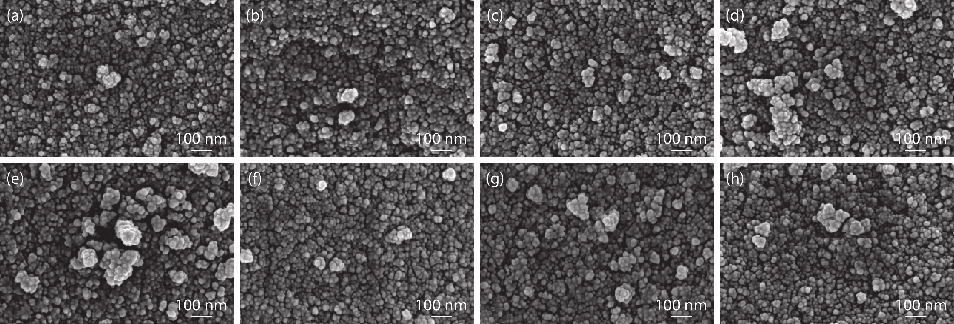
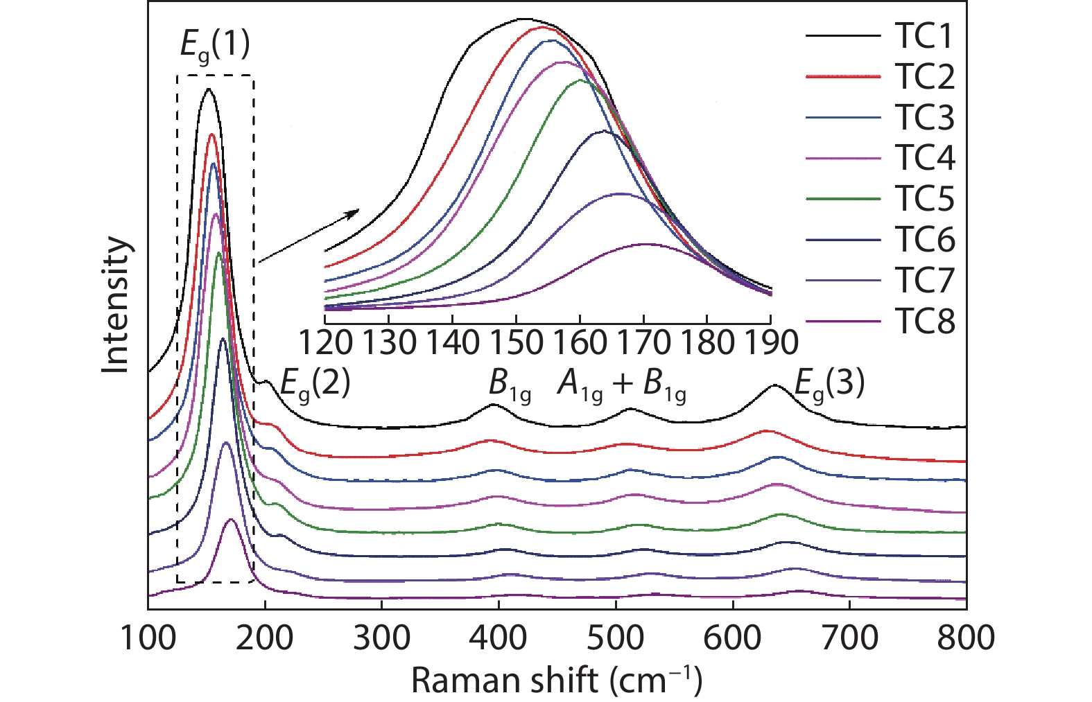
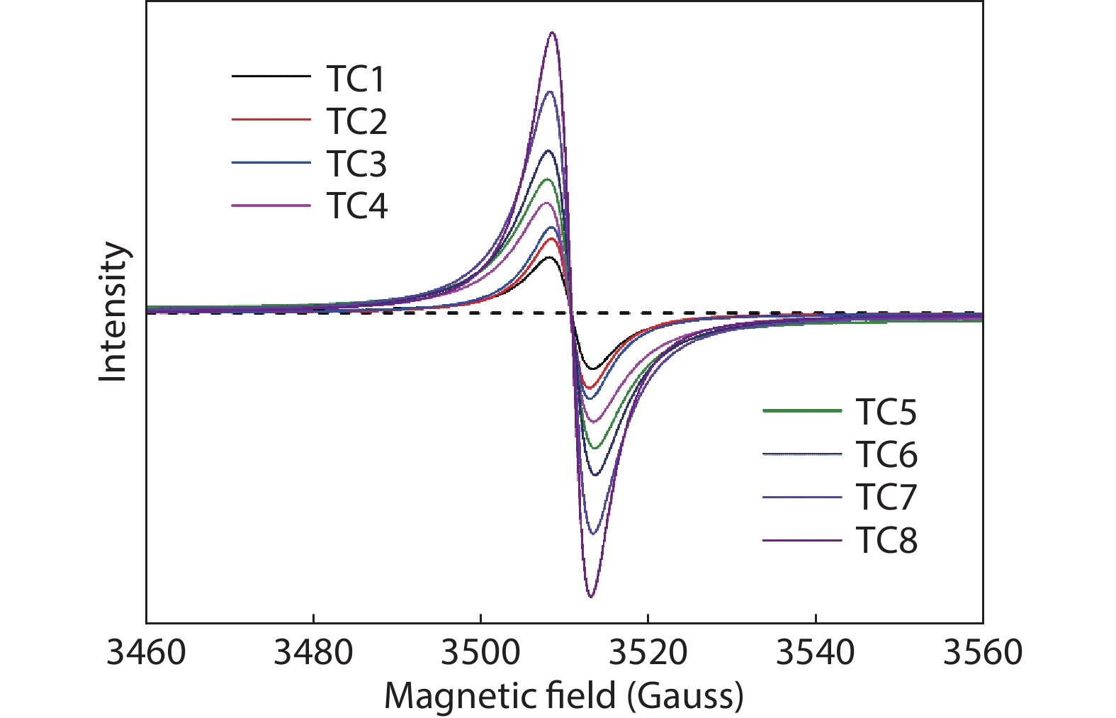
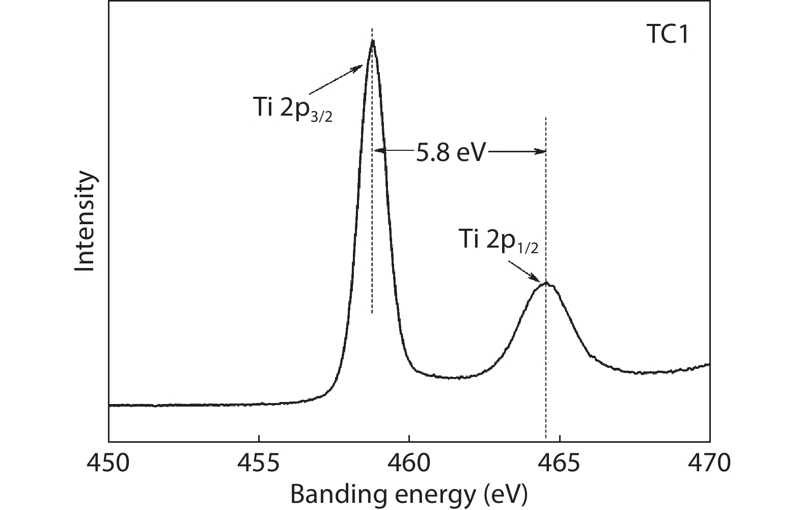
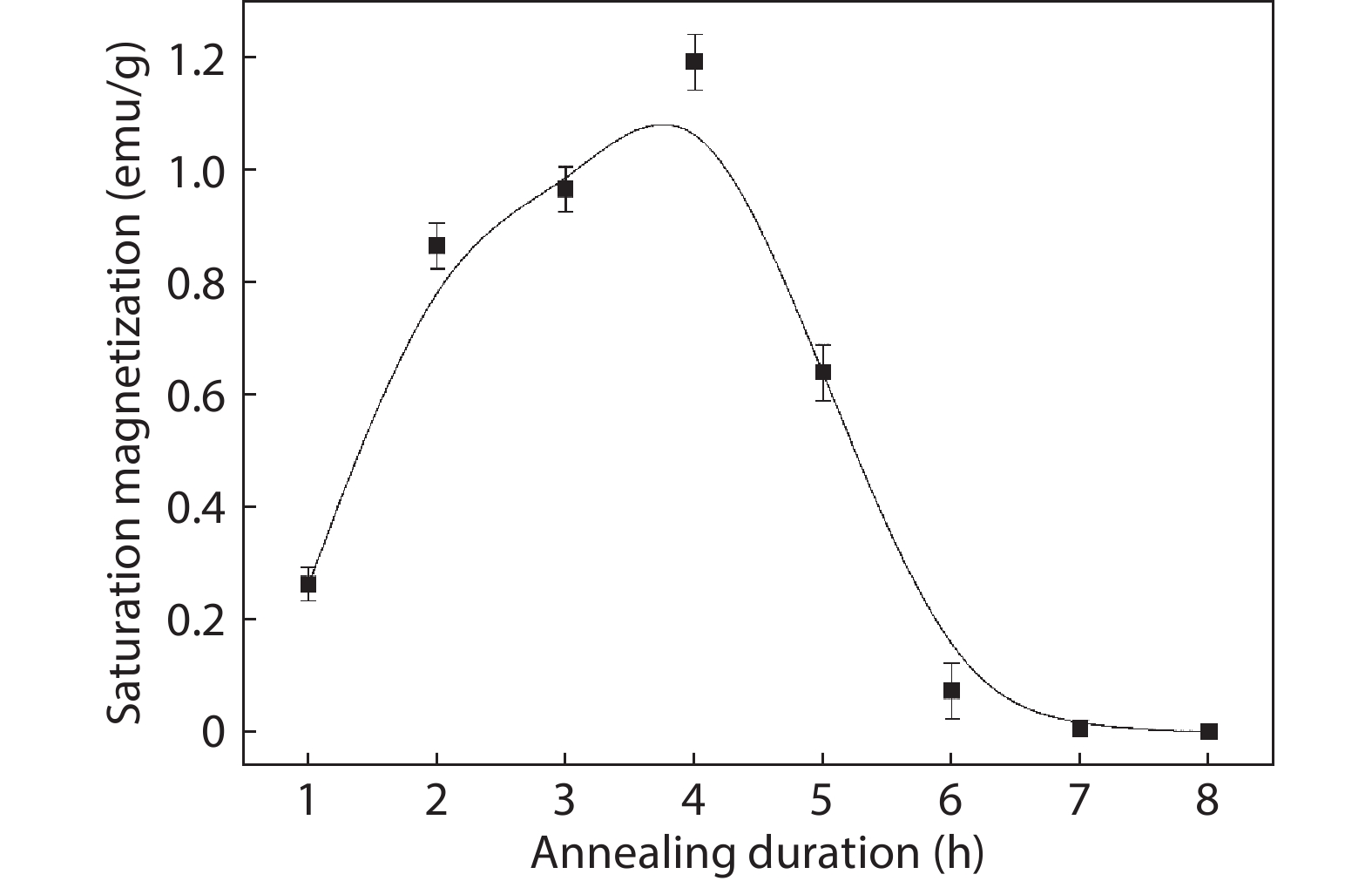
To clarify the contribution of oxygen vacancies to room-temperature ferromagnetism (RTFM) in cobalt doped TiO2 (Co-TiO2), and in order to obtain the high level of magnetization suitable for spintronic devices, in this work, Co-TiO2 nanoparticles are prepared via the sol–gel route, followed by vacuum annealing for different durations, and the influence of vacuum annealing duration on the structure and room-temperature magnetism of the compounds is examined. The results reveal that with an increase in annealing duration, the concentration of oxygen vacancies rises steadily, while the saturation magnetization (Ms) shows an initial gradual increase, followed by a sharp decline, and even disappearance. The maximum Ms is as high as 1.19 emu/g, which is promising with respect to the development of spintronic devices. Further analysis reveals that oxygen vacancies, modulated by annealing duration, play a critical role in tuning room-temperature magnetism. An appropriate concentration of oxygen vacancies is beneficial in terms of promoting RTFM in Co-TiO2. However, excessive oxygen vacancies will result in a negative impact on RTFM, due to antiferromagnetic superexchange interactions originating from nearest-neighbor Co2+ ions.


J. Semicond.
2021, 42(7): 072701 doi: 10.1088/1674-4926/42/7/072701
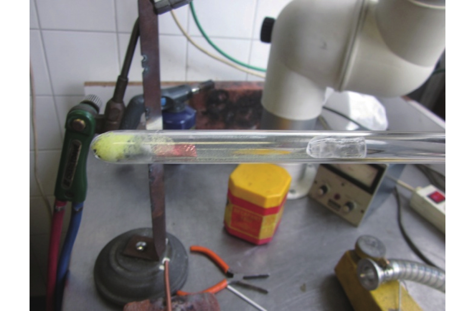
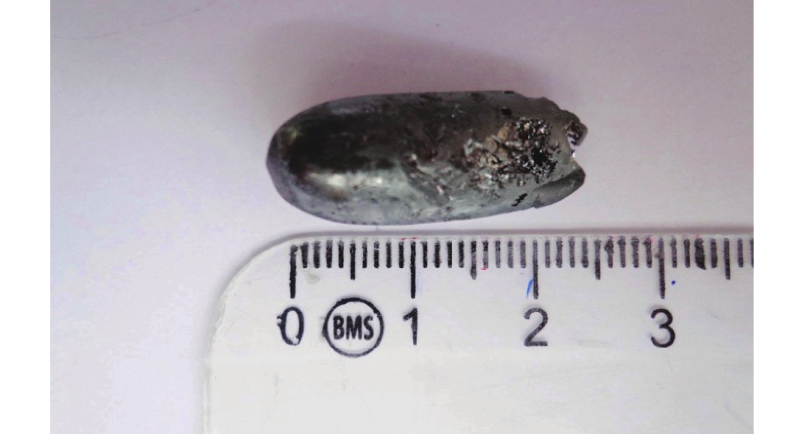
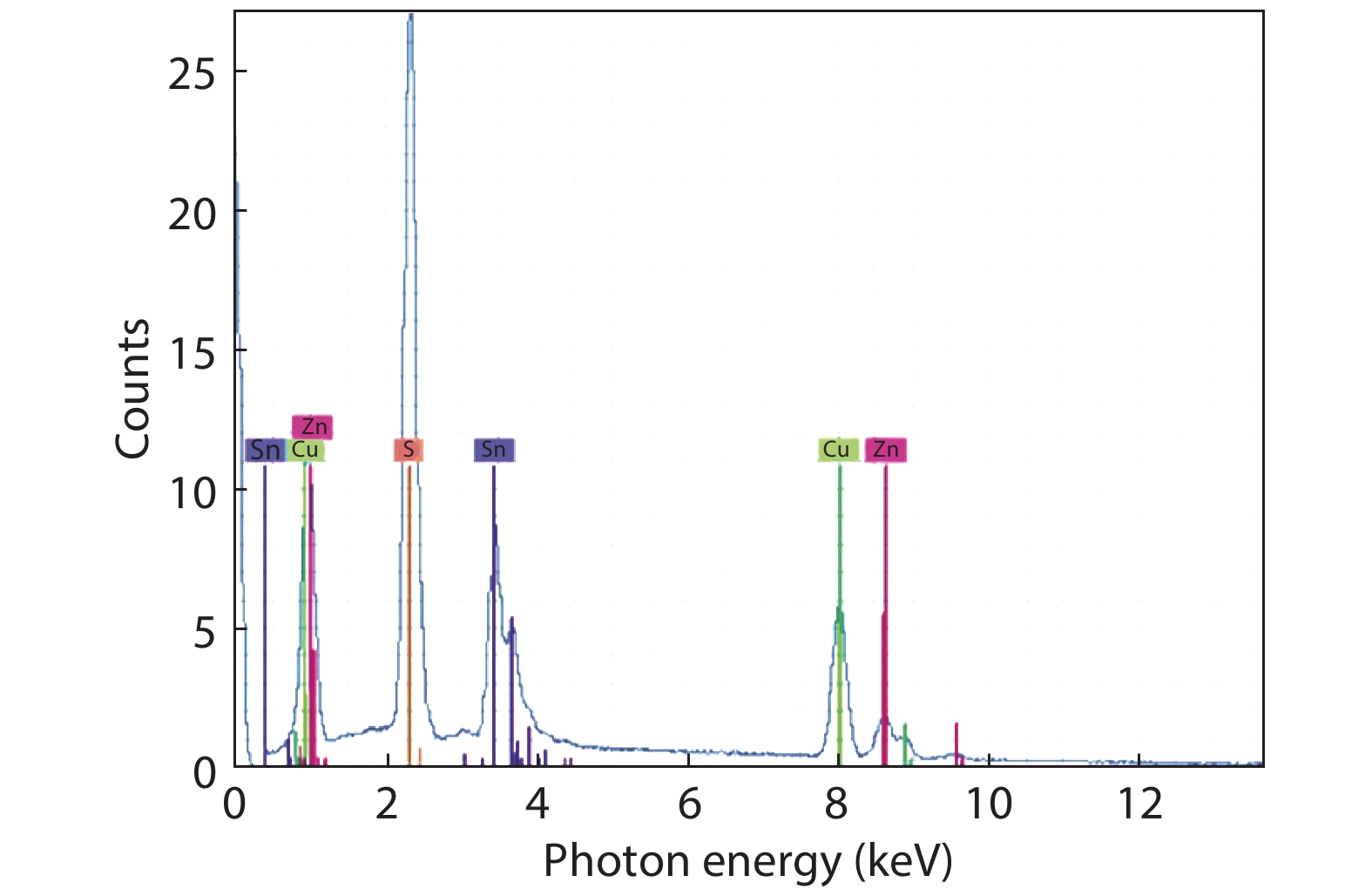
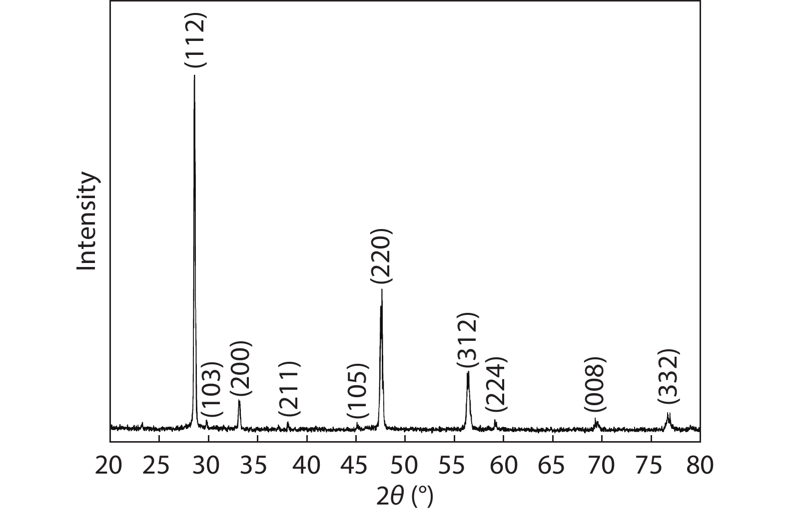
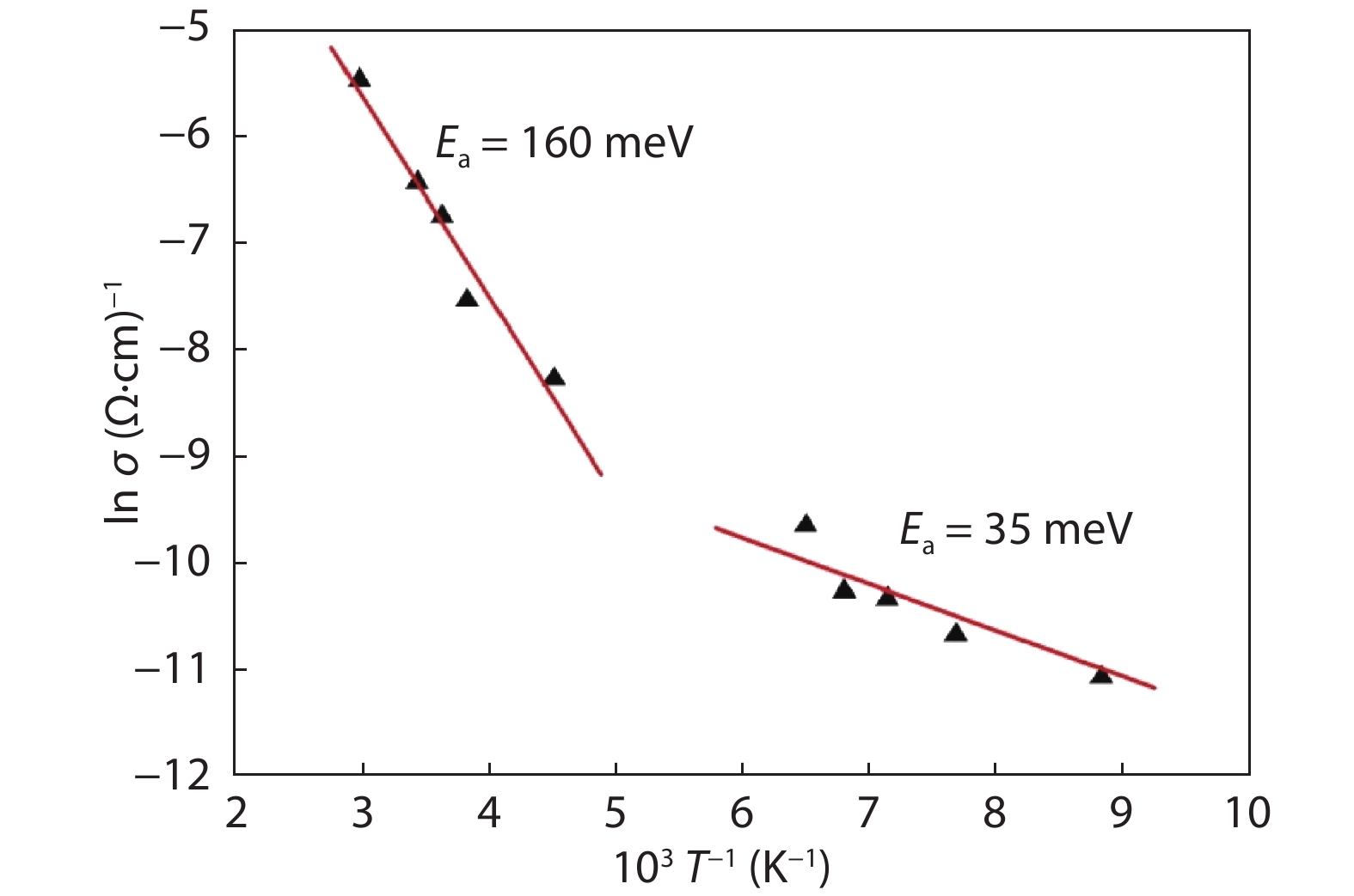
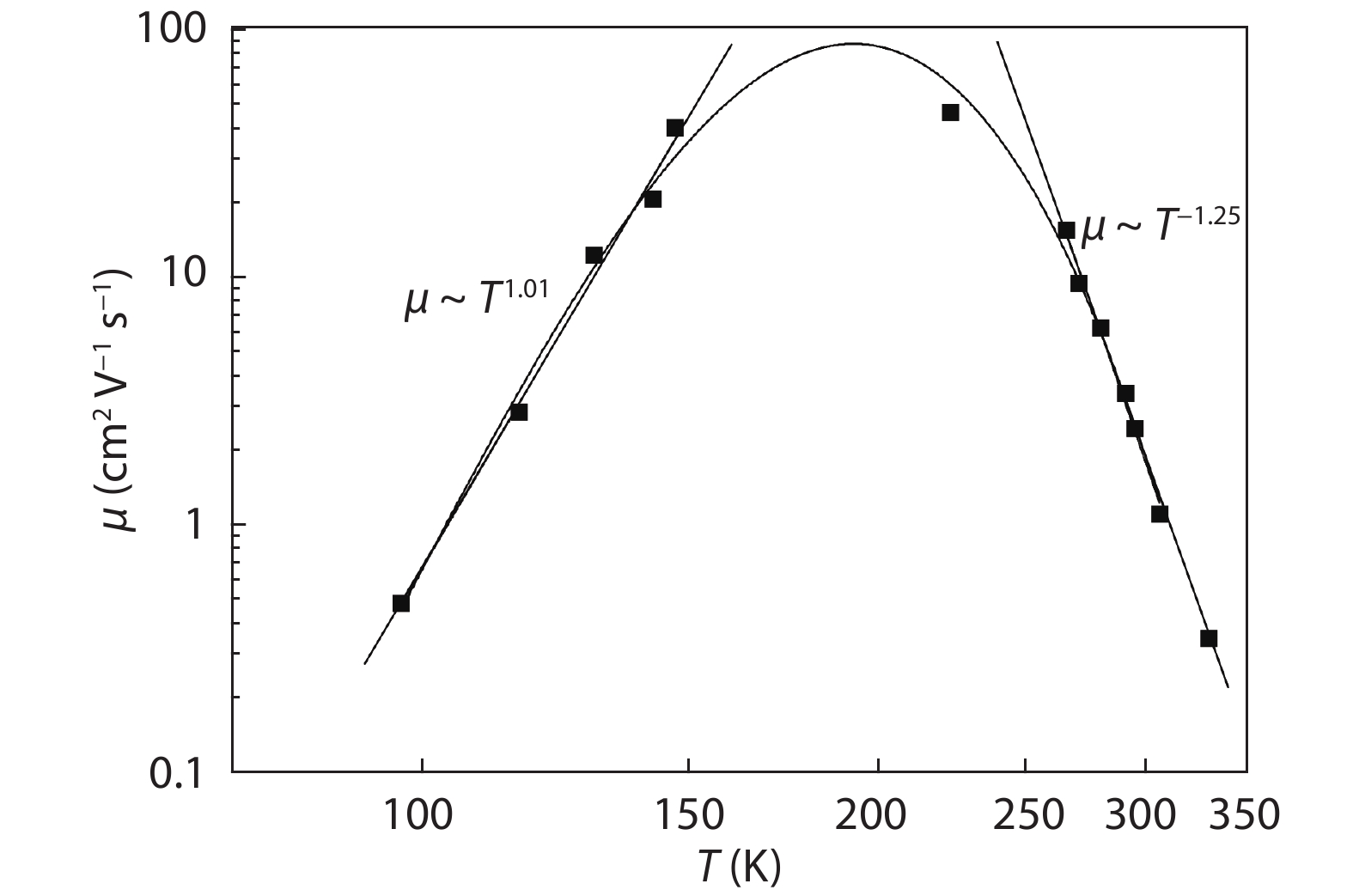
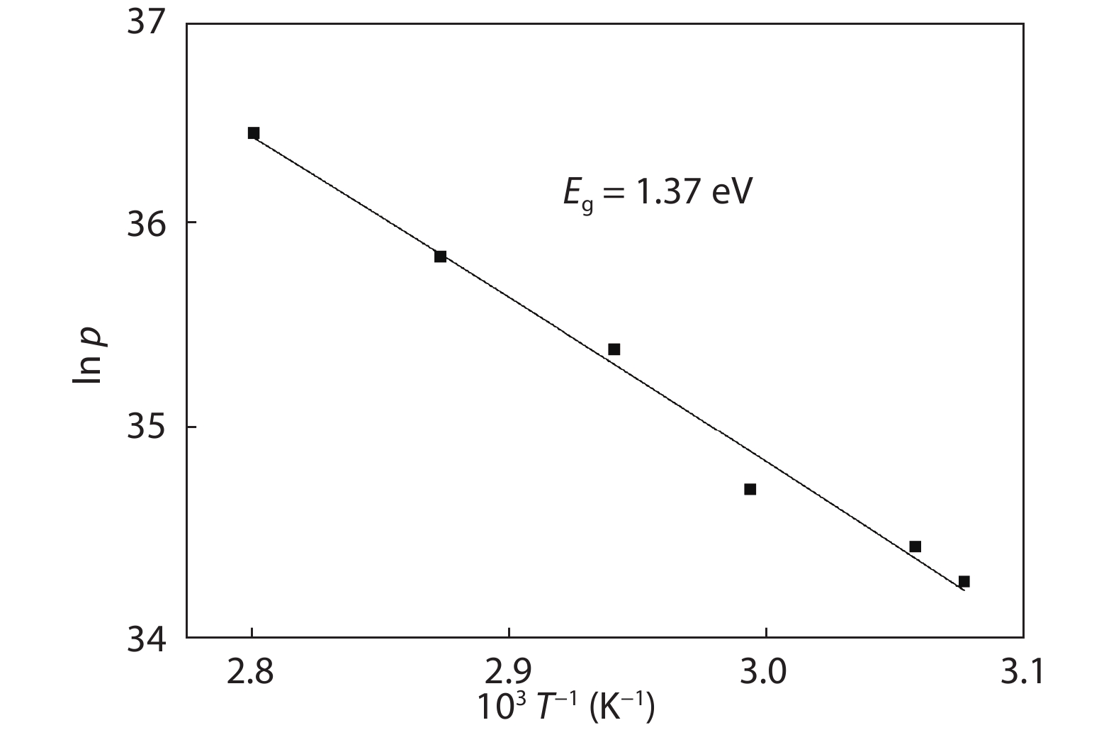
In this work, a Cu2ZnSnS4 (CZTS) ingot is grown via a melting method, then cooled; the resulting molten stoichiometric mixture is sealed off in a quartz ampoule under vacuum. The CZTS powder chemical composition analyses are determined using energy dispersive spectroscopy, and revealing the slightly Cu-rich and Zn-poor character of the ingot. Powder X-ray diffraction analysis reveals a crystalline structure with a kesterite phase formation, and a preferred orientation of (112) plane. The lattice constants of the a- and c- axes, calculated based on the XRD analyses, are a = 5.40 Å and c = 10.84 Å. Based on Hall measurements at room temperature, we find that the crystal exhibits p-type conductivity, with a high concentration of 1018 cm–3, a resistivity of 1.7 Ω cm, and a mobility of 10.69 cm2V–1s–1. Activation energies are estimated based on an Arrhenius plot of conductivity versus 1/T, for a temperature range of 80–350 K, measuring 35 and 160 meV in low- and high-temperature regimes, respectively, which is attributed to complex defects (2CuZn+SnZn) and antisite defects (CuZn), respectively. The observed scattering mechanisms are attributed to ionized impurities and acoustic phonons at low and high temperatures, respectively. The extracted band-gap is 1.37 eV.
J. Semicond.
2021, 42(7): 072901 doi: 10.1088/1674-4926/42/7/072901
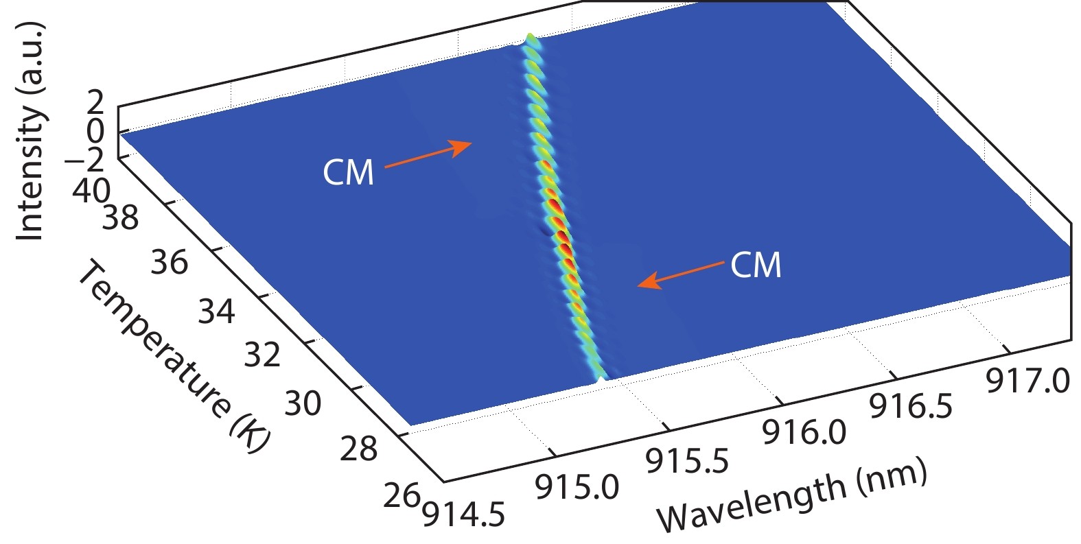
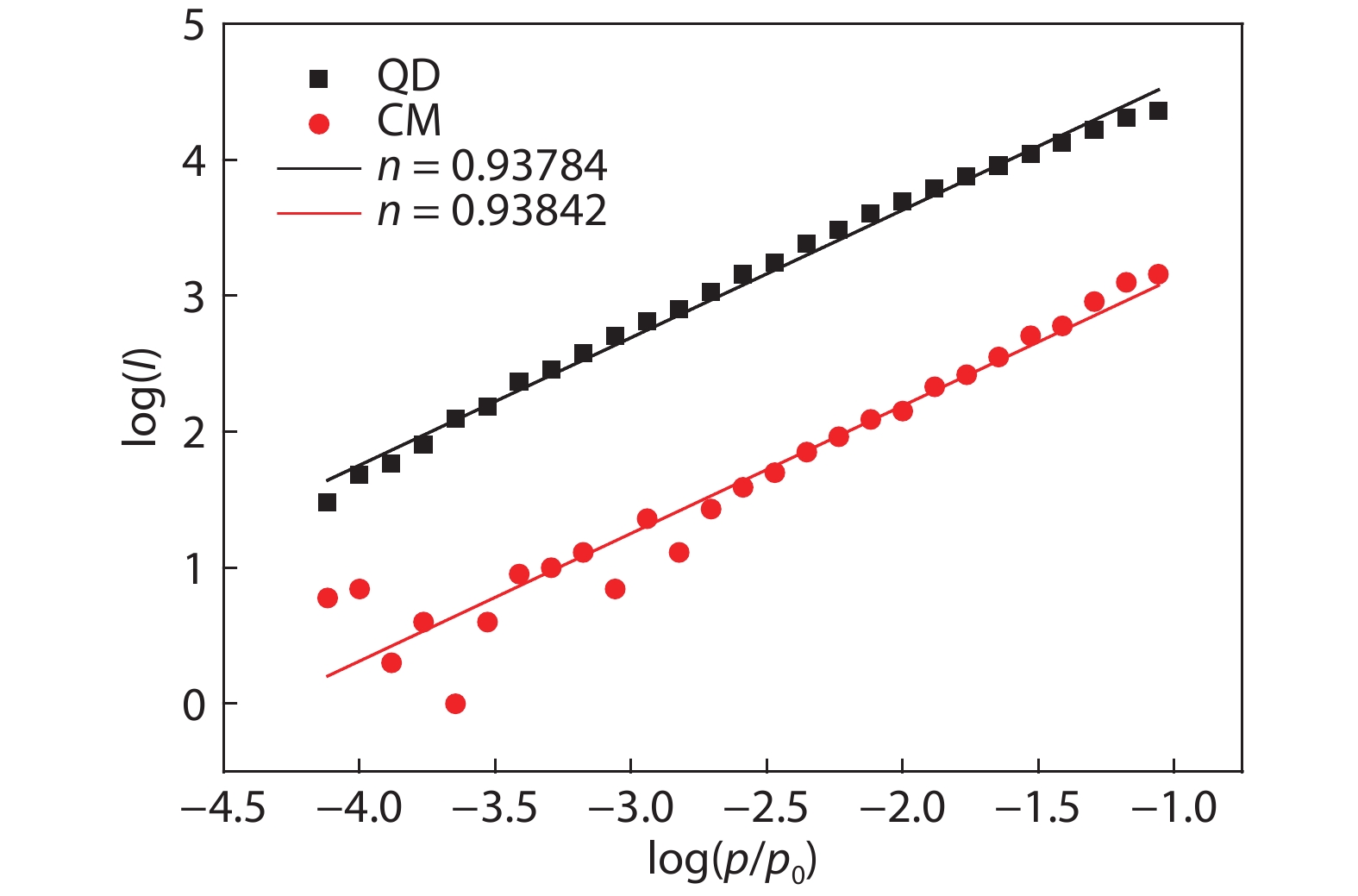
In this work, we achieve high count-rate single-photon output in single-mode (SM) optical fiber. Epitaxial and dilute InAs/GaAs quantum dots (QDs) are embedded in a GaAs/AlGaAs distributed Bragg reflector (DBR) with a micro-pillar cavity, so as to improve their light emission extraction in the vertical direction, thereby enhancing the optical SM fiber’s collection capability (numerical aperture: 0.13). By tuning the temperature precisely to make the quantum dot exciton emission resonant to the micro-pillar cavity mode (Q ~ 1800), we achieve a fiber-output single-photon count rate as high as 4.73 × 10⁶ counts per second, with the second-order auto-correlation g2(0) remaining at 0.08.


J. Semicond.
2021, 42(7): 074101 doi: 10.1088/1674-4926/42/7/074101
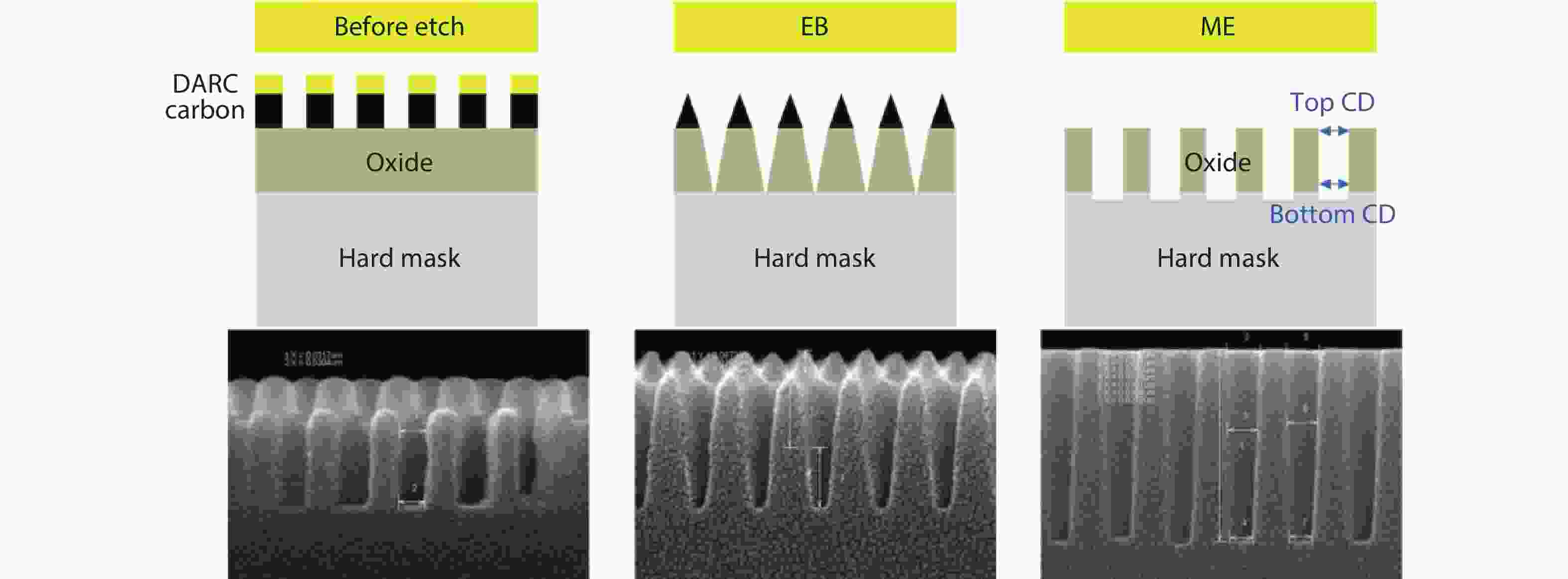
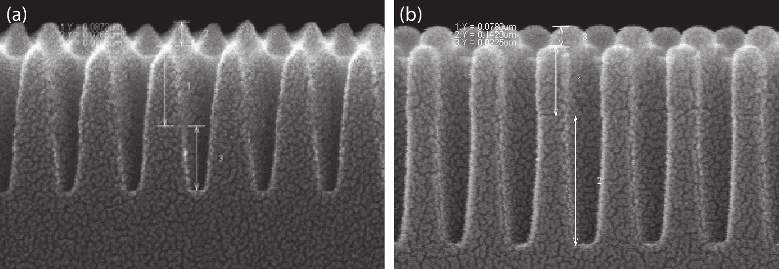
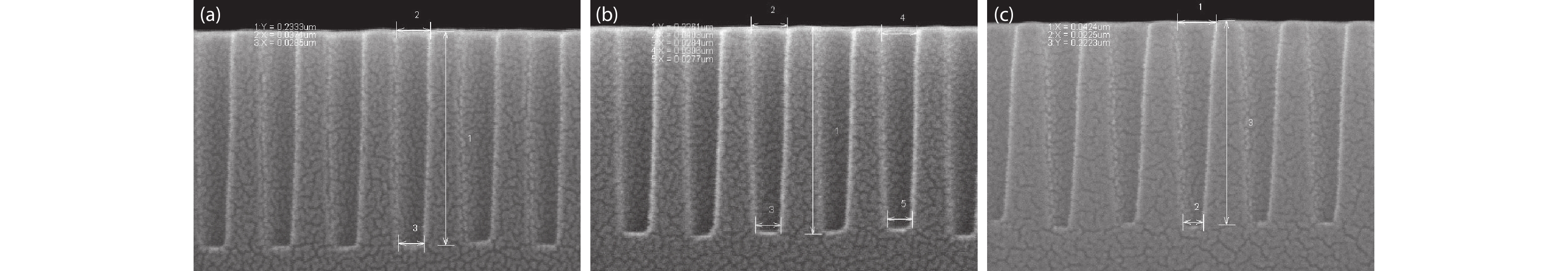
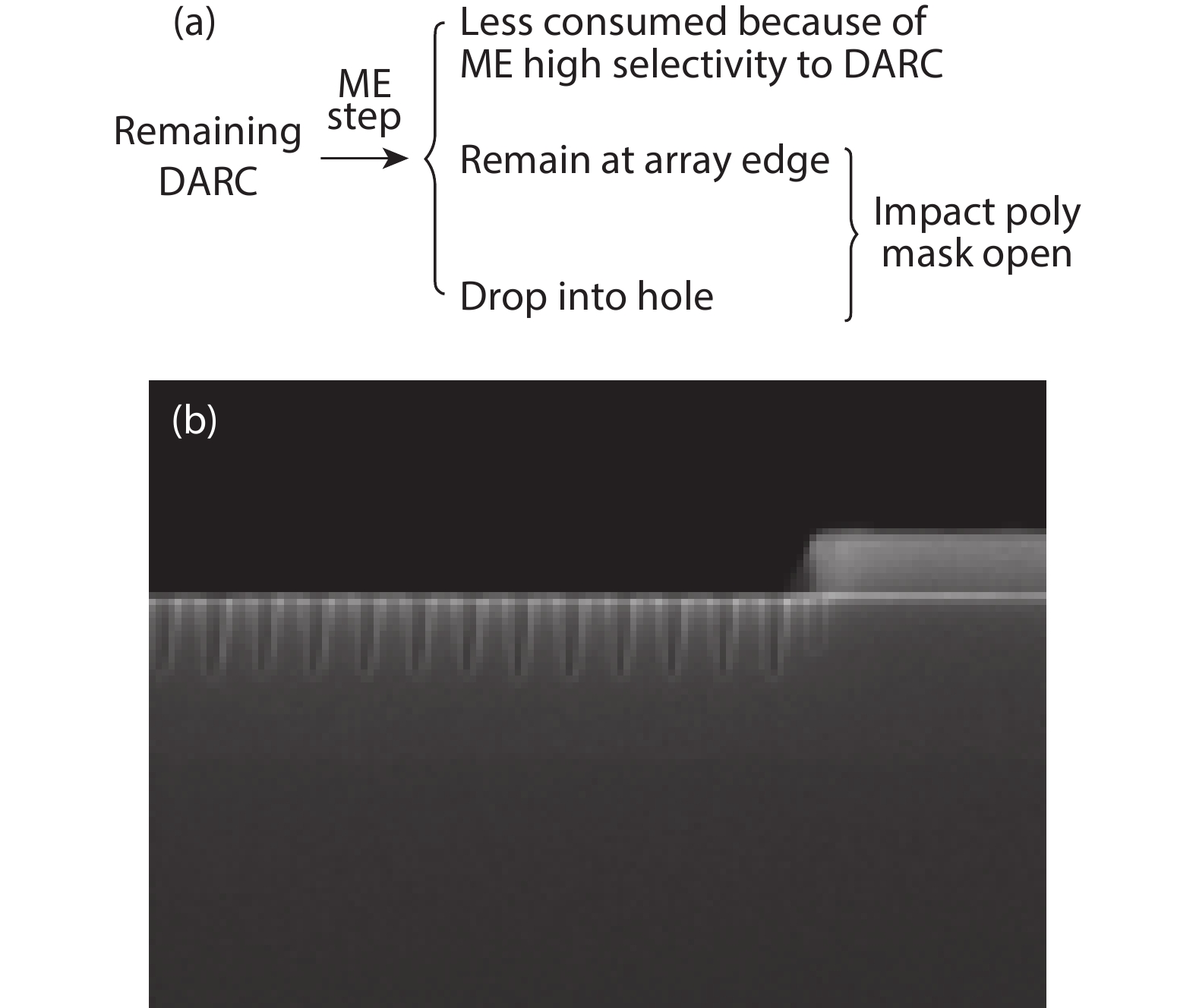
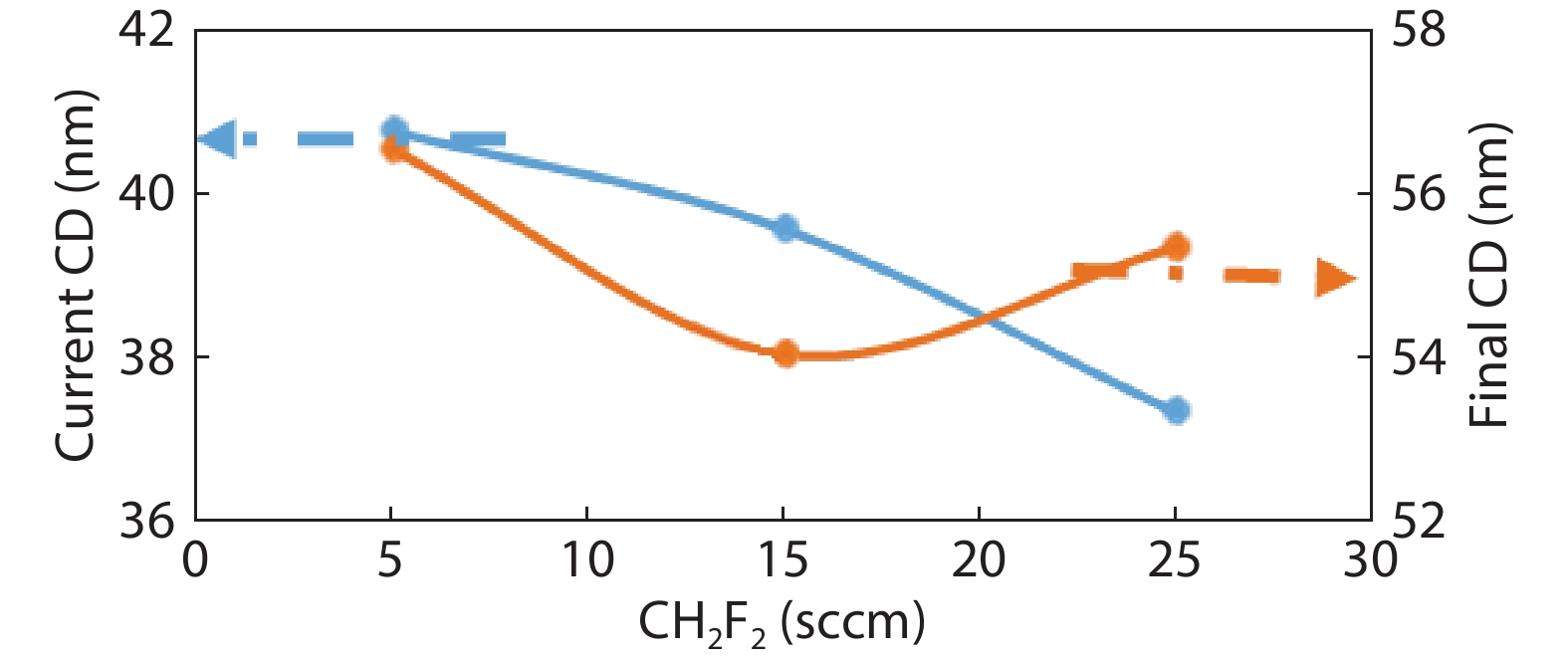
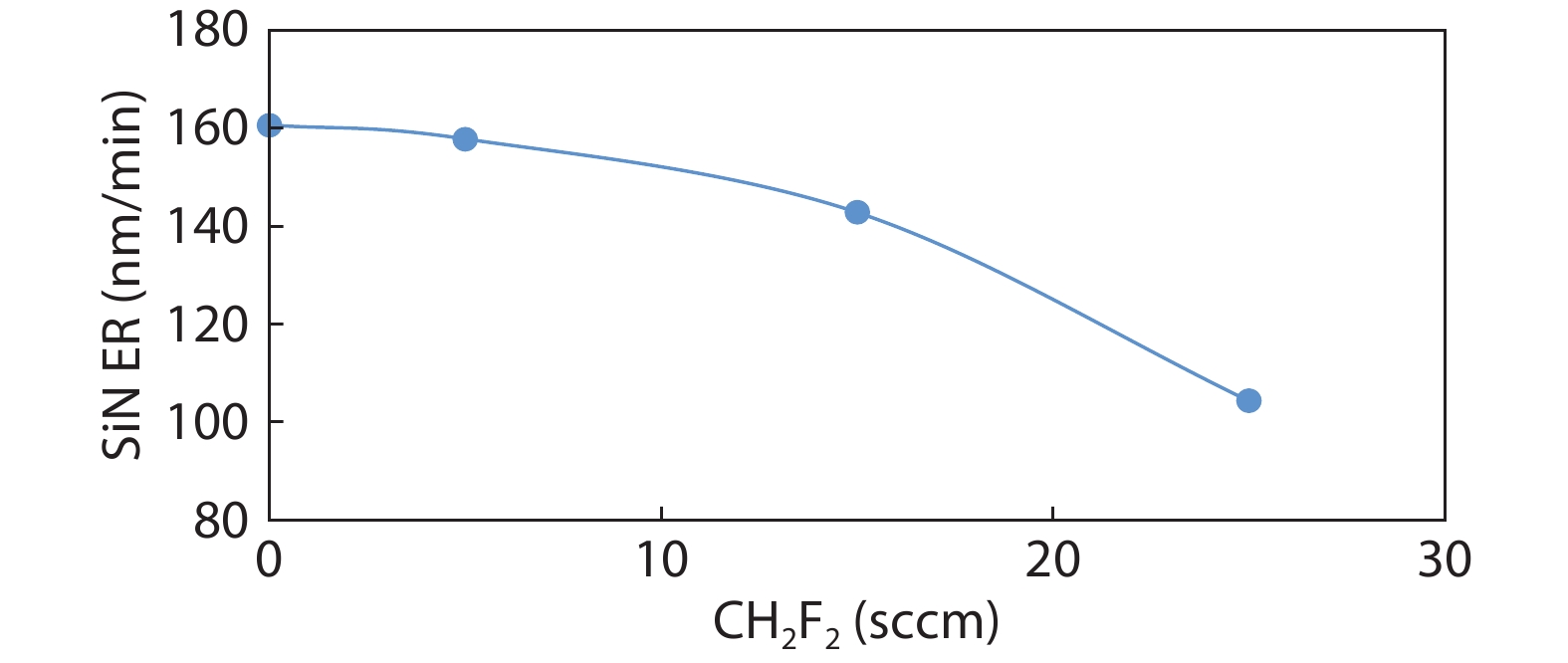
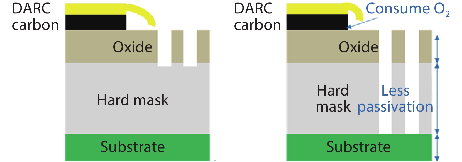
Opening the silicon oxide mask of a capacitor in dynamic random access memory is a critical process on a capacitive coupled plasma (CCP) etch tool. Three steps, dielectric anti-reflective coating (DARC) etch back, silicon oxide etch and strip, are contained. To acquire good performance, such as low leakage current and high capacitance, for further fabricating capacitors, we should firstly optimize DARC etch back. We developed some experiments, focusing on etch time and chemistry, to evaluate the profile of a silicon oxide mask, DARC remain and critical dimension. The result shows that etch back time should be controlled in the range from 50 to 60 s, based on the current equipment and condition. It will make B/T ratio higher than 70% meanwhile resolve the DARC remain issue. We also found that CH2F2 flow should be ~15 sccm to avoid reversed CD trend and keep inline CD.


J. Semicond.
2021, 42(7): 074102 doi: 10.1088/1674-4926/42/7/074102

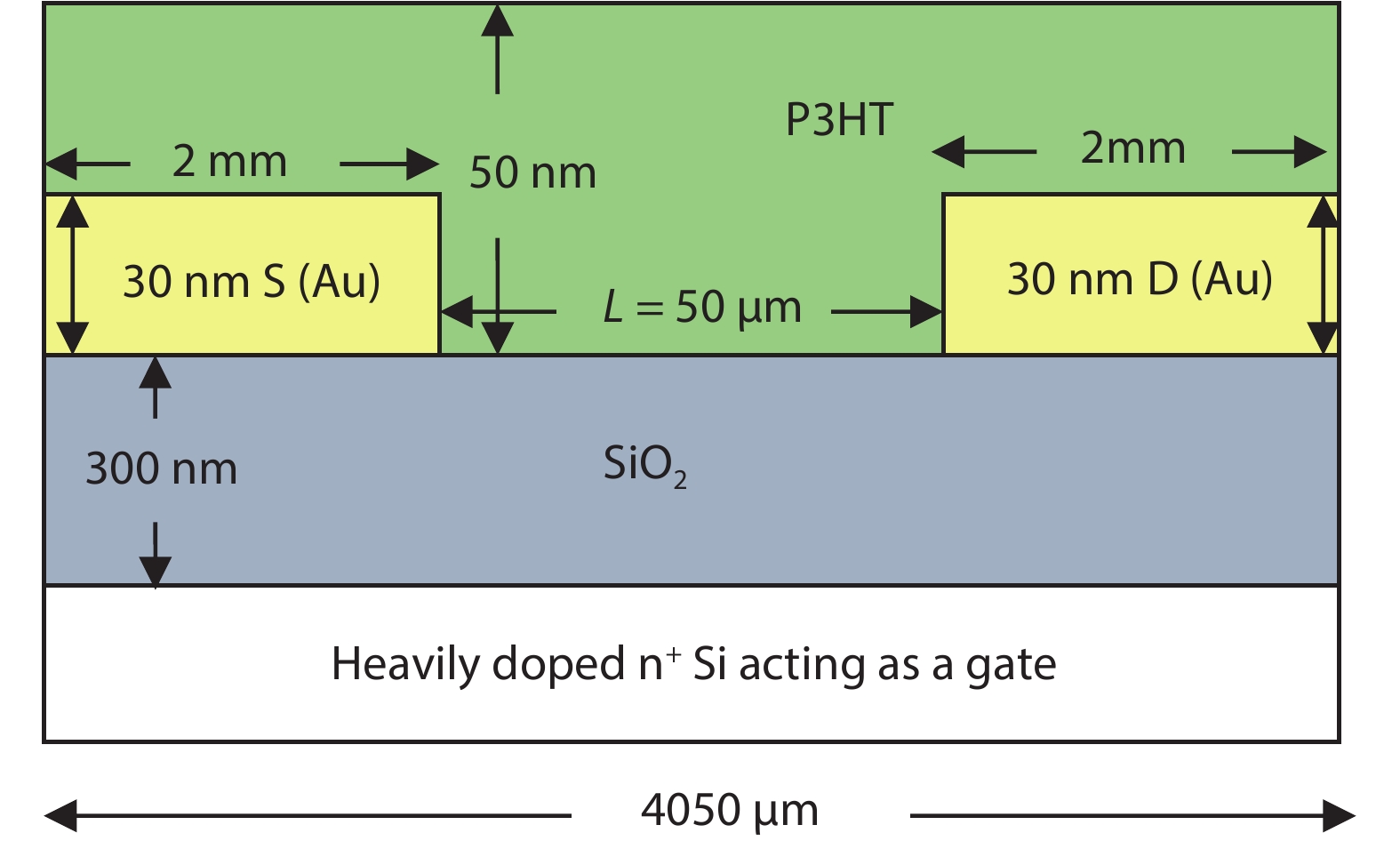
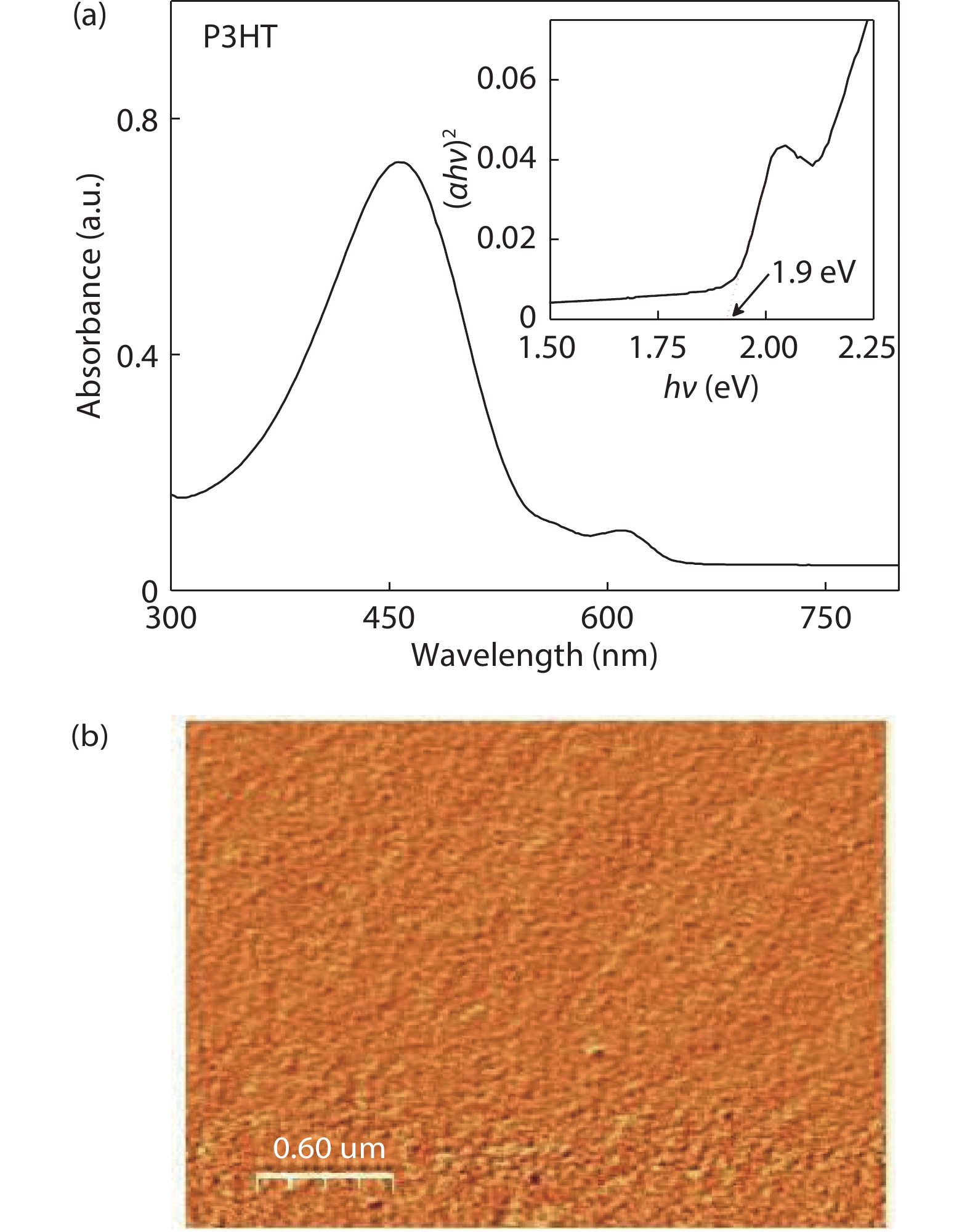
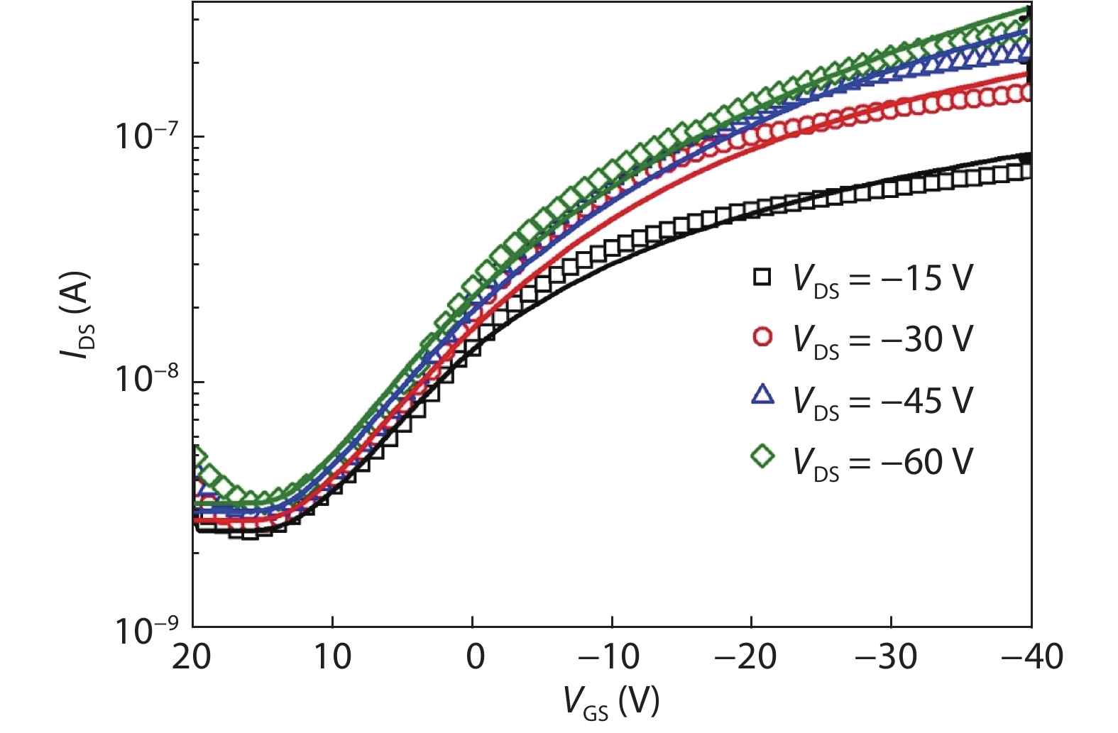
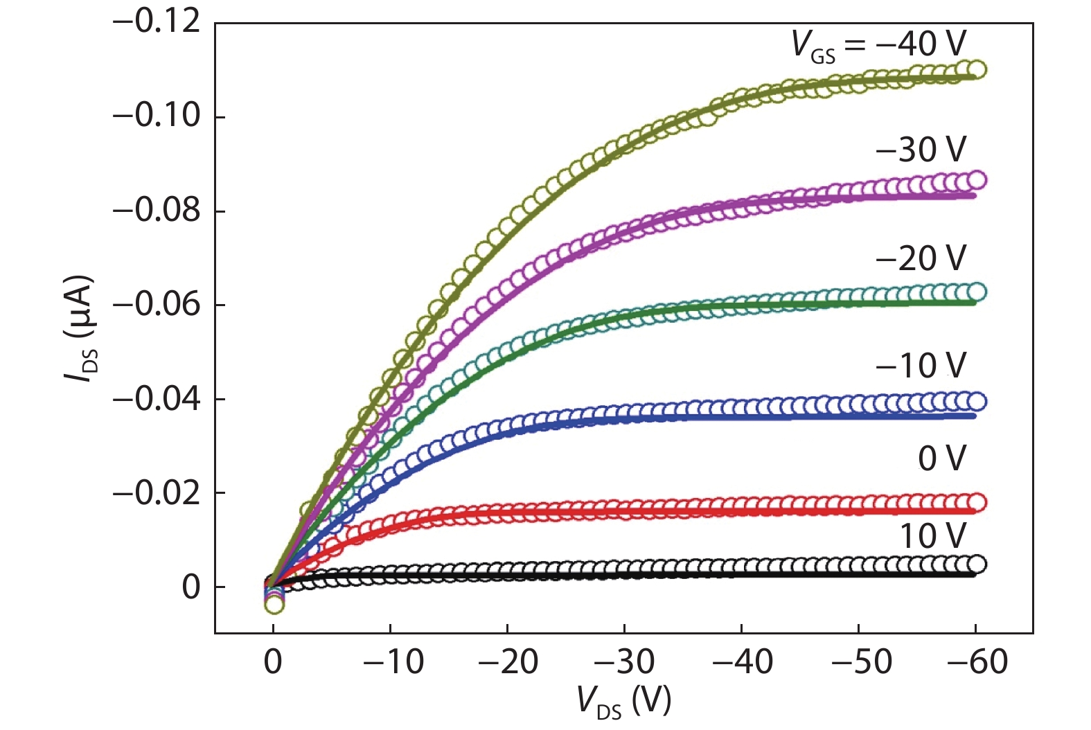
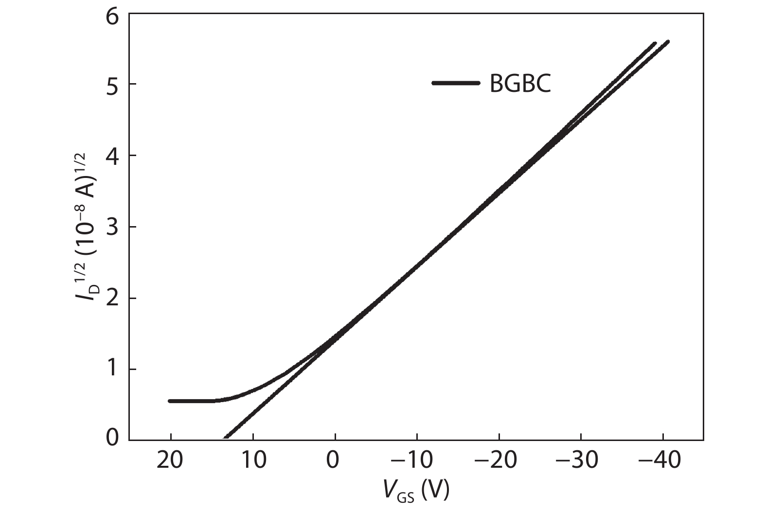
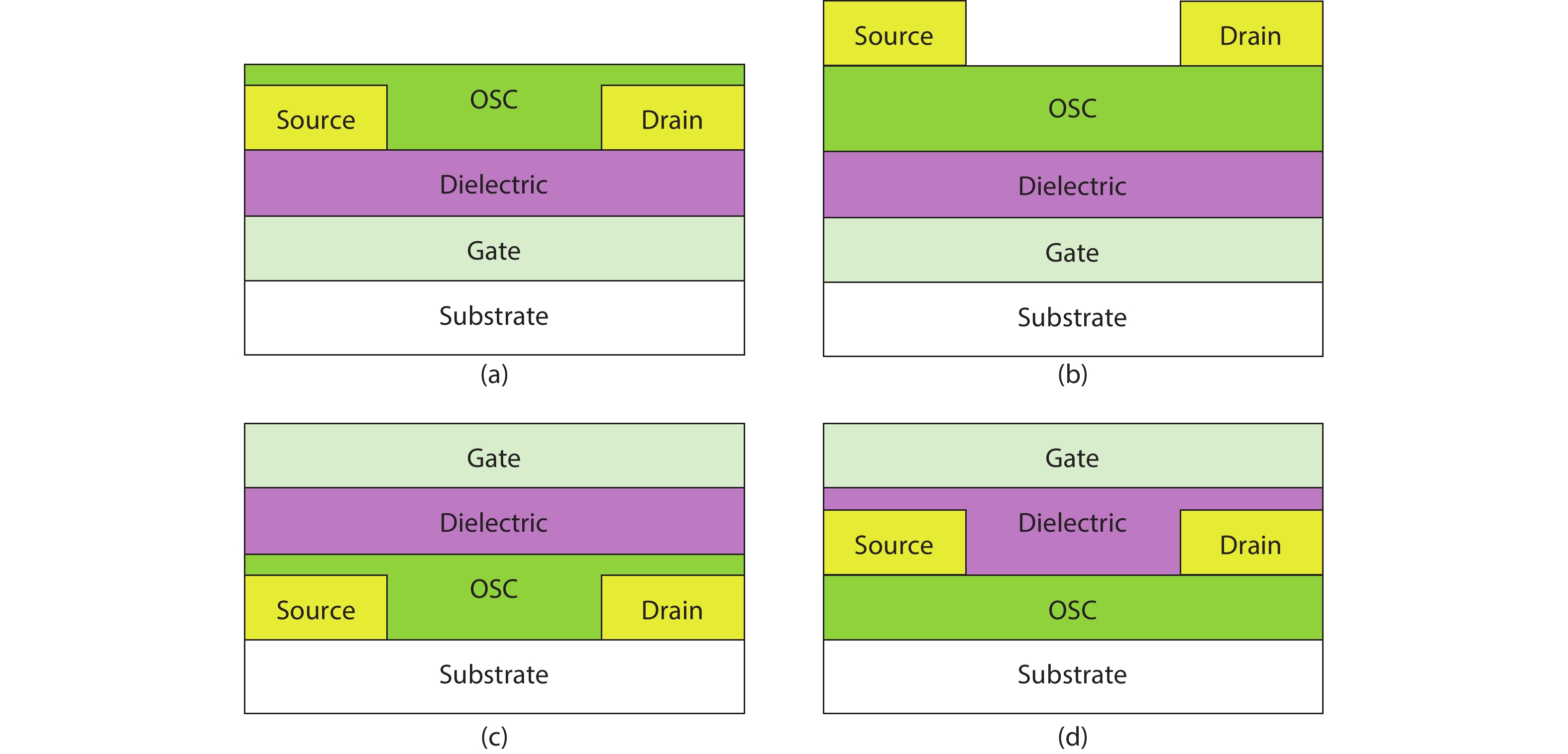
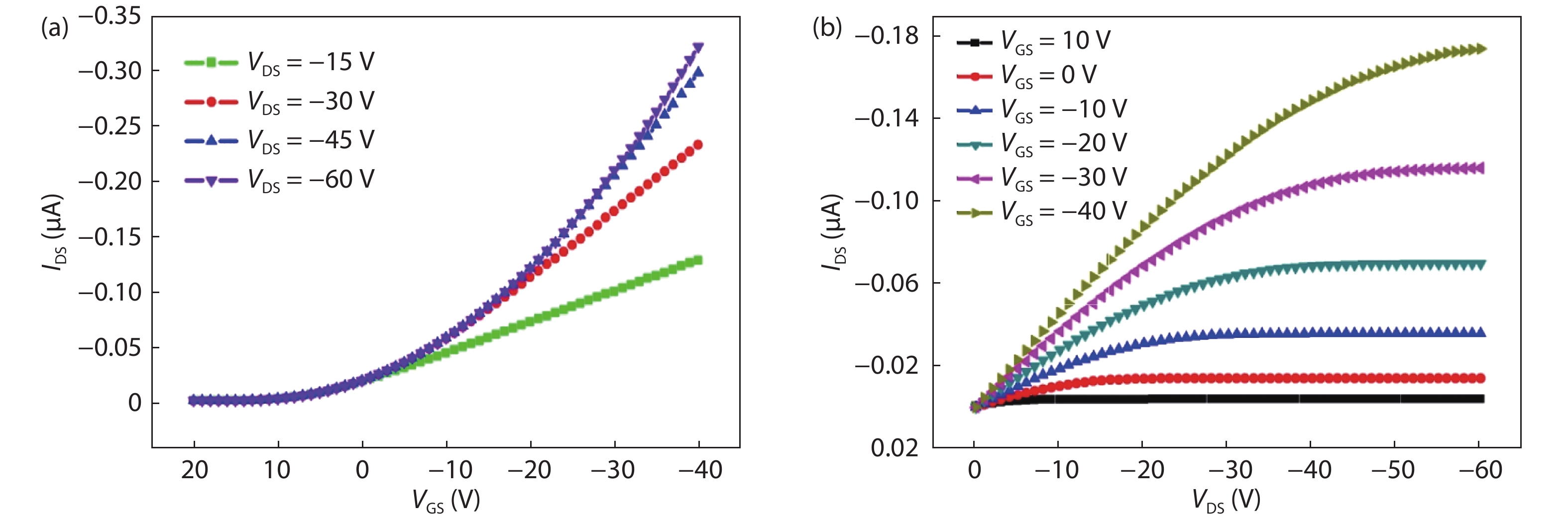
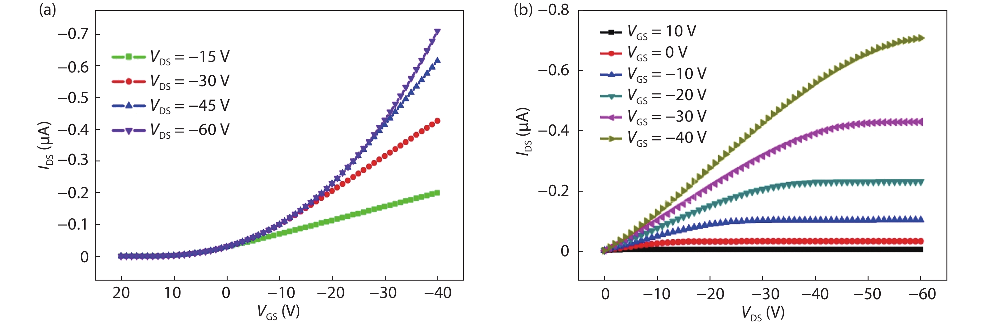
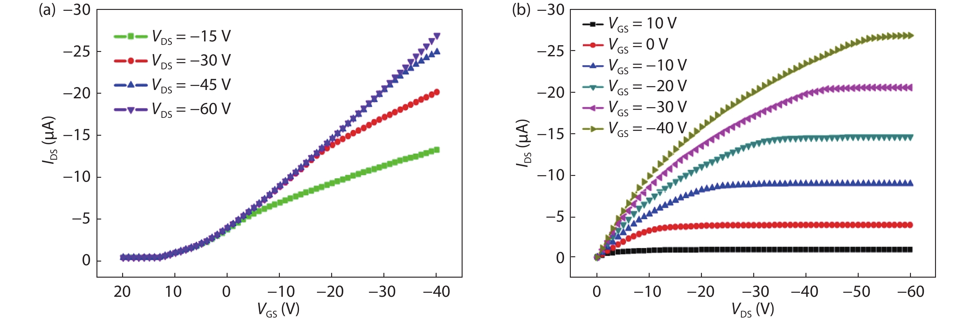
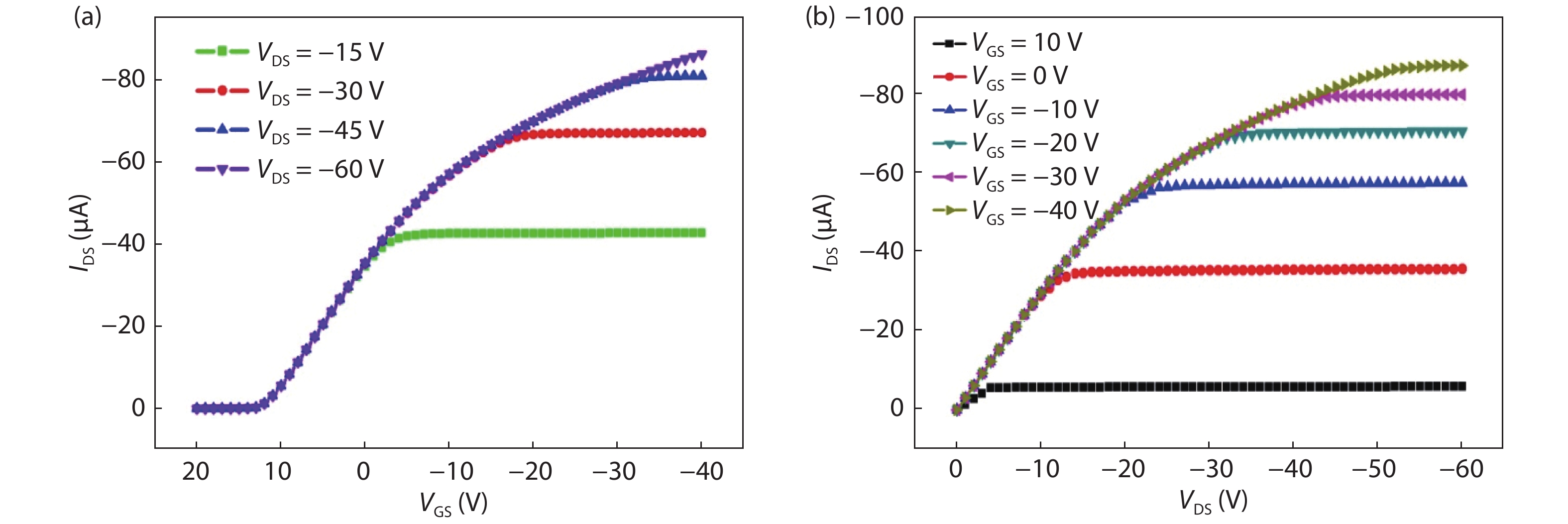
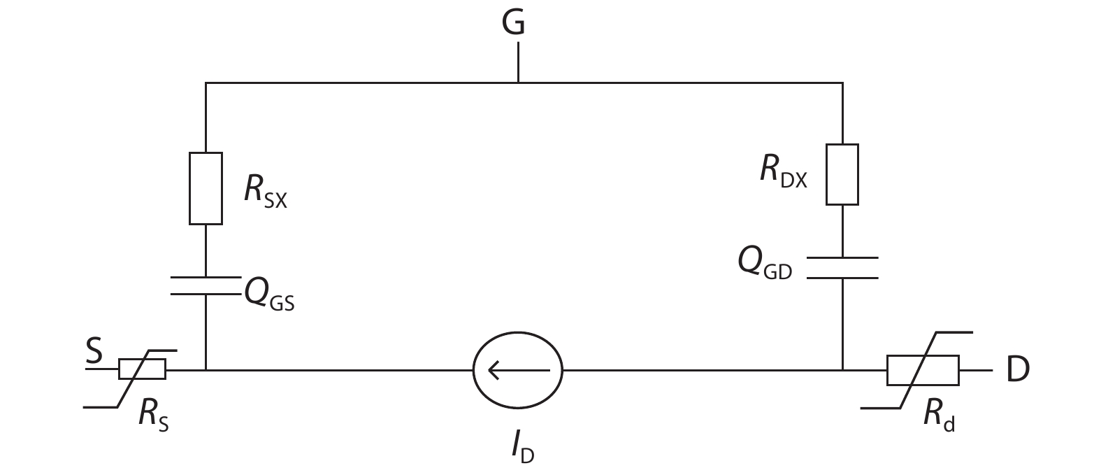
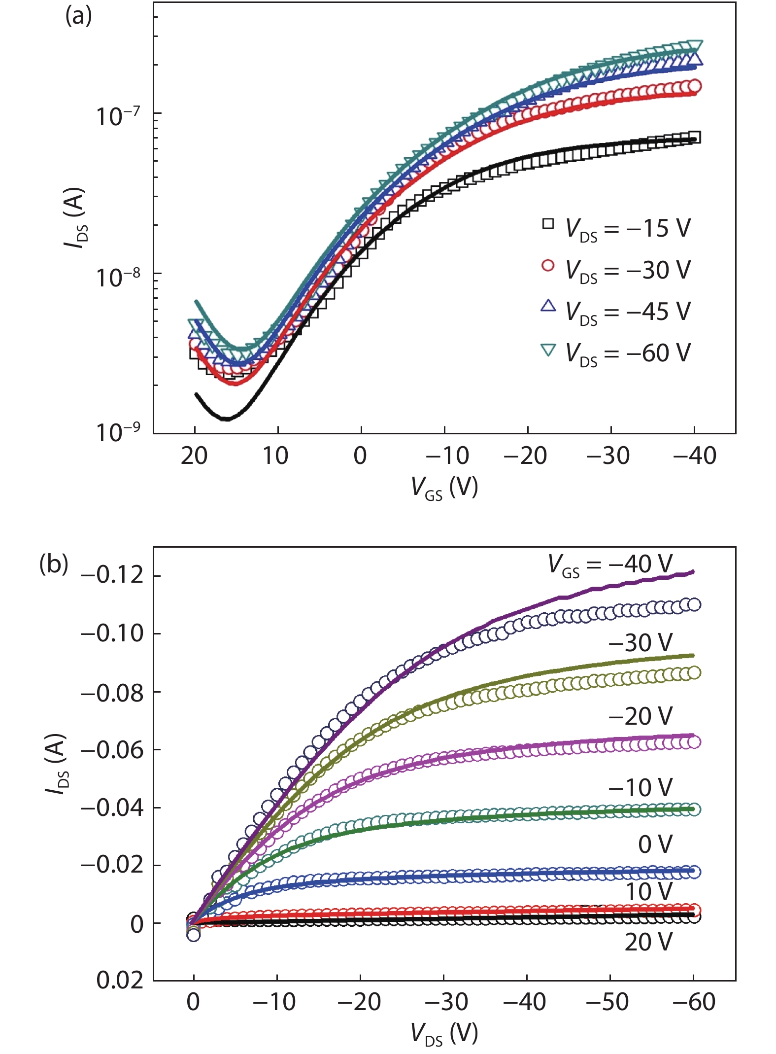
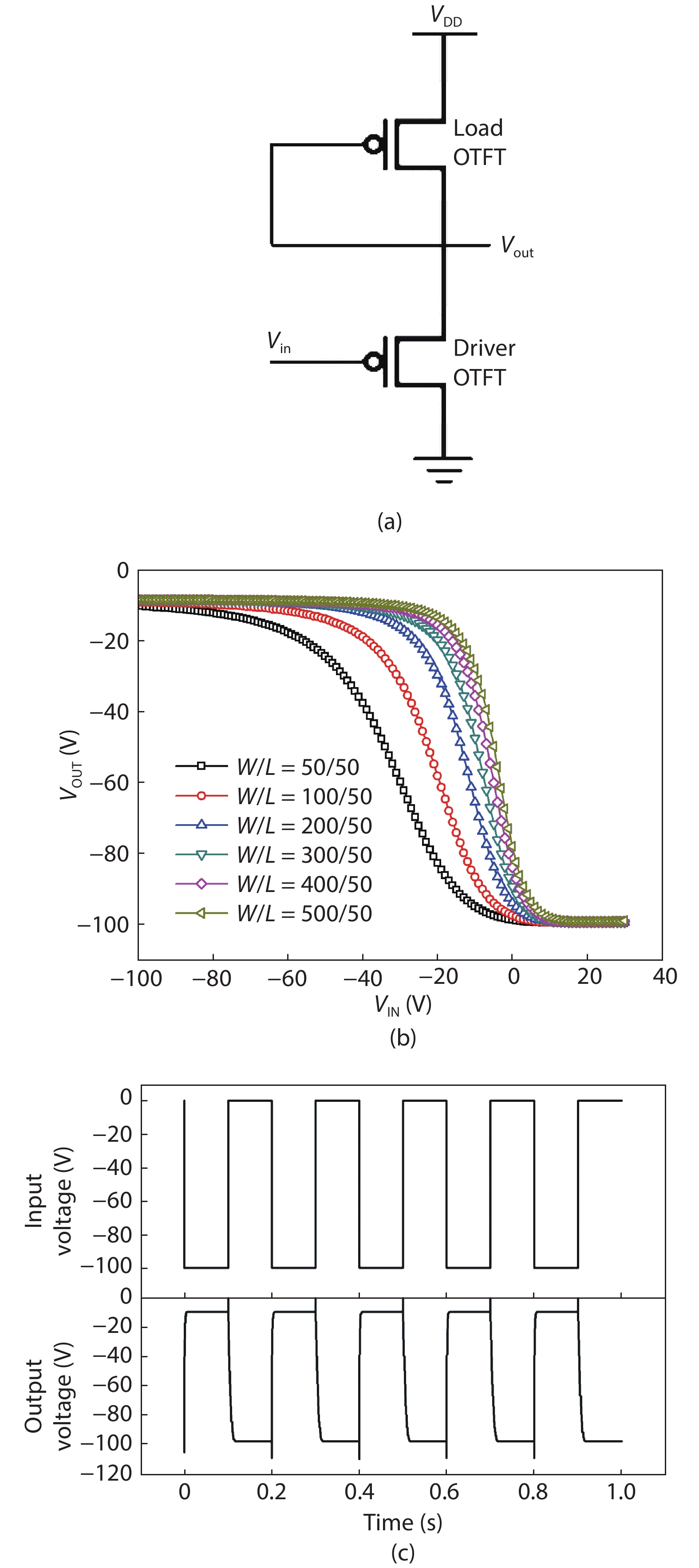
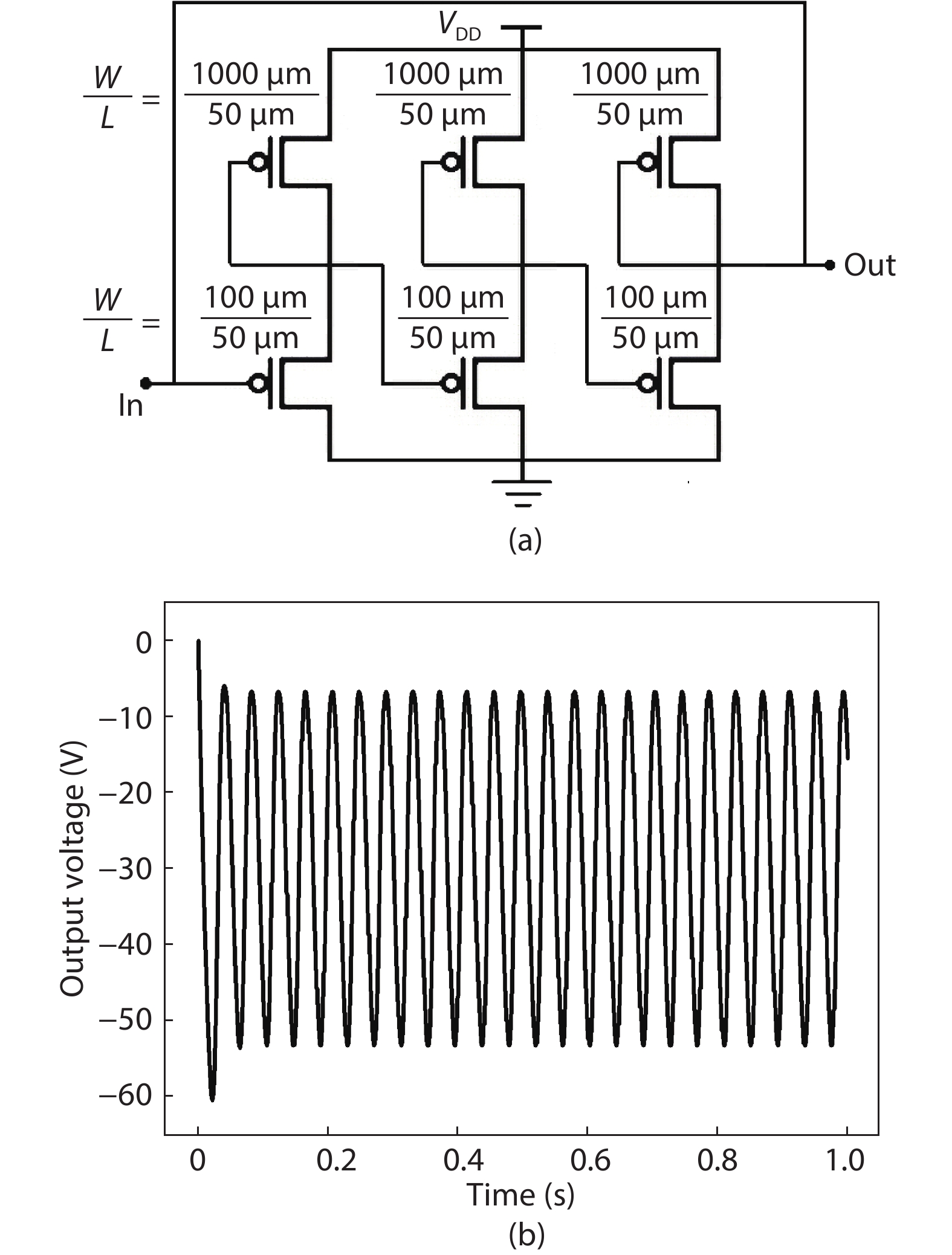
This paper presents the fabrication, characterization and numerical simulation of poly-3-hexylthiophene (P3HT)-based bottom-gate bottom-contact (BGBC) organic thin film transistors (OTFTs). The simulation is based on a drift diffusion charge transport model and density of defect states (DOS) for the traps in the band gap of the P3HT based channel. It combines two mobility models, a hopping mobility model and the Poole–Frenkel mobility model. It also describes the defect density of states (DOS) for both tail and deep states. The model takes into account all the operating regions of the OTFT and includes sub-threshold and above threshold characteristics of OTFTs. The model has been verified by comparing the numerically simulated results with the experimental results. This model is also used to simulate different structure in four configurations of OTFT e.g. bottom-gate bottom-contact (BGBC), bottom-gate top-contact (BGTC), top-gate bottom-contact (TGBC) and top-gate top-contact (TGTC) configurations of the OTFTs. We also present the compact modeling and model parameter extraction of the P3HT-based OTFTs. The extracted compact model has been further applied in a p-channel OTFT-based inverter and three stage ring oscillator circuit simulation.