Issue Browser
Volume 42, Issue 1,
Jan 2021


J. Semicond.
2021, 42(1): 013101 doi: 10.1088/1674-4926/42/1/013101

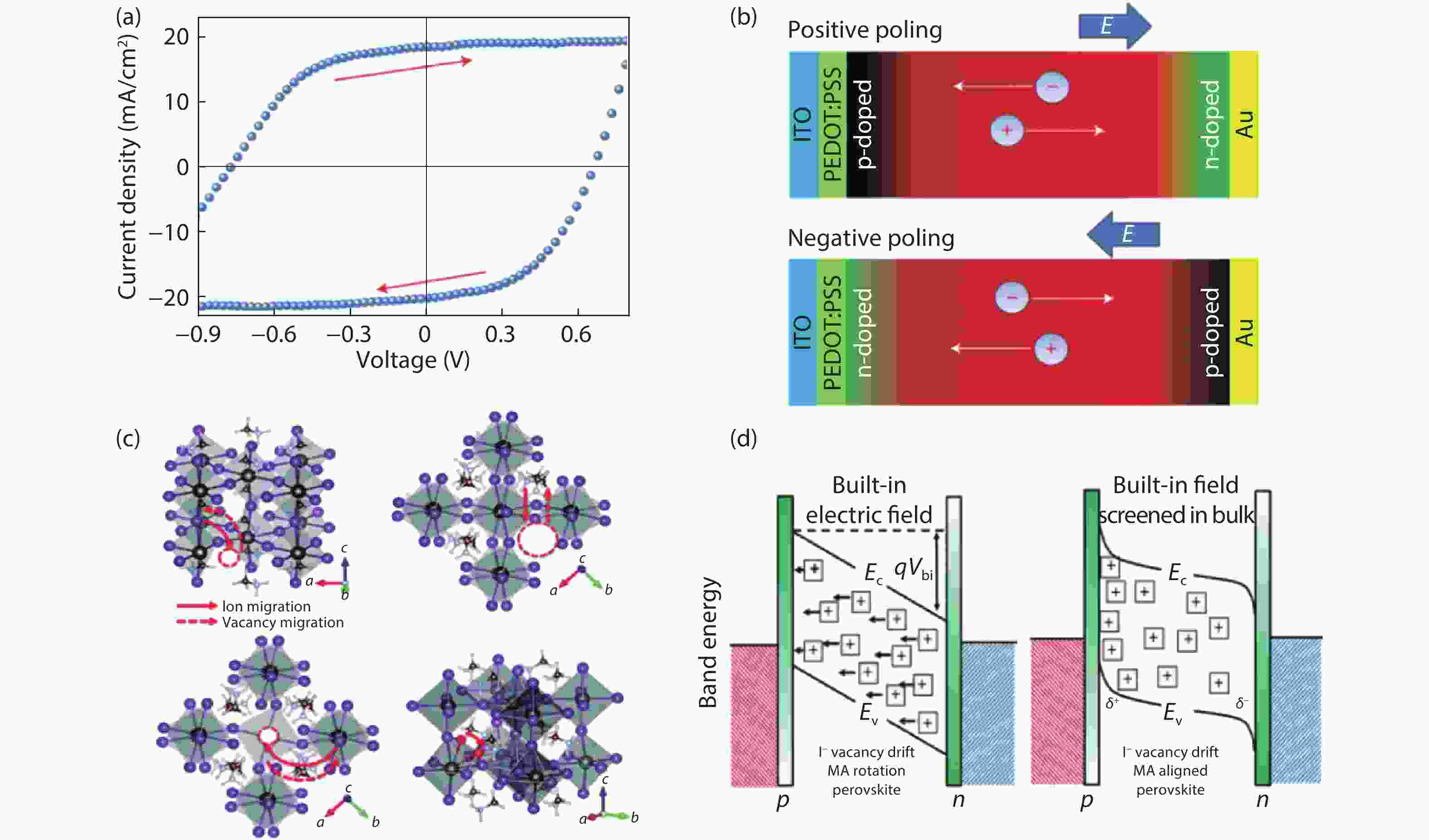
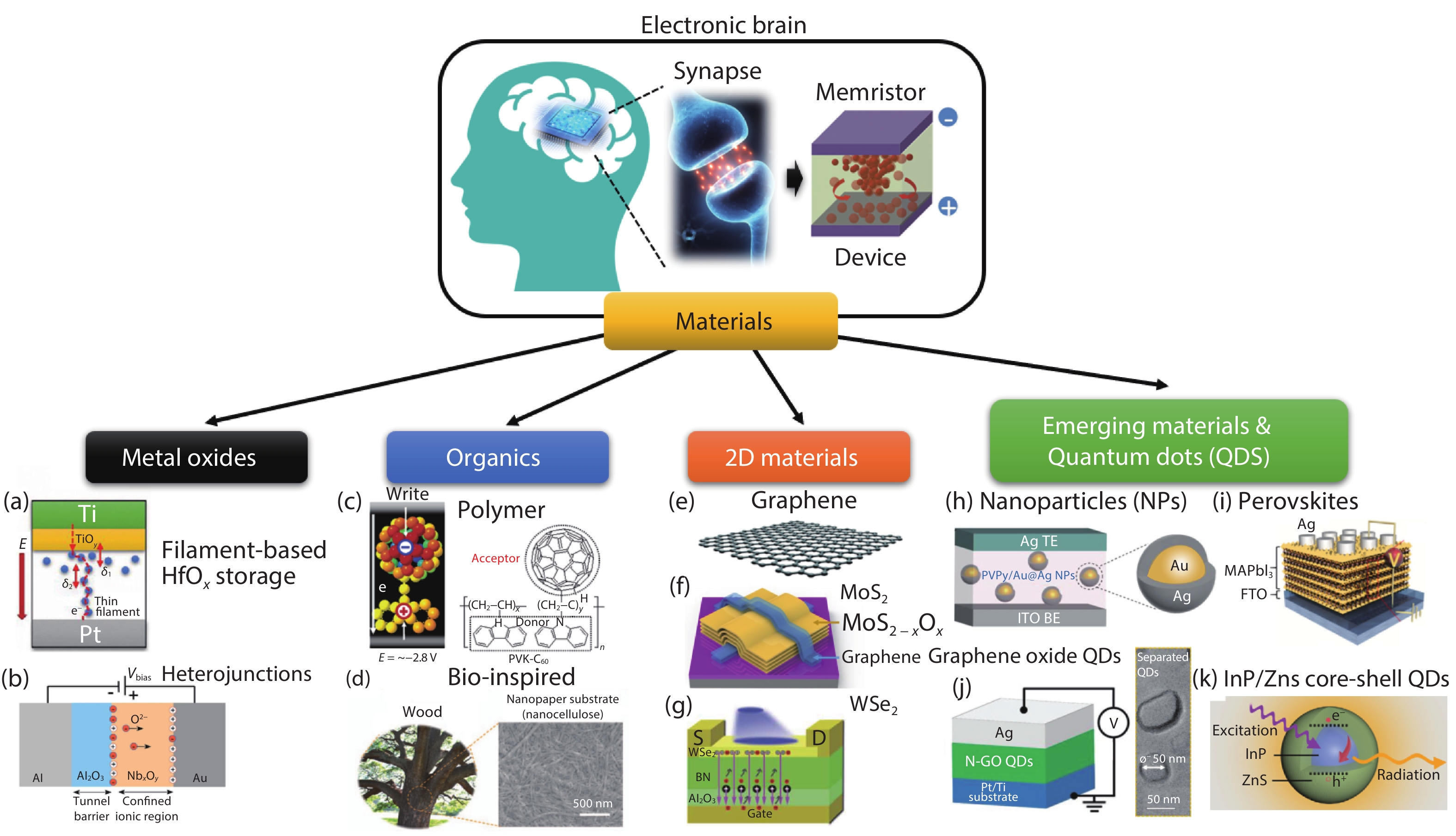
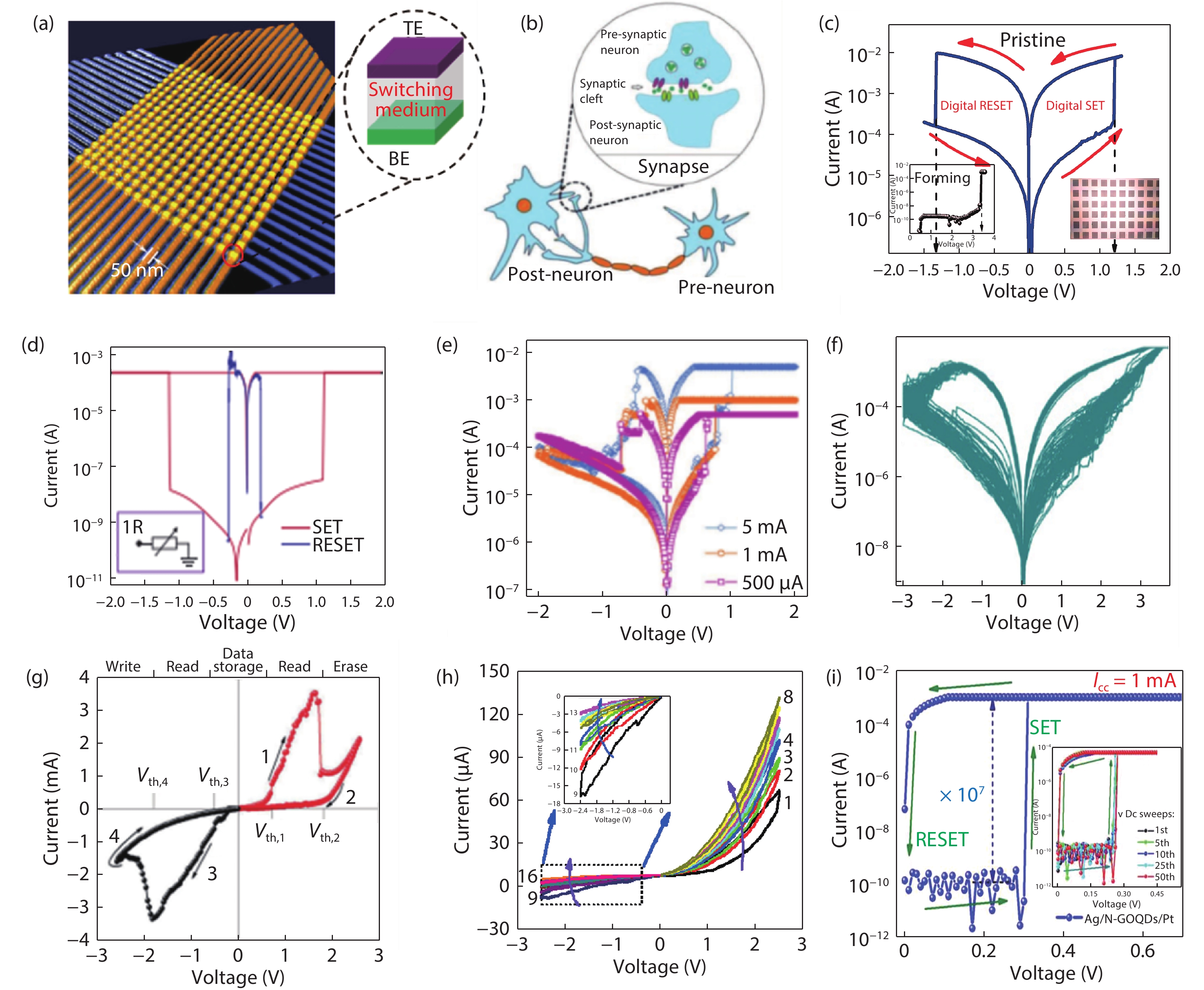
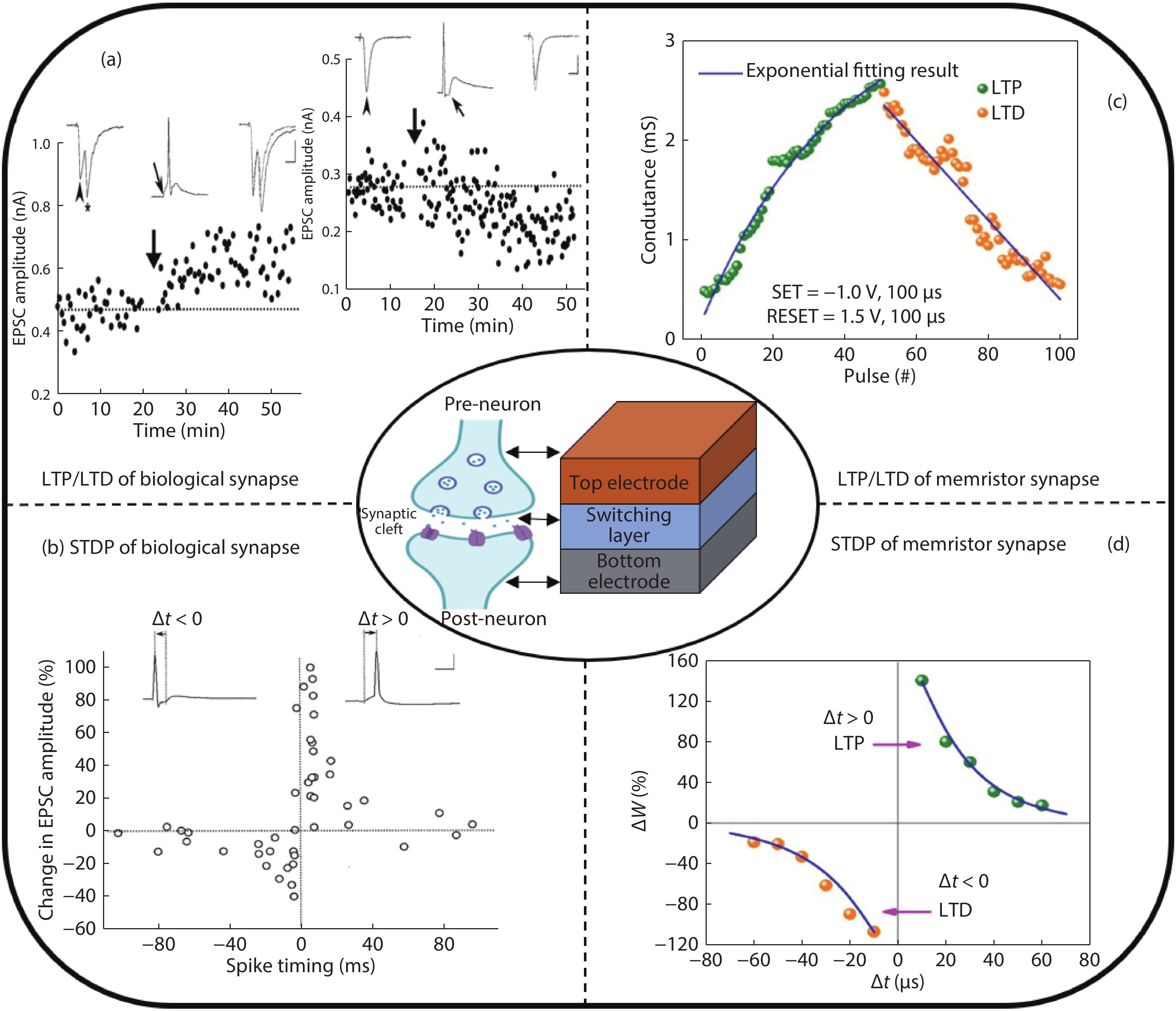
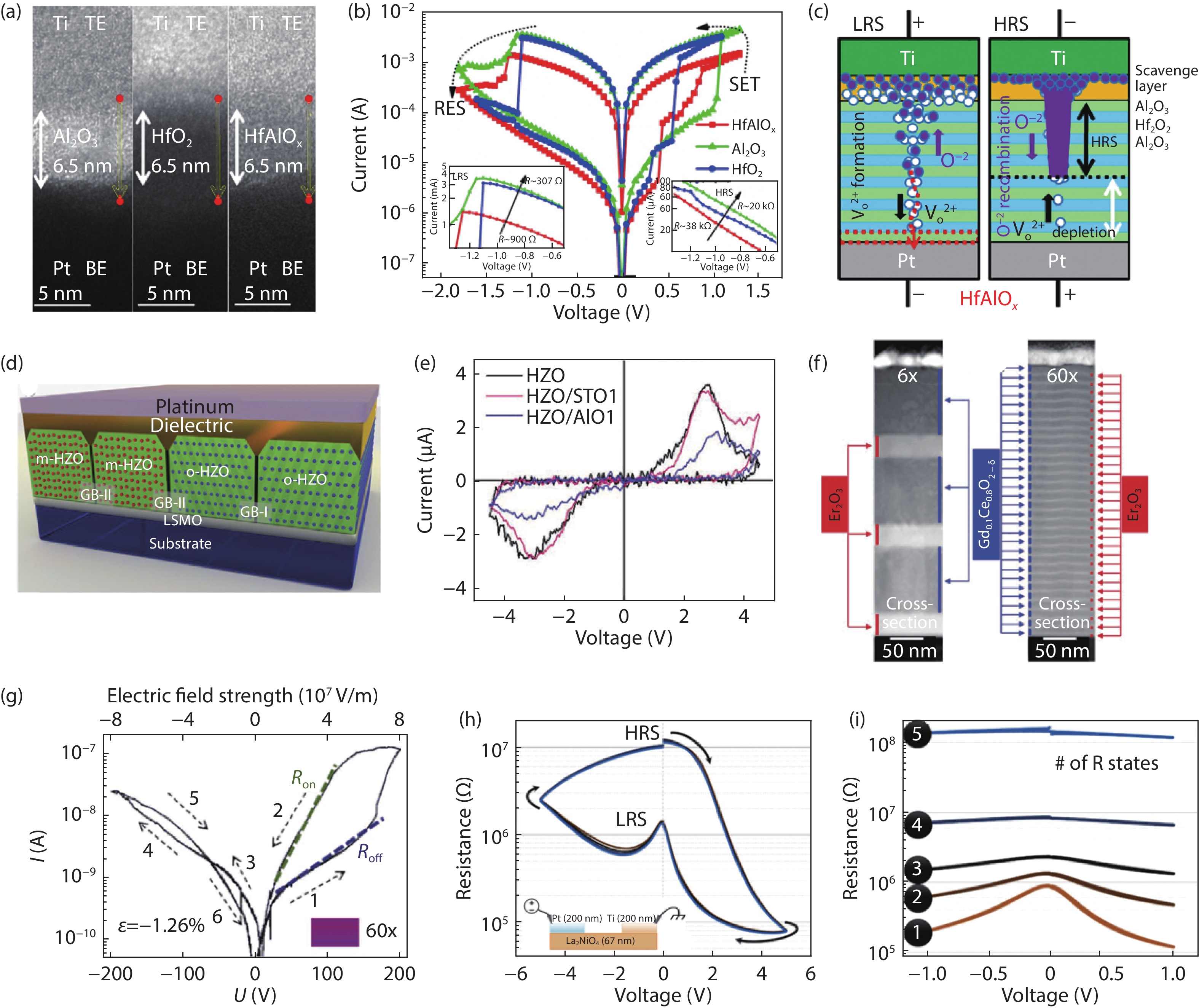
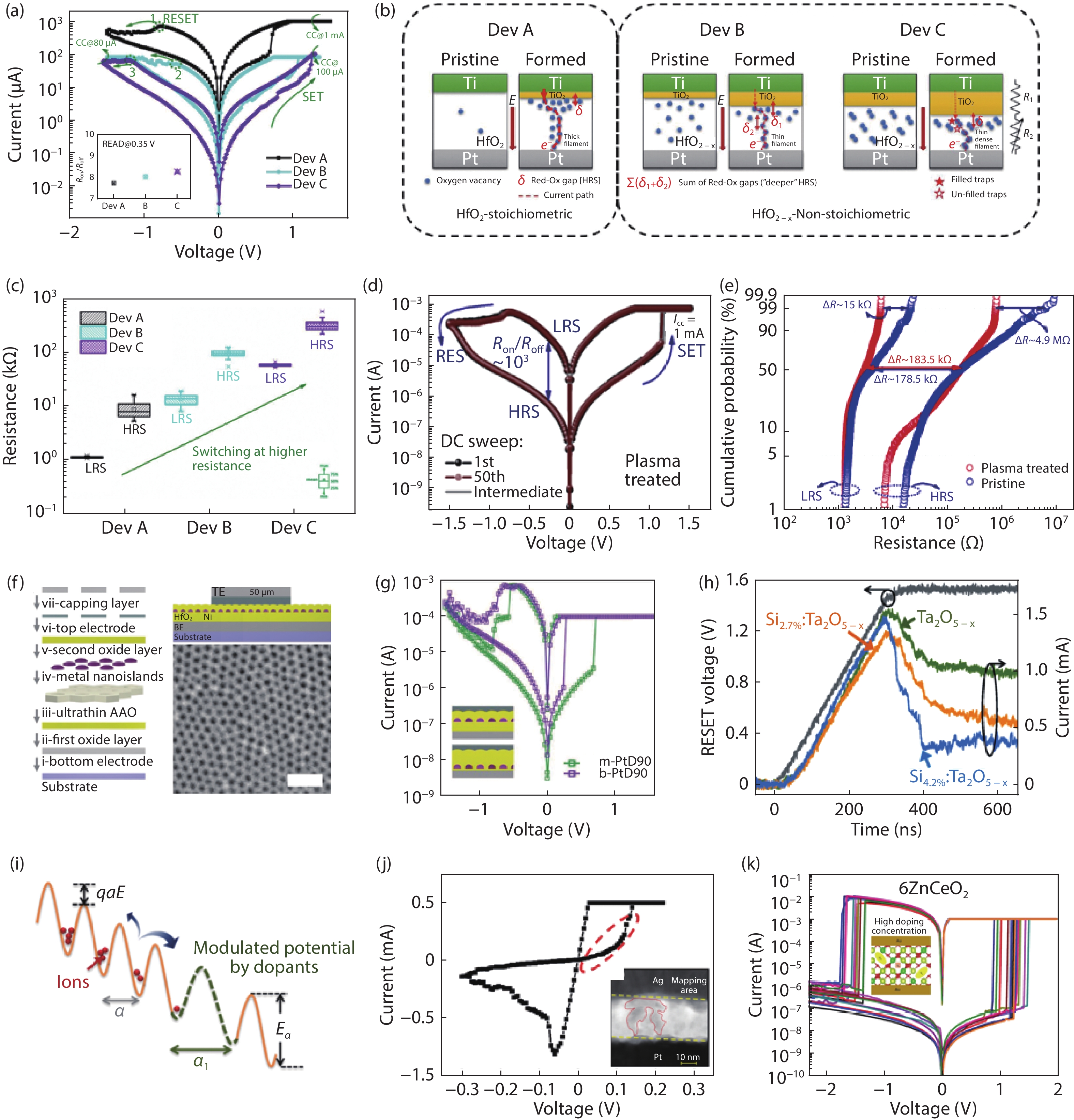
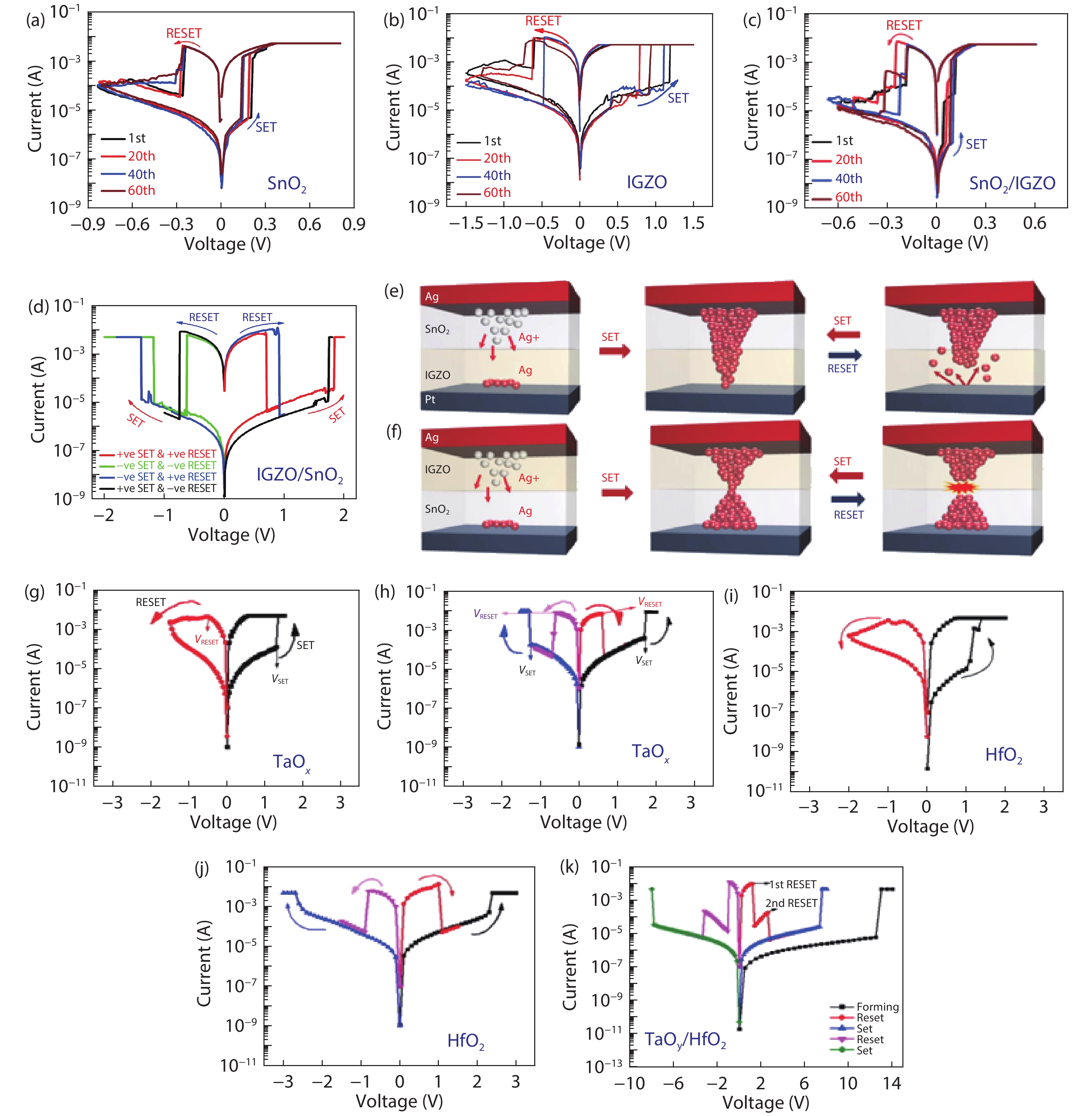
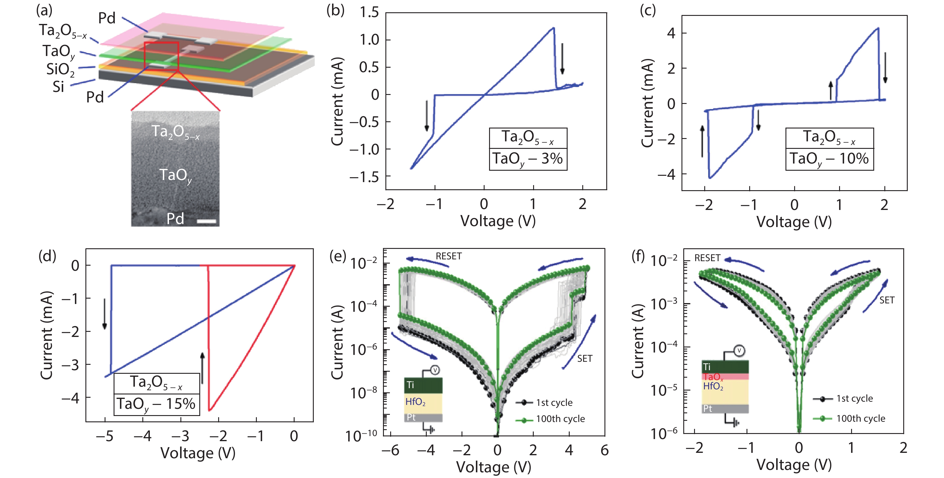
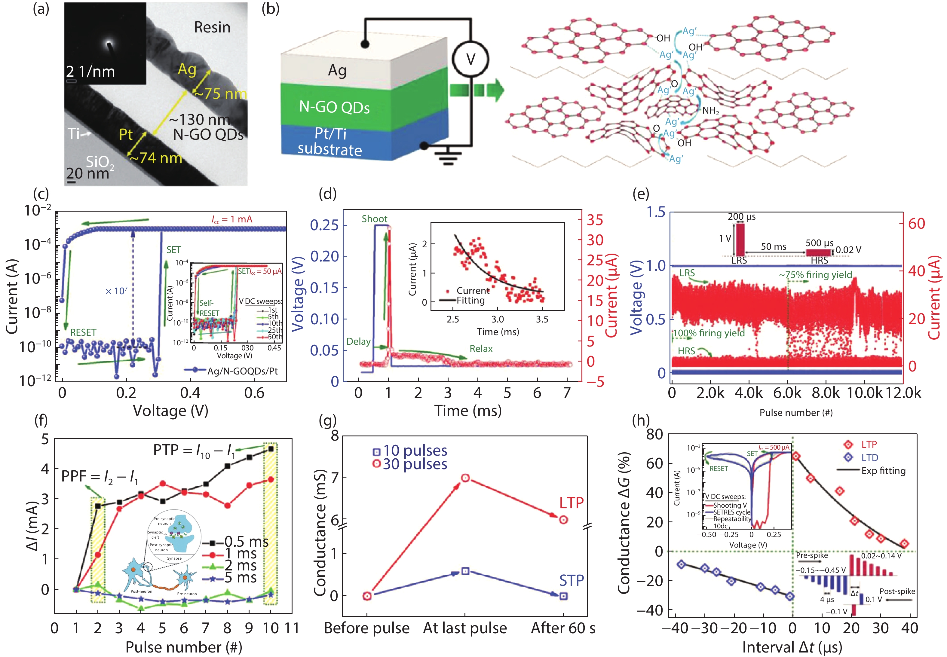
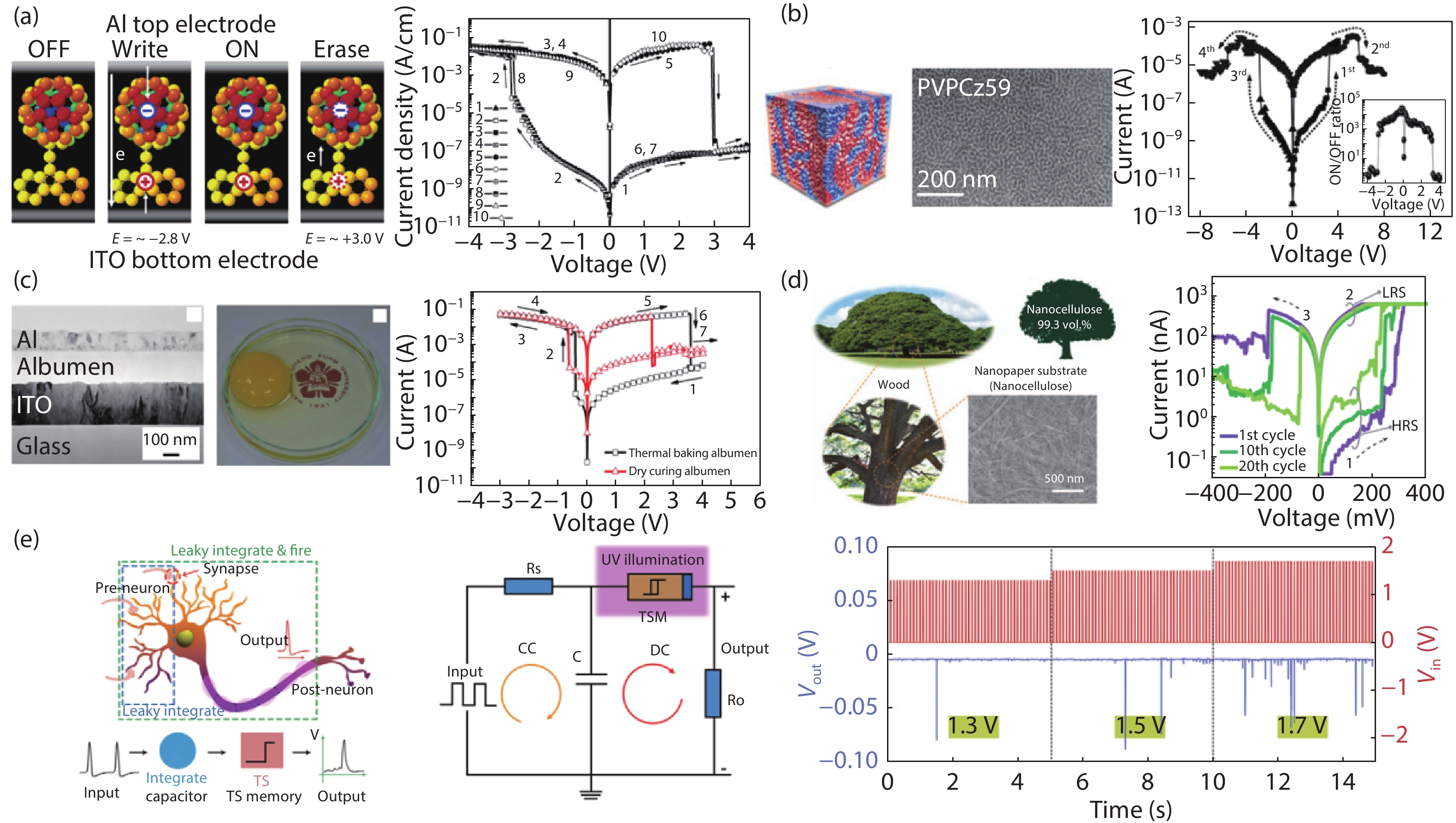
Resistive random-access memory (RRAM), also known as memristors, having a very simple device structure with two terminals, fulfill almost all of the fundamental requirements of volatile memory, nonvolatile memory, and neuromorphic characteristics. Its memory and neuromorphic behaviors are currently being explored in relation to a range of materials, such as biological materials, perovskites, 2D materials, and transition metal oxides. In this review, we discuss the different electrical behaviors exhibited by RRAM devices based on these materials by briefly explaining their corresponding switching mechanisms. We then discuss emergent memory technologies using memristors, together with its potential neuromorphic applications, by elucidating the different material engineering techniques used during device fabrication to improve the memory and neuromorphic performance of devices, in areas such as ION/IOFF ratio, endurance, spike time-dependent plasticity (STDP), and paired-pulse facilitation (PPF), among others. The emulation of essential biological synaptic functions realized in various switching materials, including inorganic metal oxides and new organic materials, as well as diverse device structures such as single-layer and multilayer hetero-structured devices, and crossbar arrays, is analyzed in detail. Finally, we discuss current challenges and future prospects for the development of inorganic and new materials-based memristors.


J. Semicond.
2021, 42(1): 013102 doi: 10.1088/1674-4926/42/1/013102

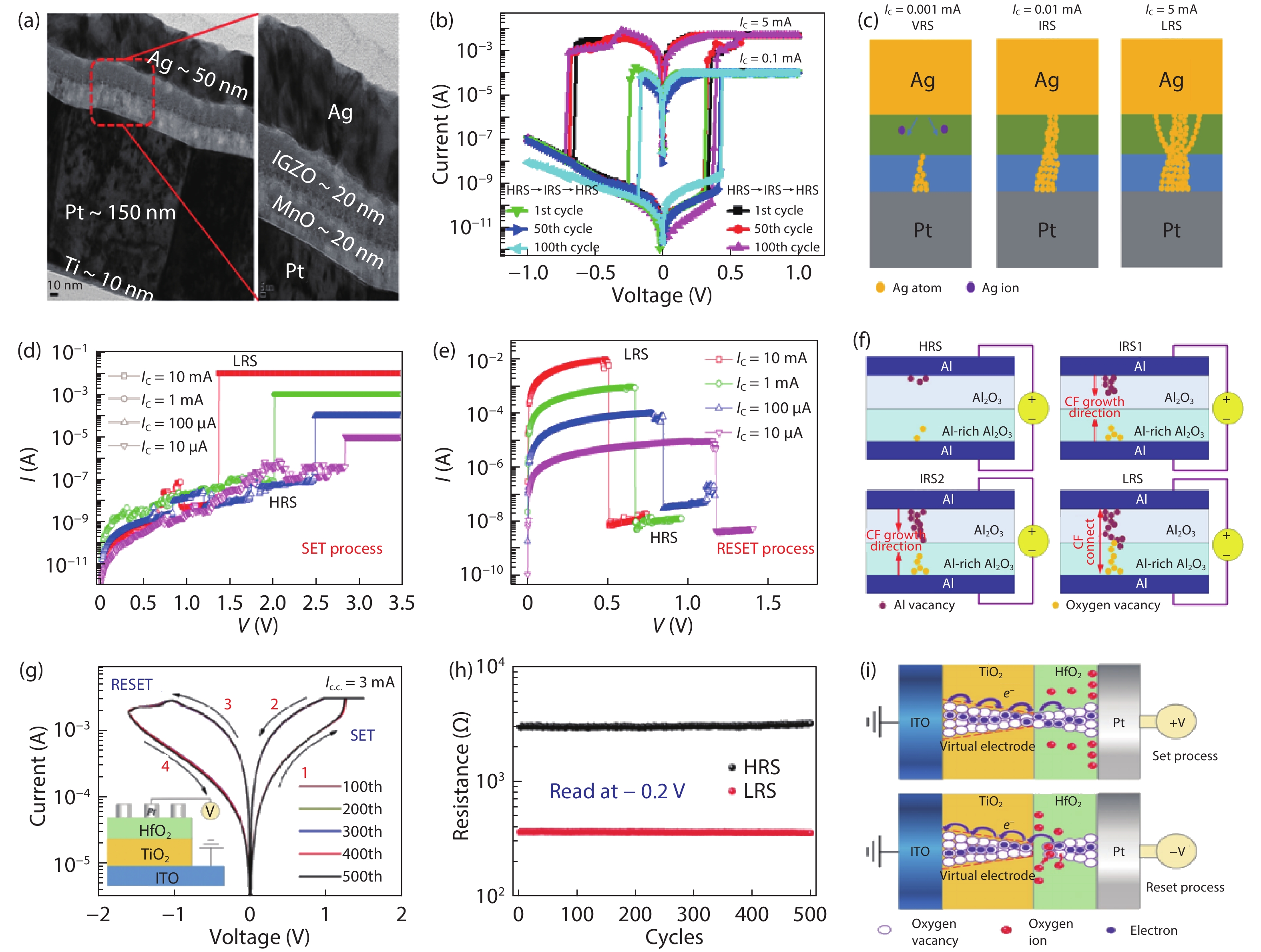
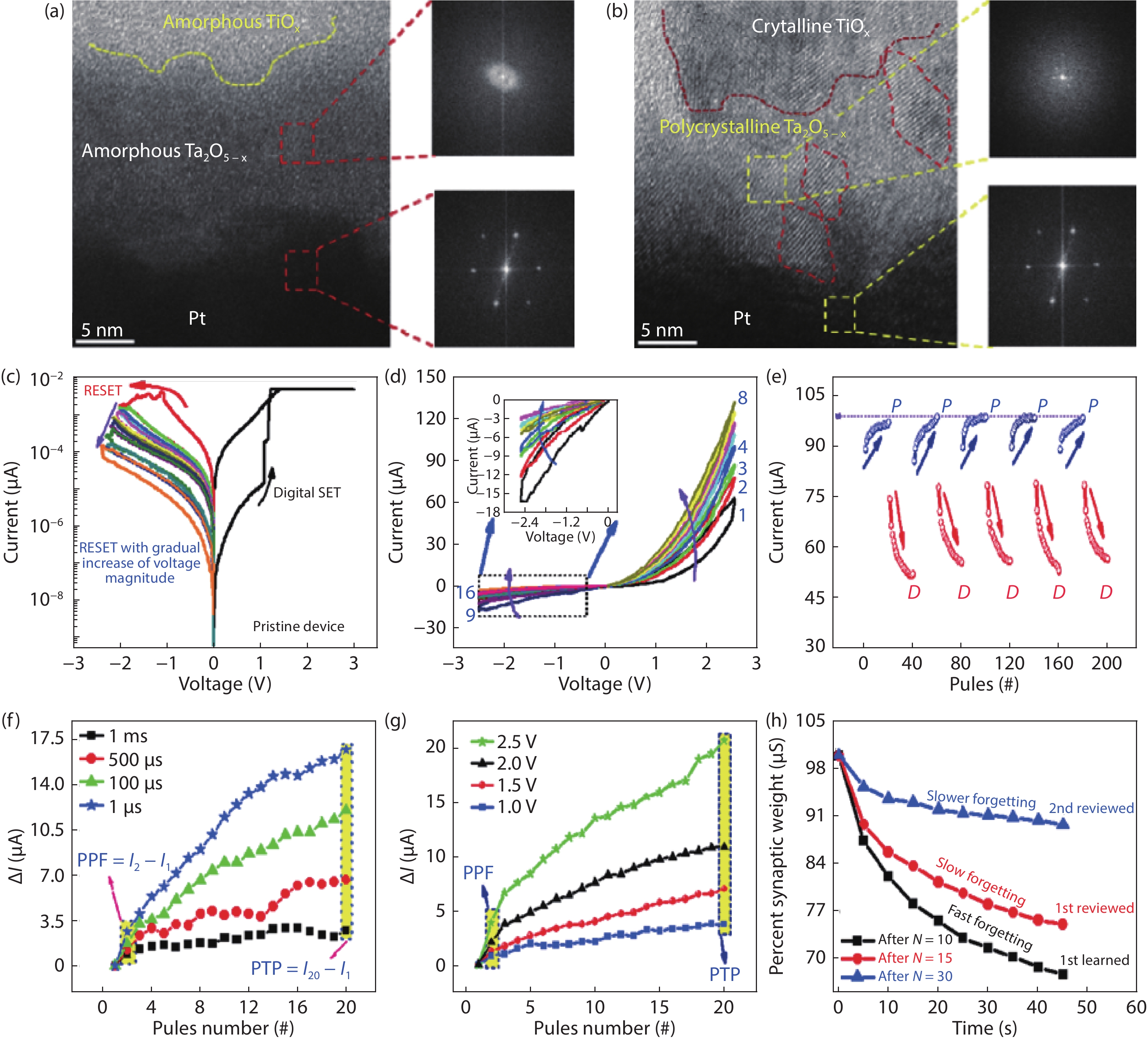
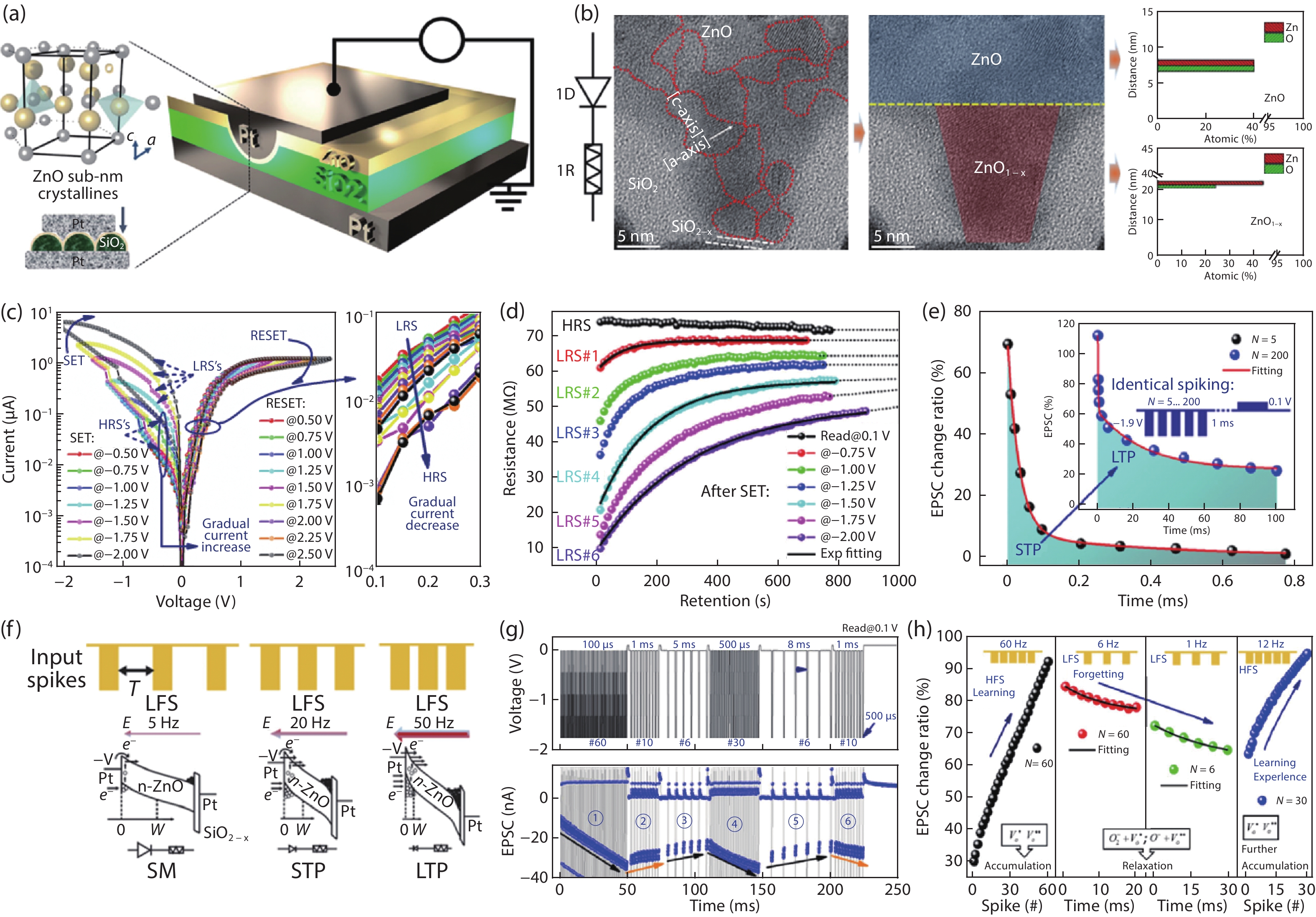
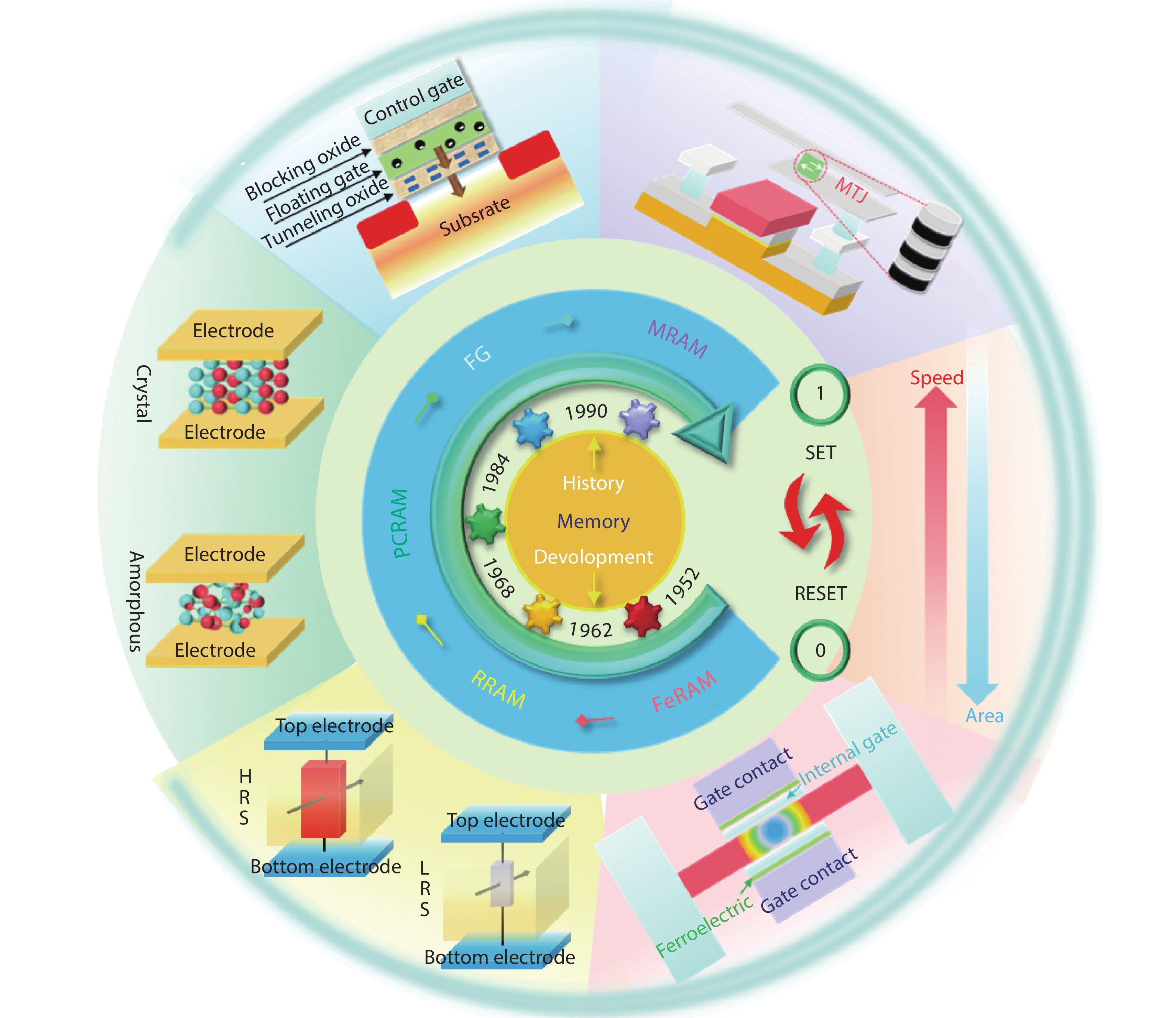
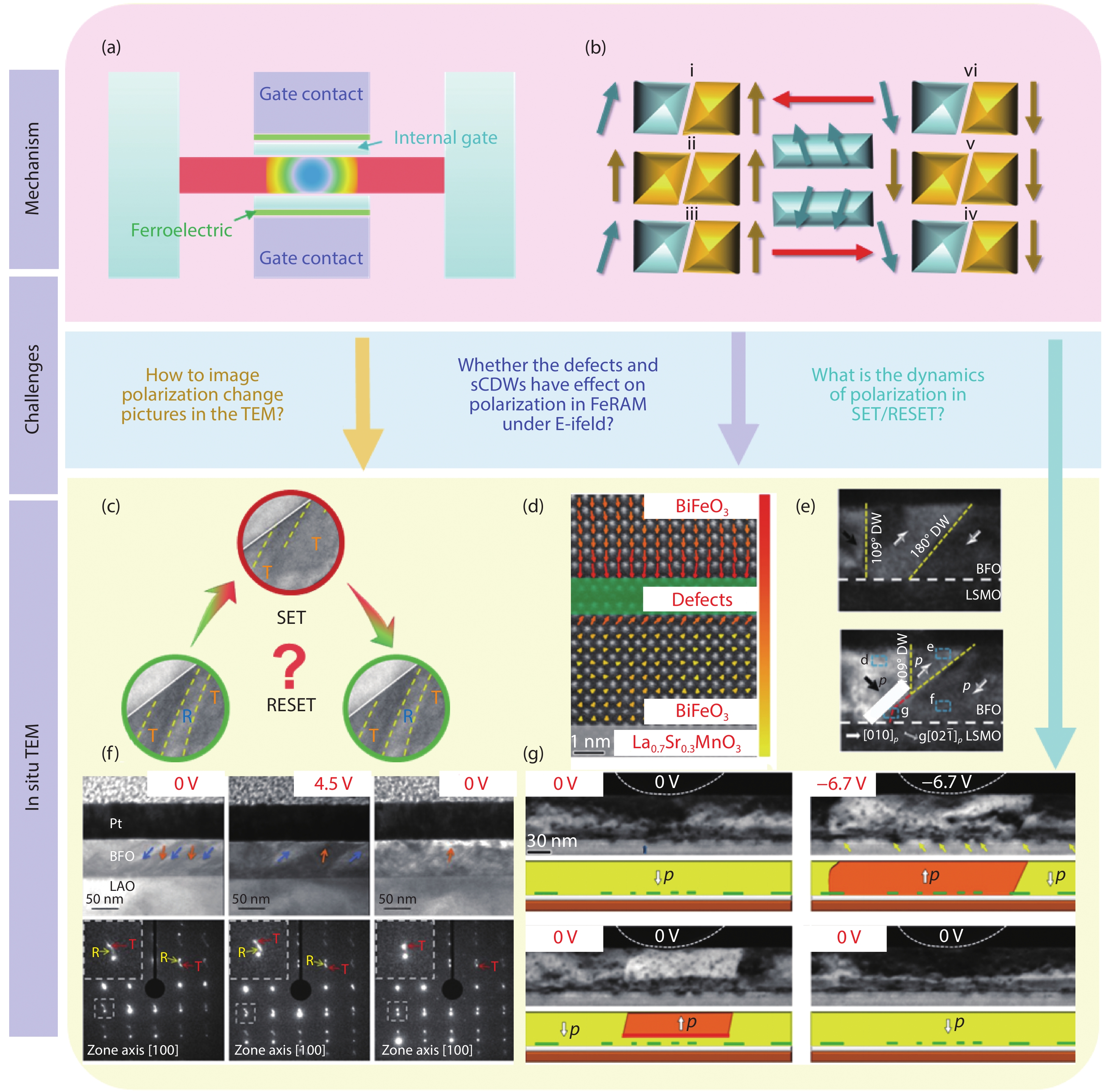
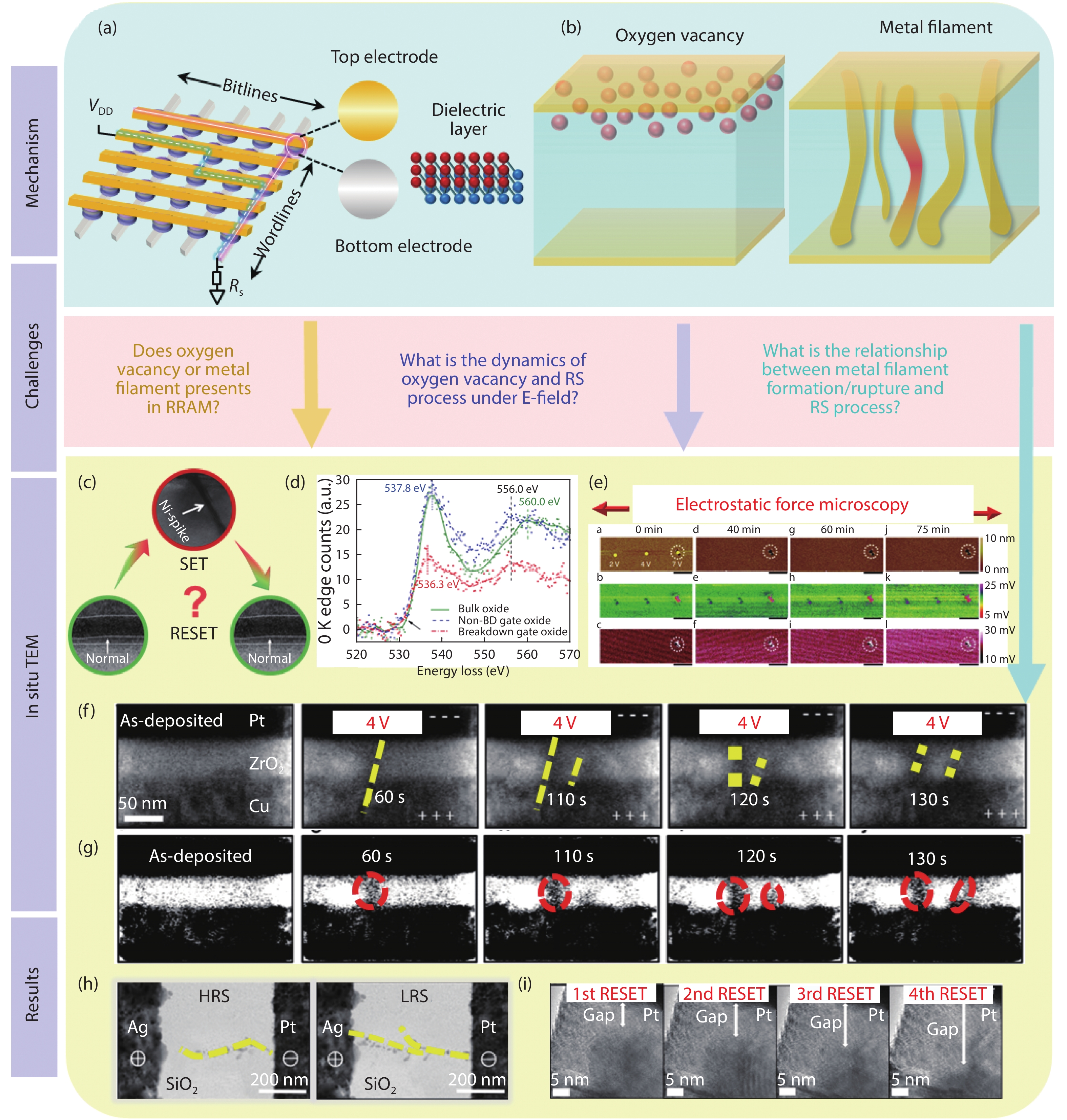
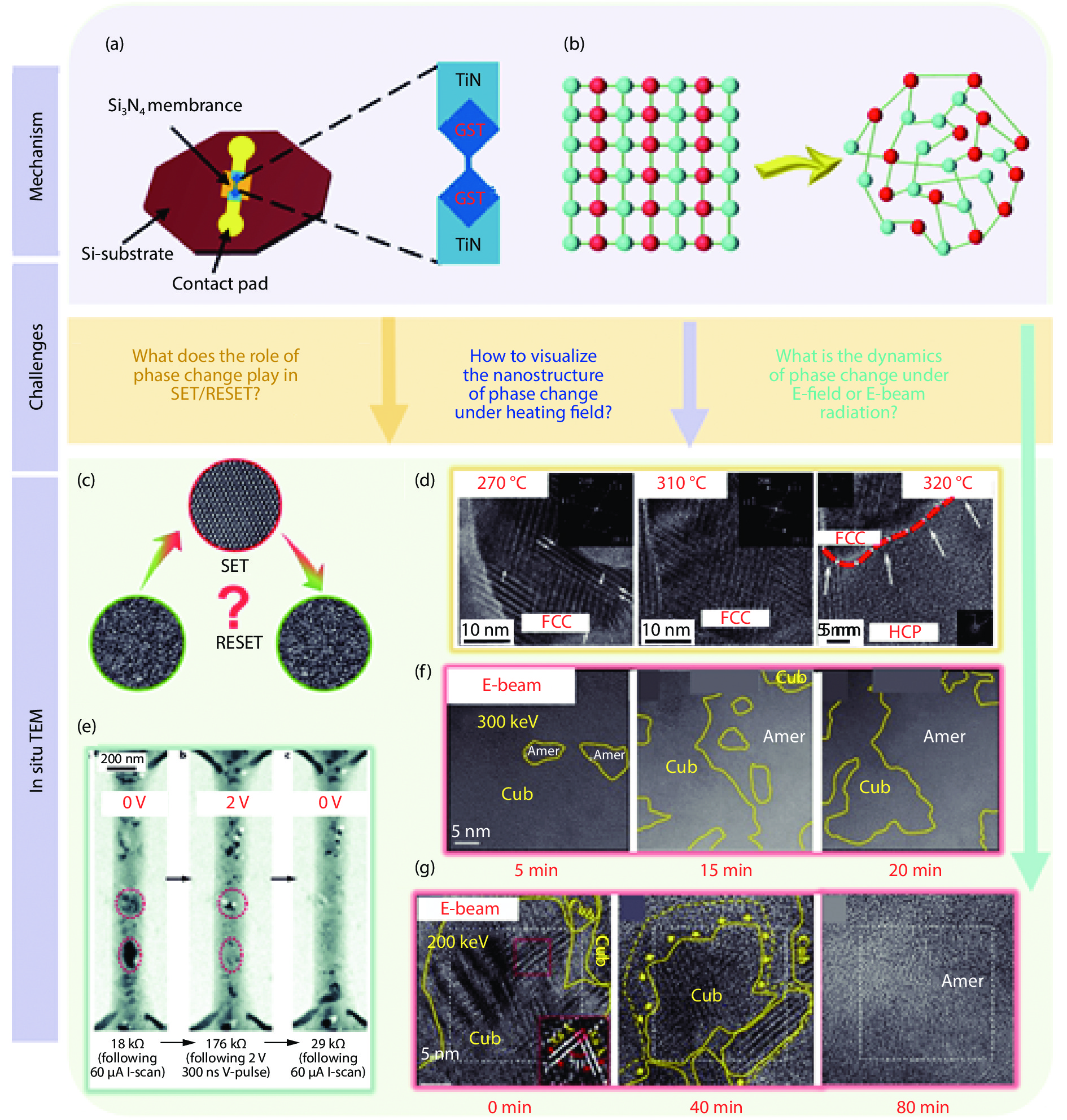
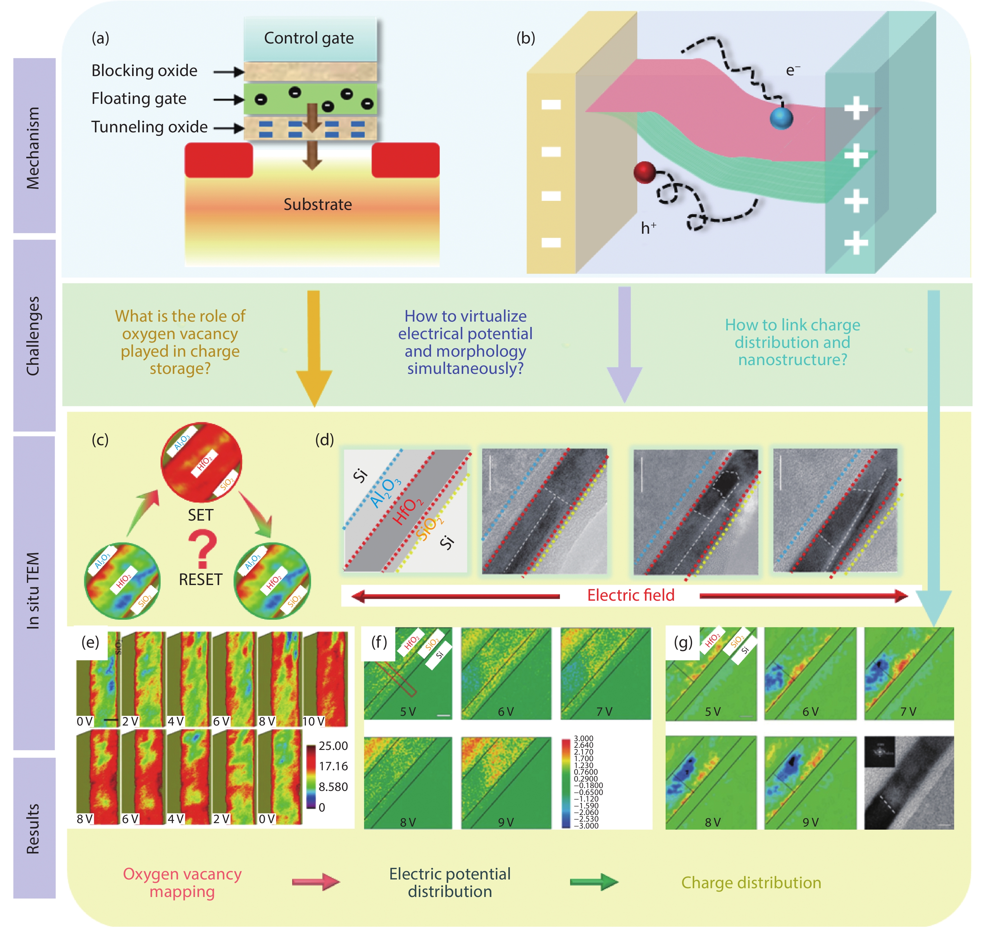
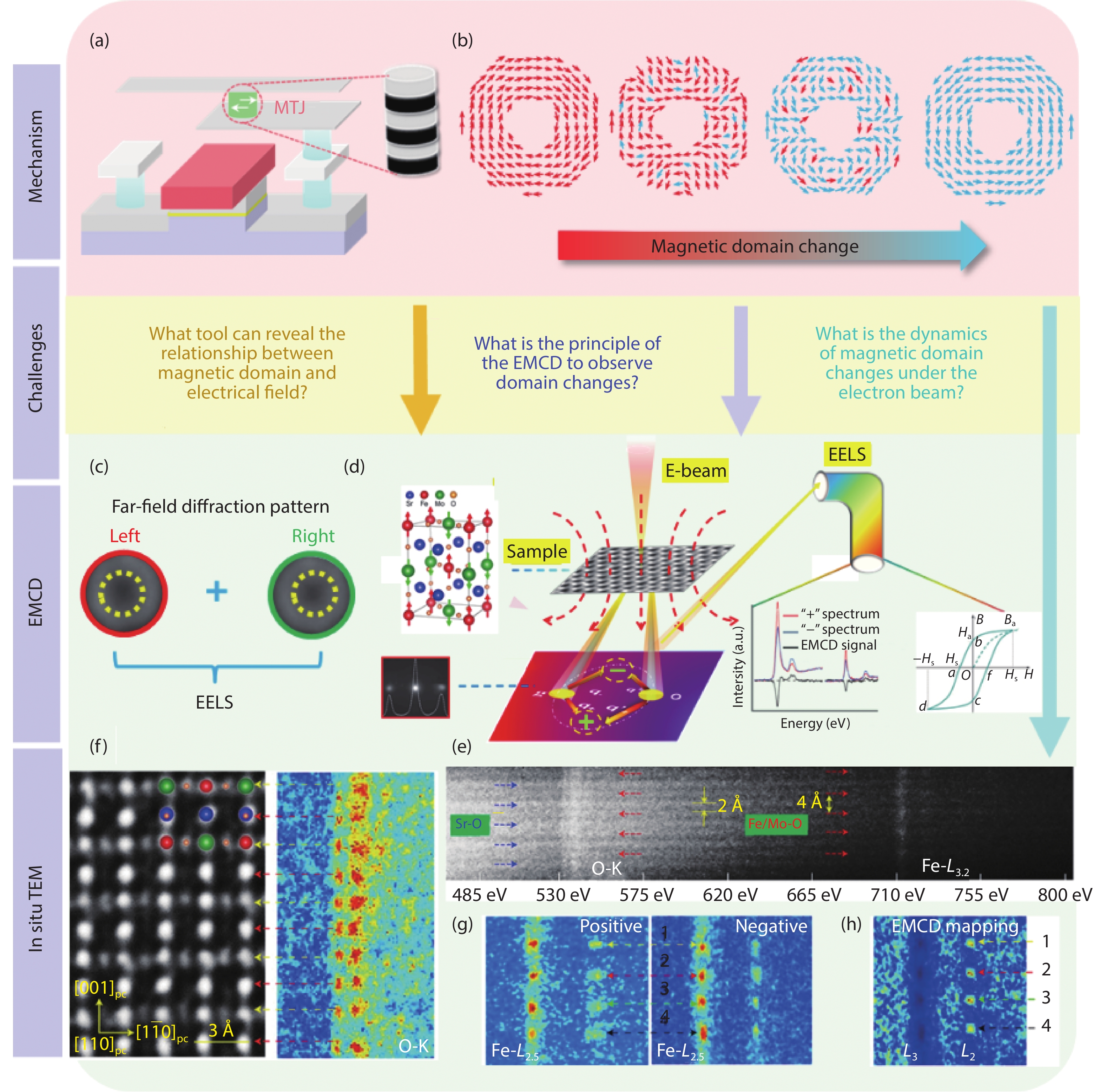
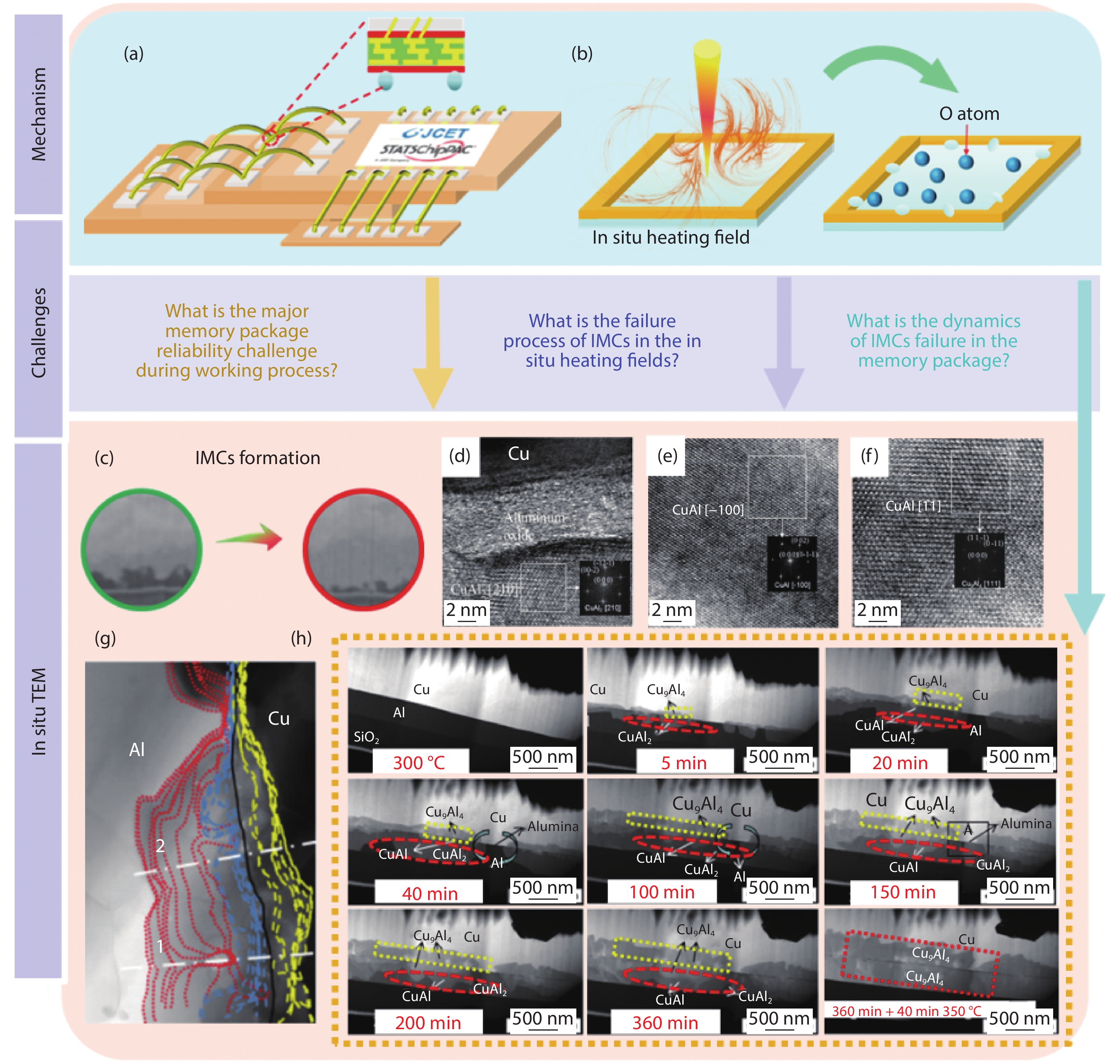
Non-volatile memory (NVM) devices with non-volatility and low power consumption properties are important in the data storage field. The switching mechanism and packaging reliability issues in NVMs are of great research interest. The switching process in NVM devices accompanied by the evolution of microstructure and composition is fast and subtle. Transmission electron microscopy (TEM) with high spatial resolution and versatile external fields is widely used in analyzing the evolution of morphology, structures and chemical compositions at atomic scale. The various external stimuli, such as thermal, electrical, mechanical, optical and magnetic fields, provide a platform to probe and engineer NVM devices inside TEM in real-time. Such advanced technologies make it possible for an in situ and interactive manipulation of NVM devices without sacrificing the resolution. This technology facilitates the exploration of the intrinsic structure-switching mechanism of NVMs and the reliability issues in the memory package. In this review, the evolution of the functional layers in NVM devices characterized by the advanced in situ TEM technology is introduced, with intermetallic compounds forming and degradation process investigated. The principles and challenges of TEM technology on NVM device study are also discussed.

J. Semicond.
2021, 42(1): 013103 doi: 10.1088/1674-4926/42/1/013103
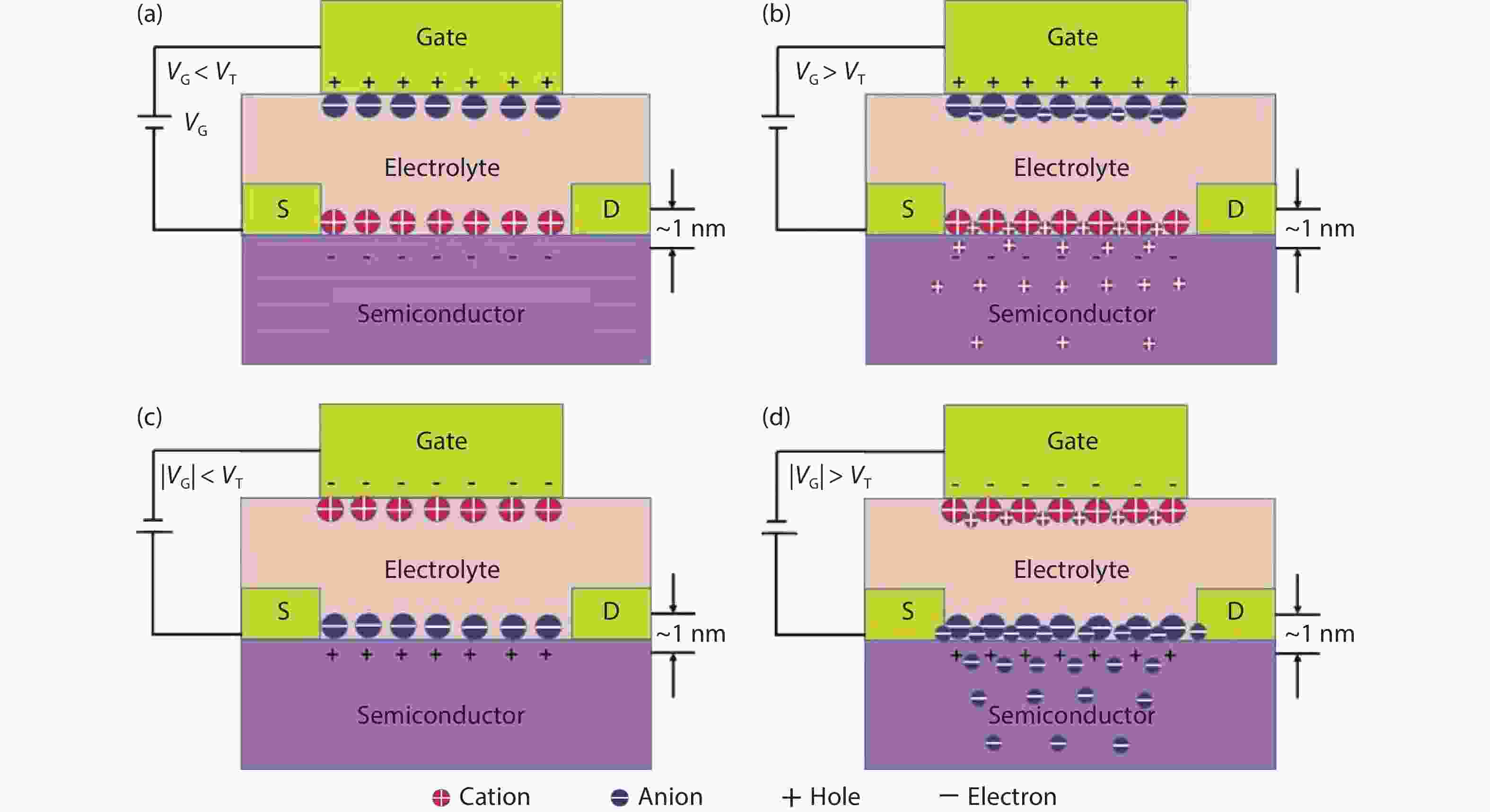
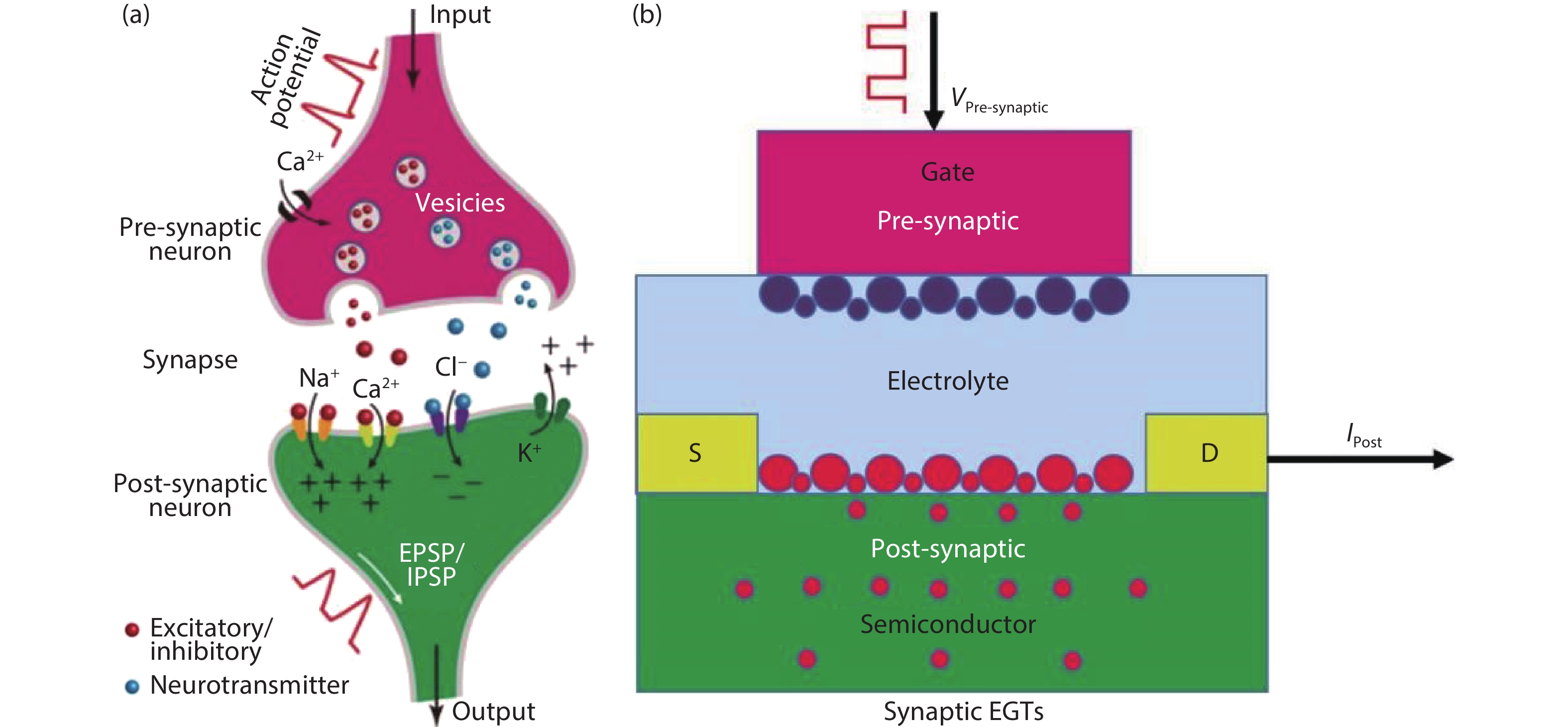
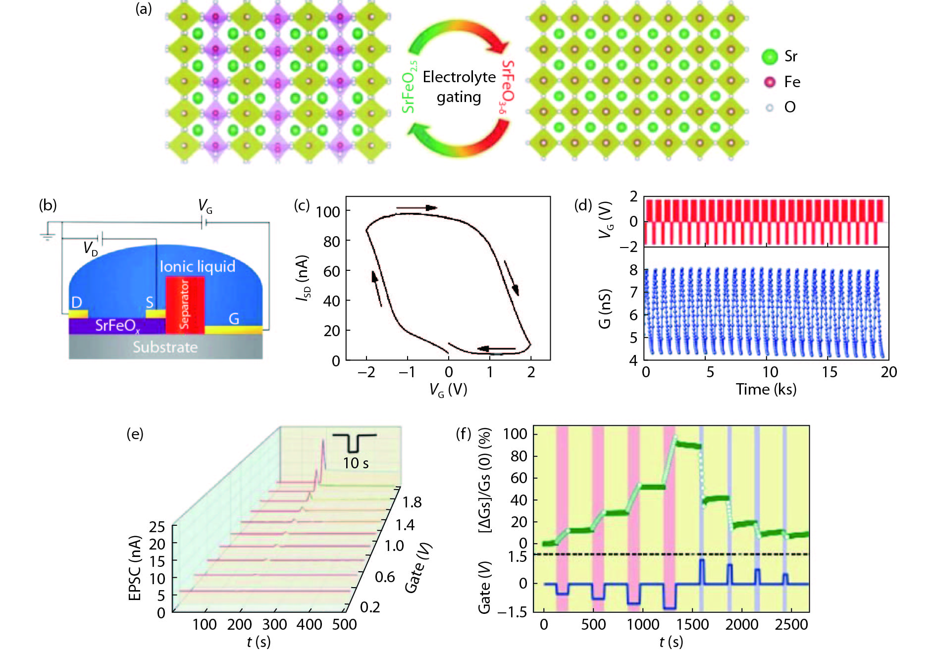
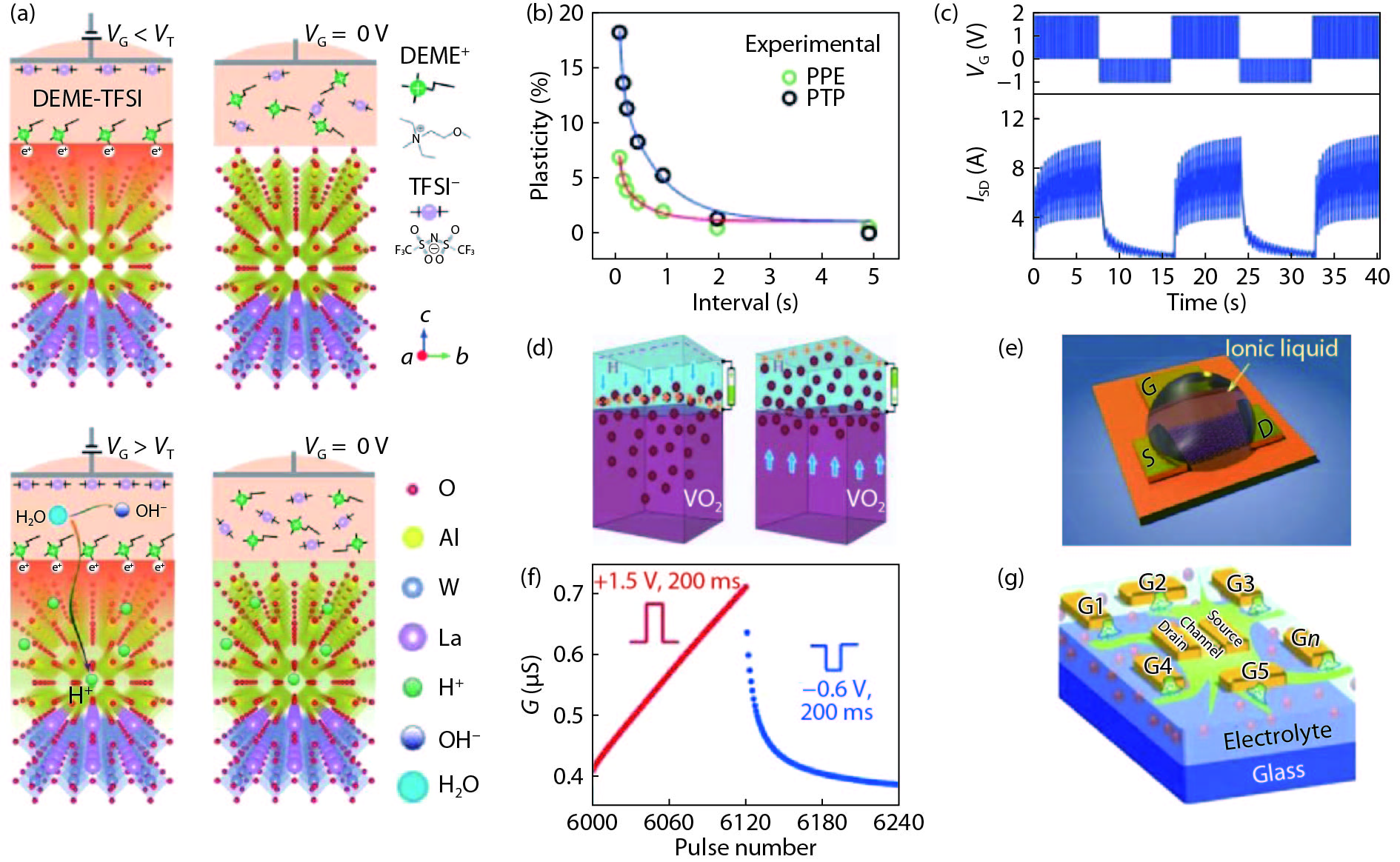
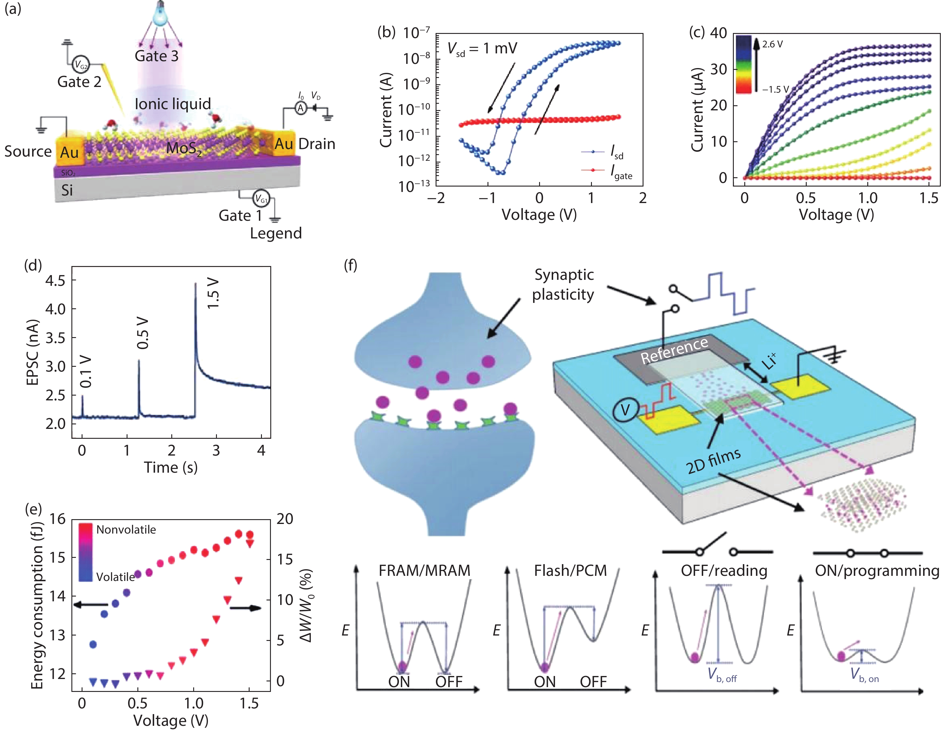
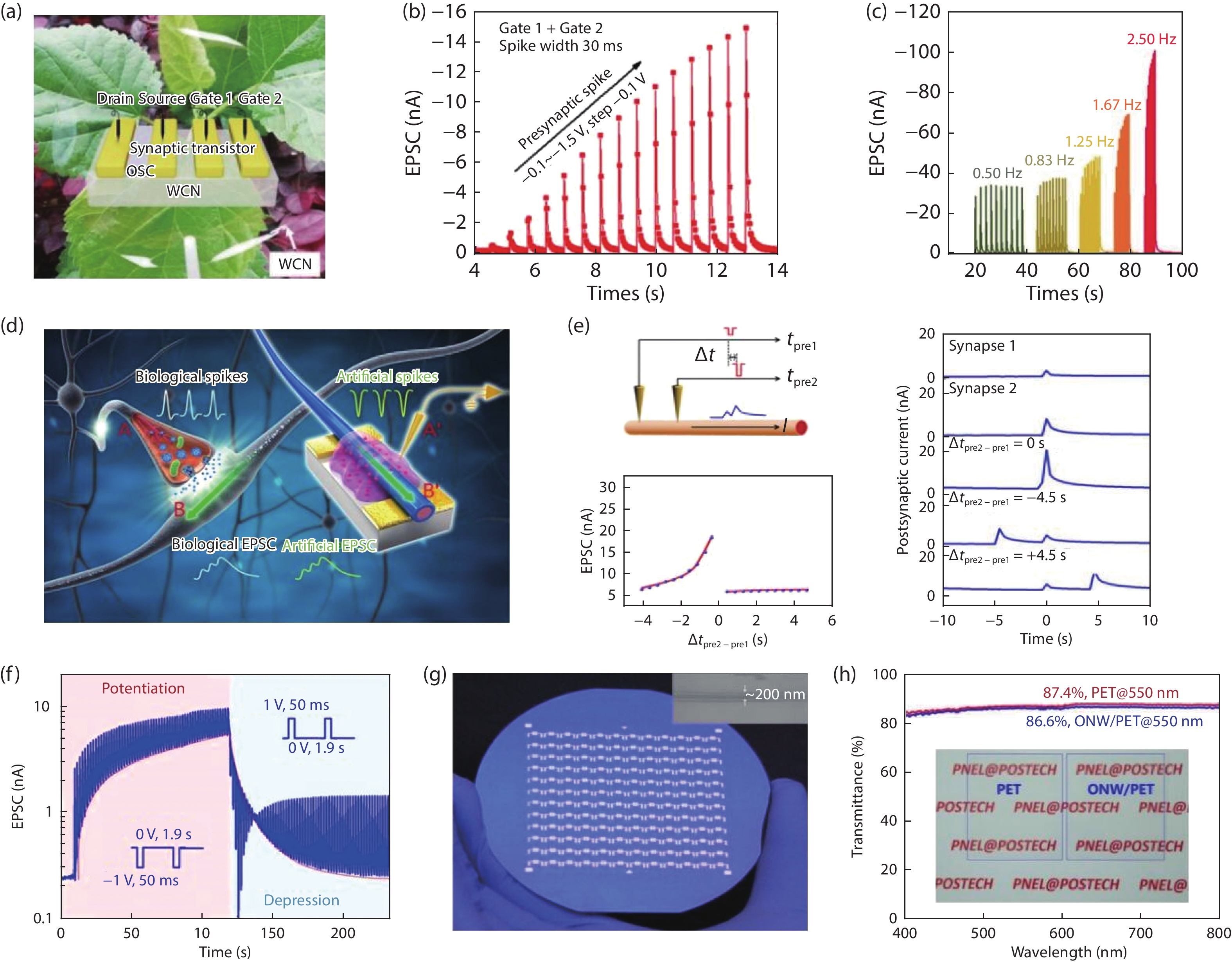
Von Neumann computers are currently failing to follow Moore’s law and are limited by the von Neumann bottleneck. To enhance computing performance, neuromorphic computing systems that can simulate the function of the human brain are being developed. Artificial synapses are essential electronic devices for neuromorphic architectures, which have the ability to perform signal processing and storage between neighboring artificial neurons. In recent years, electrolyte-gated transistors (EGTs) have been seen as promising devices in imitating synaptic dynamic plasticity and neuromorphic applications. Among the various electronic devices, EGT-based artificial synapses offer the benefits of good stability, ultra-high linearity and repeated cyclic symmetry, and can be constructed from a variety of materials. They also spatially separate “read” and “write” operations. In this article, we provide a review of the recent progress and major trends in the field of electrolyte-gated transistors for neuromorphic applications. We introduce the operation mechanisms of electric-double-layer and the structure of EGT-based artificial synapses. Then, we review different types of channels and electrolyte materials for EGT-based artificial synapses. Finally, we review the potential applications in biological functions.

J. Semicond.
2021, 42(1): 013104 doi: 10.1088/1674-4926/42/1/013104
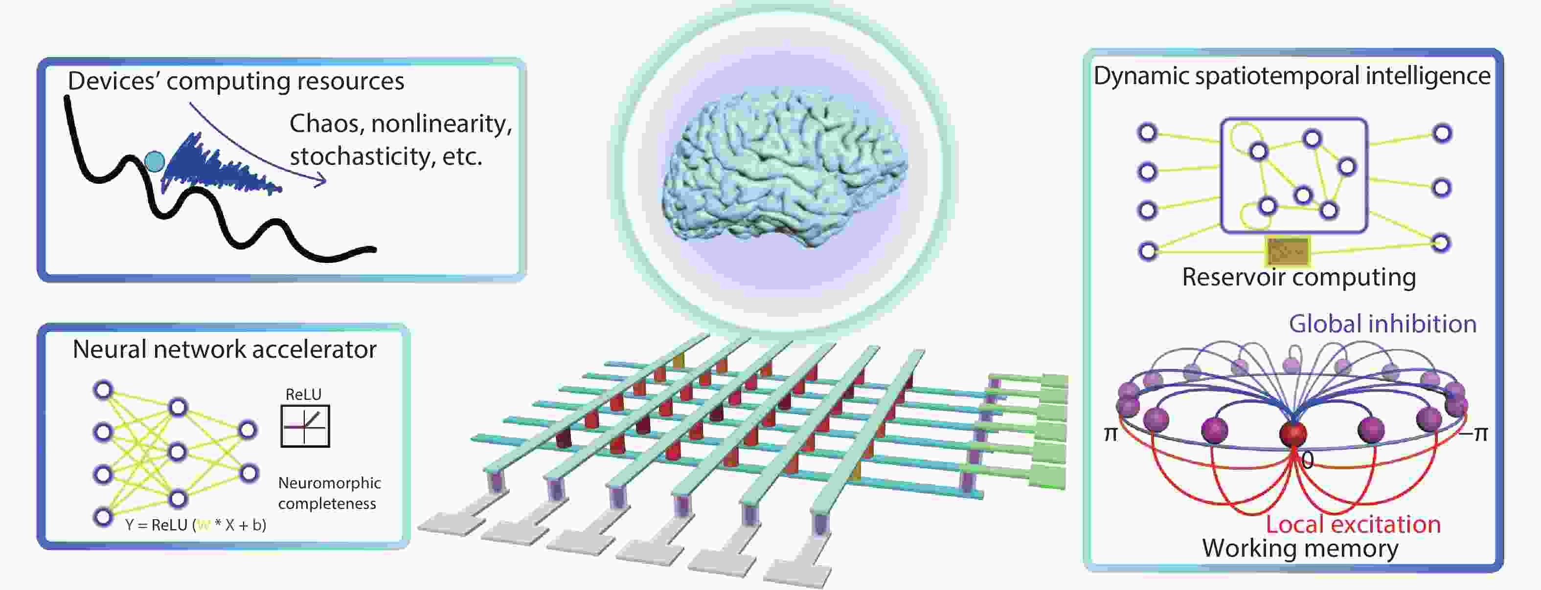
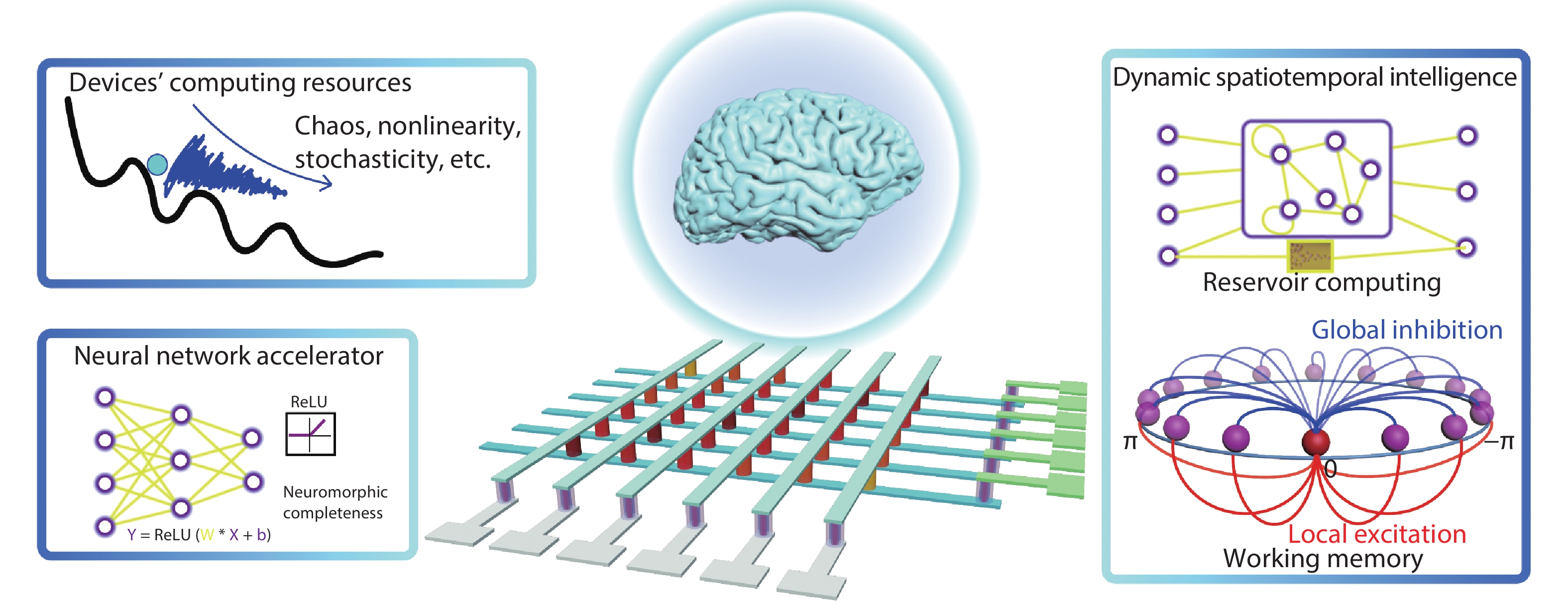
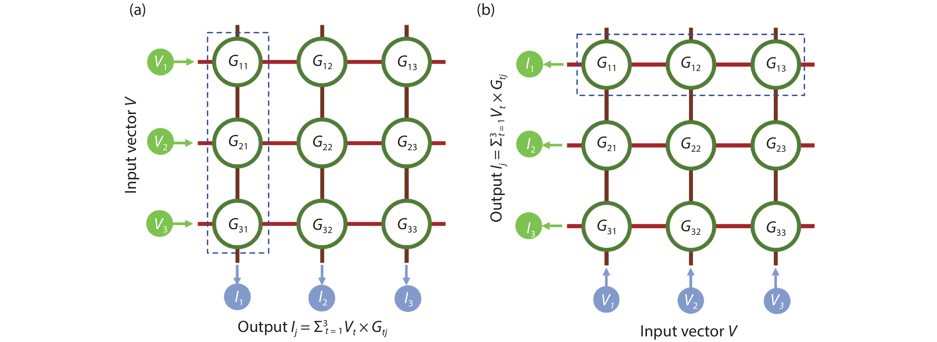
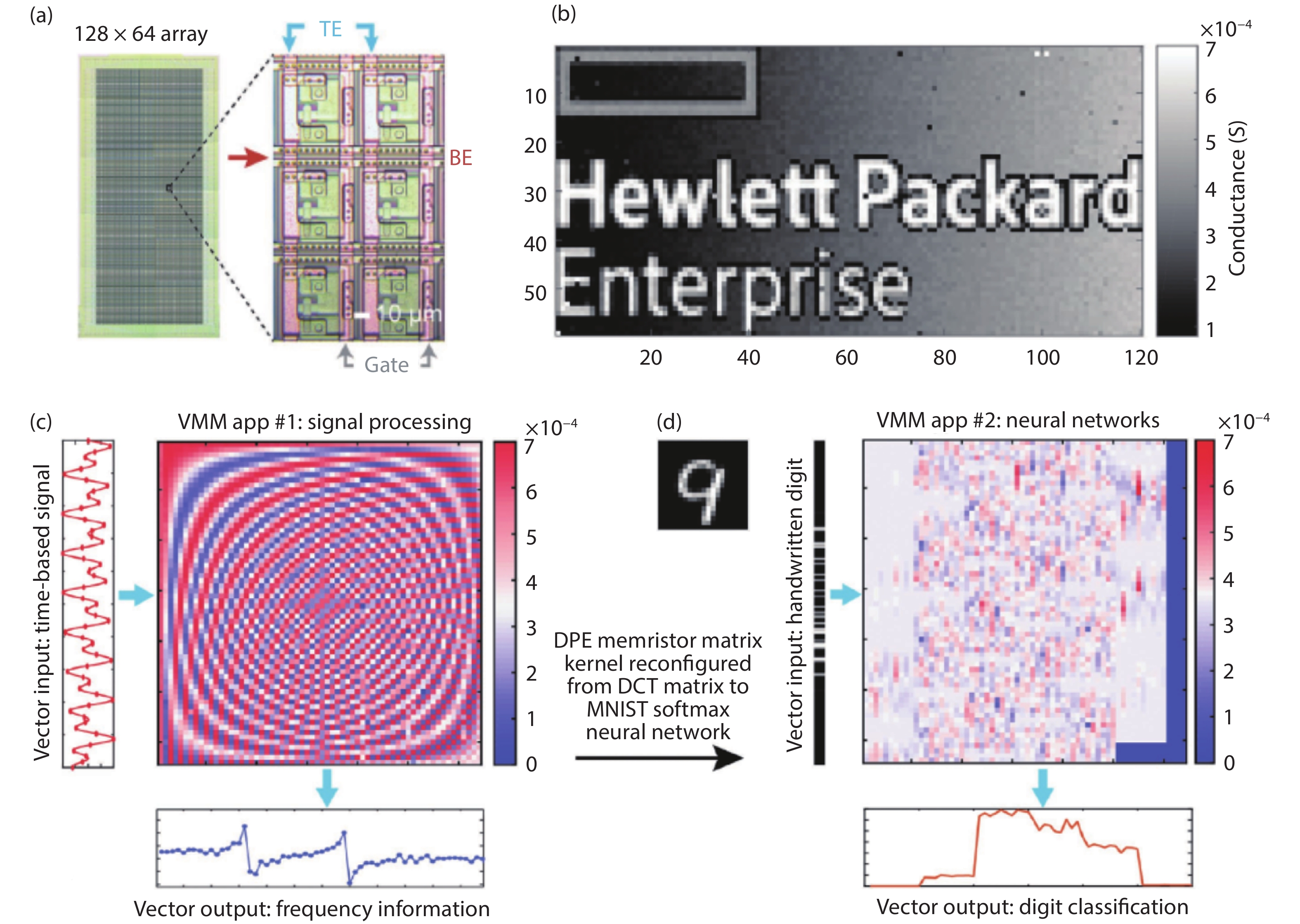
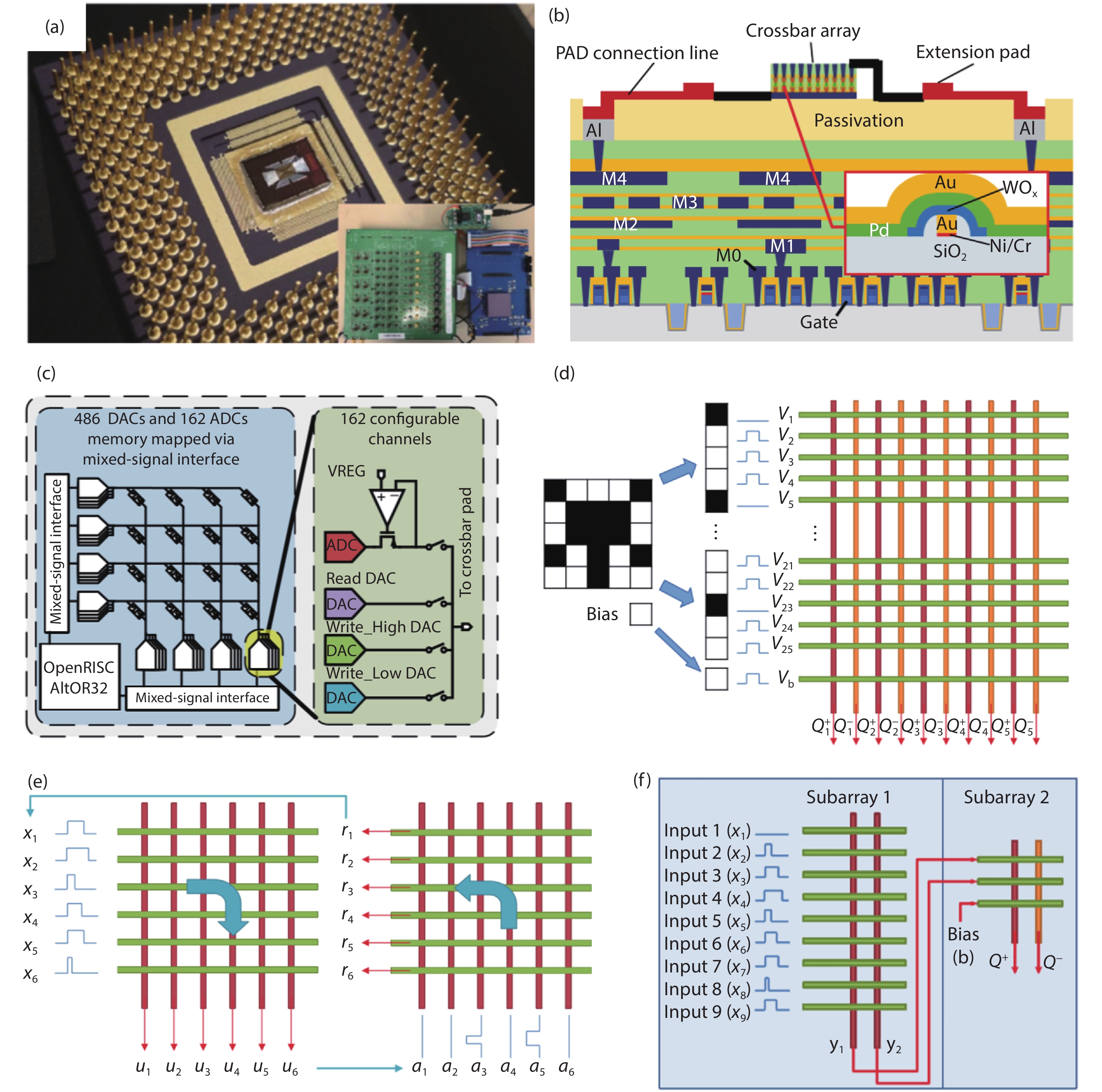
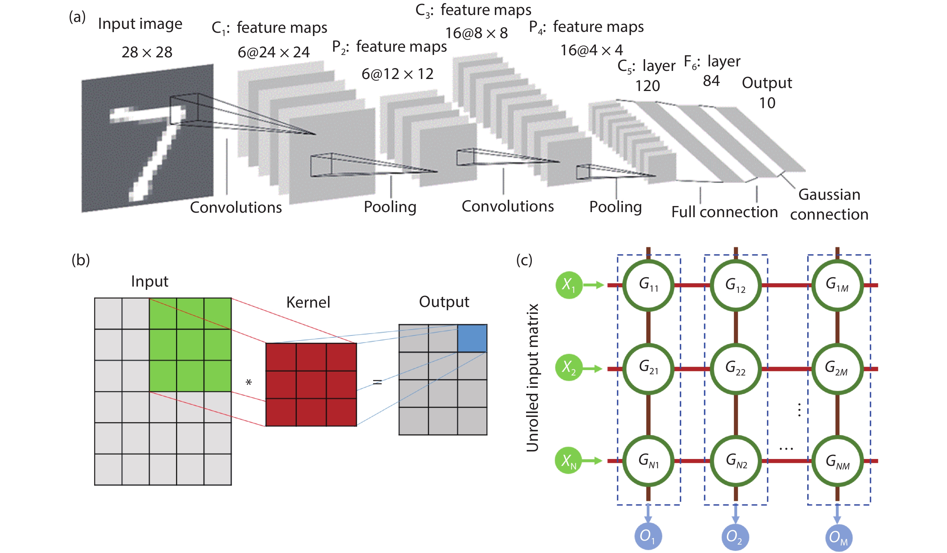
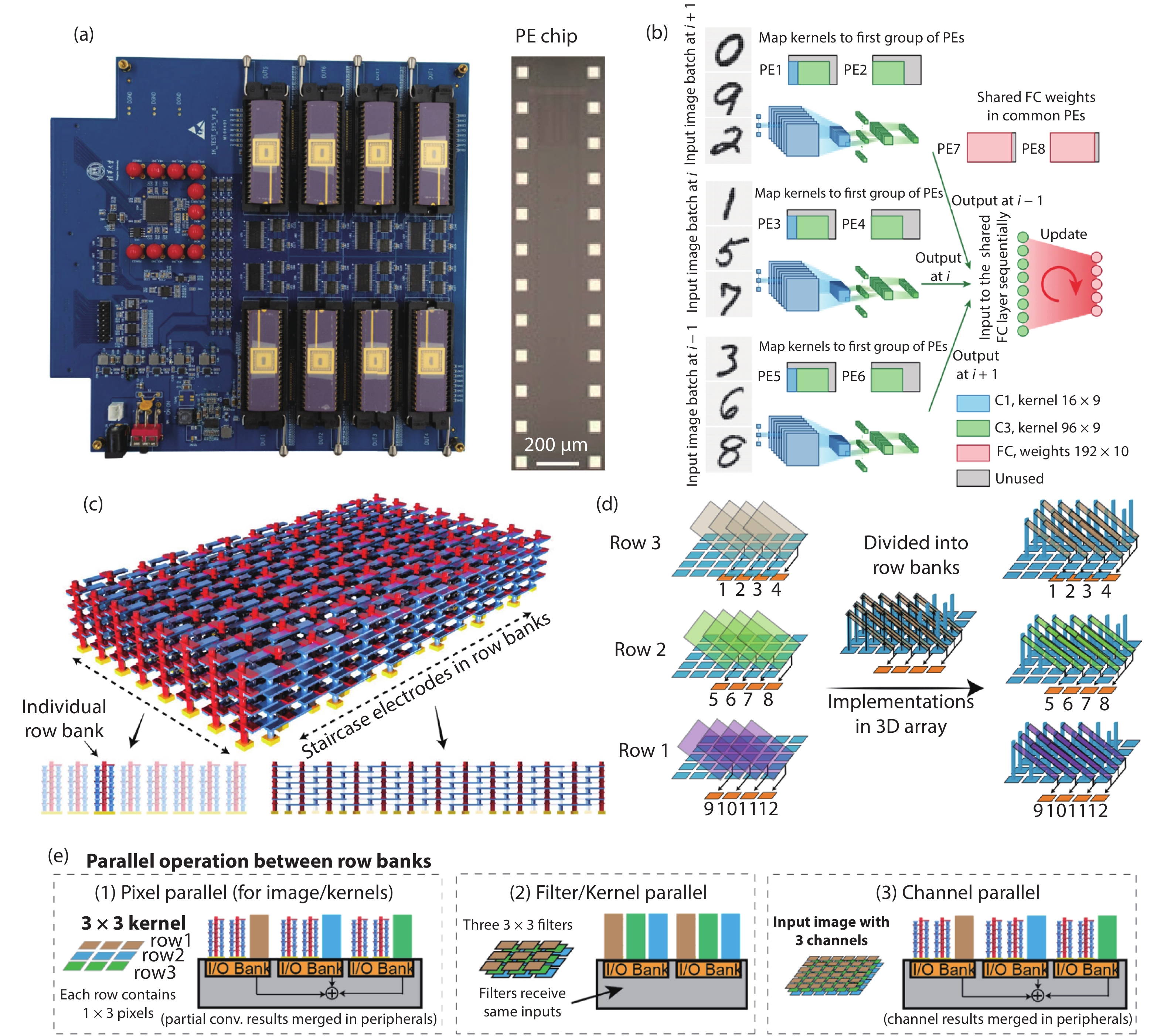
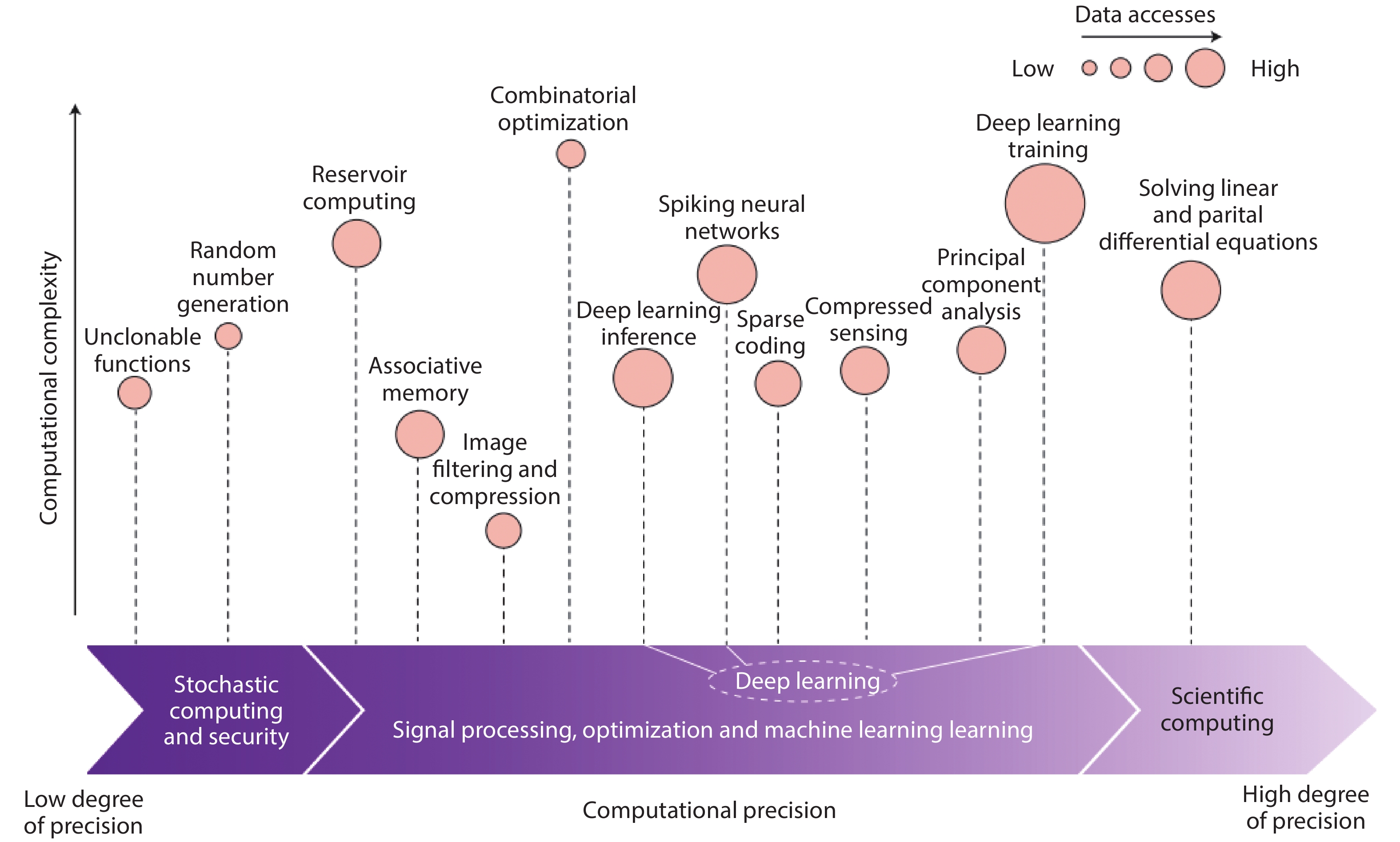
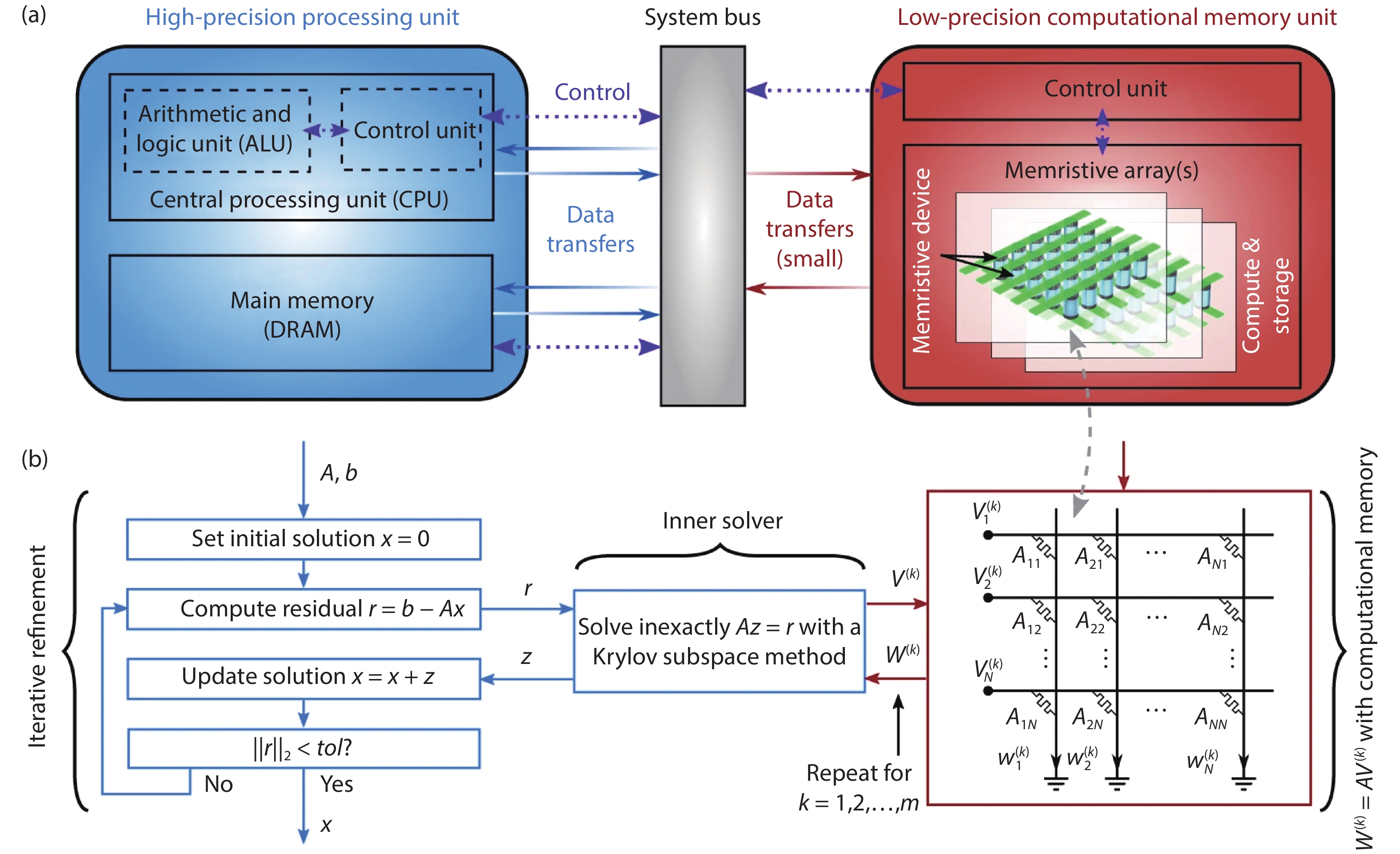
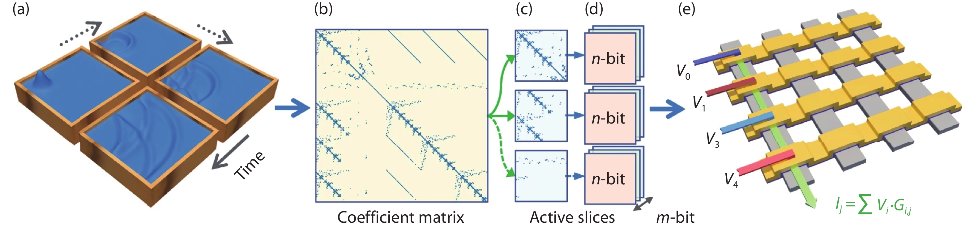
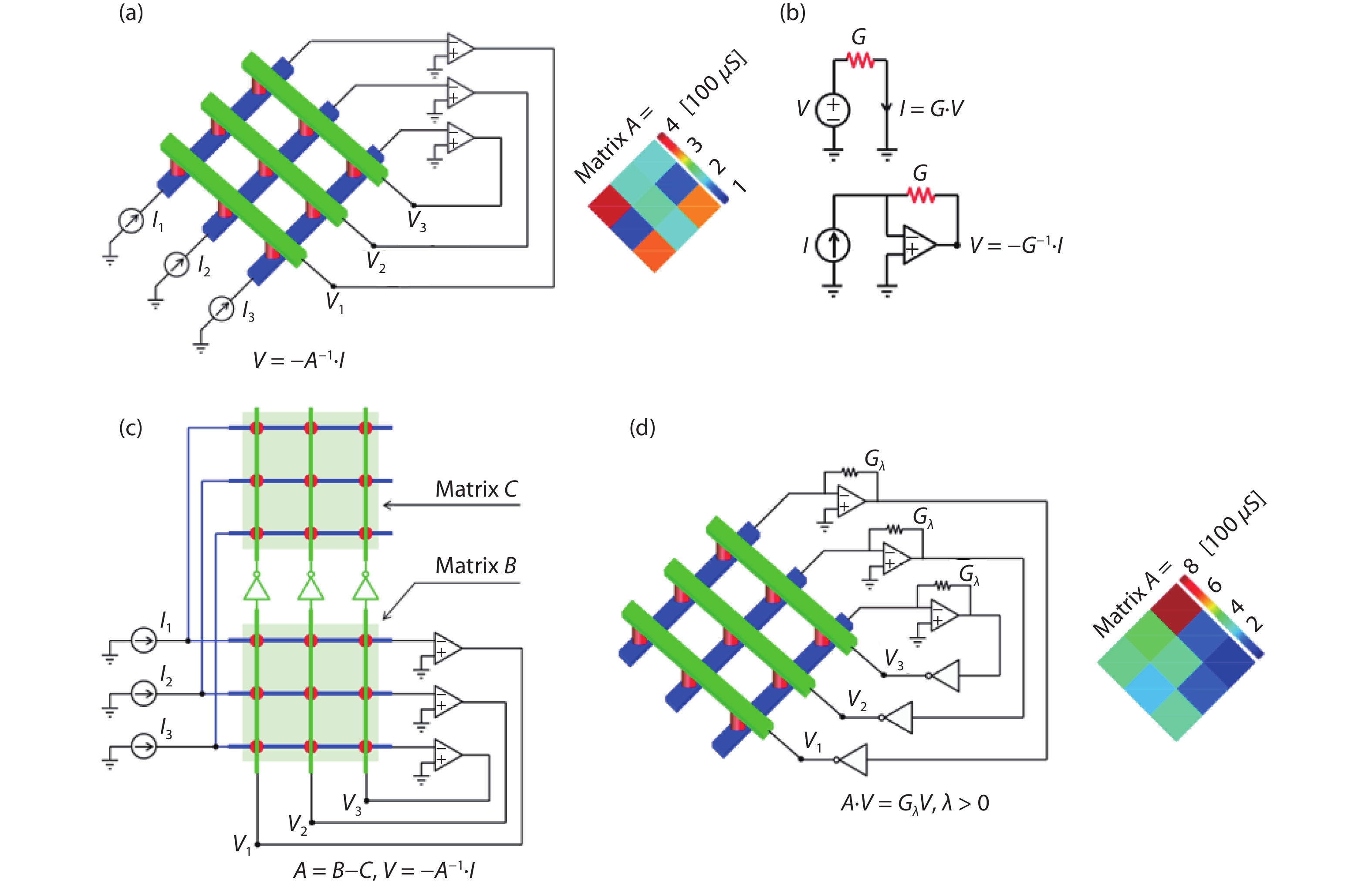
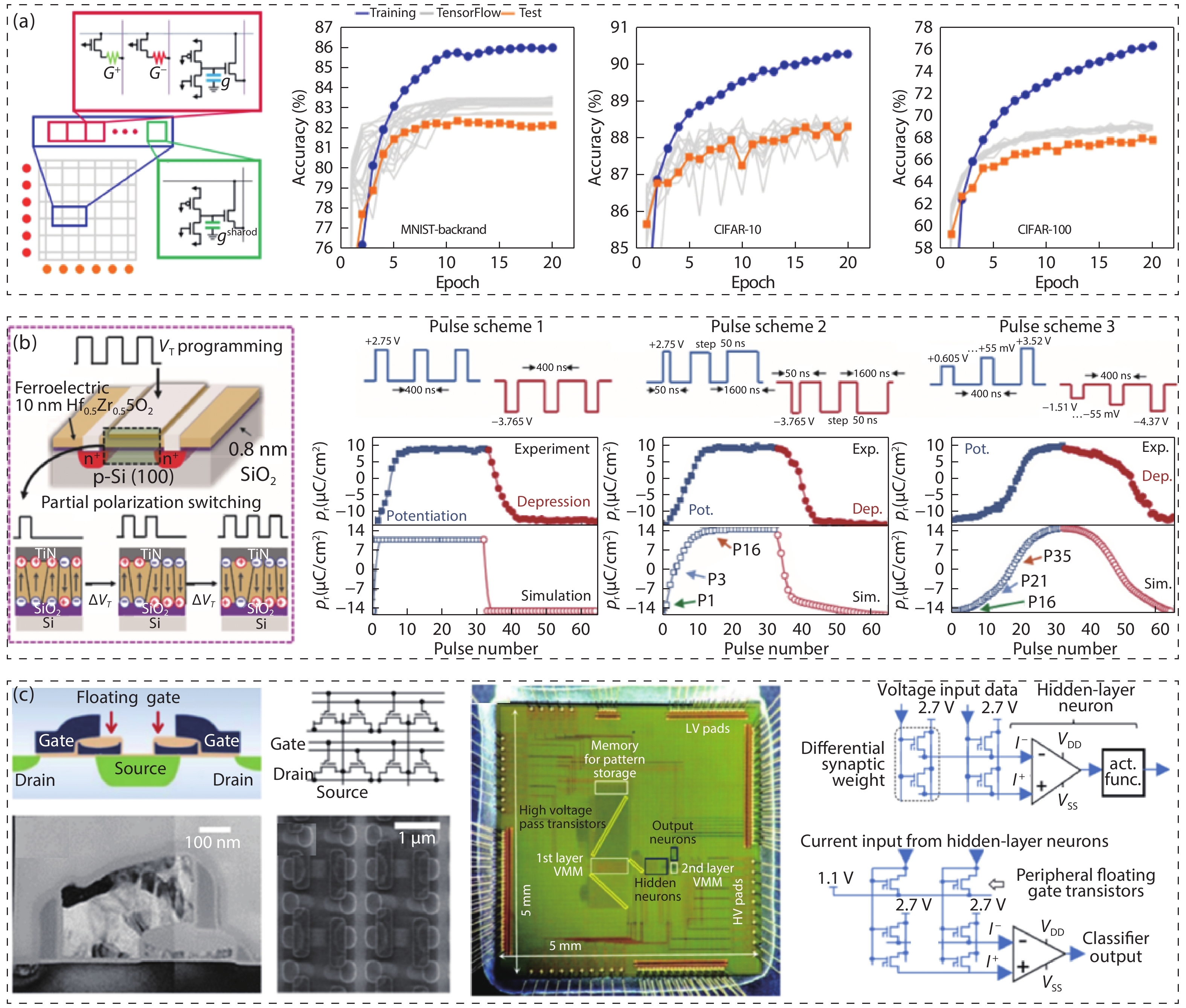
Memristors are now becoming a prominent candidate to serve as the building blocks of non-von Neumann in-memory computing architectures. By mapping analog numerical matrices into memristor crossbar arrays, efficient multiply accumulate operations can be performed in a massively parallel fashion using the physics mechanisms of Ohm’s law and Kirchhoff’s law. In this brief review, we present the recent progress in two niche applications: neural network accelerators and numerical computing units, mainly focusing on the advances in hardware demonstrations. The former one is regarded as soft computing since it can tolerant some degree of the device and array imperfections. The acceleration of multiple layer perceptrons, convolutional neural networks, generative adversarial networks, and long short-term memory neural networks are described. The latter one is hard computing because the solving of numerical problems requires high-precision devices. Several breakthroughs in memristive equation solvers with improved computation accuracies are highlighted. Besides, other nonvolatile devices with the capability of analog computing are also briefly introduced. Finally, we conclude the review with discussions on the challenges and opportunities for future research toward realizing memristive analog computing machines.


J. Semicond.
2021, 42(1): 013105 doi: 10.1088/1674-4926/42/1/013105
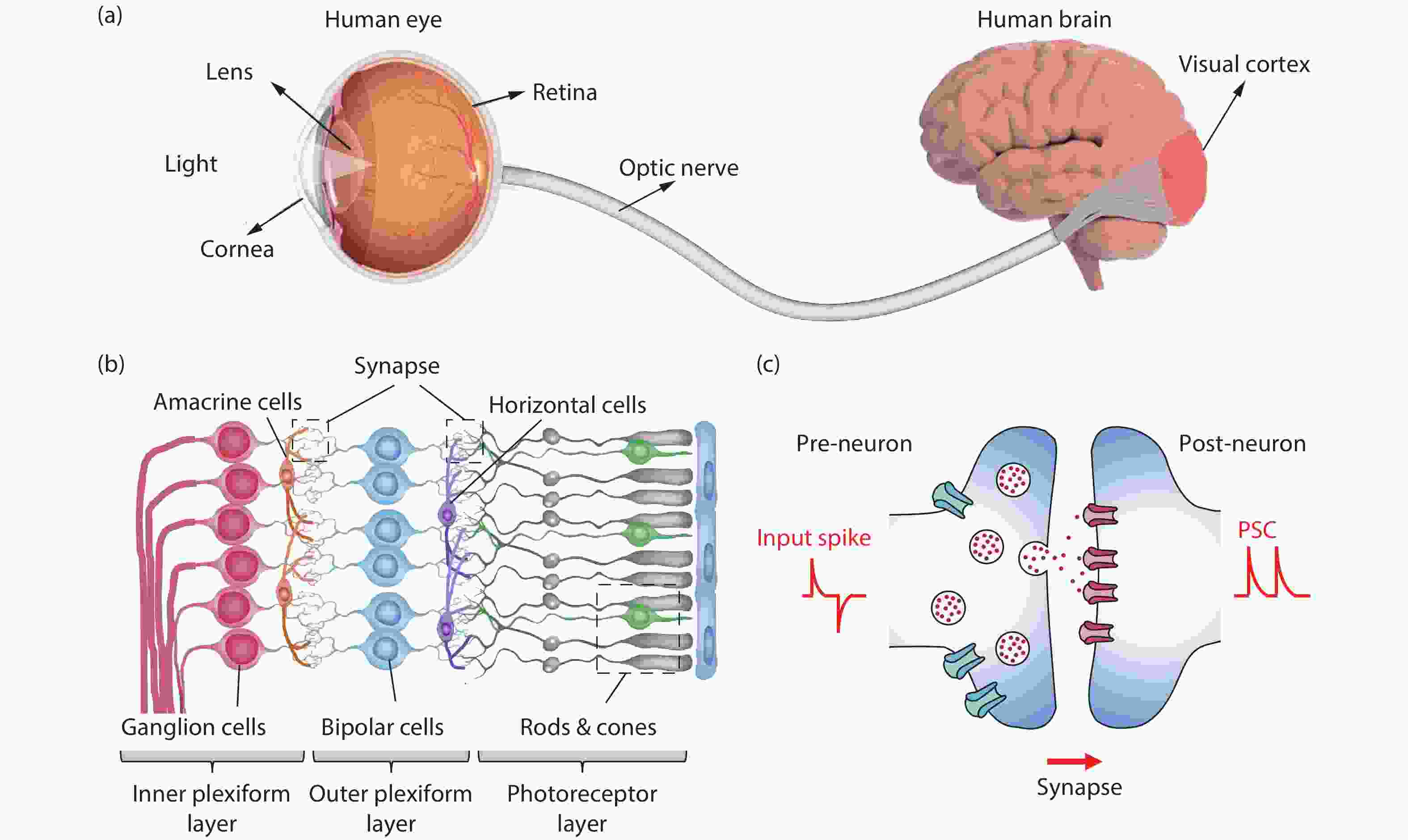
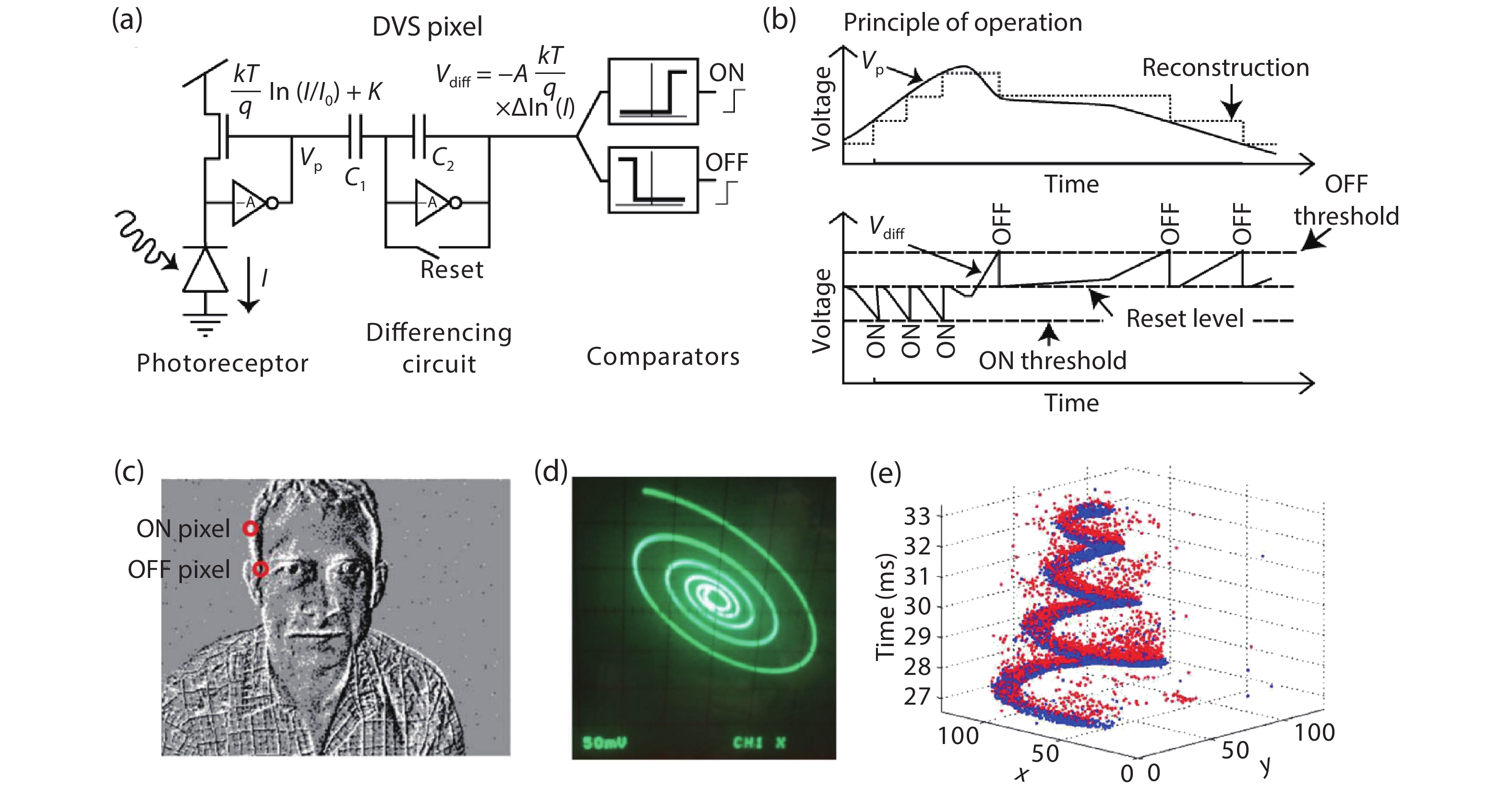
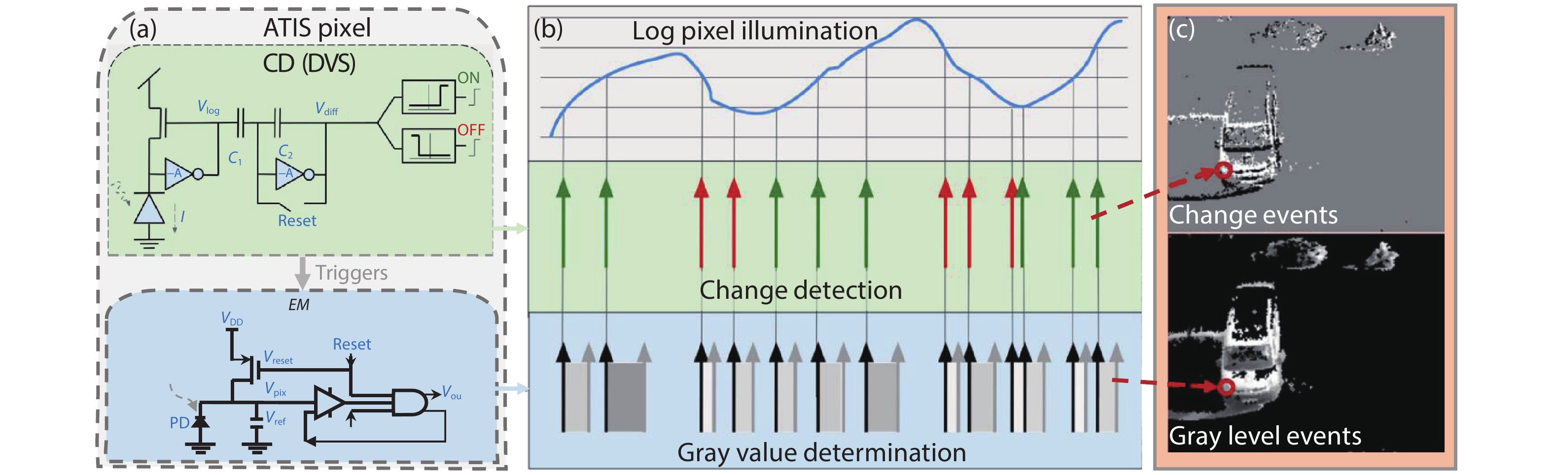
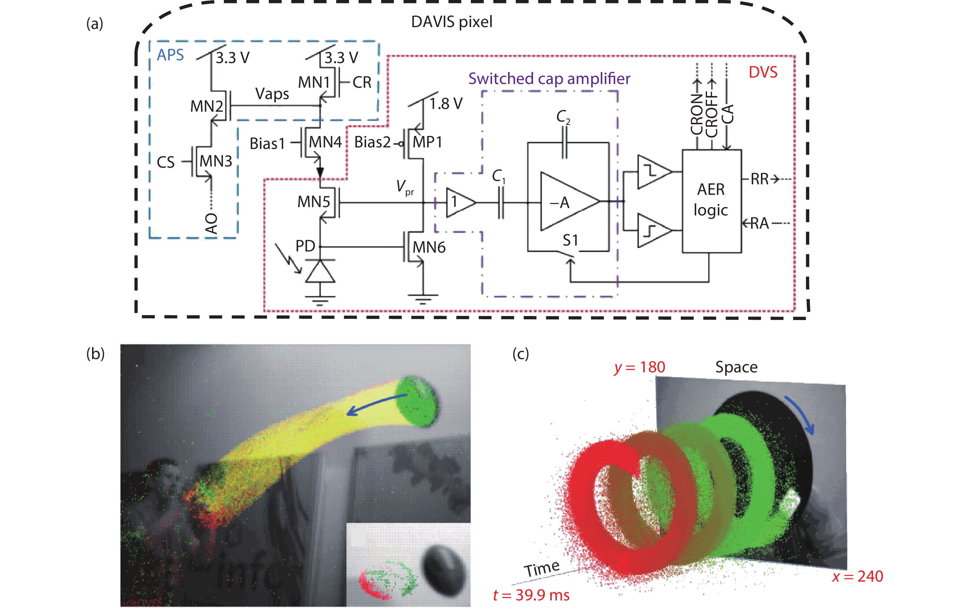
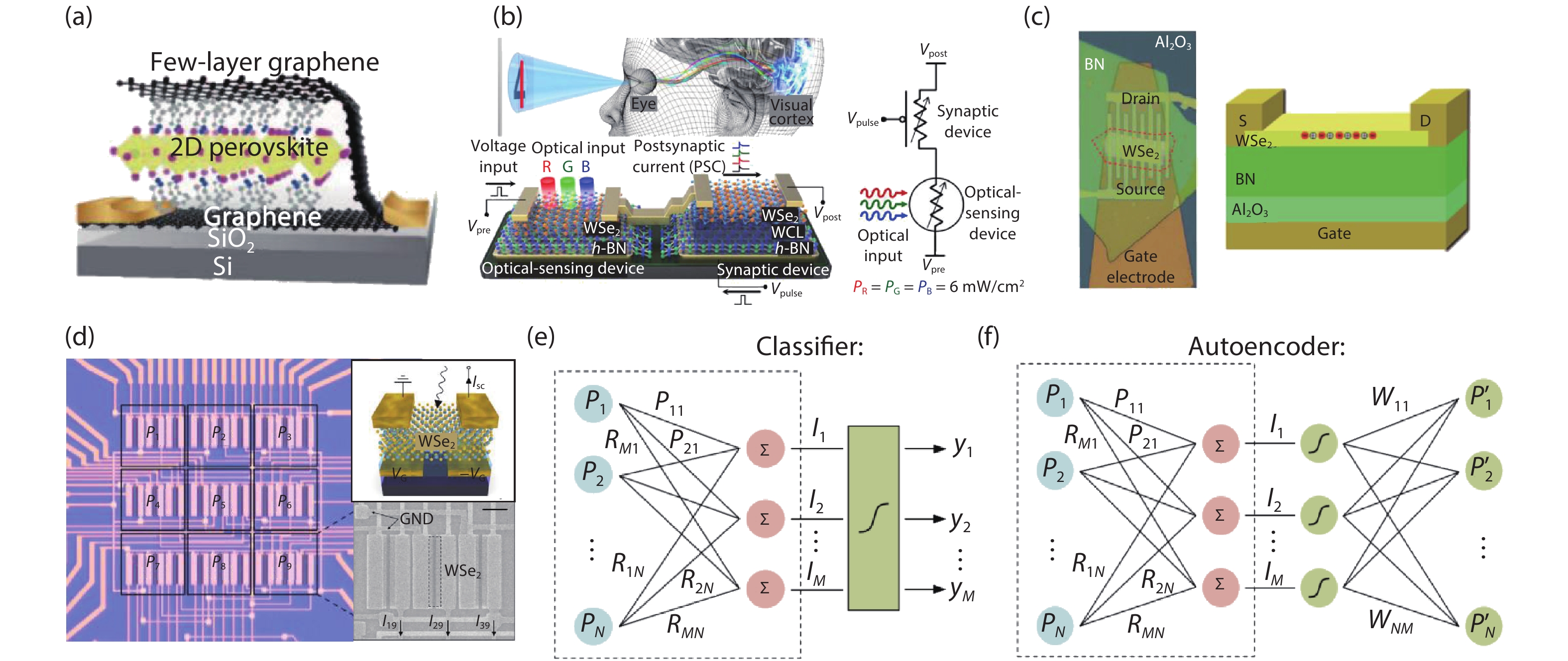
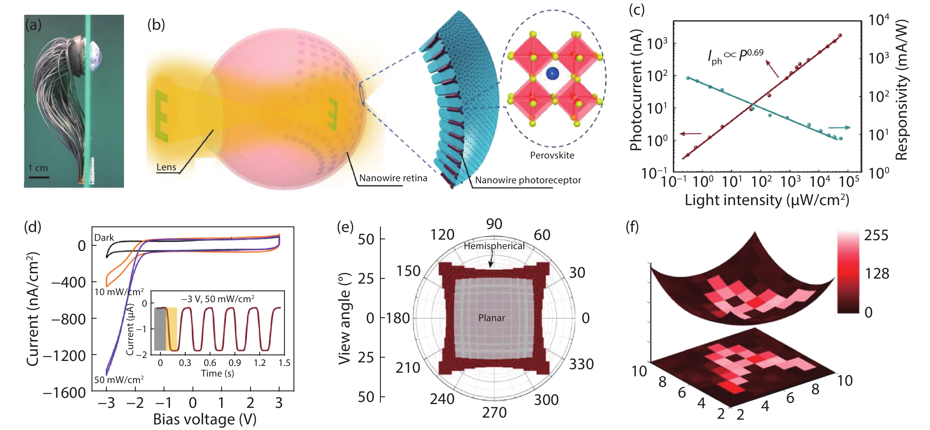
Conventional frame-based image sensors suffer greatly from high energy consumption and latency. Mimicking neurobiological structures and functionalities of the retina provides a promising way to build a neuromorphic vision sensor with highly efficient image processing. In this review article, we will start with a brief introduction to explain the working mechanism and the challenges of conventional frame-based image sensors, and introduce the structure and functions of biological retina. In the main section, we will overview recent developments in neuromorphic vision sensors, including the silicon retina based on conventional Si CMOS digital technologies, and the neuromorphic vision sensors with the implementation of emerging devices. Finally, we will provide a brief outline of the prospects and outlook for the development of this field.


J. Semicond.
2021, 42(1): 014101 doi: 10.1088/1674-4926/42/1/014101
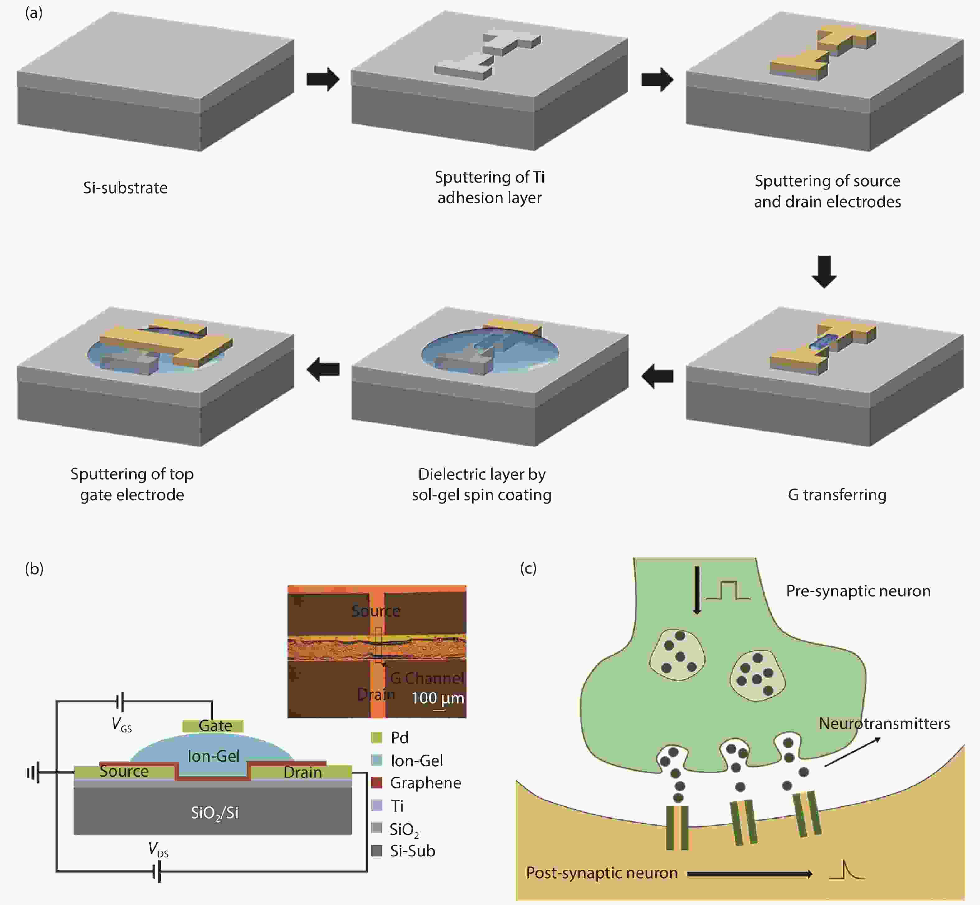
Multi-terminal electric-double-layer transistors have recently attracted extensive interest in terms of mimicking synaptic and neural functions. In this work, an Ion-Gel gated graphene synaptic transistor was proposed to mimic the essential synaptic behaviors by exploiting the bipolar property of graphene and the ionic conductivity of Ion-Gel. The Ion-Gel dielectrics were deposited onto the graphene film by the spin coating process. We consider the top gate and graphene channel as a presynaptic and postsynaptic terminal, respectively. Basic synaptic functions were successfully mimicked, including the excitatory postsynaptic current (EPSC), the effect of spike amplitude and duration on EPSC, and paired-pulse facilitation (PPF). This work may facilitate the application of graphene synaptic transistors in flexible electronics.

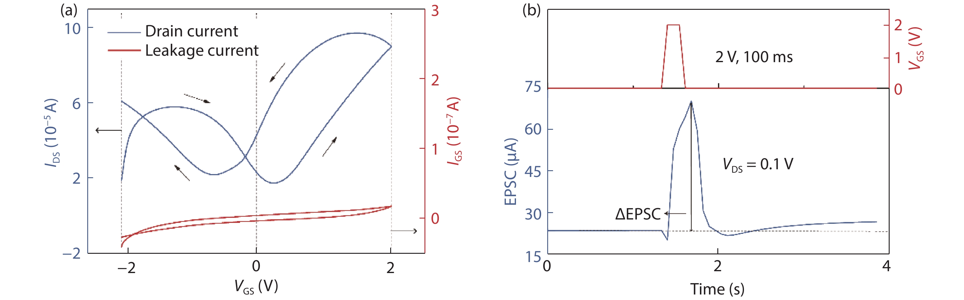

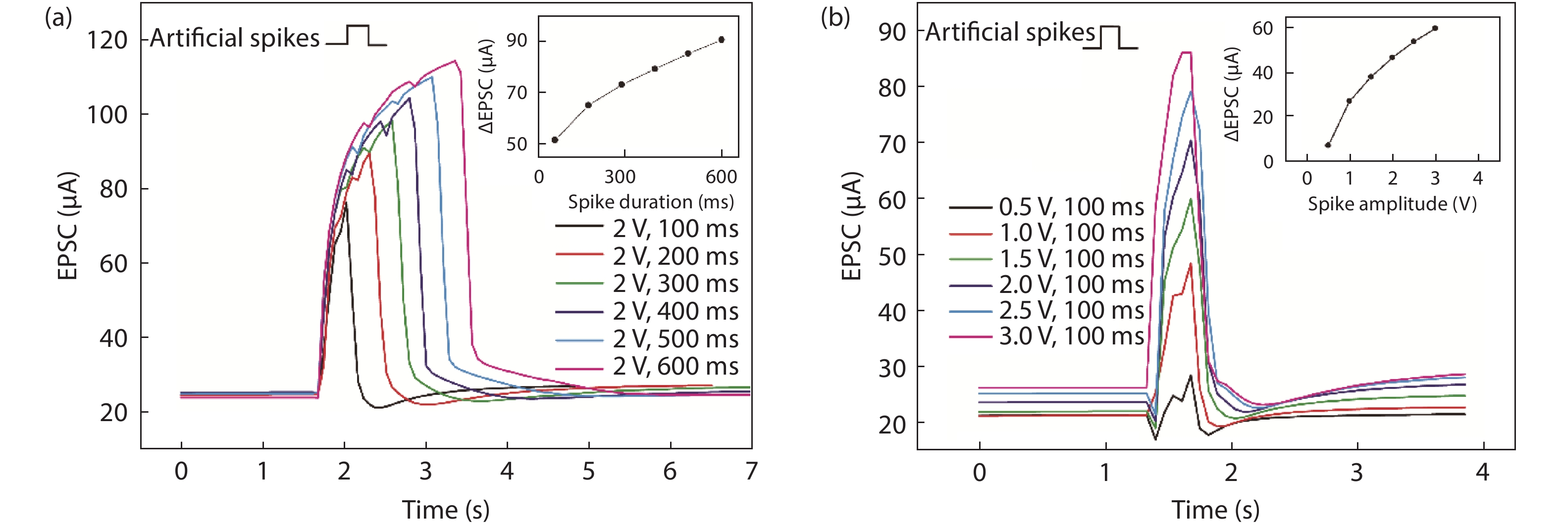
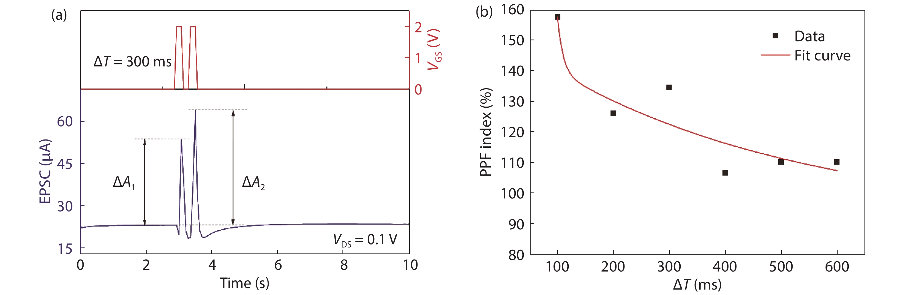
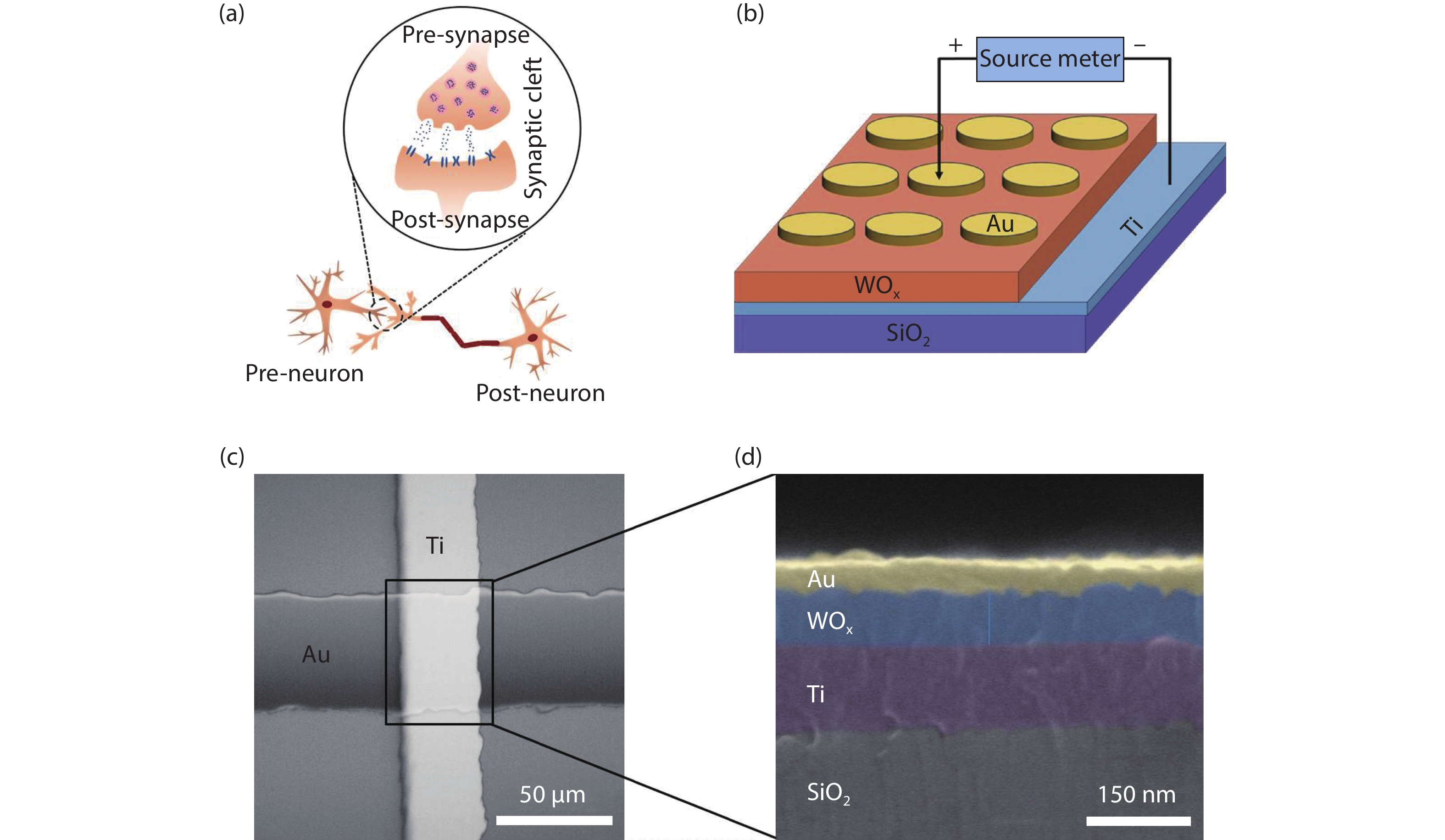
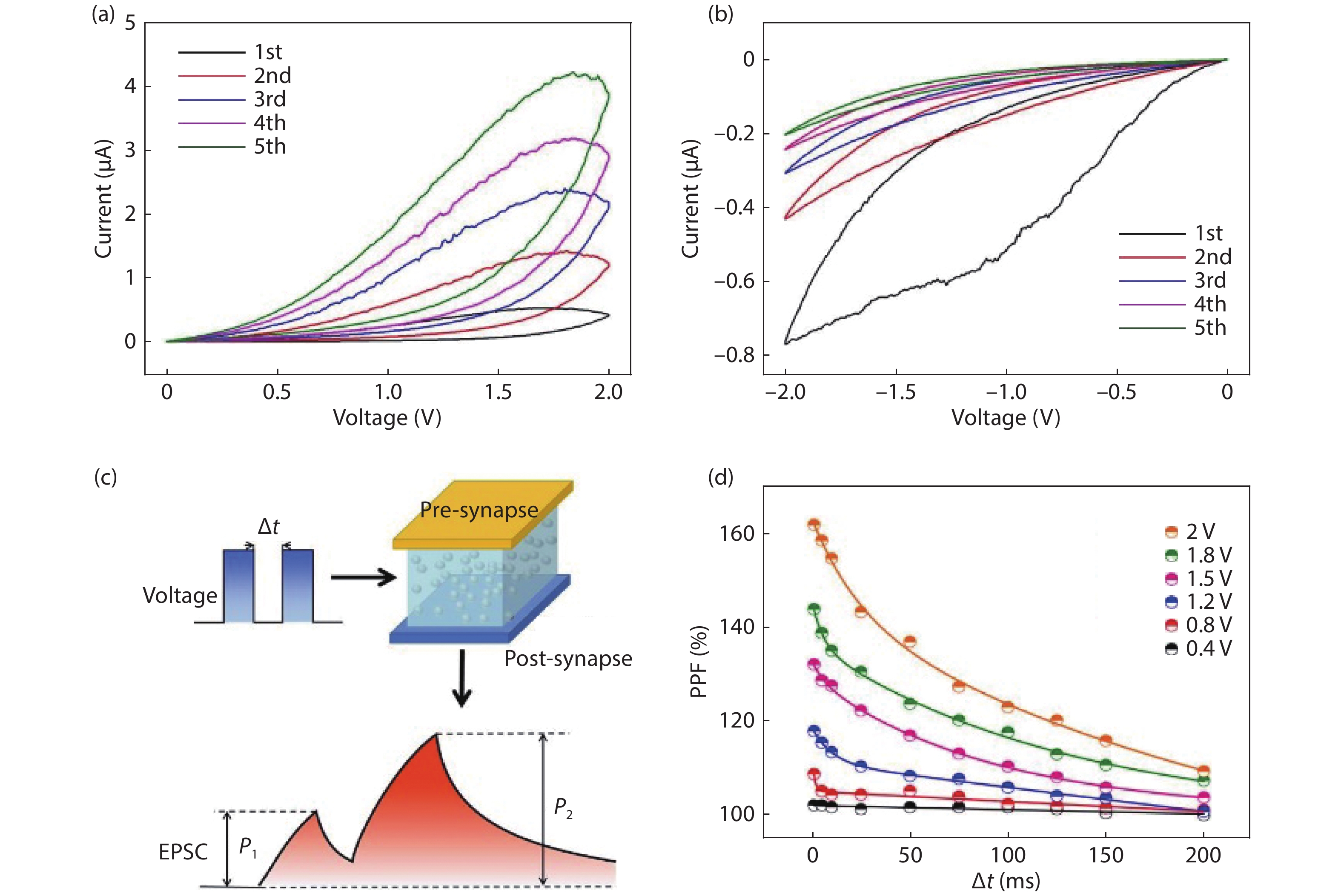
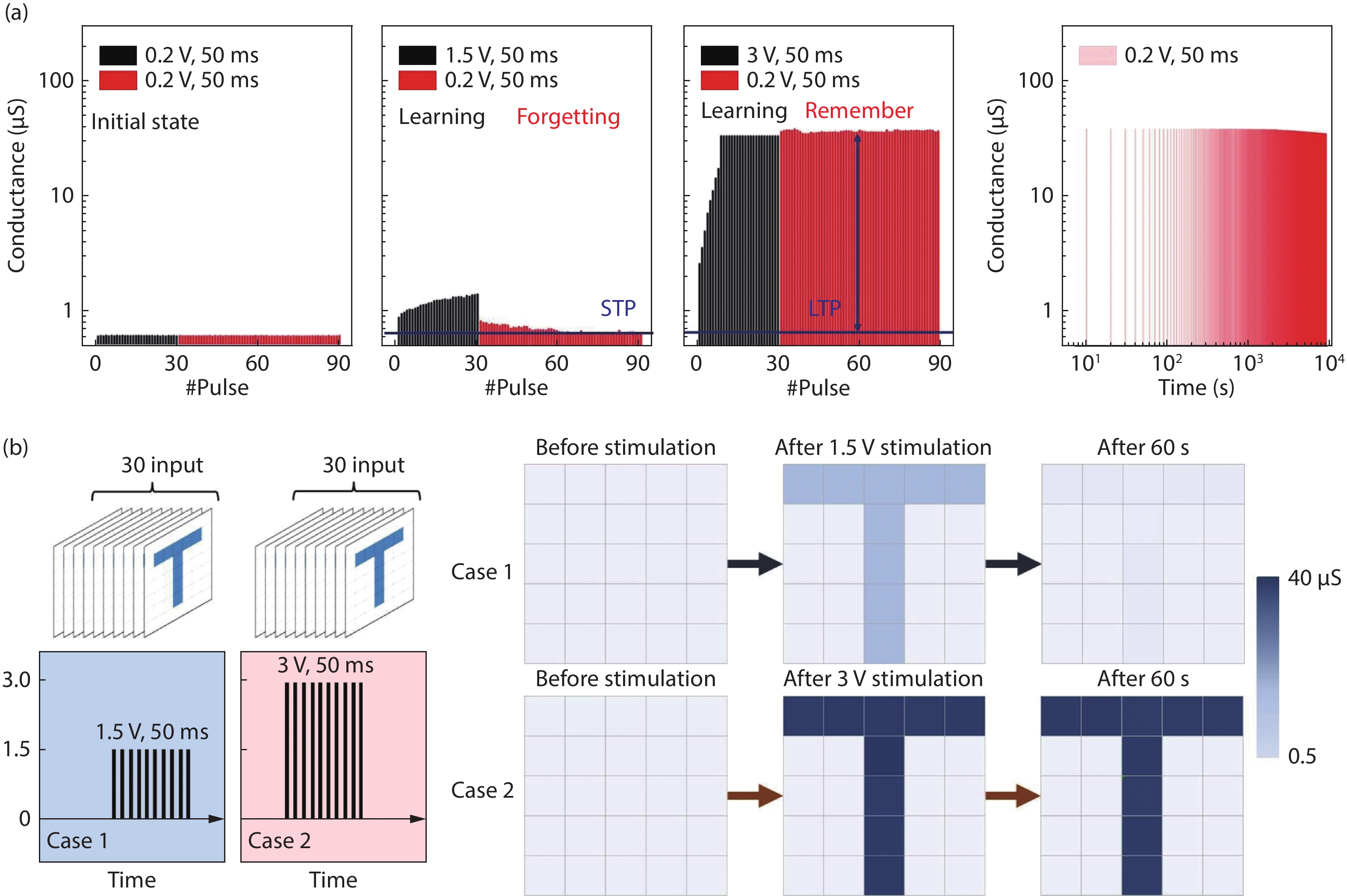
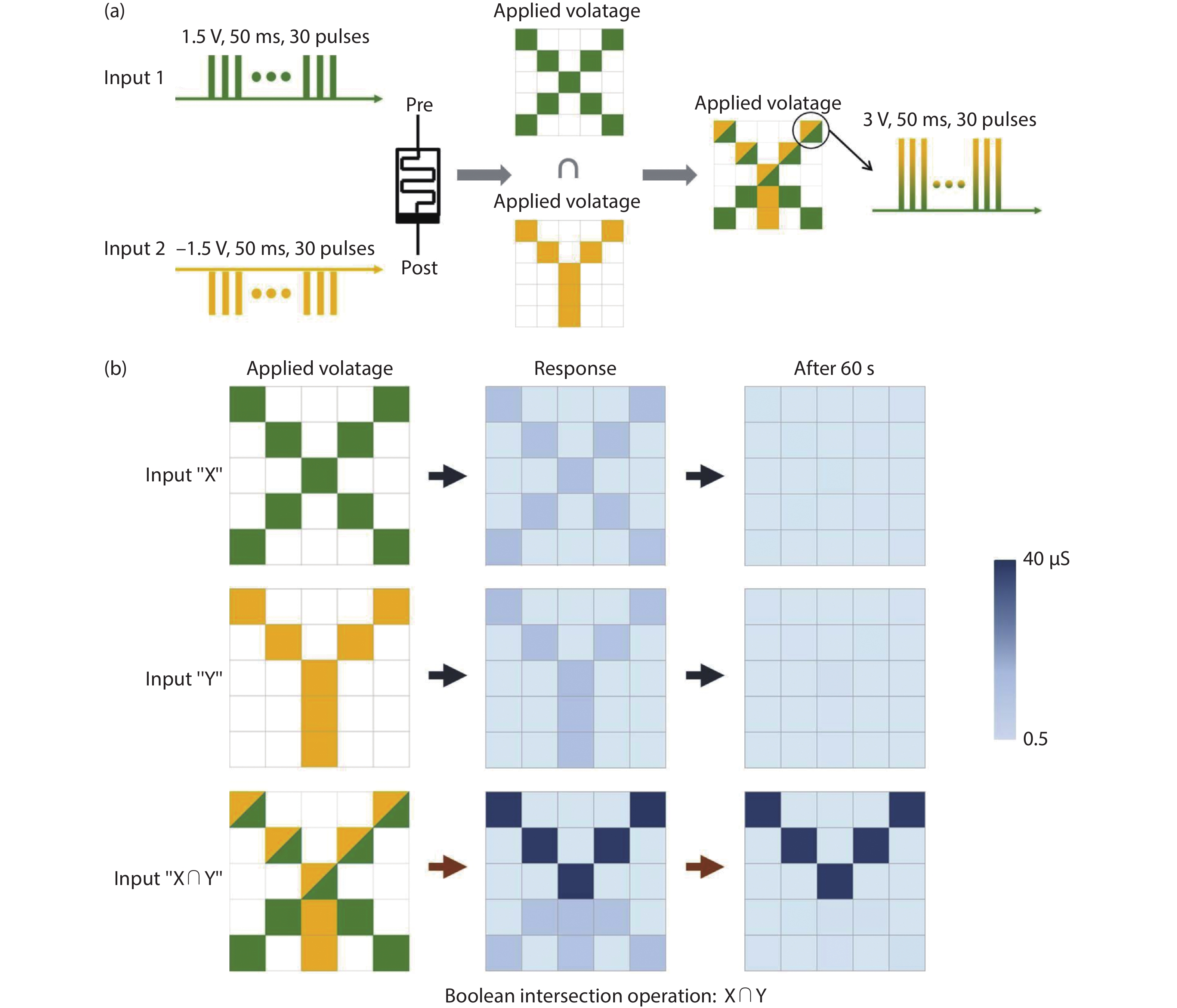
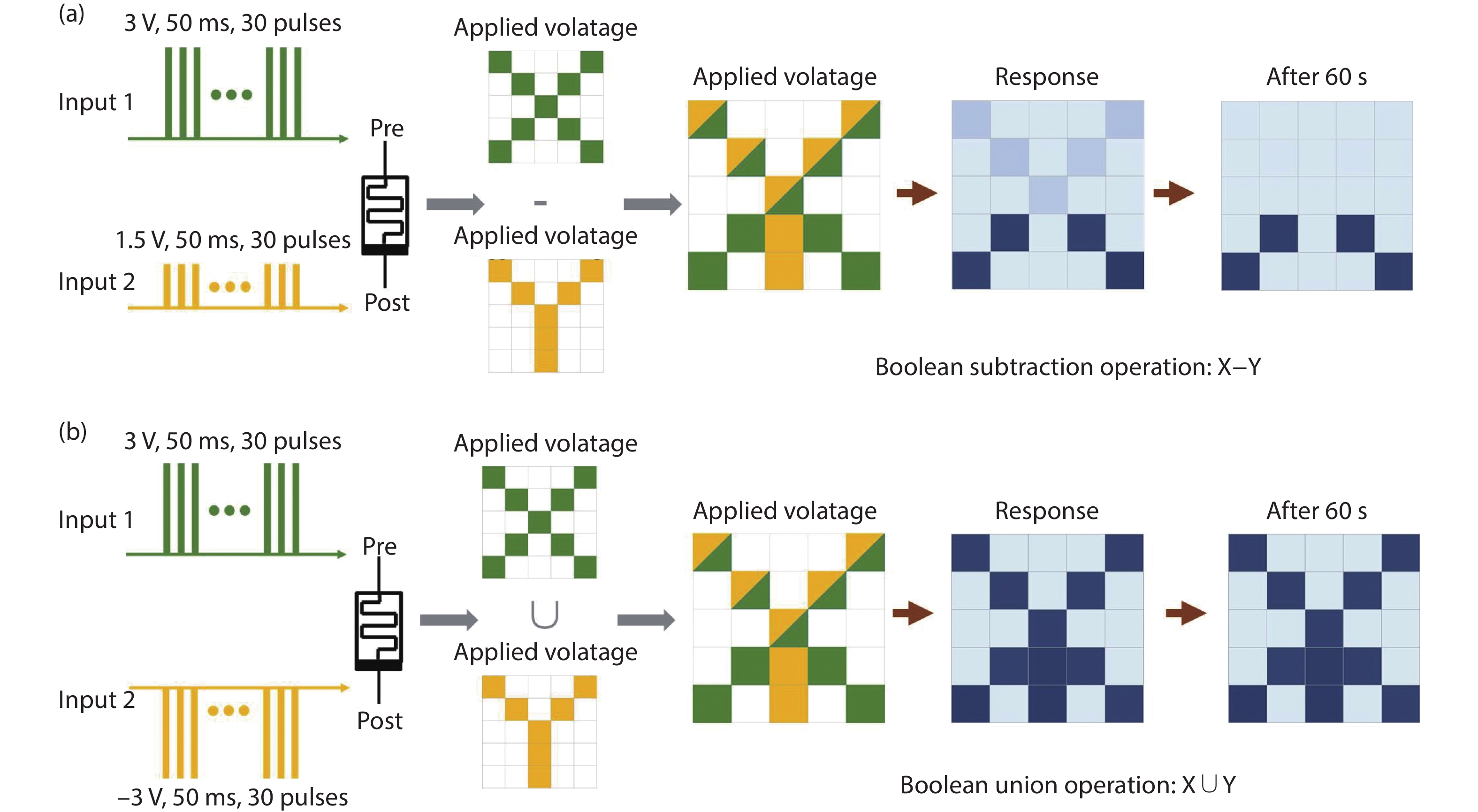
Voltage-dependent plasticity and image Boolean operations realized in a WOx-based memristive synapse
J. Semicond.
2021, 42(1): 014102 doi: 10.1088/1674-4926/42/1/014102
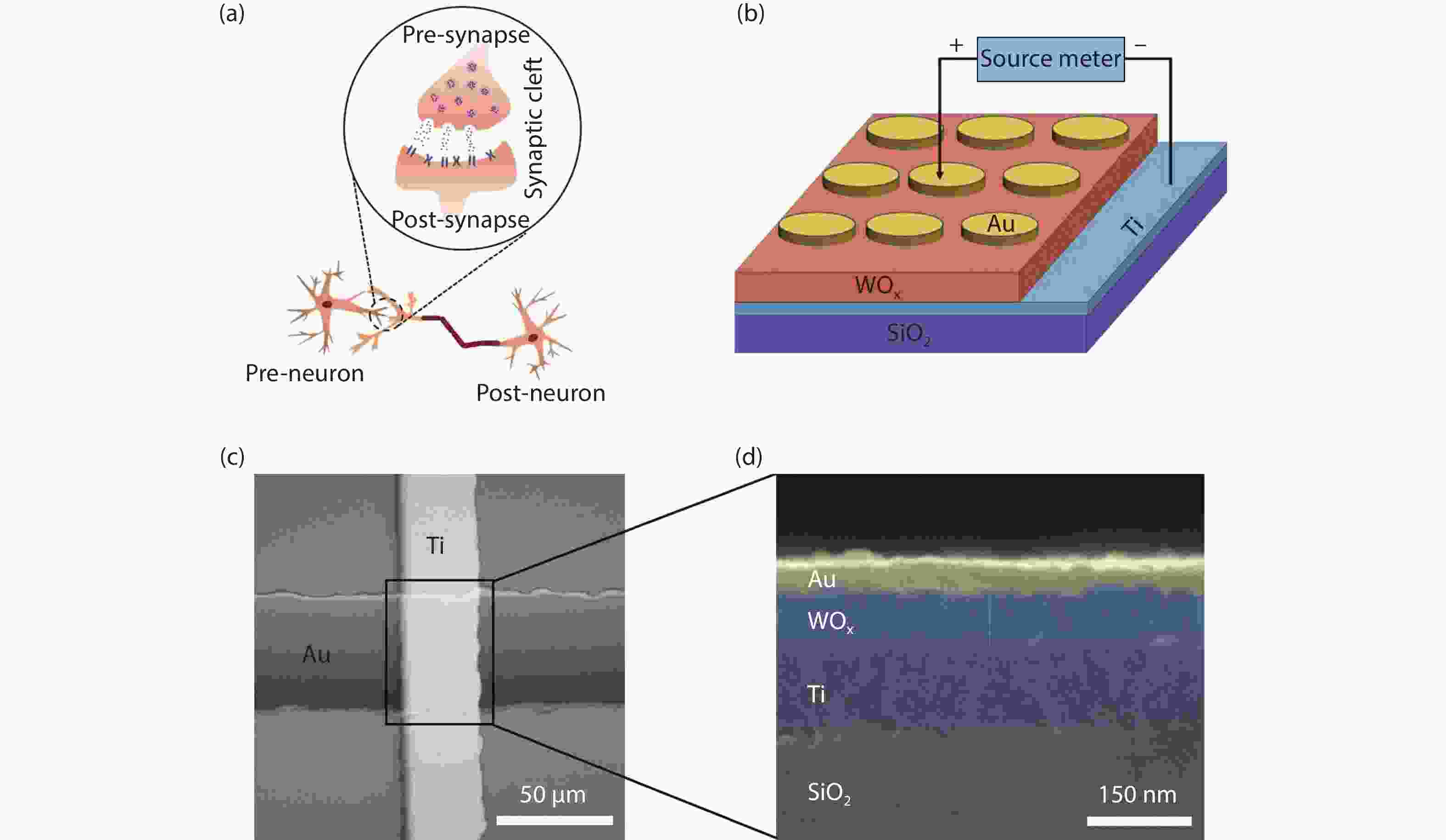
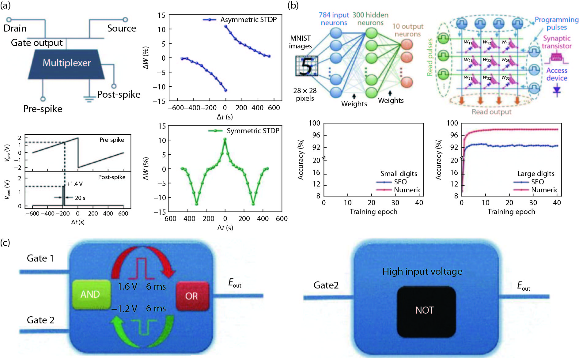
The development of electronic devices that possess the functionality of biological synapses is a crucial step towards neuromorphic computing. In this work, we present a WOx-based memristive device that can emulate voltage-dependent synaptic plasticity. By adjusting the amplitude of the applied voltage, we were able to reproduce short-term plasticity (STP) and the transition from STP to long-term potentiation. The stimulation with high intensity induced long-term enhancement of conductance without any decay process, thus representing a permanent memory behavior. Moreover, the image Boolean operations (including intersection, subtraction, and union) were also demonstrated in the memristive synapse array based on the above voltage-dependent plasticity. The experimental achievements of this study provide a new insight into the successful mimicry of essential characteristics of synaptic behaviors.
J. Semicond.
2021, 42(1): 014103 doi: 10.1088/1674-4926/42/1/014103
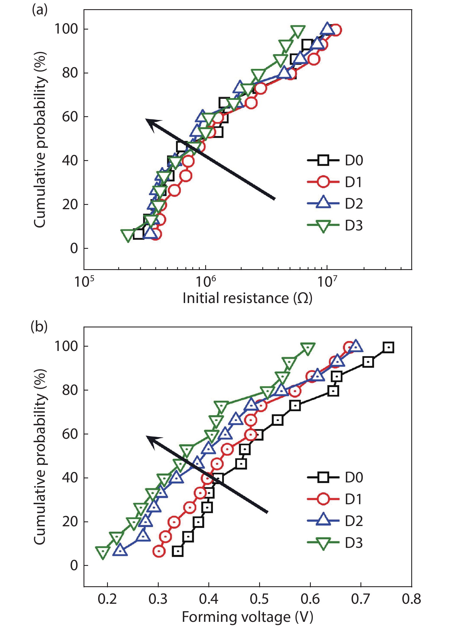
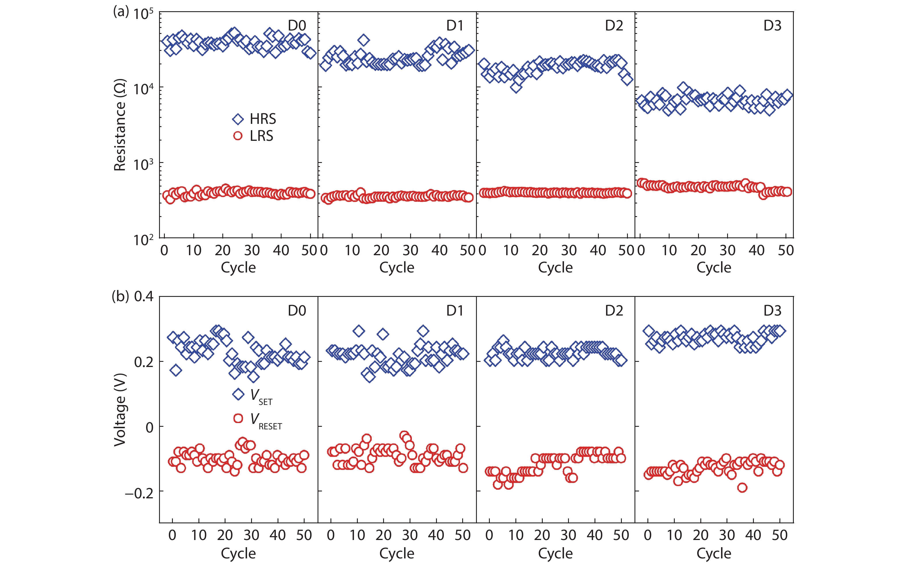
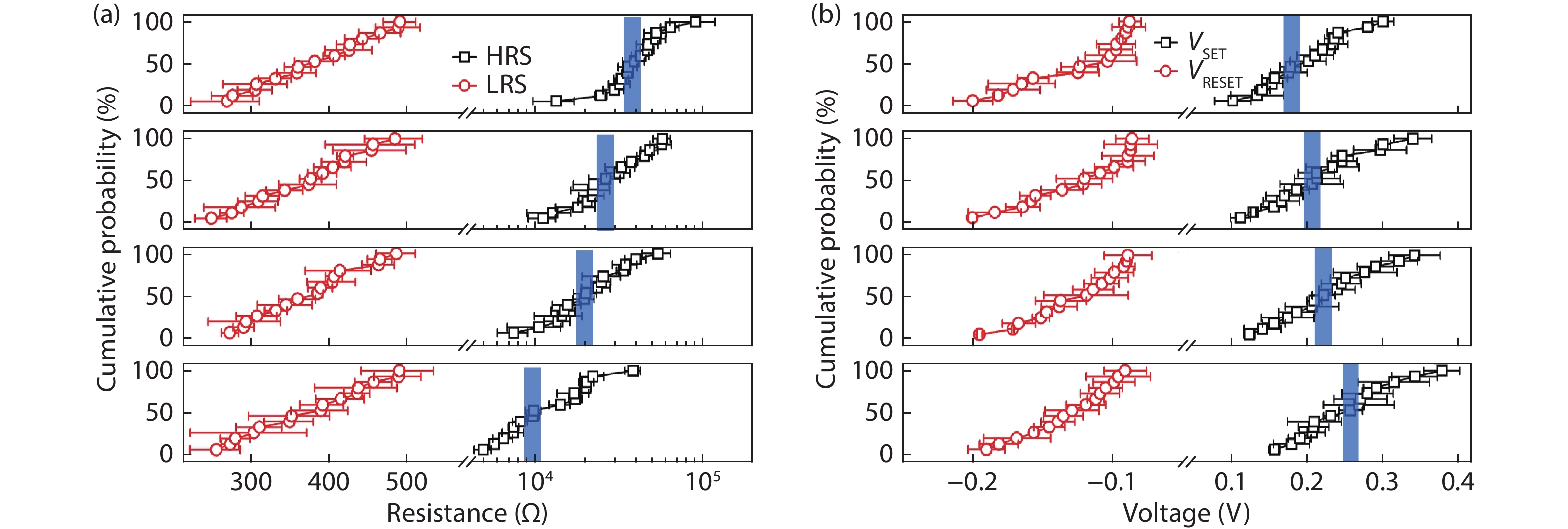
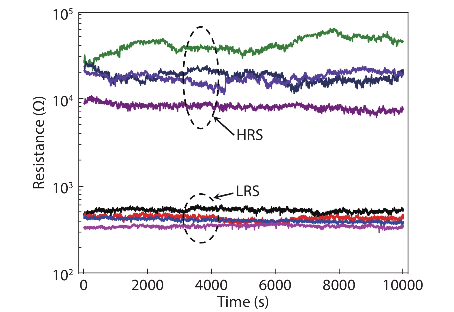
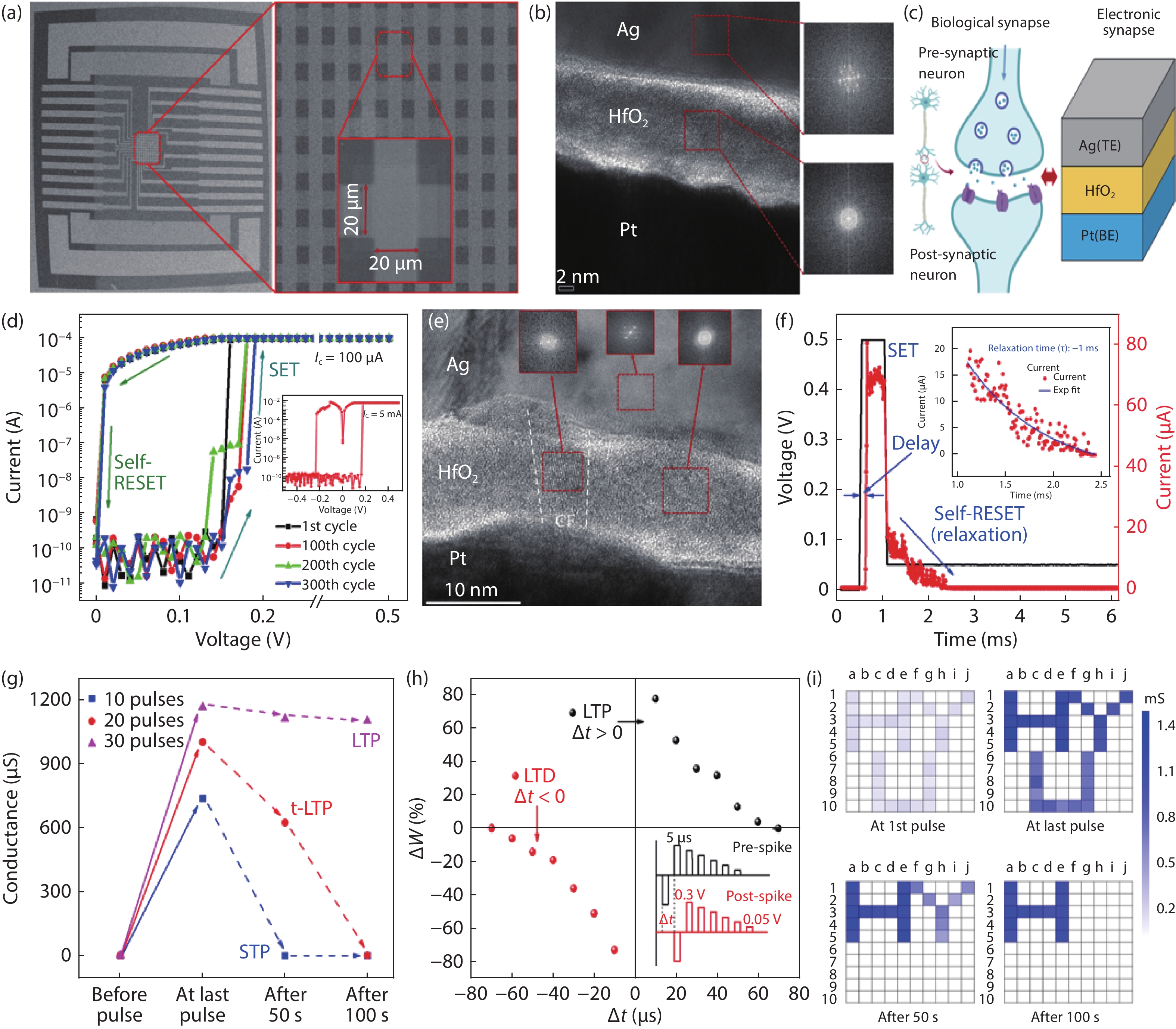
In this work, electrochemical metallization memory (ECM) devices with an Ag/AgInSbTe (AIST)/amorphous carbon (a-C)/Pt structure were irradiated with 14 MeV neutrons. The switching reliability performance before and after neutron irradiation was compared and analyzed in detail. The results show that the irradiated memory cells functioned properly, and the initial resistance, the resistance at the low-resistance state (LRS), the RESET voltage and the data retention performance showed little degradation even when the total neutron fluence was as high as 2.5 × 10¹¹ n/cm2. Other switching characteristics such as the forming voltage, the resistance at the high-resistance state (HRS), and the SET voltage were also studied, all of which merely showed a slight parameter drift. Irradiation-induced Ag ions doping of the a-C layer is proposed to explain the damaging effects of neutron irradiation. The excellent hard characteristics of these Ag/AIST/a-C/Pt-based ECM devices suggest potential beneficial applications in the aerospace and nuclear industries.