Issue Browser
Volume 43, Issue 12,
Dec 2022


J. Semicond.
2022, 43(12): 121201 doi: 10.1088/1674-4926/43/12/121201
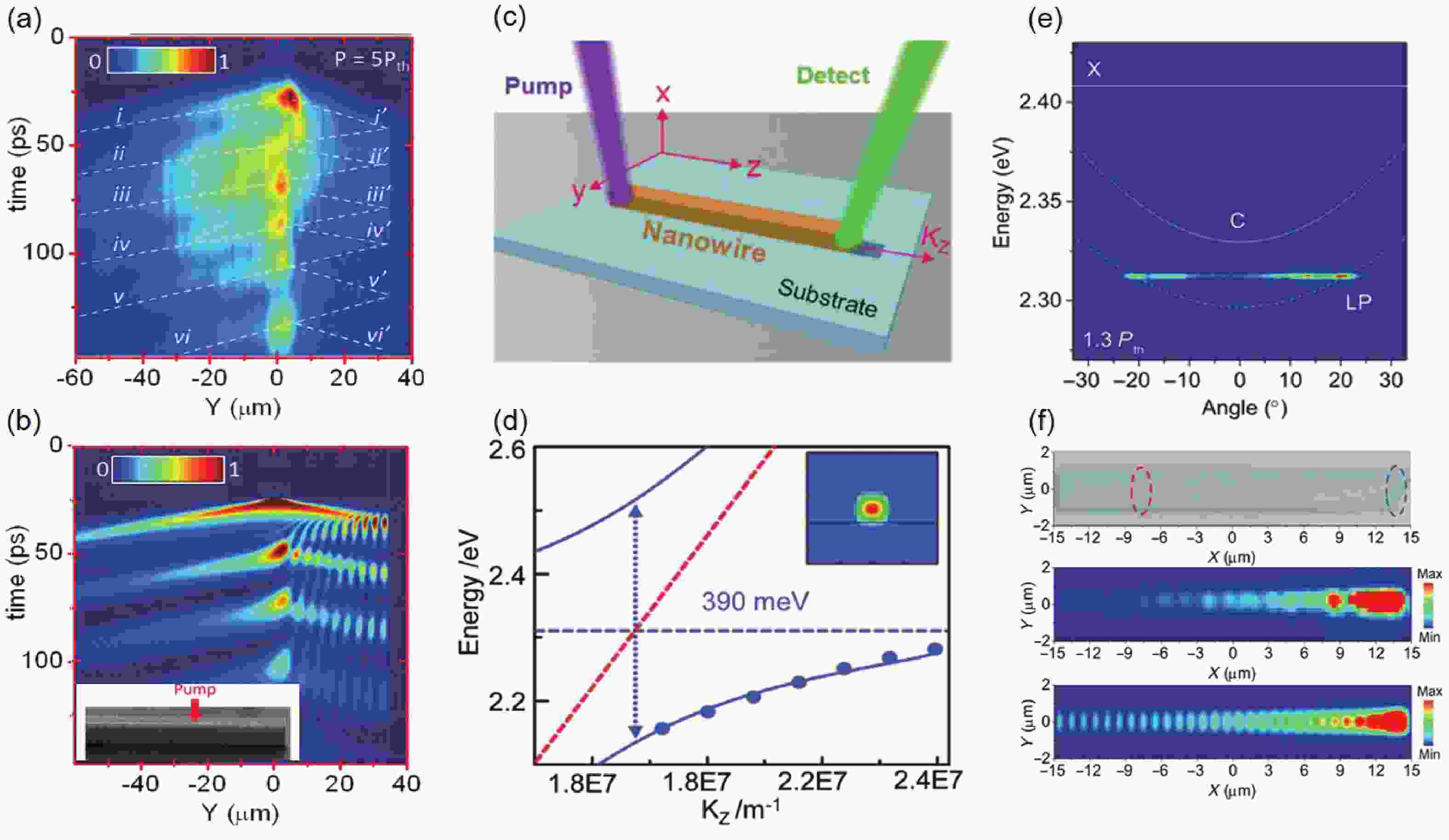
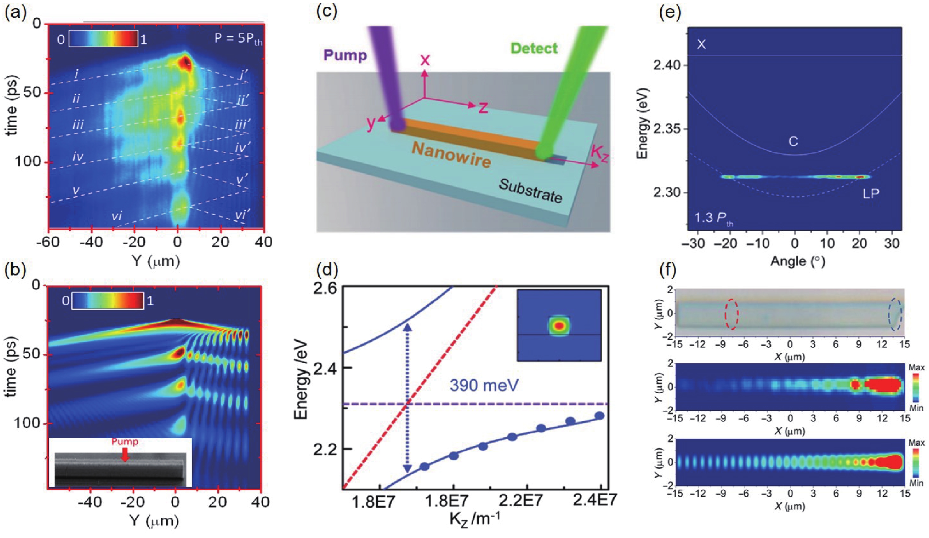
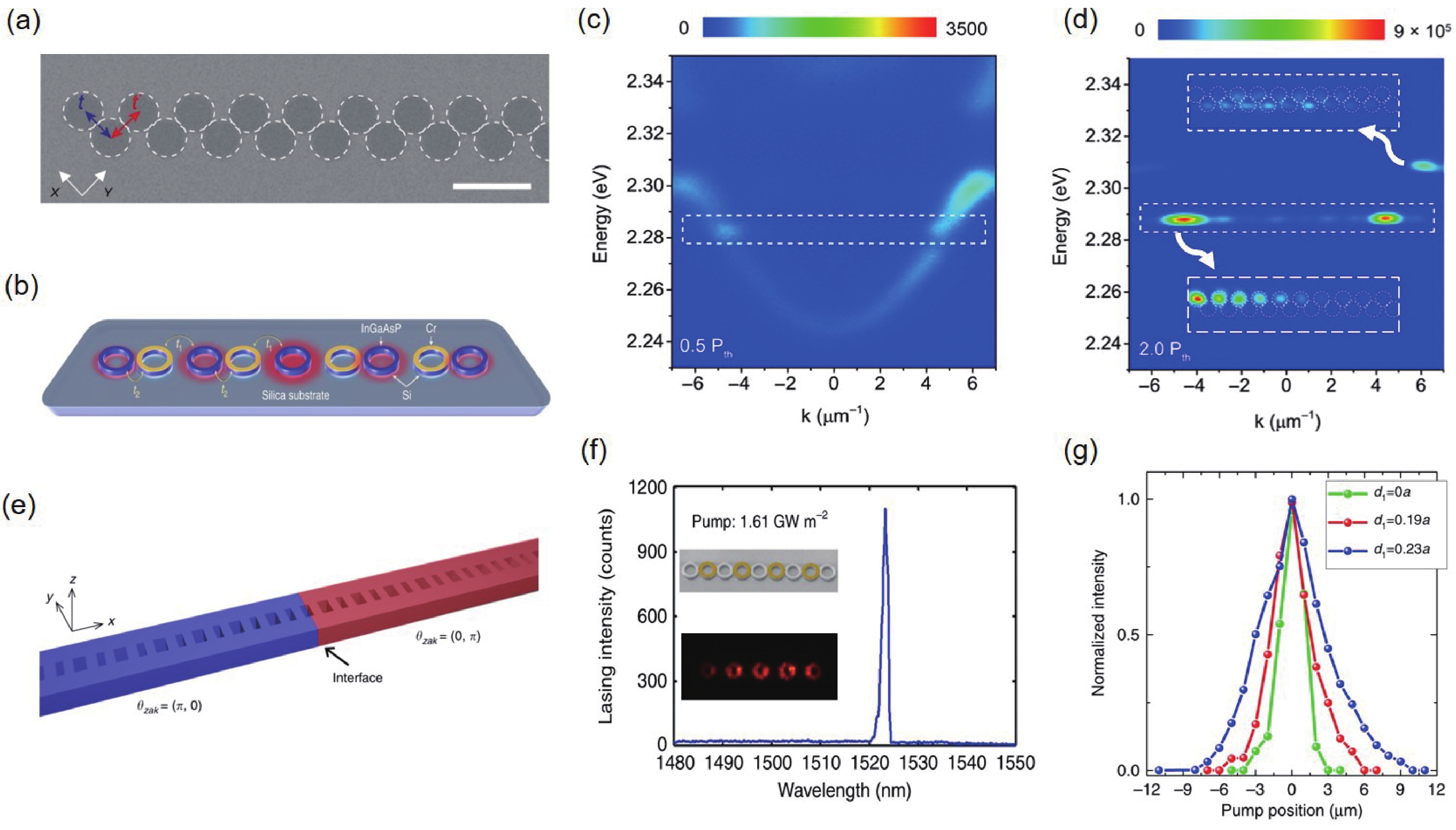
In recent years, one-dimensional (1D) nanomaterials have raised researcher's interest because of their unique structural characteristic to generate and confine the optical signal and their promising prospects in photonic applications. In this review, we summarized the recent research advances on the spectroscopy and carrier dynamics of 1D nanostructures. First, the condensation and propagation of exciton–polaritons in nanowires (NWs) are introduced. Second, we discussed the properties of 1D photonic crystal (PC) and applications in photonic–plasmonic structures. Third, the observation of topological edge states in 1D topological structures is introduced. Finally, the perspective on the potential opportunities and remaining challenges of 1D nanomaterials is proposed.


J. Semicond.
2022, 43(12): 122001 doi: 10.1088/1674-4926/43/12/122001

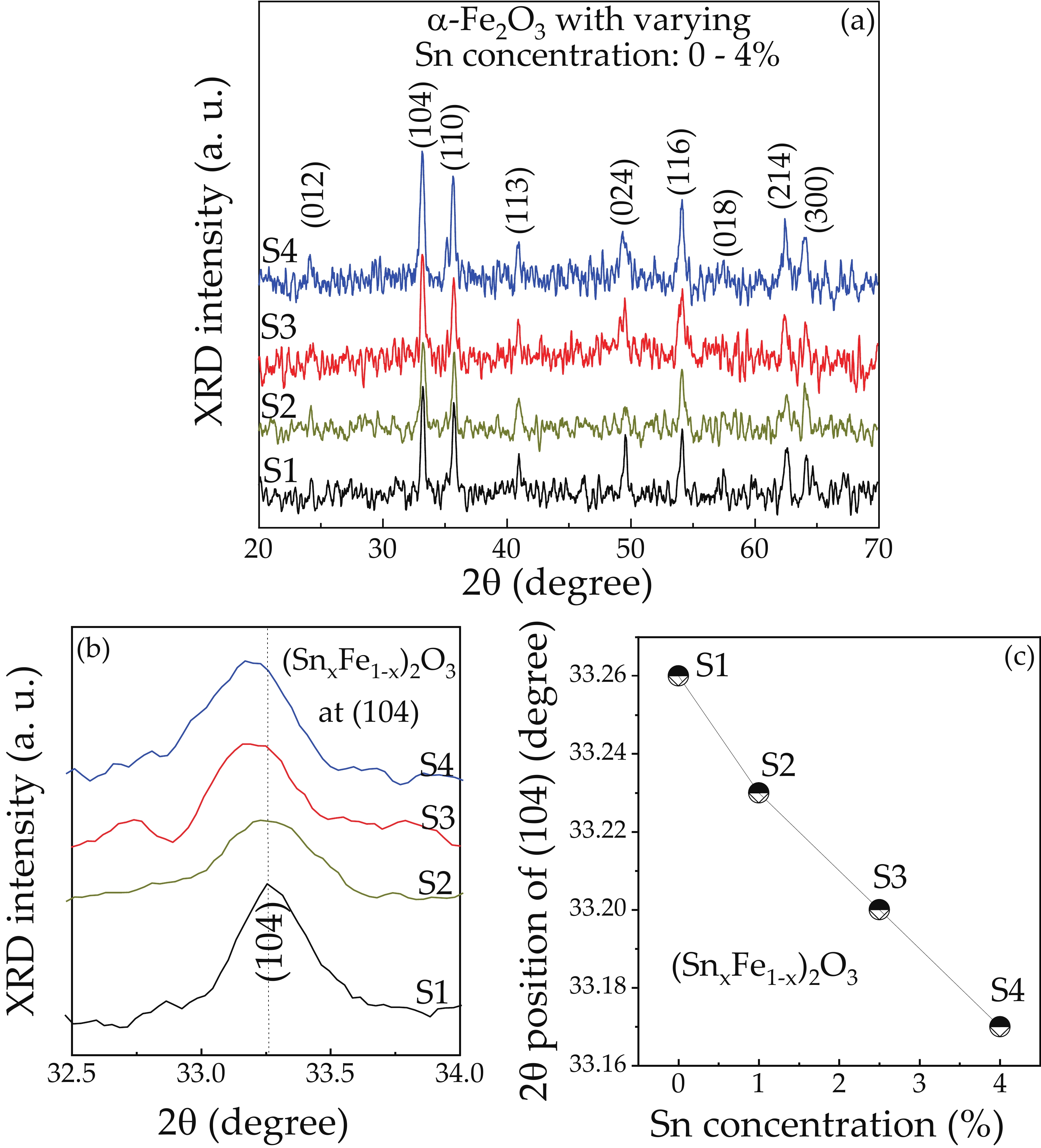
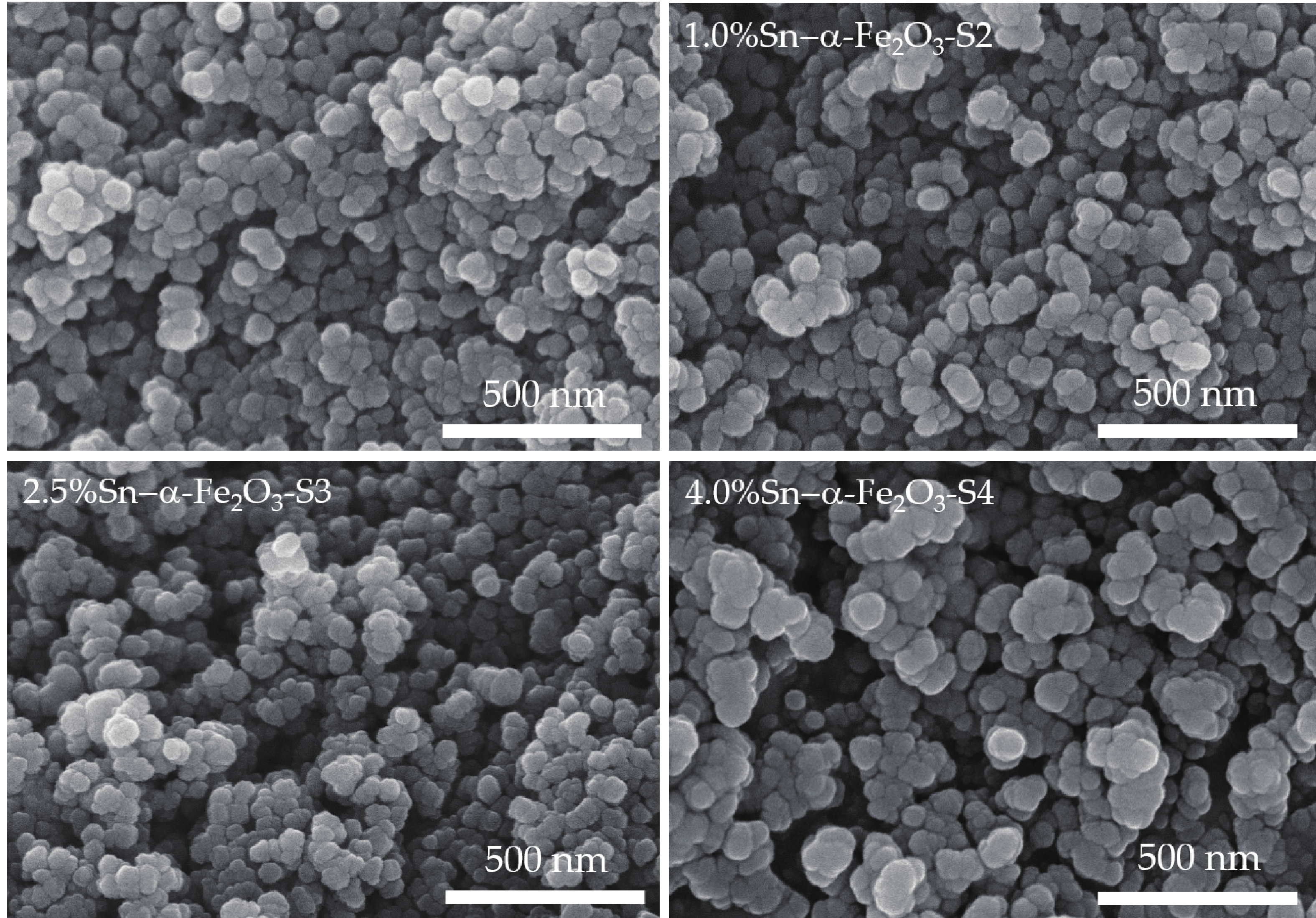
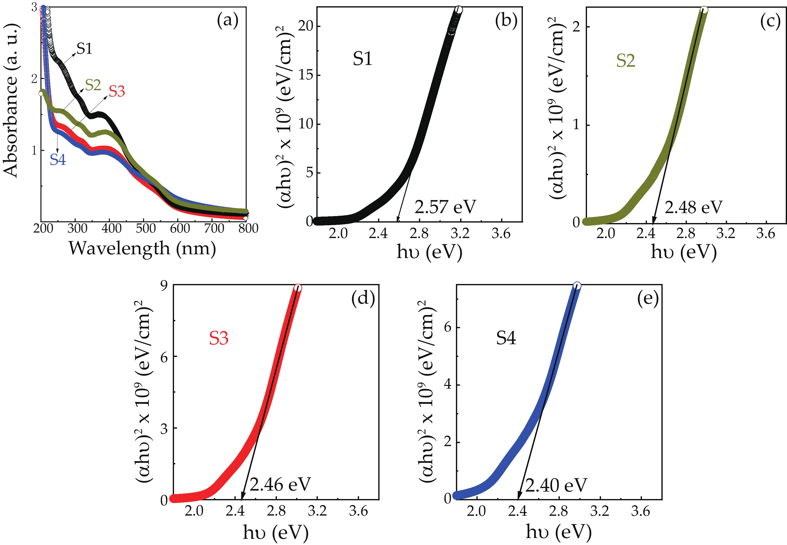
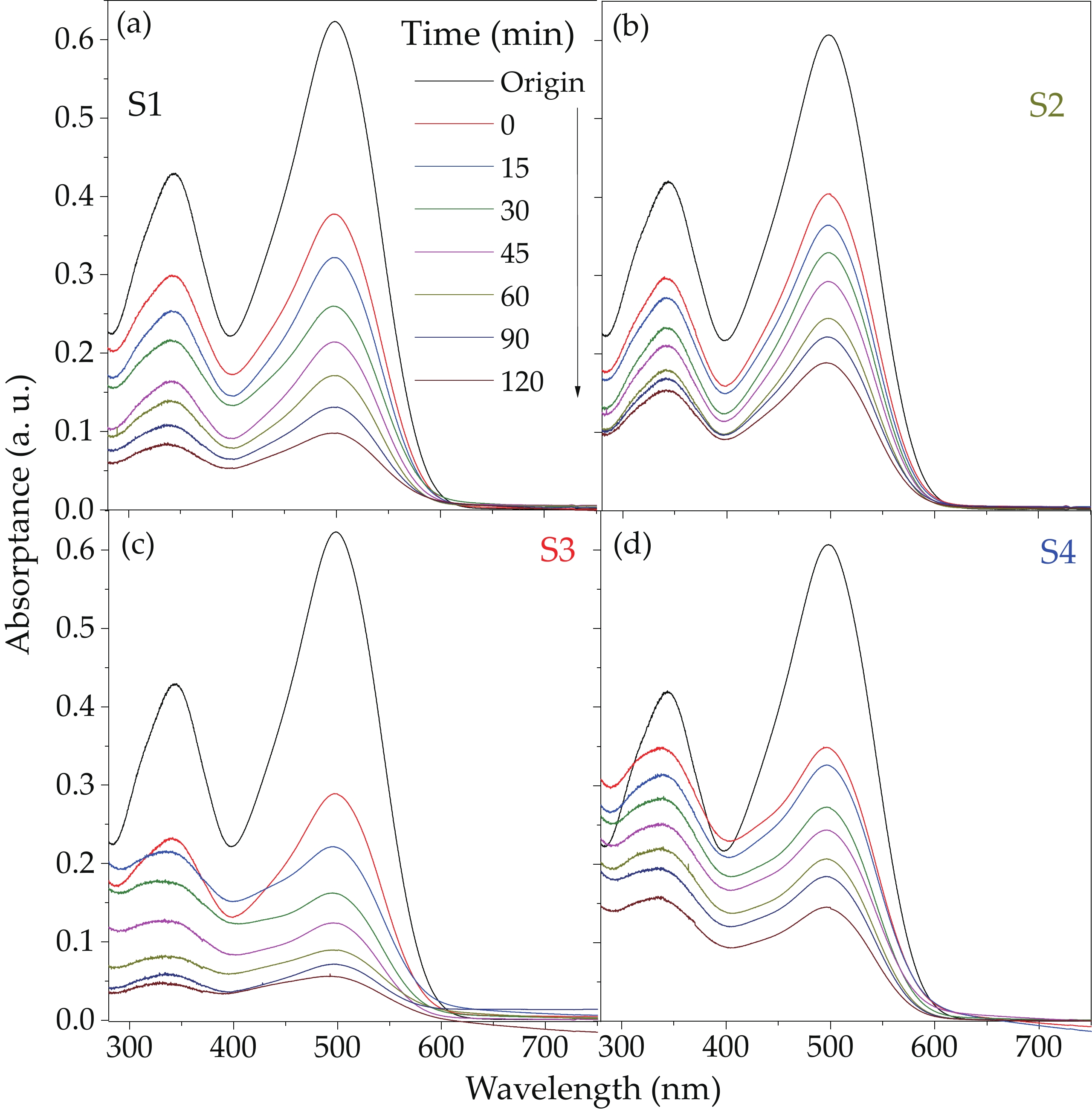
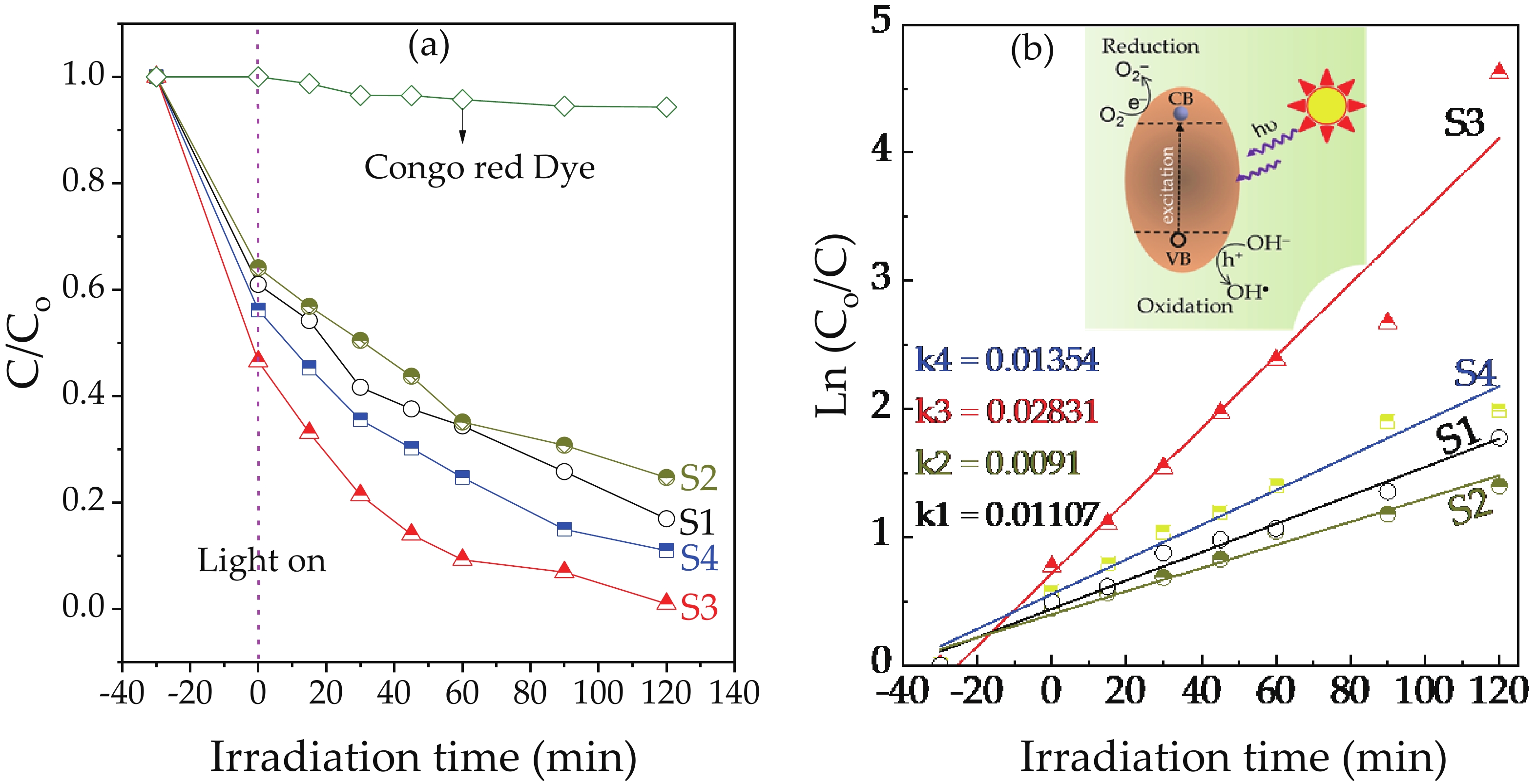
We report on the synthesis of Sn-doped hematite nanoparticles (Sn-α-Fe2O3 NPs) by the hydrothermal method. The prepared Sn-α-Fe2O3 NPs had a highly pure and well crystalline rhombohedral phase with an average particle size of 41.4 nm. The optical properties of as-synthesized α-Fe2O3 NPs show a higher bandgap energy (2.40–2.57 eV) than that of pure bulk α-Fe2O3 (2.1 eV). By doping Sn into α-Fe2O3 NPs, the Sn-doped hematite was observed a redshift toward a long wavelength with increasing Sn concentration from 0% to 4.0%. The photocatalytic activity of Sn-doped α-Fe2O3 NPs was evaluated by Congo red (CR) dye degradation. The degradation efficiency of CR dye using Sn-α-Fe2O3 NPs catalyst is higher than that of pure α-Fe2O3 NPs. The highest degradation efficiency of CR dye was 97.8% using 2.5% Sn-doped α-Fe2O3 NPs catalyst under visible-light irradiation. These results suggest that the synthesized Sn-doped α-Fe2O3 nanoparticles might be a suitable approach to develop a photocatalytic degradation of toxic inorganic dye in wastewater.

J. Semicond.
2022, 43(12): 122101 doi: 10.1088/1674-4926/43/12/122101
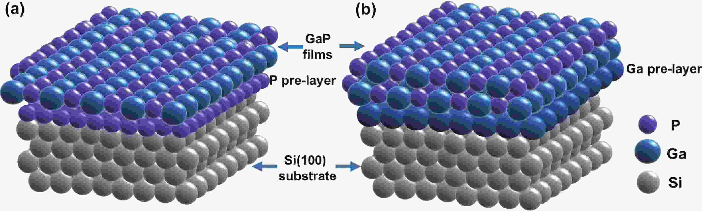
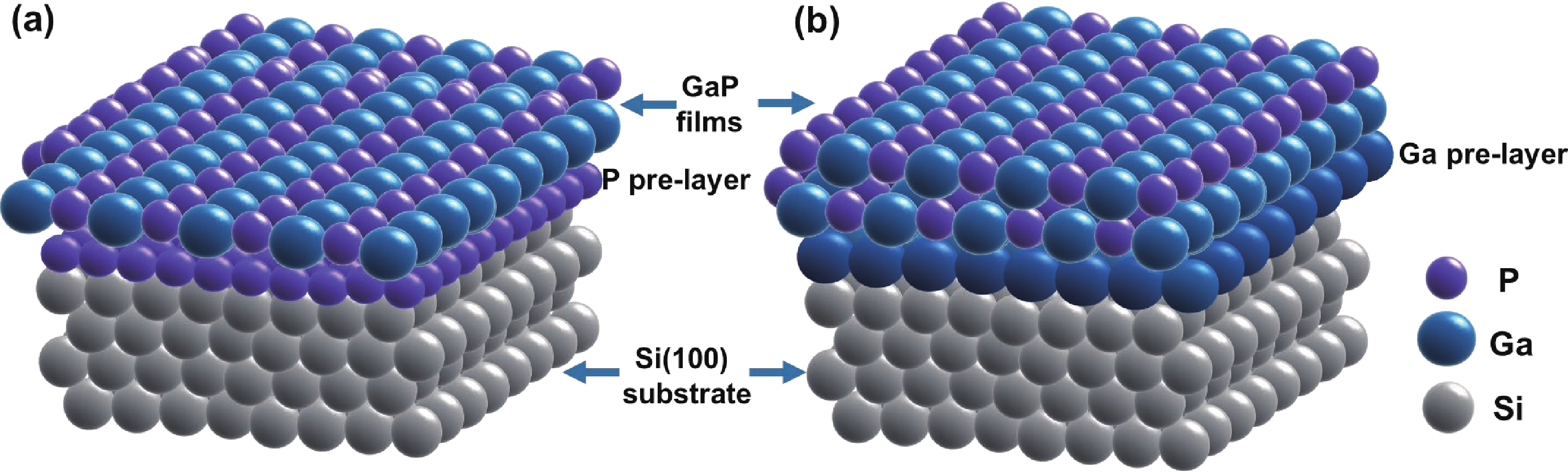
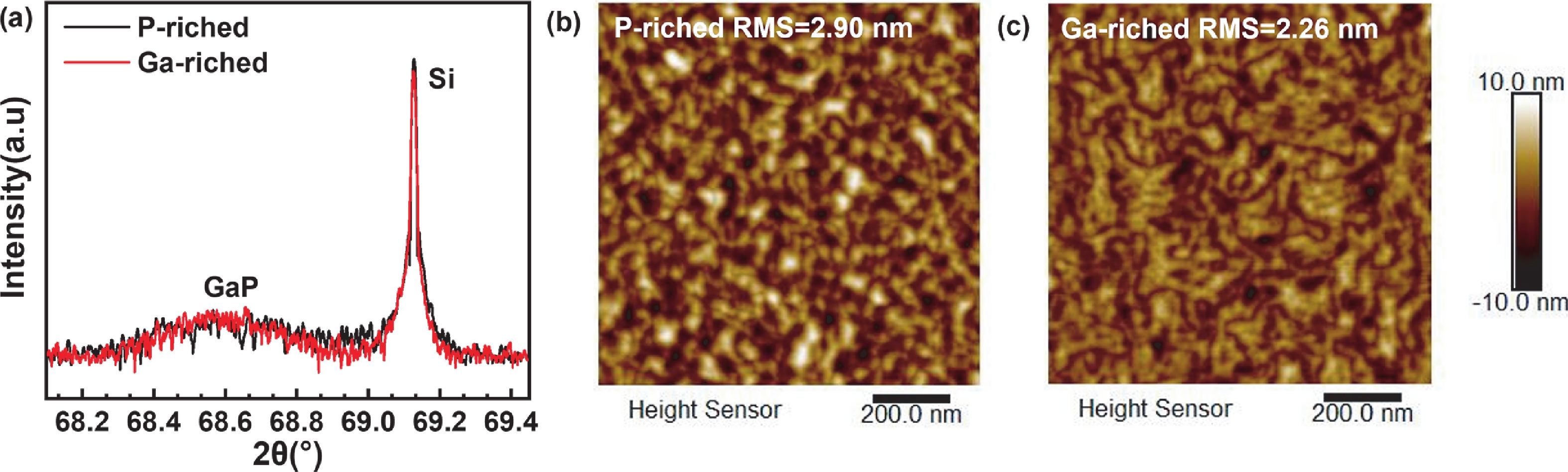
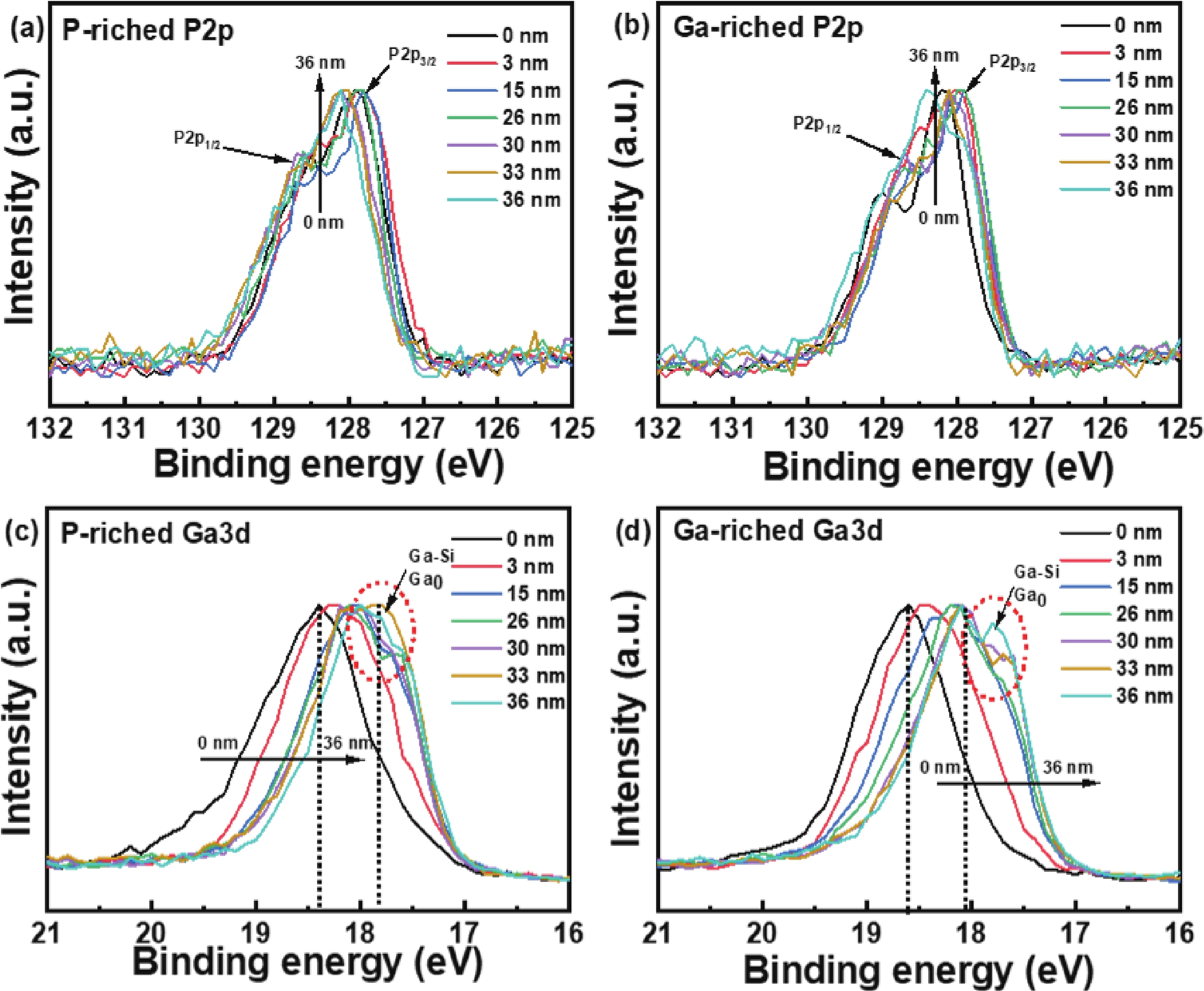
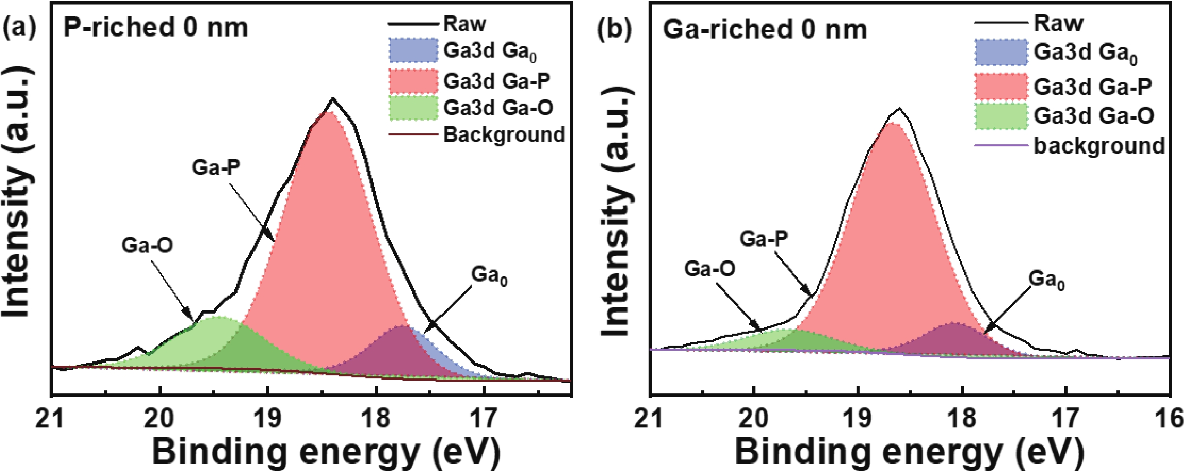
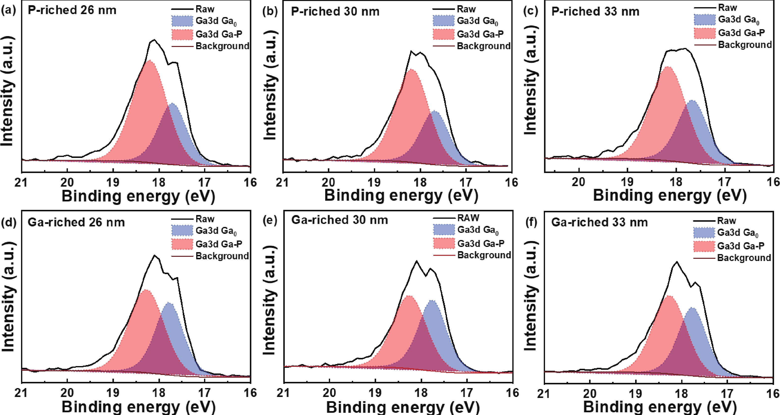
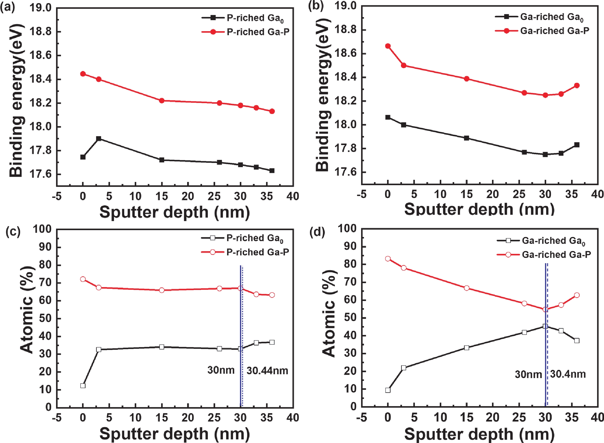
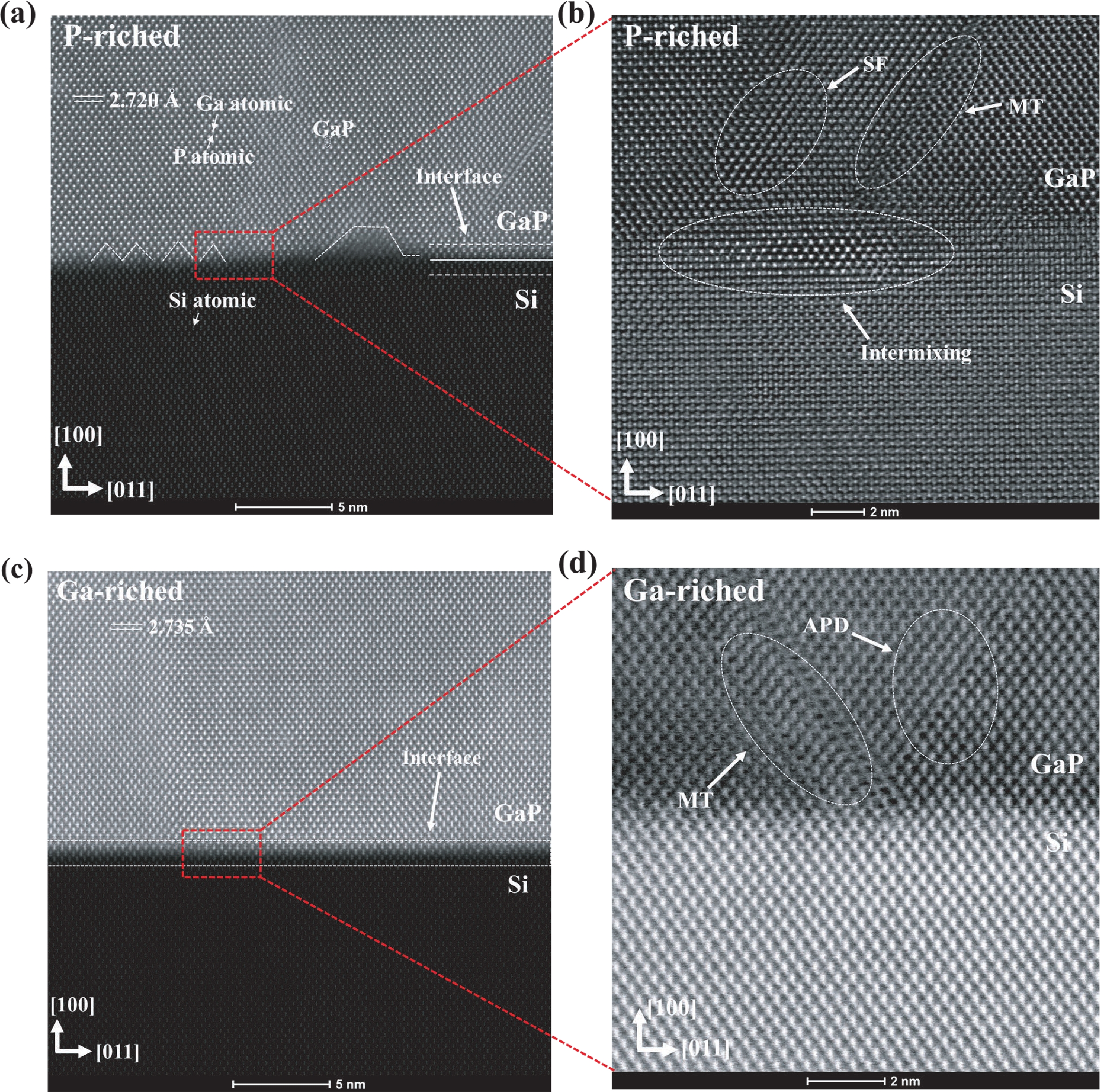
The atomic structure and surface chemistry of GaP/Si(100) heterostructure with different pre-layers grown by molecular beam epitaxy are studied. It is found that GaP epilayer with Ga-riched pre-layers on Si(100) substrate has regular surface morphology and stoichiometric abrupt heterointerfaces from atomic force microscopes (AFMs) and spherical aberration-corrected transmission electron microscopes (ACTEMs). The interfacial dynamics of GaP/Si(100) heterostructure is investigated by X-ray photoelectron spectroscopy (XPS) equipped with an Ar gas cluster ion beam, indicating that Ga pre-layers can lower the interface formation energy and the bond that is formed is more stable. These results suggest that Ga-riched pre-layers are more conducive to the GaP nucleation as well as the epitaxial growth of GaP material on Si(100) substrate.
J. Semicond.
2022, 43(12): 122102 doi: 10.1088/1674-4926/43/12/122102
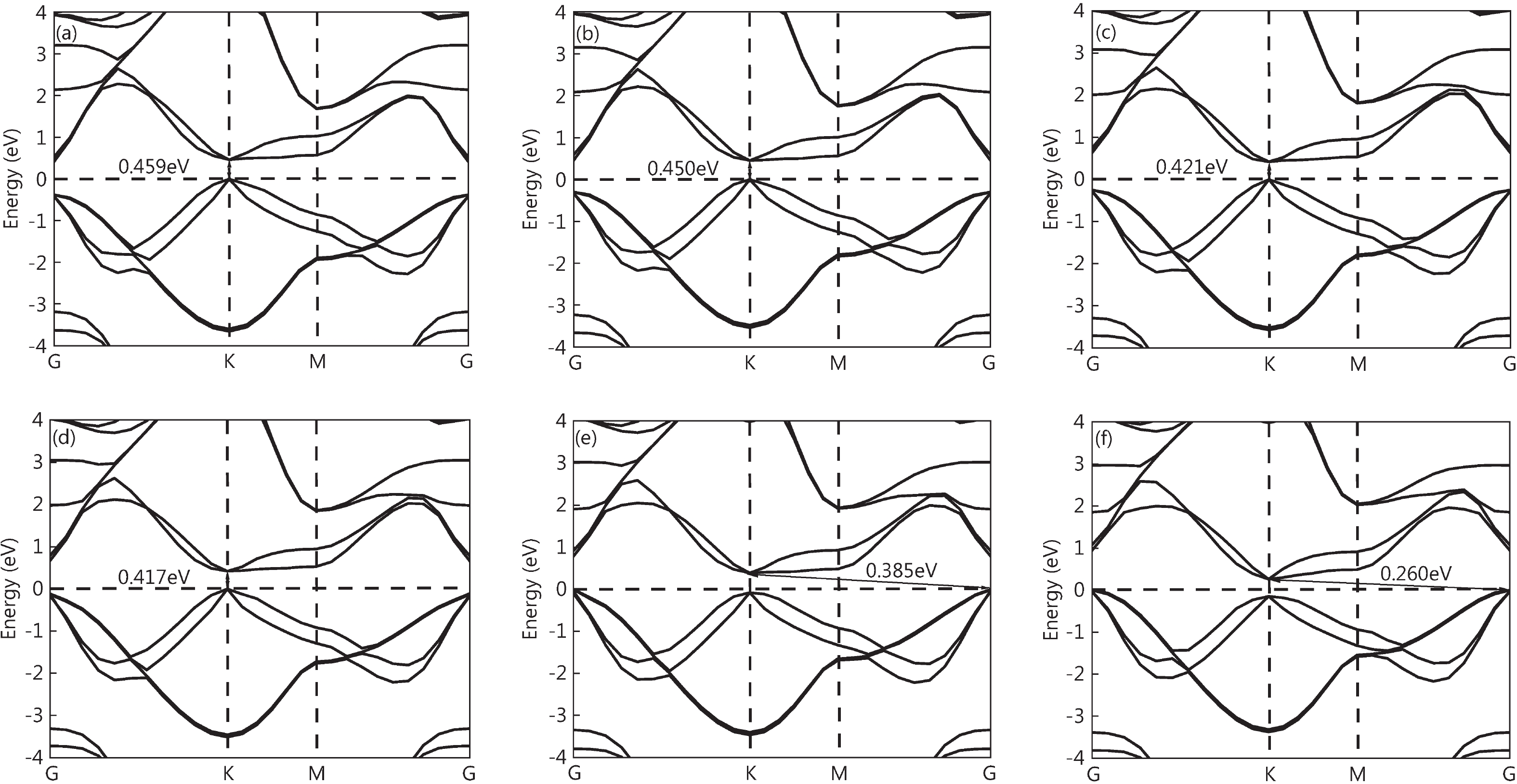
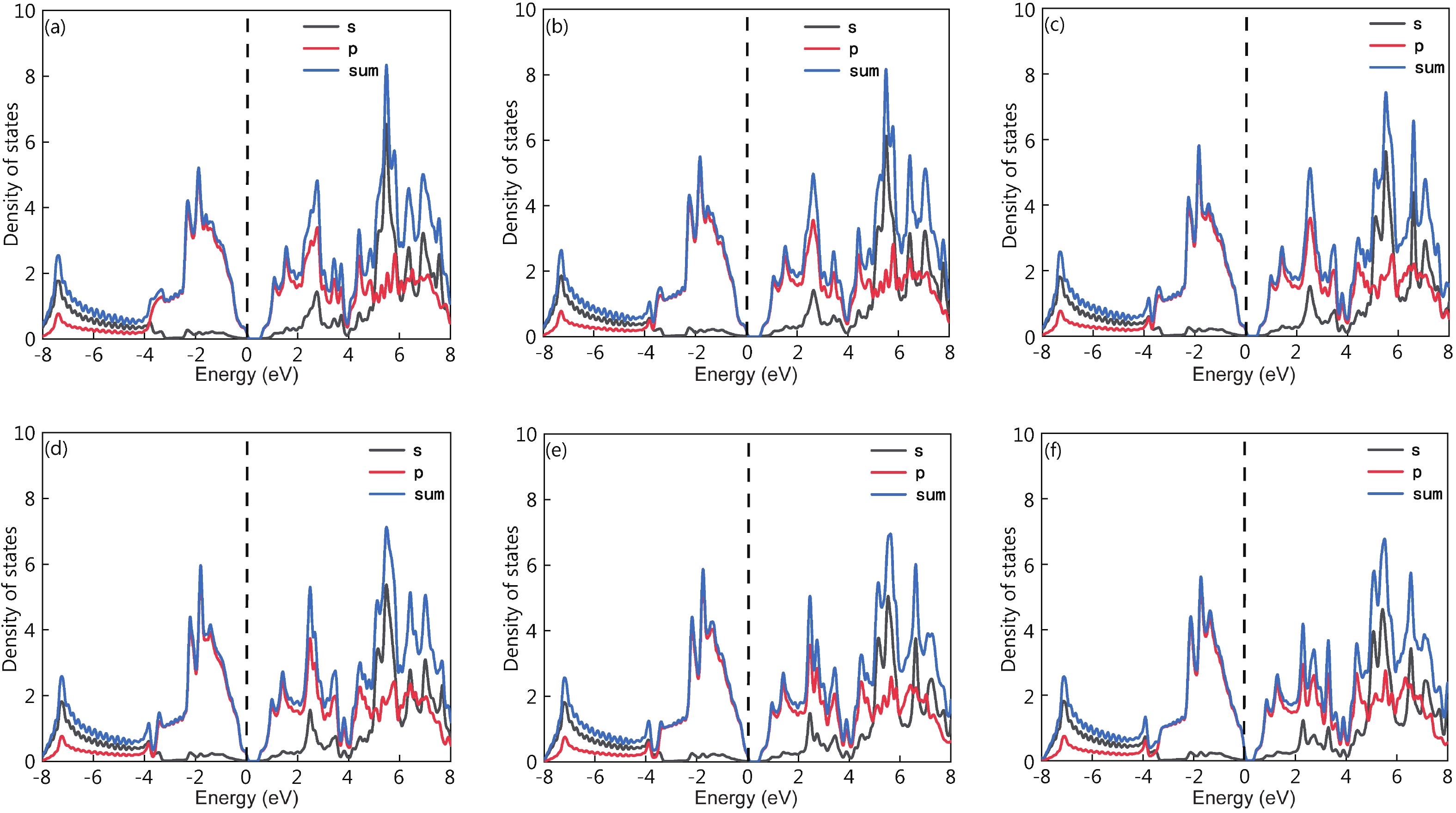
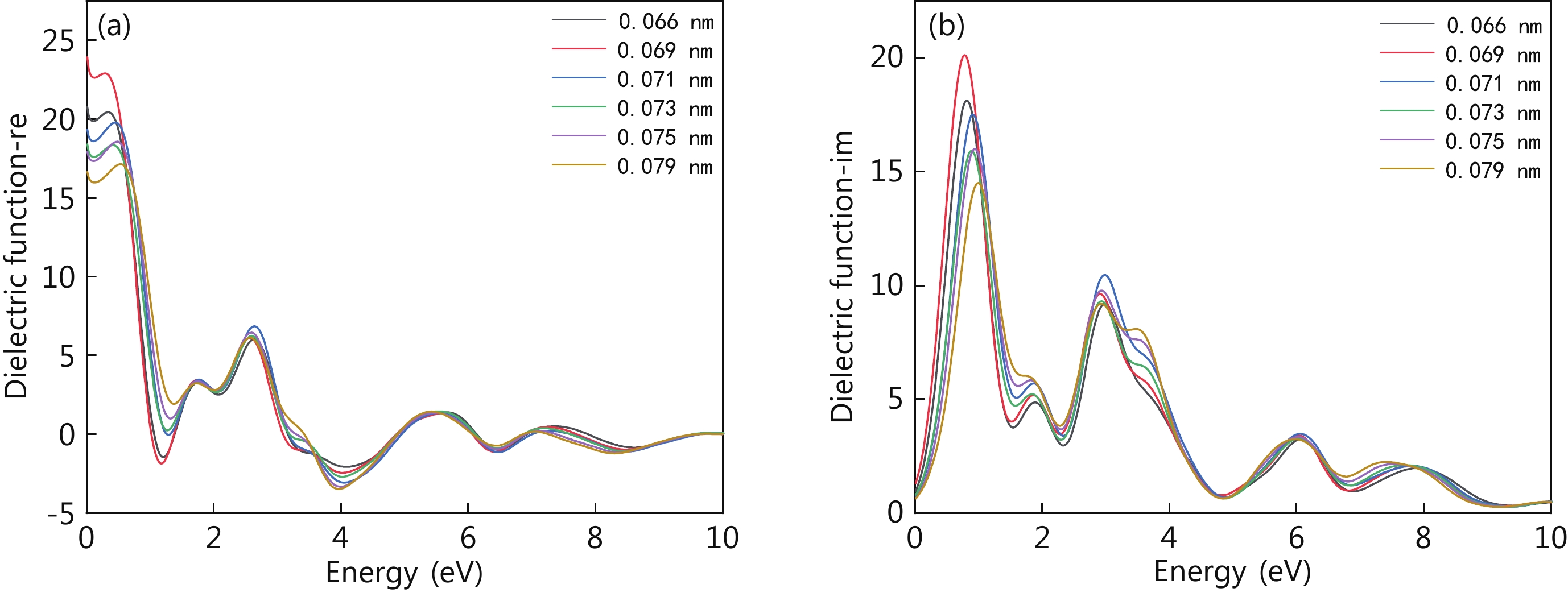
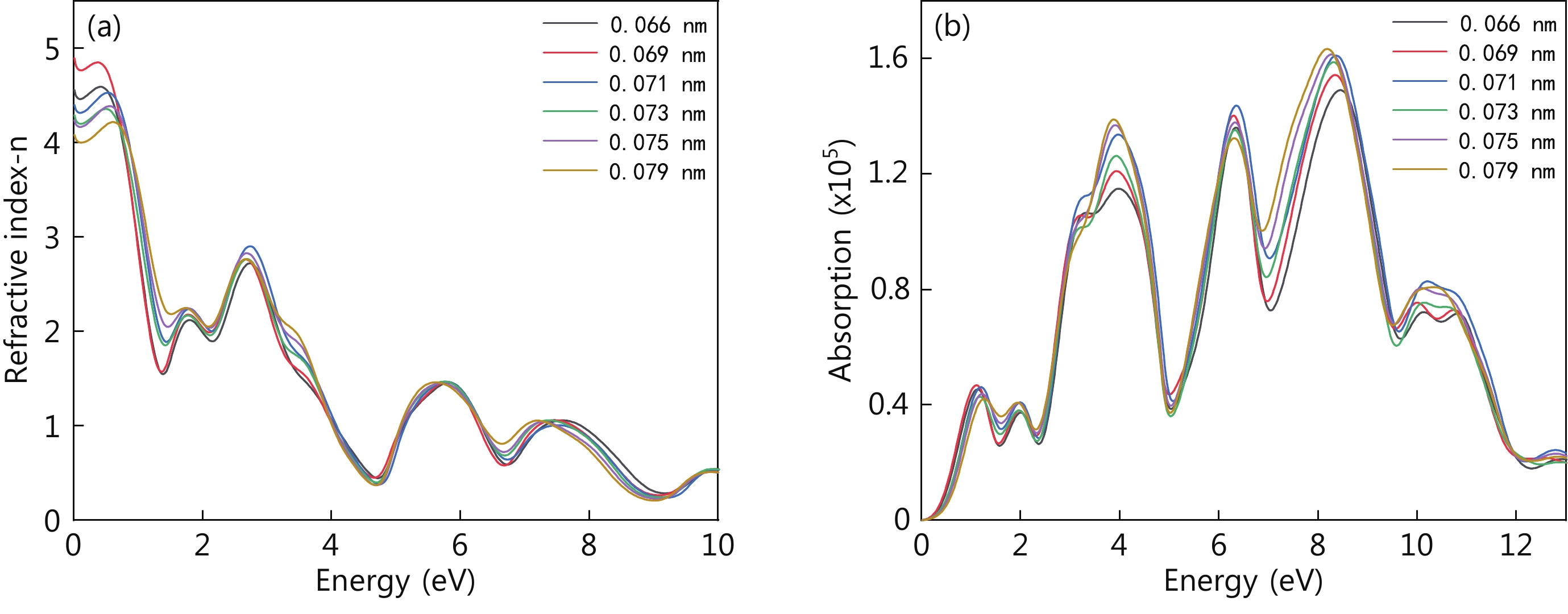
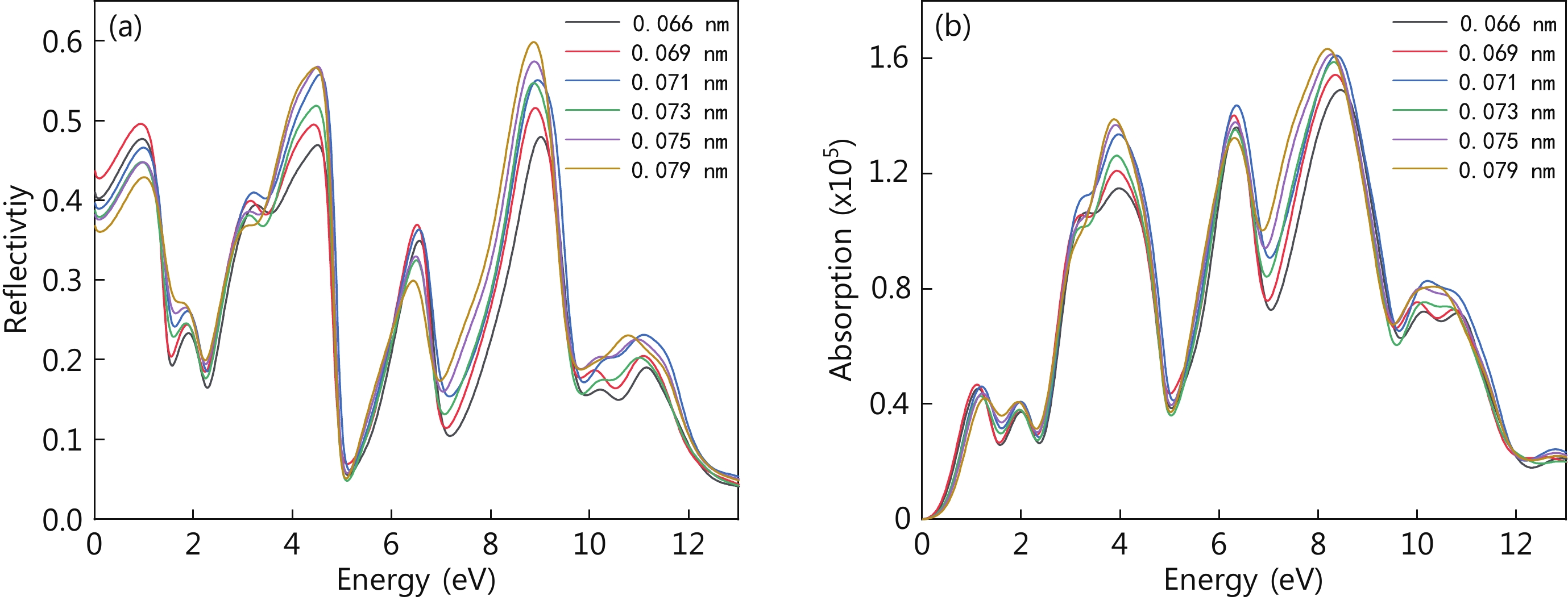
The electronic structure and optical properties of bilayer germanene under different warpages are studied by the first-principles method of density functional theory. The effects of warpages on the electronic structure and optical properties of bilayer germanene are analyzed. The results of the electronic structure study show that the bottom of the conduction band of bilayer germanene moves to the lower energy direction with the increase of warpages at the K point, and the top of the valence band stays constant at the K point, and so the band gap decreases with the increase of warpage. When the warpage is 0.075 nm, the top of the valence band of bilayer germanene changes from K point to G point, and the bilayer germanene becomes an indirect band gap semiconductor. This is an effective means to modulate the conversion of bilayer germanene between direct band gap semiconductor and indirect band gap semiconductor by adjusting the band structure of bilayer germanene effectively. The study of optical properties shows that the effect of warpage on the optical properties of bilayer germanene is mainly distributed in the ultraviolet and visible regions, and the warpage can effectively regulate the electronic structure and optical properties of bilayer germanene. When the warpage is 0.069 nm, the first peak of dielectric function and extinction coefficient is the largest, and the energy corresponding to the absorption band edge is the smallest. Therefore, the electron utilization rate is the best when the warpage is 0.069 nm.

J. Semicond.
2022, 43(12): 122301 doi: 10.1088/1674-4926/43/12/122301
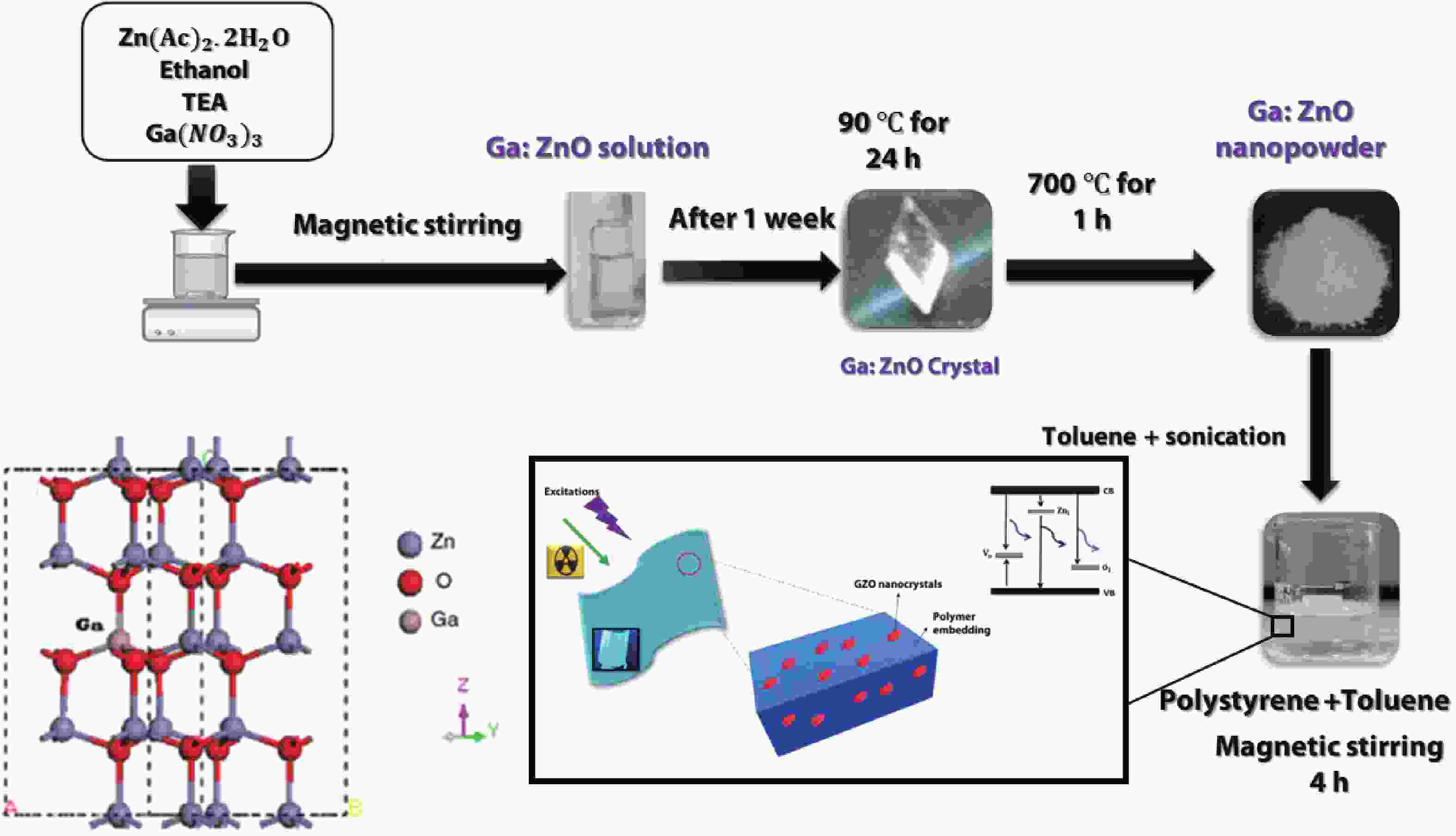
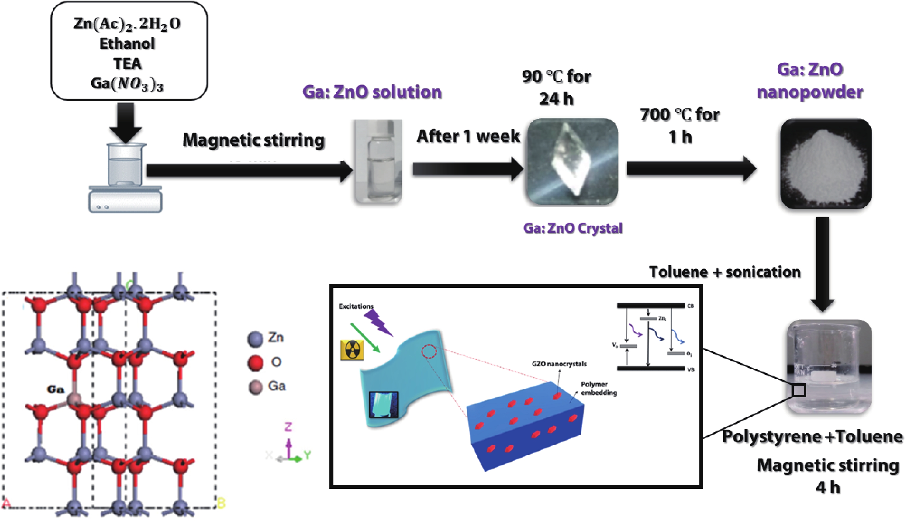
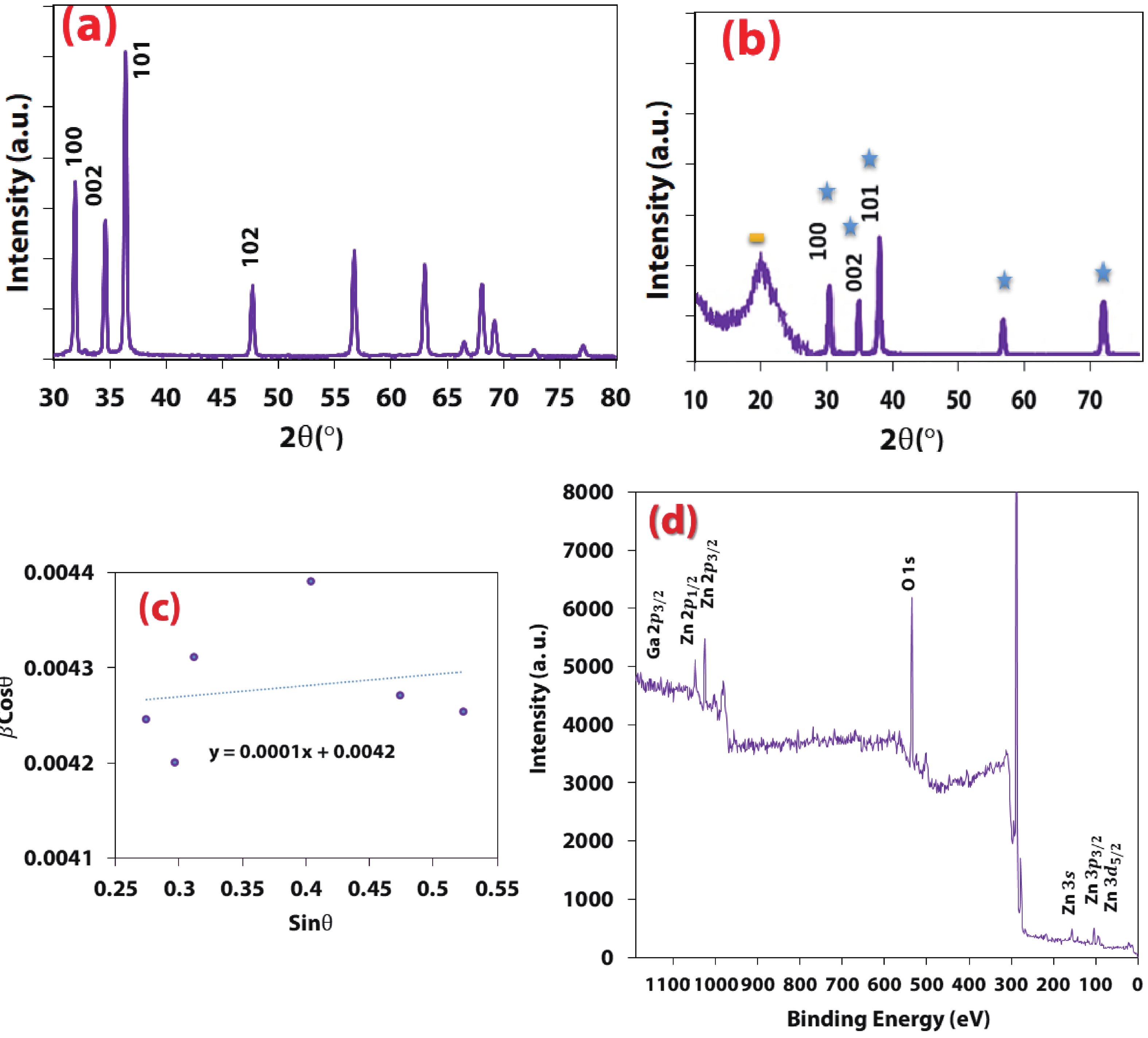
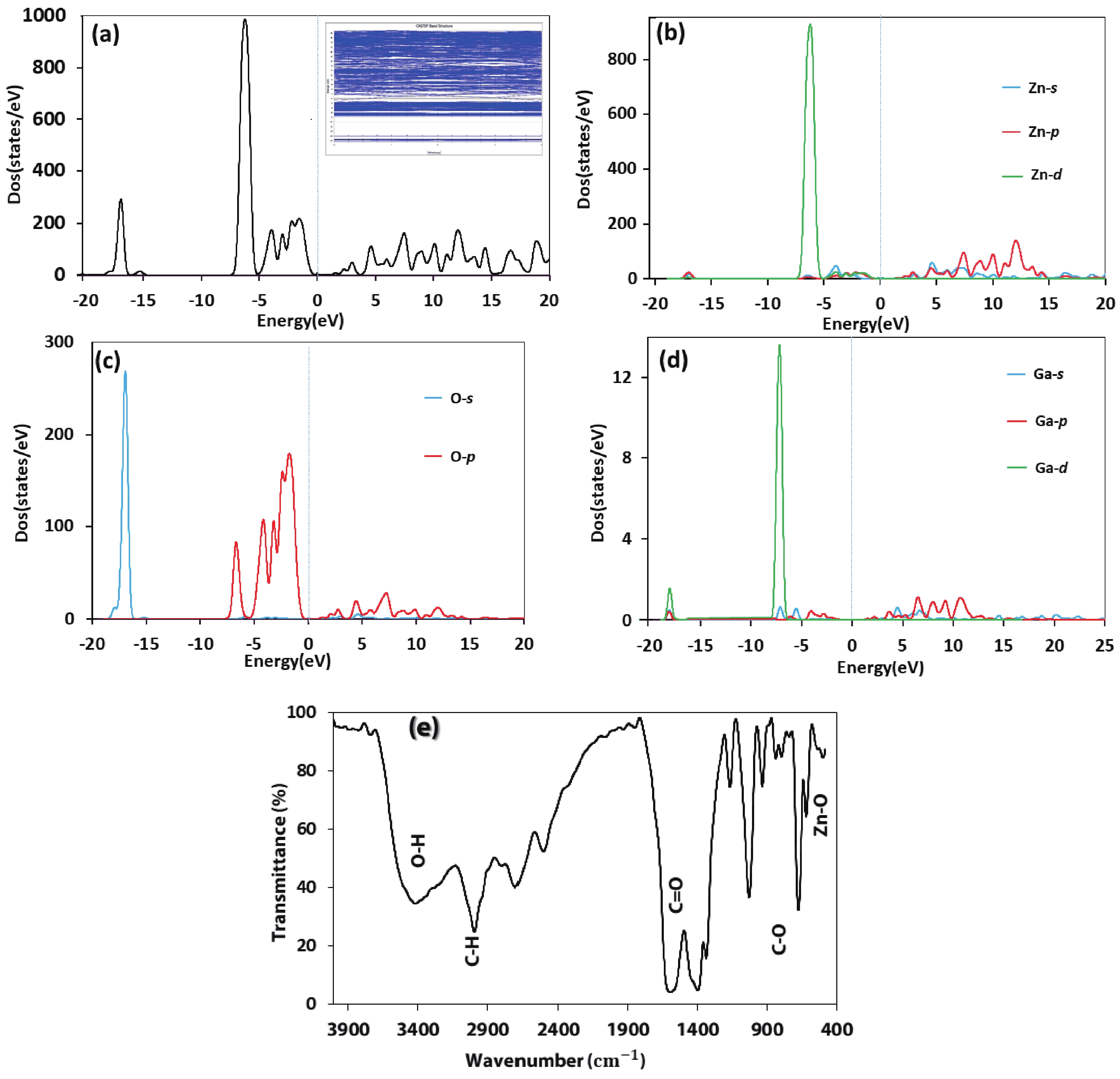
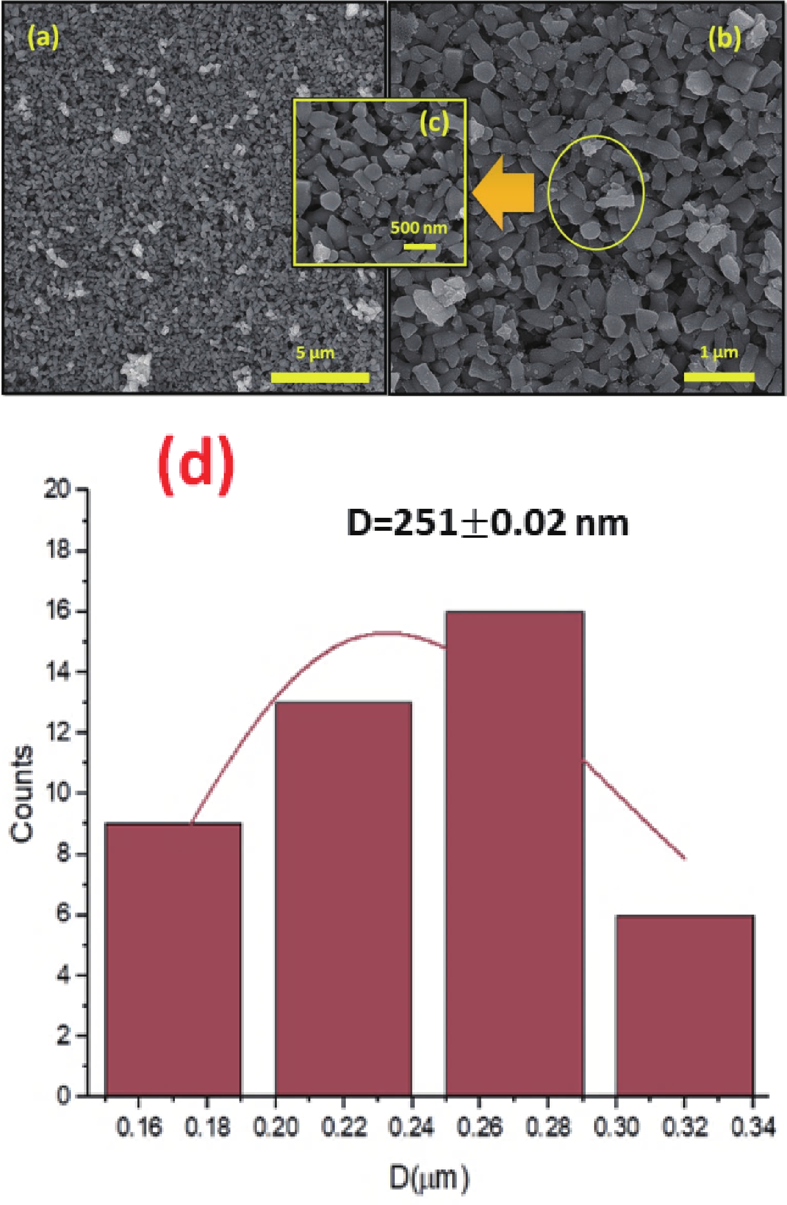
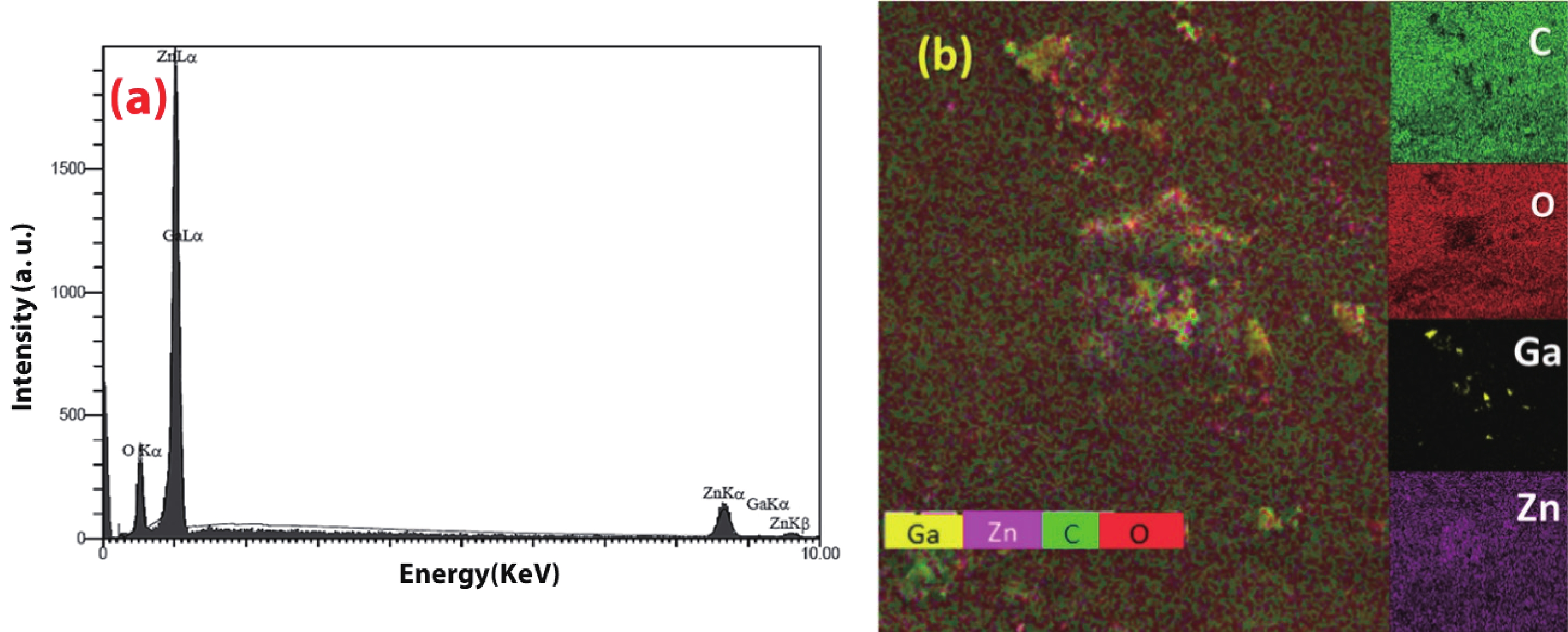
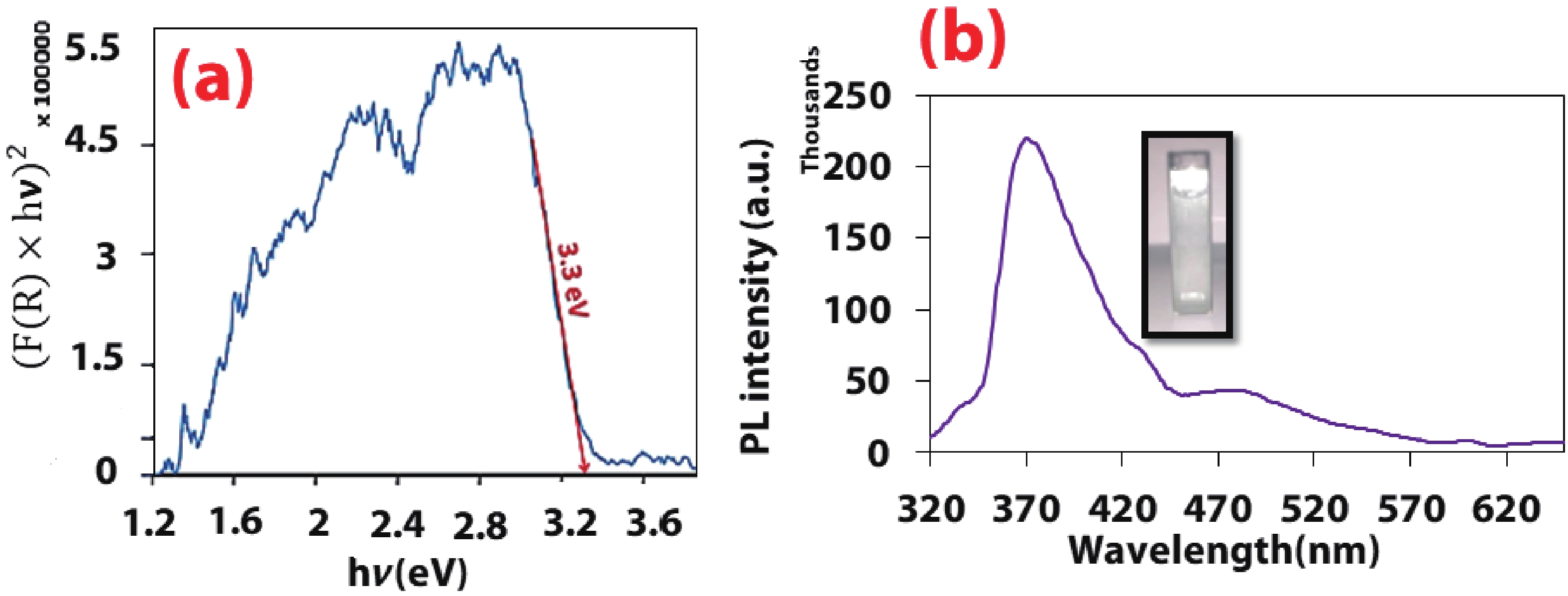
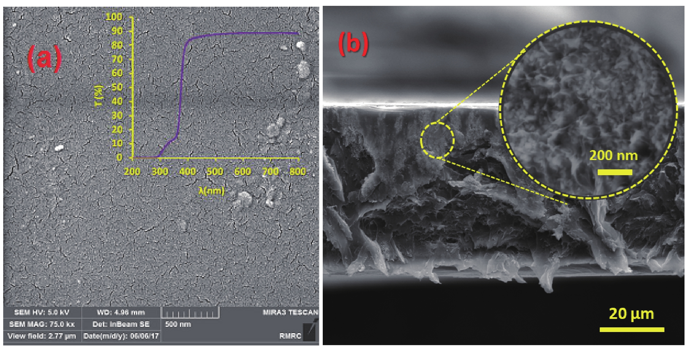
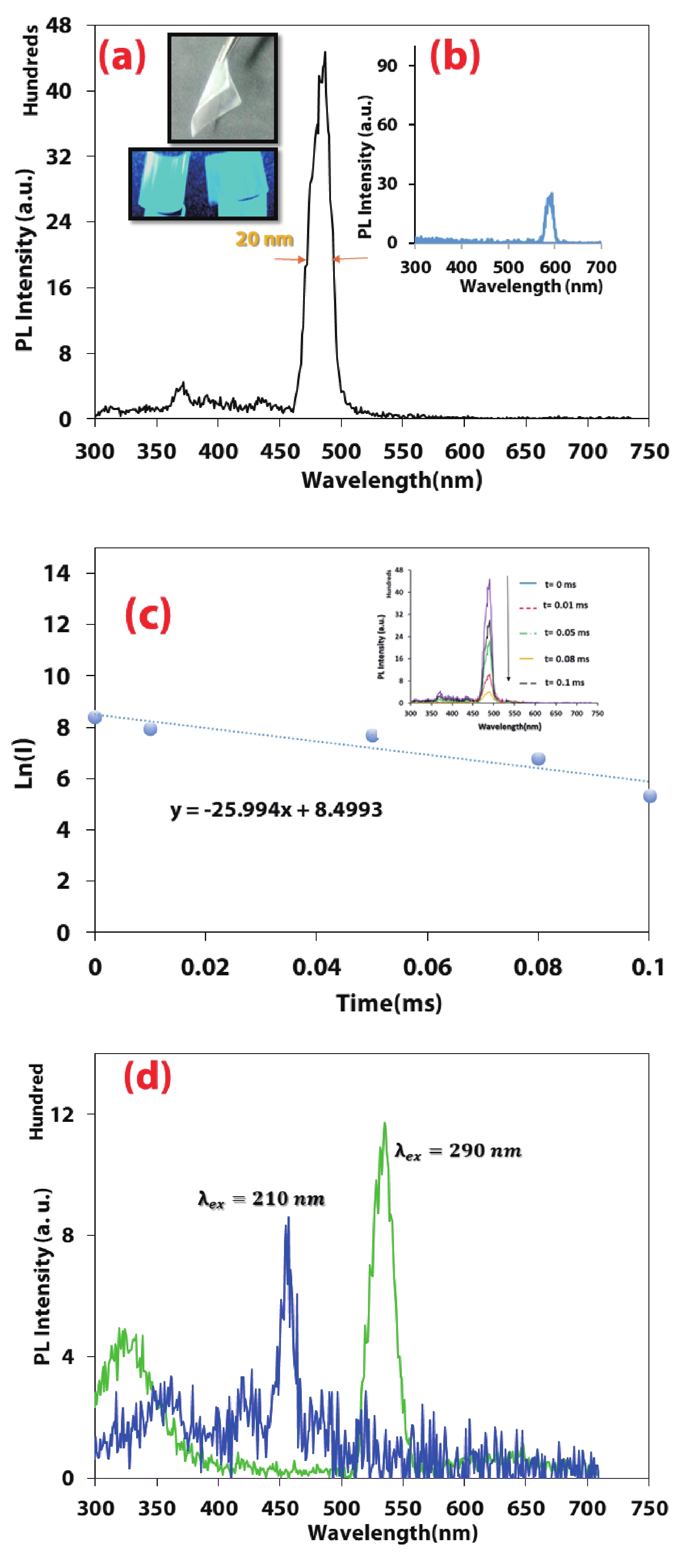
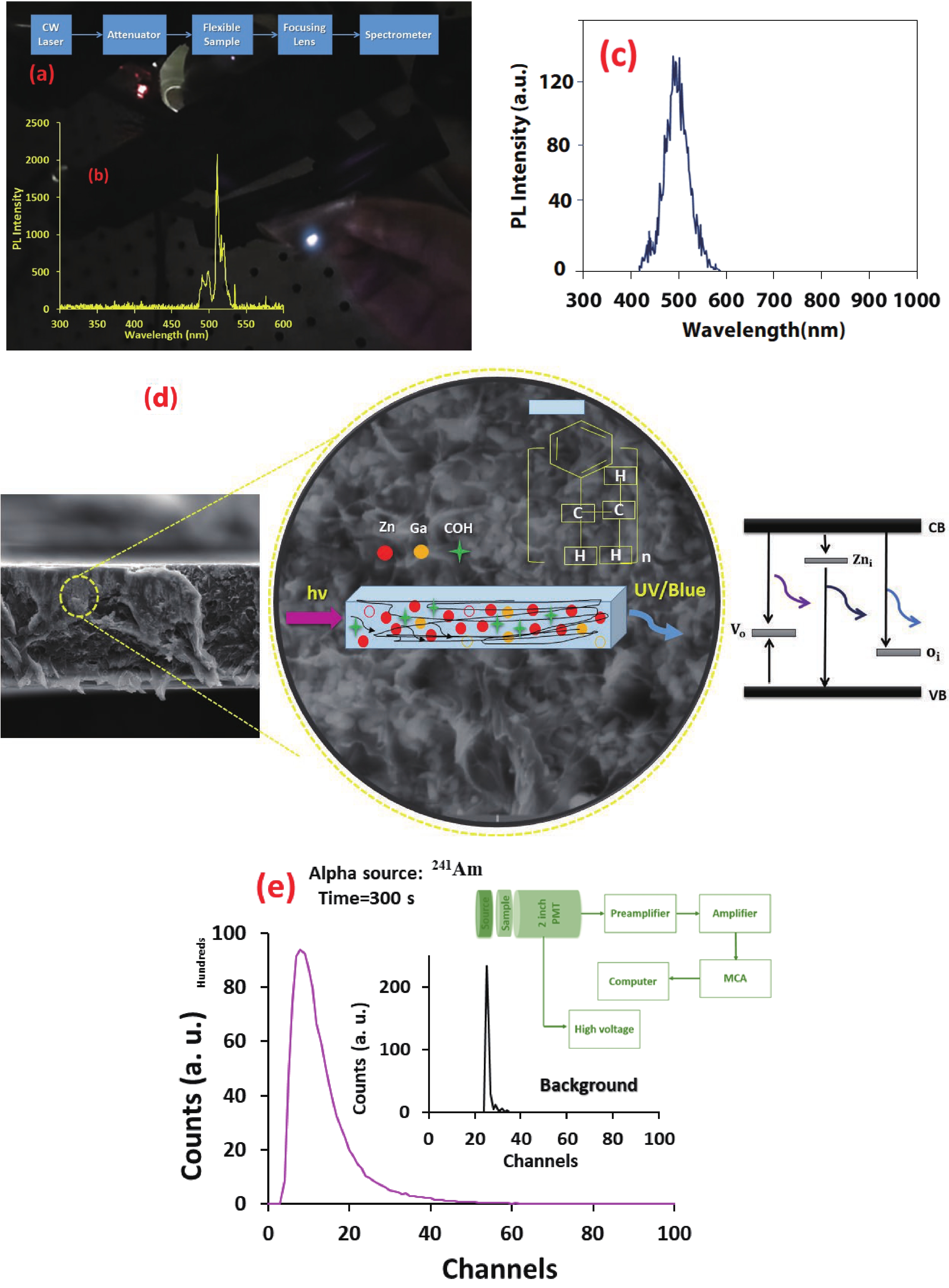
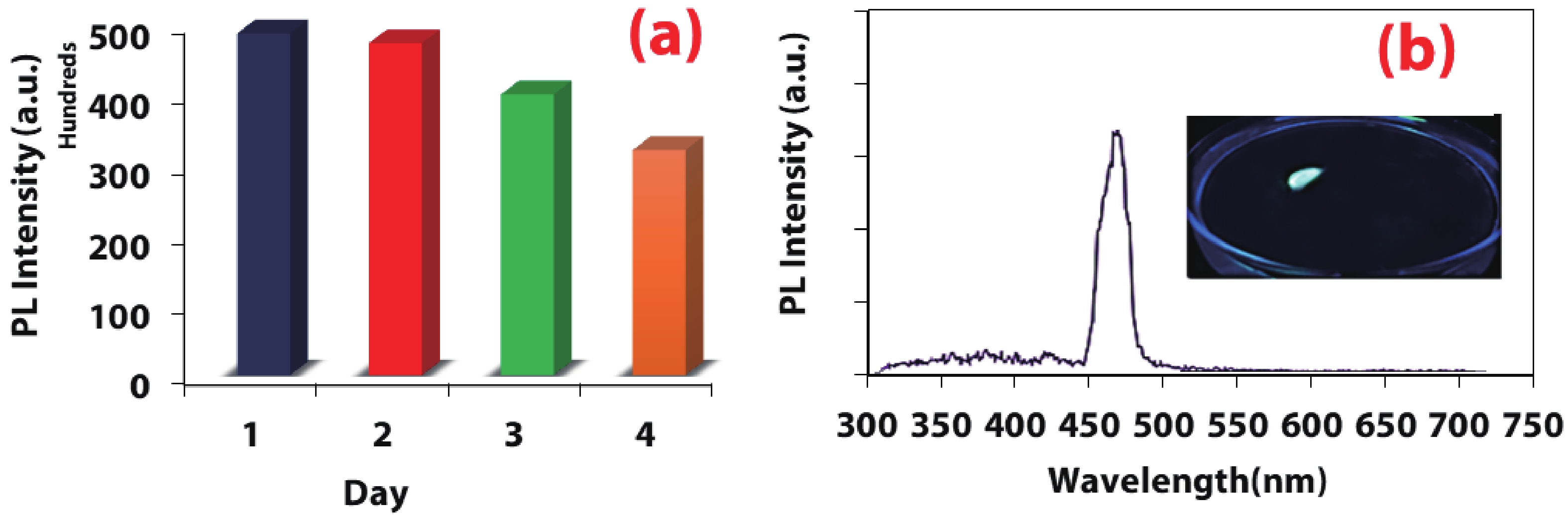
In the present study, a simple method for the preparation of a luminescent flexible gallium doped zinc oxide (GZO)/polystyrene nanocomposite film was developed. The prepared GZO powder was characterized through different optical and structural techniques. The XRD study revealed the existence of a wurtzite structure with no extra oxide peaks. Elemental-mapping, EDX, FTIR and XPS analyses were used to confirm the presence of elements and the several groups present in the structure. Under excitations of UV, the prepared hybrid nanocomposite showed a strong cyan emission with narrow full width at half the maximum value (20 nm) that has not been reported before. X-ray and laser-induced luminescence results of the hybrid film revealed novel blue-green emission at room temperature. The prepared composite film showed a strong scintillation response to ionizing radiation. The strong emissions, very weak deep-level emissions, and low FWHM of composite indicate the desirable optical properties with low-density structural defects in the GZO composite structure. Therefore, the prepared hybrid film can be considered to be a suitable candidate for the fabrication of optoelectronic devices.
J. Semicond.
2022, 43(12): 122401 doi: 10.1088/1674-4926/43/12/122401

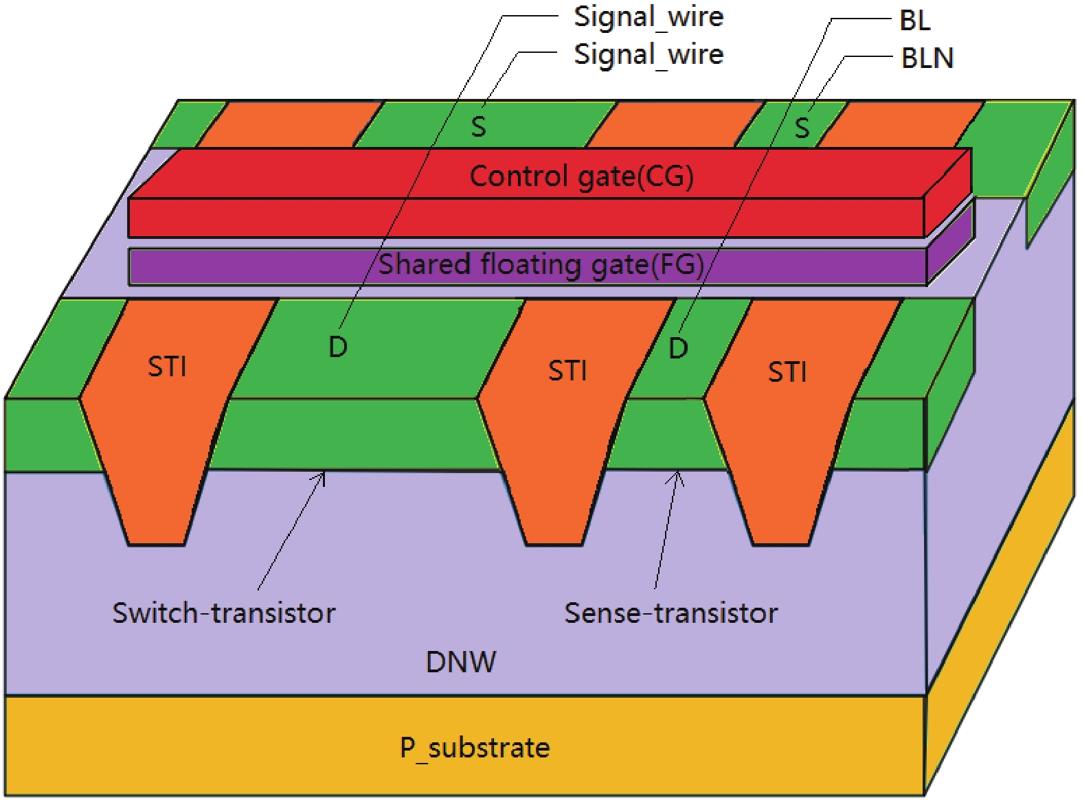
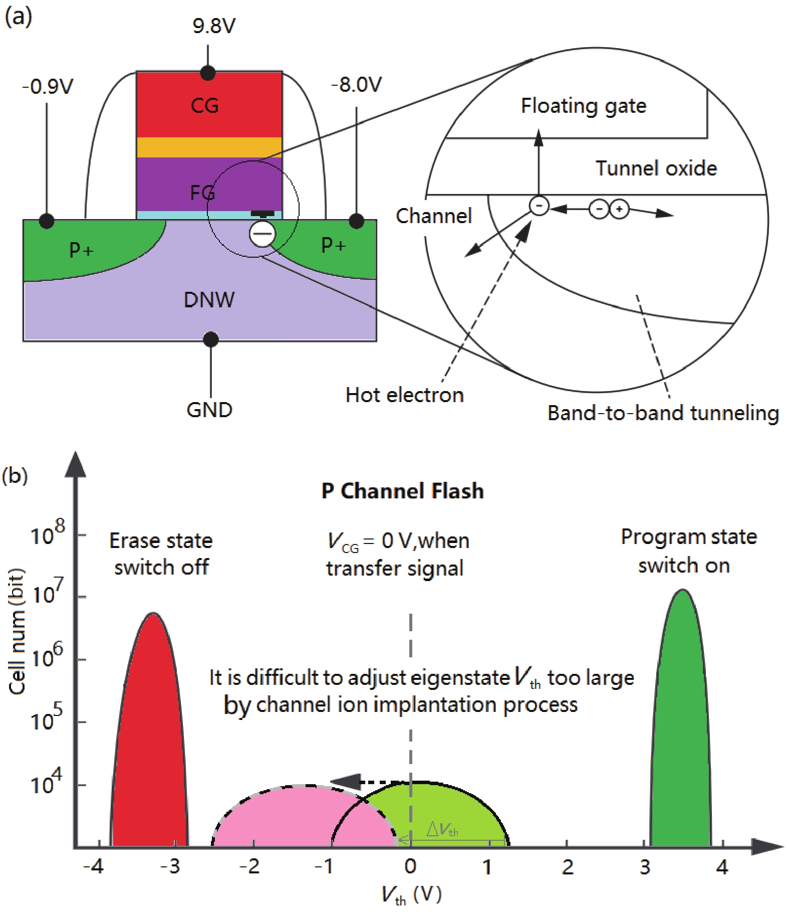
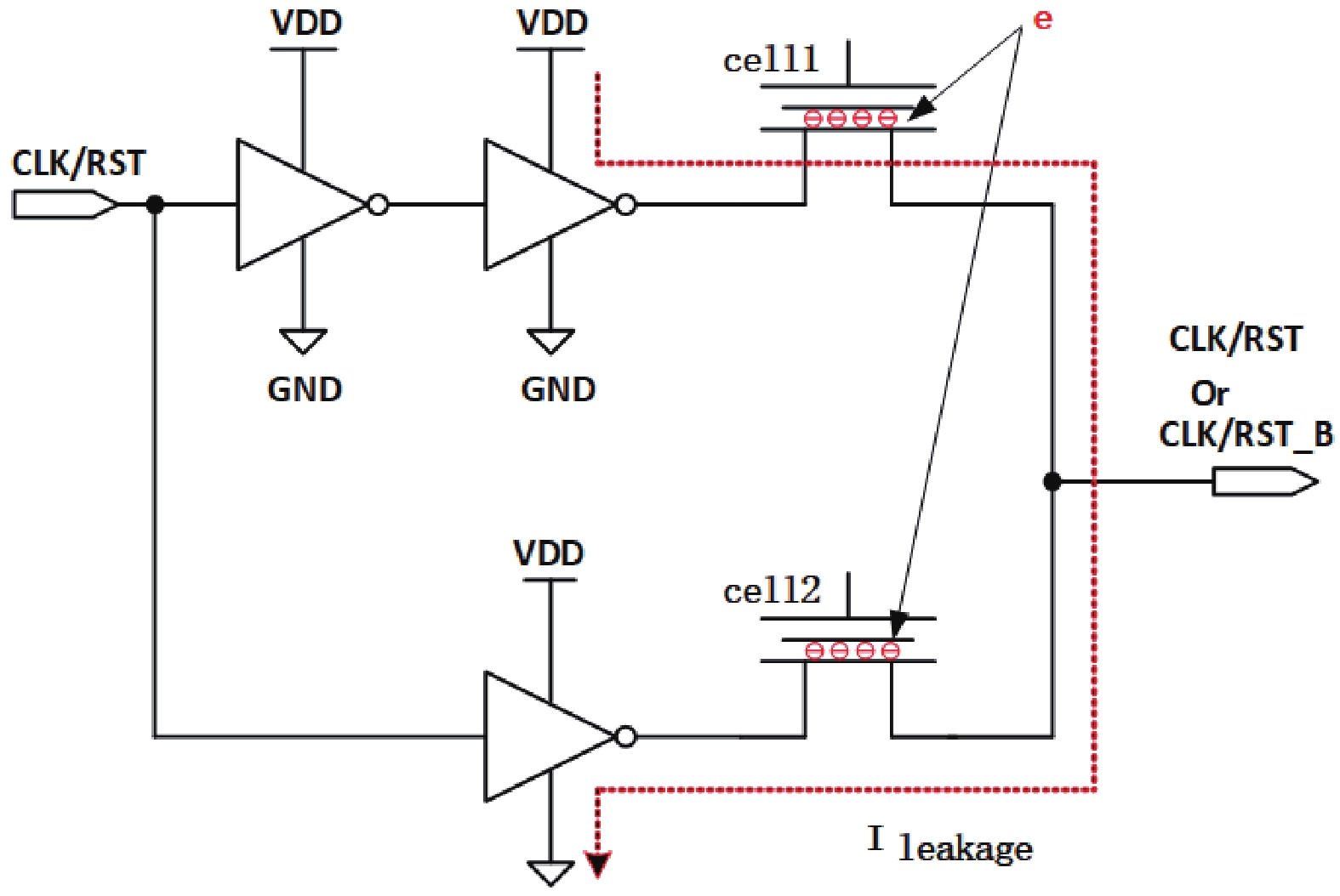
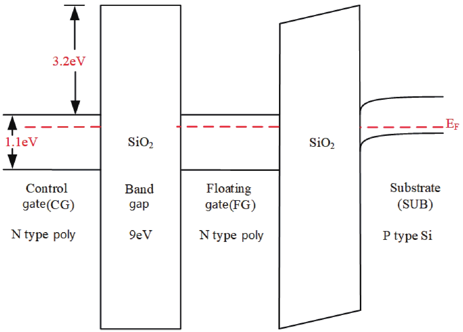
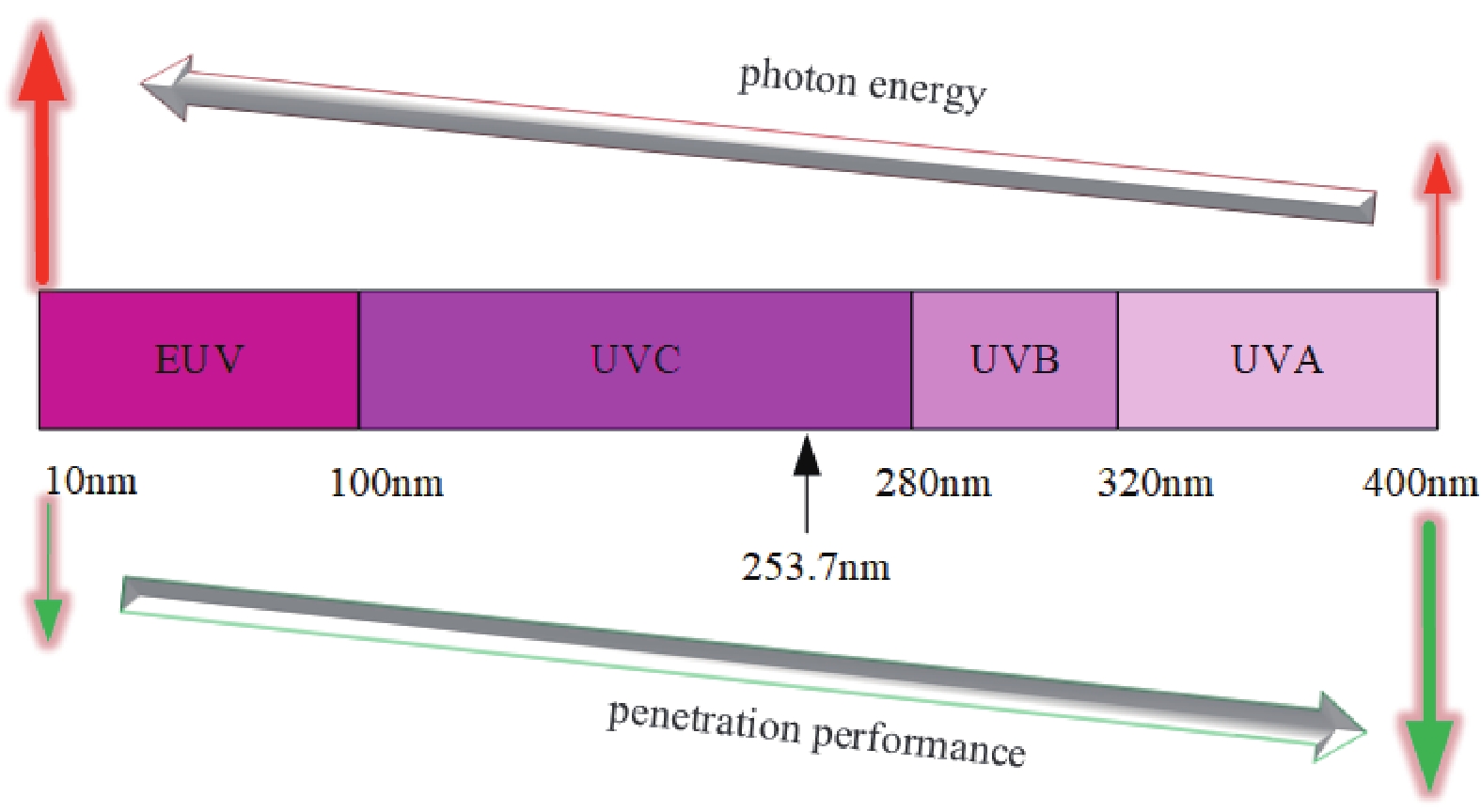
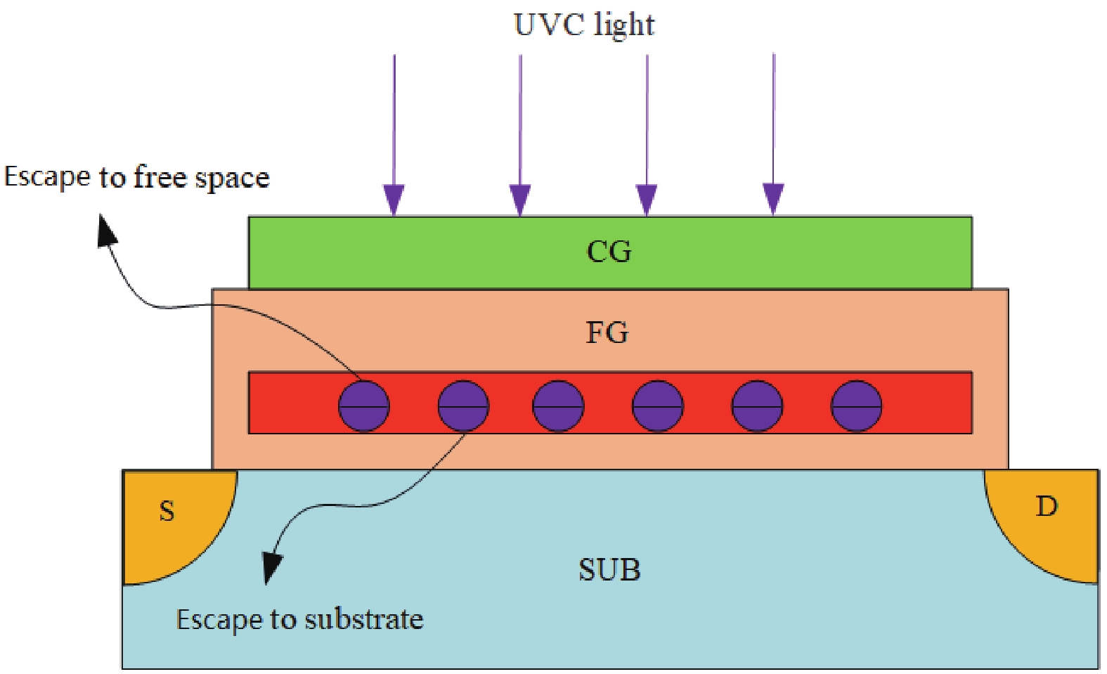
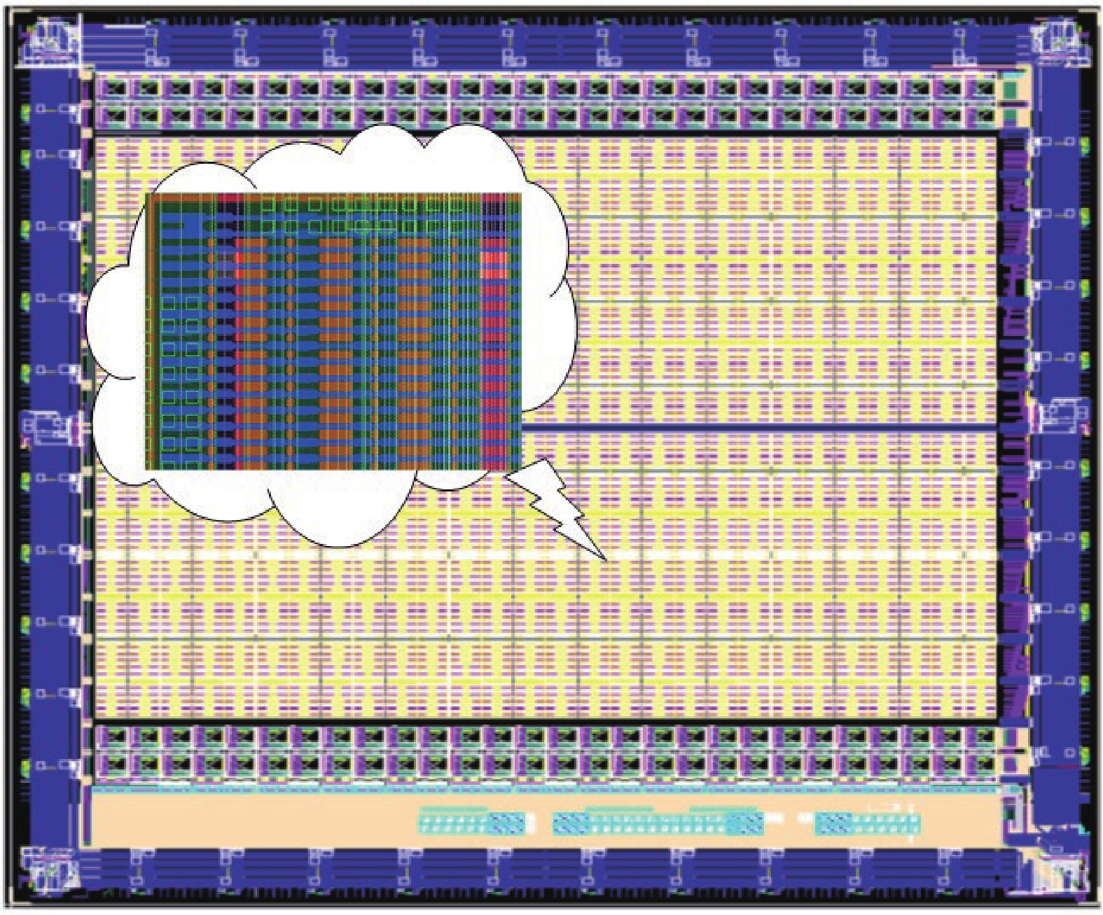
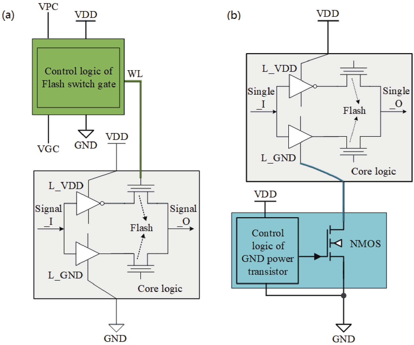
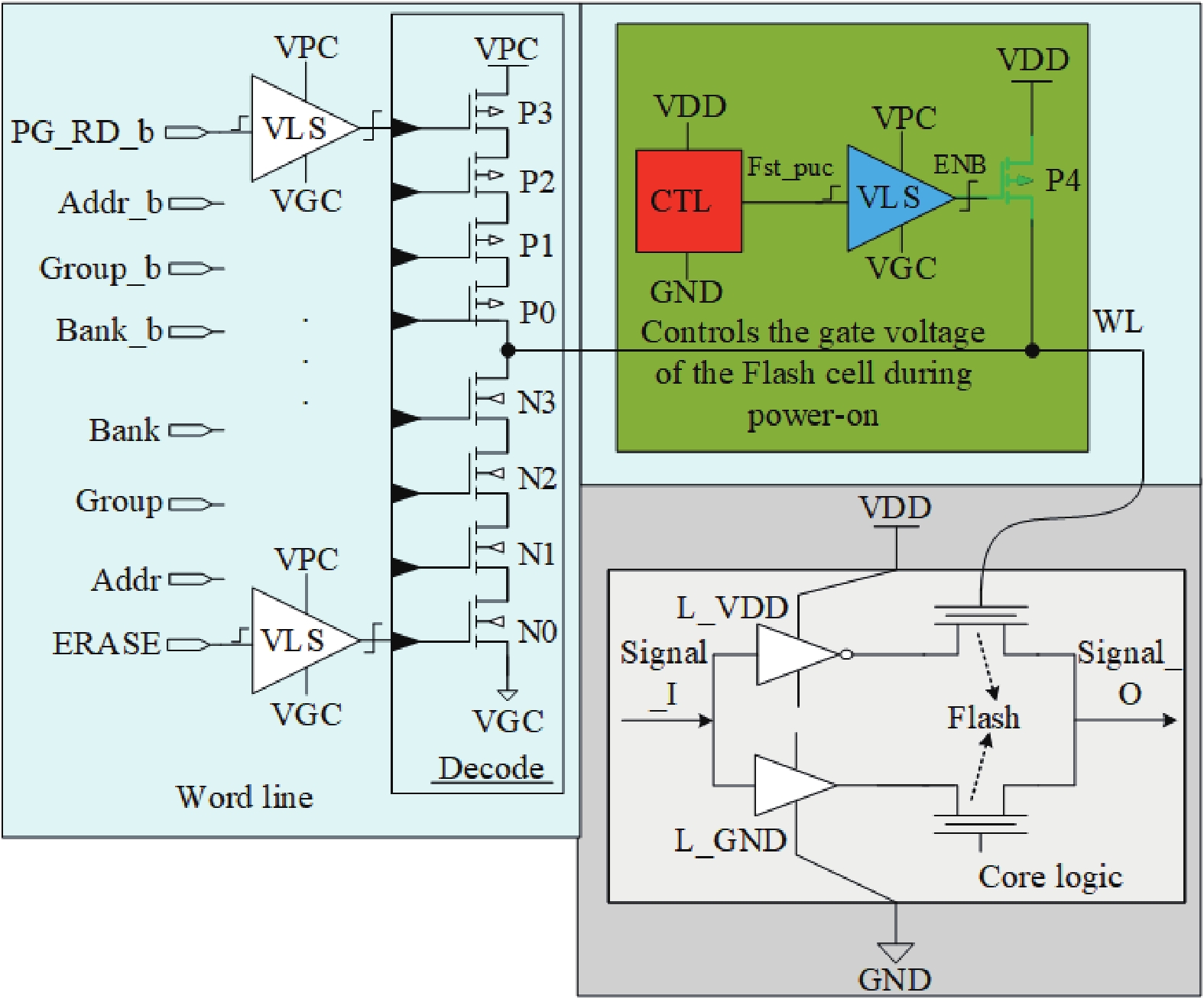
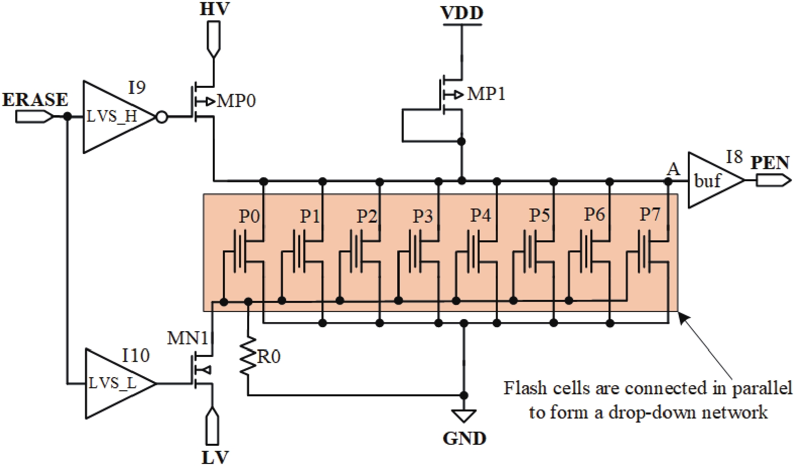
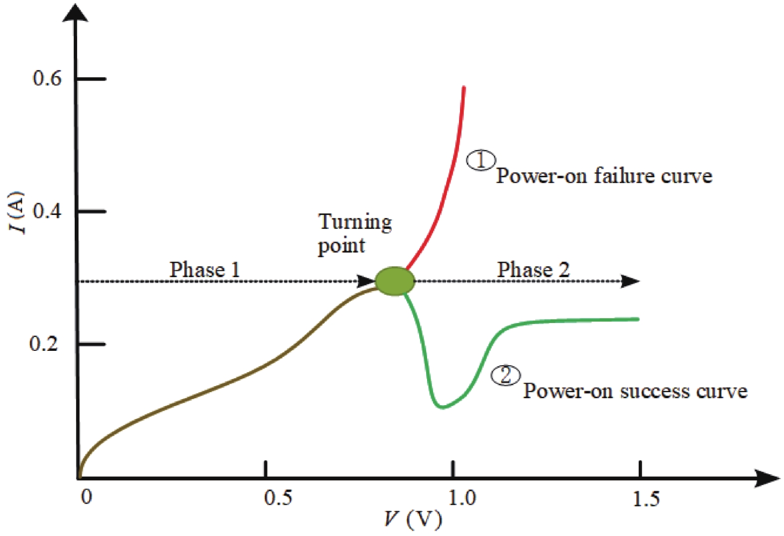
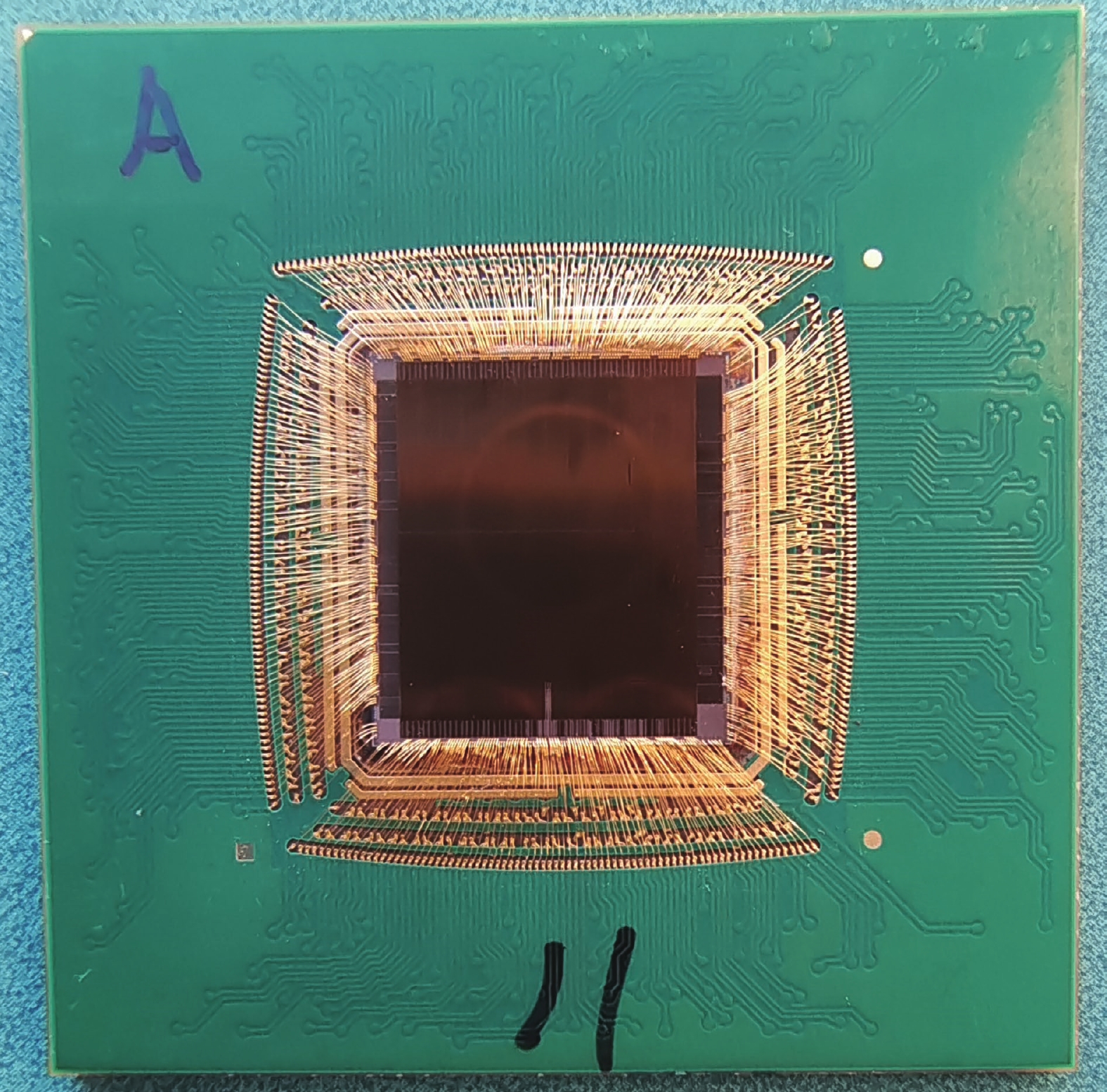
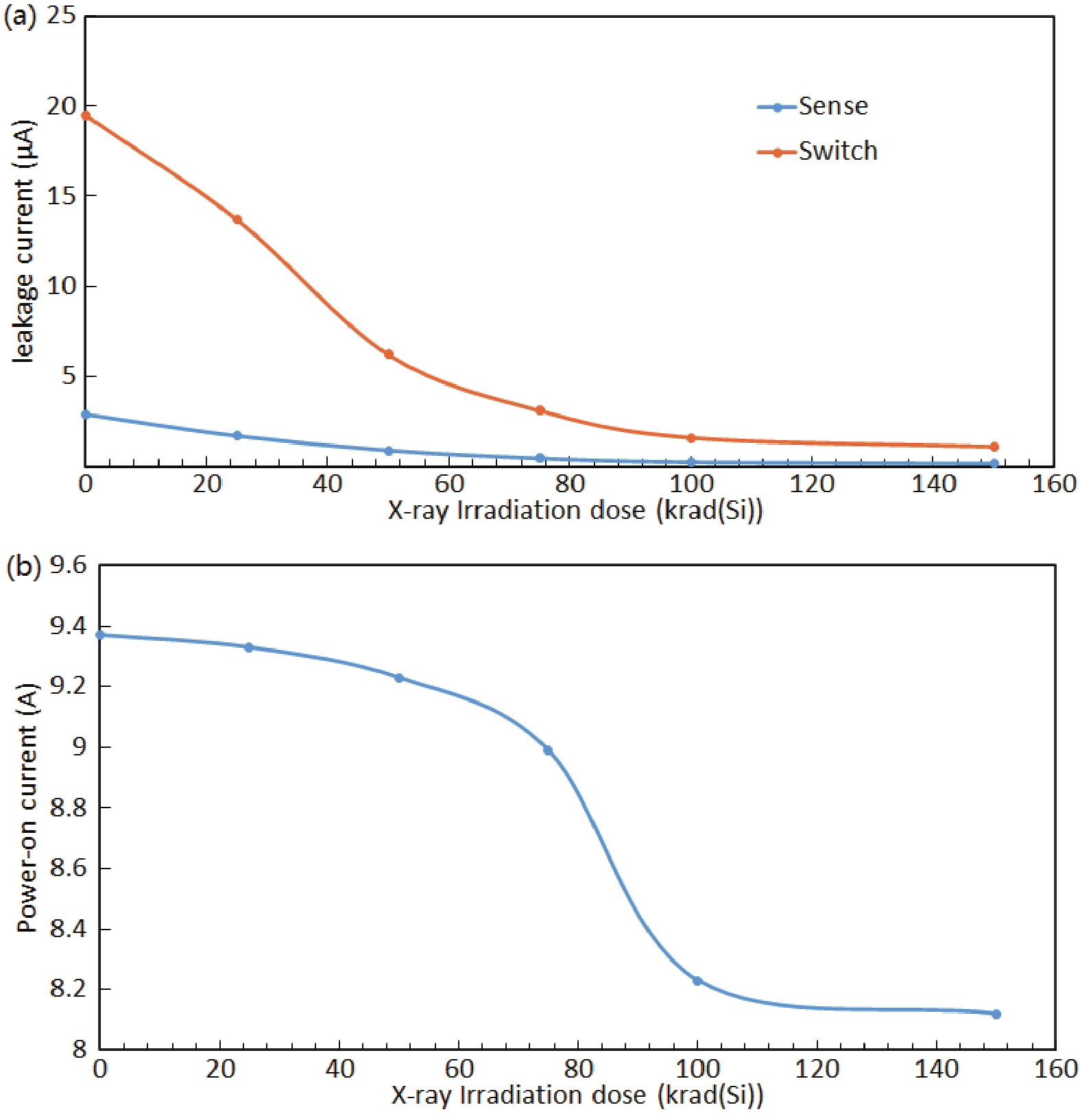
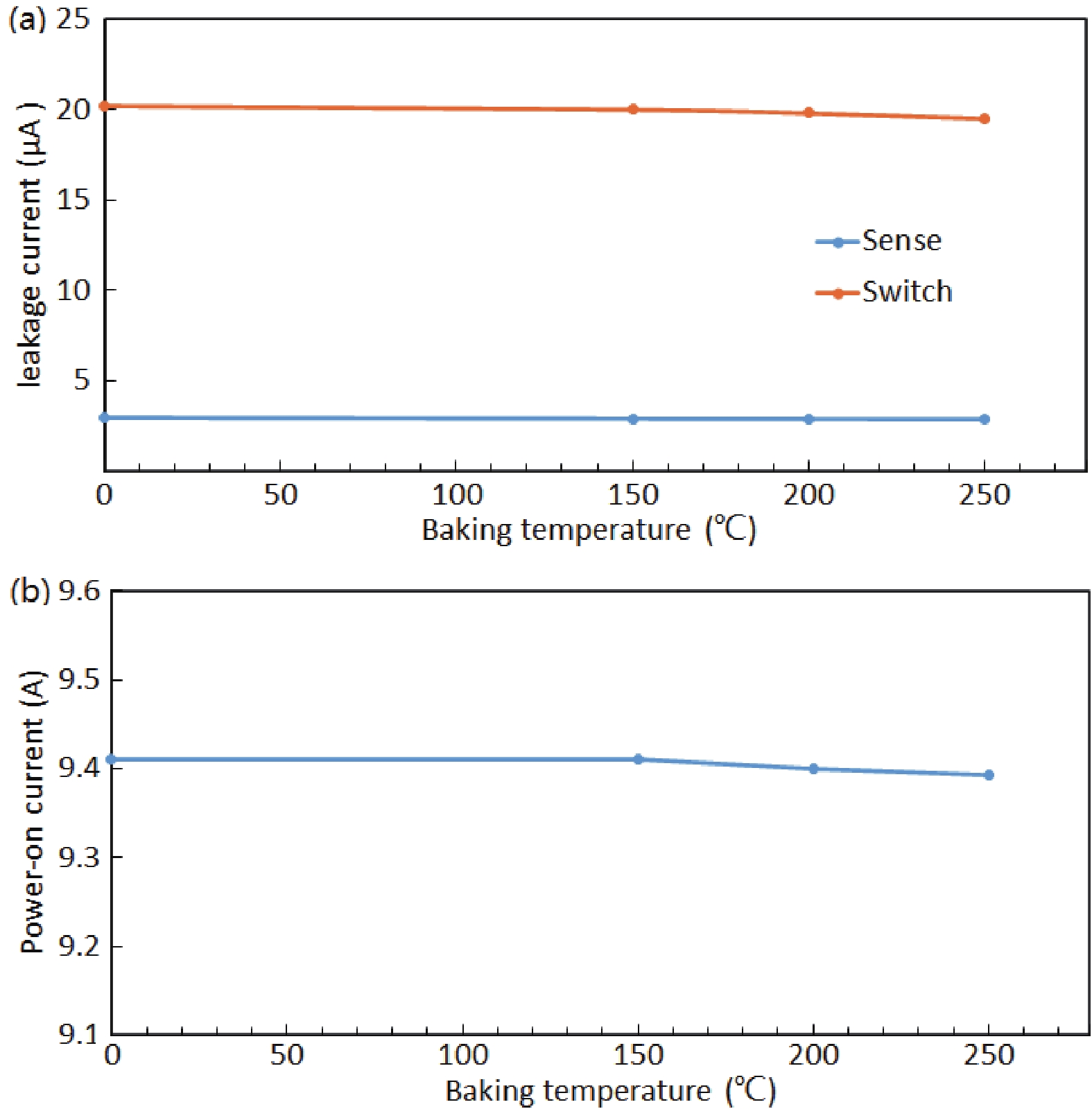
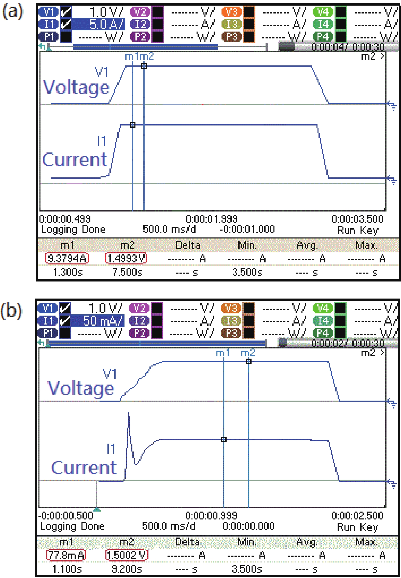
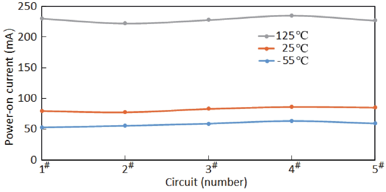
To solve the Flash-based FPGA in the manufacturing process, the ion implantation process will bring electrons into the floating gate of the P-channel Flash cell so that the Flash switch is in a weak conduction state, resulting in the Flash-based FPGA eigenstate current problem. In this paper, the mechanism of its generation is analyzed, and four methods are used including ultraviolet light erasing, high-temperature baking, X-ray irradiation, and circuit logic control. A comparison of these four methods can identify the circuit design by using circuit logic to control the path of the power supply that is the most suitable and reliable method to solve the Flash-based FPGA eigenstate current problem. By this method, the power-on current of 3.5 million Flash-based FPGA can be reduced to less than 0.3 A, and the chip can start normally. The function and performance of the chip can then be further tested and evaluated, which is one of the key technologies for developing Flash-based FPGA.


J. Semicond.
2022, 43(12): 122701 doi: 10.1088/1674-4926/43/12/122701

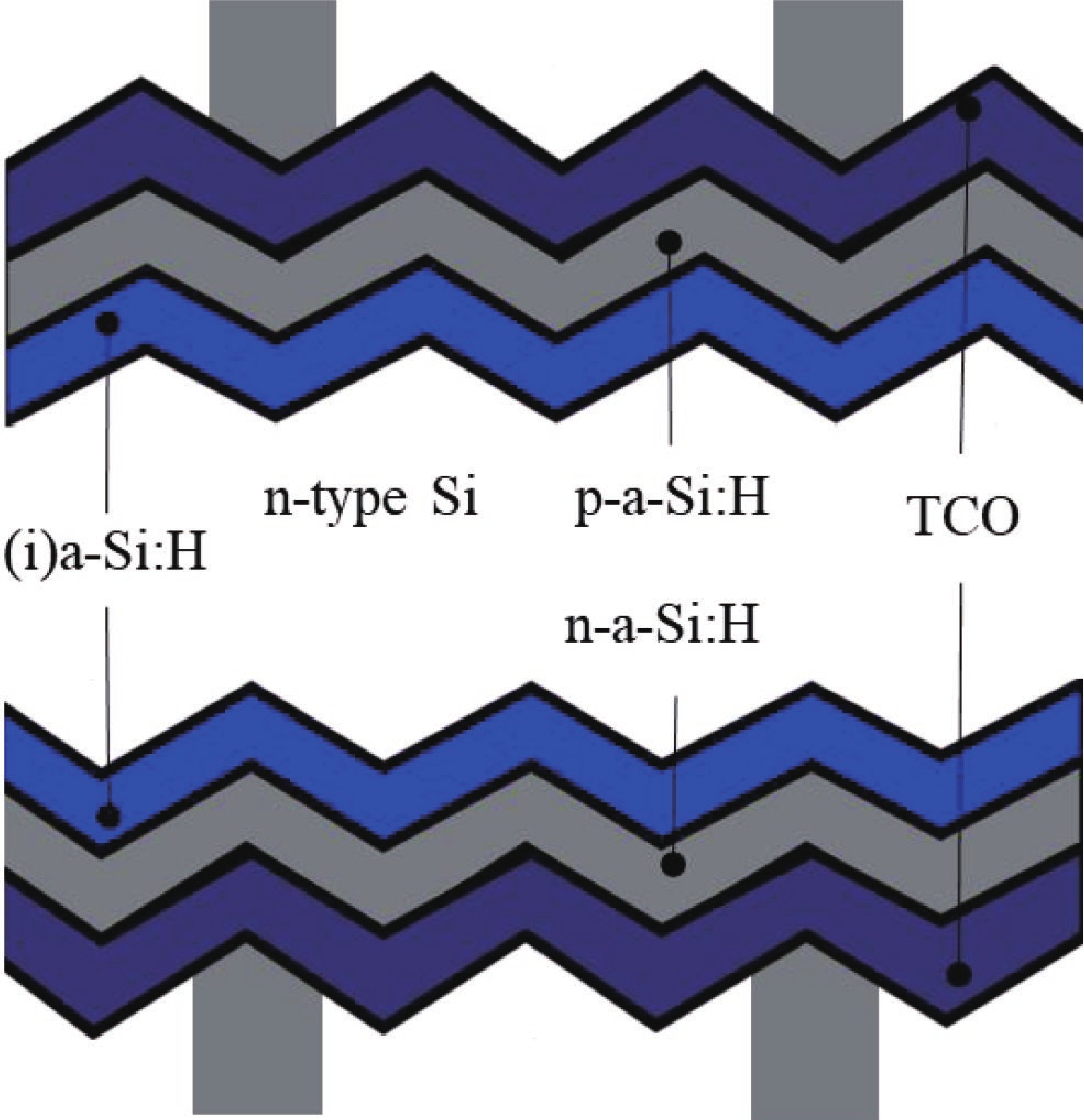
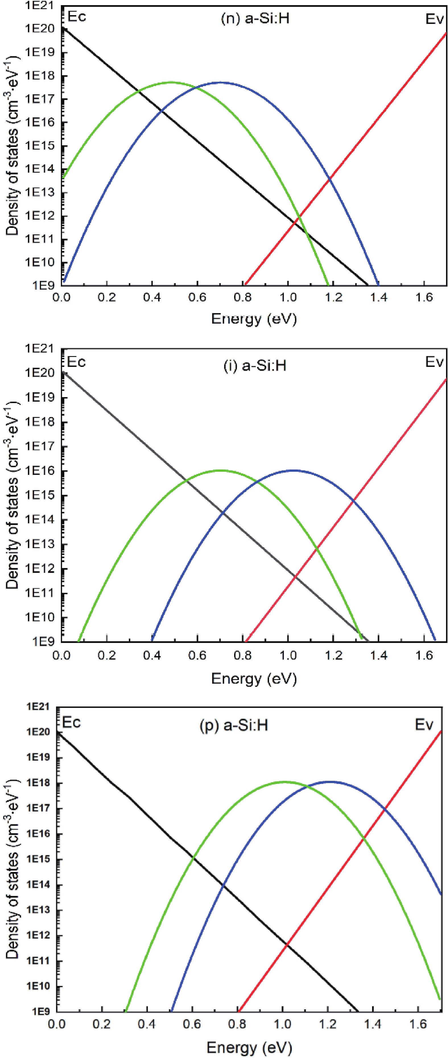
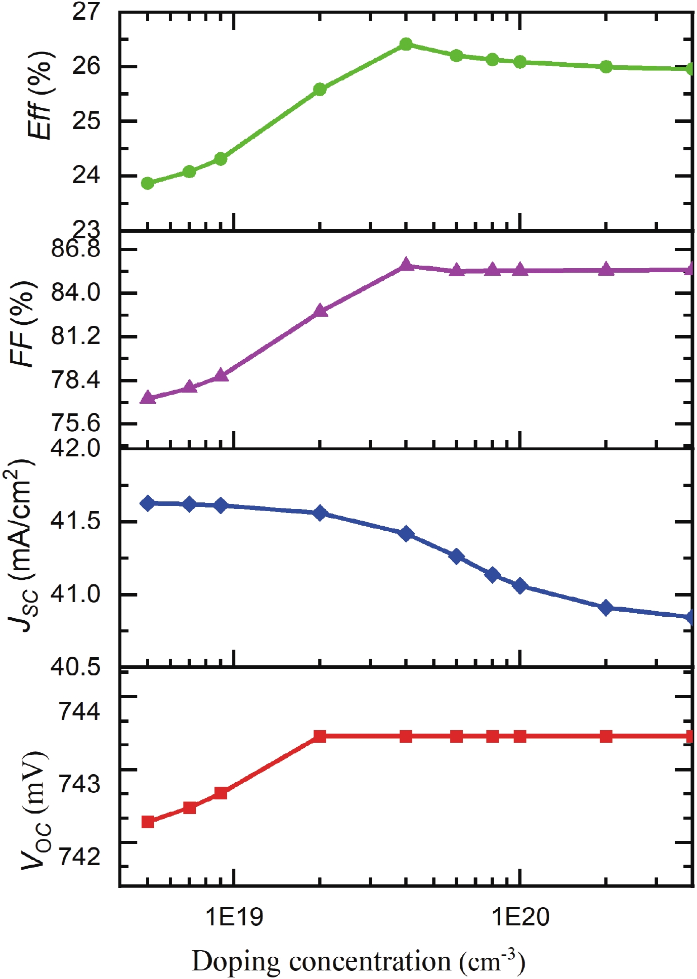
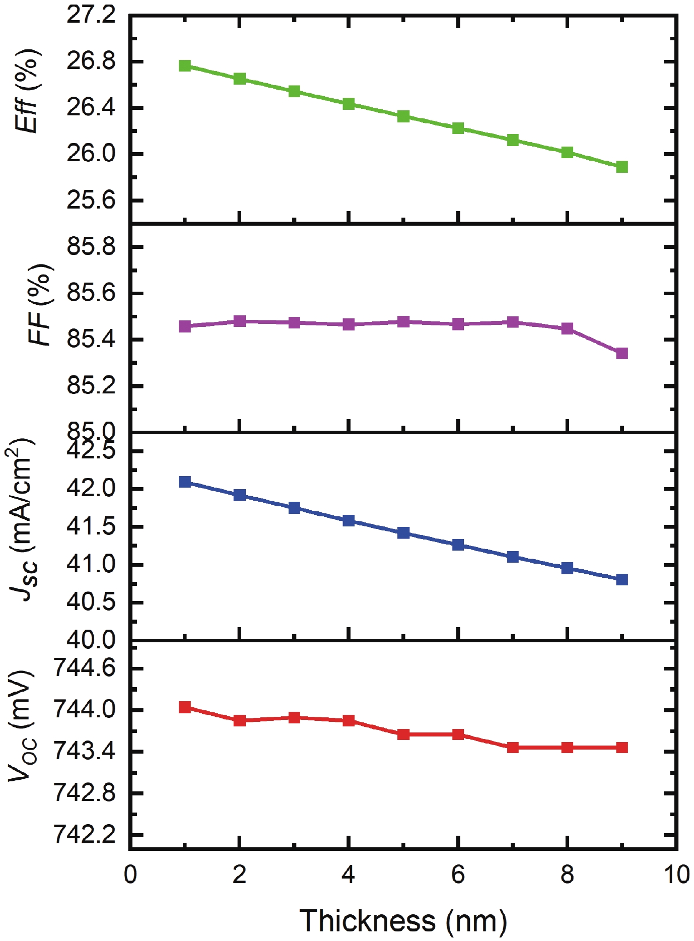
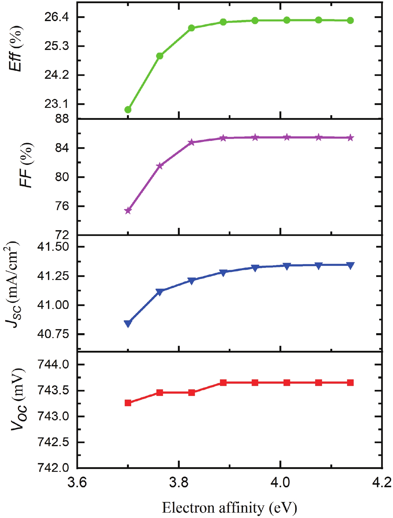
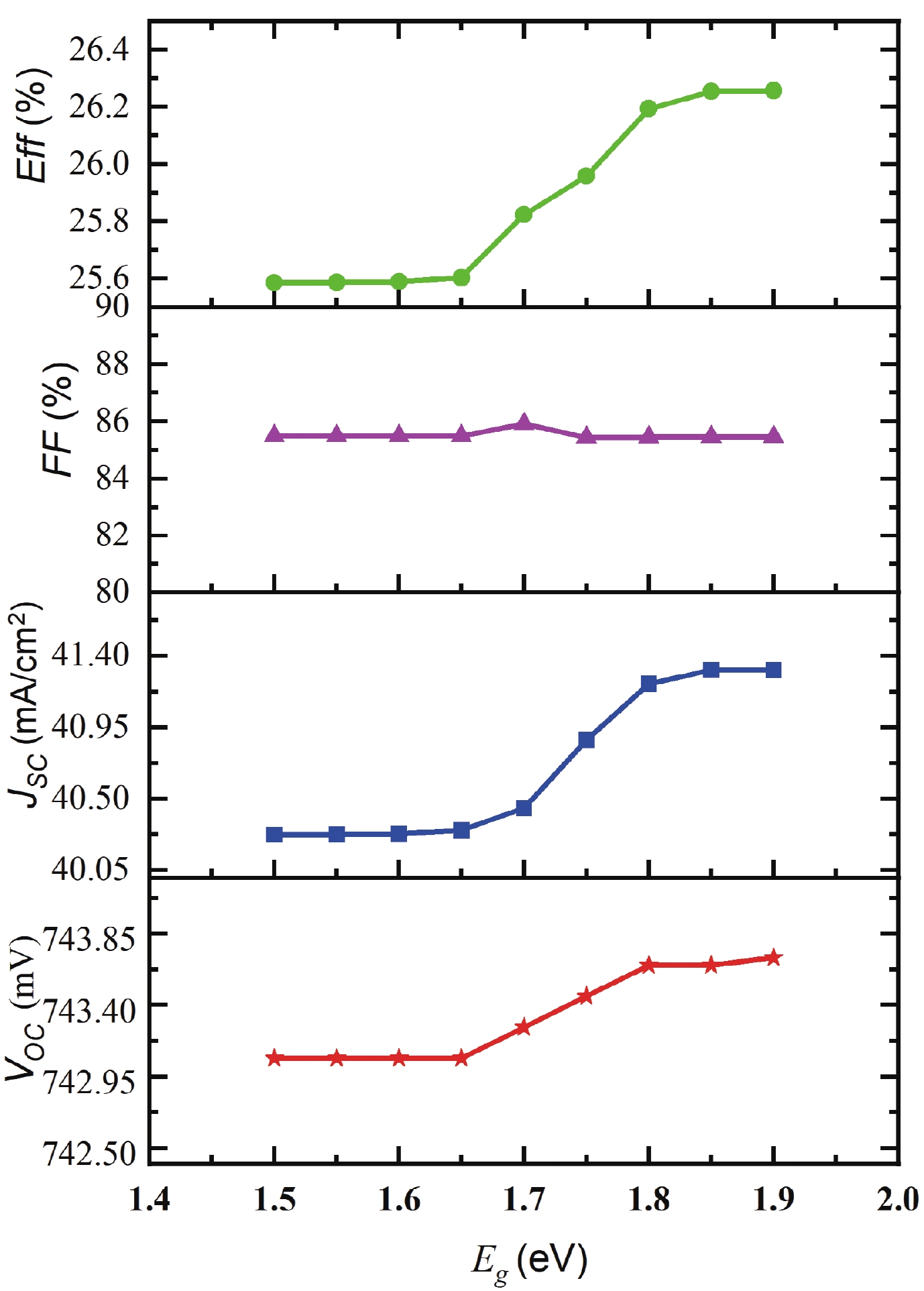
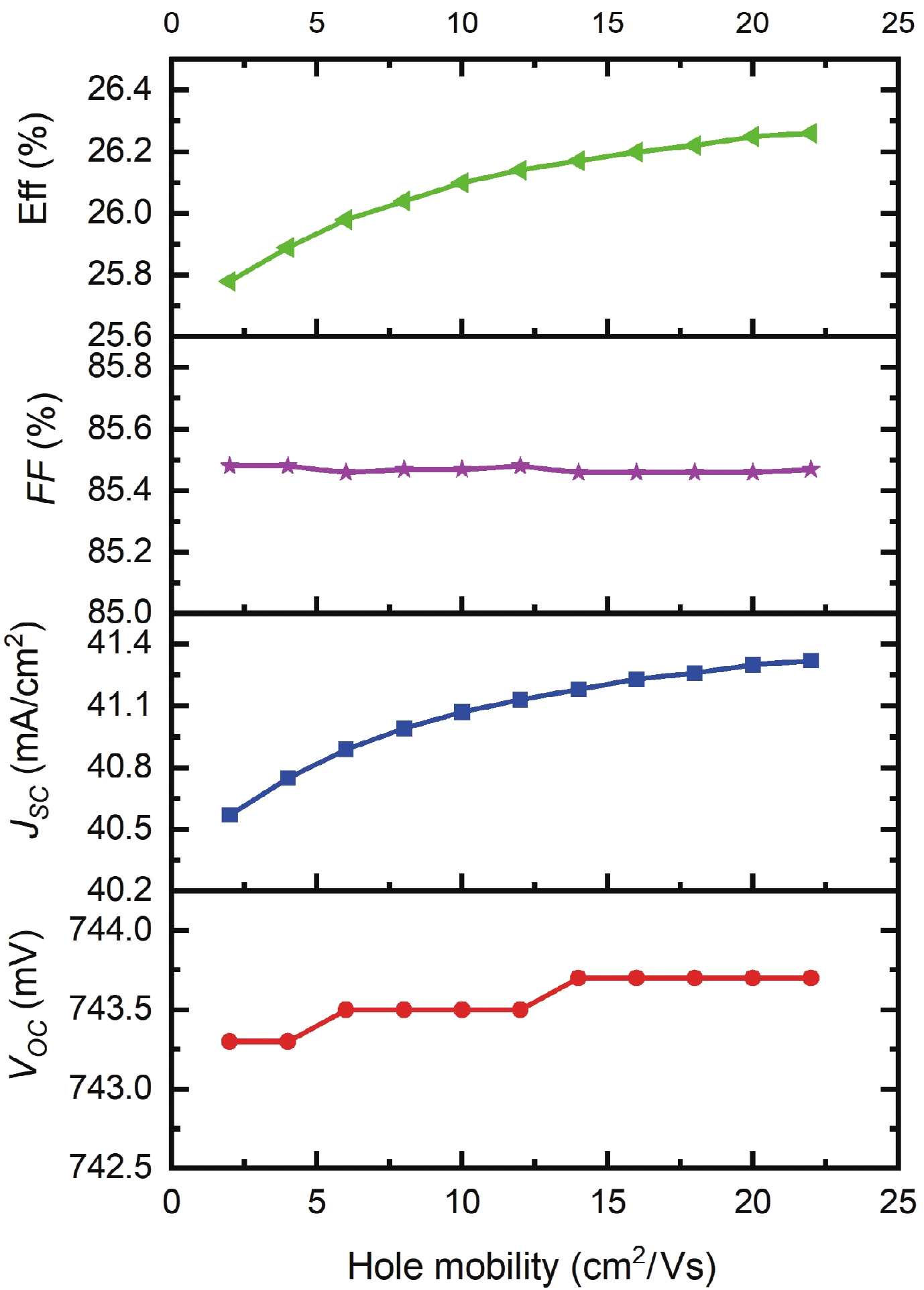
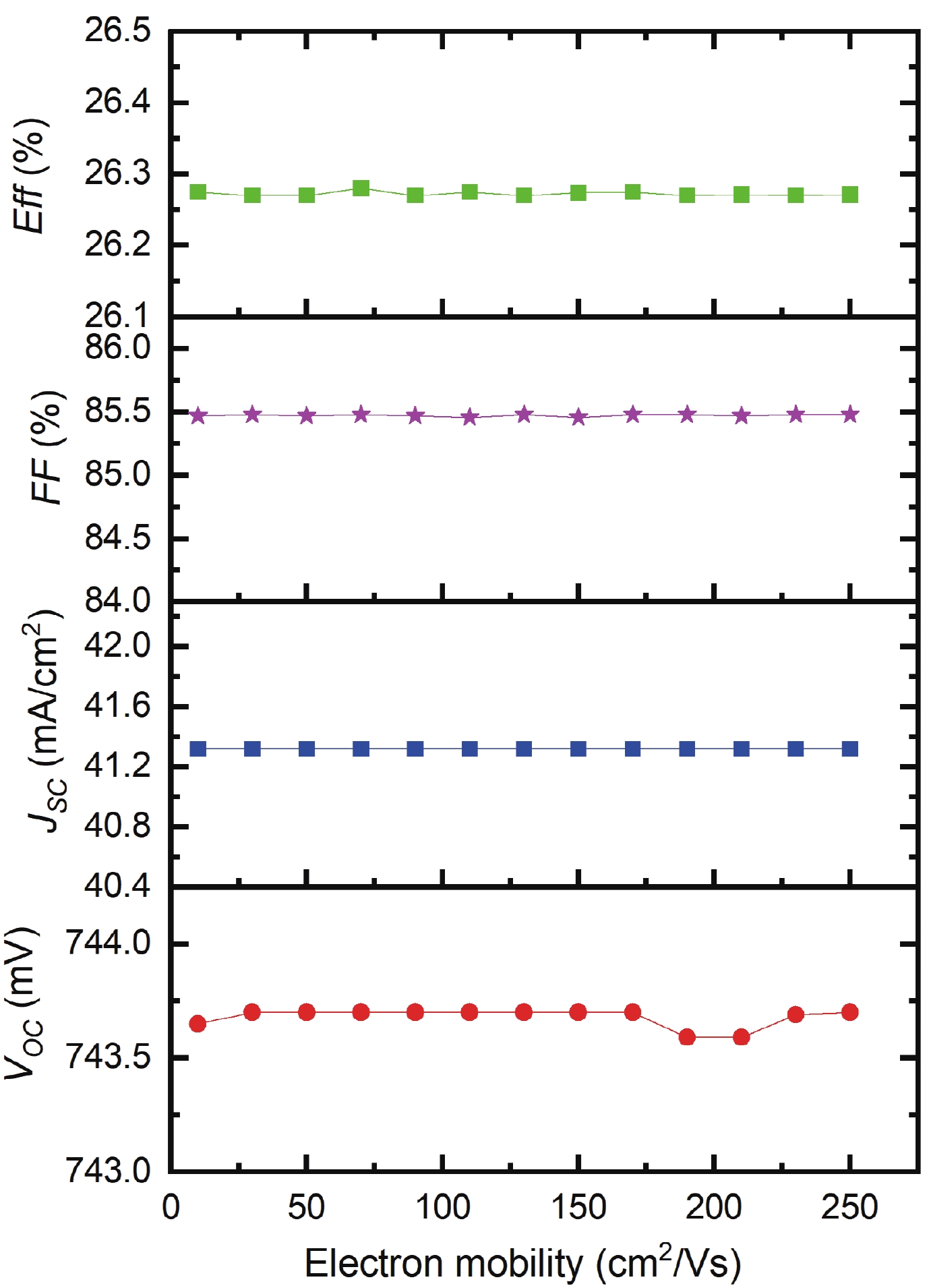
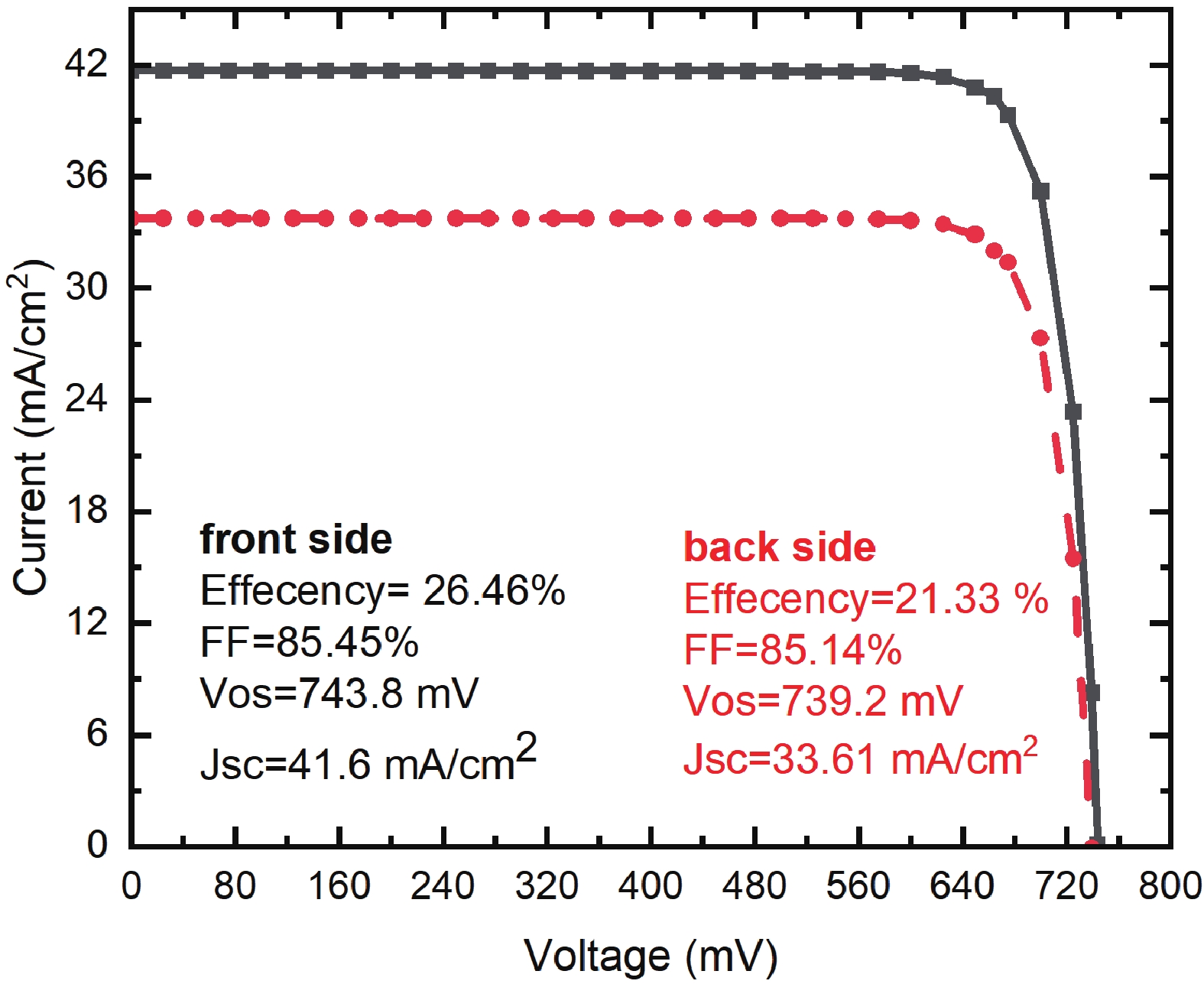
Silicon solar cells continue to dominate the market, due to the abundance of silicon and their acceptable efficiency. The heterojunction with intrinsic thin layer (HIT) structure is now the dominant technology. Increasing the efficiency of these cells could expand the development choices for HIT solar cells. We presented a detailed investigation of the emitter a-Si:H(n) layer of a p-type bifacial HIT solar cell in terms of characteristic parameters which include layer doping concentration, thickness, band gap width, electron affinity, hole mobility, and so on. Solar cell composition: (ZnO/nc-Si:H(n)/a-Si:H(i)/c-Si(p)/a-Si:H(i)/nc-Si:H(p)/ZnO). The results reveal optimal values for the investigated parameters, for which the highest computed efficiency is 26.45% when lighted from the top only and 21.21% when illuminated from the back only.


J. Semicond.
2022, 43(12): 122801 doi: 10.1088/1674-4926/43/12/122801
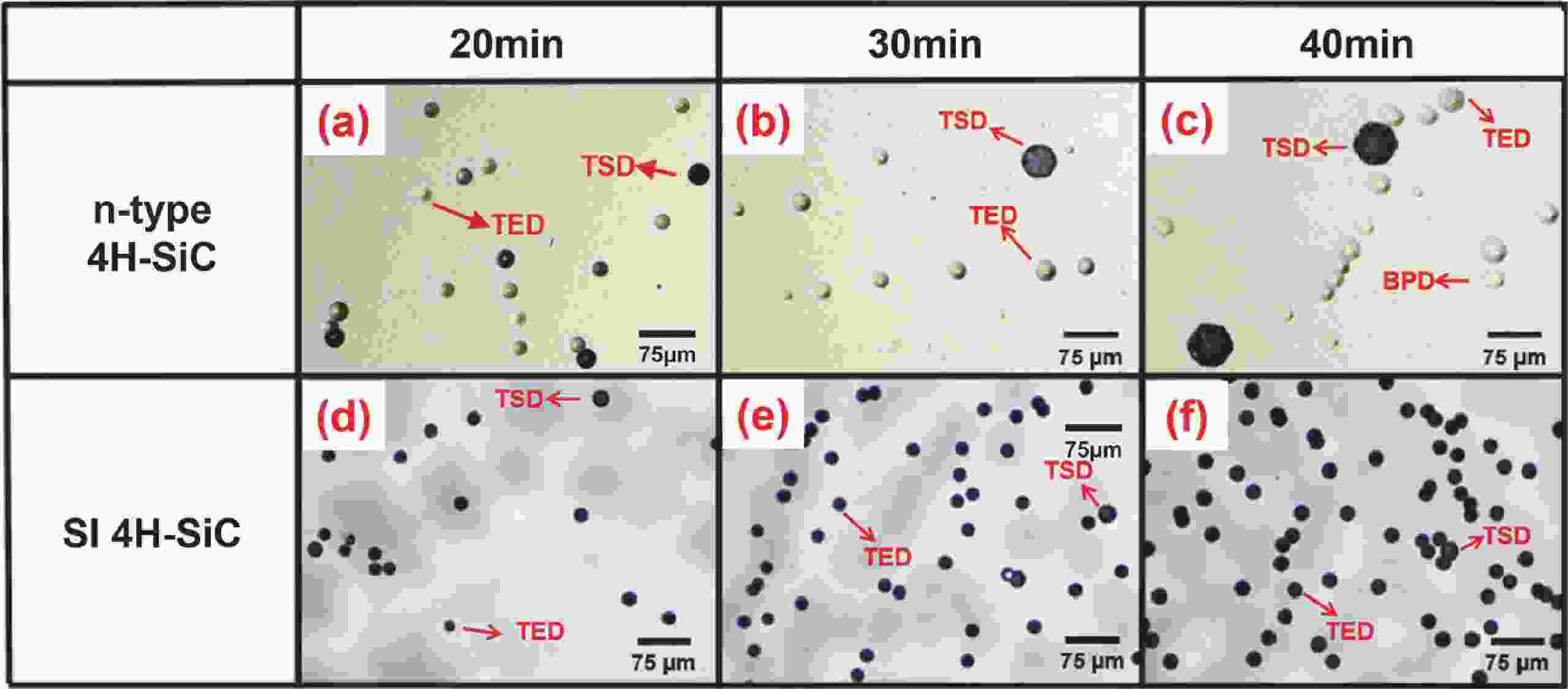
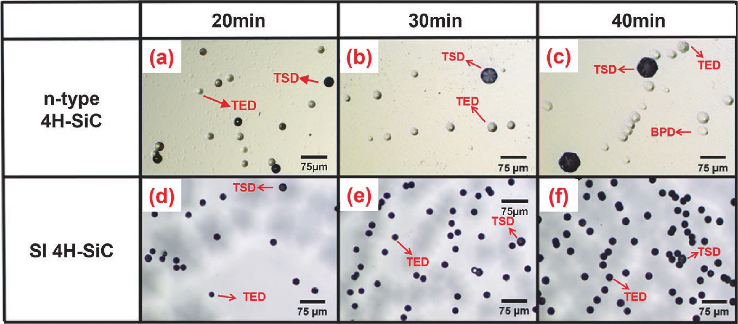
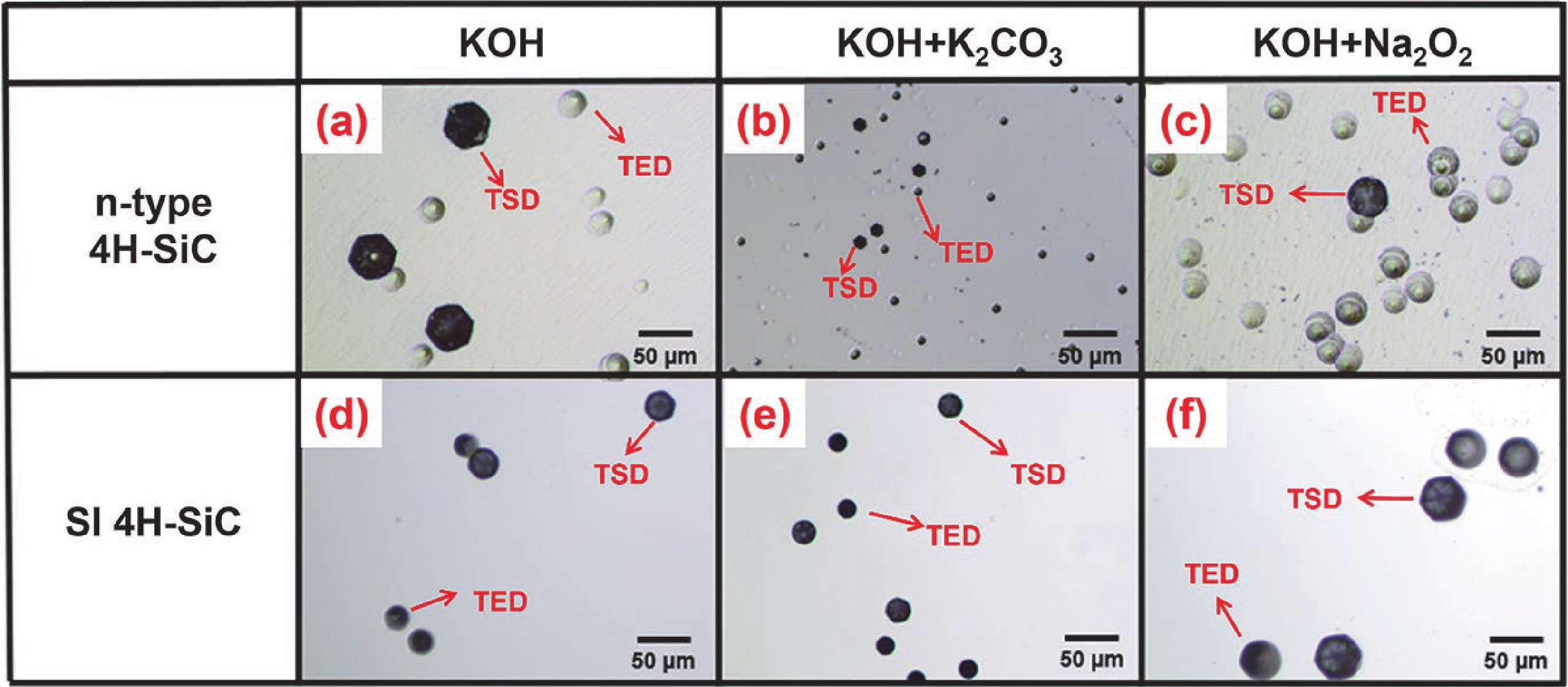
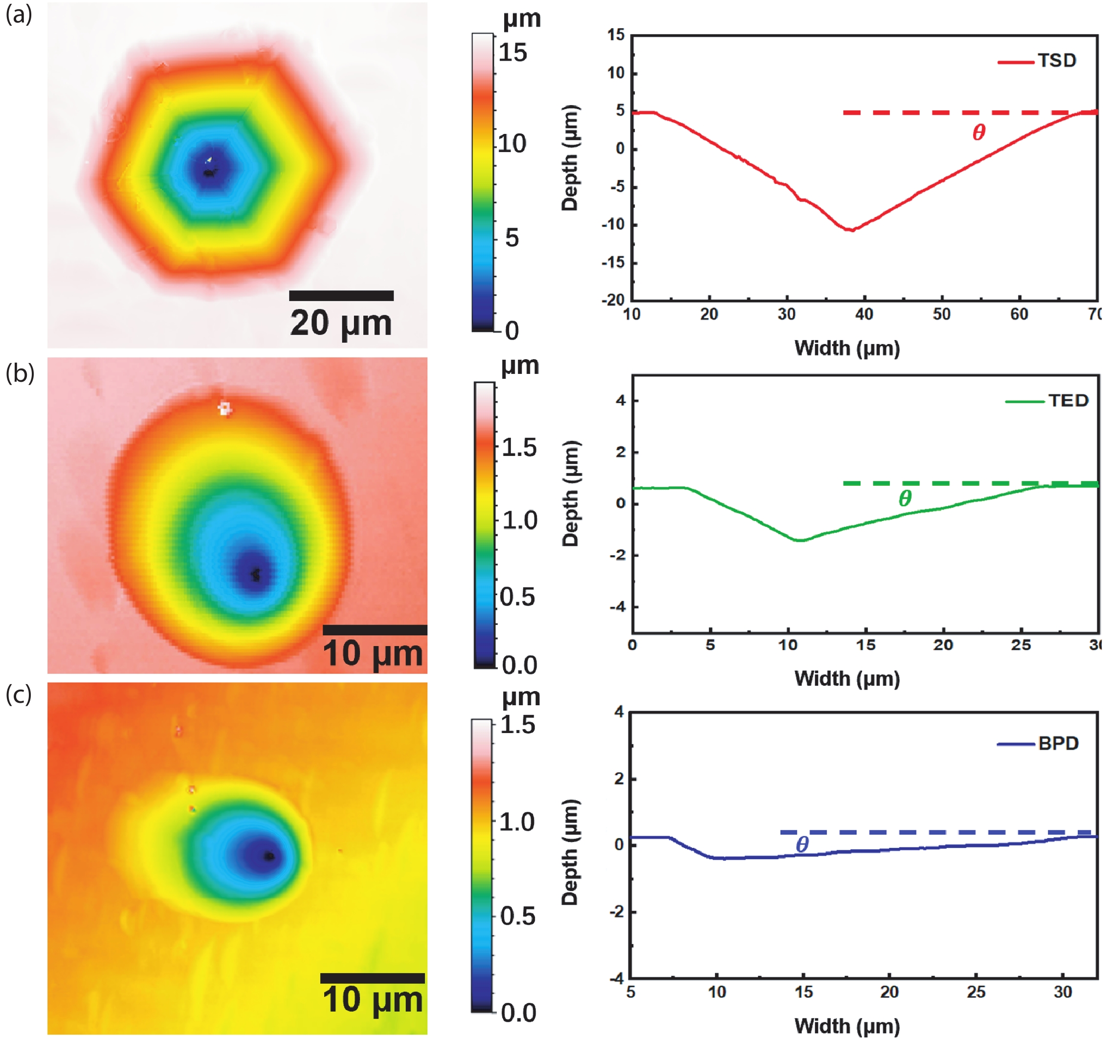
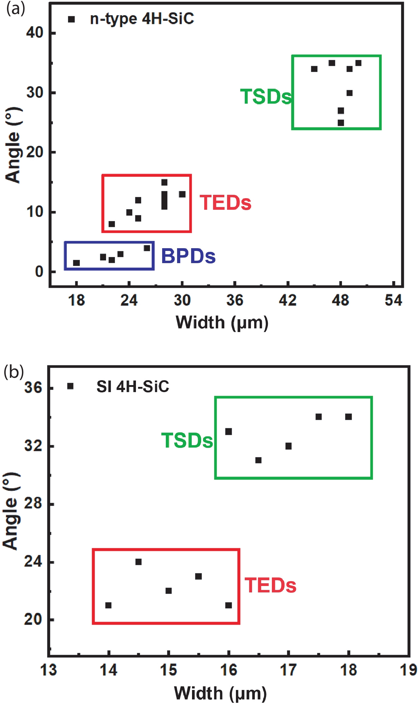
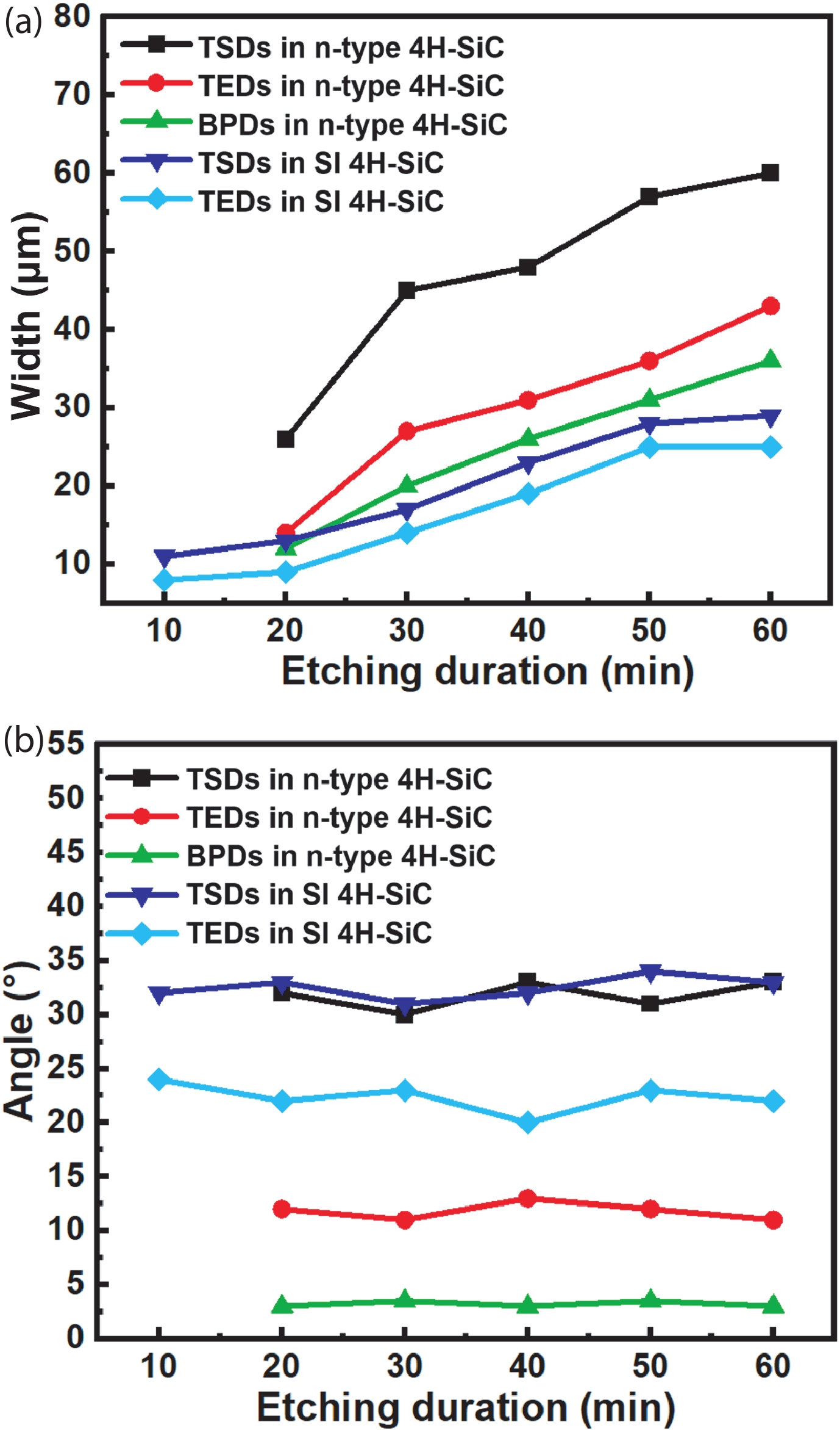
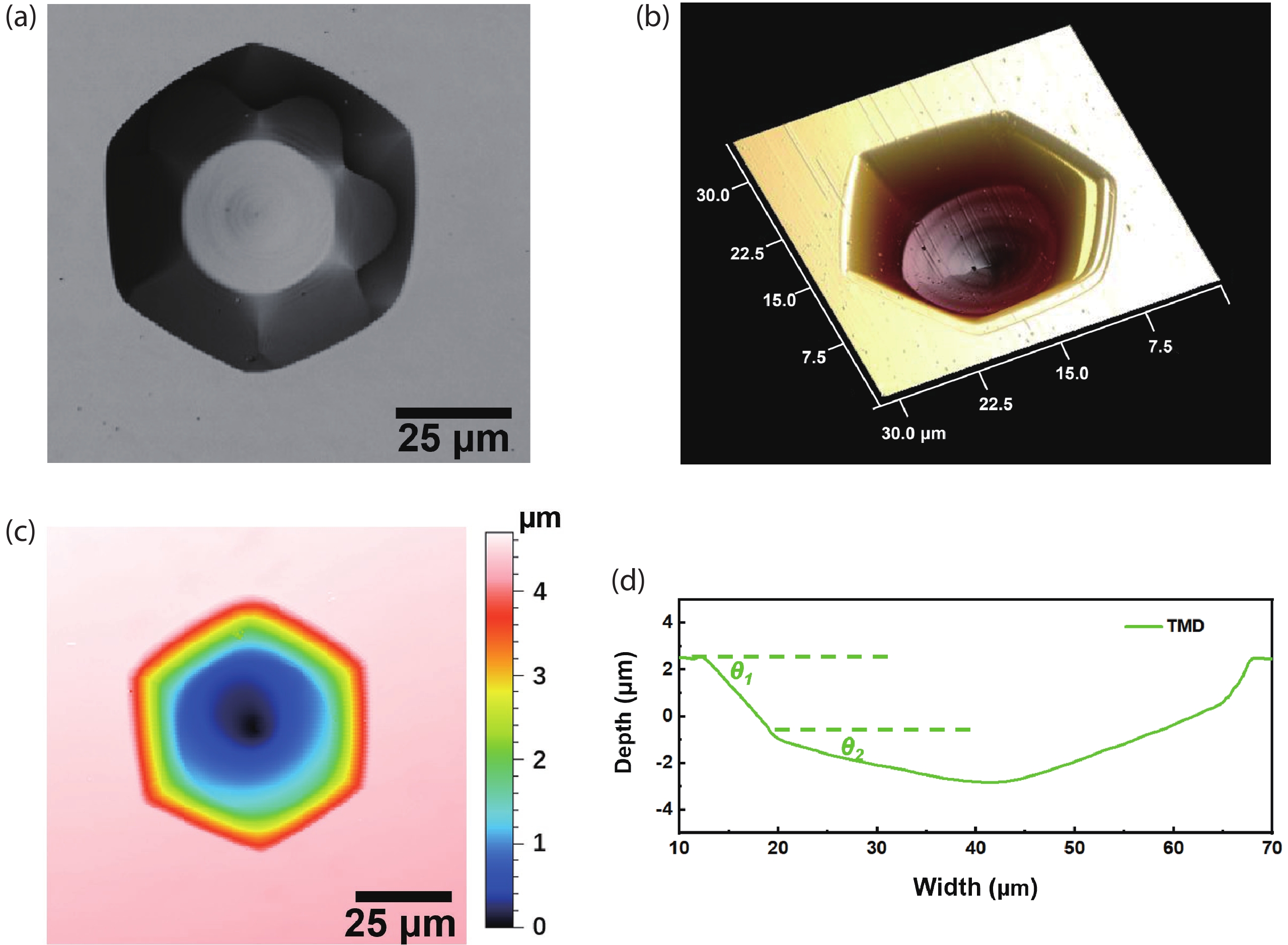
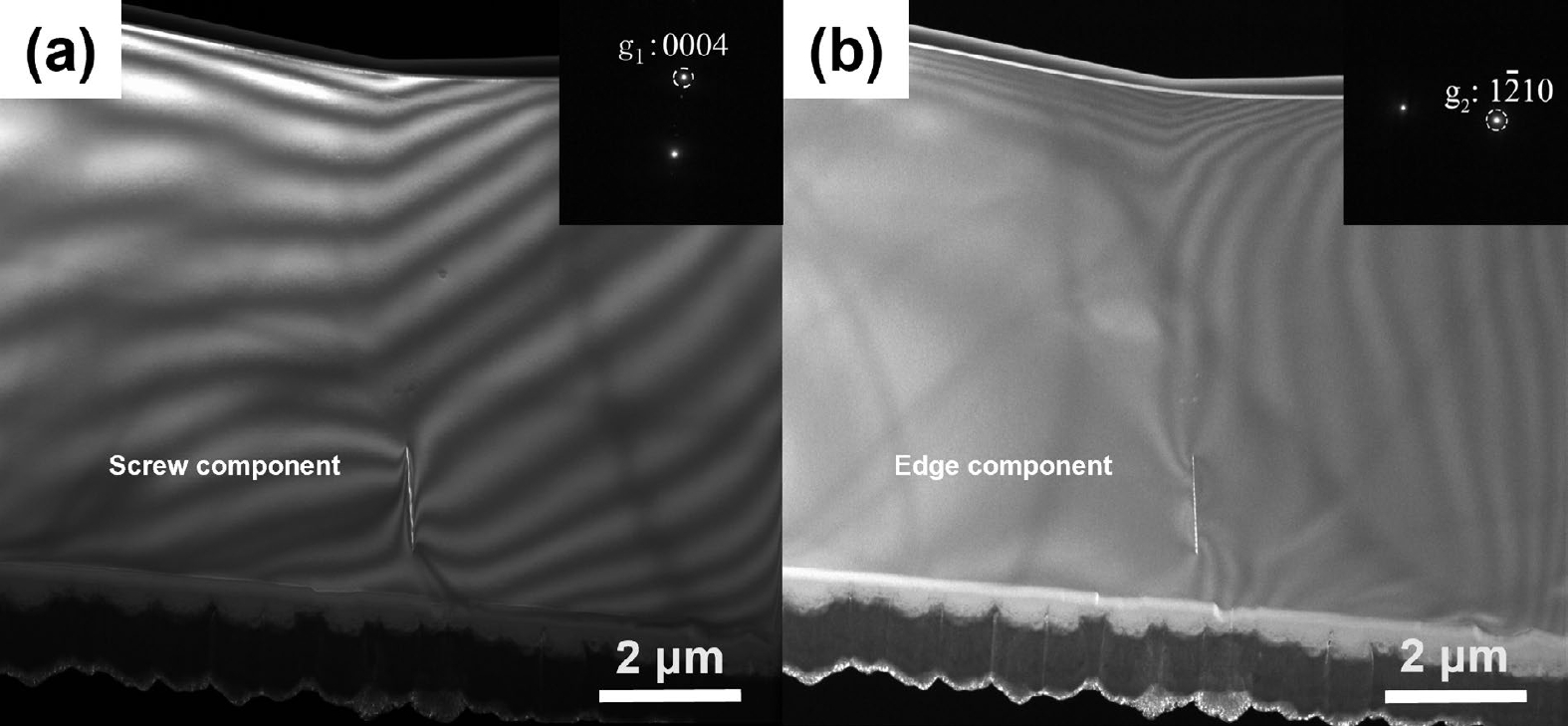
Discrimination of dislocations is critical to the statistics of dislocation densities in 4H silicon carbide (4H-SiC), which are routinely used to evaluate the quality of 4H-SiC single crystals and homoepitaxial layers. In this work, we show that the inclination angles of the etch pits of molten-alkali etched 4H-SiC can be adopted to discriminate threading screw dislocations (TSDs), threading edge dislocations (TEDs) and basal plane dislocations (BPDs) in 4H-SiC. In n-type 4H-SiC, the inclination angles of the etch pits of TSDs, TEDs and BPDs in molten-alkali etched 4H-SiC are in the ranges of 27°−35°, 8°−15° and 2°−4°, respectively. In semi-insulating 4H-SiC, the inclination angles of the etch pits of TSDs and TEDs are in the ranges of 31°−34° and 21°−24°, respectively. The inclination angles of dislocation-related etch pits are independent of the etching duration, which facilitates the discrimination and statistic of dislocations in 4H-SiC. More significantly, the inclination angle of a threading mixed dislocations (TMDs) is found to consist of characteristic angles of both TEDs and TSDs. This enables to distinguish TMDs from TSDs in 4H-SiC.
J. Semicond.
2022, 43(12): 122802 doi: 10.1088/1674-4926/43/12/122802

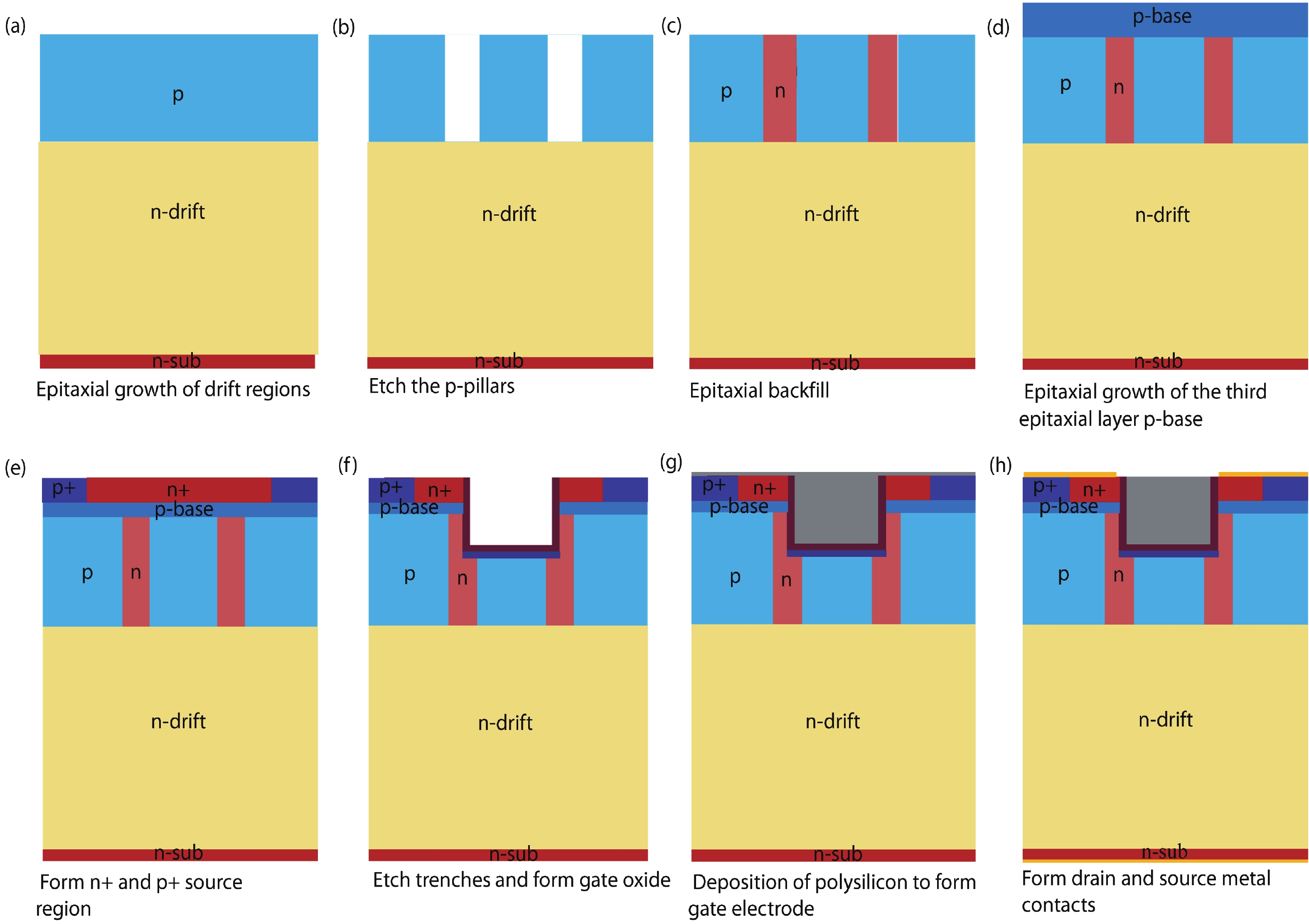
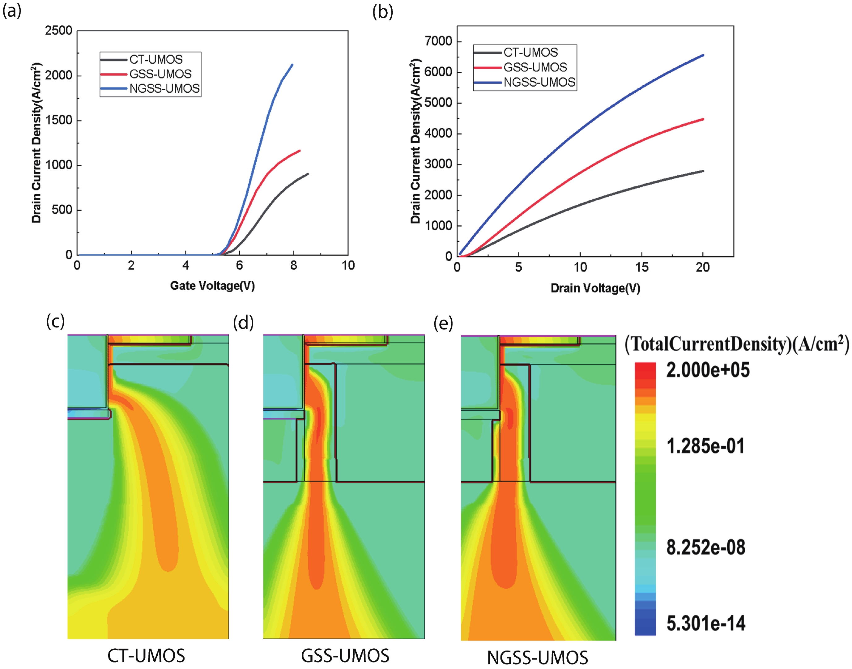
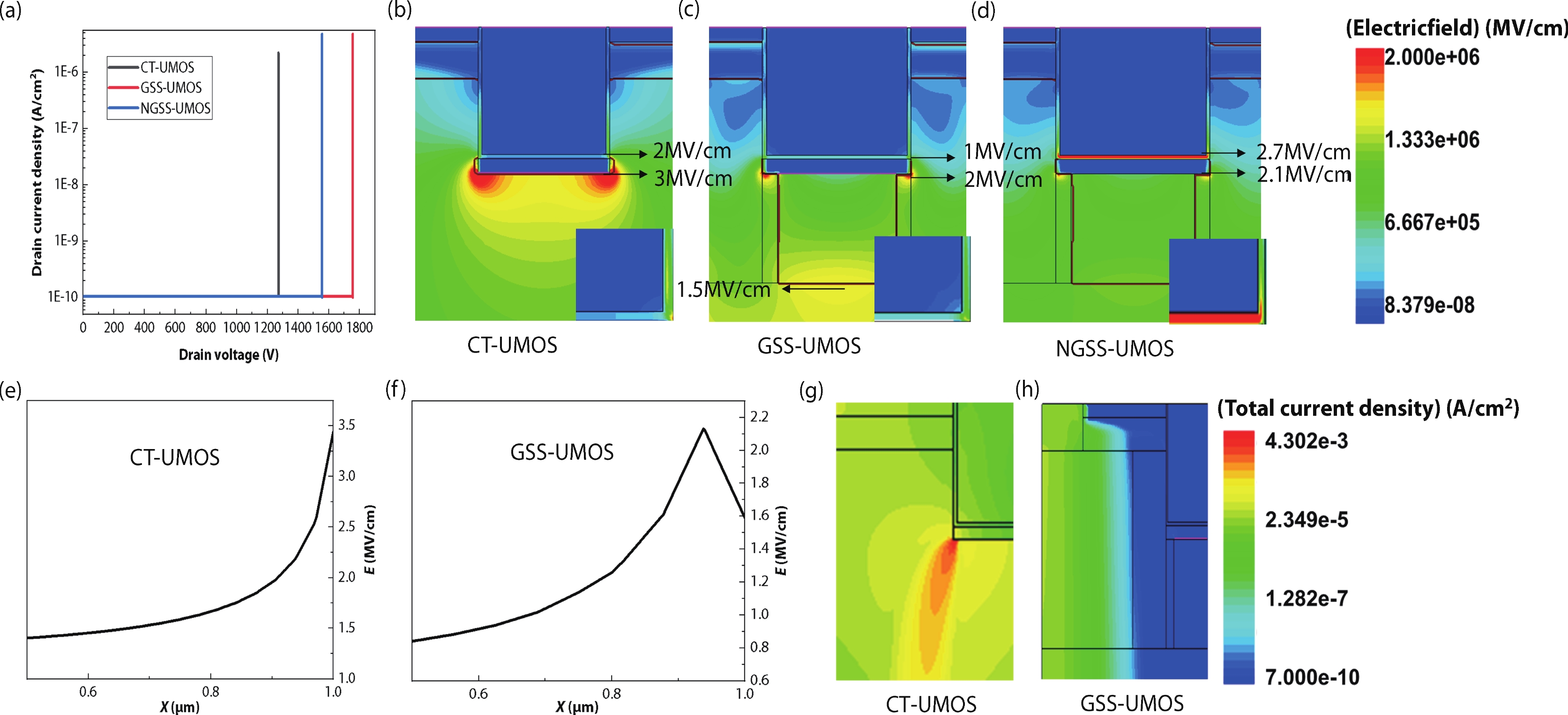
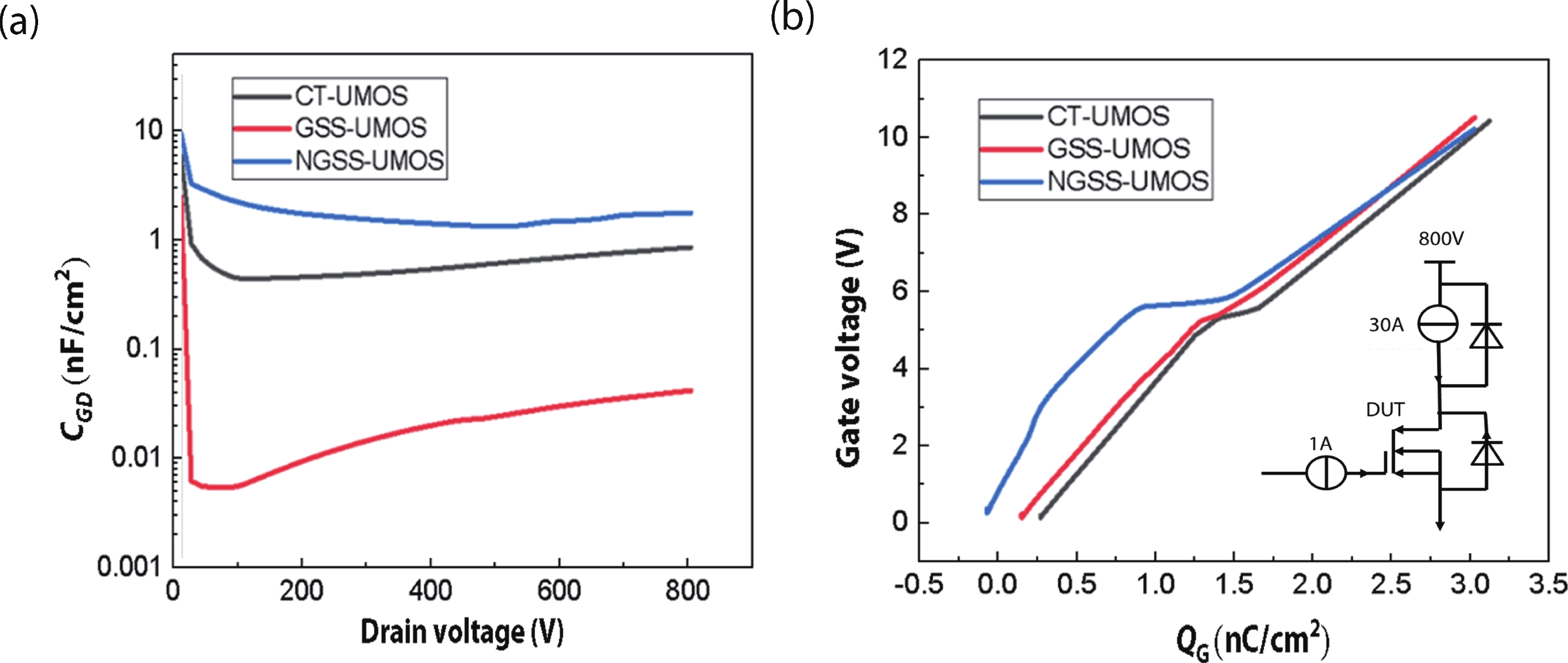
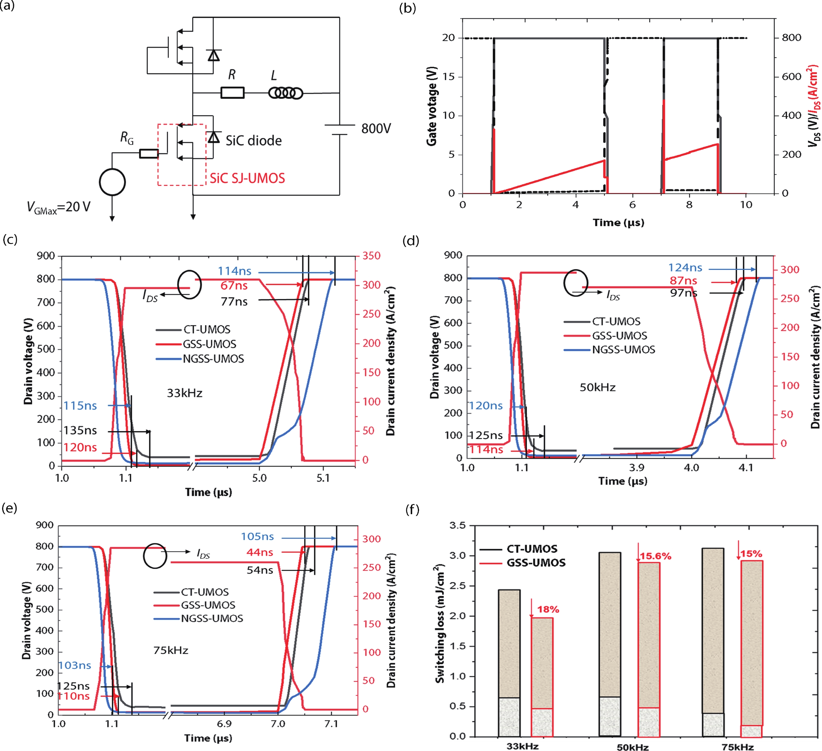
A 4H-SiC trench gate metal–oxide–semiconductor field-effect transistor (UMOSFET) with semi-super-junction shielded structure (SS-UMOS) is proposed and compared with conventional trench MOSFET (CT-UMOS) in this work. The advantage of the proposed structure is given by comprehensive study of the mechanism of the local semi-super-junction structure at the bottom of the trench MOSFET. In particular, the influence of the bias condition of the p-pillar at the bottom of the trench on the static and dynamic performances of the device is compared and revealed. The on-resistance of SS-UMOS with grounded (G) and ungrounded (NG) p-pillar is reduced by 52% (G) and 71% (NG) compared to CT-UMOS, respectively. Additionally, gate oxide in the GSS-UMOS is fully protected by the p-shield layer as well as semi-super-junction structure under the trench and p-base regions. Thus, a reduced electric-field of 2 MV/cm can be achieved at the corner of the p-shield layer. However, the quasi-intrinsic protective layer cannot be formed in NGSS-UMOS due to the charge storage effect in the floating p-pillar, resulting in a large electric field of 2.7 MV/cm at the gate oxide layer. Moreover, the total switching loss of GSS-UMOS is 1.95 mJ/cm2 and is reduced by 18% compared with CT-UMOS. On the contrary, the NGSS-UMOS has the slowest overall switching speed due to the weakened shielding effect of the p-pillar and the largest gate-to-drain capacitance among the three. The proposed GSS-UMOS plays an important role in high-voltage and high-frequency applications, and will provide a valuable idea for device design and circuit applications.


J. Semicond.
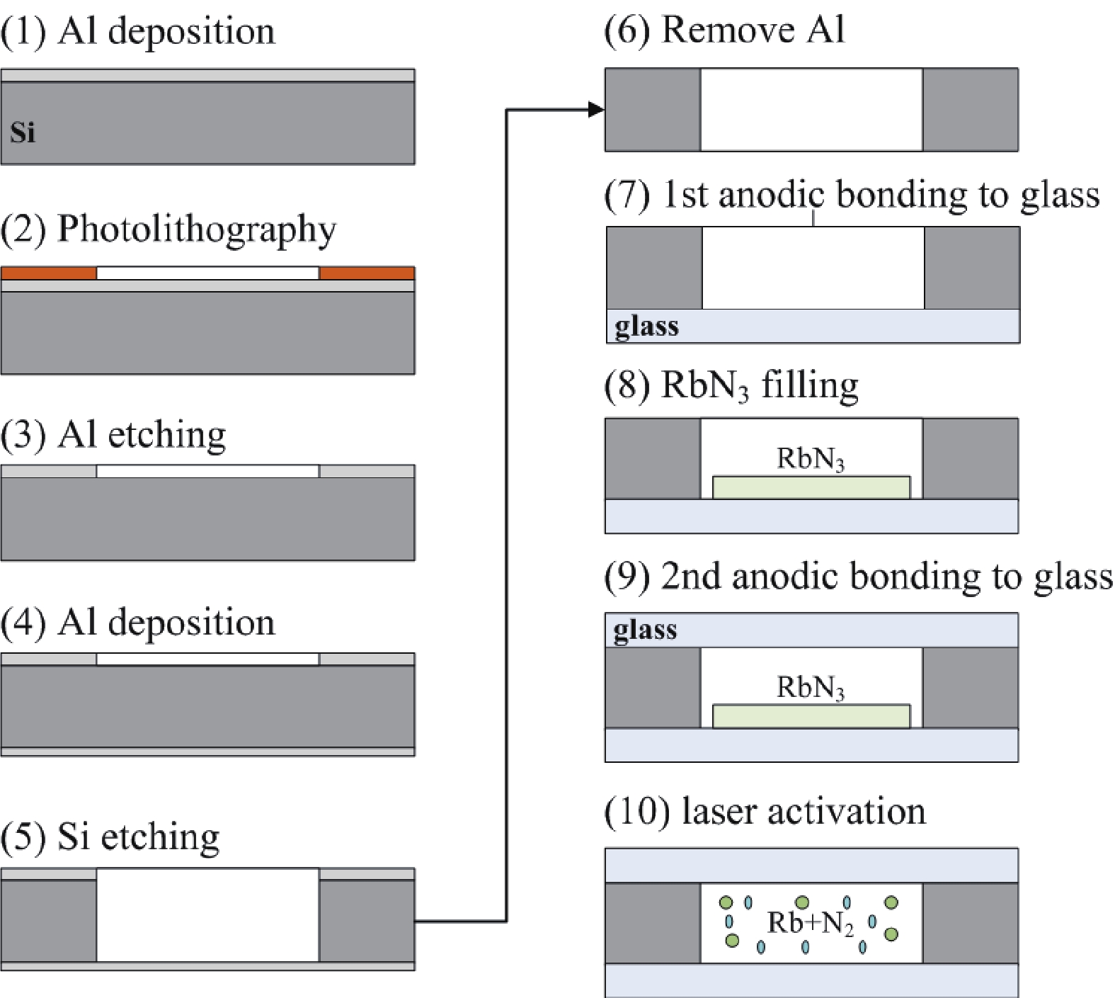
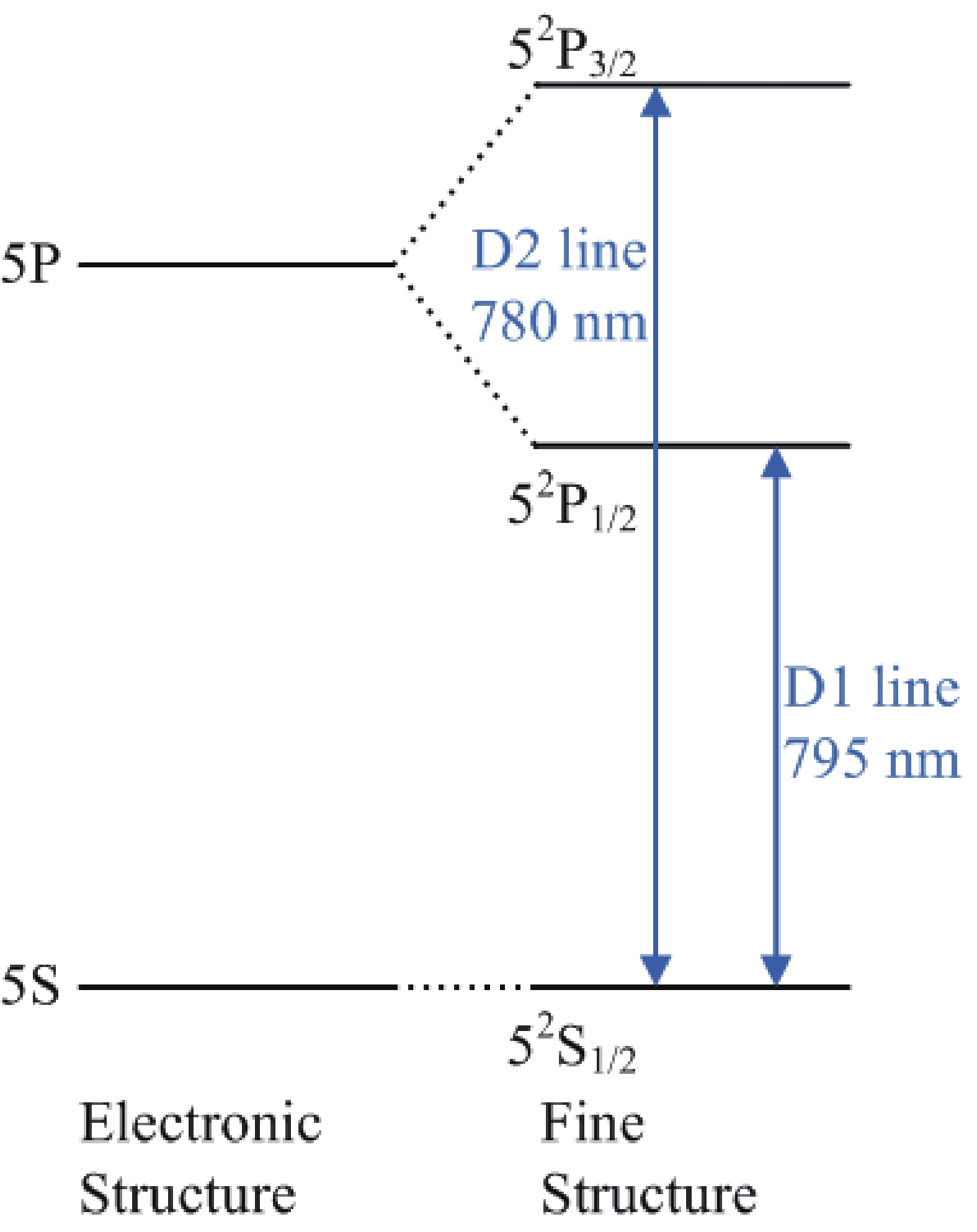
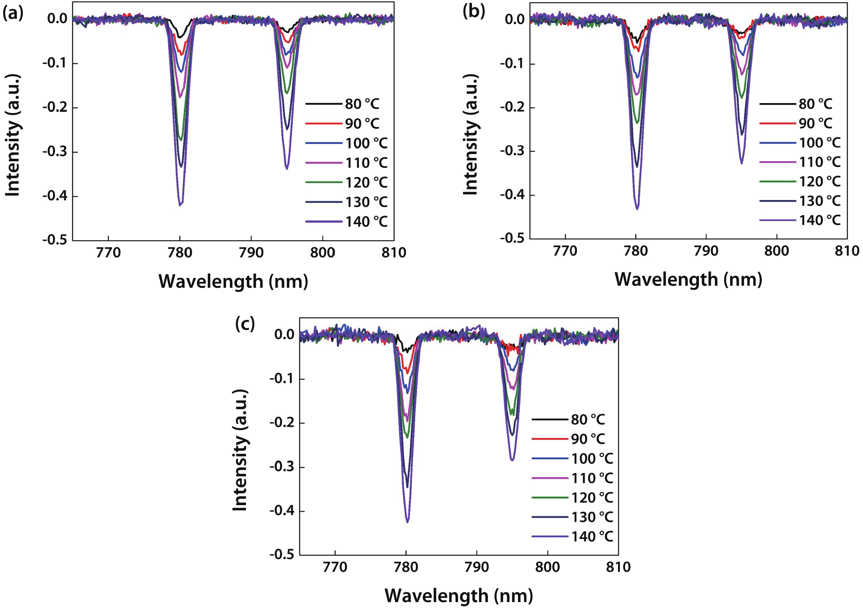
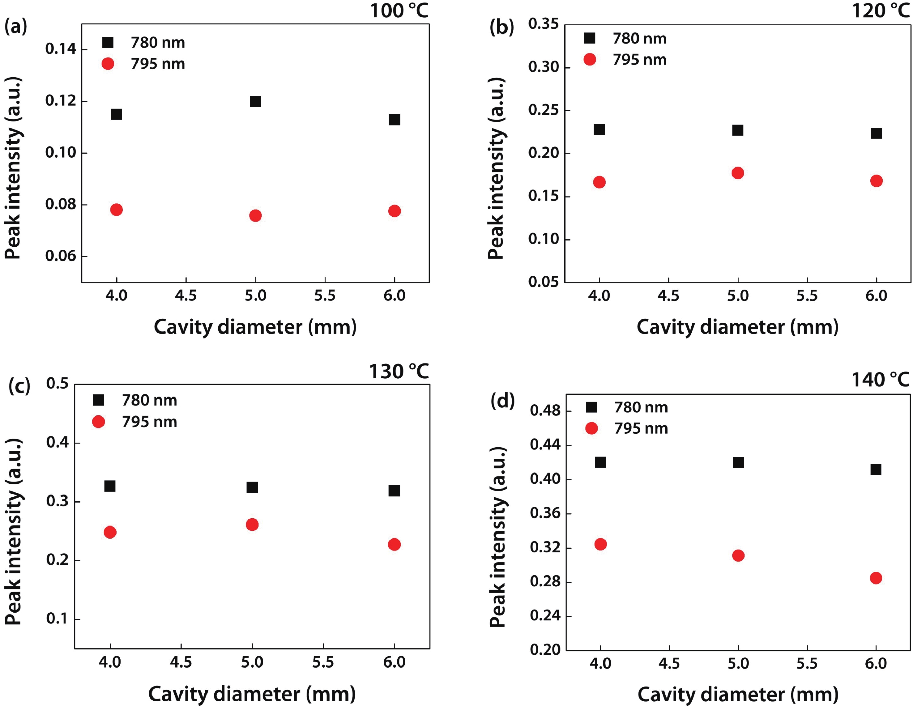
2022, 43(12): 122901 doi: 10.1088/1674-4926/43/12/122901

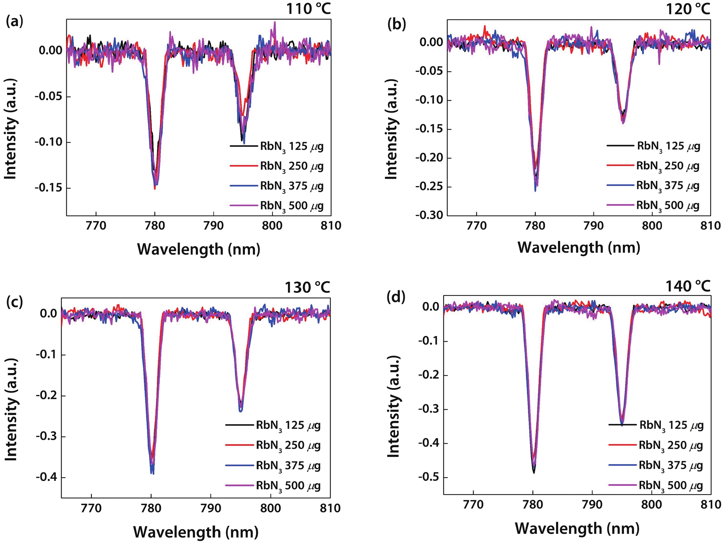
Chip-sized alkali atom vapor cells with high hermeticity are successfully fabricated through deep silicon etching and two anodic bonding processes. A self-built absorption spectrum testing system is used to test the absorption spectra of the rubidium atoms in alkali atom vapor cells. The influence of silicon cavity size, filling amount of rubidium atoms and temperature on the absorption spectra of rubidium atom vapor in the atom vapor cells are studied in depth through a theoretical analysis. This study provides a reference for the design and preparation of high quality chip-sized atom vapor cells.

J. Semicond.
2022, 43(12): 124101 doi: 10.1088/1674-4926/43/12/124101
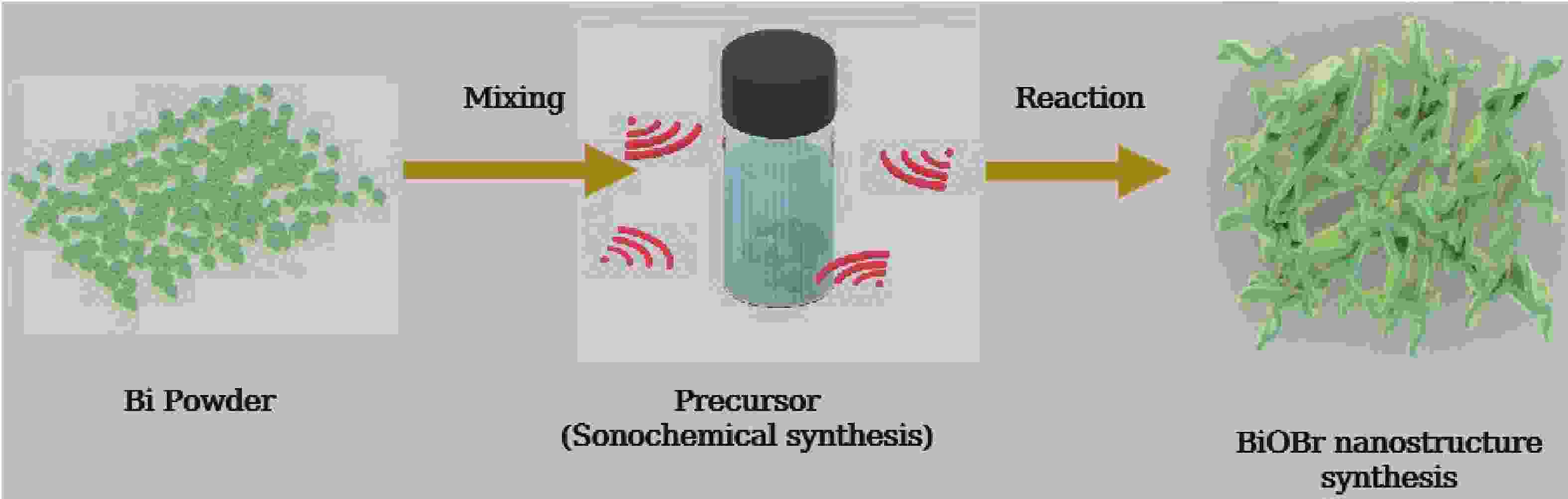
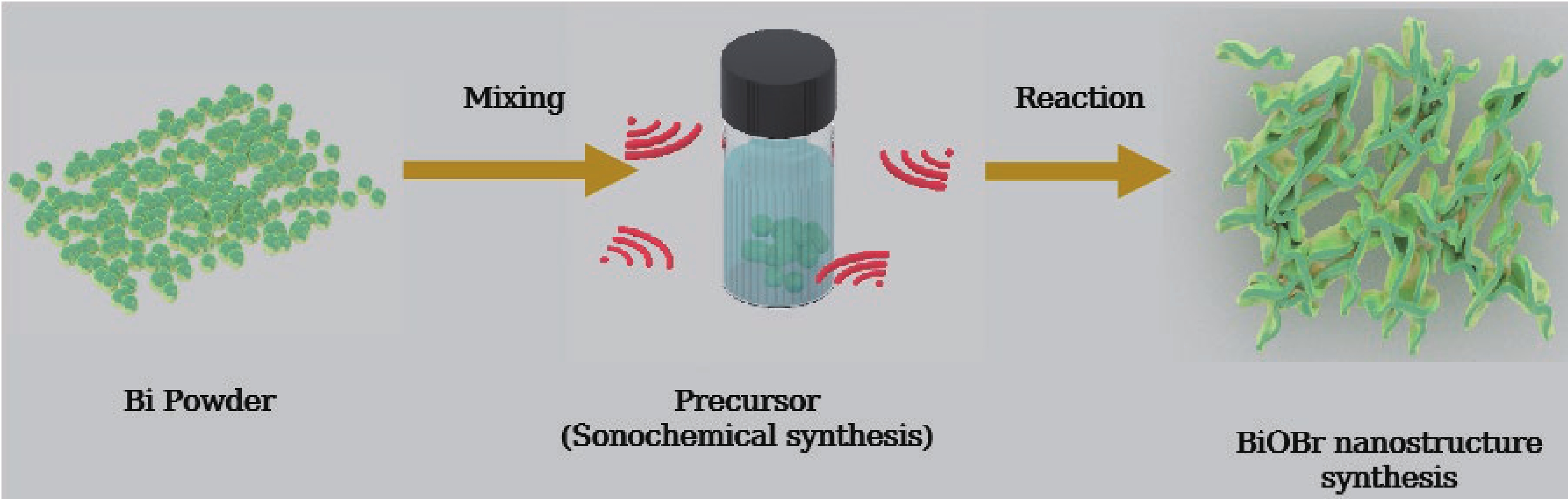
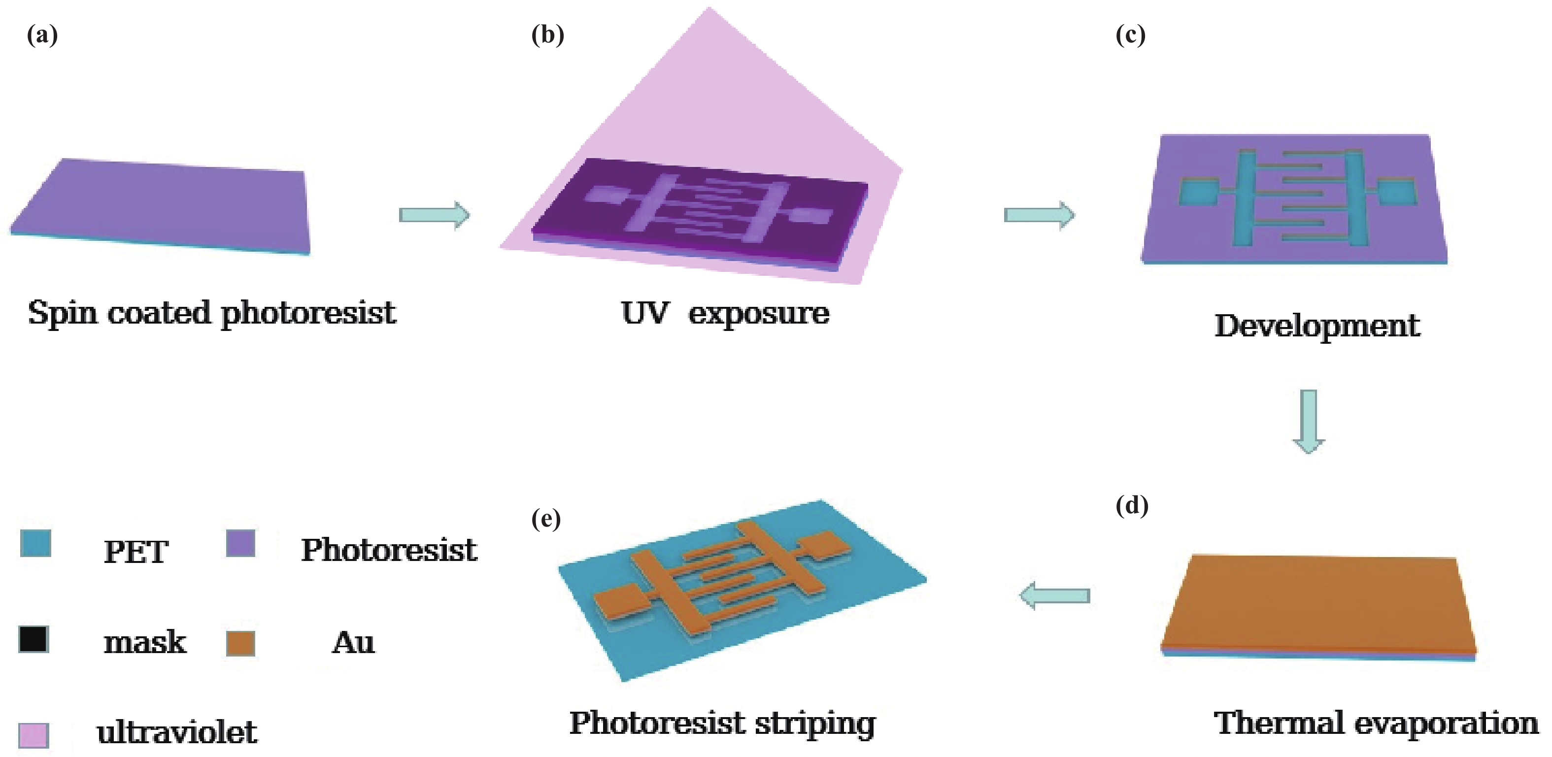
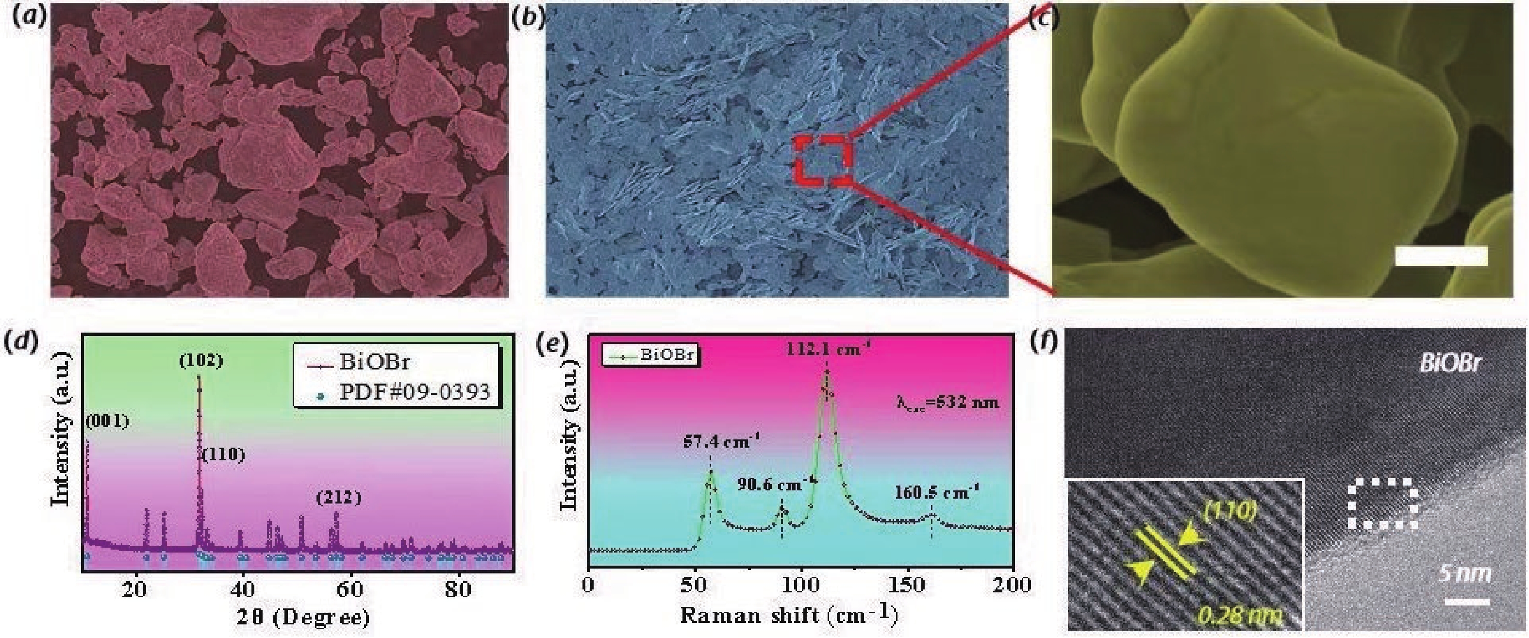
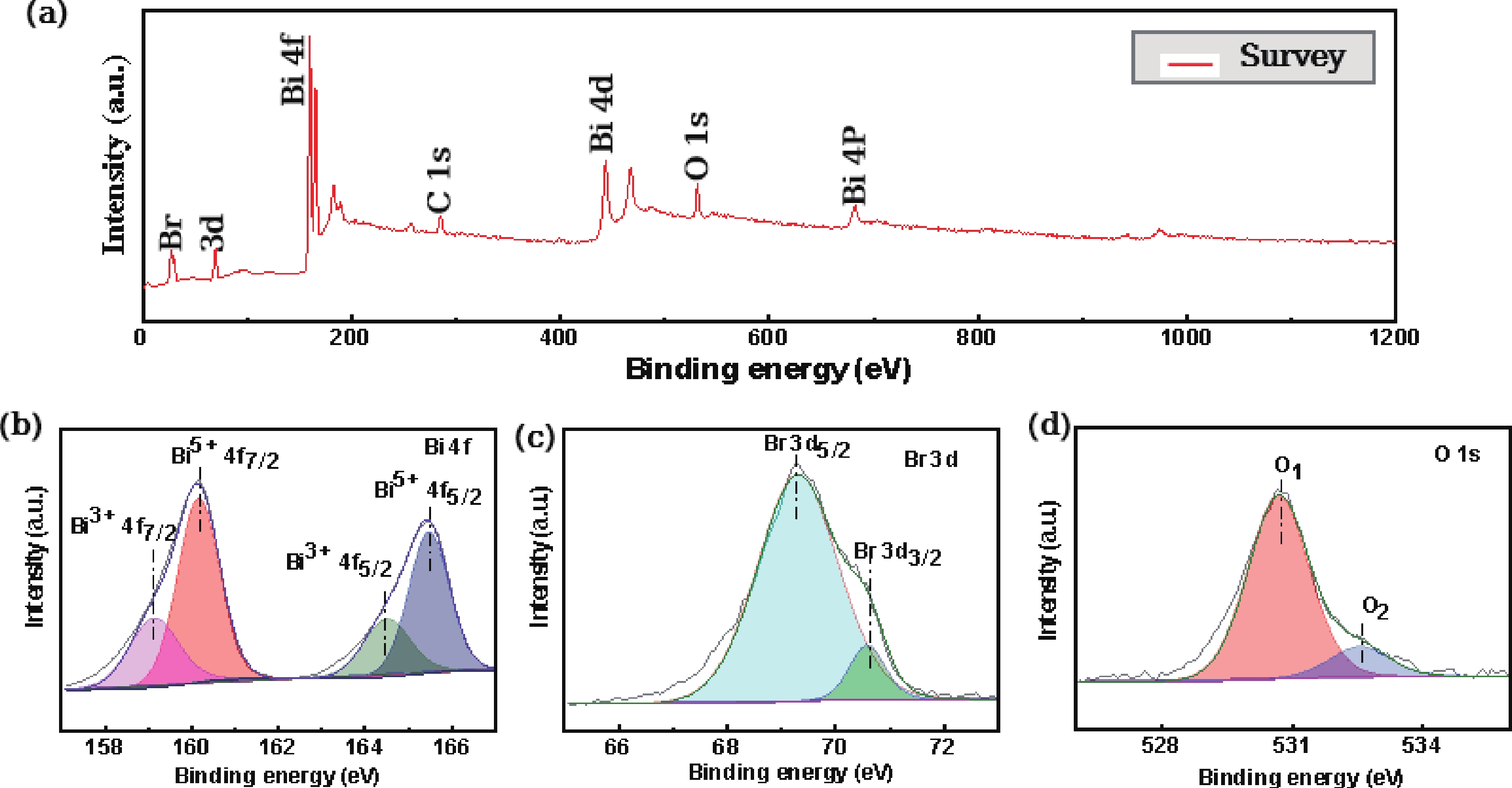
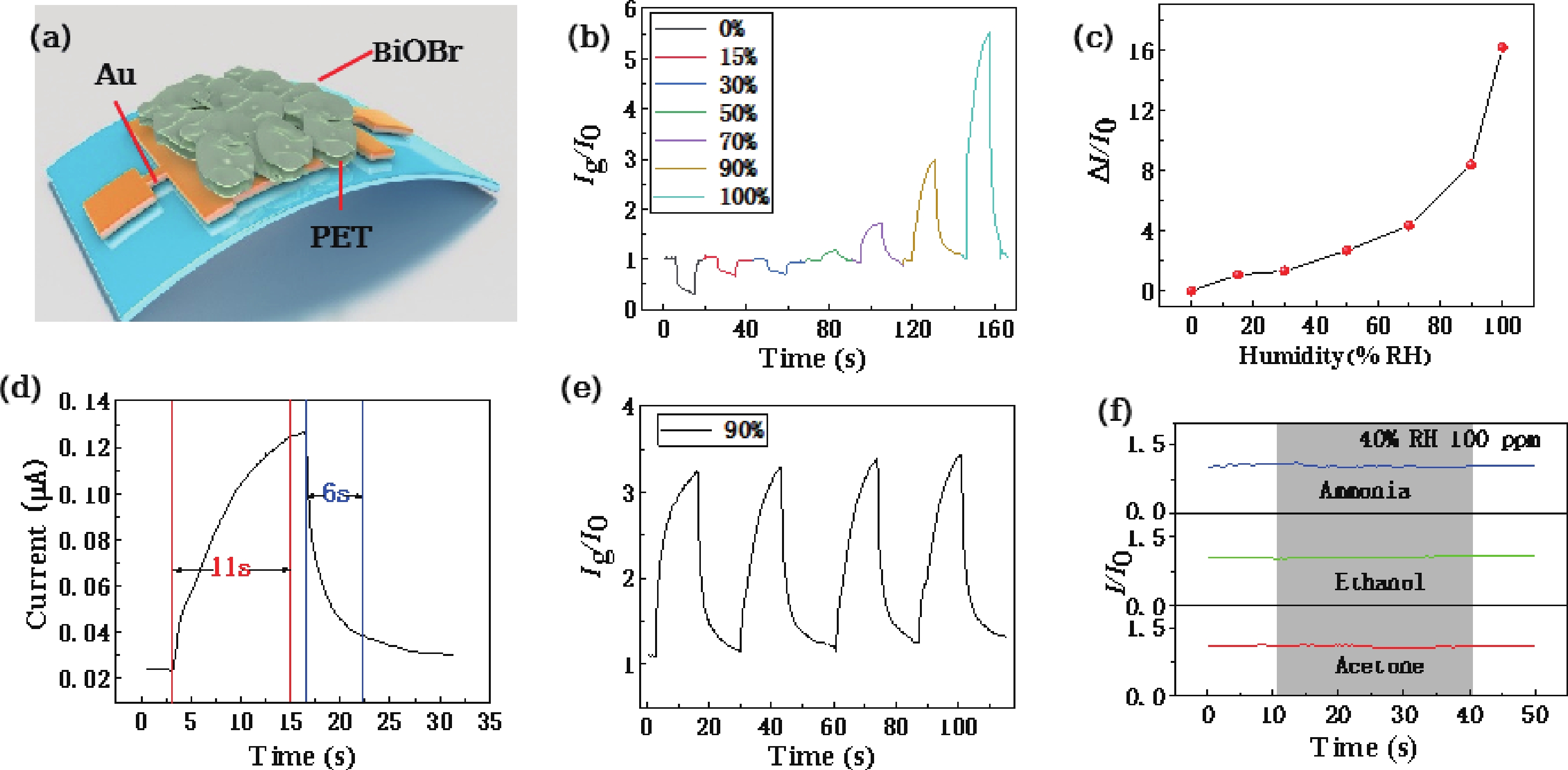
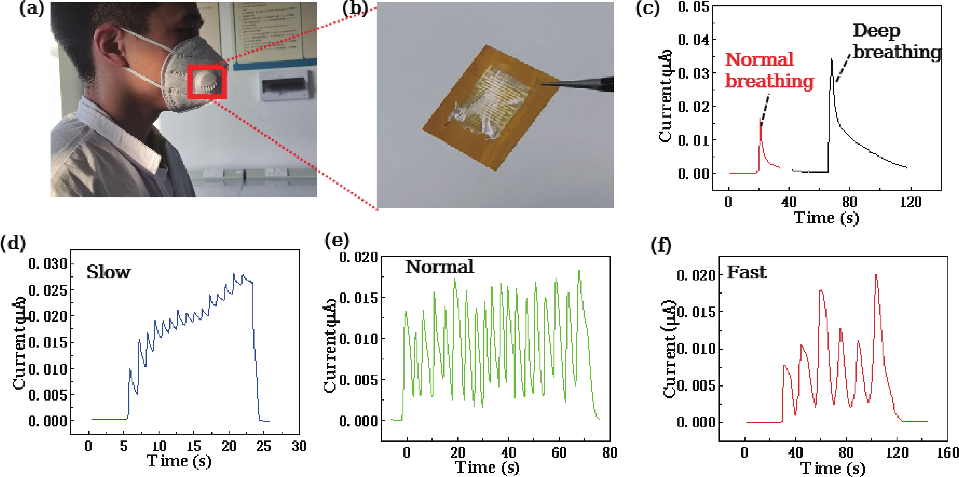
Flexible humidity sensors are effective portable devices for human respiratory monitoring. However, the current preparation of sensitive materials need harsh terms and the small production output limits their practicability. Here, we report a synthesis method of single-crystal BiOBr nanosheets under room temperature and atmospheric pressure based on a sonochemical strategy. A flexible humidity sensor enabled by BiOBr nanosheets deliver efficient sensing performance, a high humidity sensitivity (Ig/I0 = 550%) with relative humidity from 40% to 100%, an excellent selectivity, and a detection response/recovery time of 11 and 6 s, respectively. The flexible humidity sensor shows a potential application value as a wearable monitoring device for respiratory disease prevention and health monitoring.