Issue Browser
Volume 42, Issue 2,
Feb 2021

J. Semicond.
2021, 42(2): 023101 doi: 10.1088/1674-4926/42/2/023101
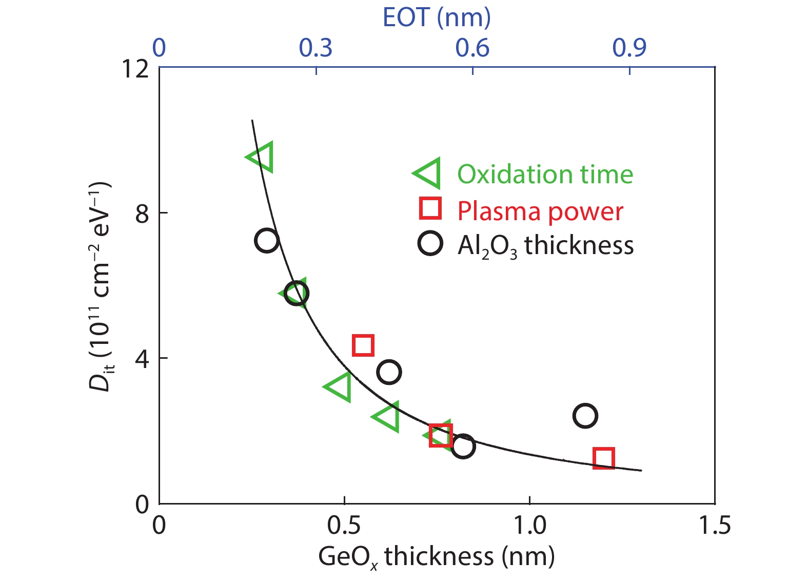
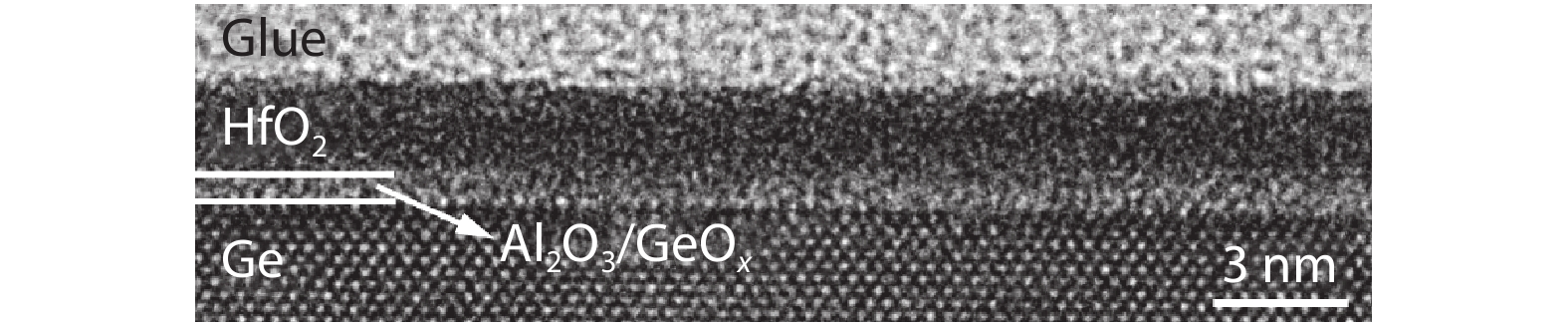
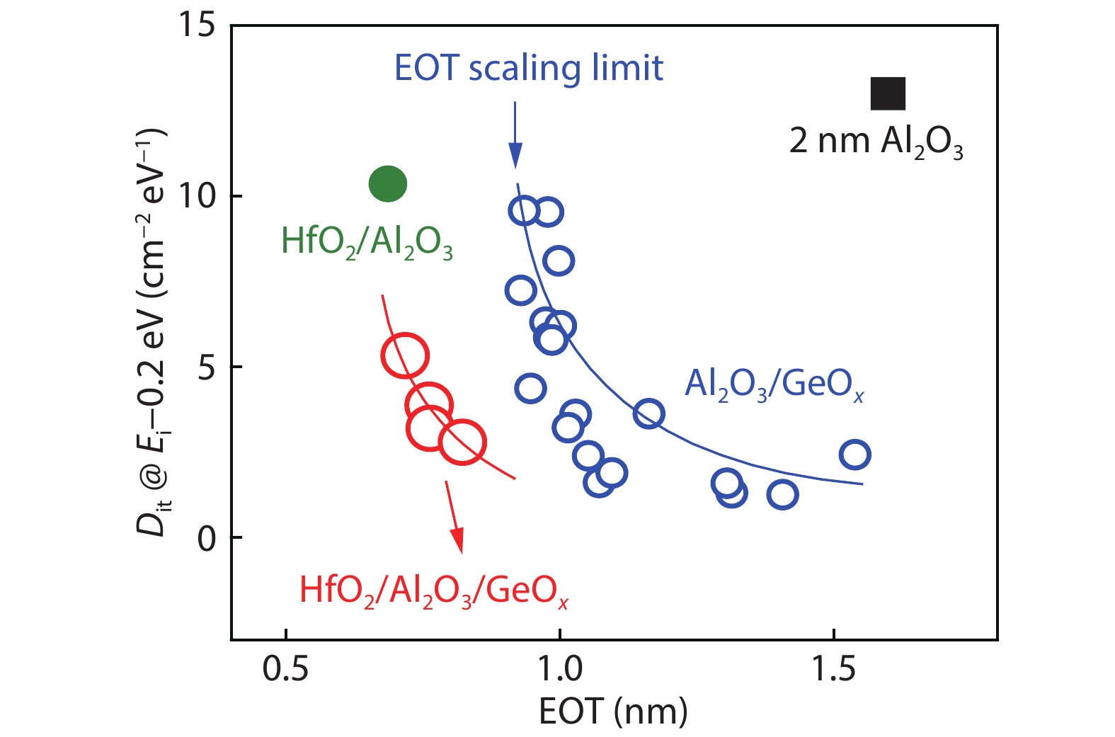
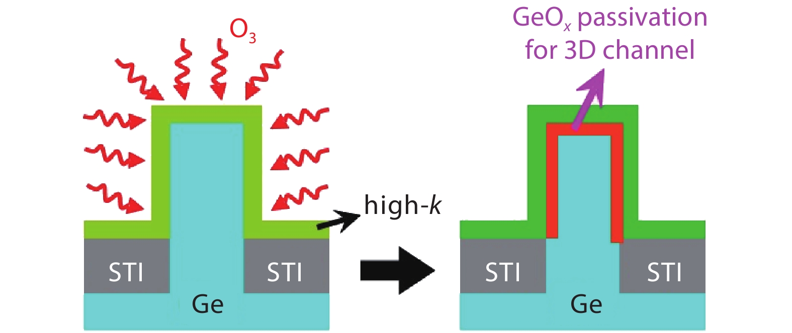
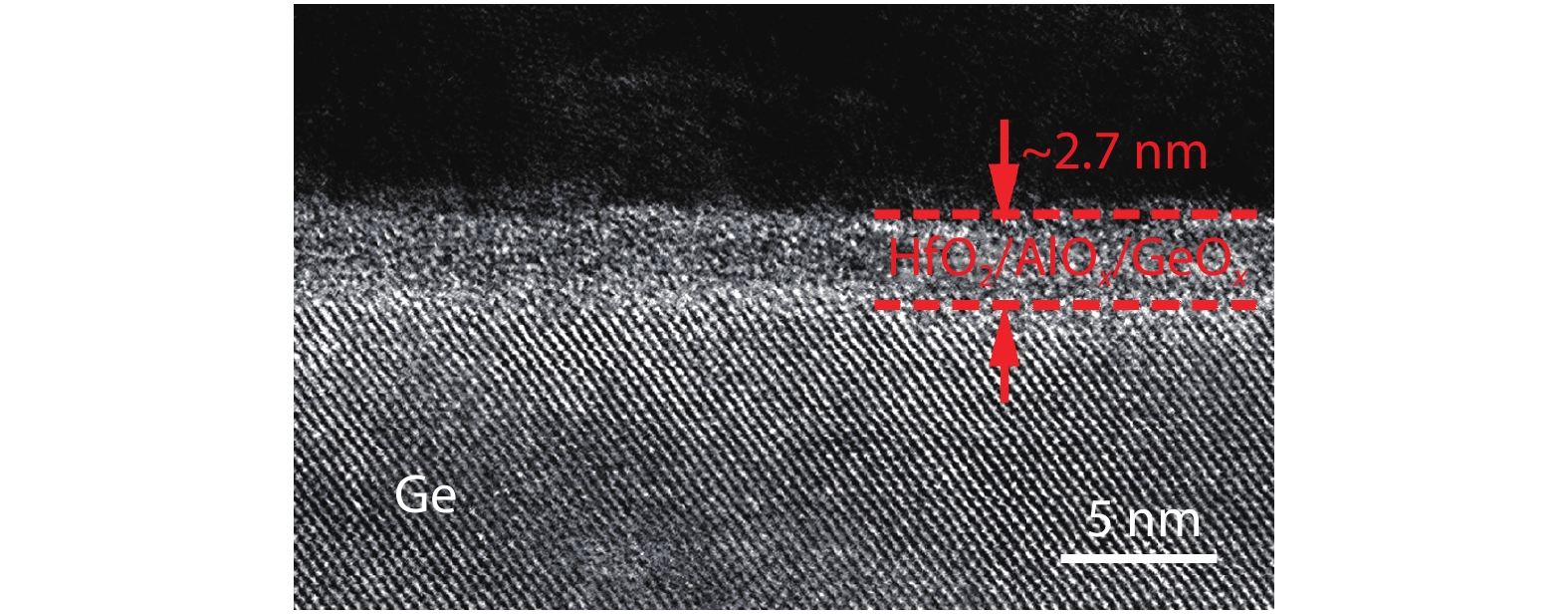
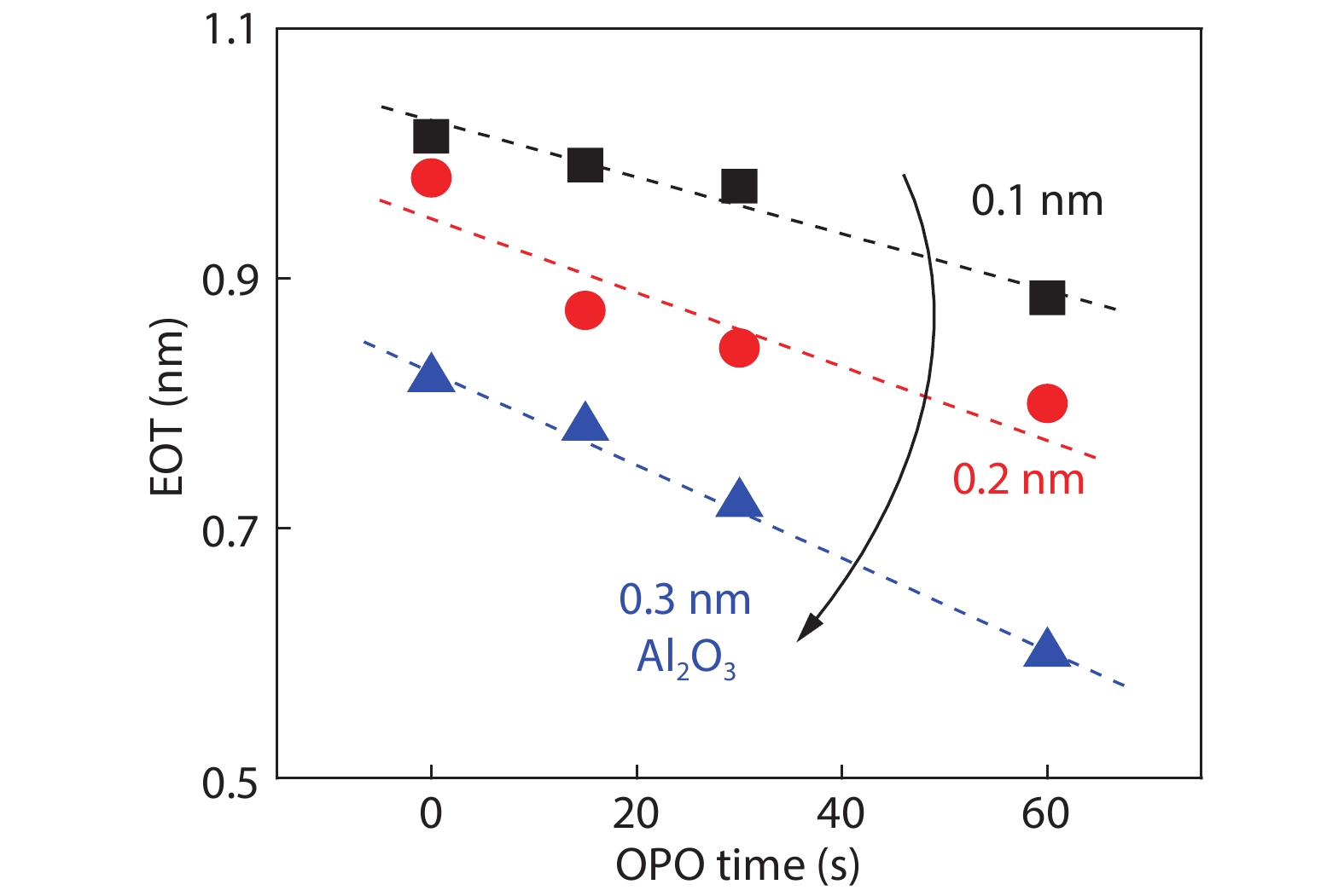
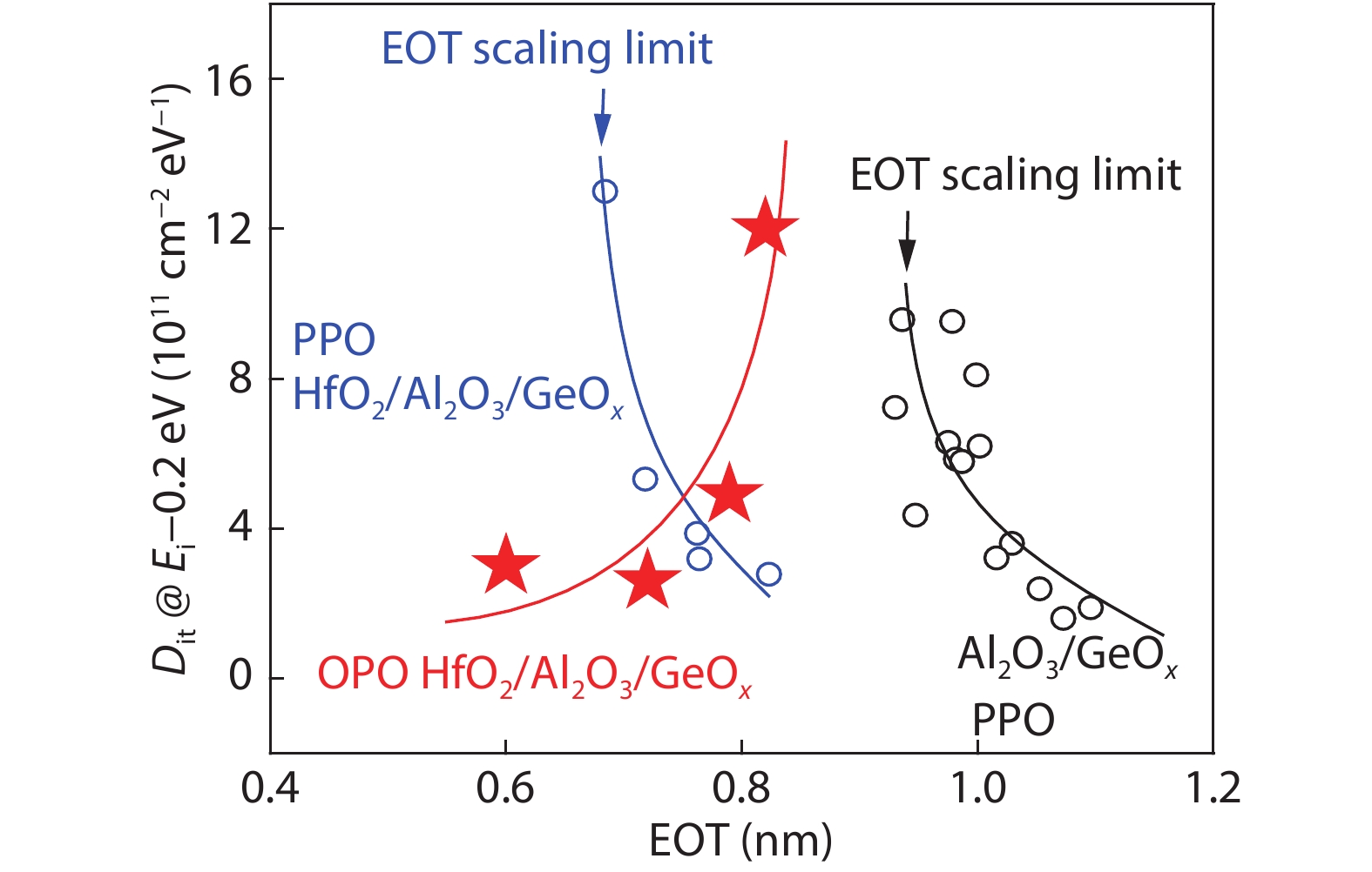
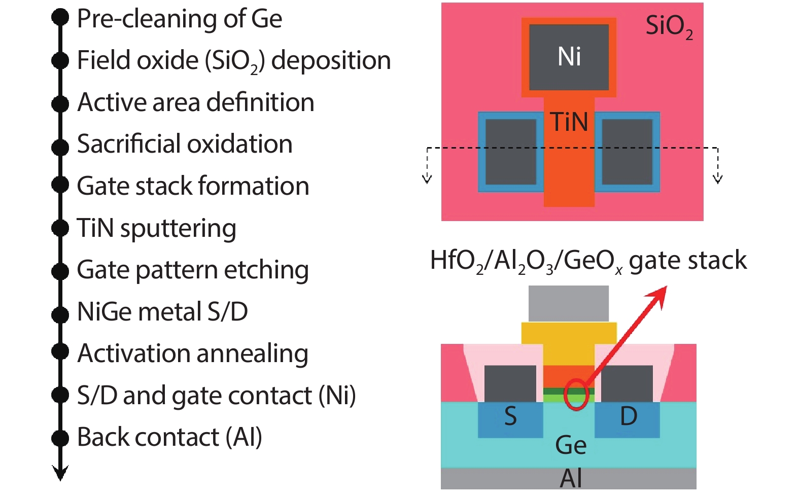
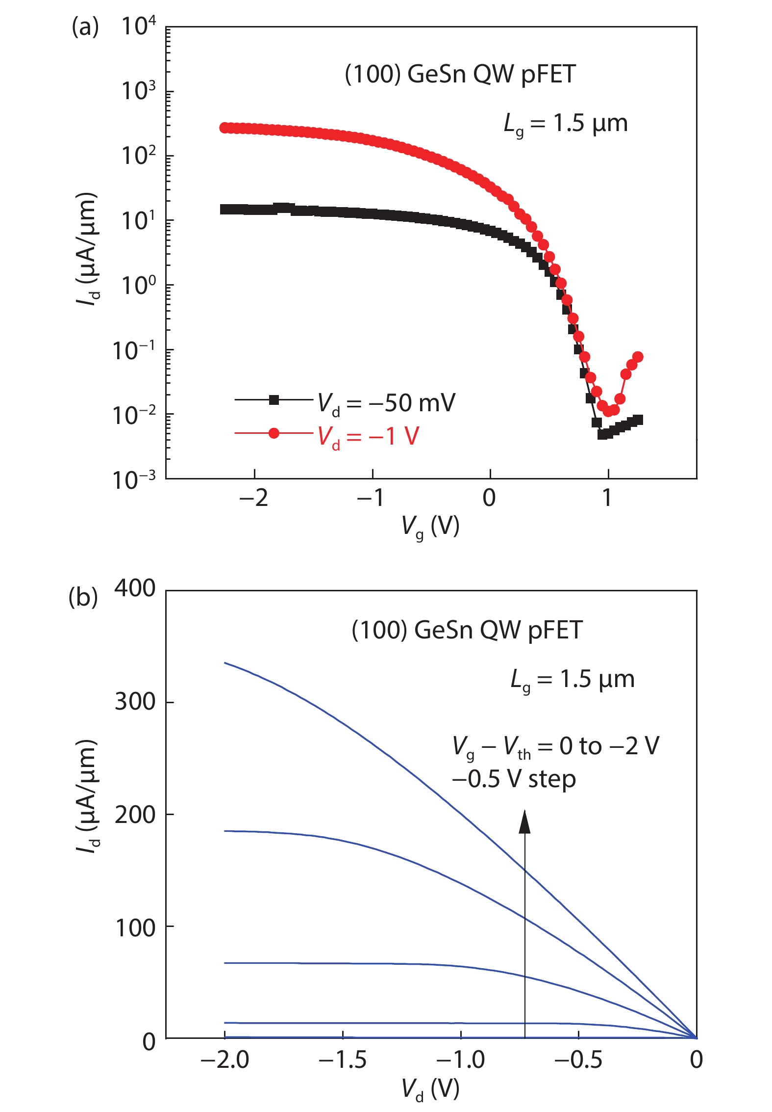
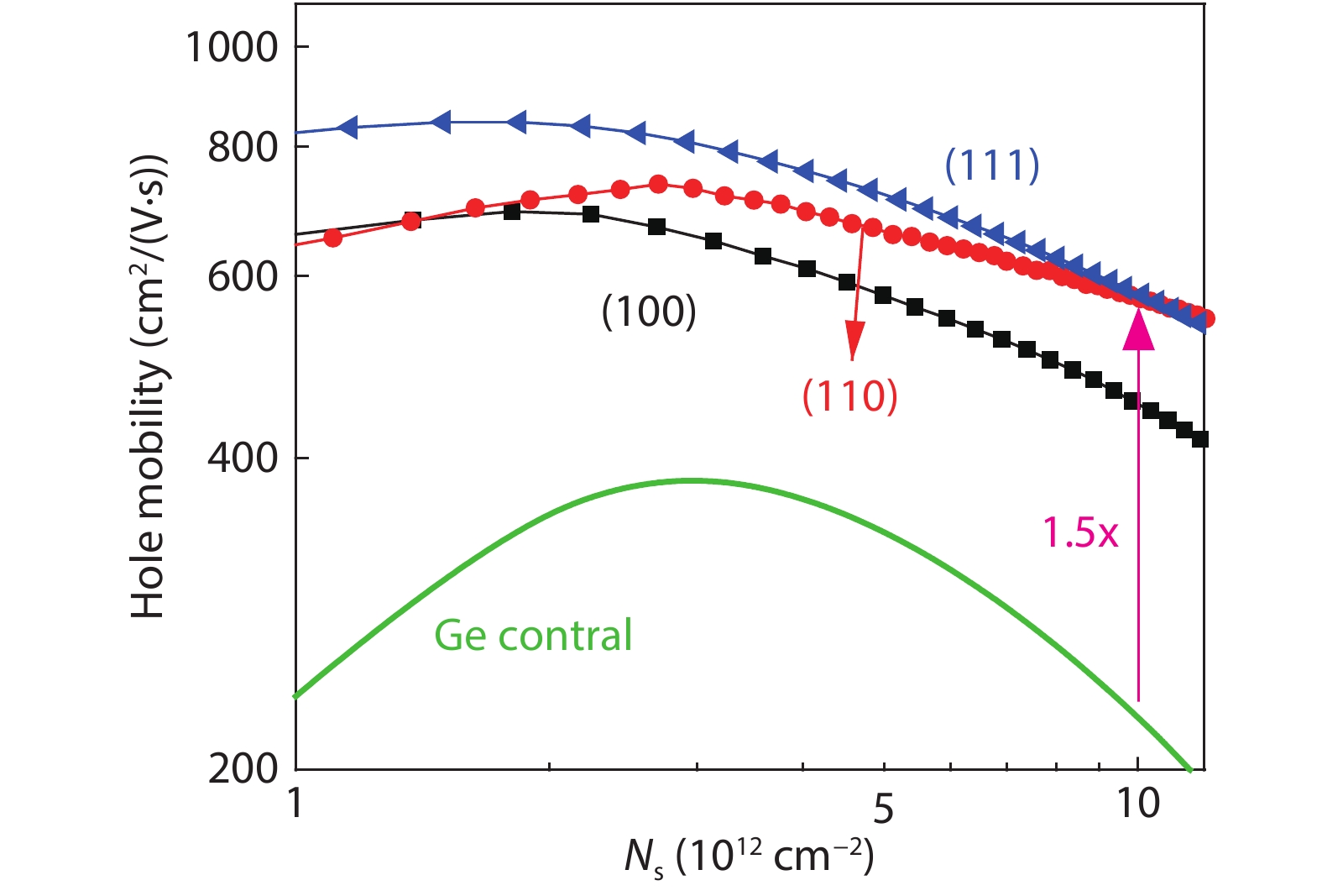
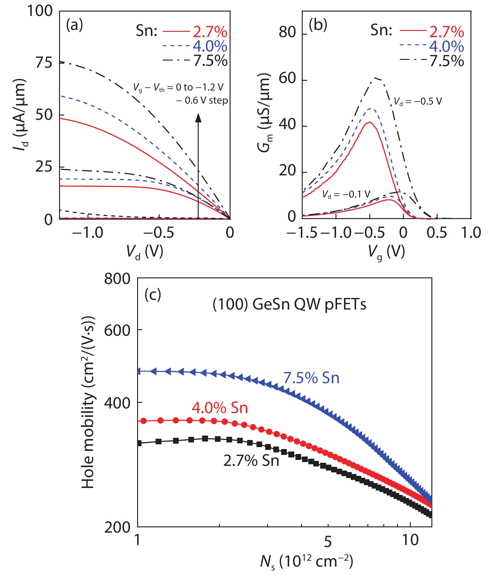
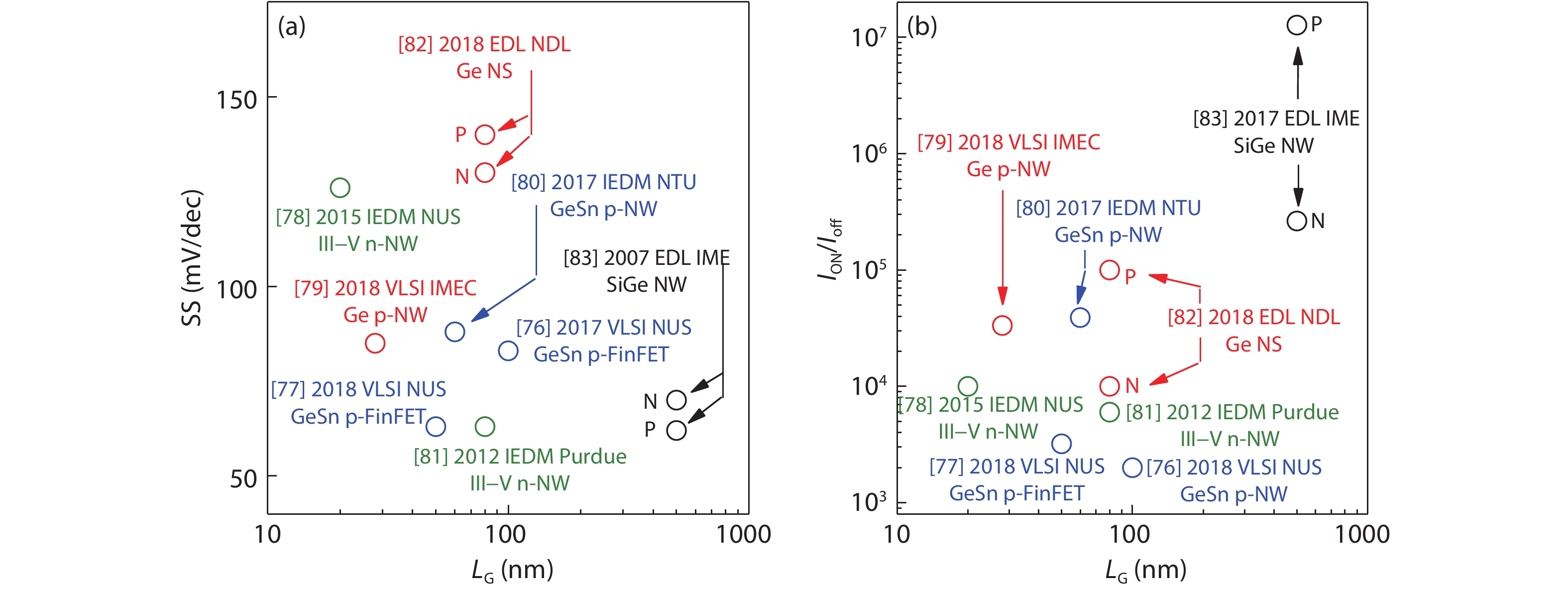
The performance enhancement of conventional Si MOSFETs through device scaling is becoming increasingly difficult. The application of high mobility channel materials is one of the most promising solutions to overcome the bottleneck. The Ge and GeSn channels attract a lot of interest as the alternative channel materials, not only because of the high carrier mobility but also the superior compatibility with typical Si CMOS technology. In this paper, the recent progress of high mobility Ge and GeSn MOSFETs has been investigated, providing feasible approaches to improve the performance of Ge and GeSn devices for future CMOS technologies.


J. Semicond.
2021, 42(2): 023102 doi: 10.1088/1674-4926/42/2/023102

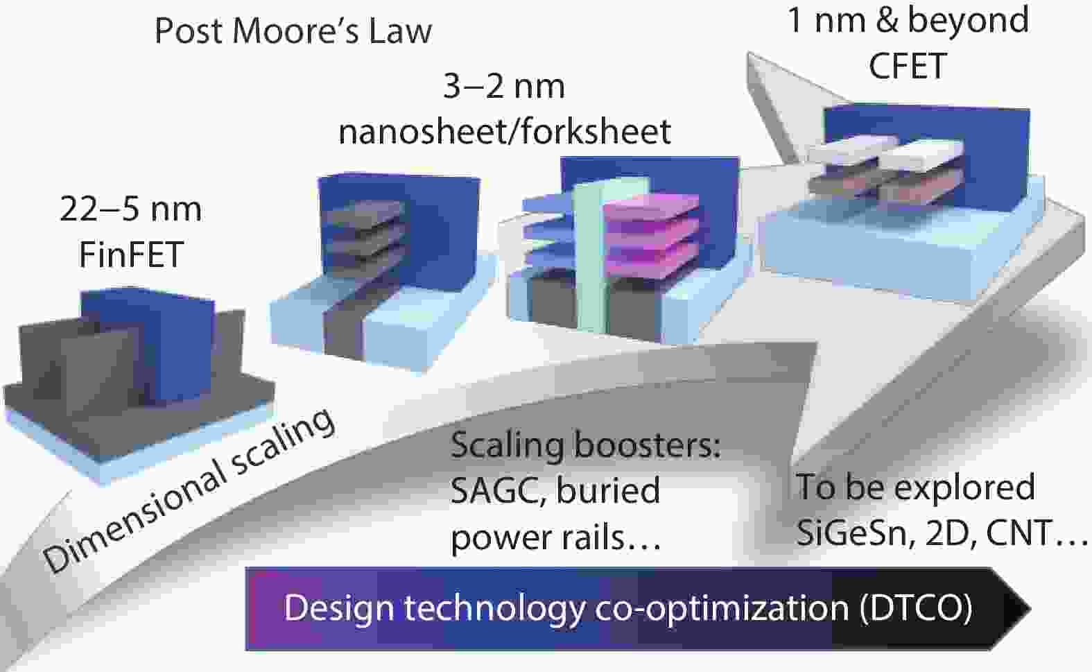
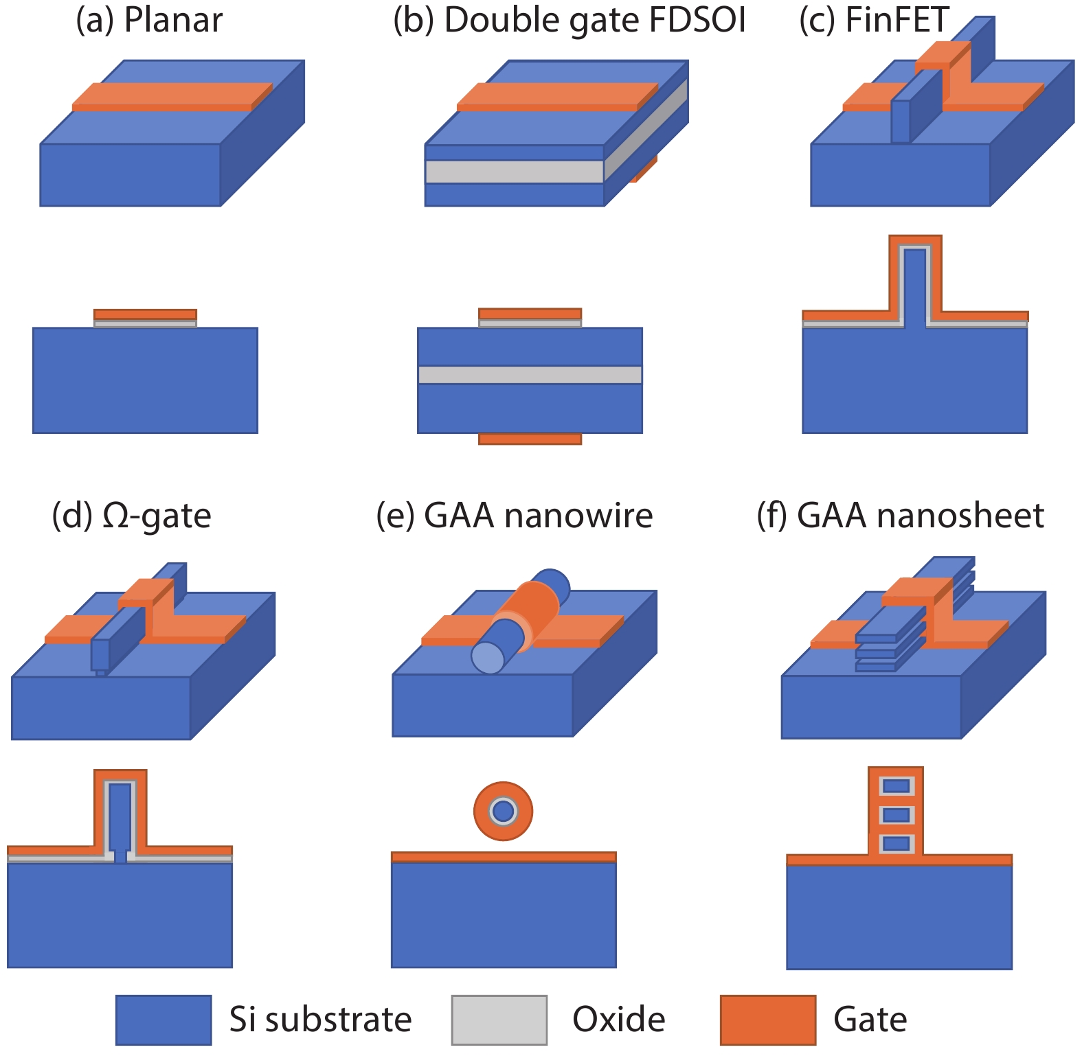
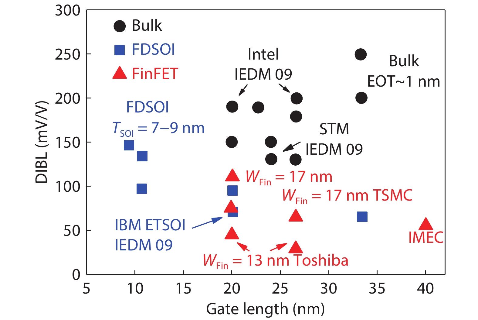
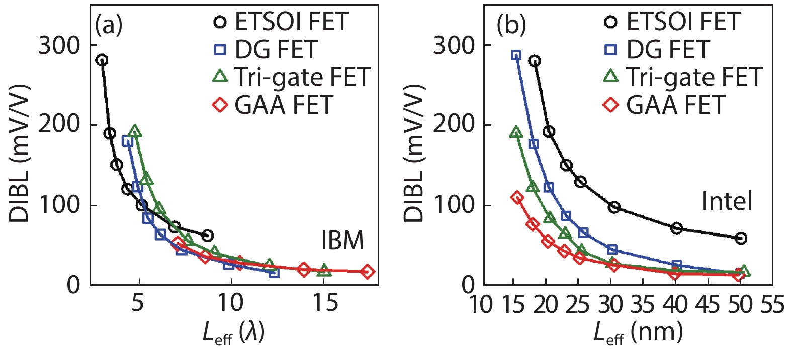
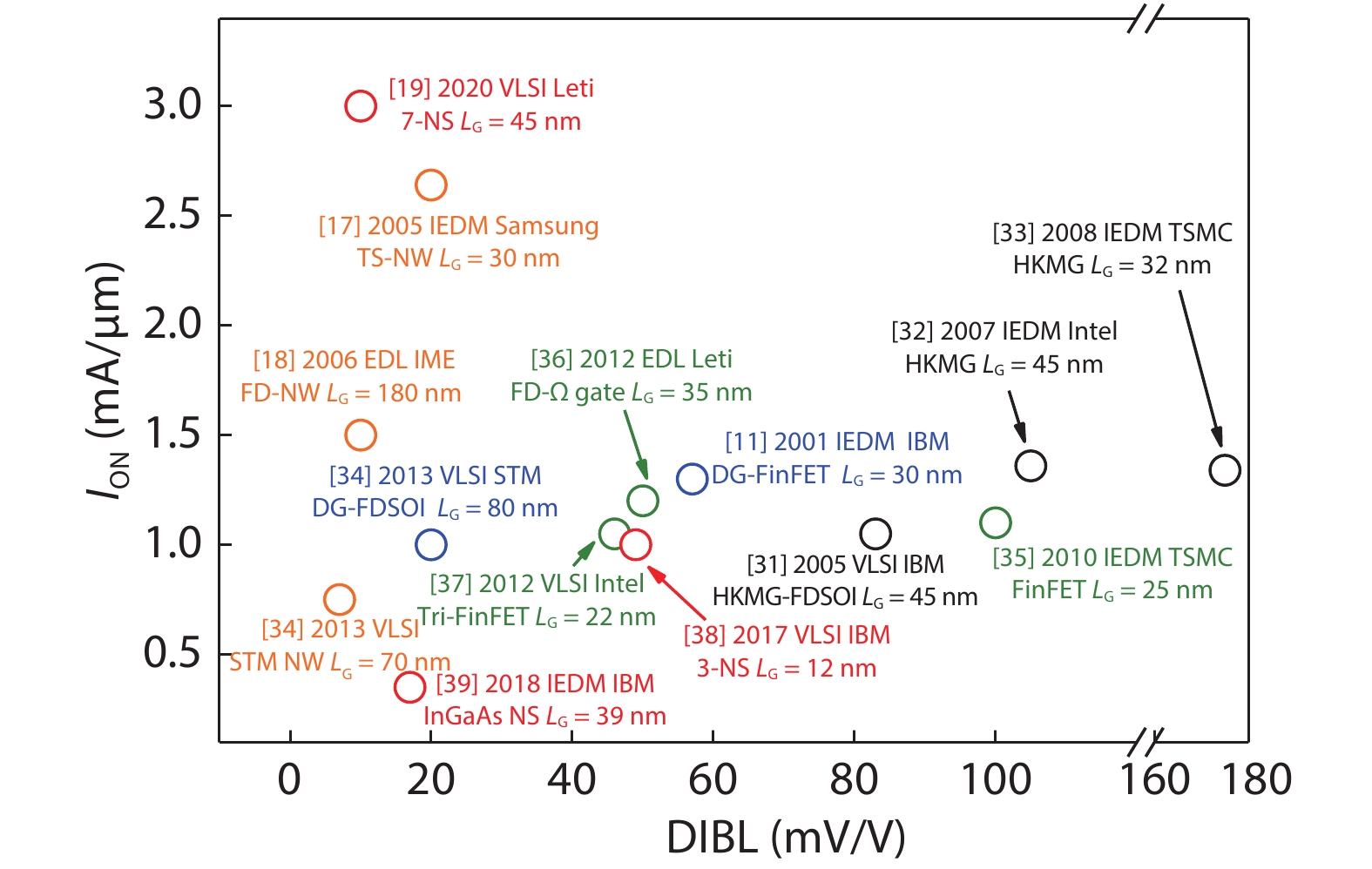
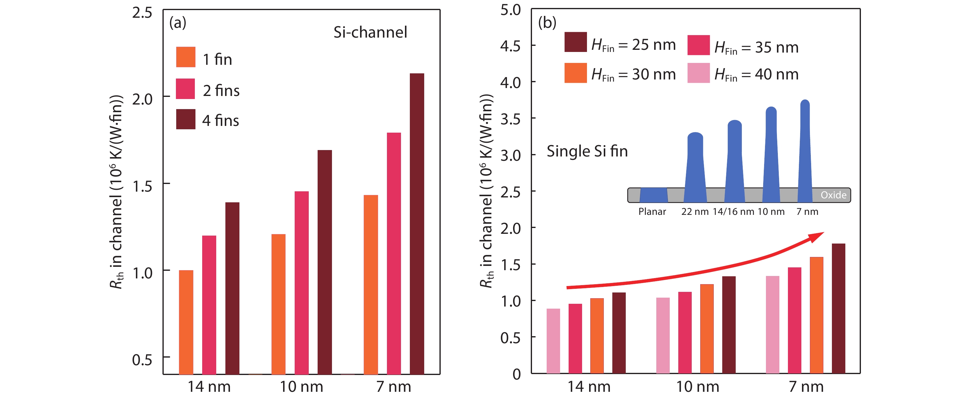
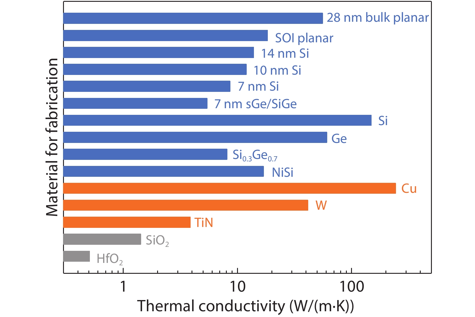
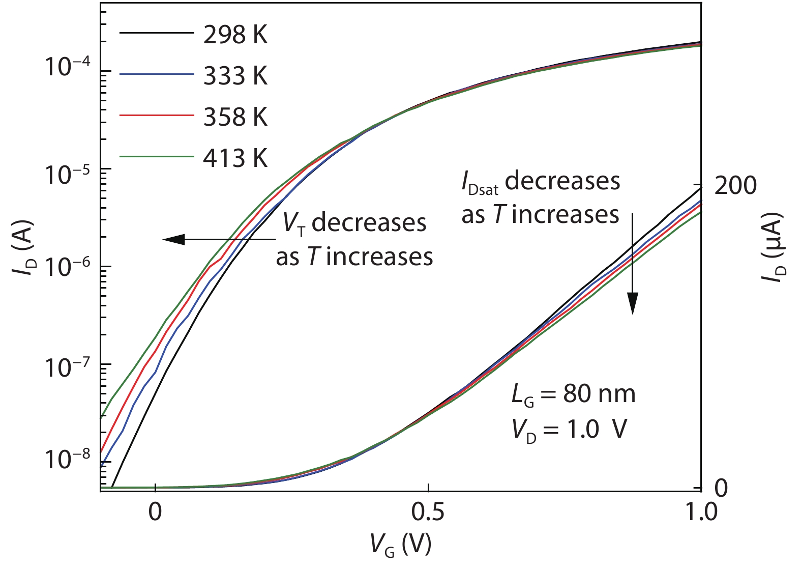
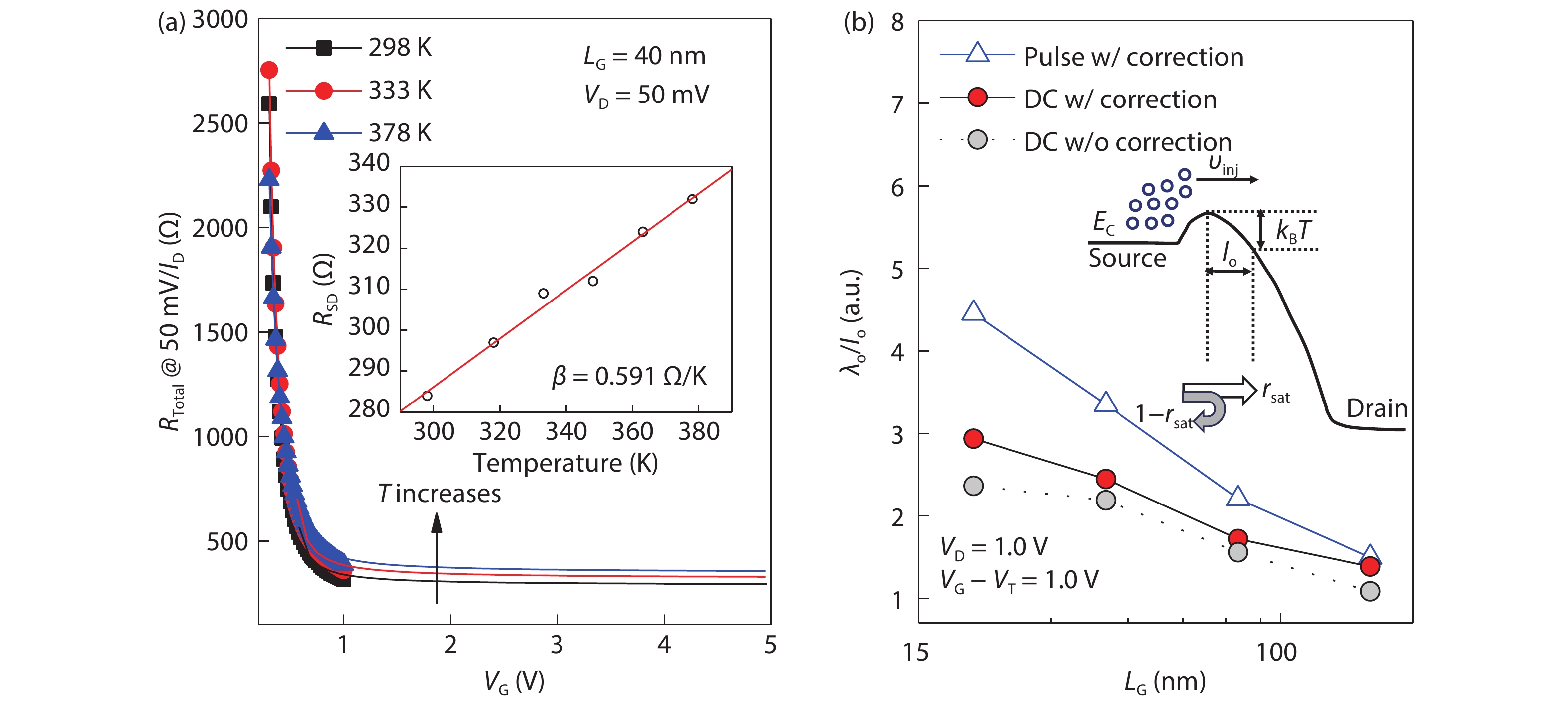
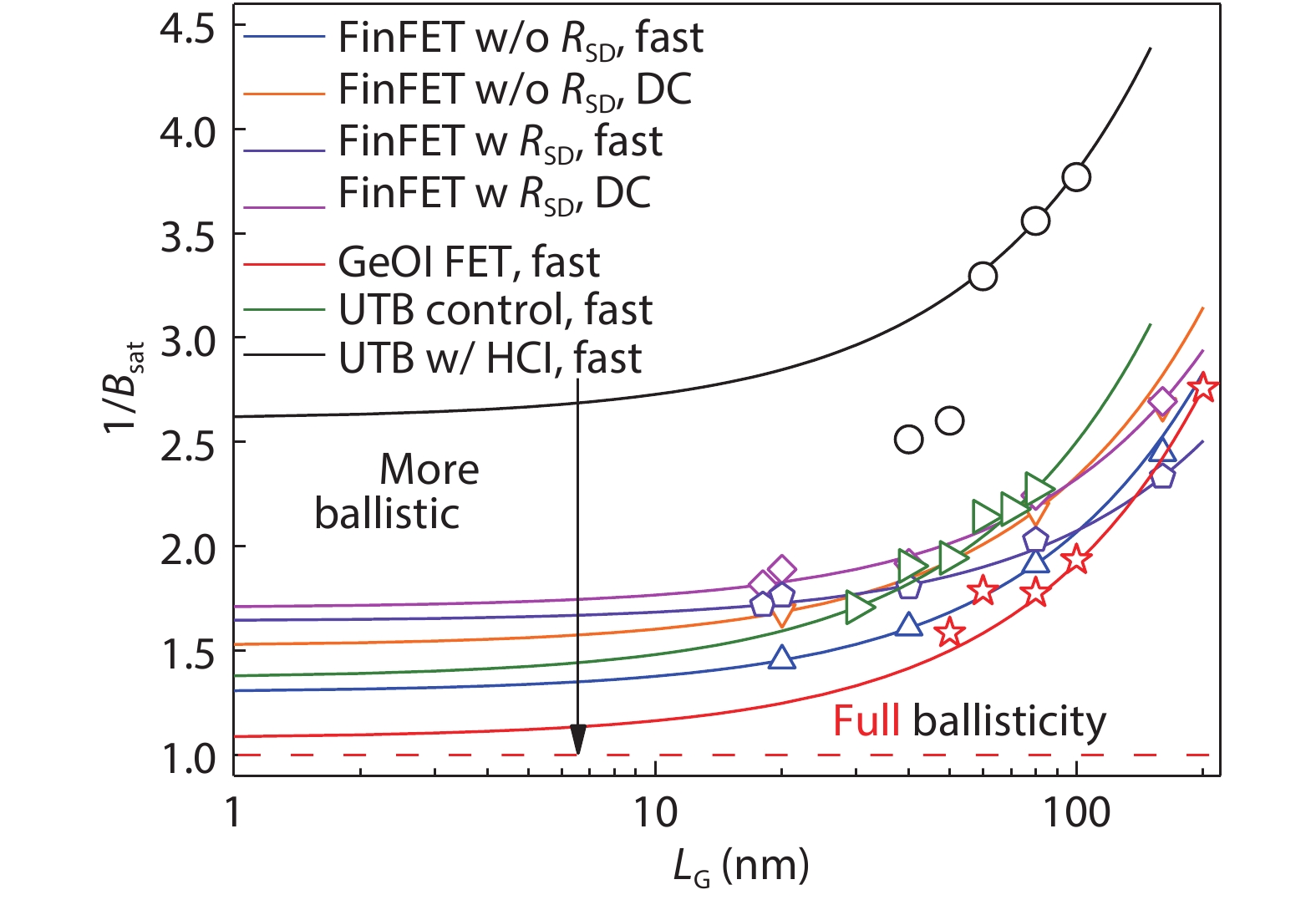
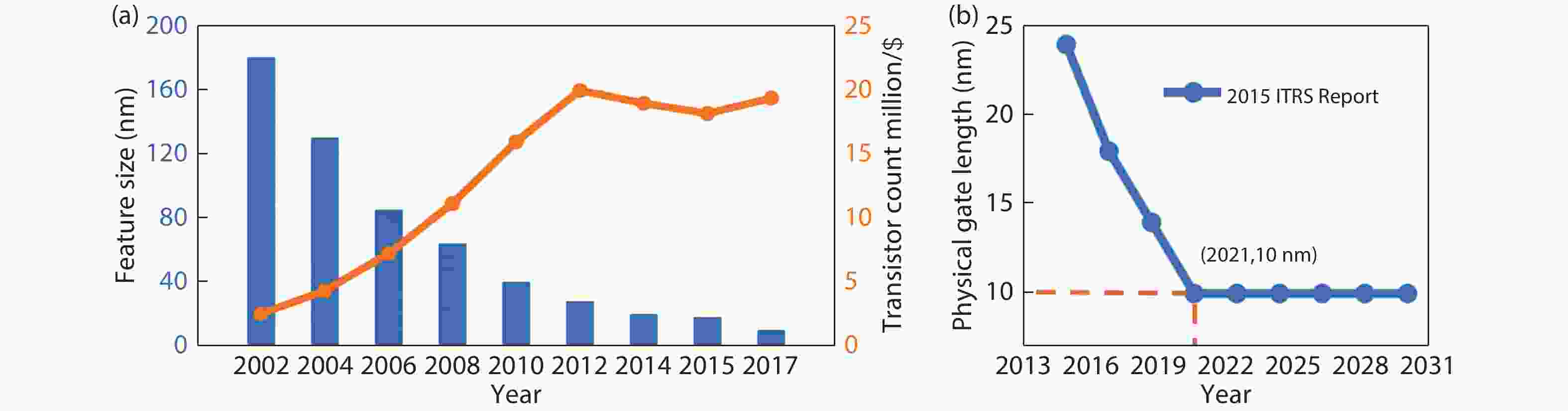
This work reviews the state-of-the art multi-gate field-effect transistor (MuGFET) process technologies and compares the device performance and reliability characteristics of the MuGFETs with the planar Si CMOS devices. Owing to the 3D wrapped gate structure, MuGFETs can suppress the SCEs and improve the ON-current performance due to the volume inversion of the channel region. As the Si CMOS technology pioneers to sub-10 nm nodes, the process challenges in terms of lithography capability, process integration controversies, performance variability etc. were also discussed in this work. Due to the severe self-heating effect in the MuGFETs, the ballistic transport and reliability characteristics were investigated. Future alternatives for the current Si MuGFET technology were discussed at the end of the paper. More work needs to be done to realize novel high mobility channel MuGFETs with better performance and reliability.


J. Semicond.
2021, 42(2): 023103 doi: 10.1088/1674-4926/42/2/023103
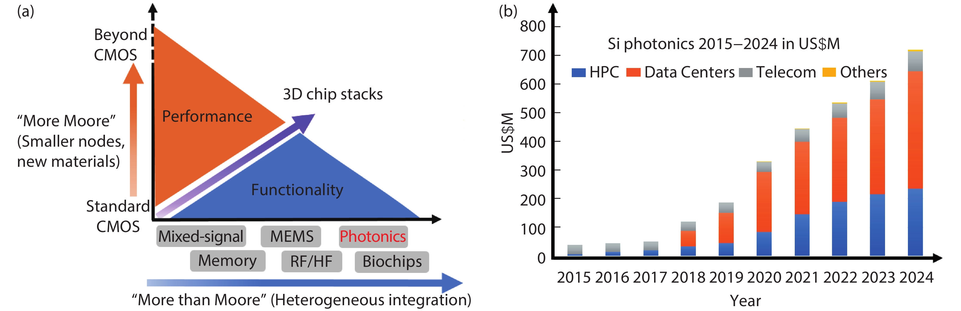
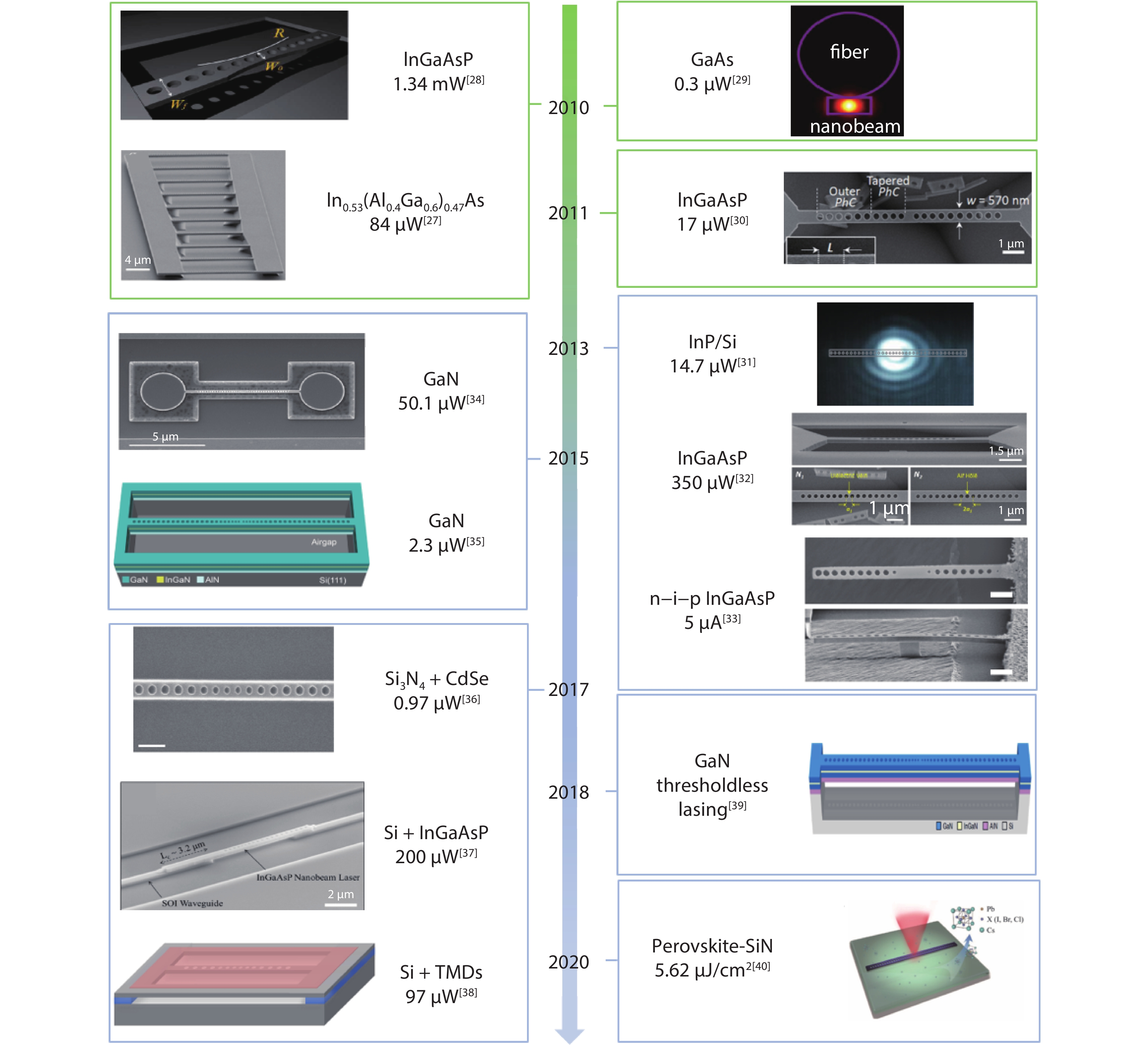
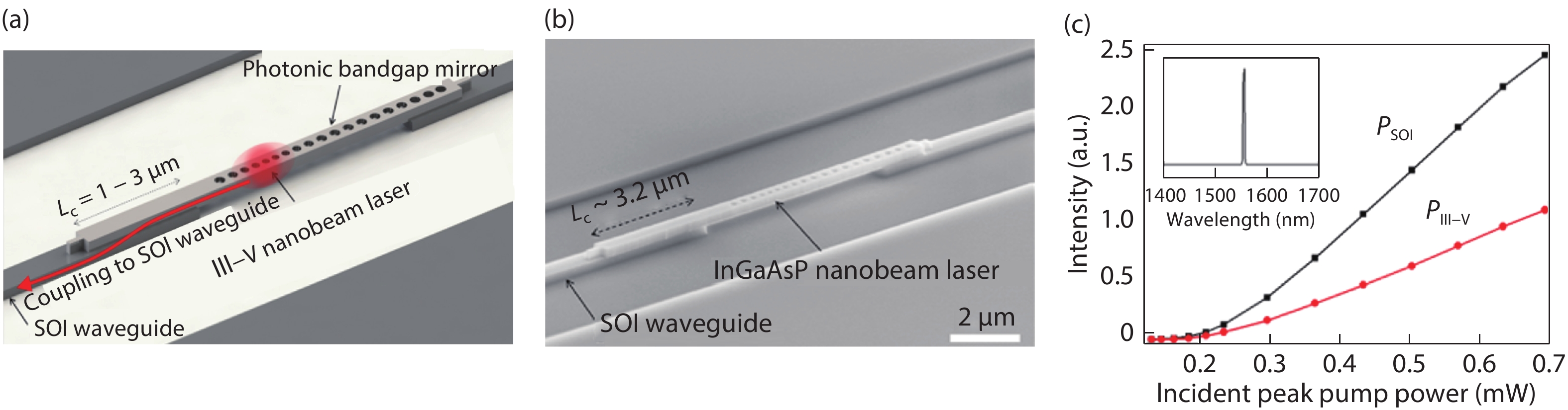
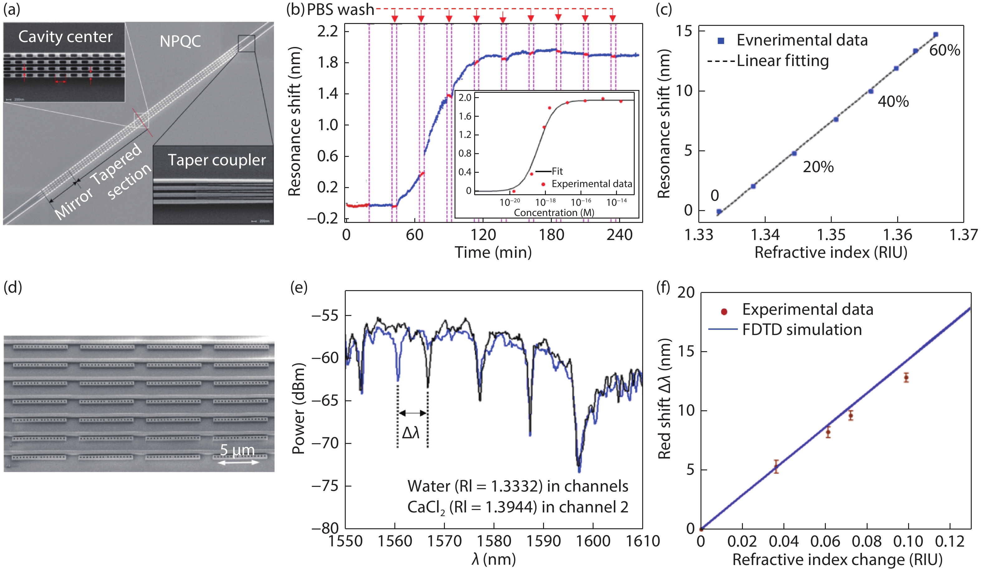
Integrated circuit (IC) industry has fully considered the fact that the Moore’s Law is slowing down or ending. Alternative solutions are highly and urgently desired to break the physical size limits in the More-than-Moore era. Integrated silicon photonics technology exhibits distinguished potential to achieve faster operation speed, less power dissipation, and lower cost in IC industry, because their COMS compatibility, fast response, and high monolithic integration capability. Particularly, compared with other on-chip resonators (e.g. microrings, 2D photonic crystal cavities) silicon-on-insulator (SOI)-based photonic crystal nanobeam cavity (PCNC) has emerged as a promising platform for on-chip integration, due to their attractive properties of ultra-high Q/V, ultra-compact footprints and convenient integration with silicon bus-waveguides. In this paper, we present a comprehensive review on recent progress of on-chip PCNC devices for lasing, modulation, switching/filting and label-free sensing, etc.


J. Semicond.
2021, 42(2): 023104 doi: 10.1088/1674-4926/42/2/023104
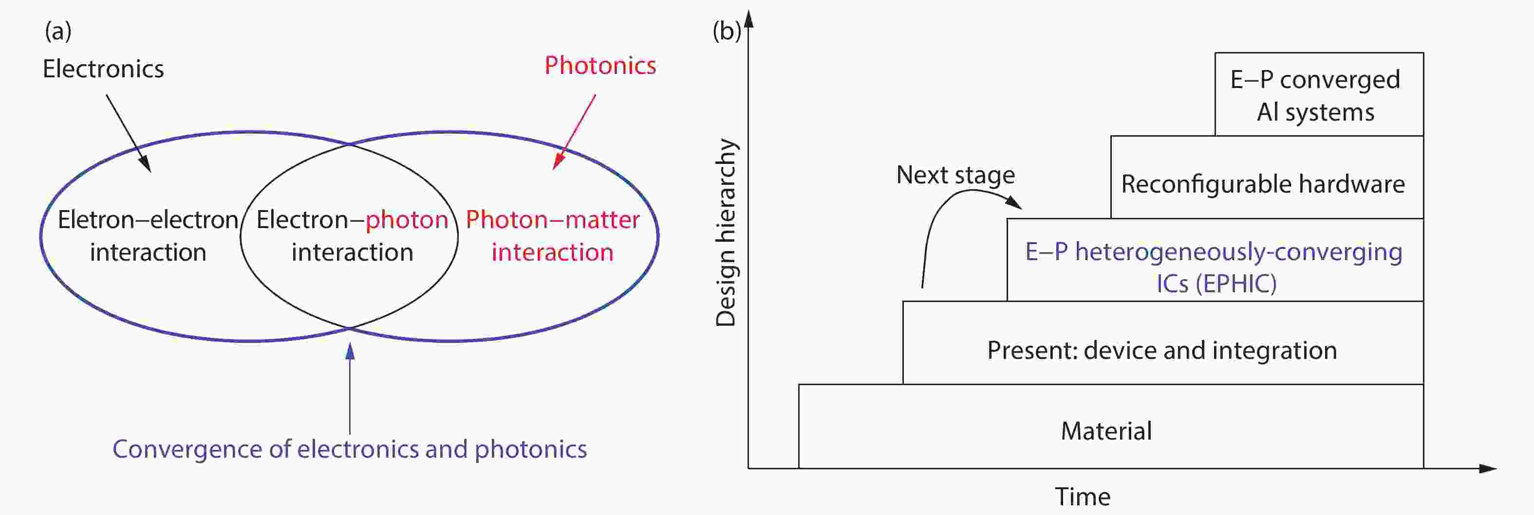
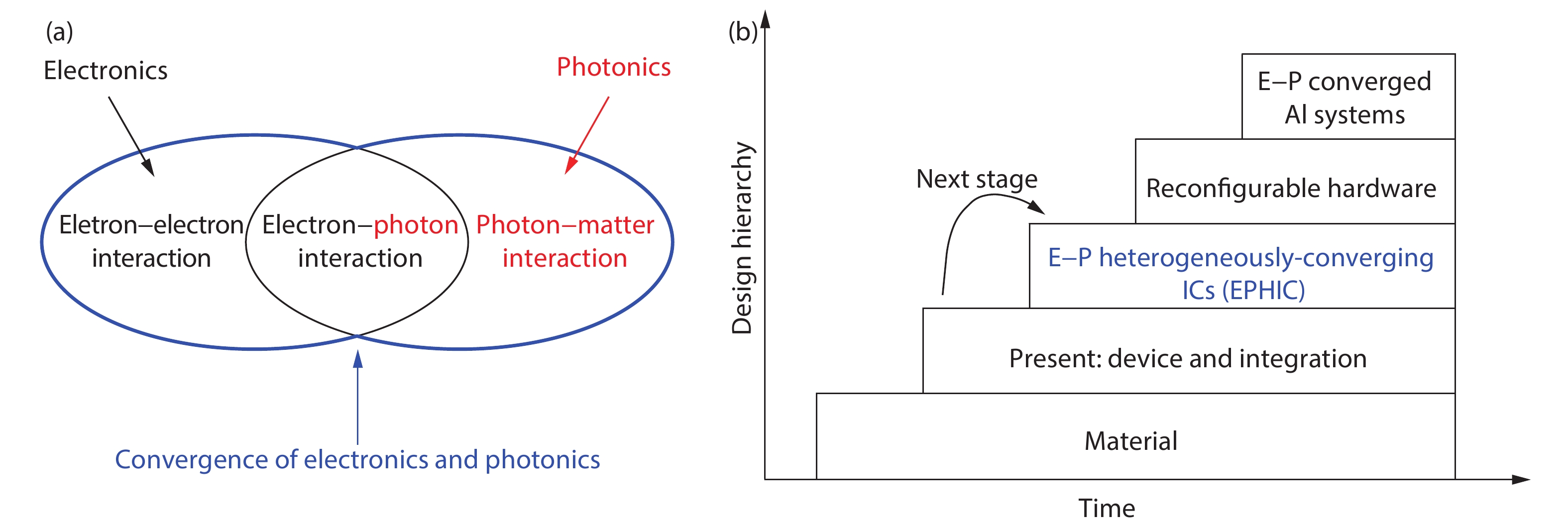
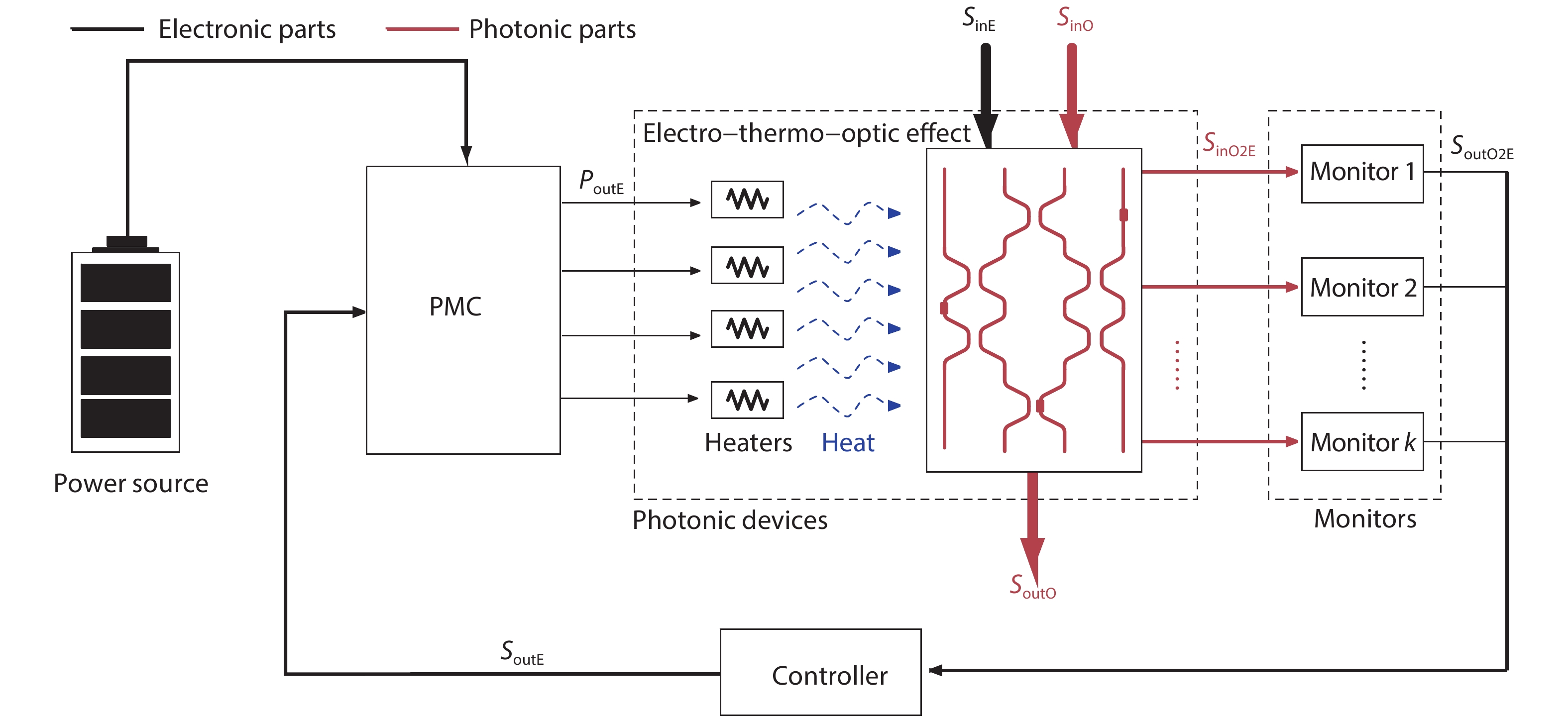
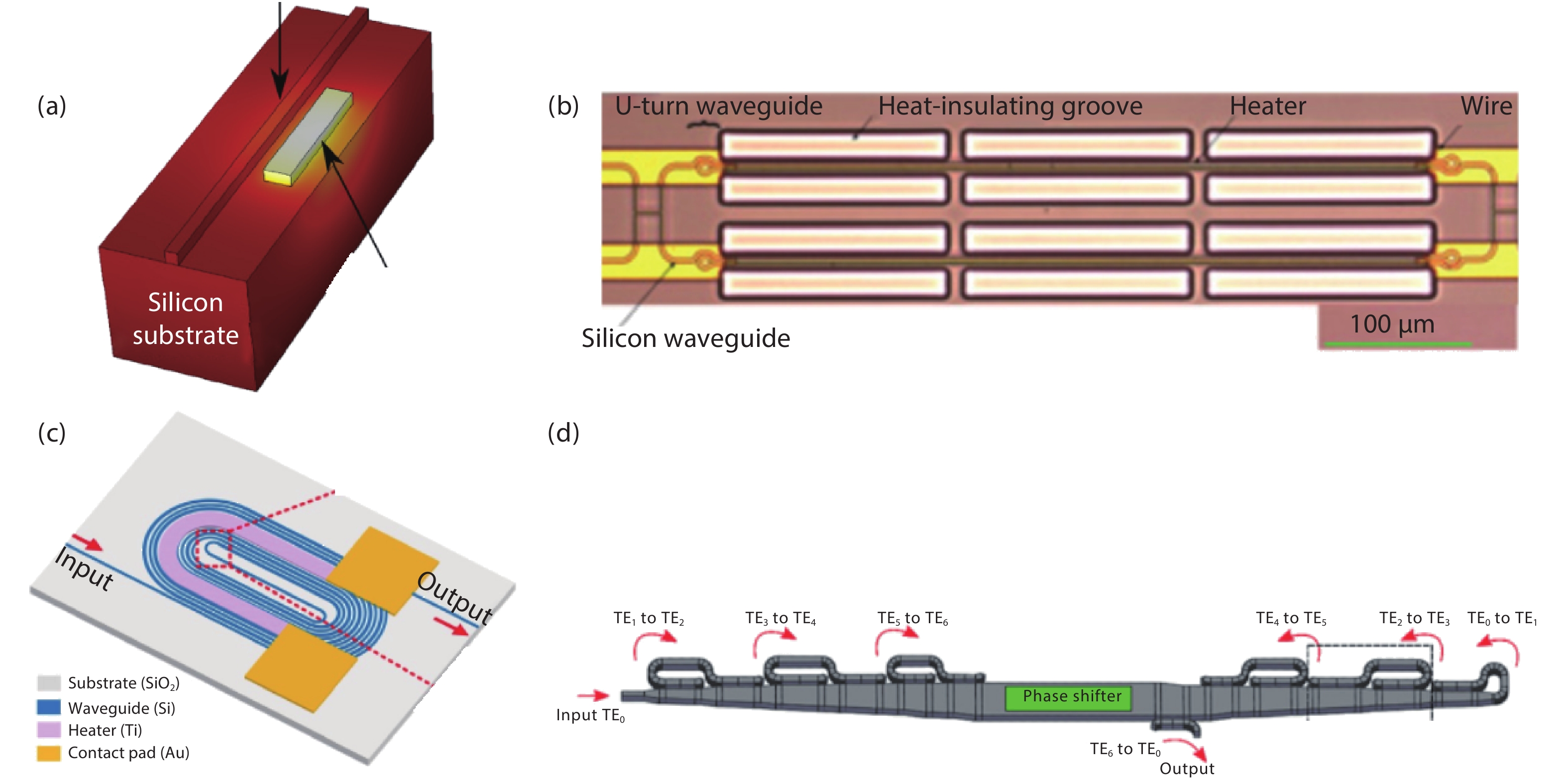
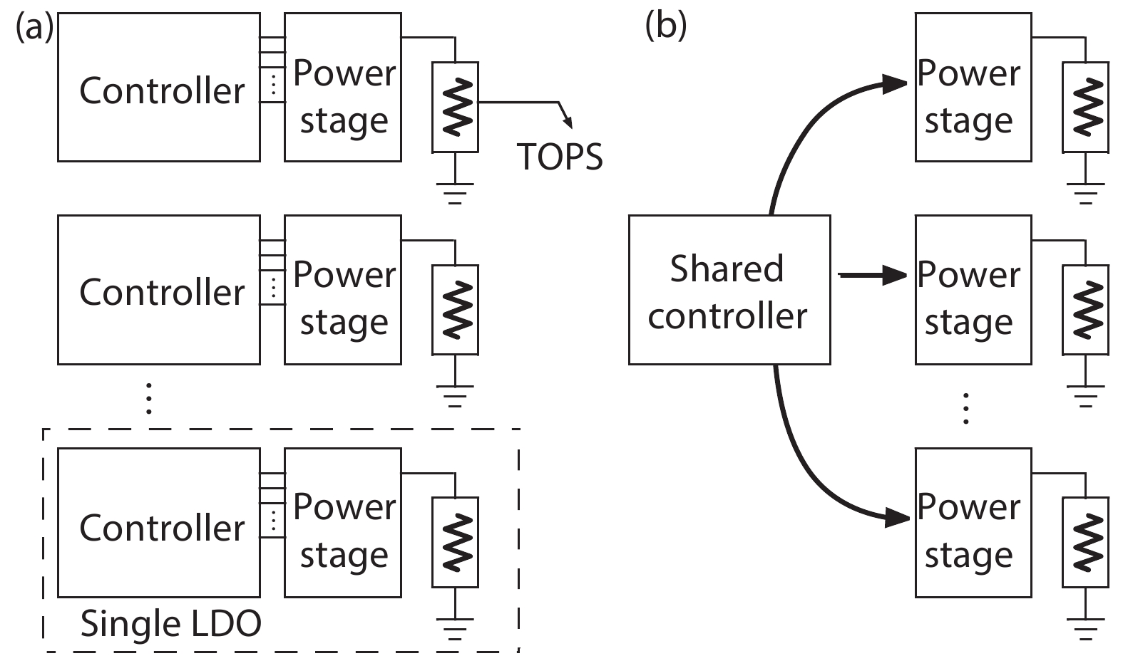
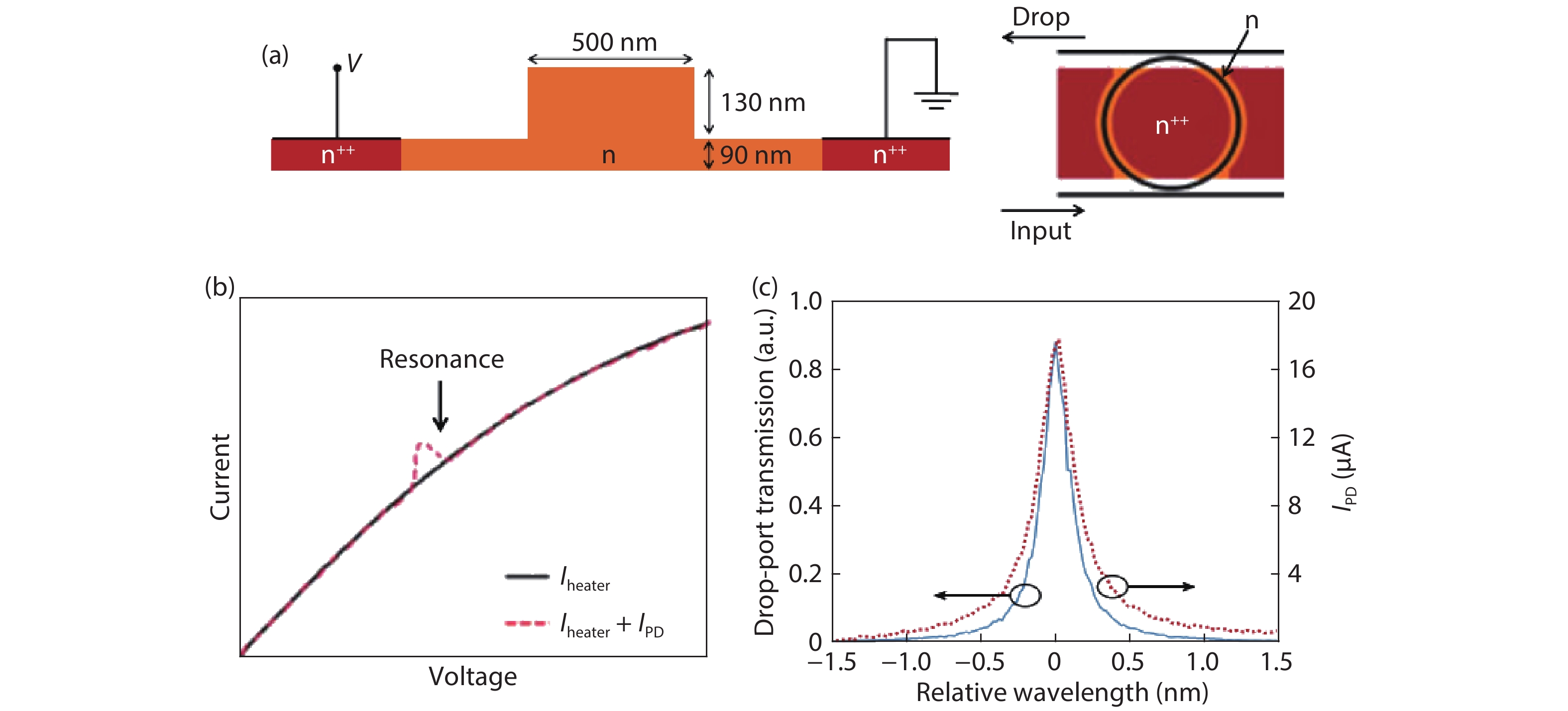
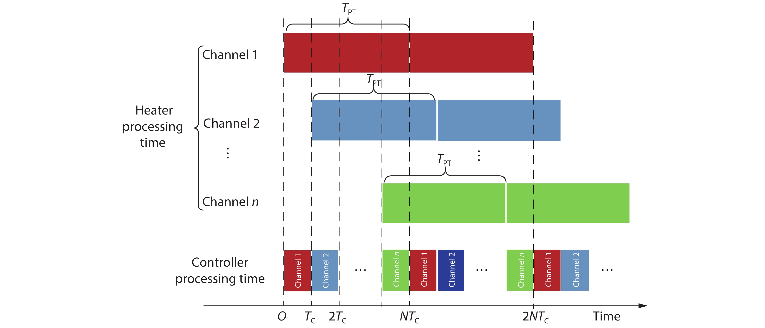
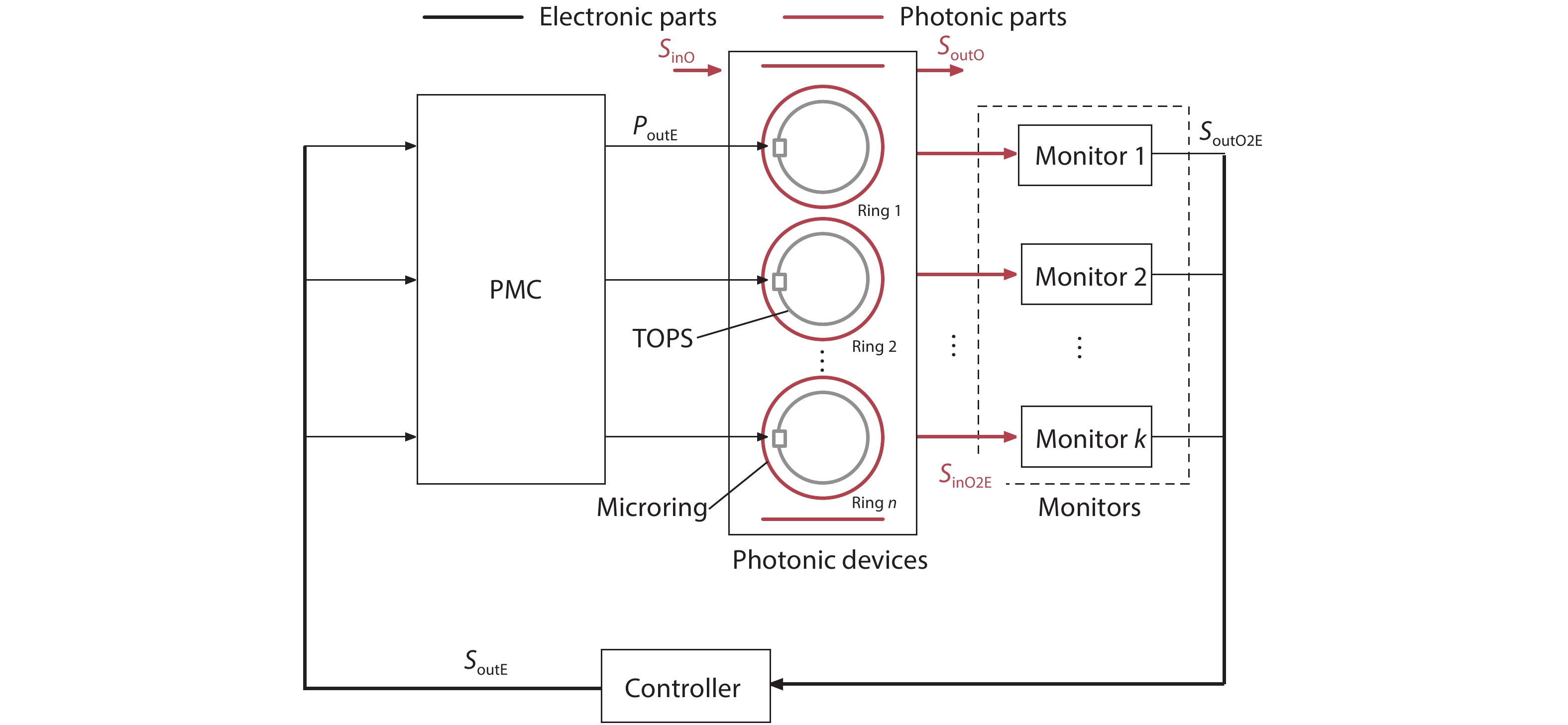
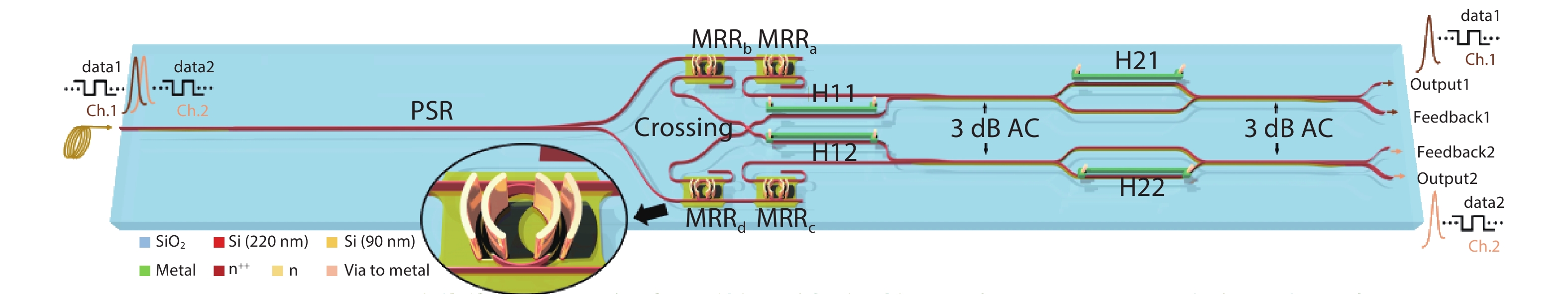
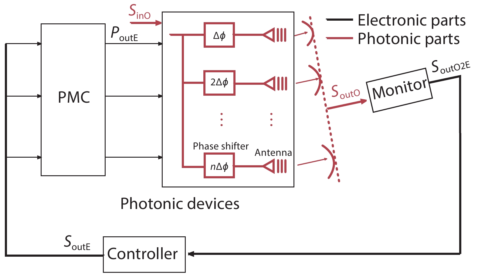
As Moore’s law approaching its end, electronics is hitting its power, bandwidth, and capacity limits. Photonics is able to overcome the performance limits of electronics but lacks practical photonic register and flexible control. Combining electronics and photonics provides the best of both worlds and is widely regarded as an important post-Moore’s direction. For stability and dynamic operations considerations, feedback tuning of photonic devices is required. For silicon photonics, the thermo-optic effect is the most frequently used tuning mechanism due to the advantages of high efficiency and low loss. However, it brings new design requirements, creating new design challenges. Emerging applications, such as optical phased array, optical switches, and optical neural networks, employ a large number of photonic devices, making PCB tuning solutions no longer suitable. Electronic-photonic-converged solutions with compact footprints will play an important role in system scalability. In this paper, we present a unified model for thermo-optic feedback tuning that can be specialized to different applications, review its recent advances, and discuss its future trends.


J. Semicond.
2021, 42(2): 023105 doi: 10.1088/1674-4926/42/2/023105
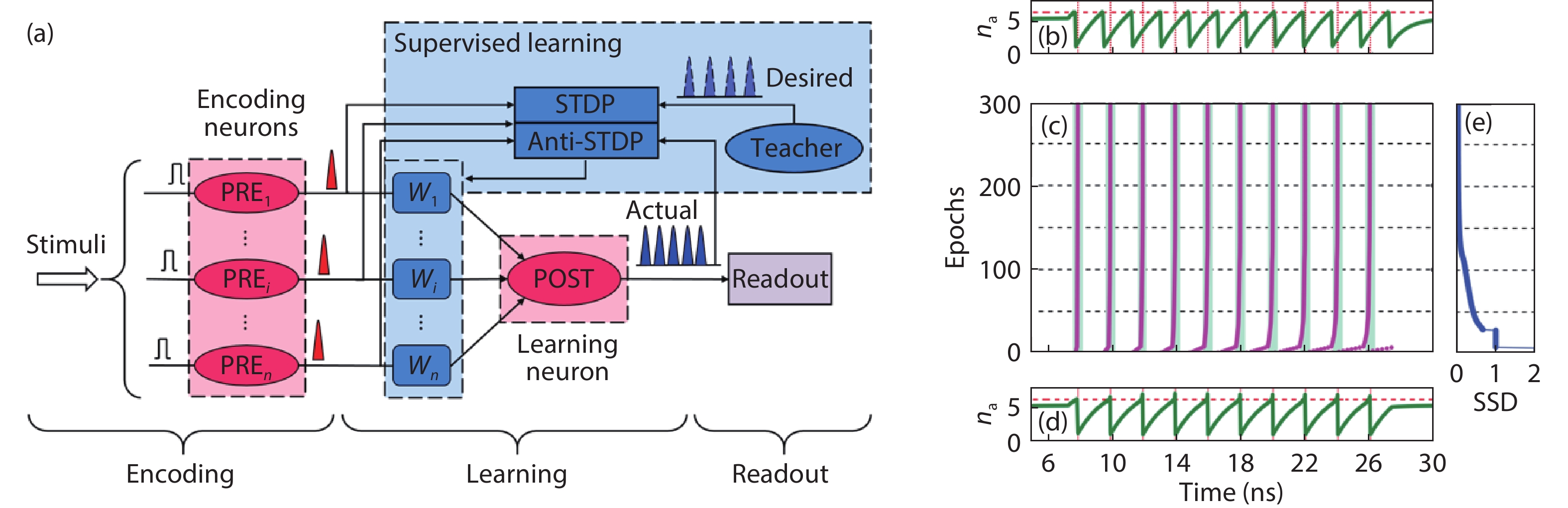
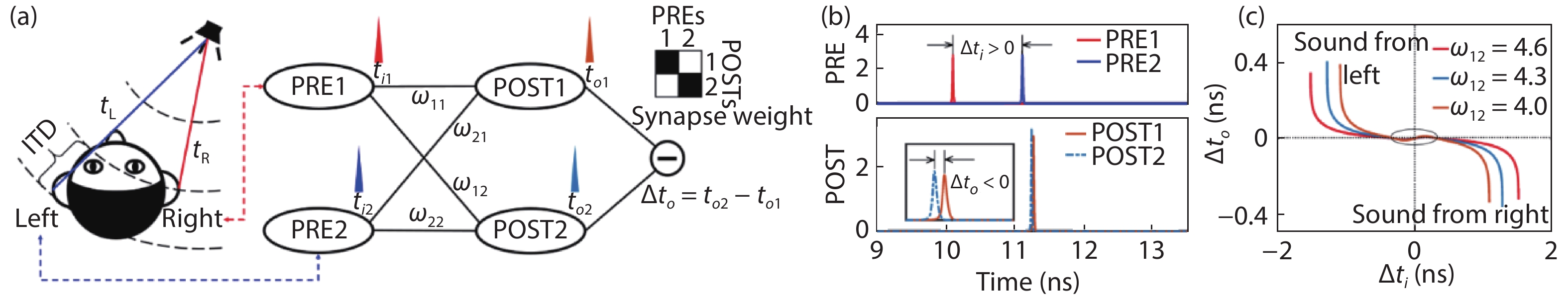
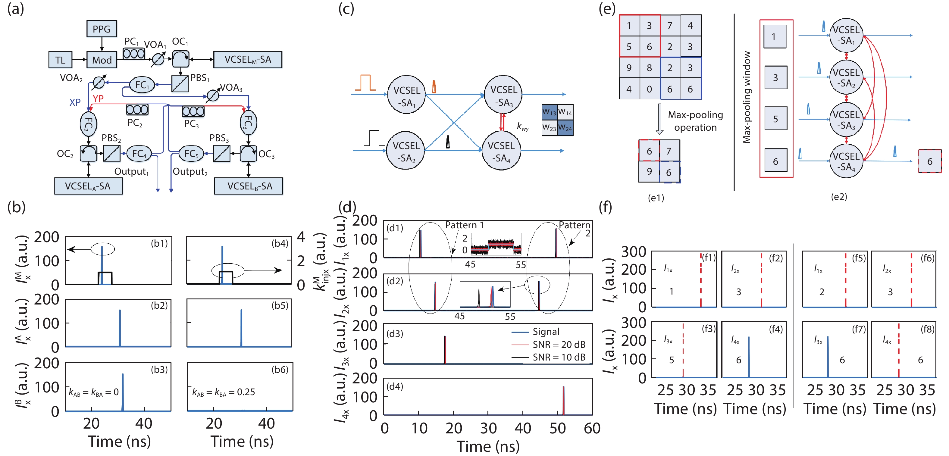
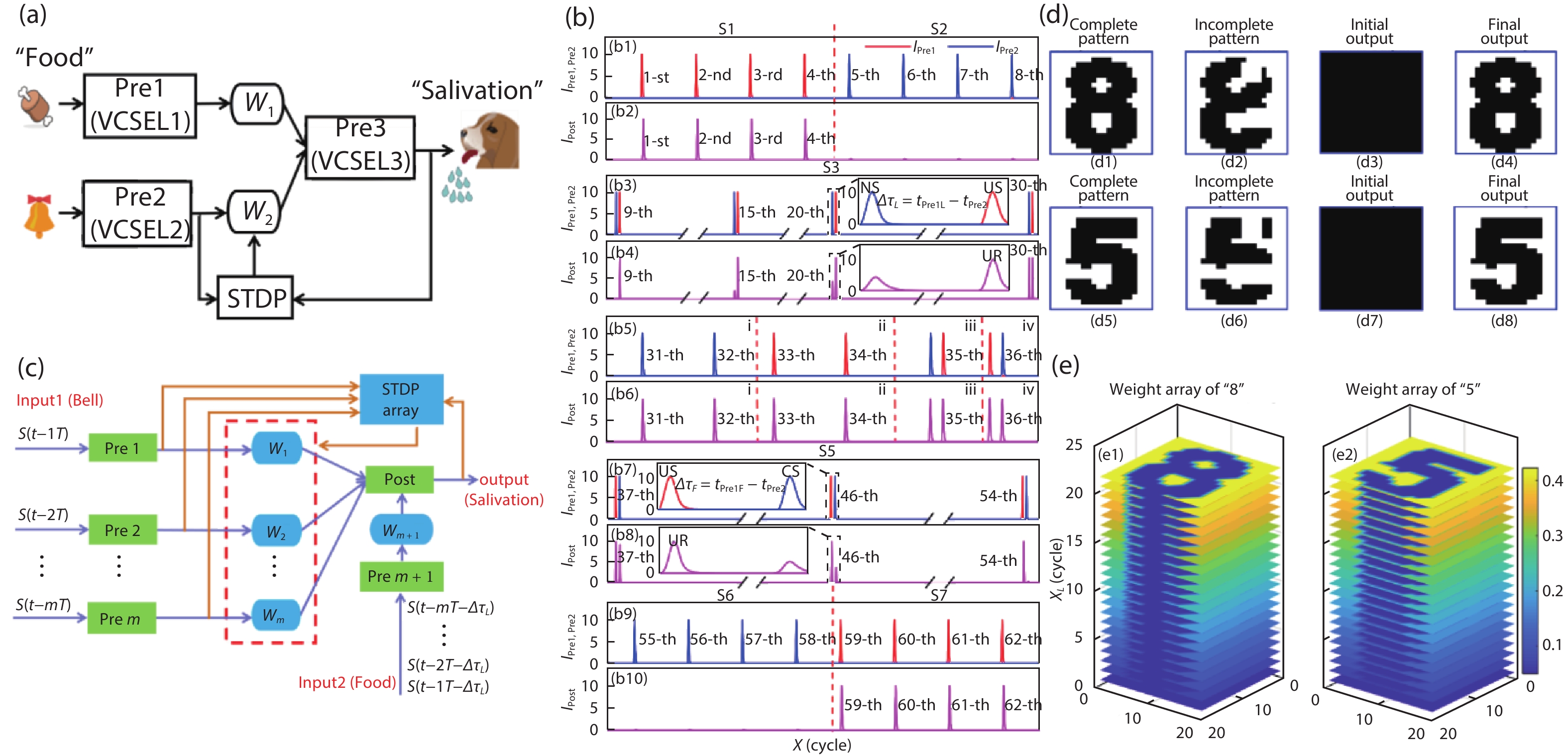
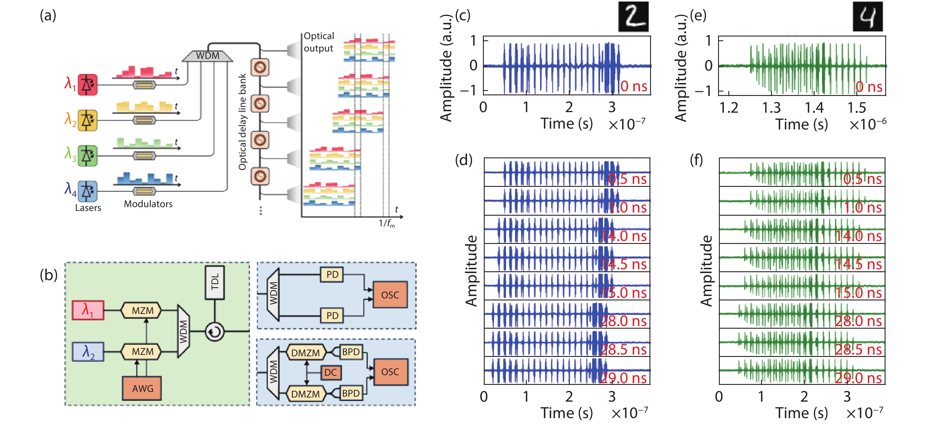
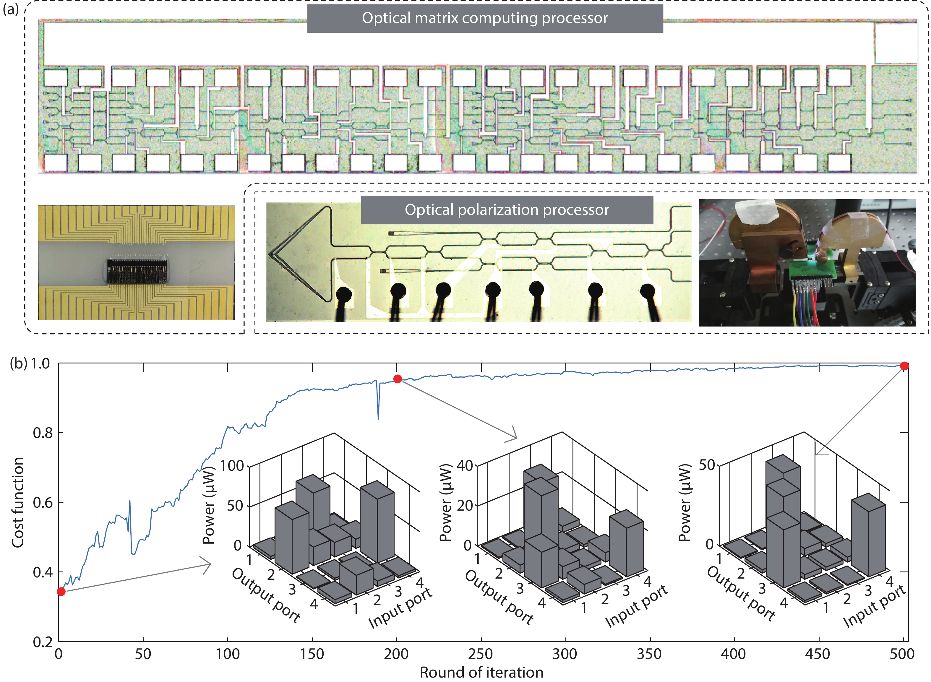
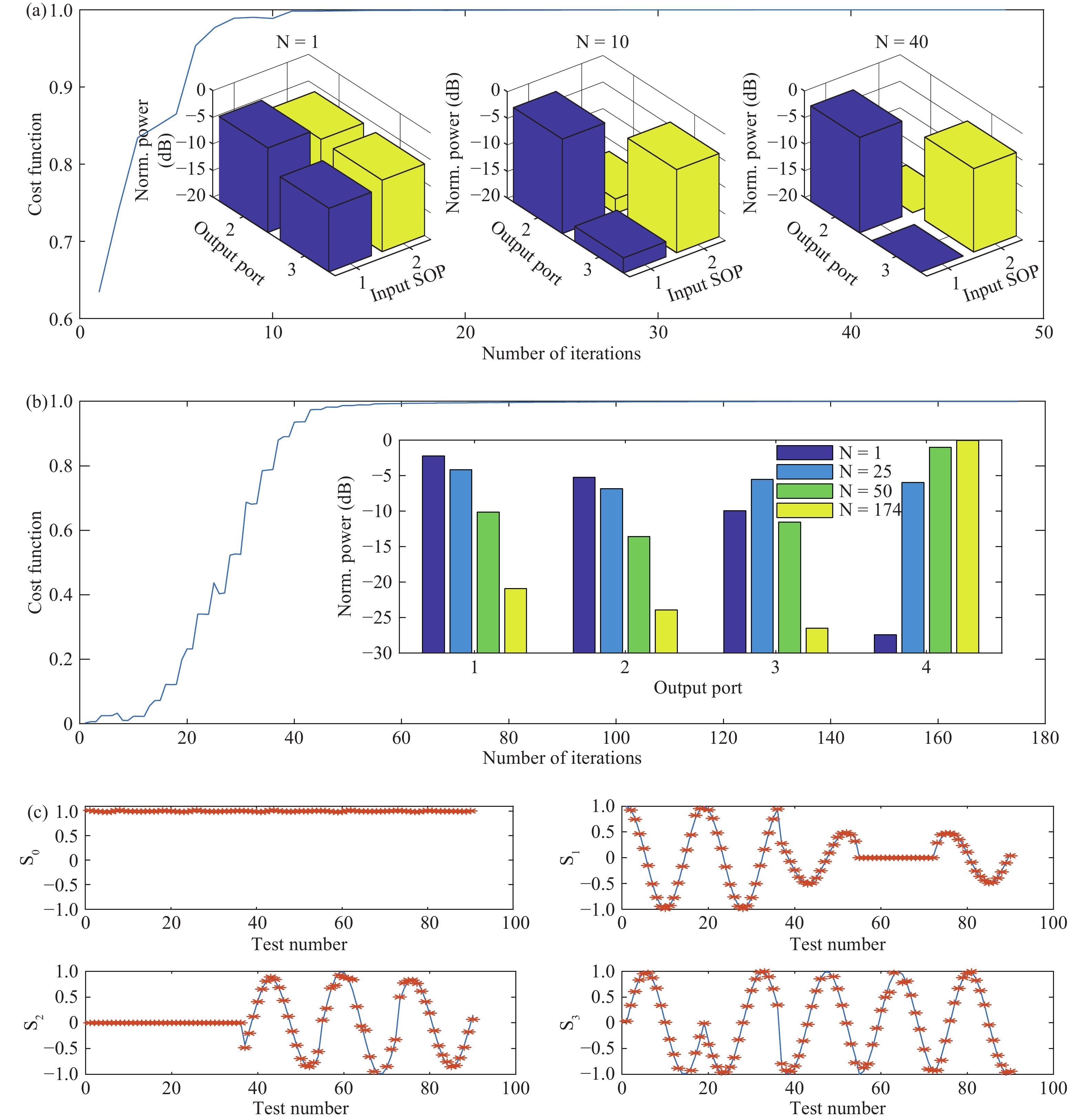
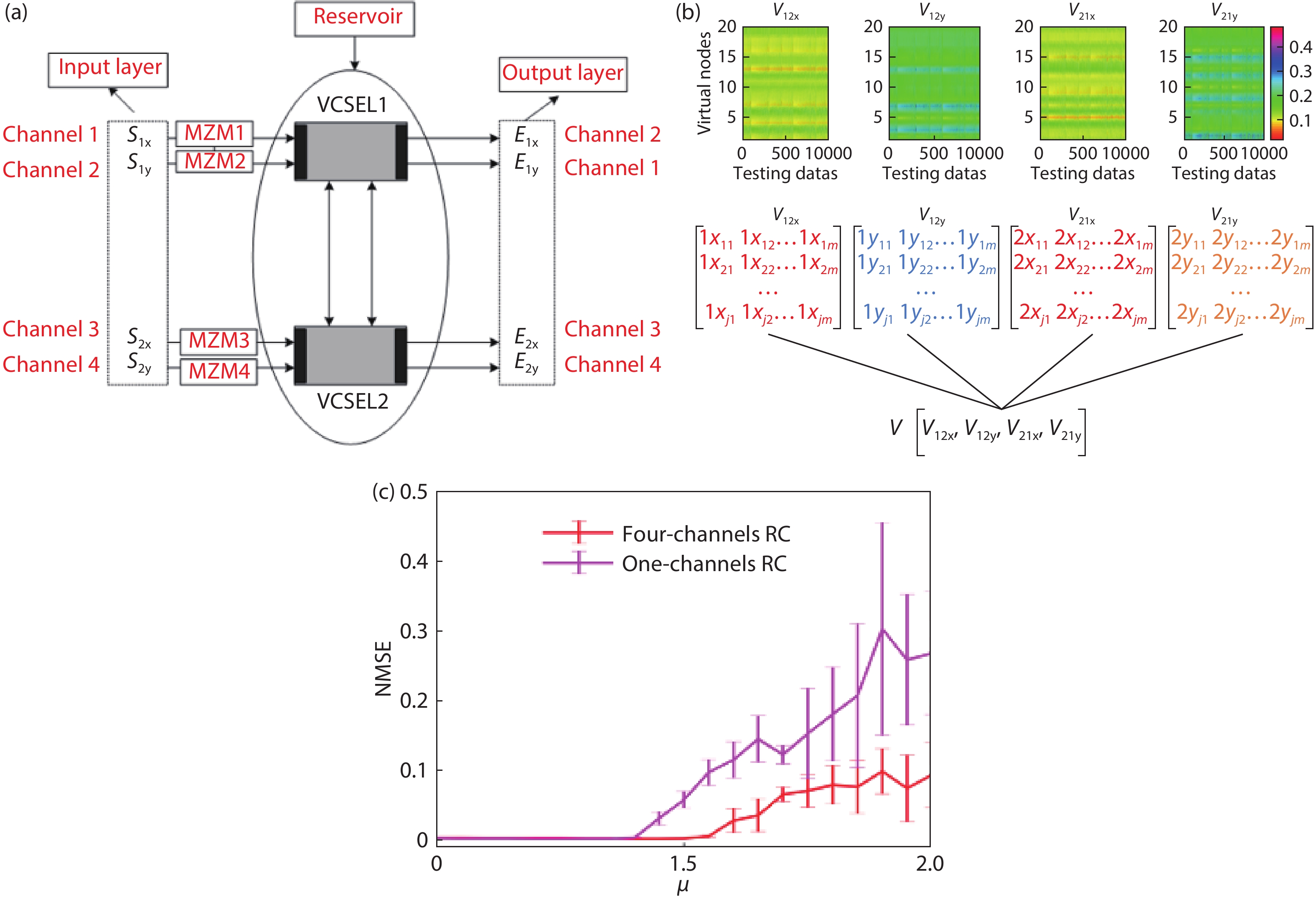
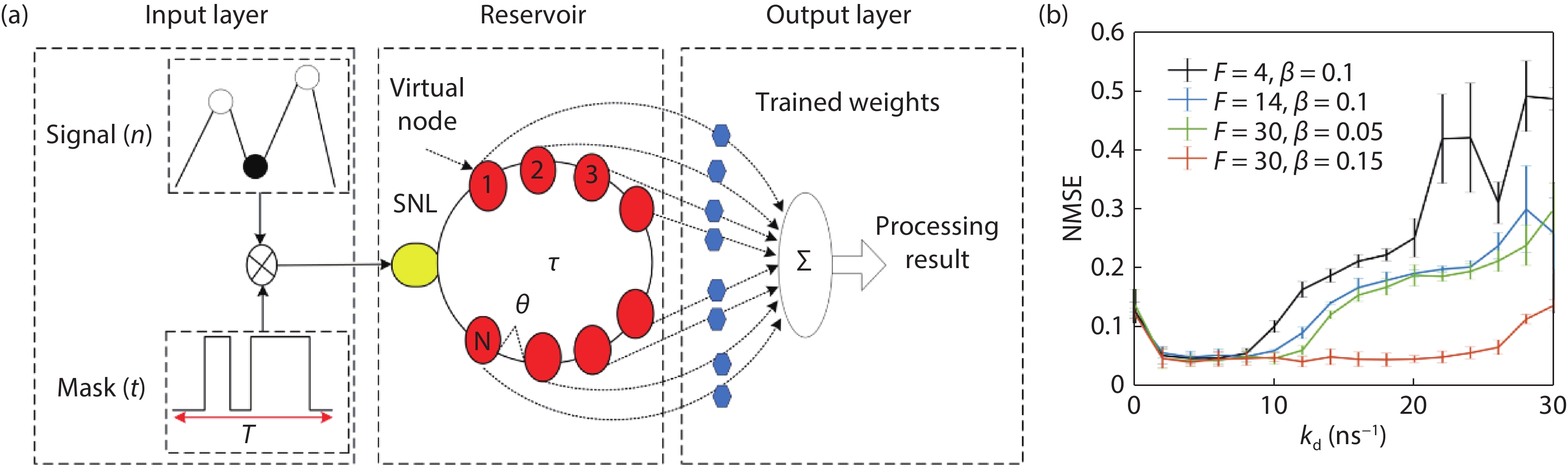
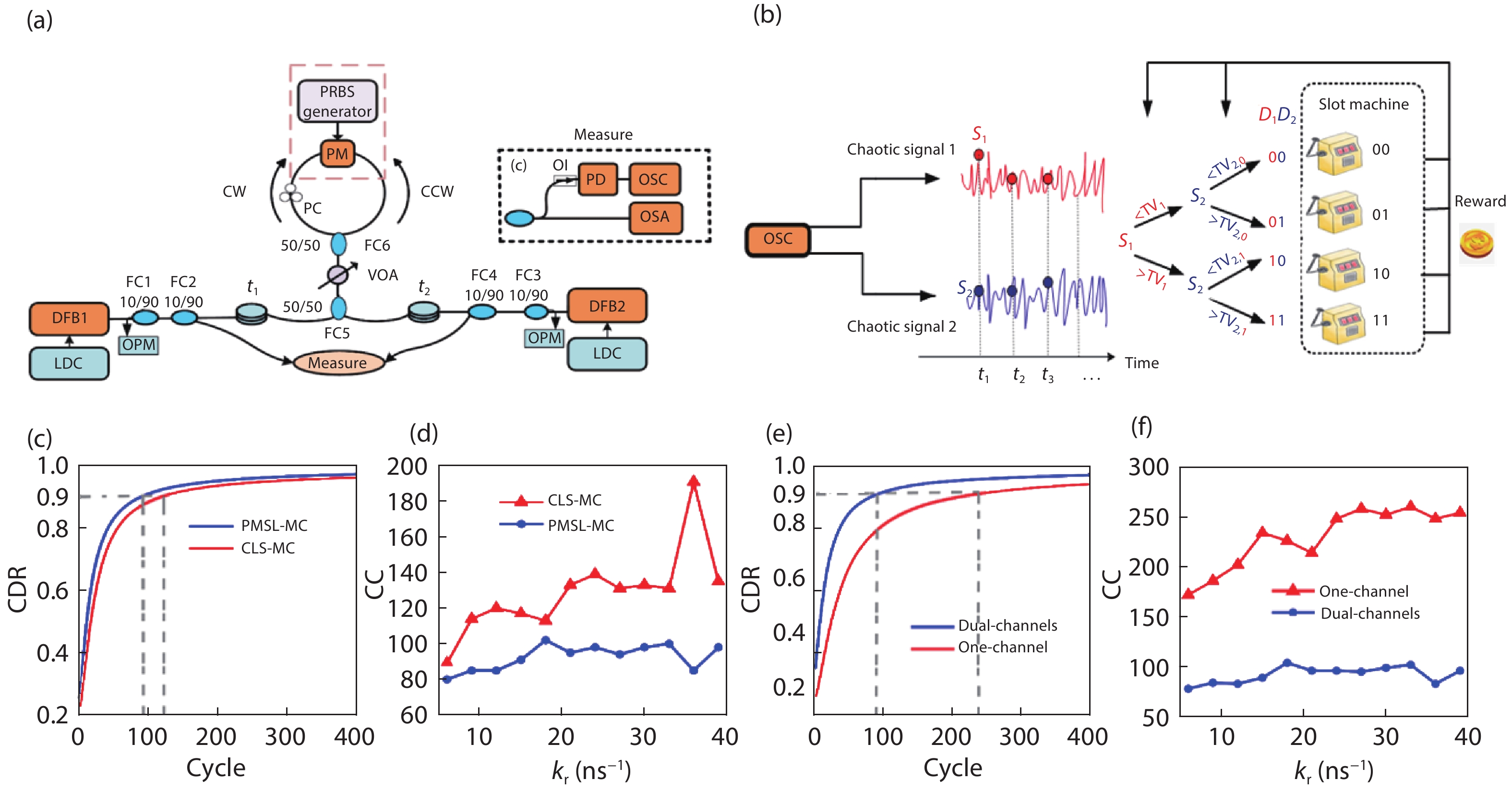
The explosive growth of data and information has motivated various emerging non-von Neumann computational approaches in the More-than-Moore era. Photonics neuromorphic computing has attracted lots of attention due to the fascinating advantages such as high speed, wide bandwidth, and massive parallelism. Here, we offer a review on the optical neural computing in our research groups at the device and system levels. The photonics neuron and photonics synapse plasticity are presented. In addition, we introduce several optical neural computing architectures and algorithms including photonic spiking neural network, photonic convolutional neural network, photonic matrix computation, photonic reservoir computing, and photonic reinforcement learning. Finally, we summarize the major challenges faced by photonic neuromorphic computing, and propose promising solutions and perspectives.


J. Semicond.
2021, 42(2): 023106 doi: 10.1088/1674-4926/42/2/023106
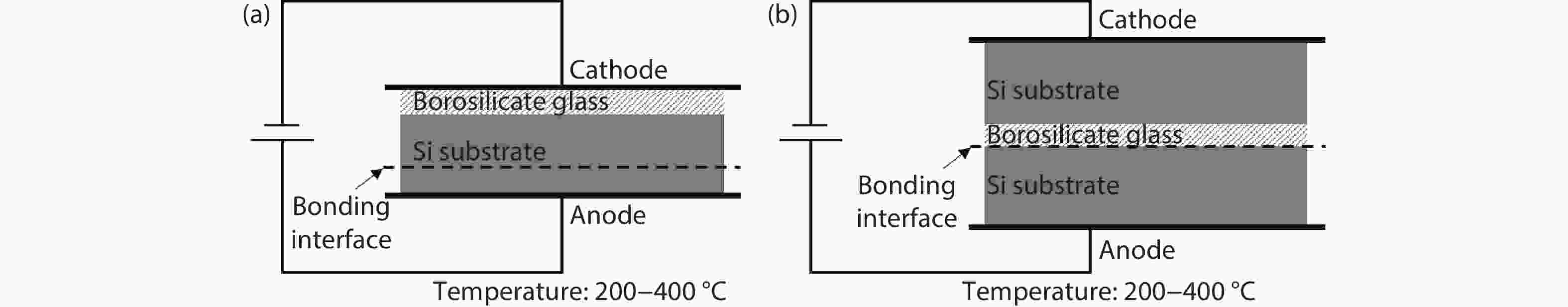
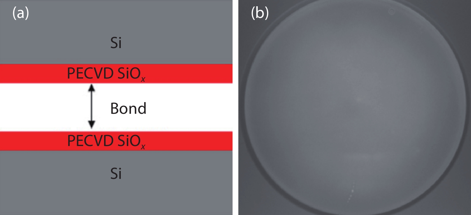
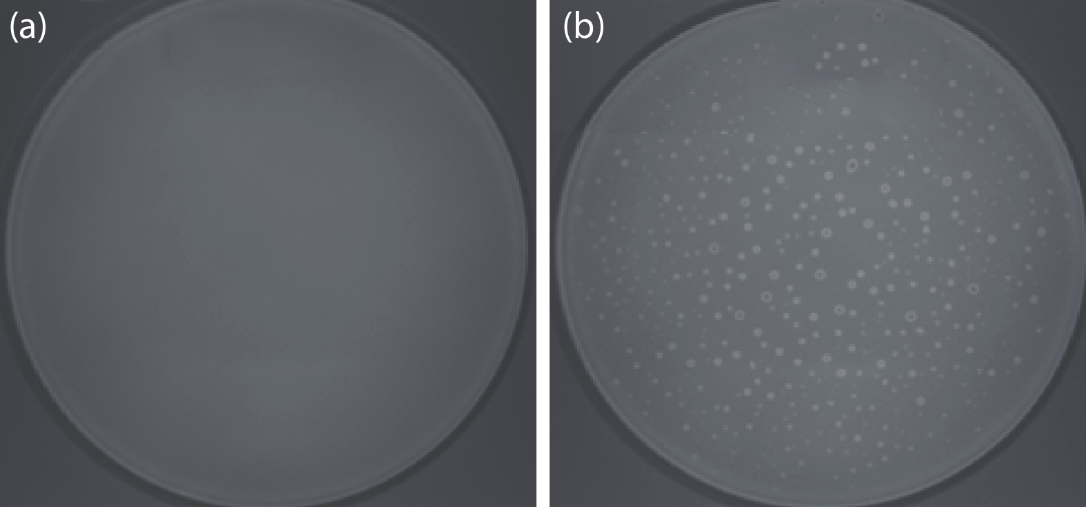
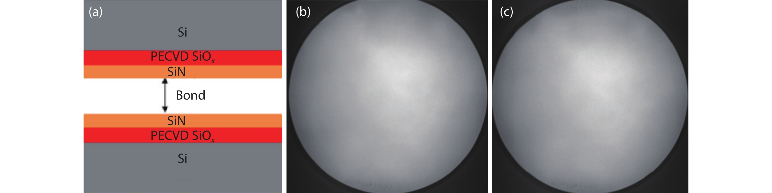
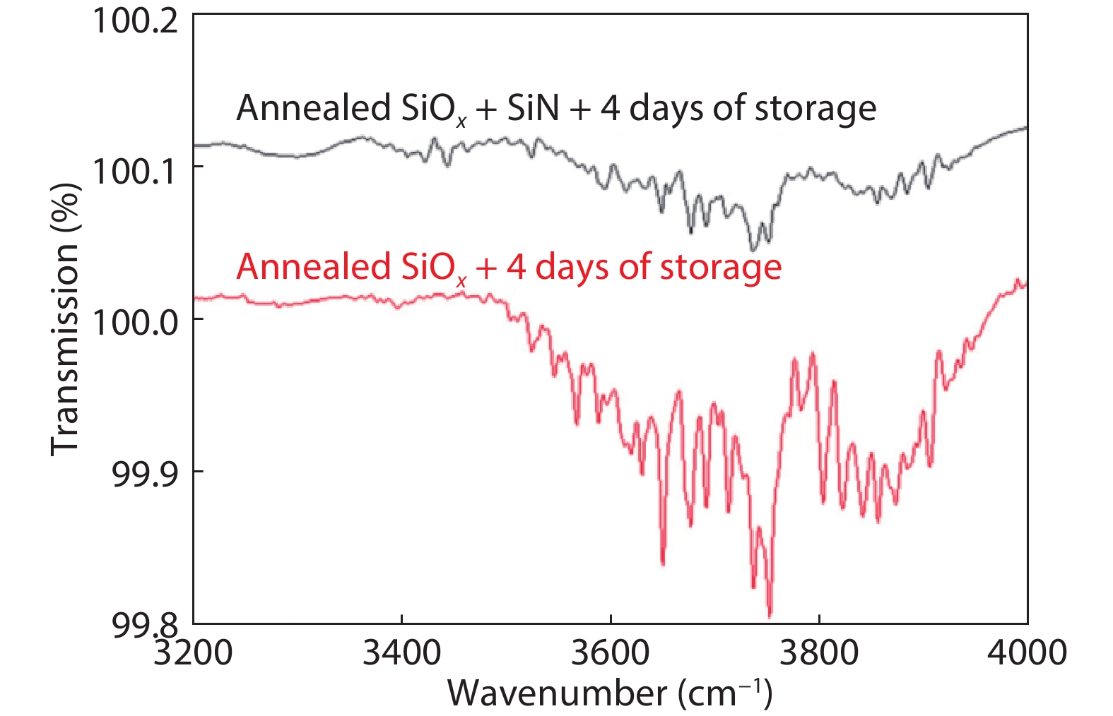
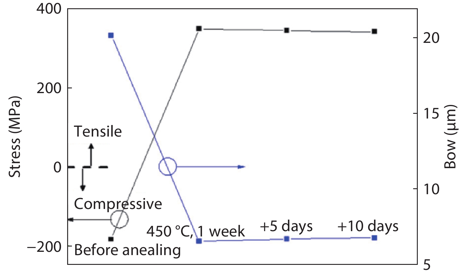
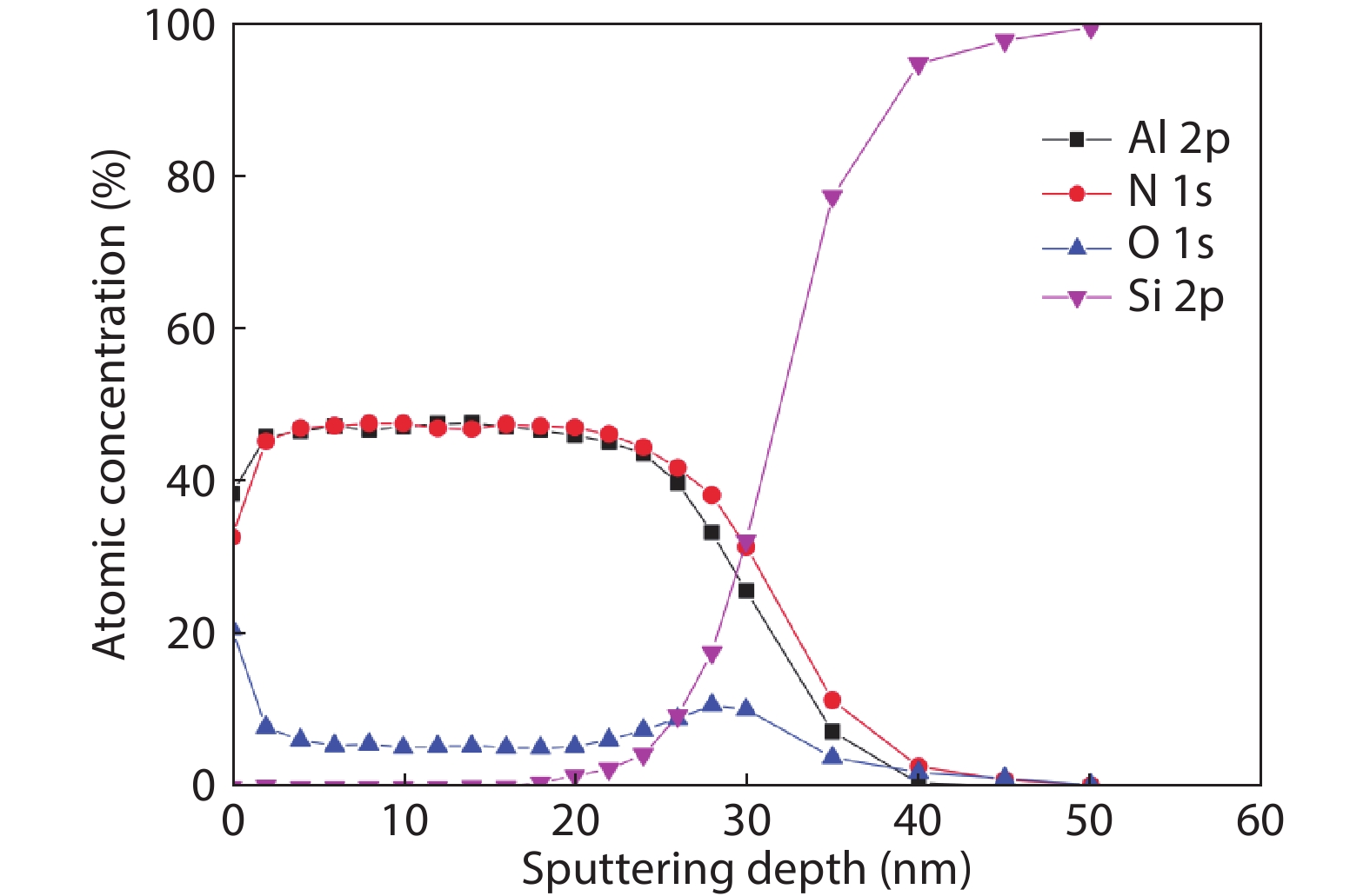
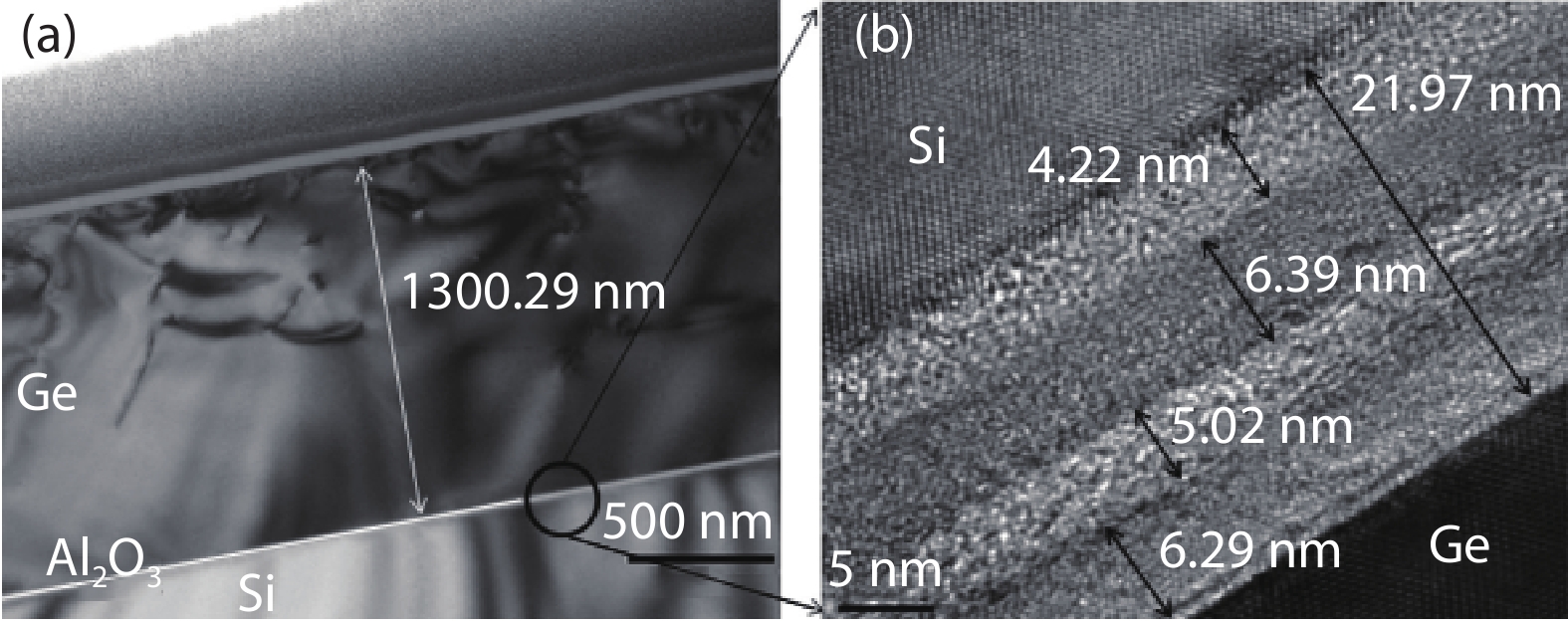
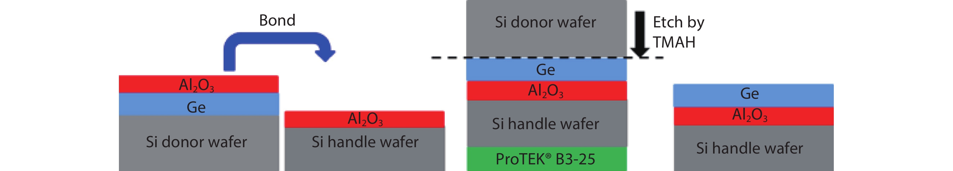
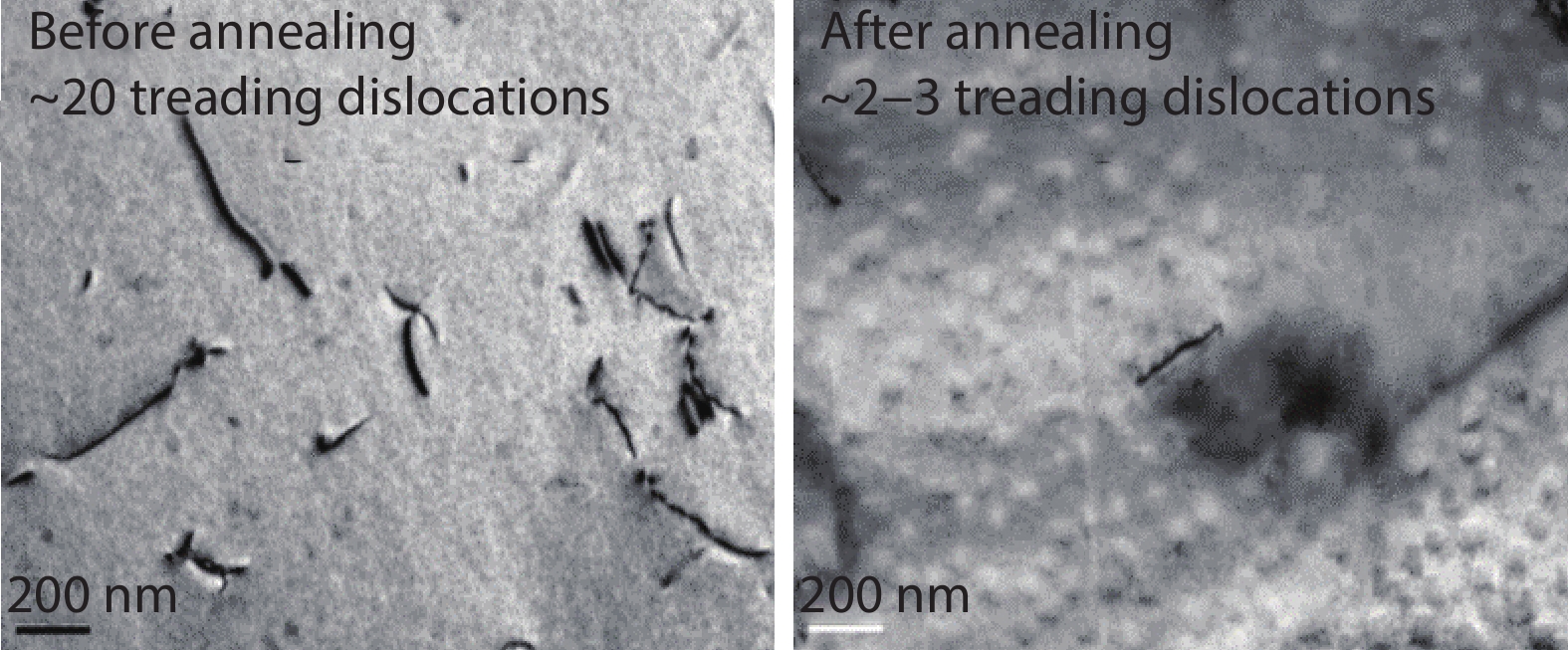
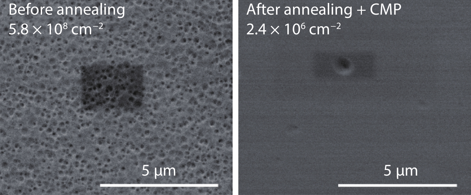
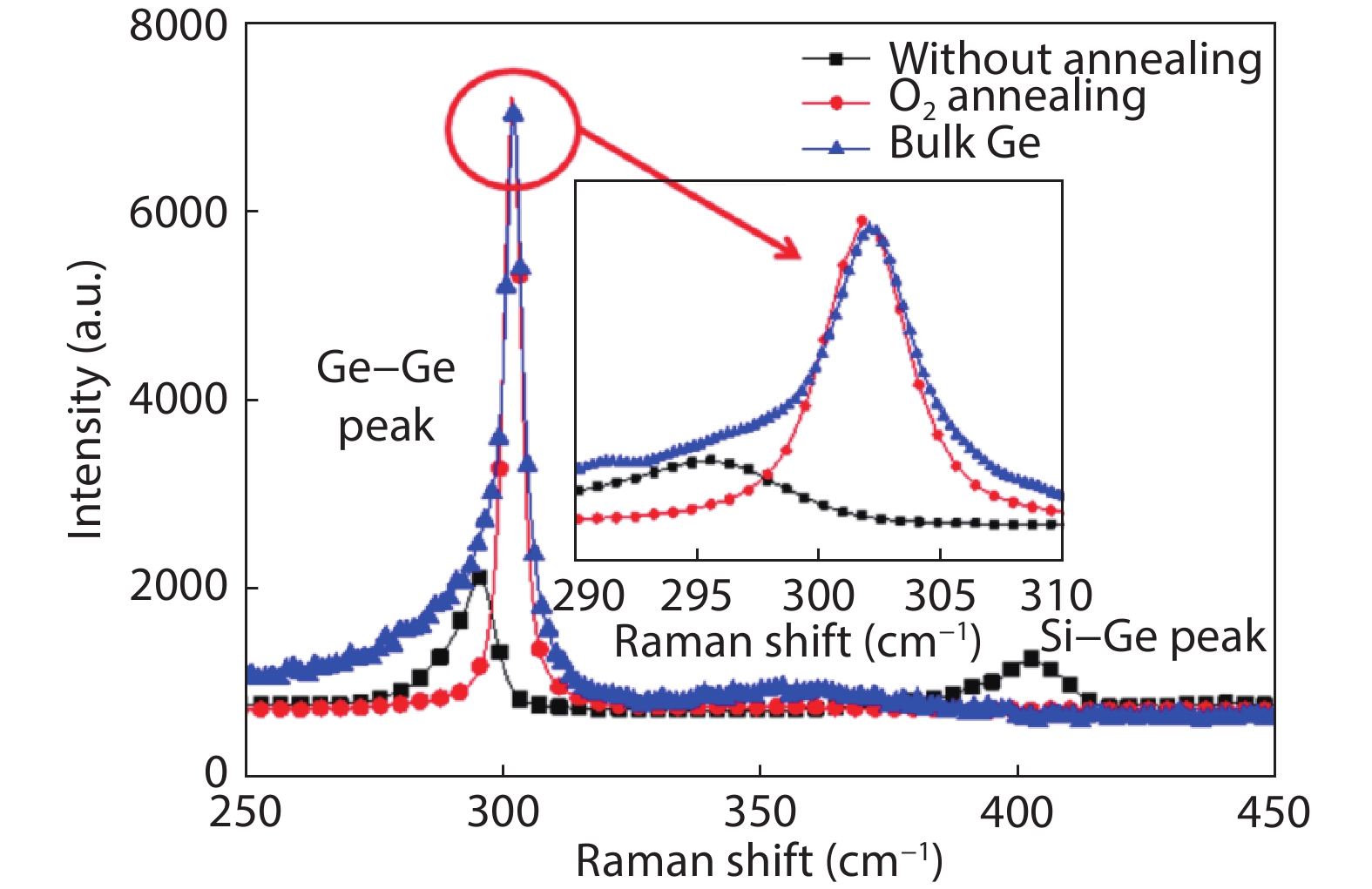
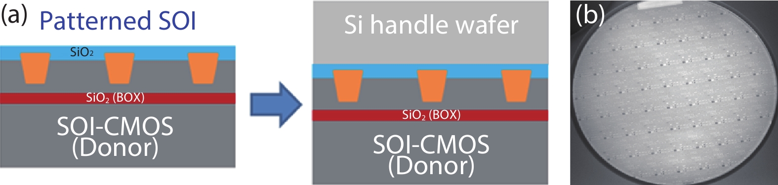
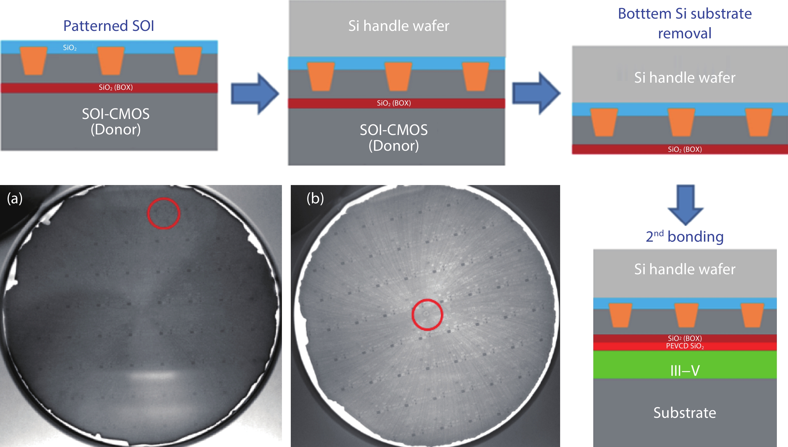
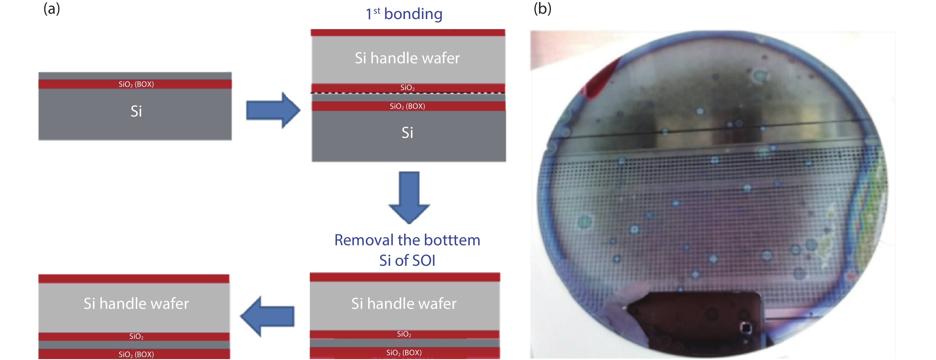
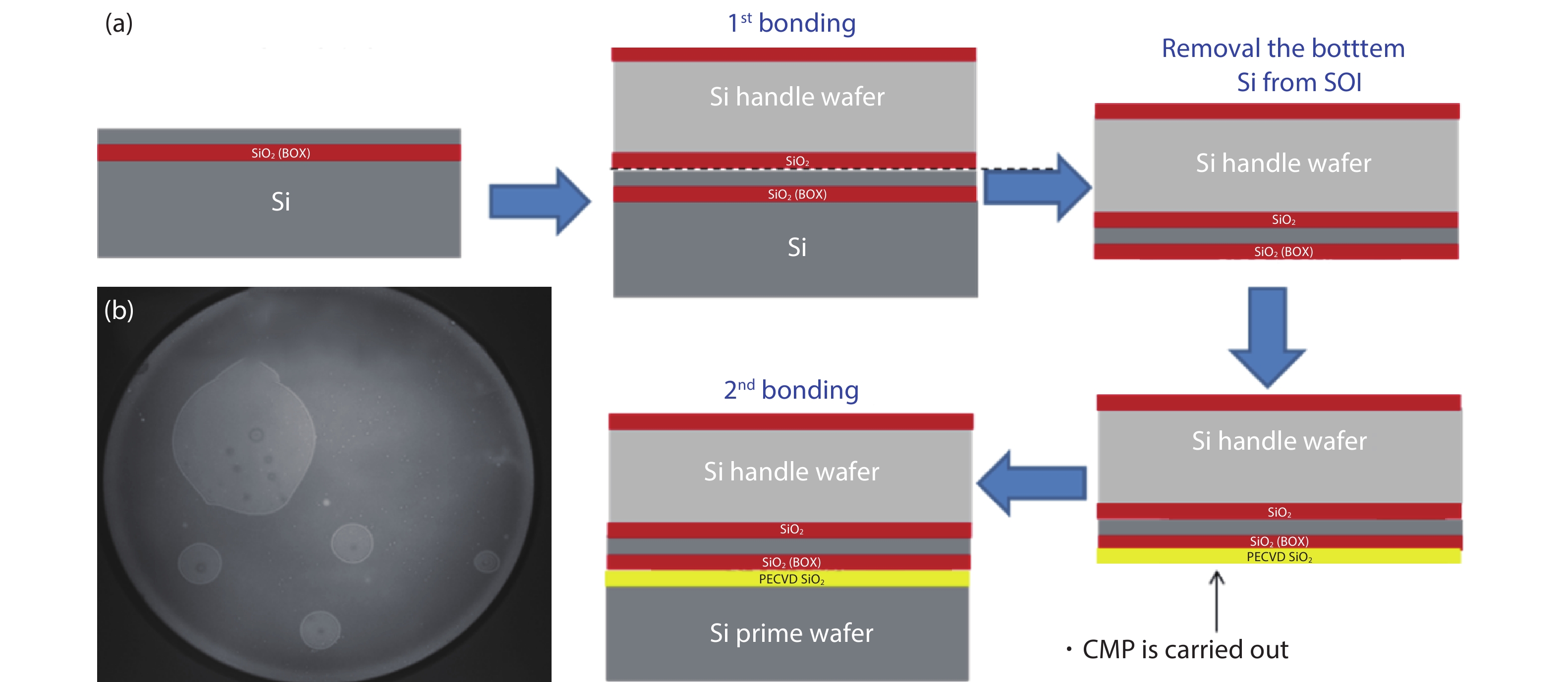
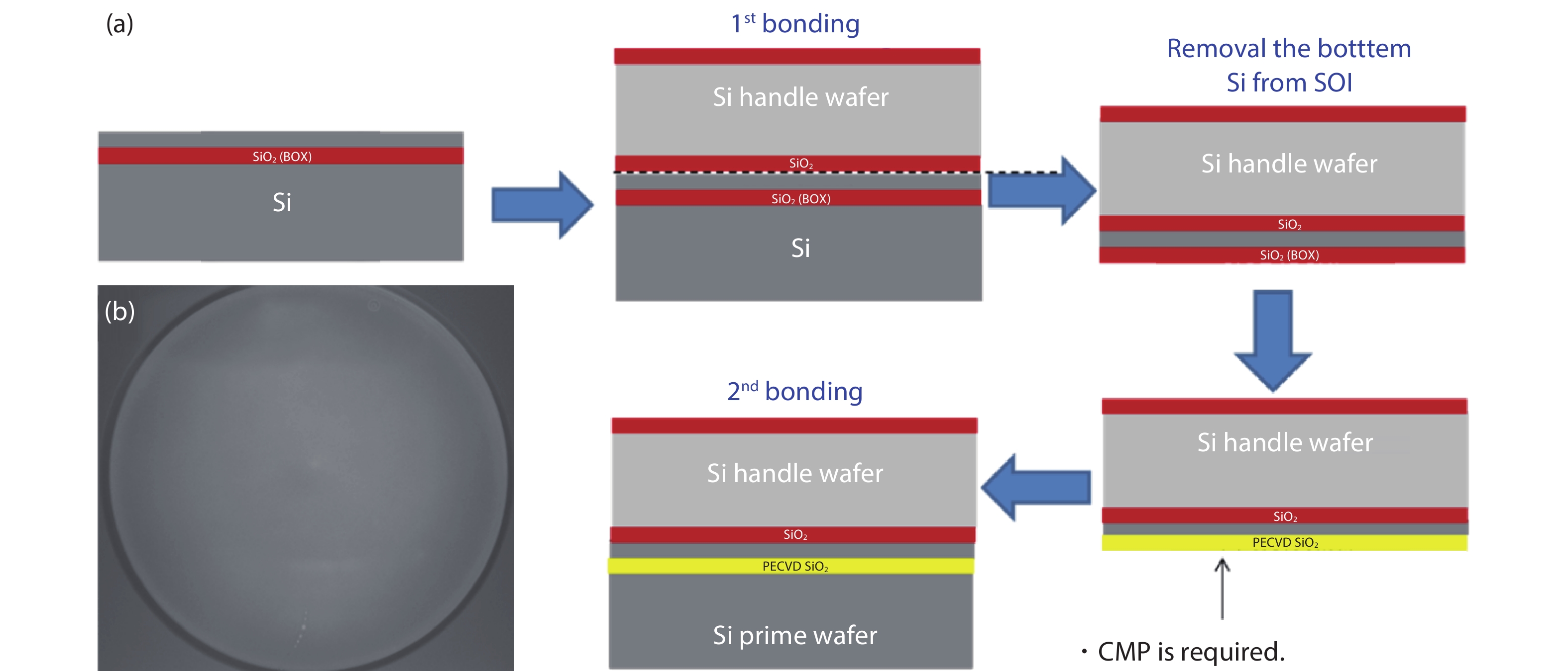
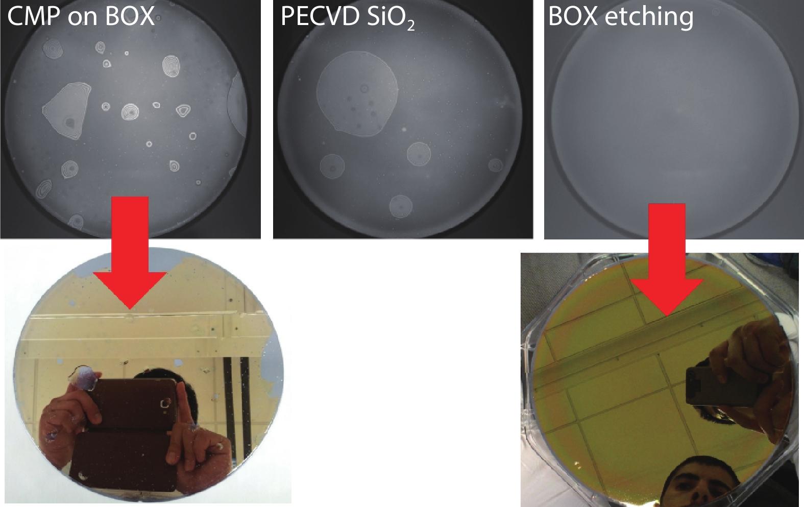
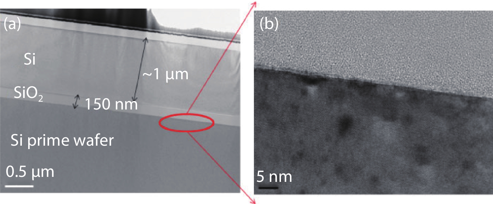
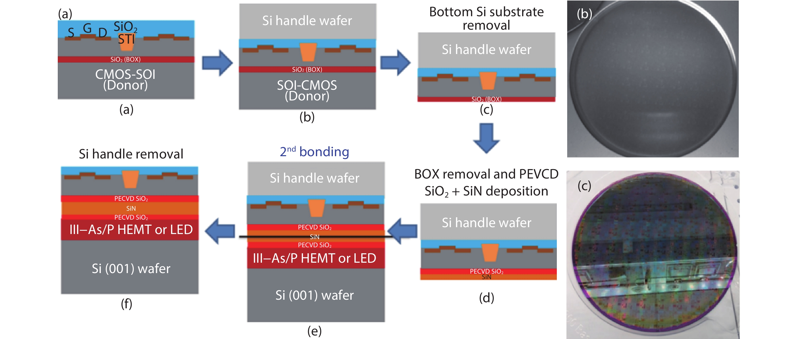
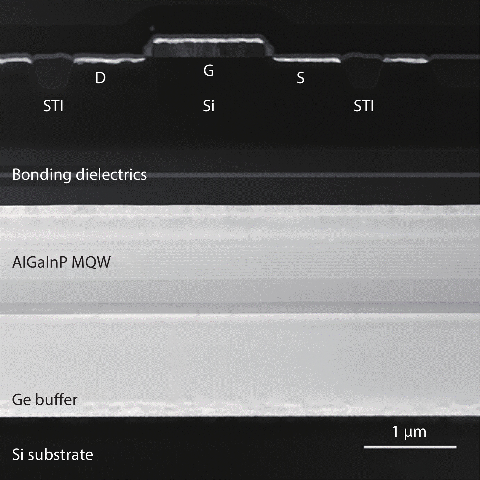
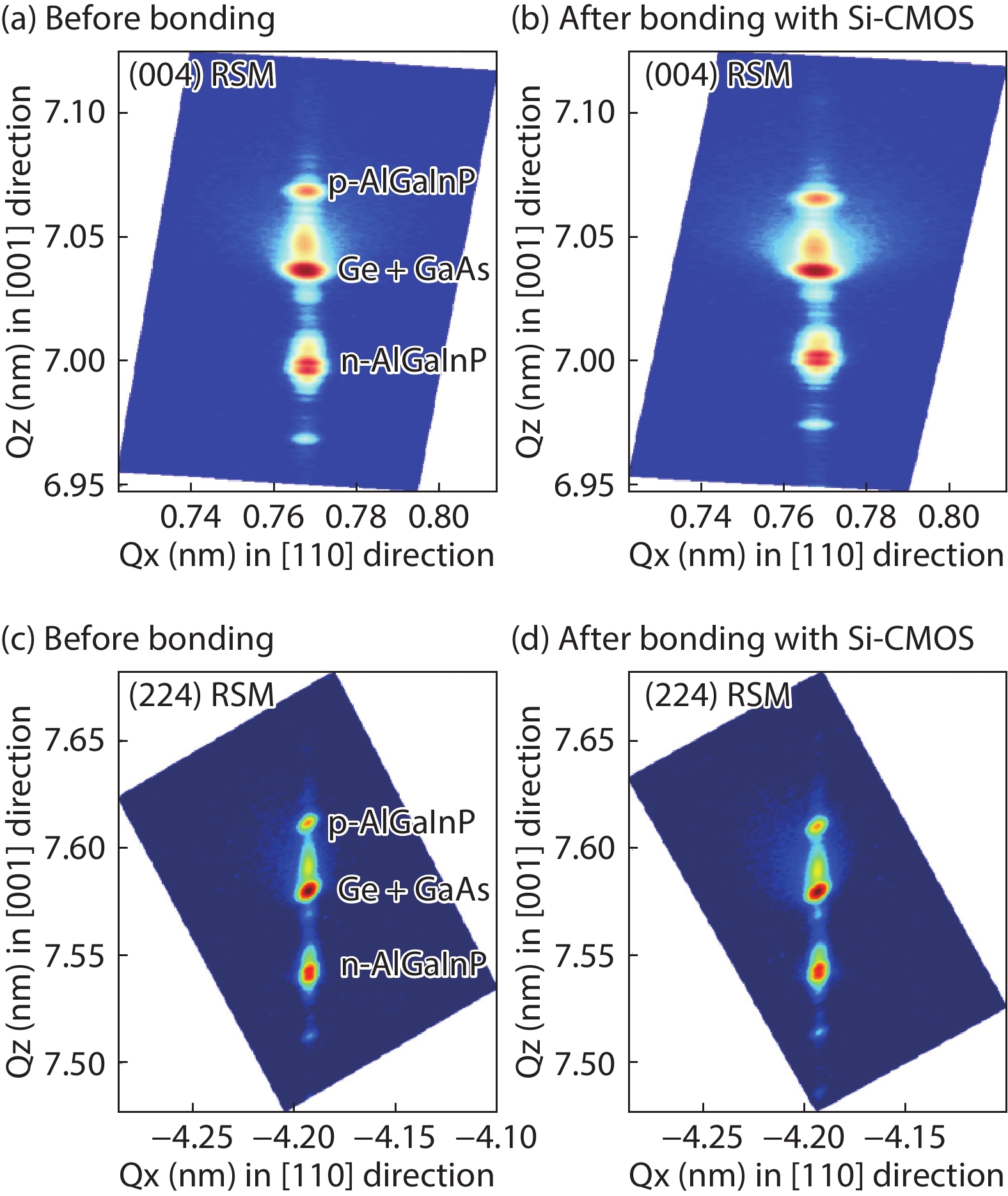
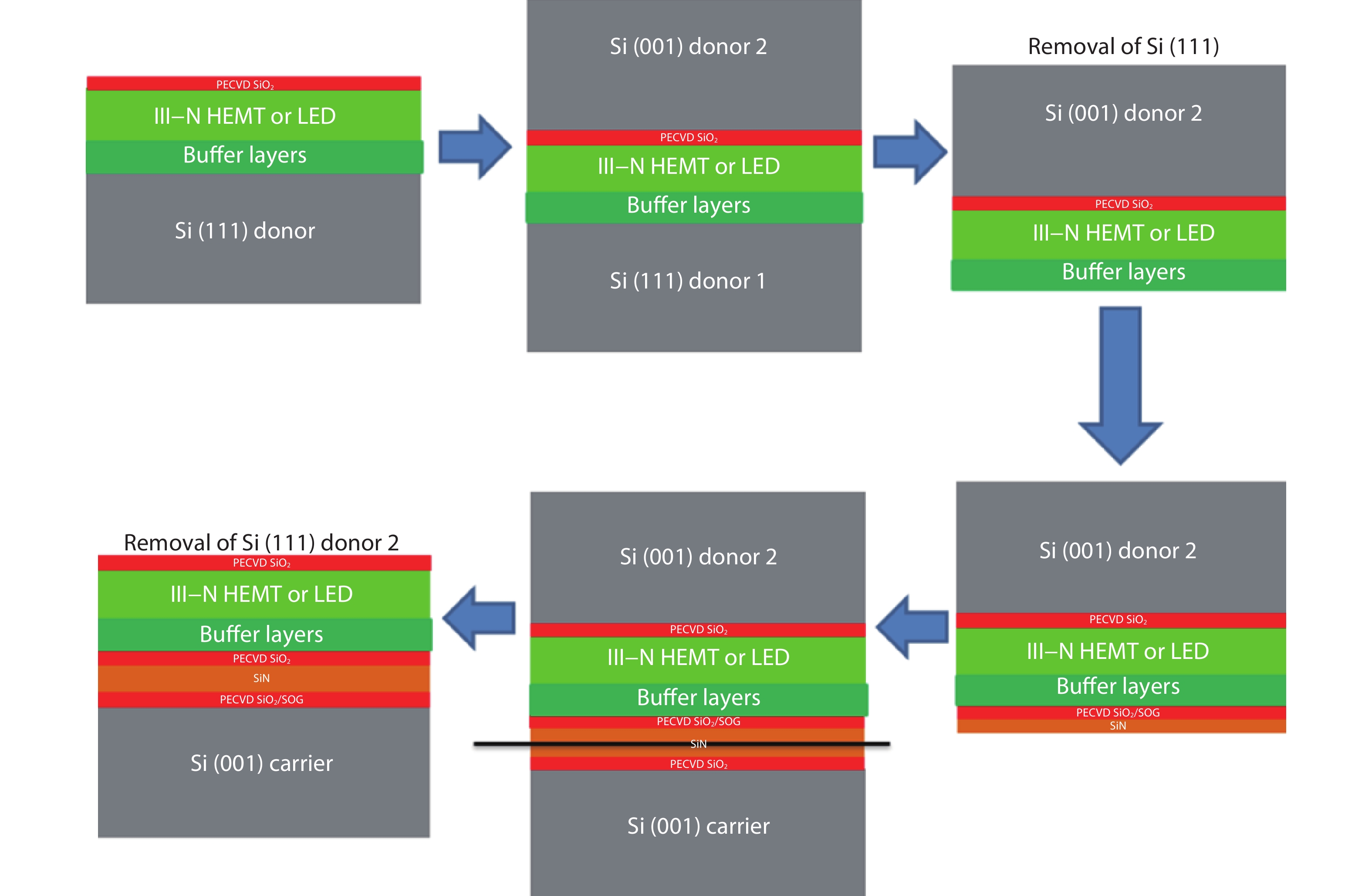
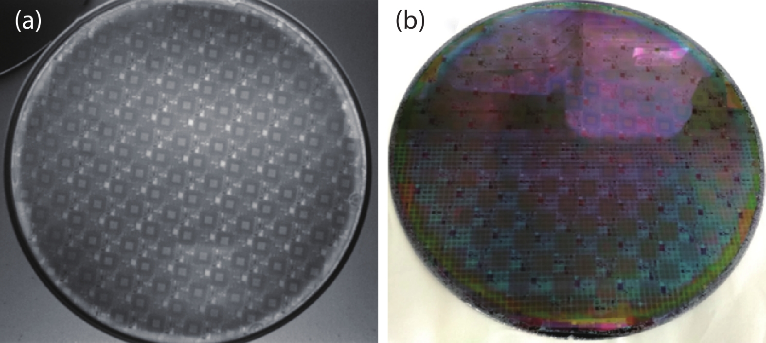
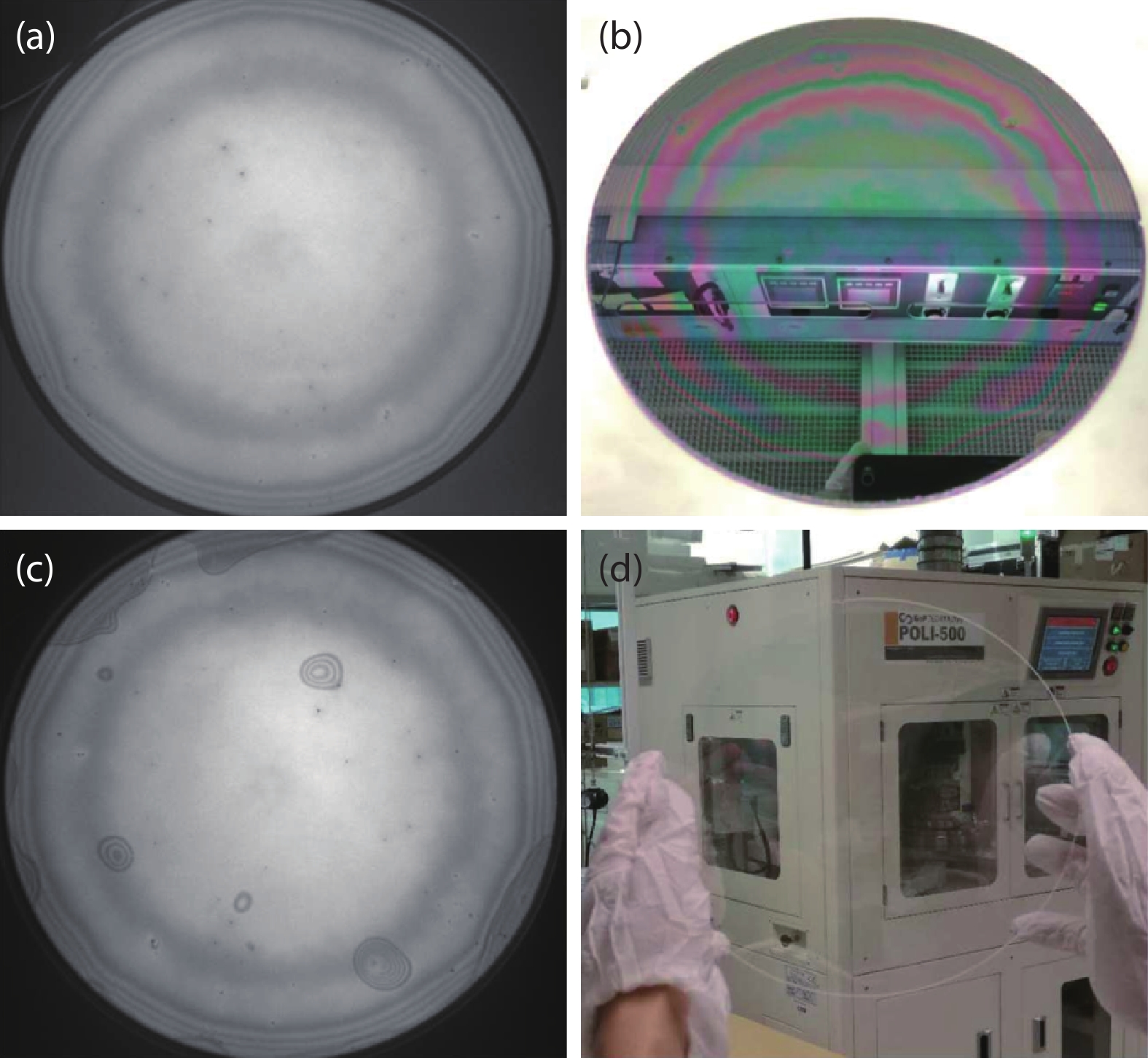
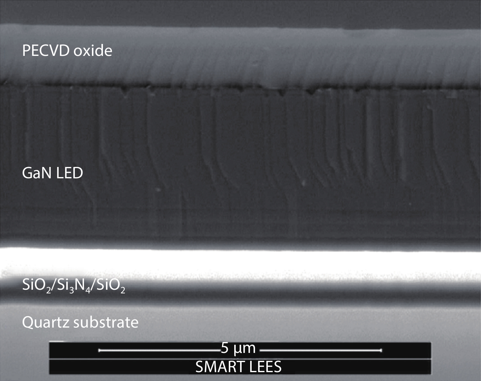
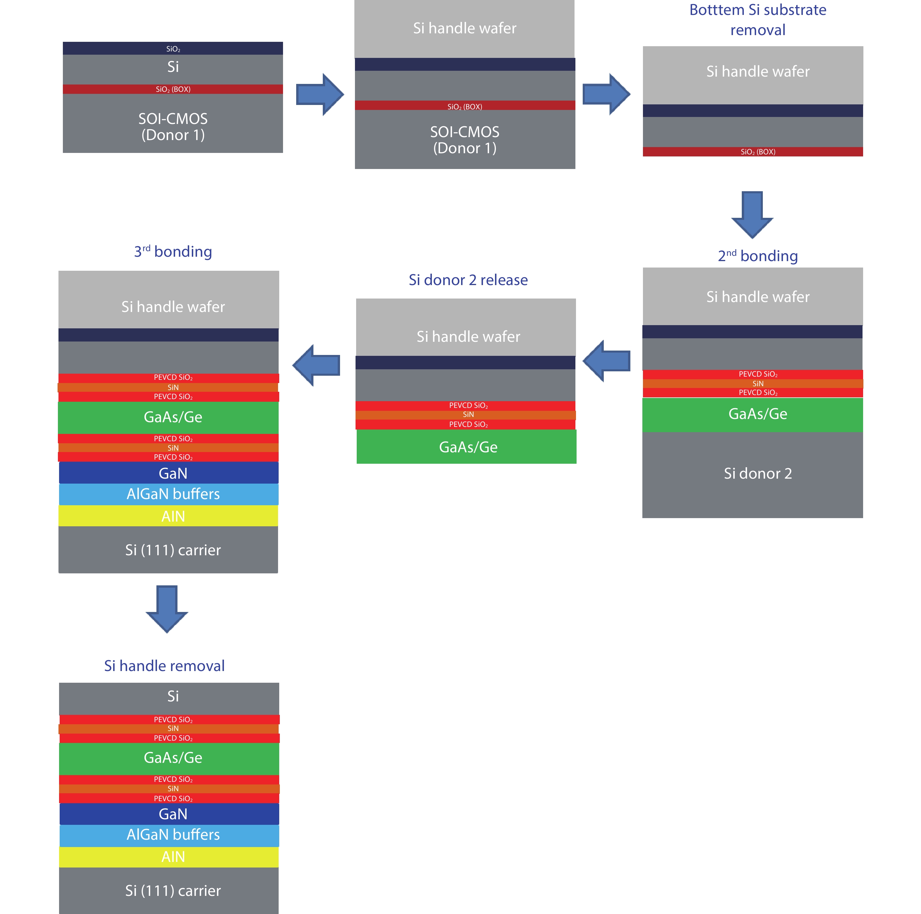
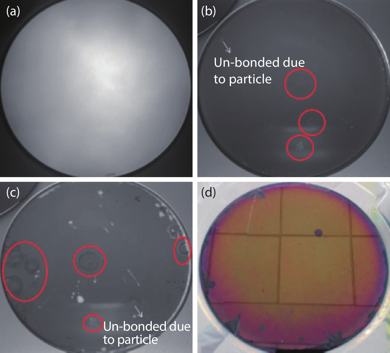
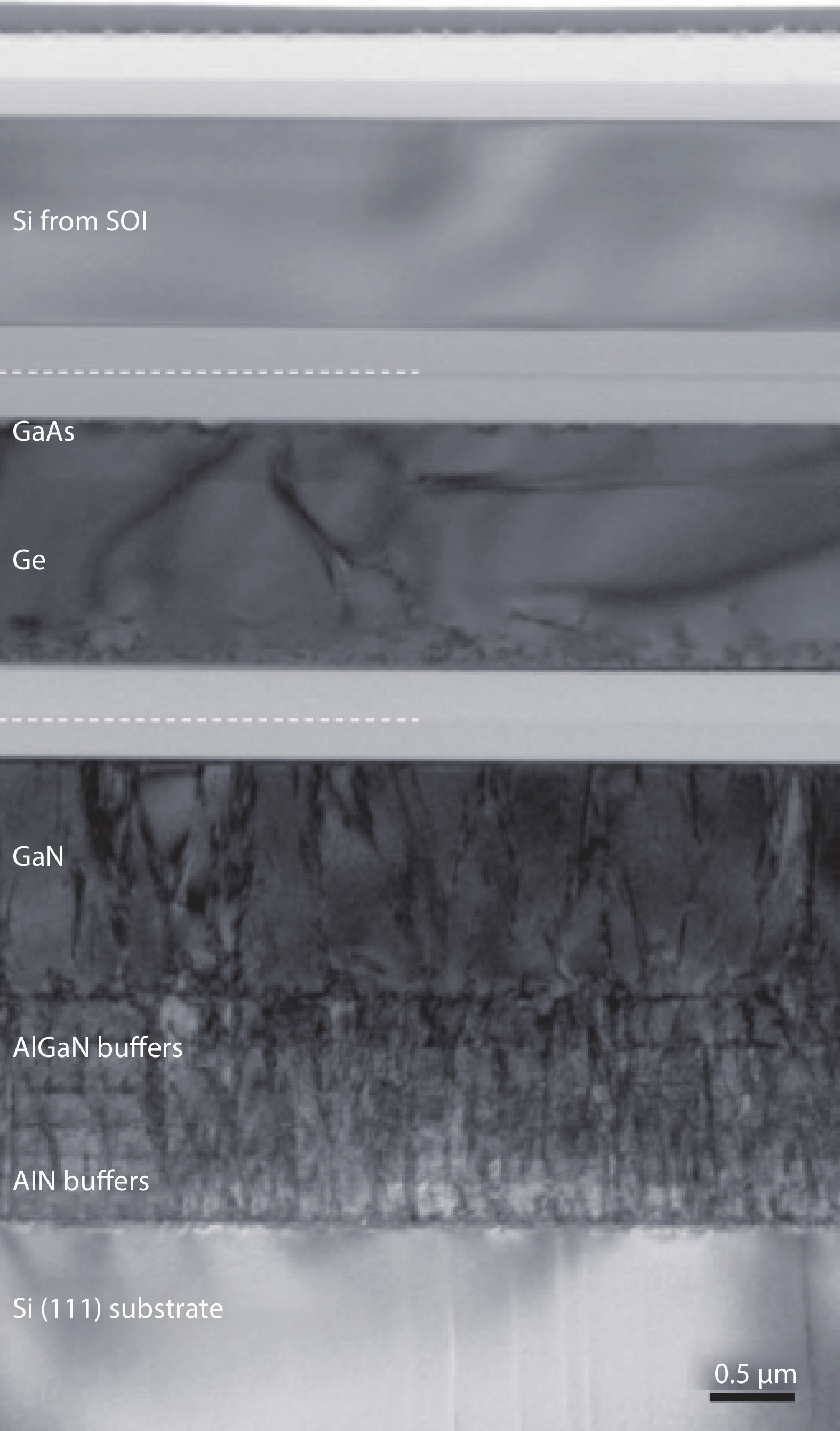
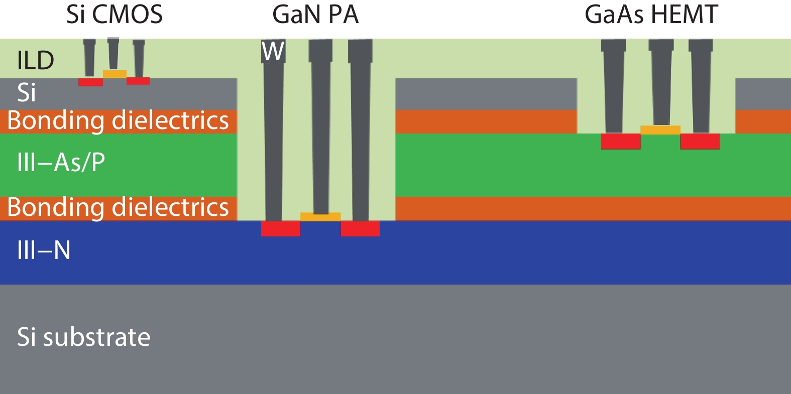
The heterogeneous integration of III–V devices with Si-CMOS on a common Si platform has shown great promise in the new generations of electrical and optical systems for novel applications, such as HEMT or LED with integrated control circuitry. For heterogeneous integration, direct wafer bonding (DWB) techniques can overcome the materials and thermal mismatch issues by directly bonding dissimilar materials systems and device structures together. In addition, DWB can perform at wafer-level, which eases the requirements for integration alignment and increases the scalability for volume production. In this paper, a brief review of the different bonding technologies is discussed. After that, three main DWB techniques of single-, double- and multi-bonding are presented with the demonstrations of various heterogeneous integration applications. Meanwhile, the integration challenges, such as micro-defects, surface roughness and bonding yield are discussed in detail.


J. Semicond.
2021, 42(2): 024102 doi: 10.1088/1674-4926/42/2/024102
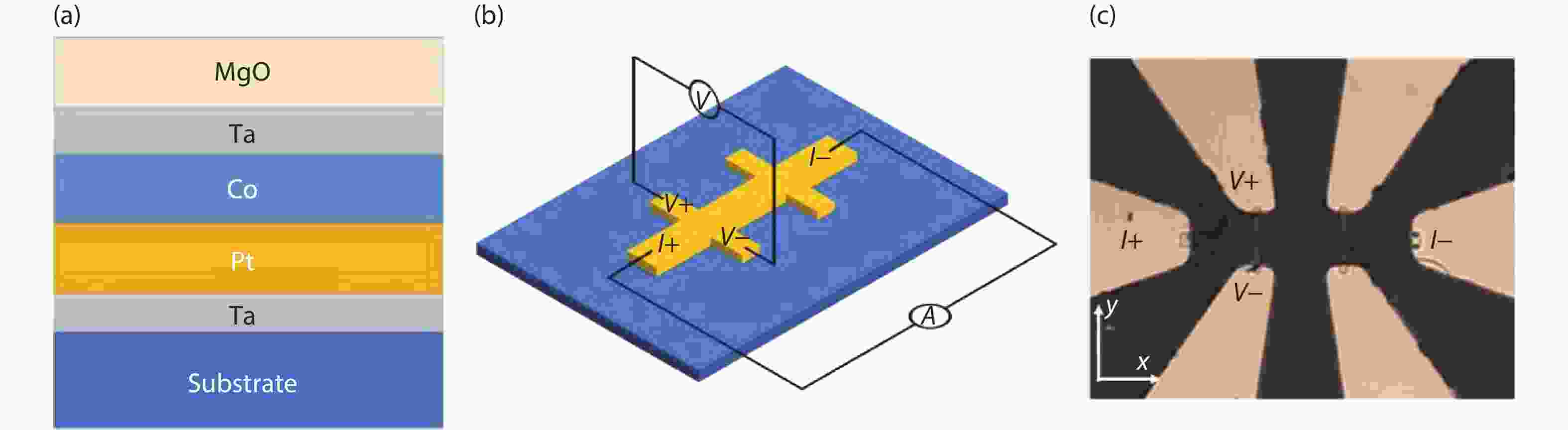
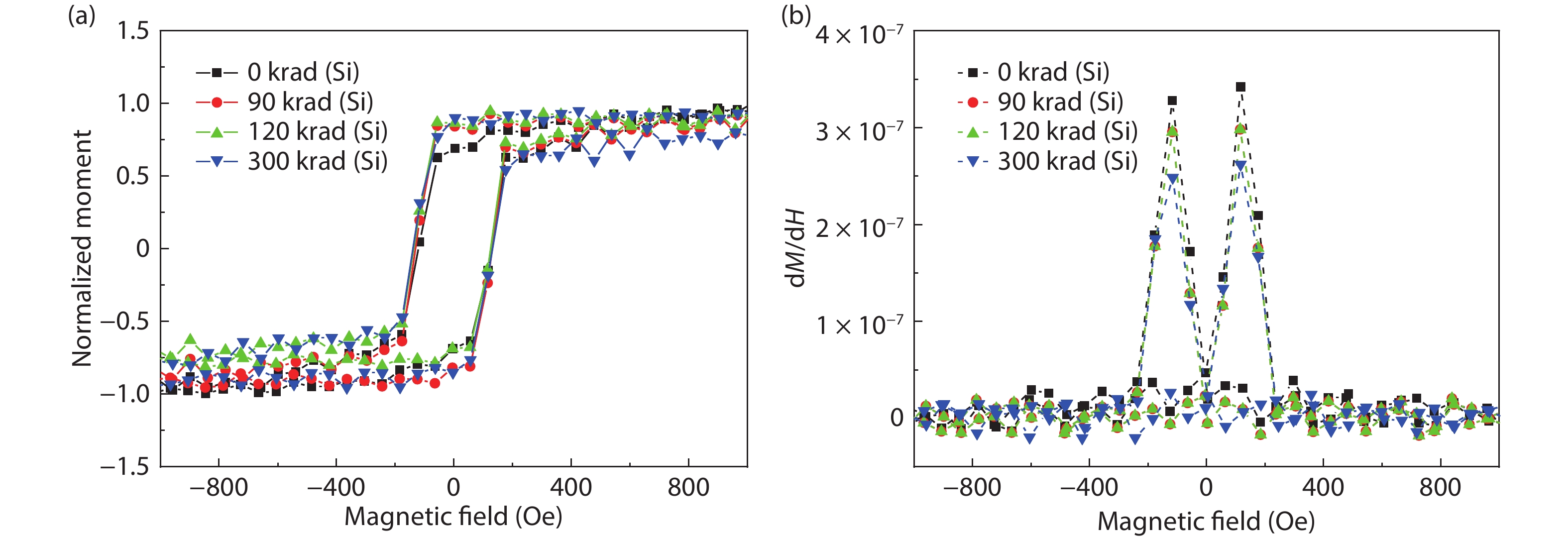
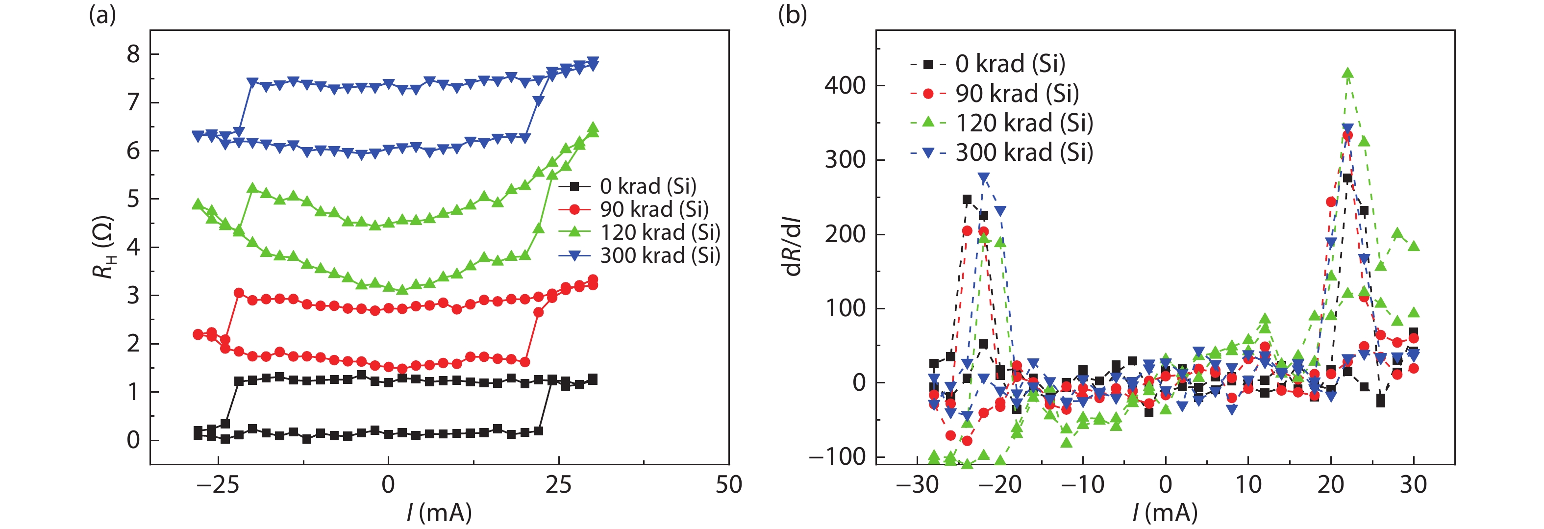
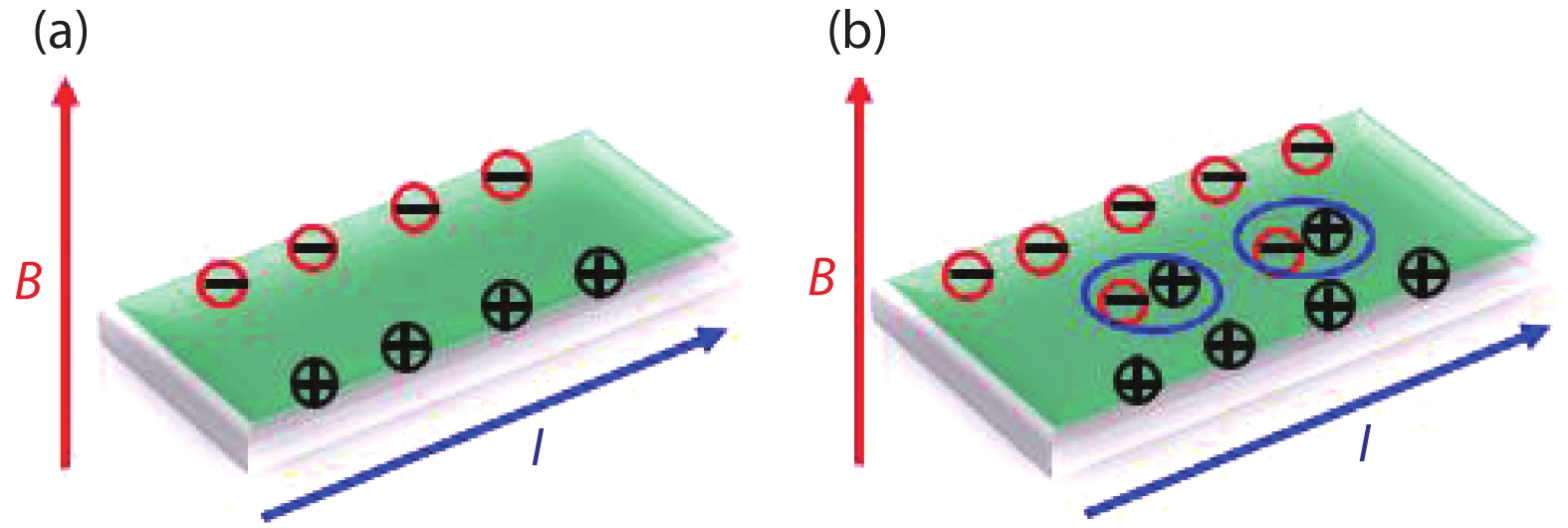
Magnetoresistive random access memories (MRAMs) have drawn the attention of radiation researchers due to their potential high radiation tolerance. In particular, spin-orbit torque MRAM (SOT-MRAM) has the best performance on endurance and access speed, which is considered to be one of the candidates to replace SRAM for space application. However, little attention has been given to the γ-ray irradiation effect on the SOT-MRAM device yet. Here, we report the Co-60 irradiation results for both SOT (spin-orbit torque) magnetic films and SOT-Hall devices with the same stacks. The properties of magnetic films are not affected by radiation even with an accumulated dose up to 300 krad (Si) while the magnetoelectronic properties of SOT-Hall devices exhibit a reversible change behavior during the radiation. We propose a non-equilibrium anomalous Hall effect model to understand the phenomenon. Achieved results and proposed analysis in this work can be used for the material and structure design of memory cell in radiation-hardened SOT-MRAM.
J. Semicond.
2021, 42(2): 024103 doi: 10.1088/1674-4926/42/2/024103
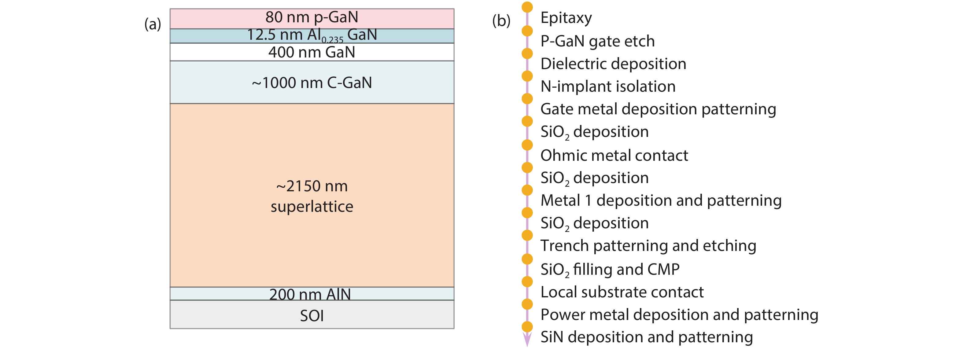
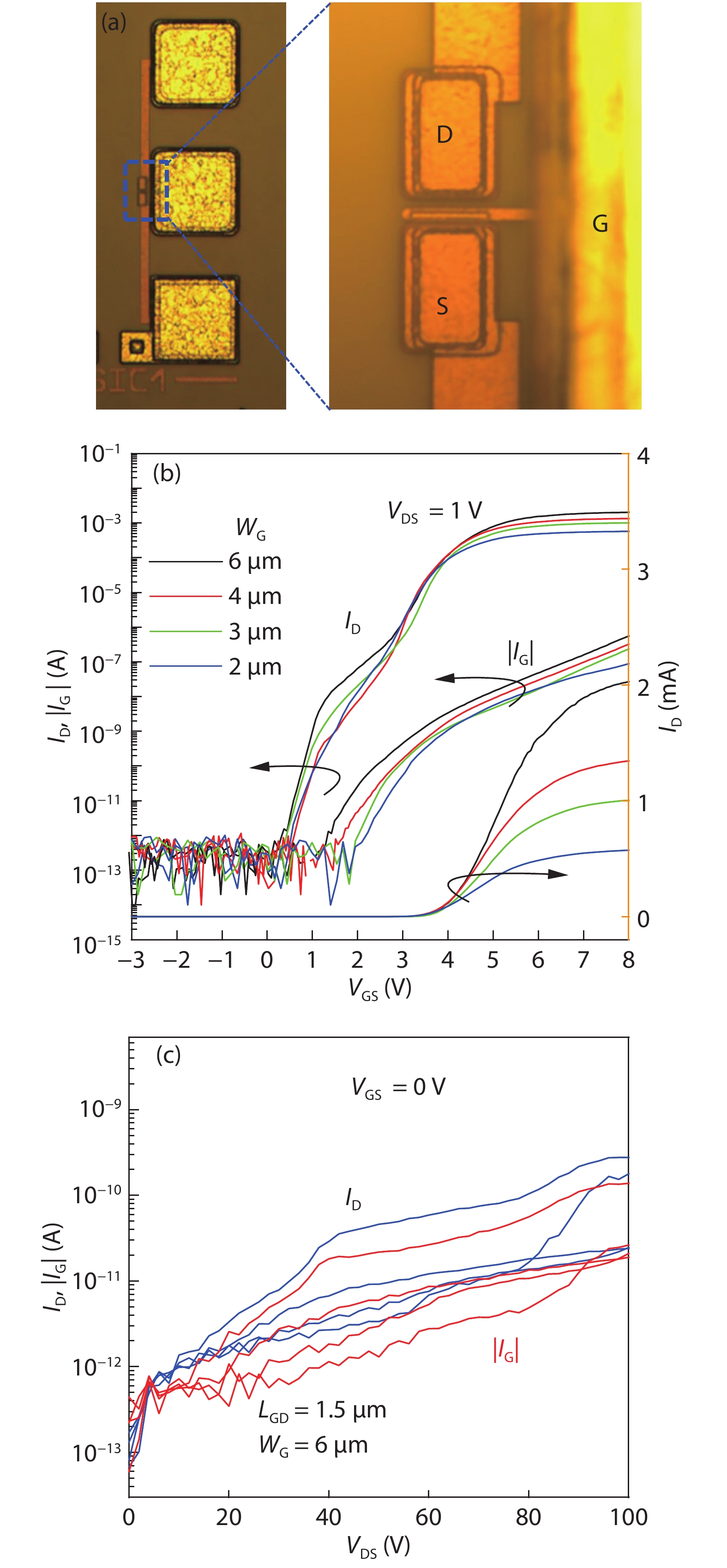
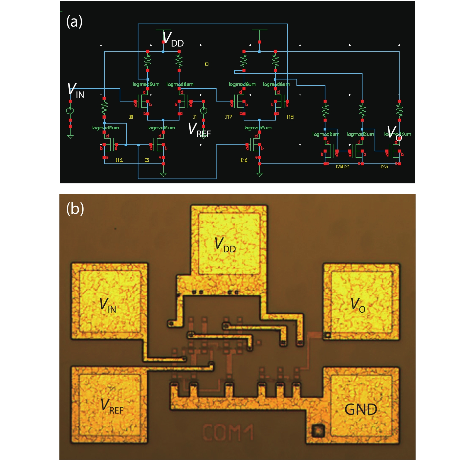
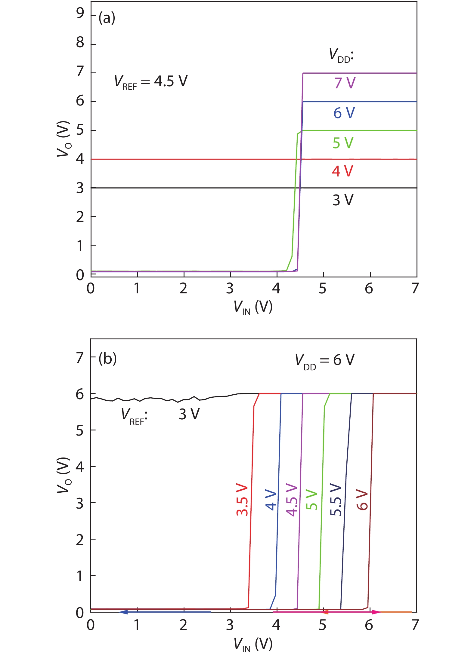
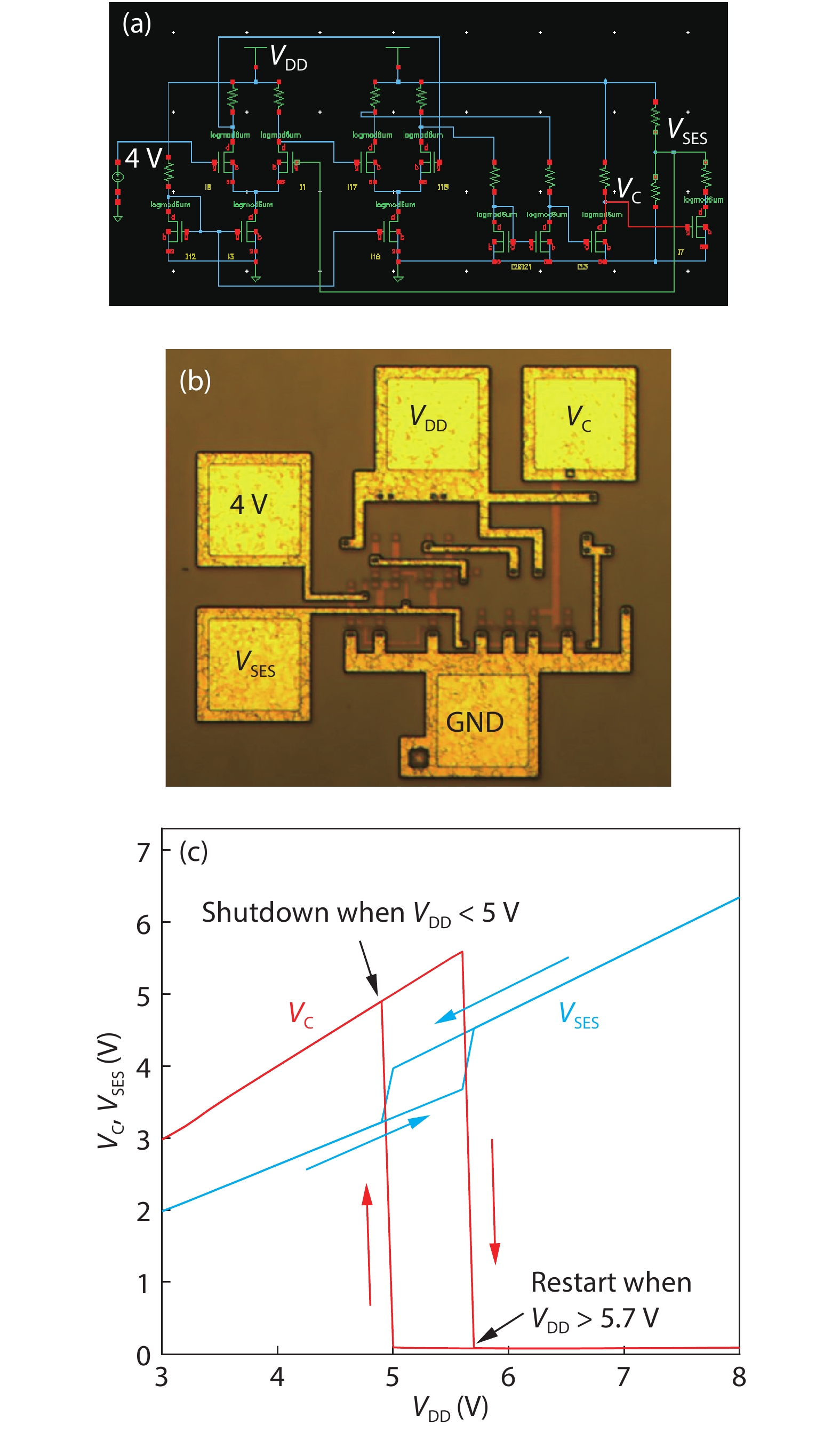
We demonstrate the key module of comparators in GaN ICs, based on resistor-transistor logic (RTL) on E-mode wafers in this work. The fundamental inverters in the comparator consist of a p-GaN gate HEMT and a 2DEG resistor as the load. The function of the RTL comparators is finally verified by a undervoltage lockout (UVLO) circuit. The compatibility of this circuit with the current p-GaN technology paves the way for integrating logic ICs together with the power devices.

J. Semicond.
2021, 42(2): 024101 doi: 10.1088/1674-4926/42/2/024101
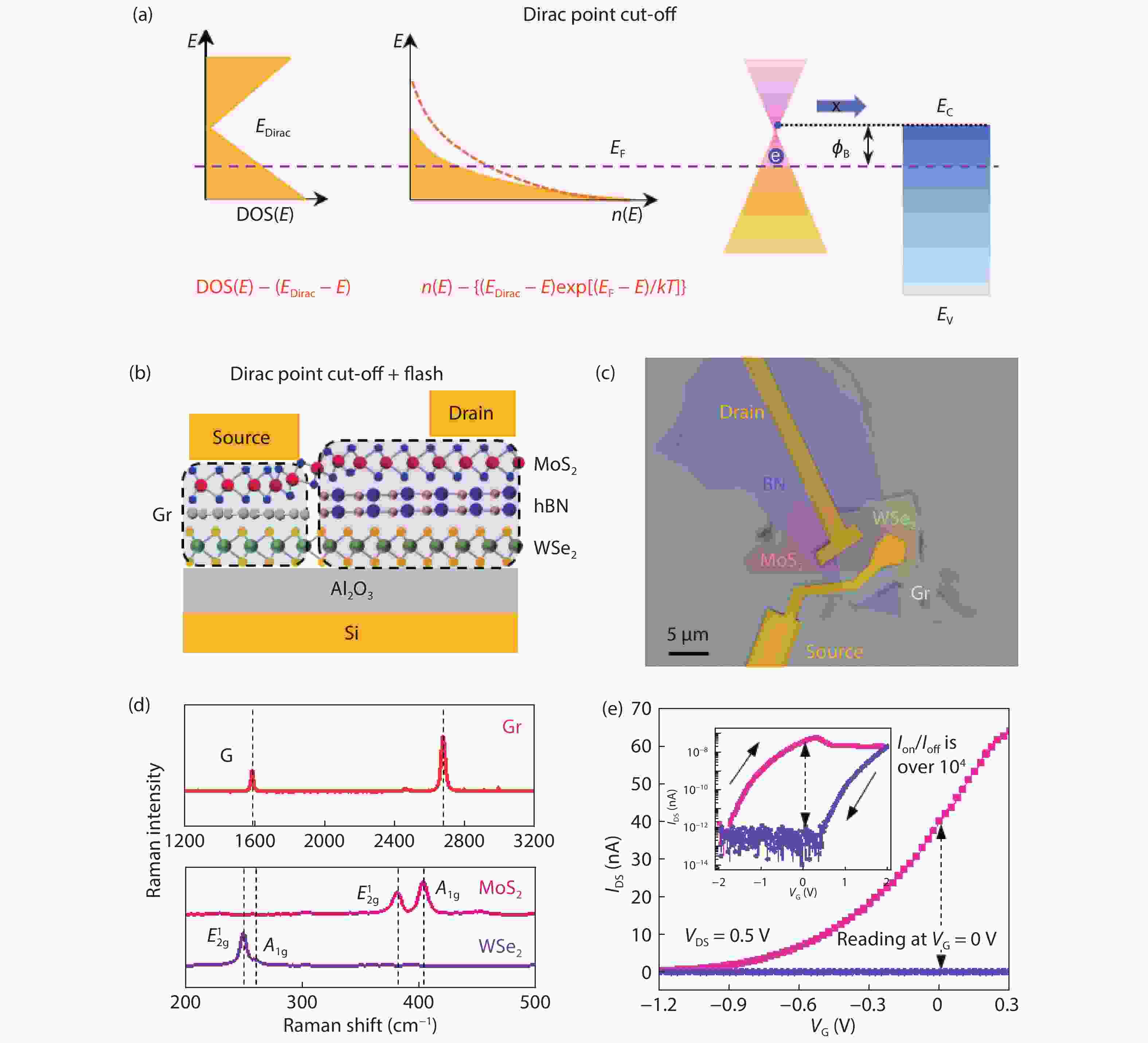
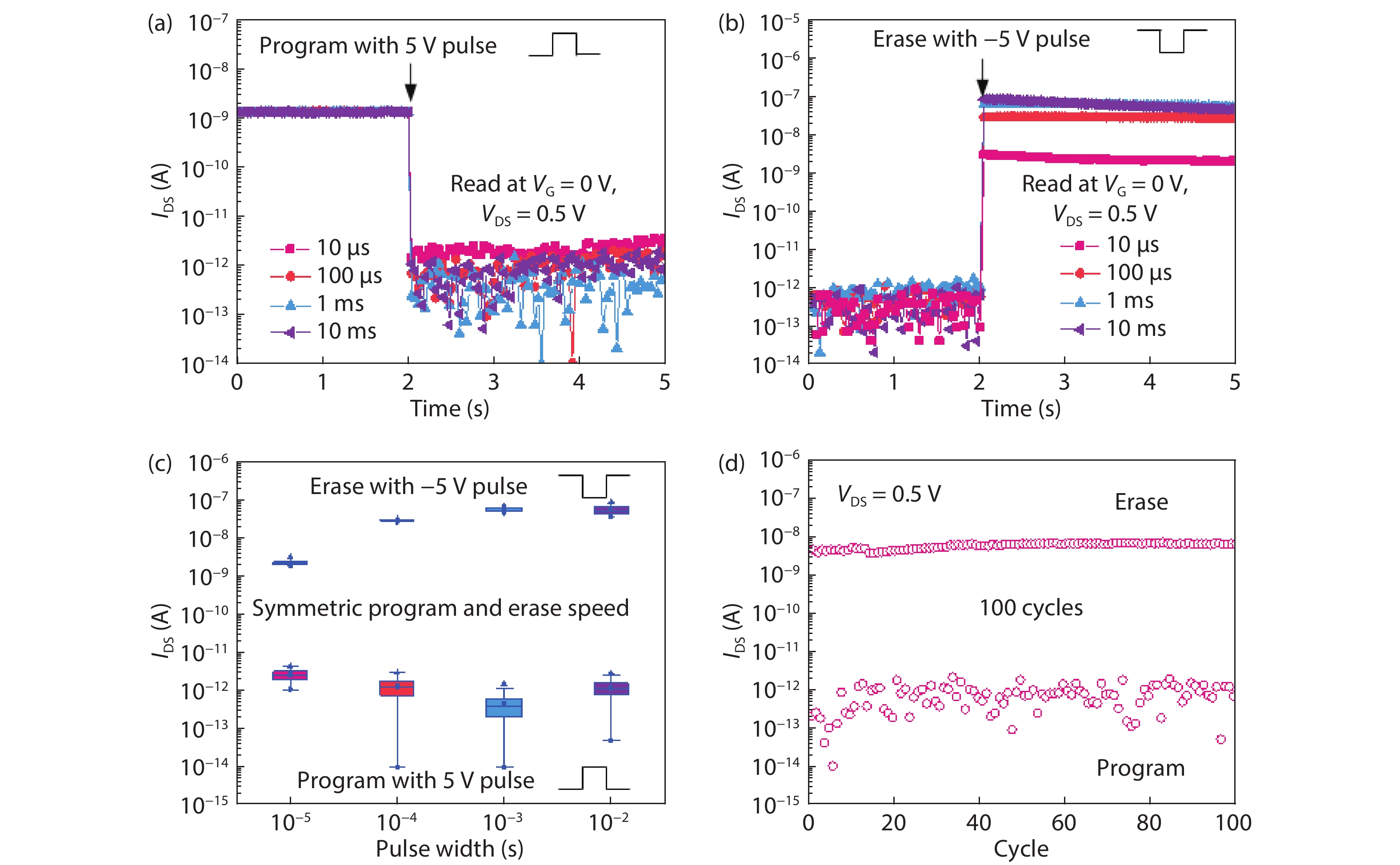
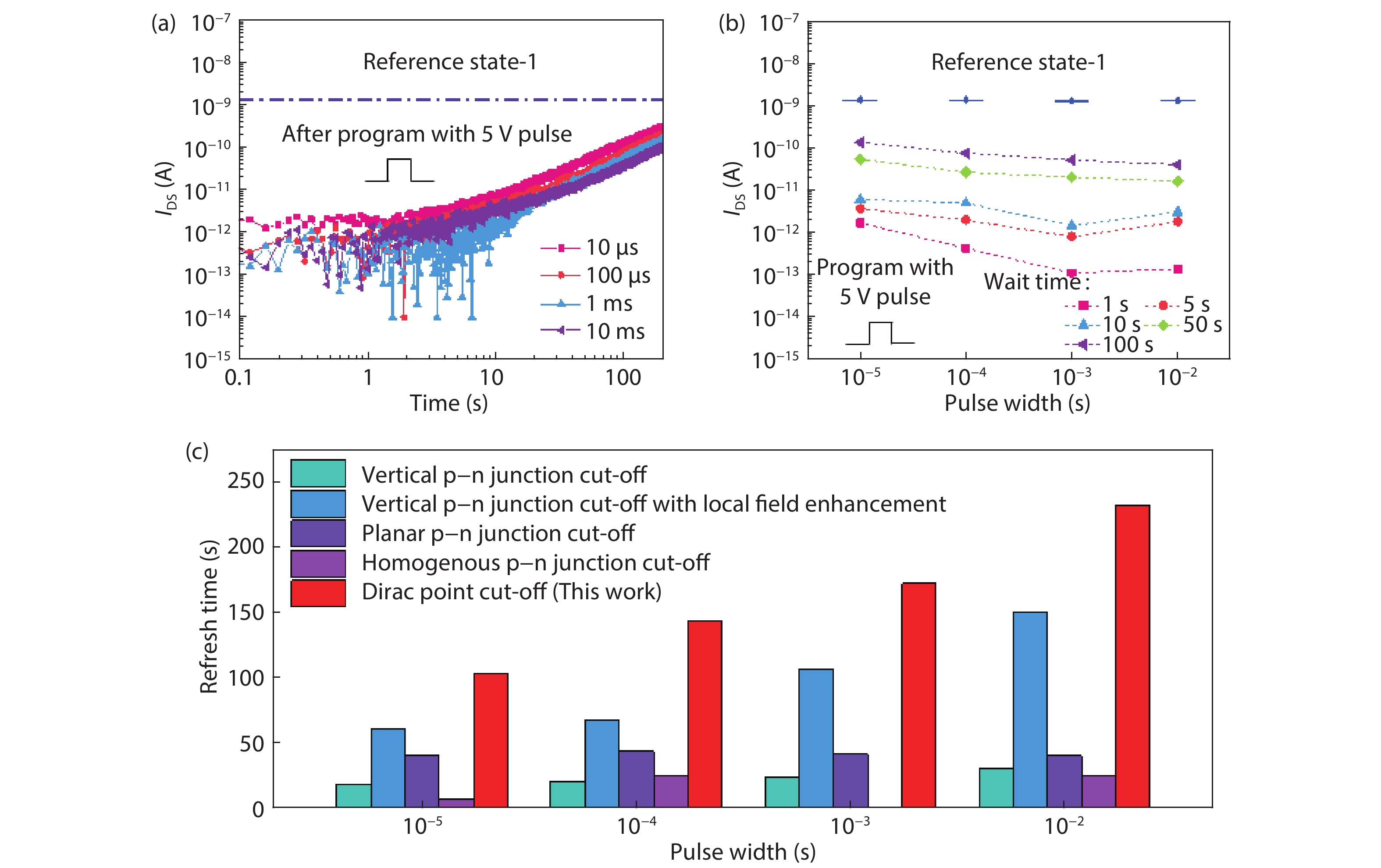
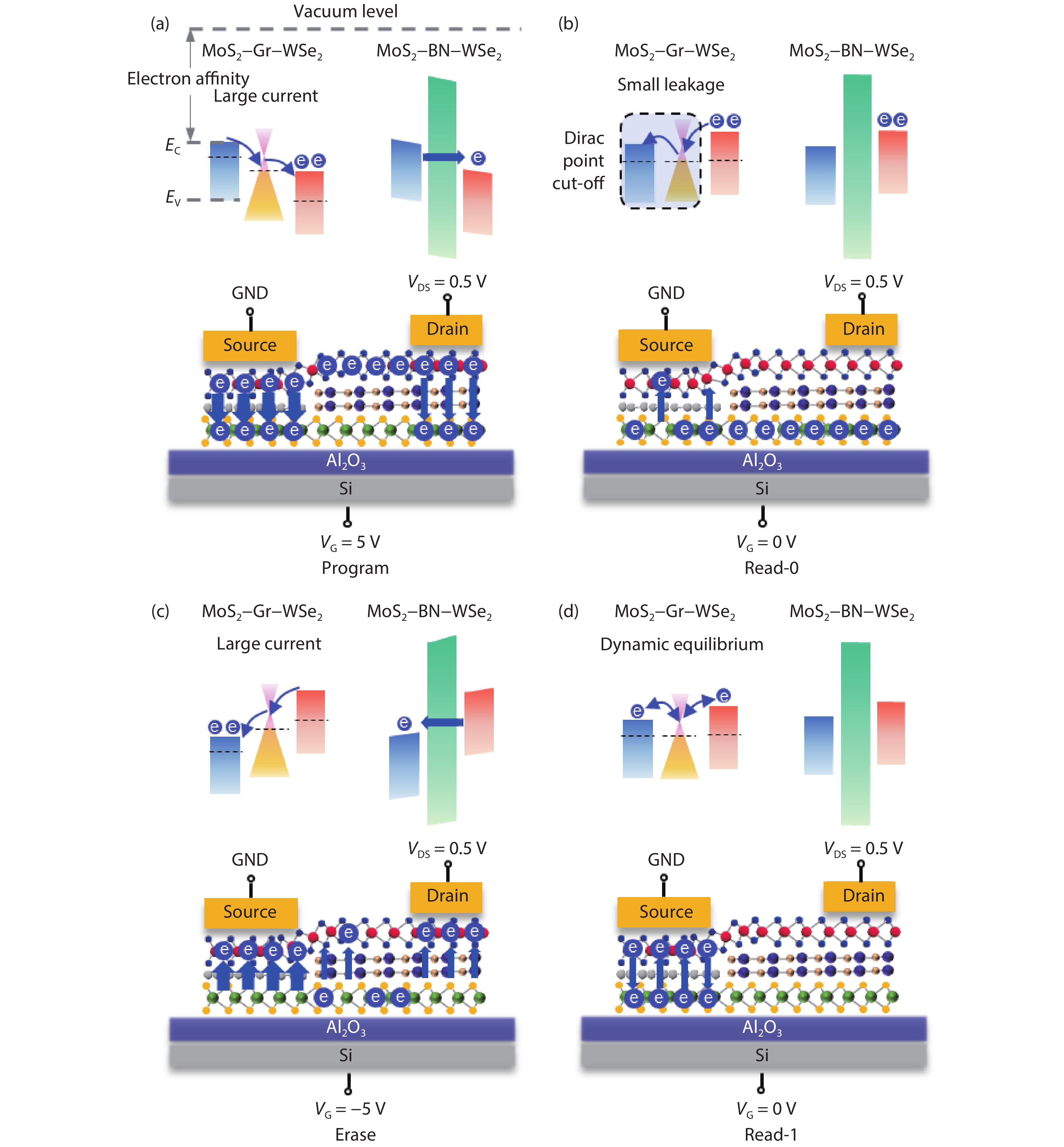
The recently reported quasi-nonvolatile memory based on semi-floating gate architecture has attracted extensive attention thanks to its potential to bridge the large gap between volatile and nonvolatile memory. However, the further extension of the refresh time in quasi-nonvolatile memory is limited by the charge leakage through the p–n junction. Here, based on the density of states engineered van der Waals heterostructures, the leakage of electrons from the floating gate to the channel is greatly suppressed. As a result, the refresh time is effectively extended to more than 100 s, which is the longest among all previously reported quasi-nonvolatile memories. This work provides a new idea to enhance the refresh time of quasi-nonvolatile memory by the density of states engineering and demonstrates great application potential for high-speed and low-power memory technology.