Issue Browser
Volume 43, Issue 5,
May 2022


J. Semicond.
2022, 43(5): 051201 doi: 10.1088/1674-4926/43/5/051201
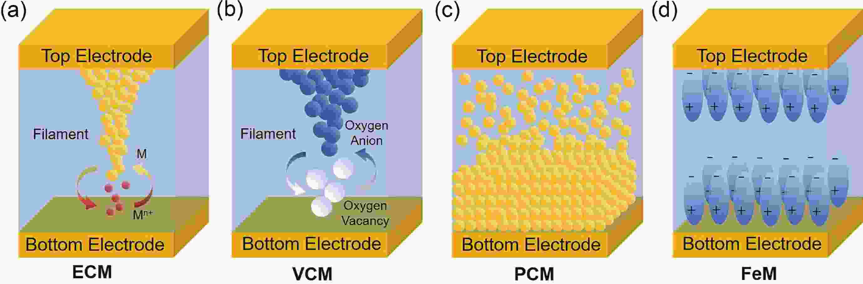
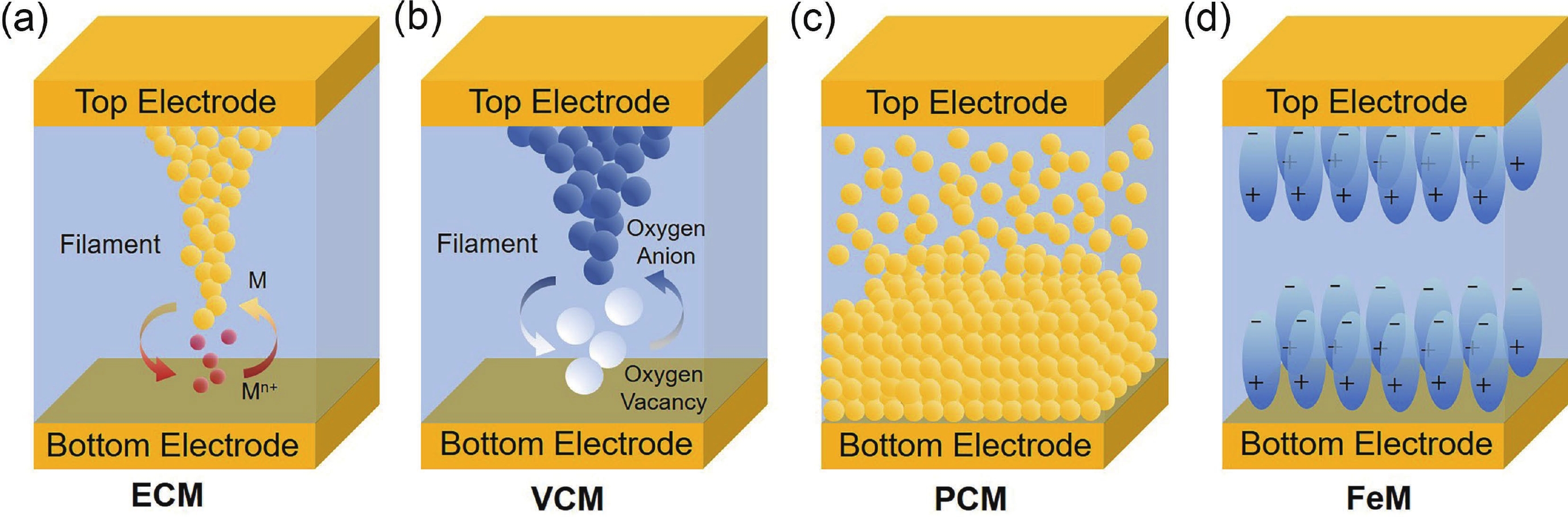
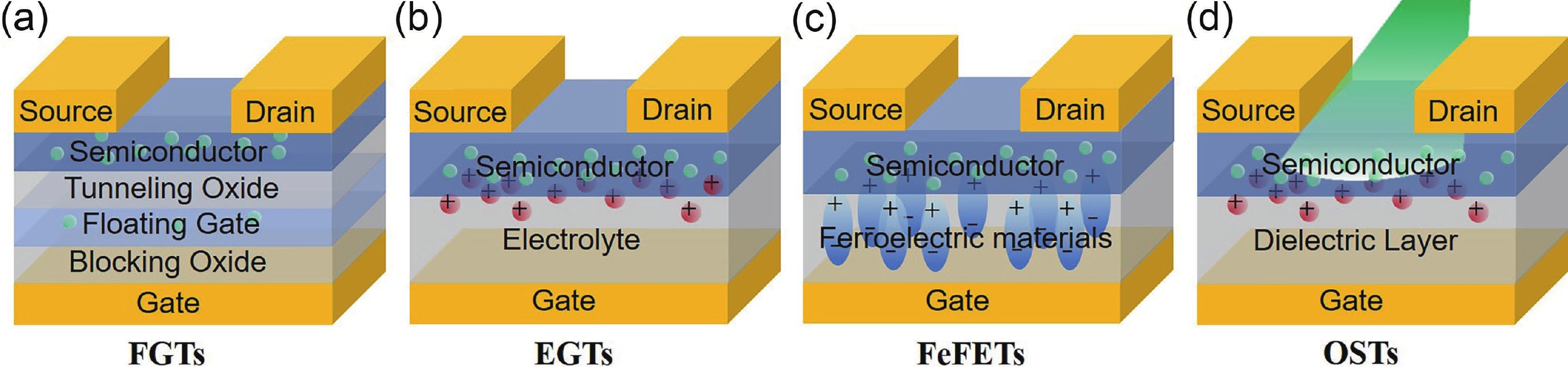
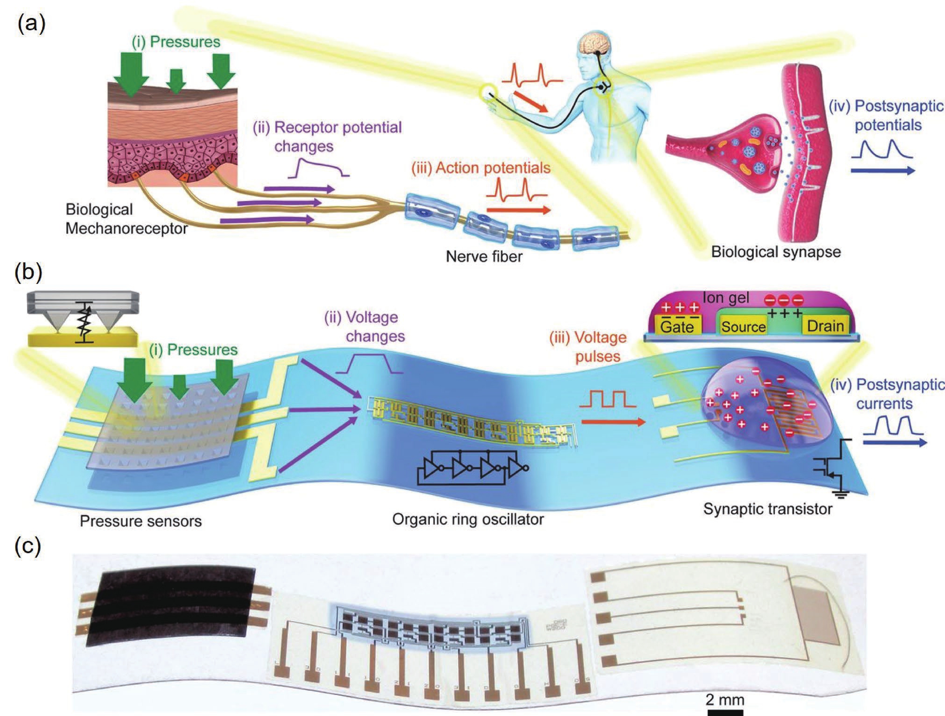
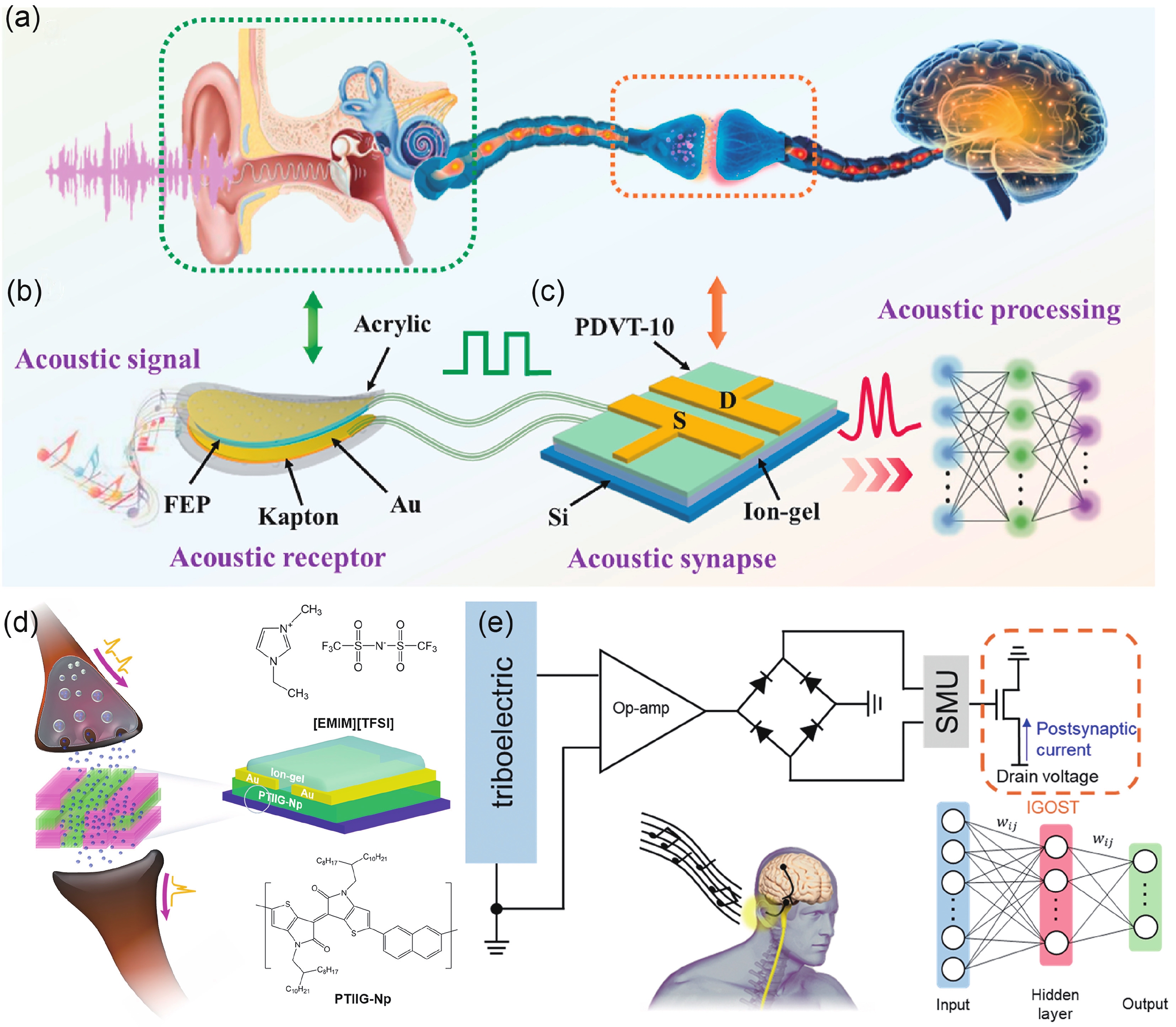
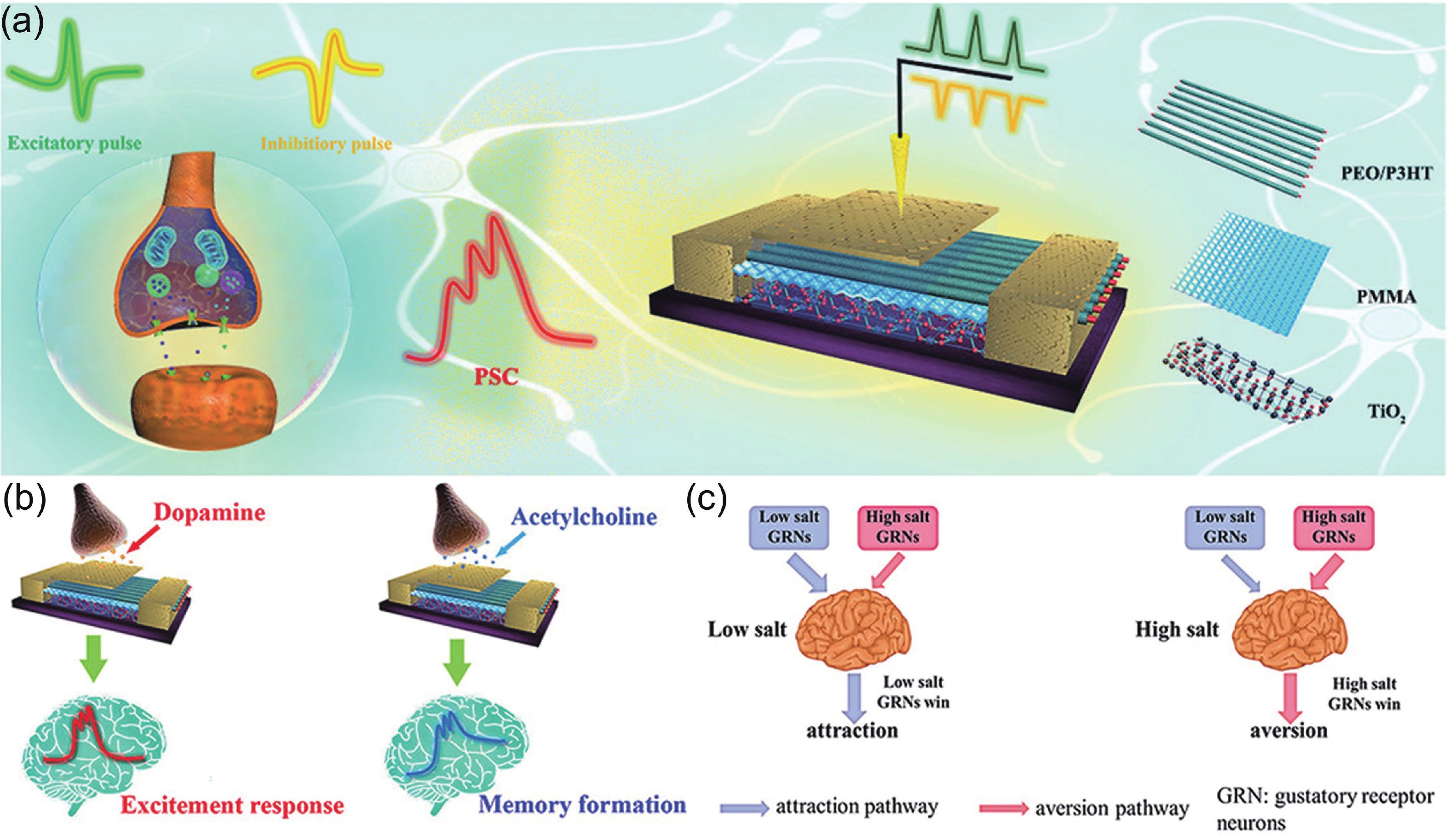
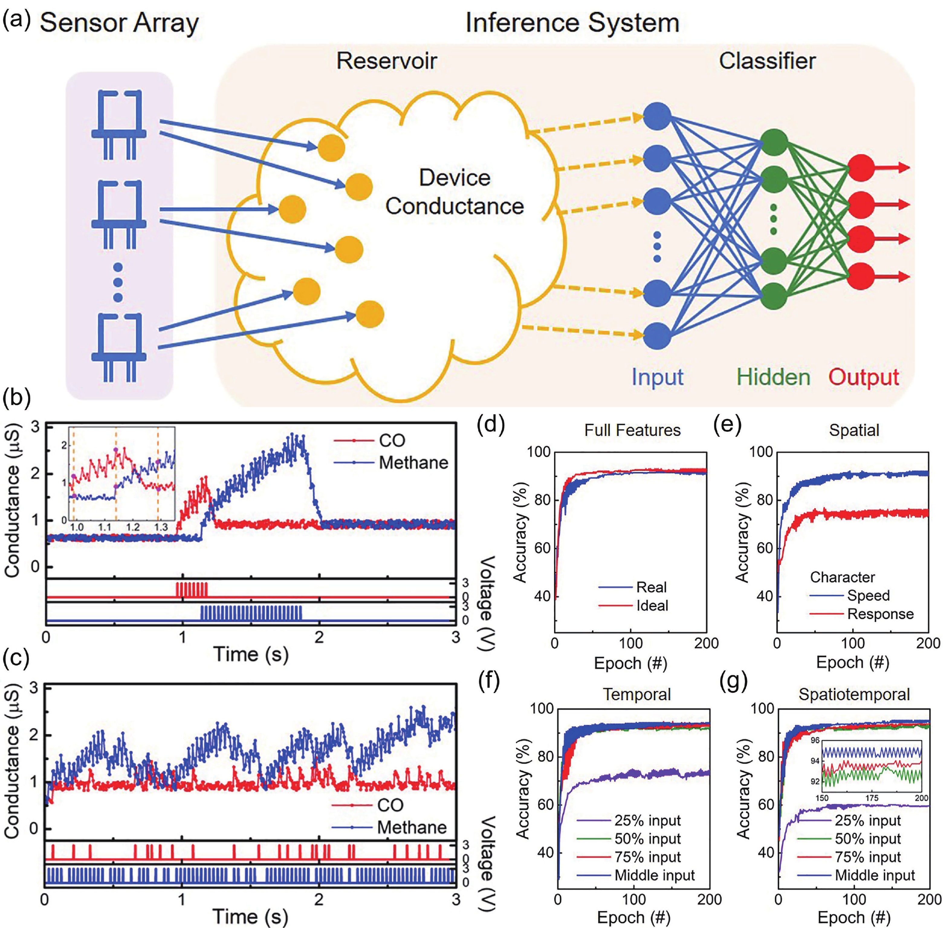
The traditional Von Neumann architecture for processing information is difficult to meet the needs of the big data era, while low-power, small-sized neurosynaptic devices can operate and store information, so that they have received extensive attention. Due to the development of artificial intelligence and robotics, neurosynaptic devices have been given high expectations and requirements. The trend of functionalization, intelligence, and integration of computing and storage is obvious. In this review, the basic principles and types of neurosynaptic devices are summarized, the achievements of neurosynaptic devices for human perception systems are discussed and a prospect on the development trend is also given.


J. Semicond.
2022, 43(5): 051202 doi: 10.1088/1674-4926/43/5/051202

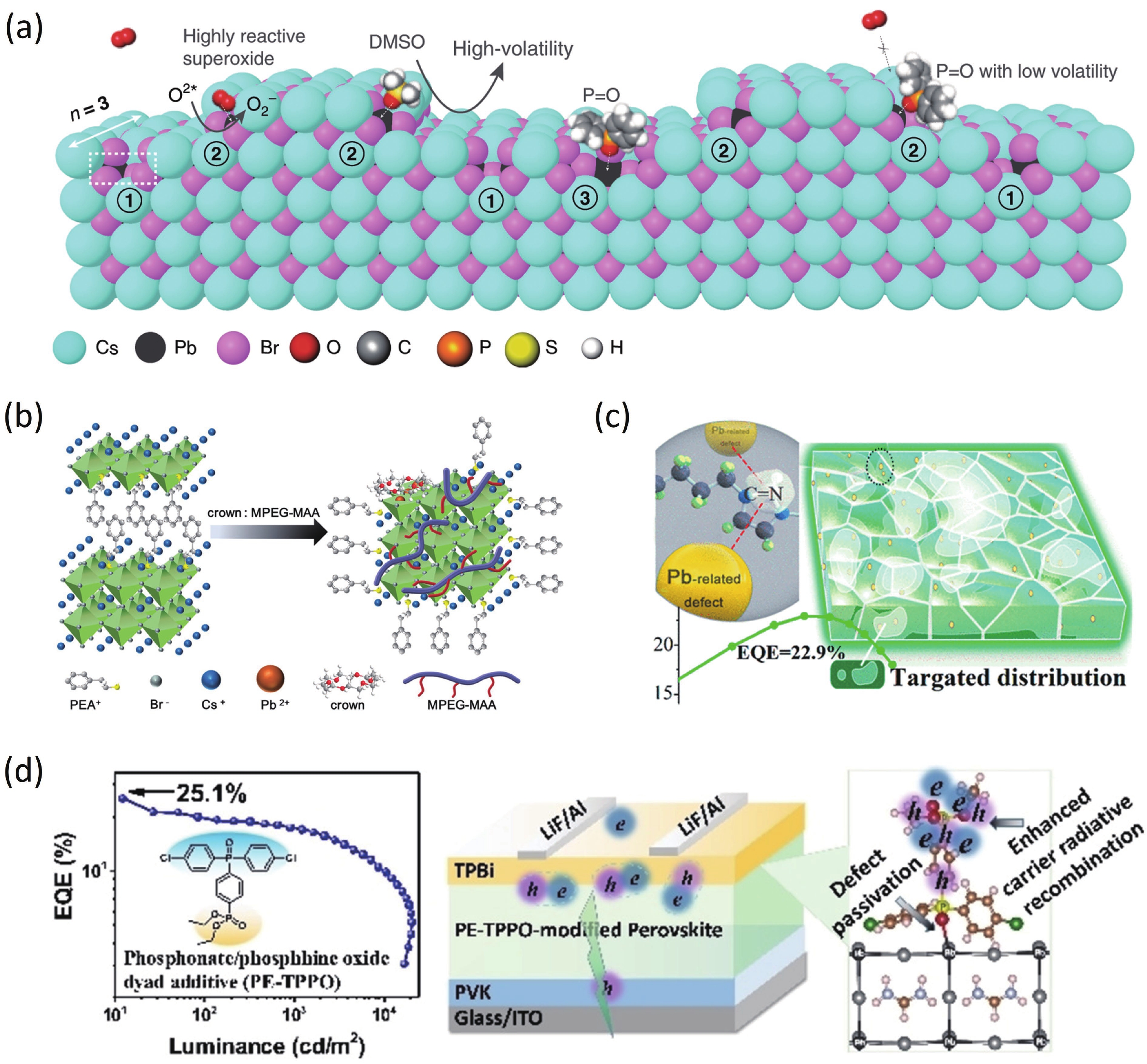
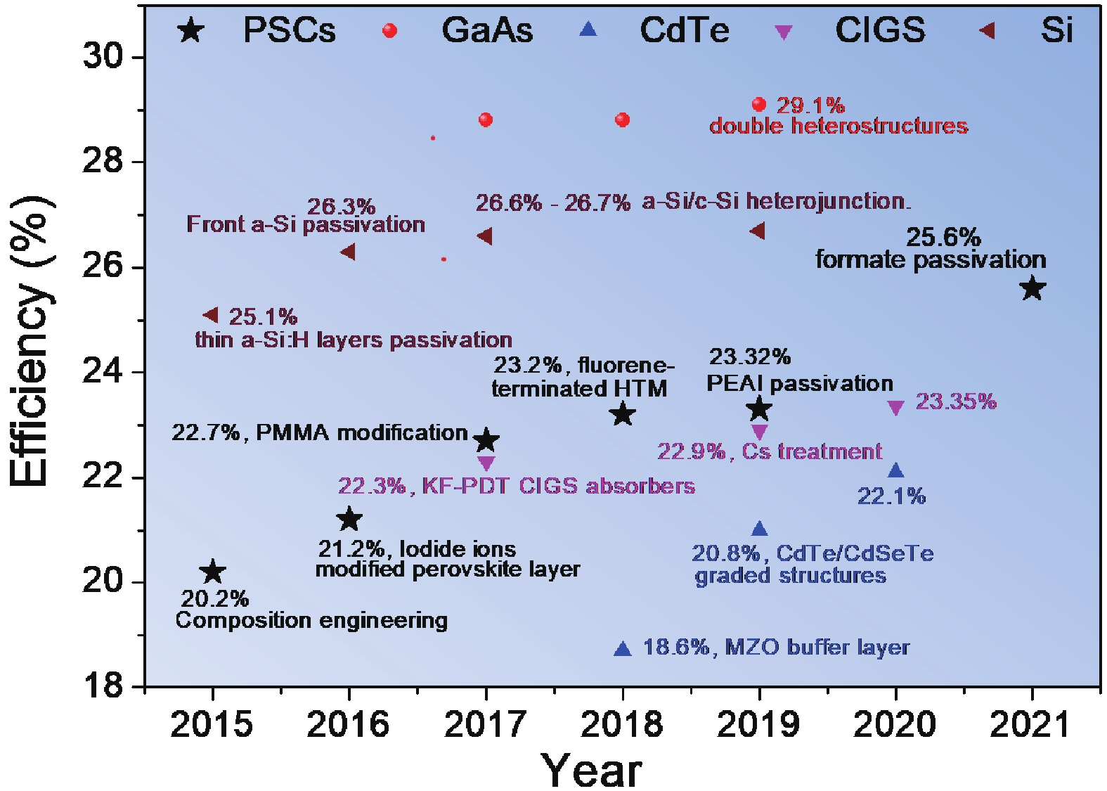
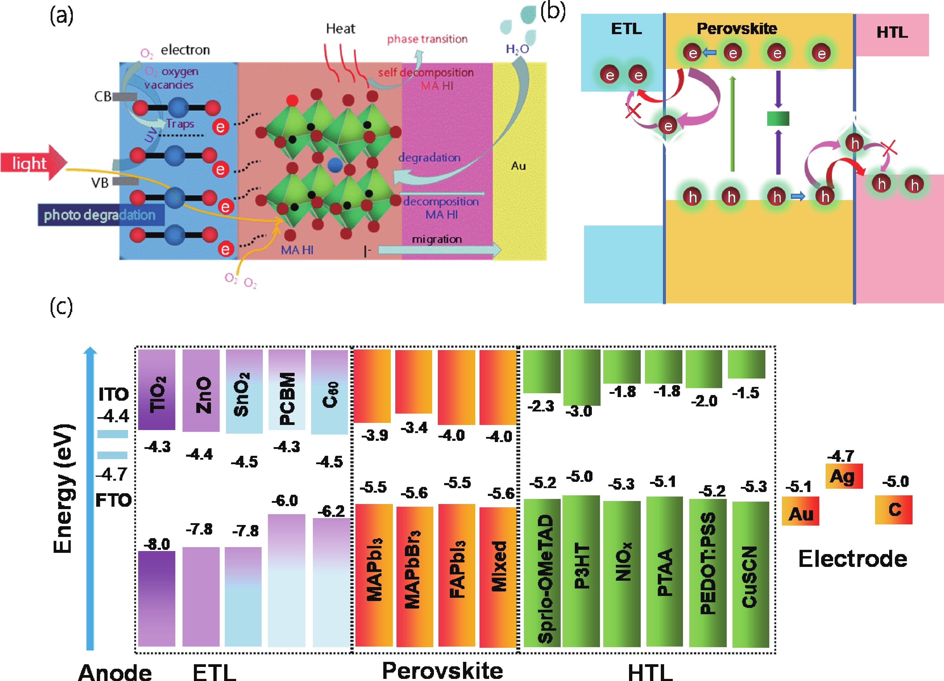
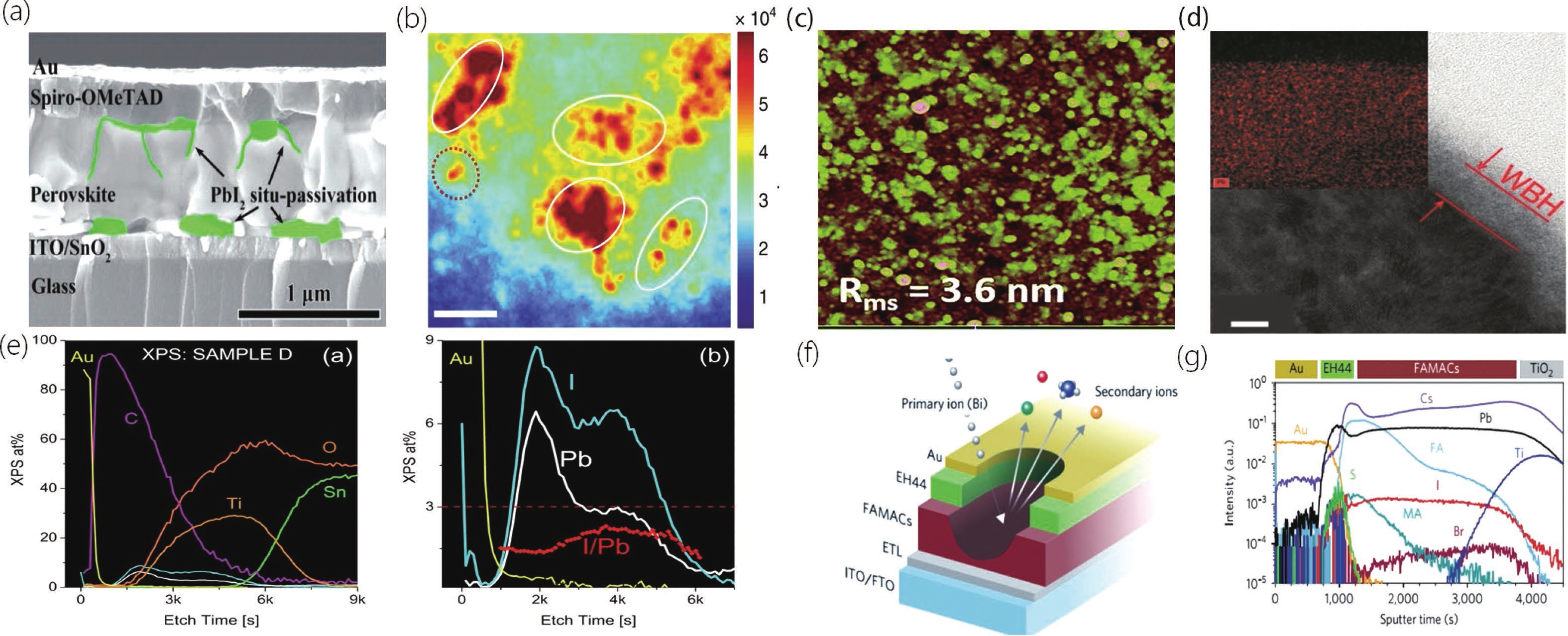
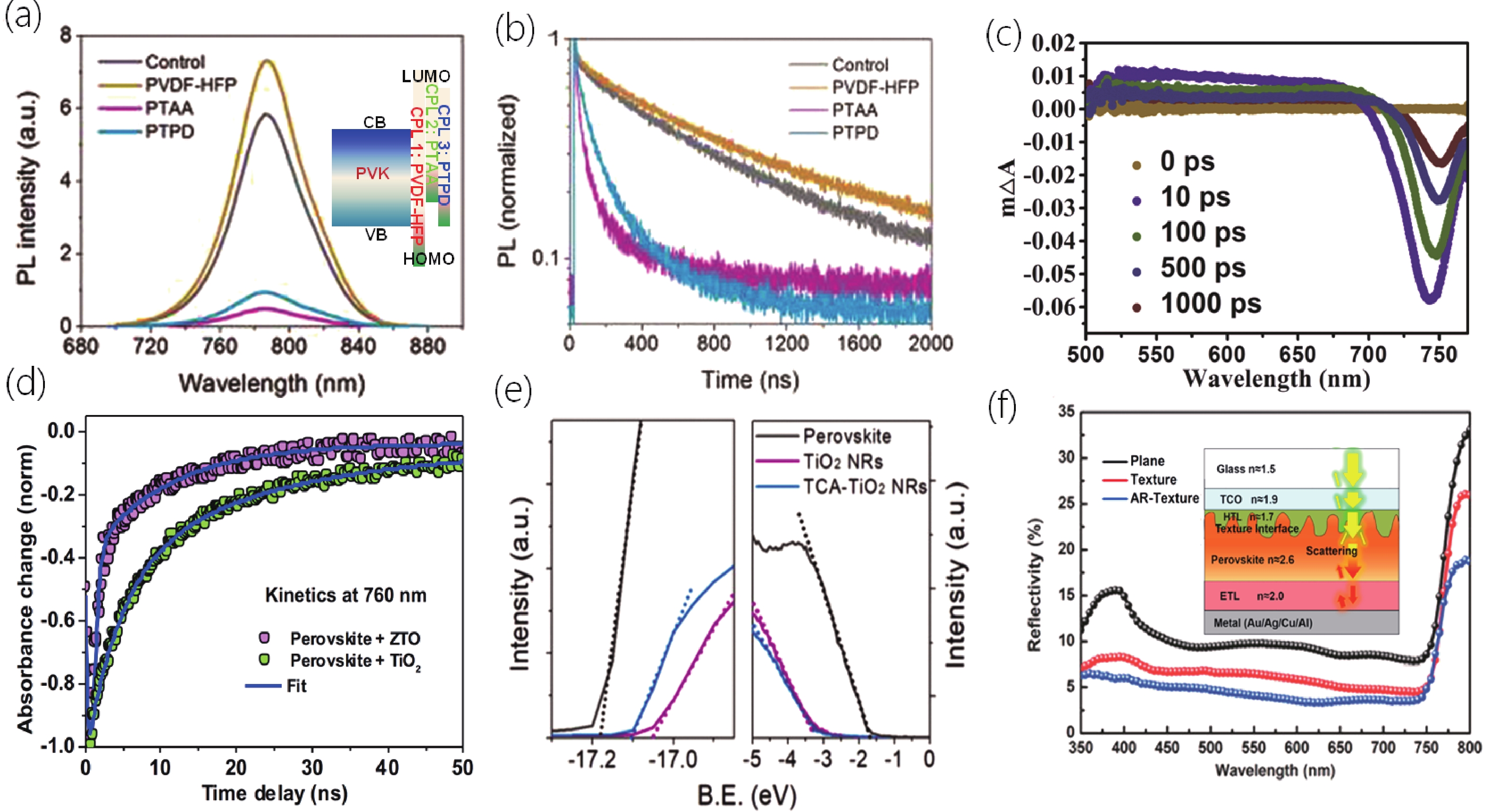
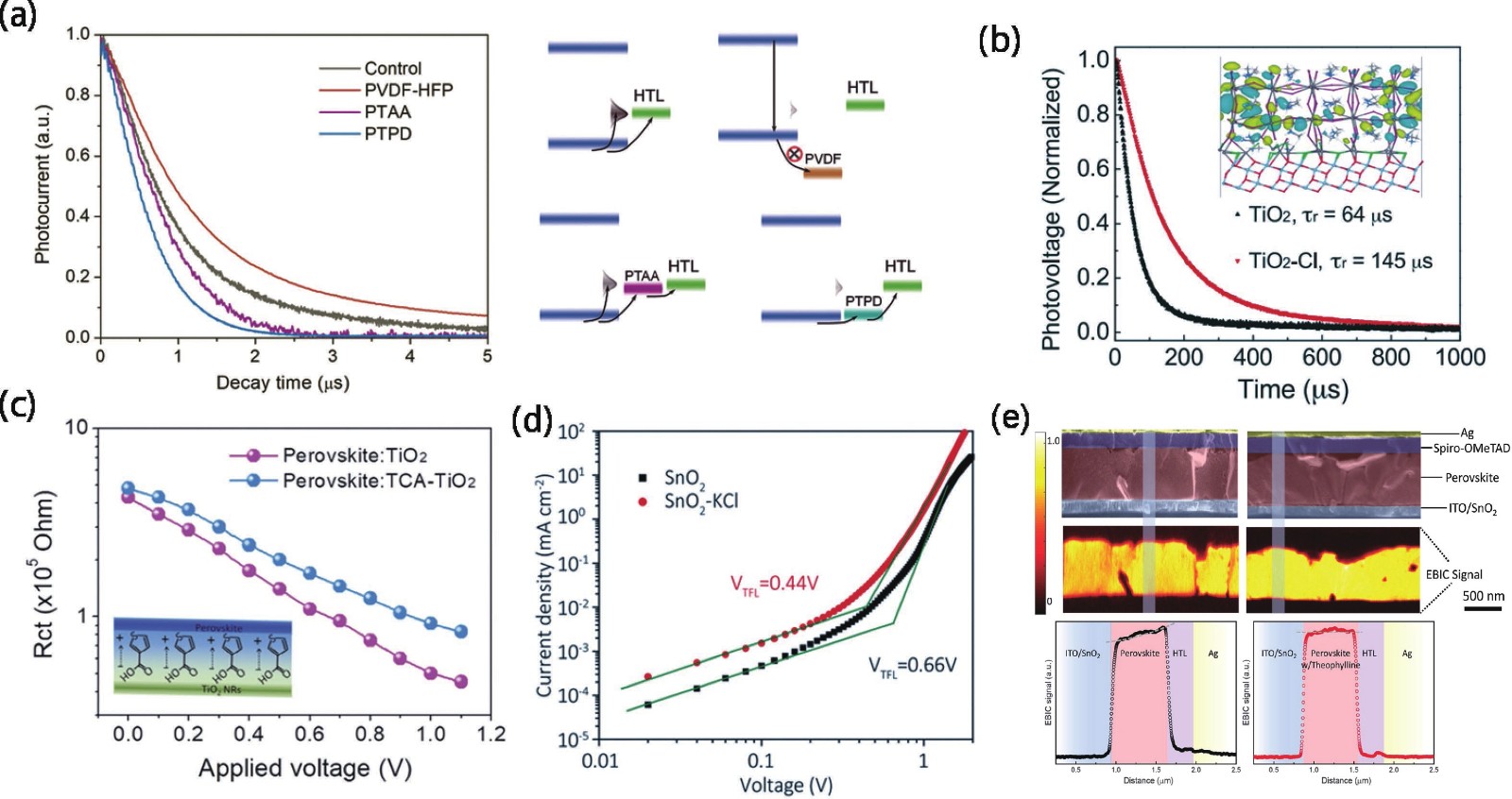
A photovoltaic technology historically goes through two major steps to evolve into a mature technology. The first step involves advances in materials and is usually accompanied by the rapid improvement of power conversion efficiency. The second step focuses on interfaces and is usually accompanied by significant stability improvement. As an emerging generation of photovoltaic technology, perovskite solar cells are transitioning to the second step of their development when a significant focus shifts toward interface studies and engineering. While various interface engineering strategies have been developed, interfacial characterization is crucial to show the effectiveness of interfacial modification. Here, we review the characterization techniques that have been utilized in studying interface properties in perovskite solar cells. We first summarize the main roles of interfaces in perovskite solar cells, and then we discuss some typical characterization methodologies for morphological, optical, and electrical studies of interfaces. Successful experiences and existing problems are analyzed when discussing some commonly used methods. We then analyze the challenges and provide an outlook for further development of interfacial characterizations. This review aims to evoke strengthened research devotion on novel and persuasive interfacial engineering.
J. Semicond.
2022, 43(5): 052002 doi: 10.1088/1674-4926/43/5/052002
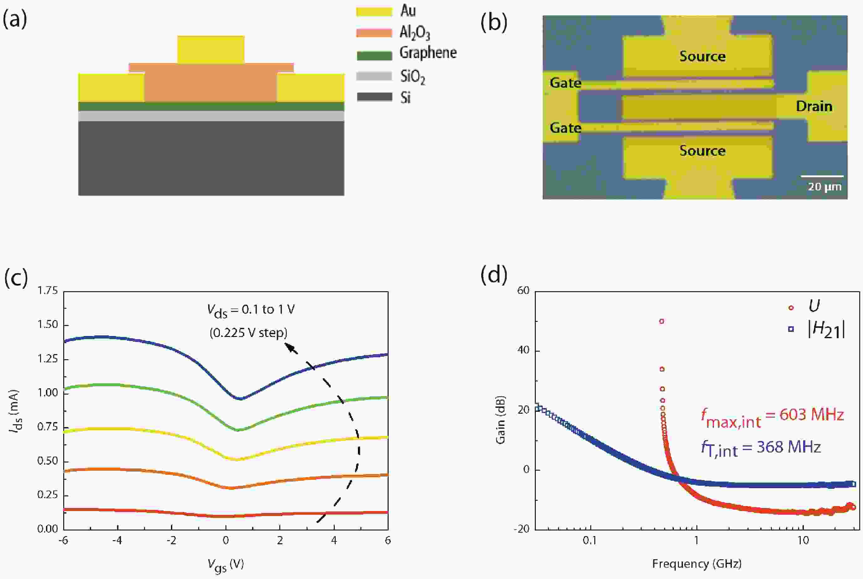
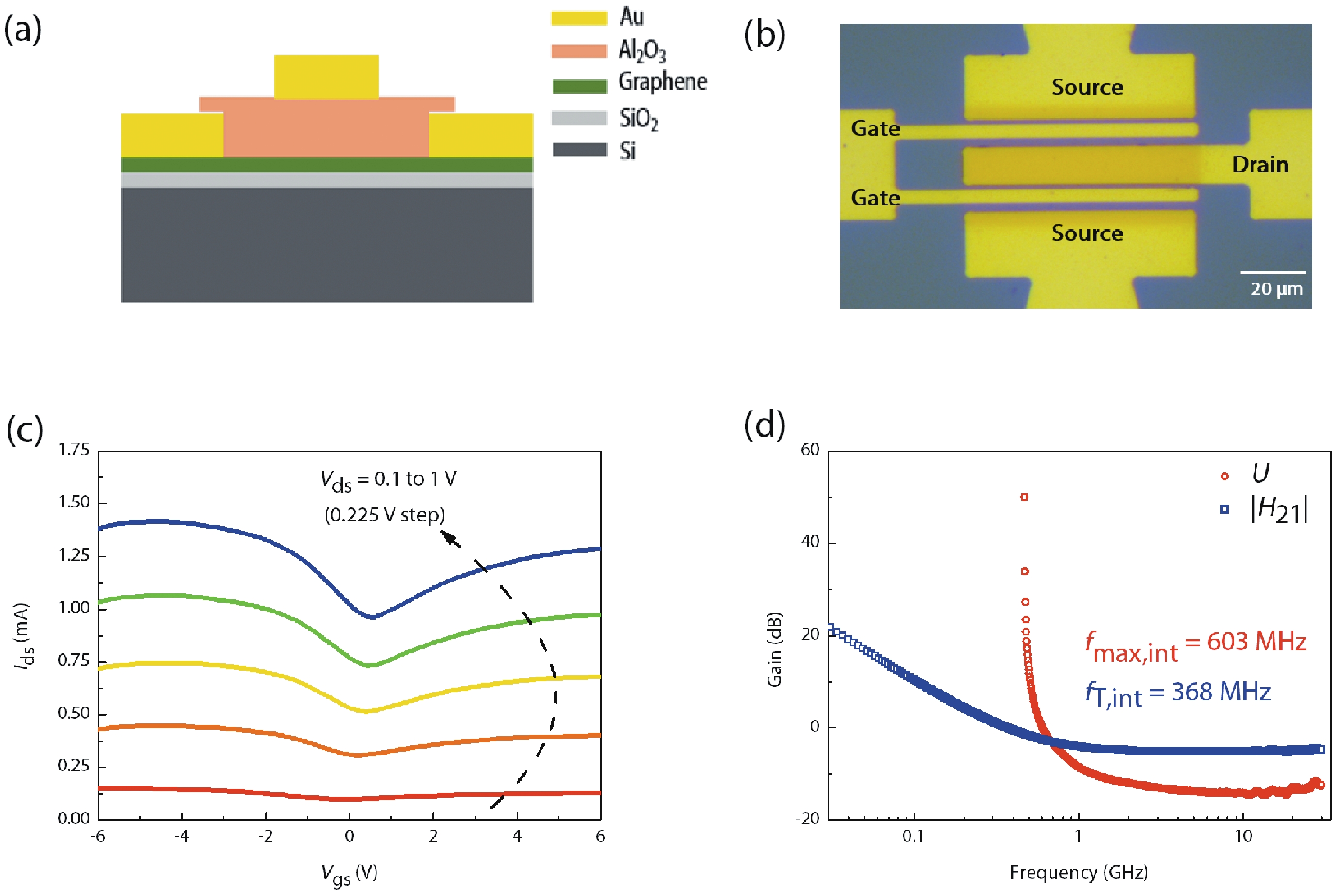
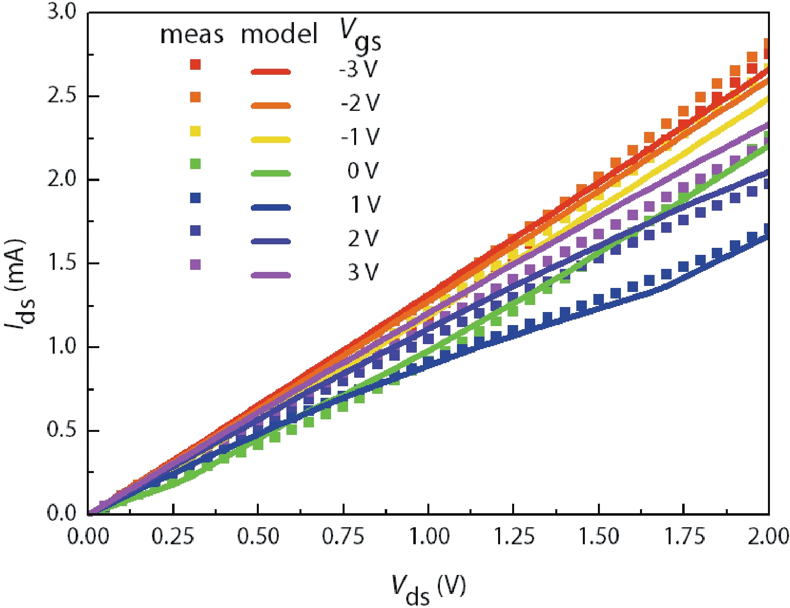
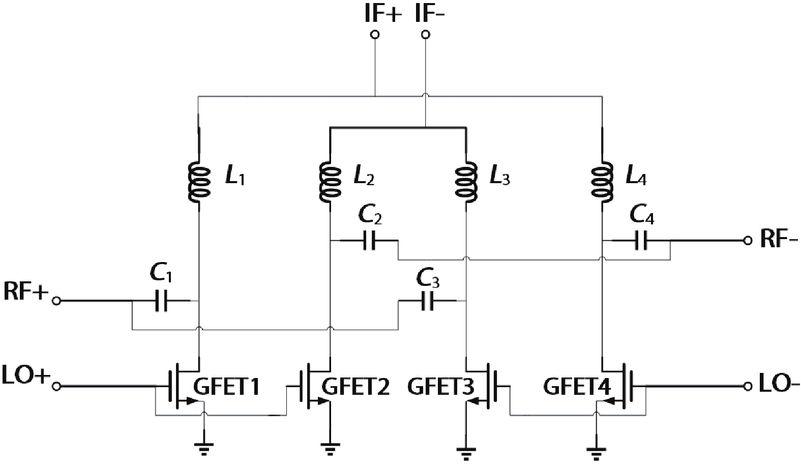
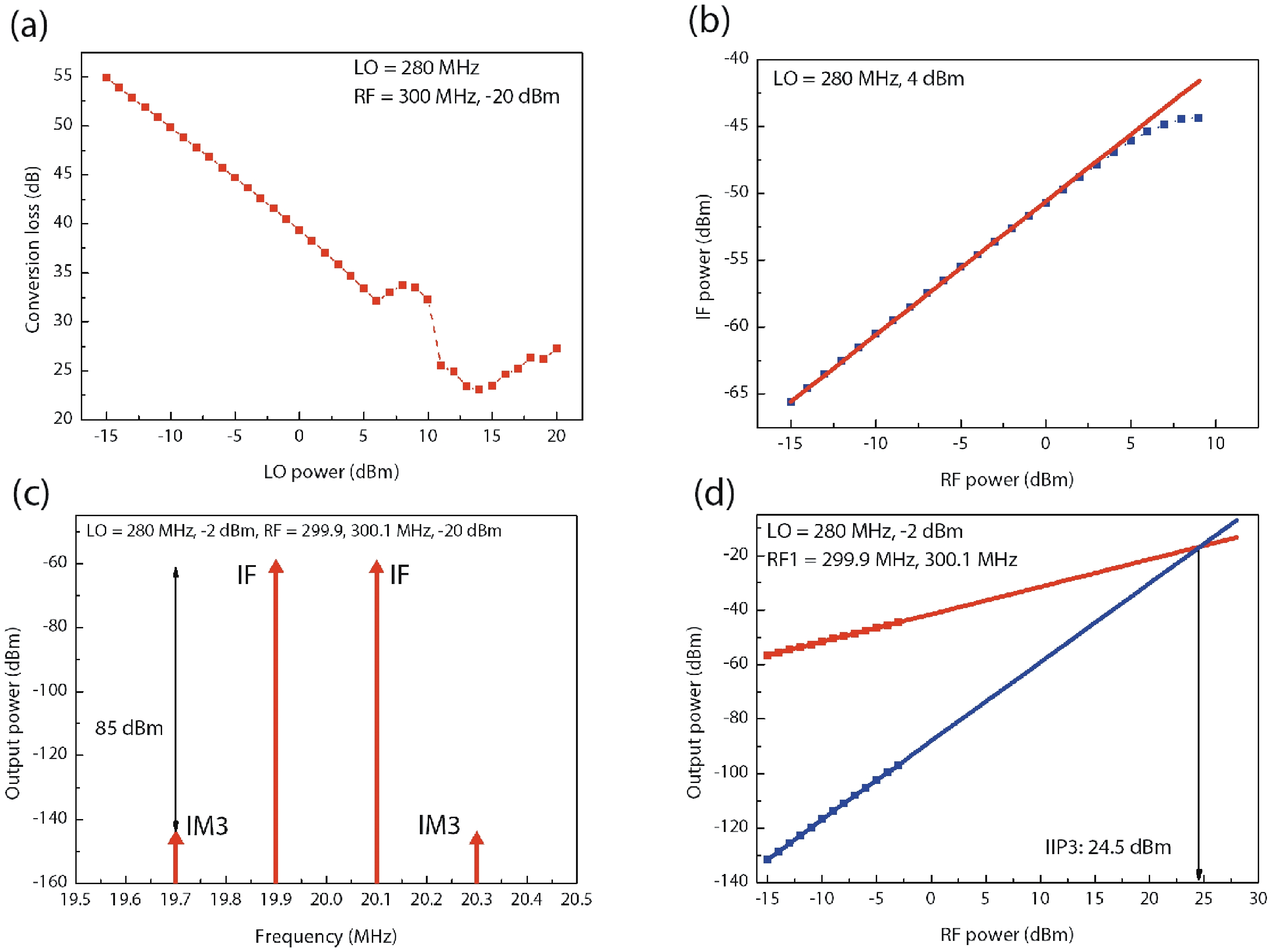
Graphene field-effect transistors (GFET) have attracted much attention in the radio frequency (RF) and microwave fields because of its extremely high carrier mobility. In this paper, a GFET with a gate length of 5 μm is fabricated through the van der Walls (vdW) transfer process, and then the existing large-signal GFET model is described, and the model is implemented in Verilog-A for analysis in RF and microwave circuits. Next a double-balanced mixer based on four GFETs is designed and analyzed in advanced design system (ADS) tools. Finally, the simulation results show that with the input of 300 and 280 MHz, the IIP3 of the mixed signal is 24.5 dBm.

J. Semicond.
2022, 43(5): 052003 doi: 10.1088/1674-4926/43/5/052003

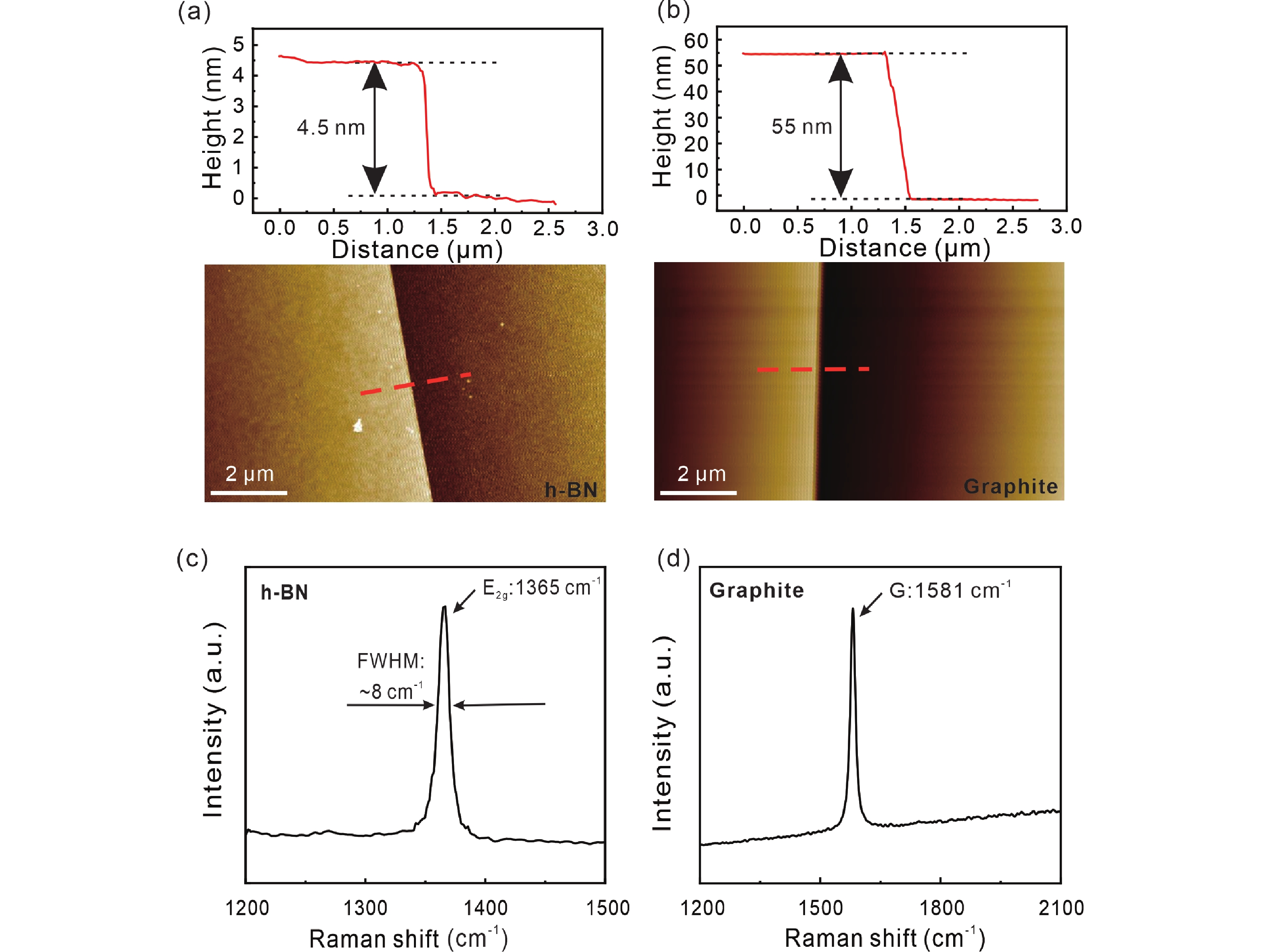
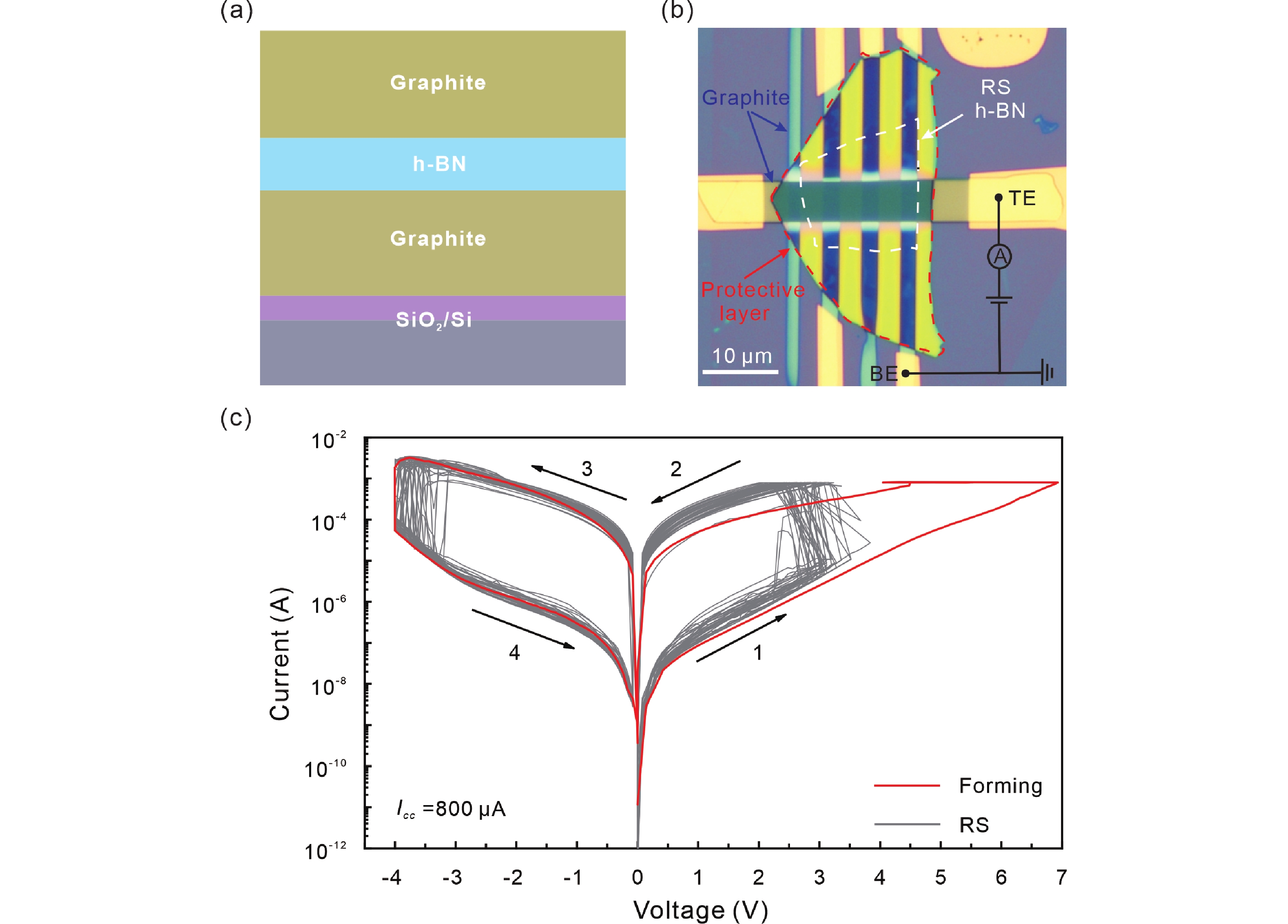
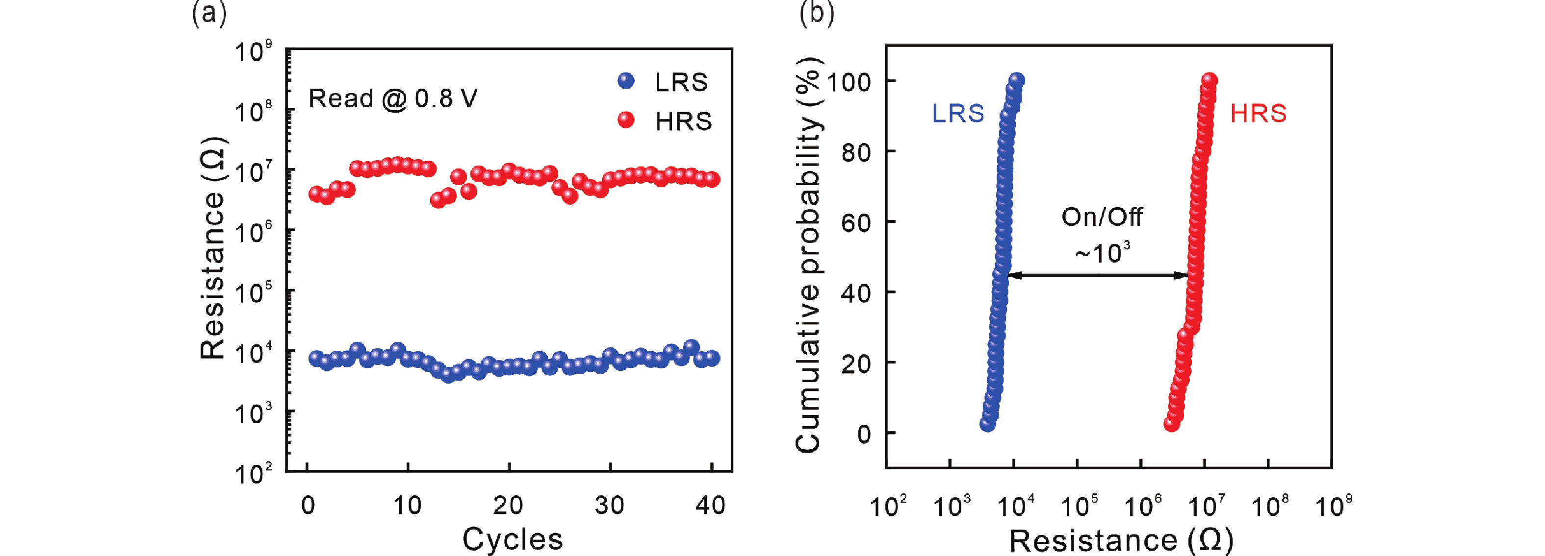
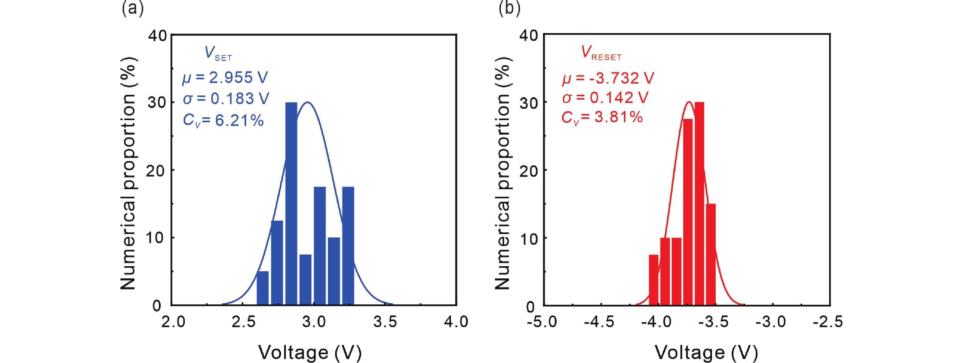
With the atomically sharp interface and stable switching channel, van der Waals (vdW) heterostructure memristors have attracted extensive interests for the application of high-density memory and neuromorphic computing. Here, we demonstrate a new type of vdW heterostructure memristor device by sandwiching a single-crystalline h-BN layer between two thin graphites. In such a device, a stable bipolar resistive switching (RS) behavior has been observed for the first time. We also characterize their switching performance, and observe an on/off ratio of >103 and a minimum RESET voltage variation coefficient of 3.81%. Our work underscores the potential of 2D materials and vdW heterostructures for emerging memory and neuromorphic applications.
J. Semicond.
2022, 43(5): 054101 doi: 10.1088/1674-4926/43/5/054101
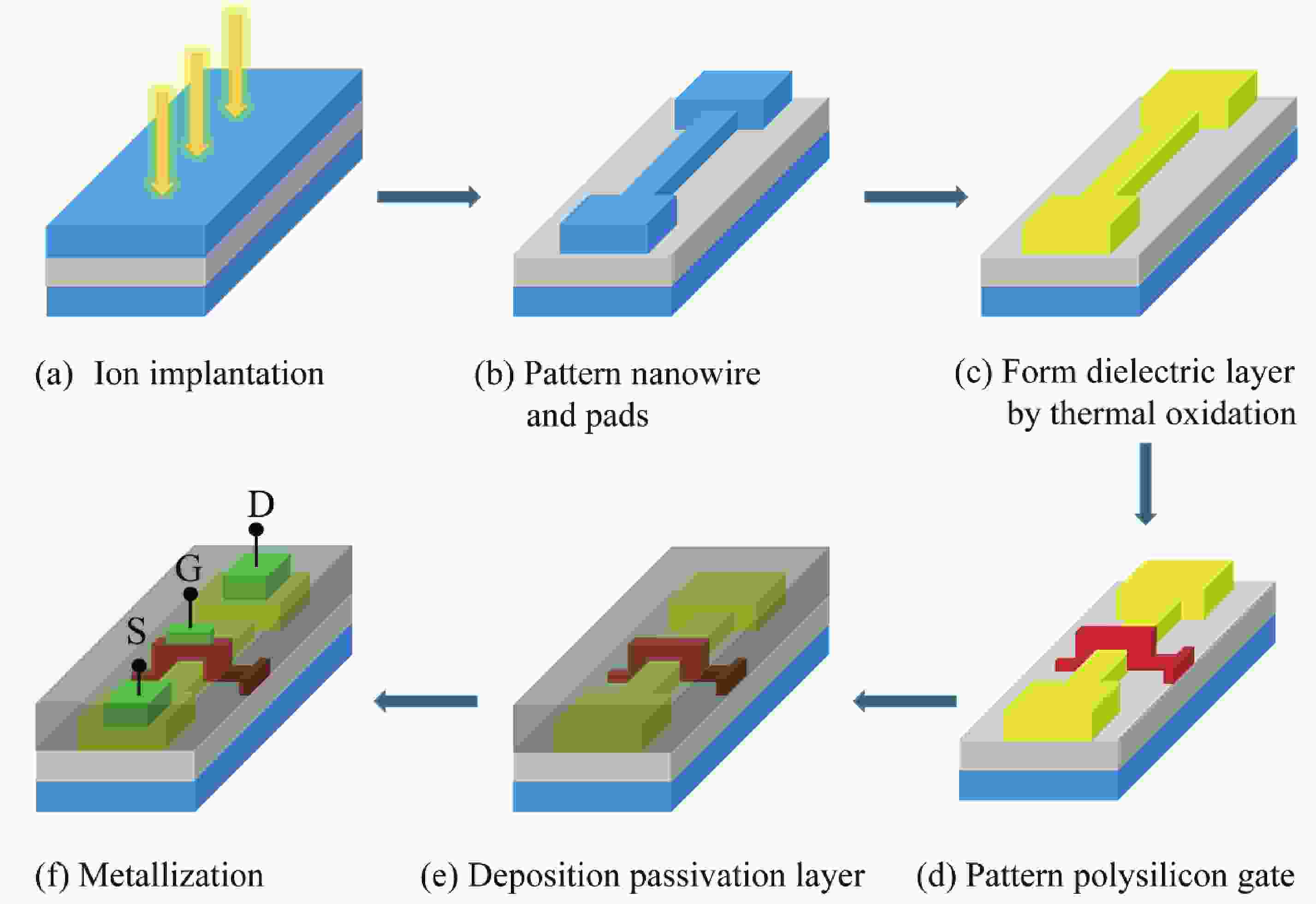
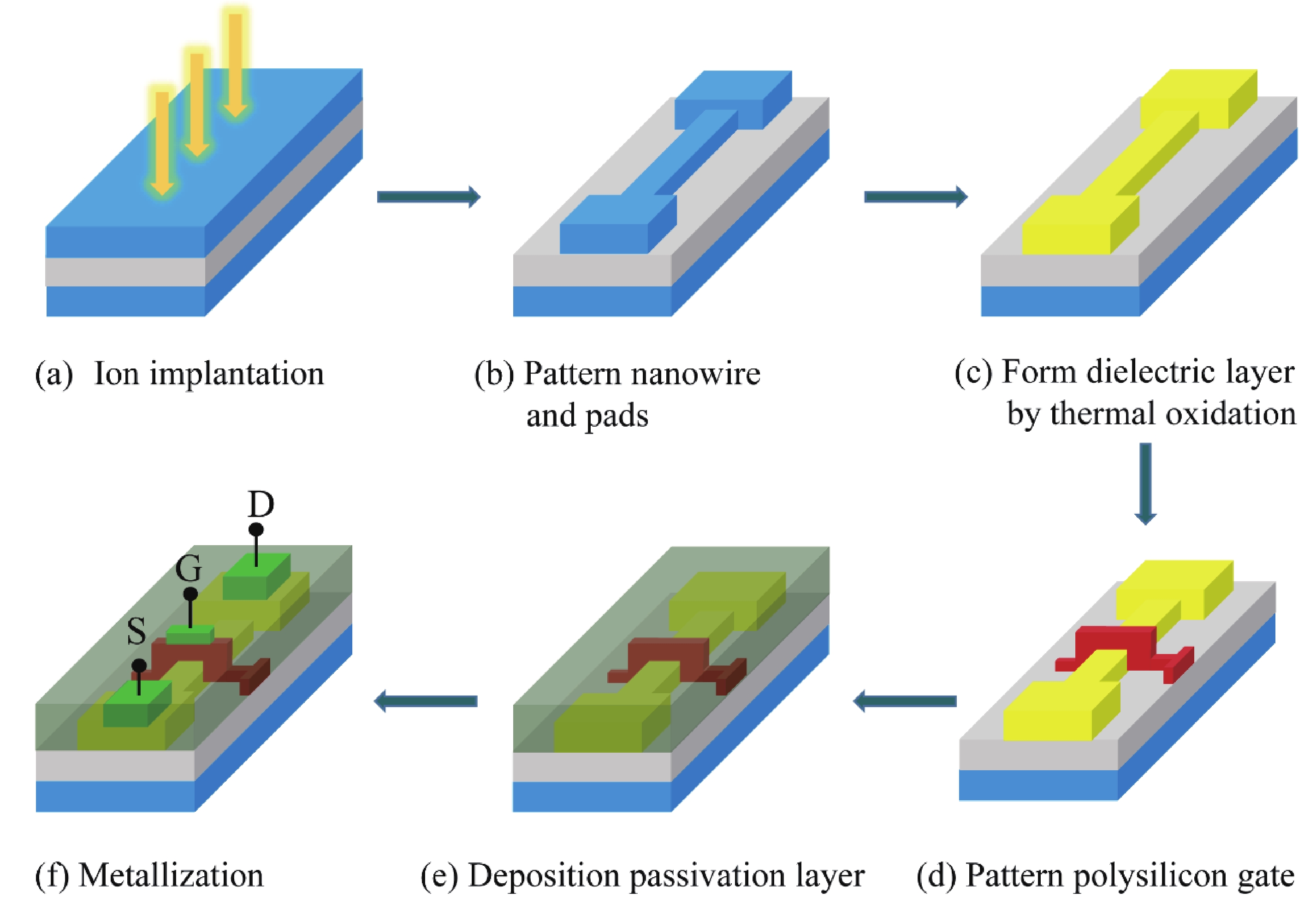
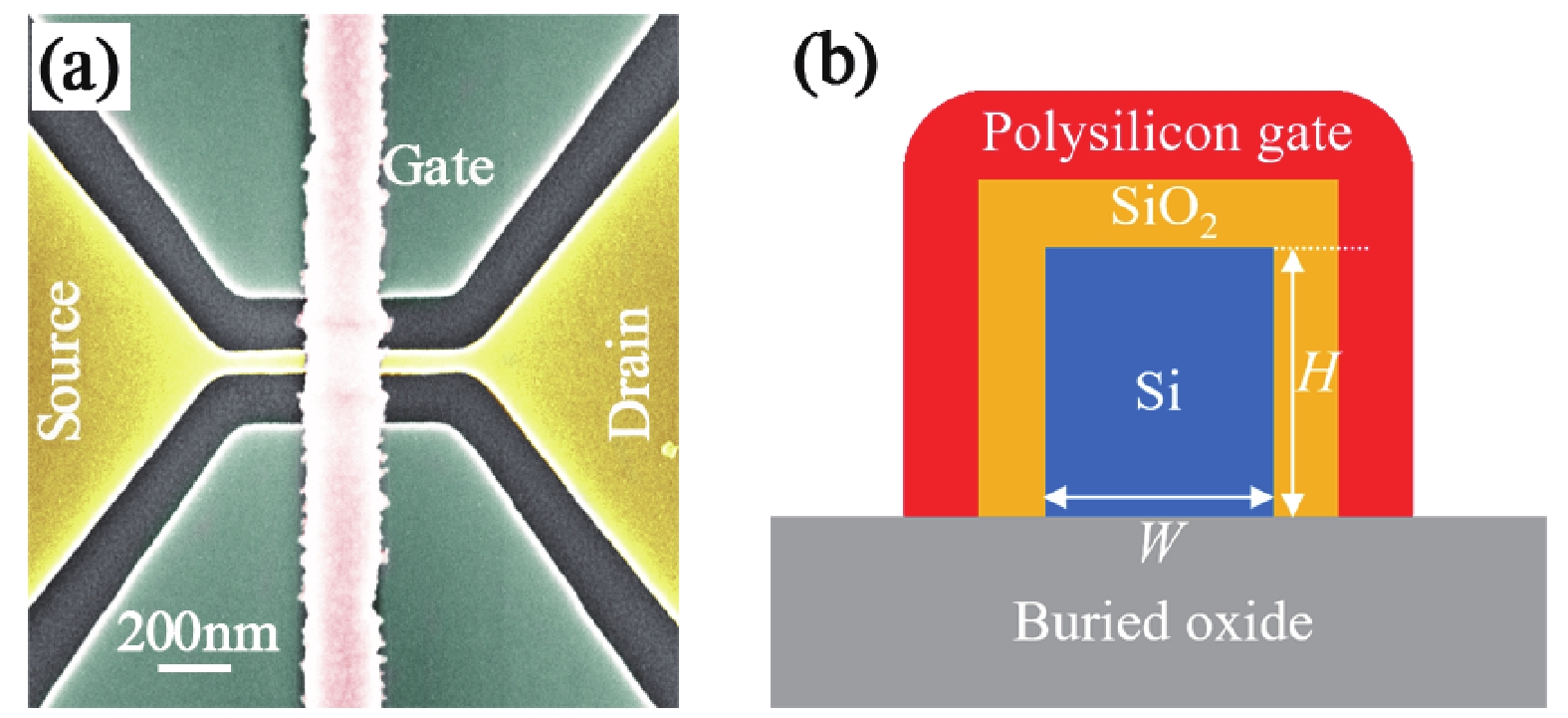
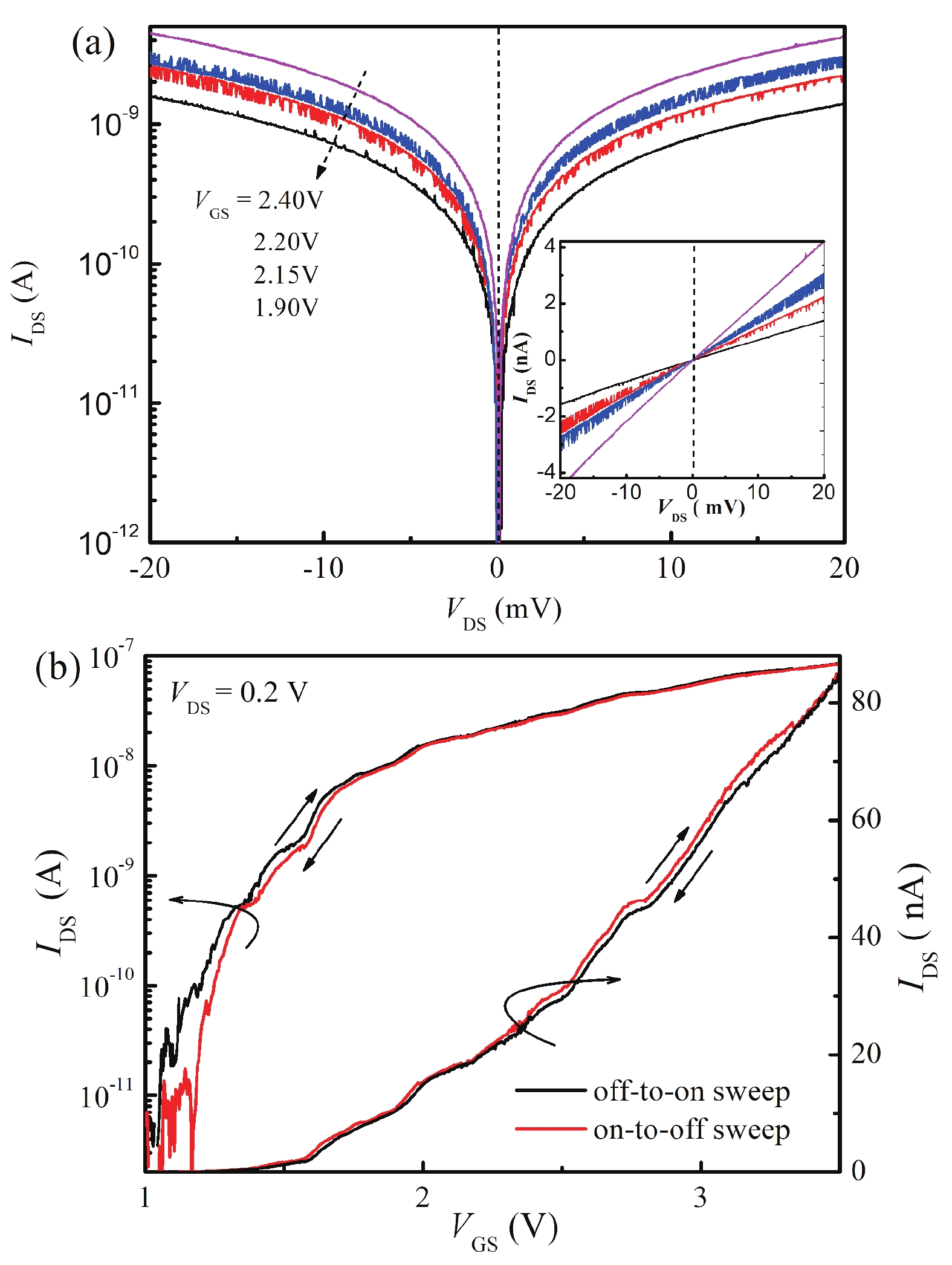
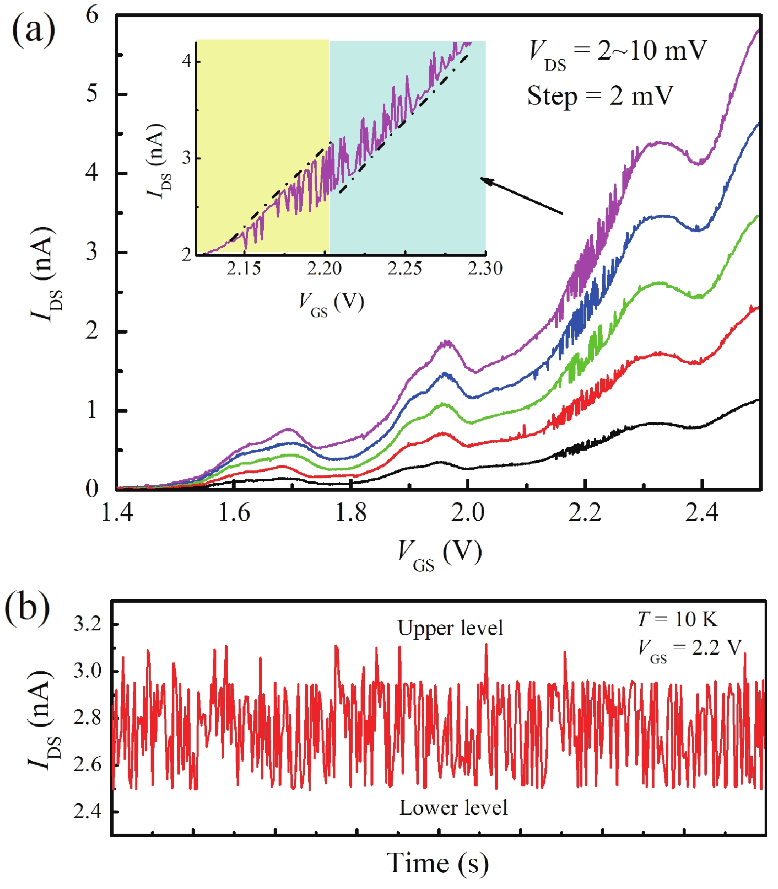
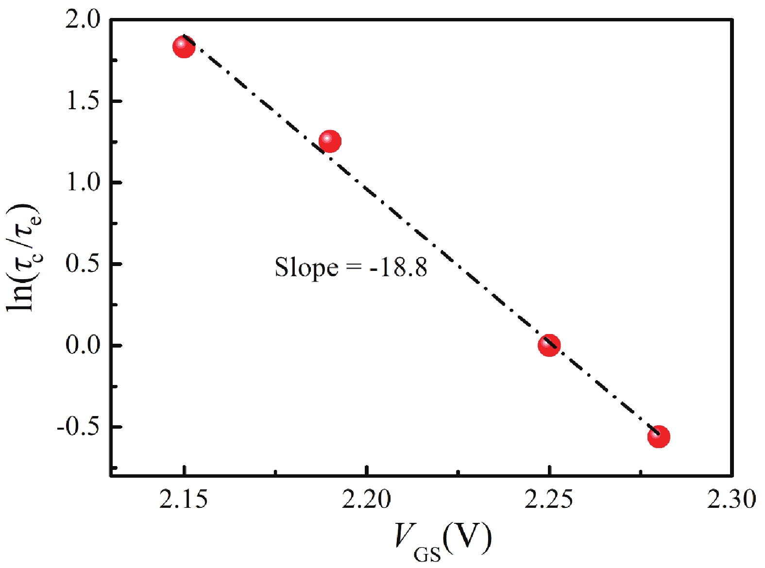
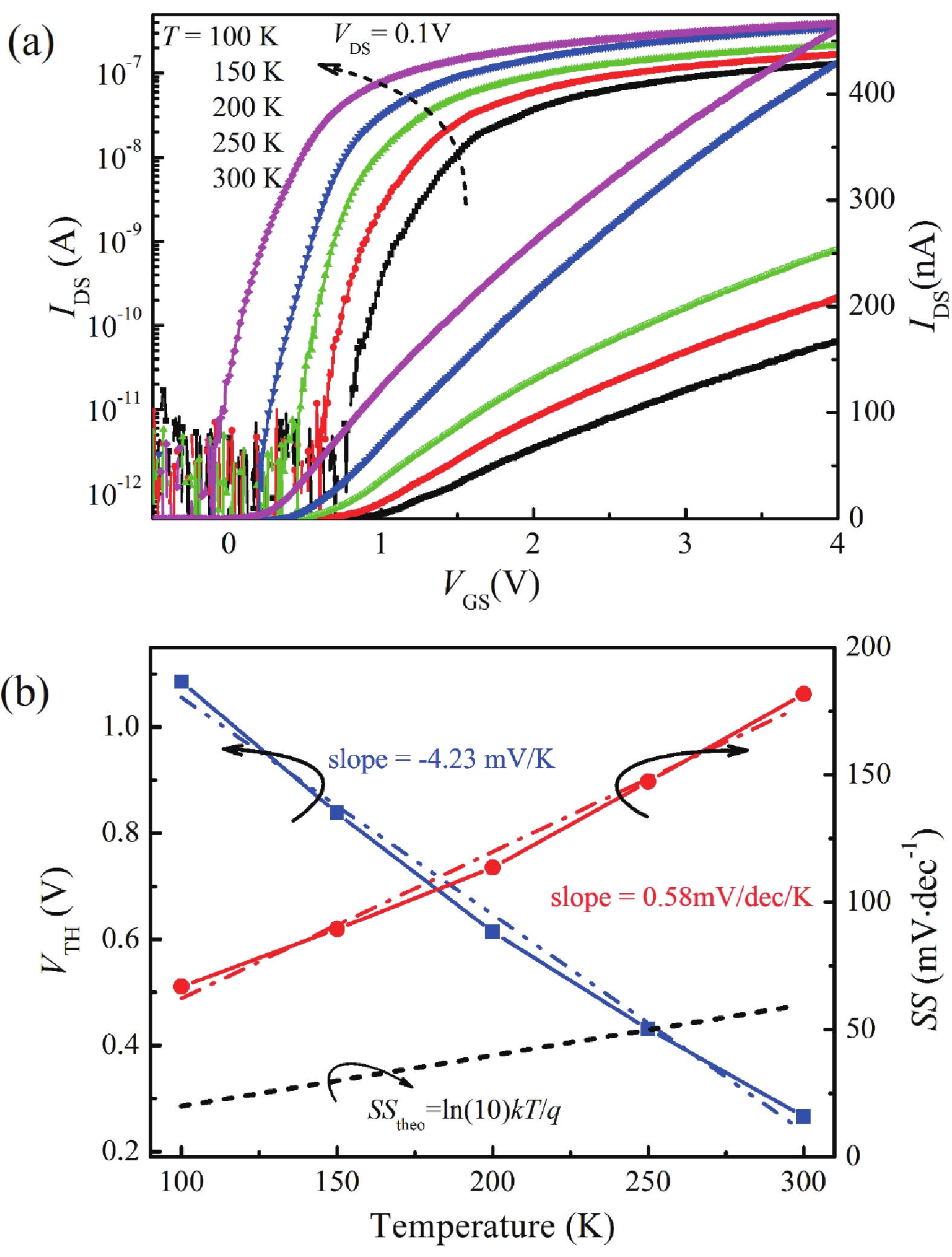
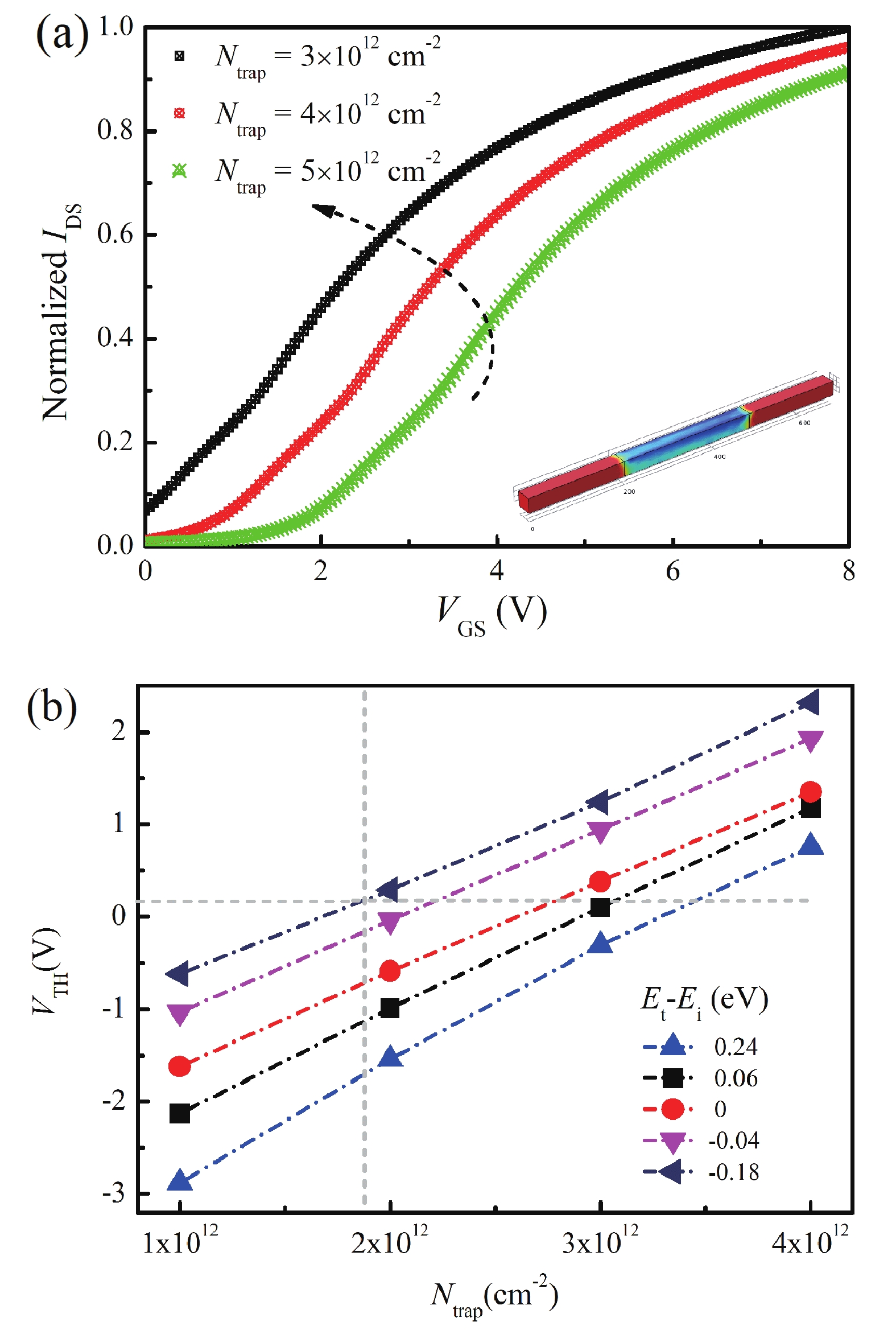
We investigated the effect of charge trapping on electrical characteristics of silicon junctionless nanowire transistors which are fabricated on heavily n-type doped silicon-on-insulator substrate. The obvious random telegraph noise and current hysteresis observed at the temperature of 10 K indicate the existence of acceptor-like traps. The position depth of the traps in the oxide from Si/SiO2 interface is 0.35 nm, calculated by utilizing the dependence of the capture and emission time on the gate voltage. Moreover, by constructing a three-dimensional model of tri-gate device structure in COMSOL Multiphysics simulation software, we achieved the trap density of 1.9 × 1012 cm–2 and the energy level position of traps at 0.18 eV below the intrinsic Fermi level.

J. Semicond.
2022, 43(5): 054102 doi: 10.1088/1674-4926/43/5/054102

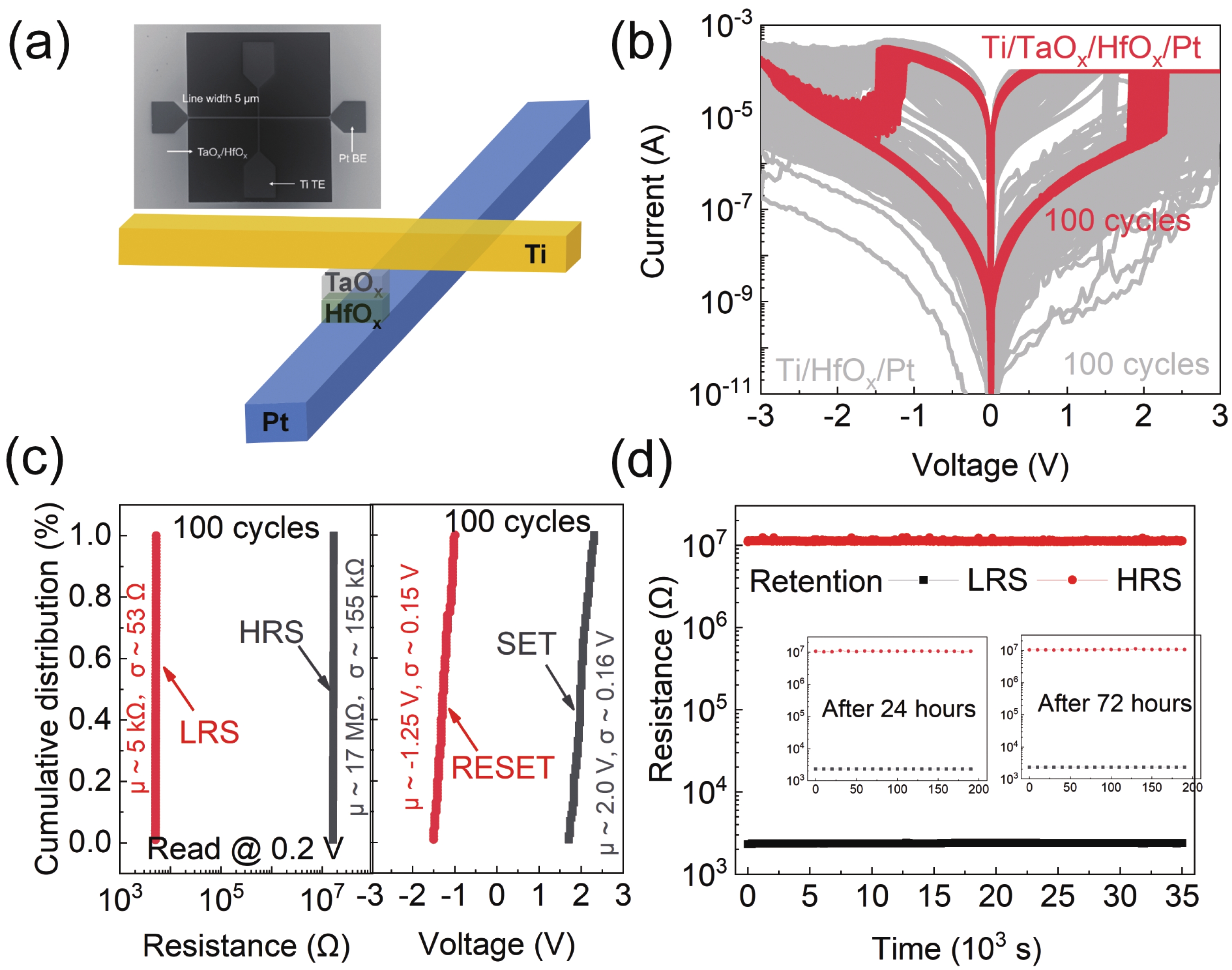
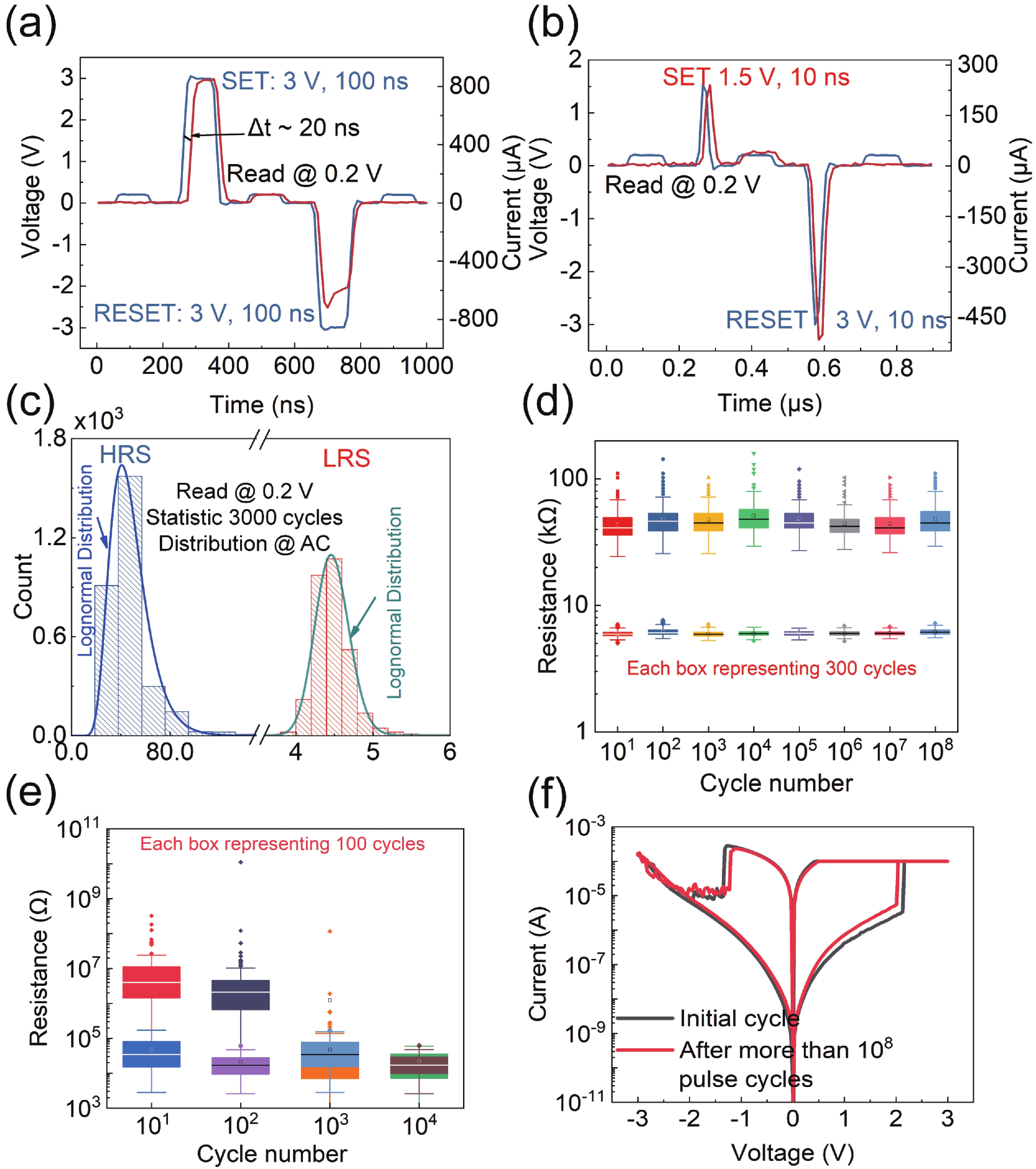
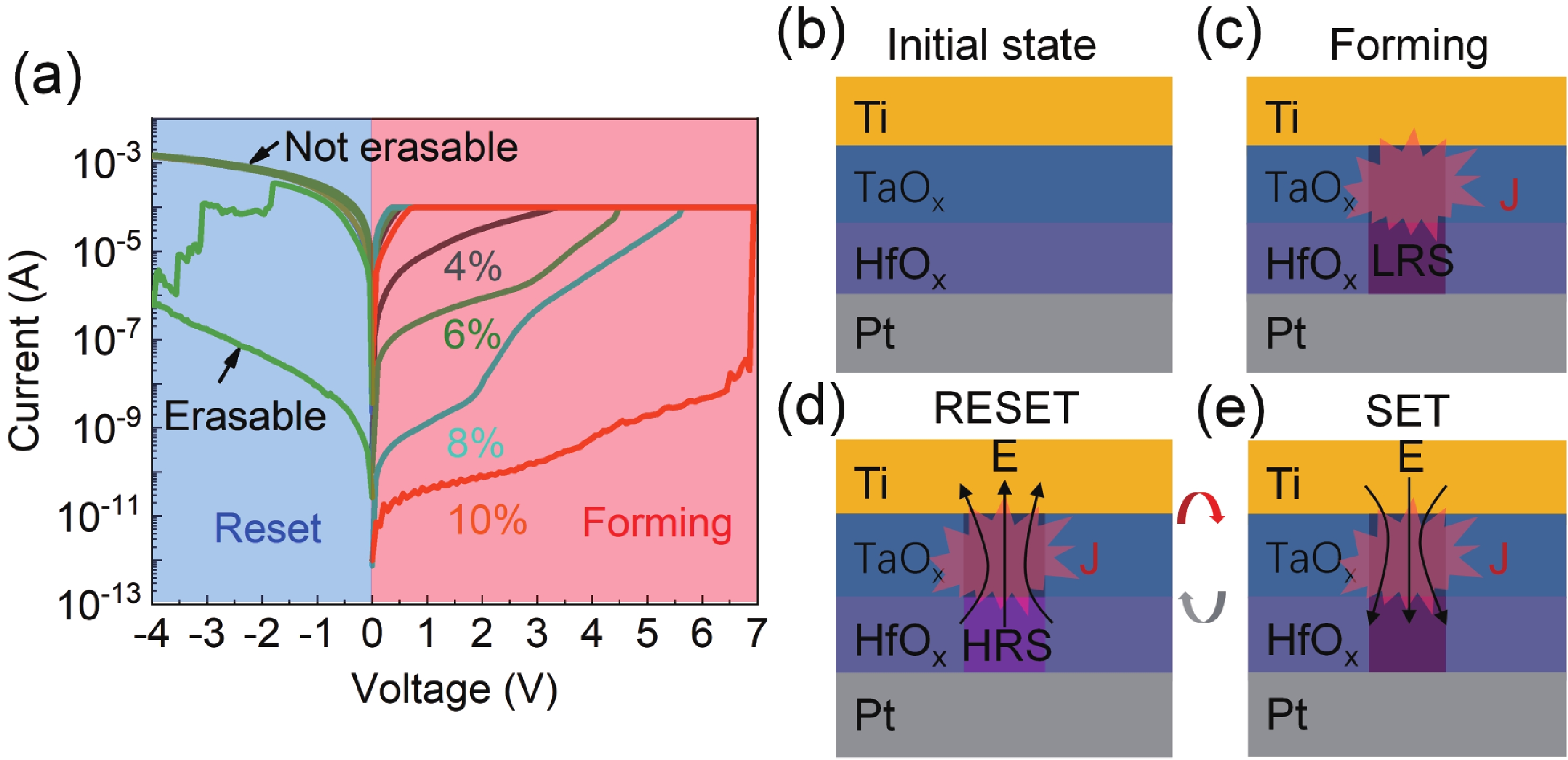
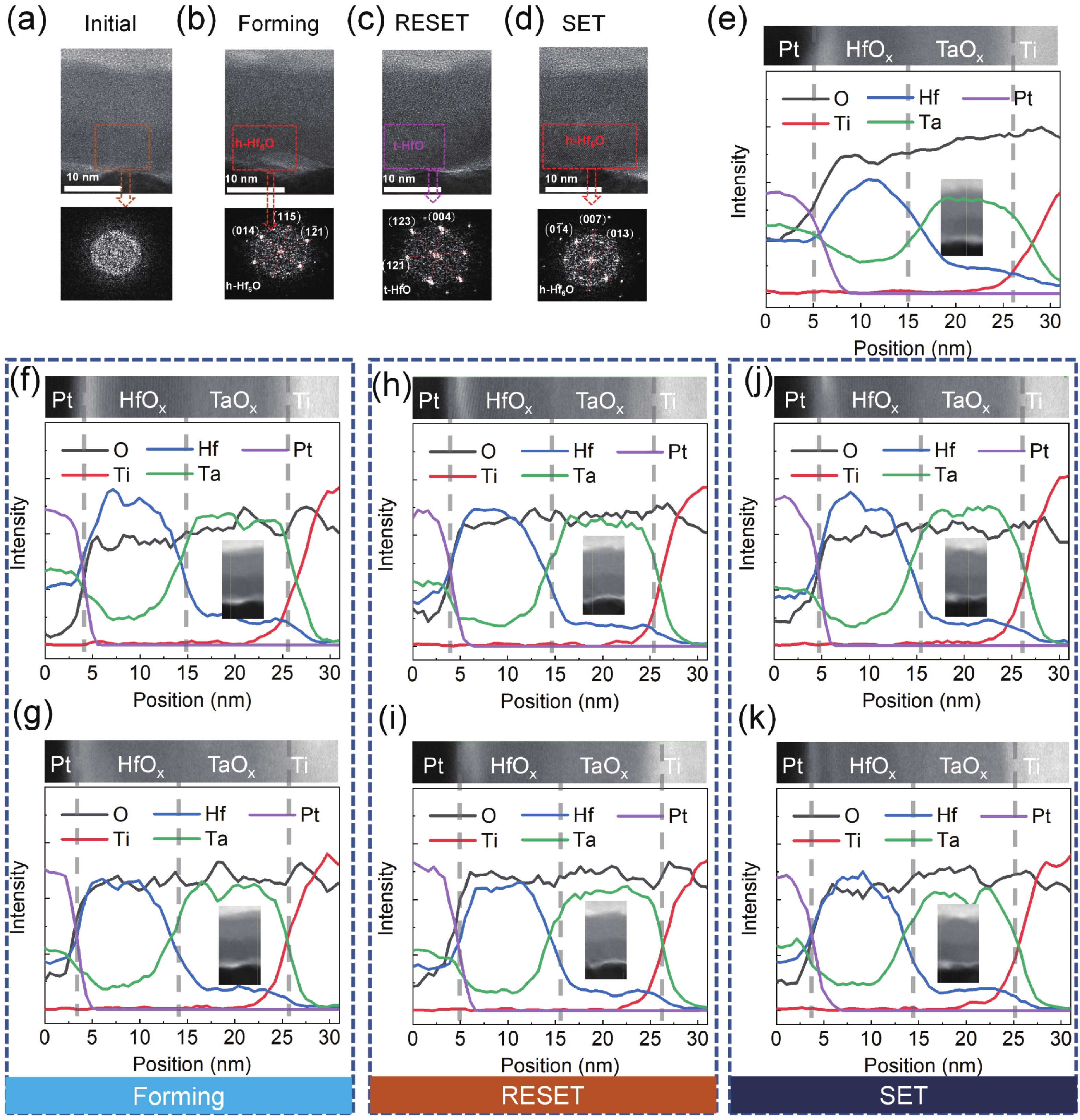
Resistive switching random access memory (RRAM) is considered as one of the potential candidates for next-generation memory. However, obtaining an RRAM device with comprehensively excellent performance, such as high retention and endurance, low variations, as well as CMOS compatibility, etc., is still an open question. In this work, we introduce an insert TaOx layer into HfOx-based RRAM to optimize the device performance. Attributing to robust filament formed in the TaOx layer by a forming operation, the local-field and thermal enhanced effect and interface modulation has been implemented simultaneously. Consequently, the RRAM device features large windows (> 103), fast switching speed (~ 10 ns), steady retention (> 72 h), high endurance (> 108 cycles), and excellent uniformity of both cycle-to-cycle and device-to-device. These results indicate that inserting the TaOx layer can significantly improve HfOx-based device performance, providing a constructive approach for the practical application of RRAM.
J. Semicond.
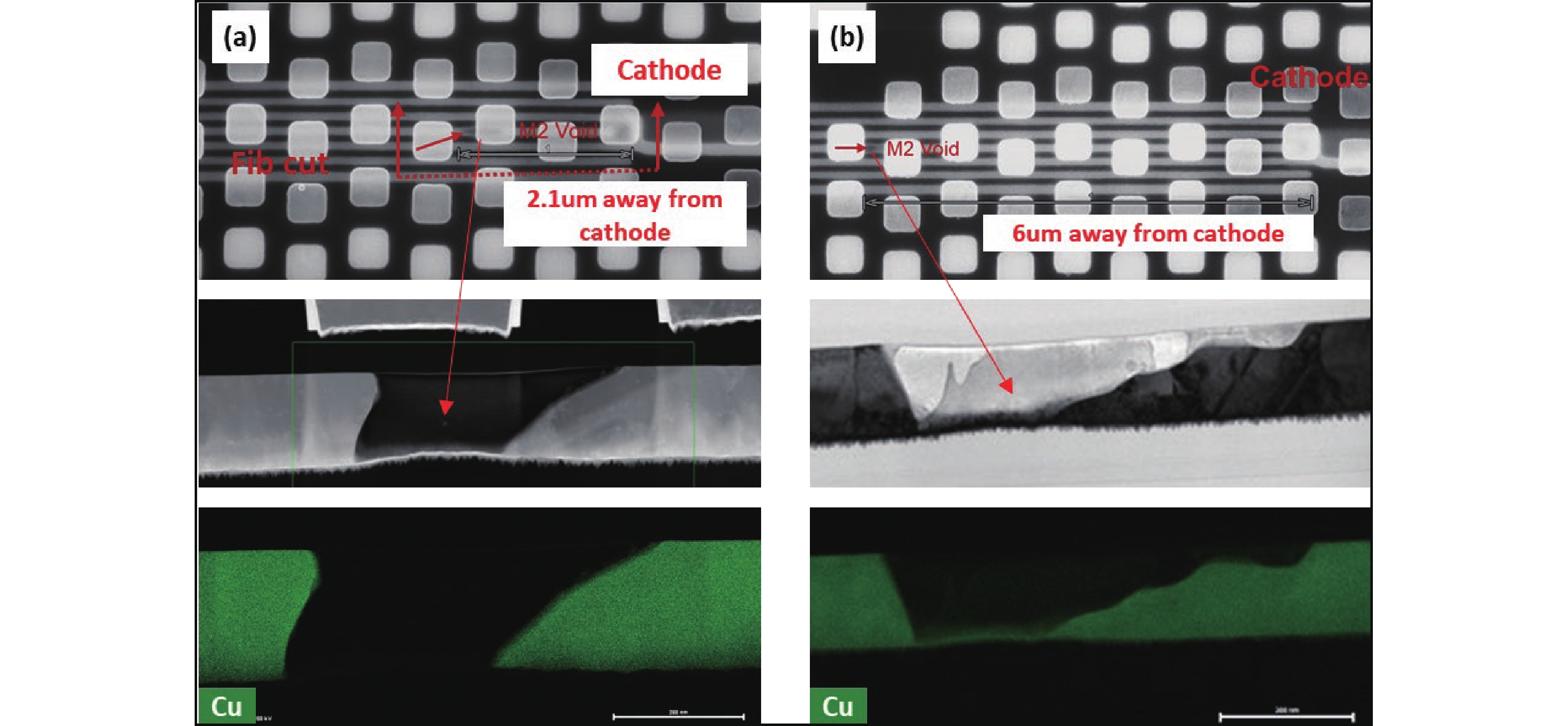
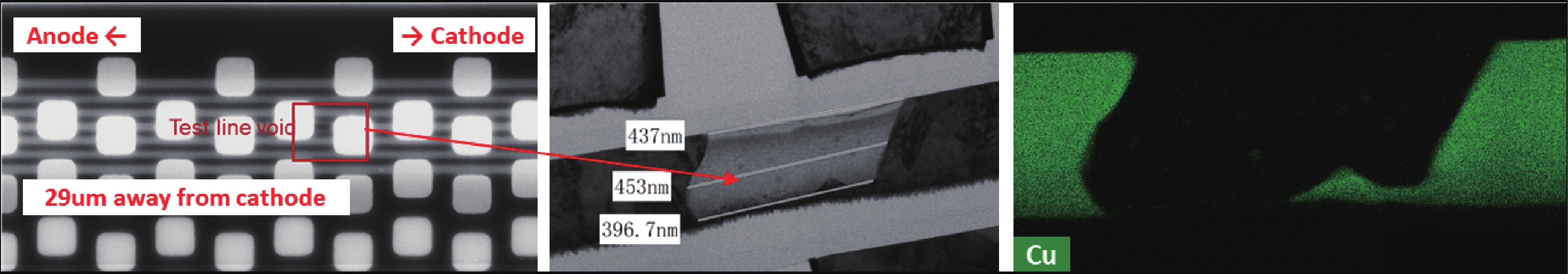
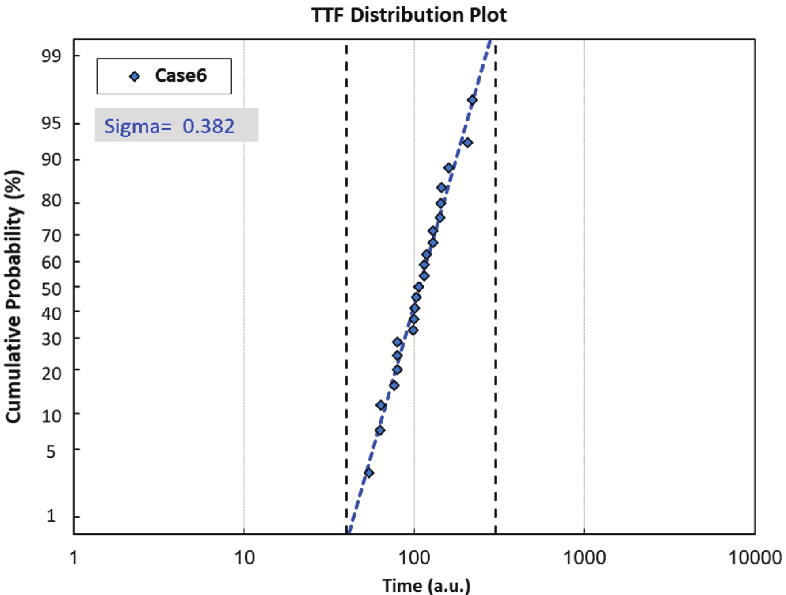
2022, 43(5): 054103 doi: 10.1088/1674-4926/43/5/054103
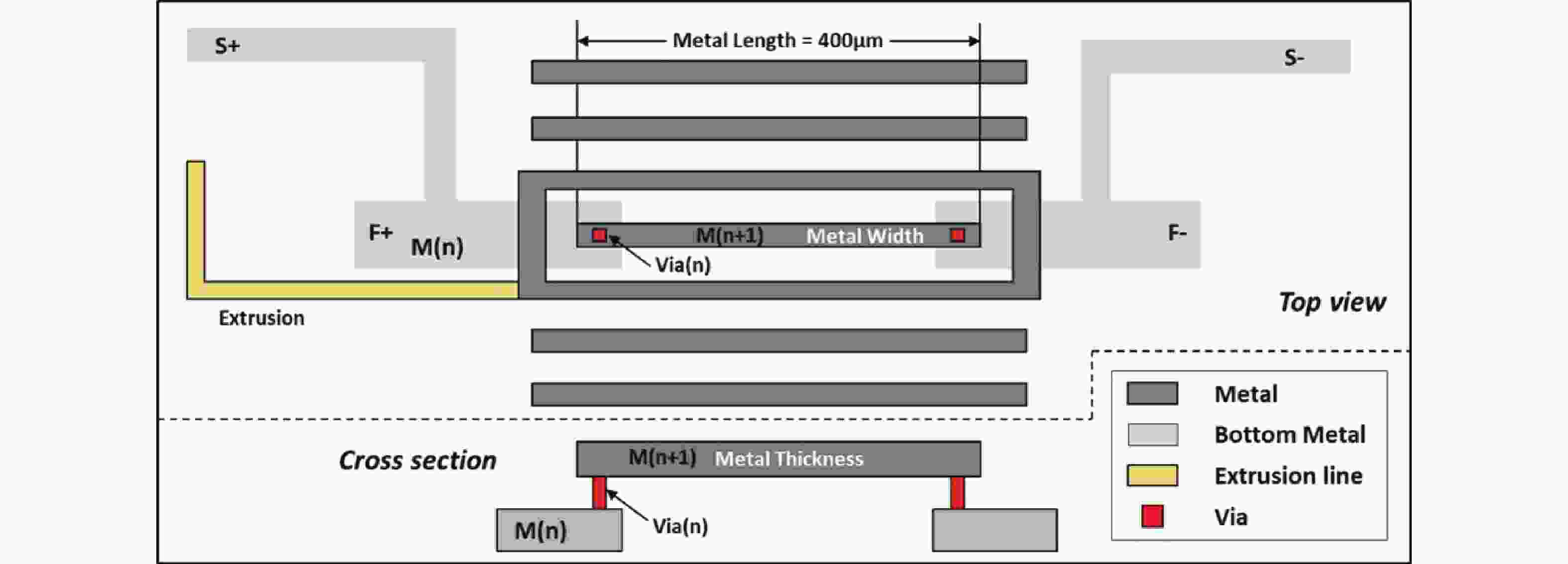
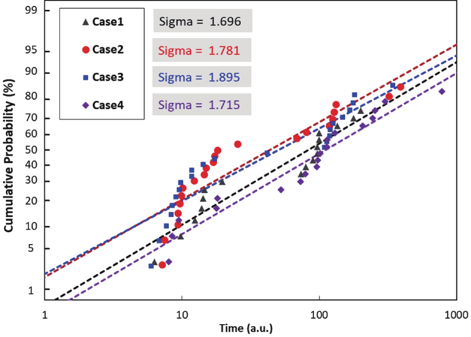
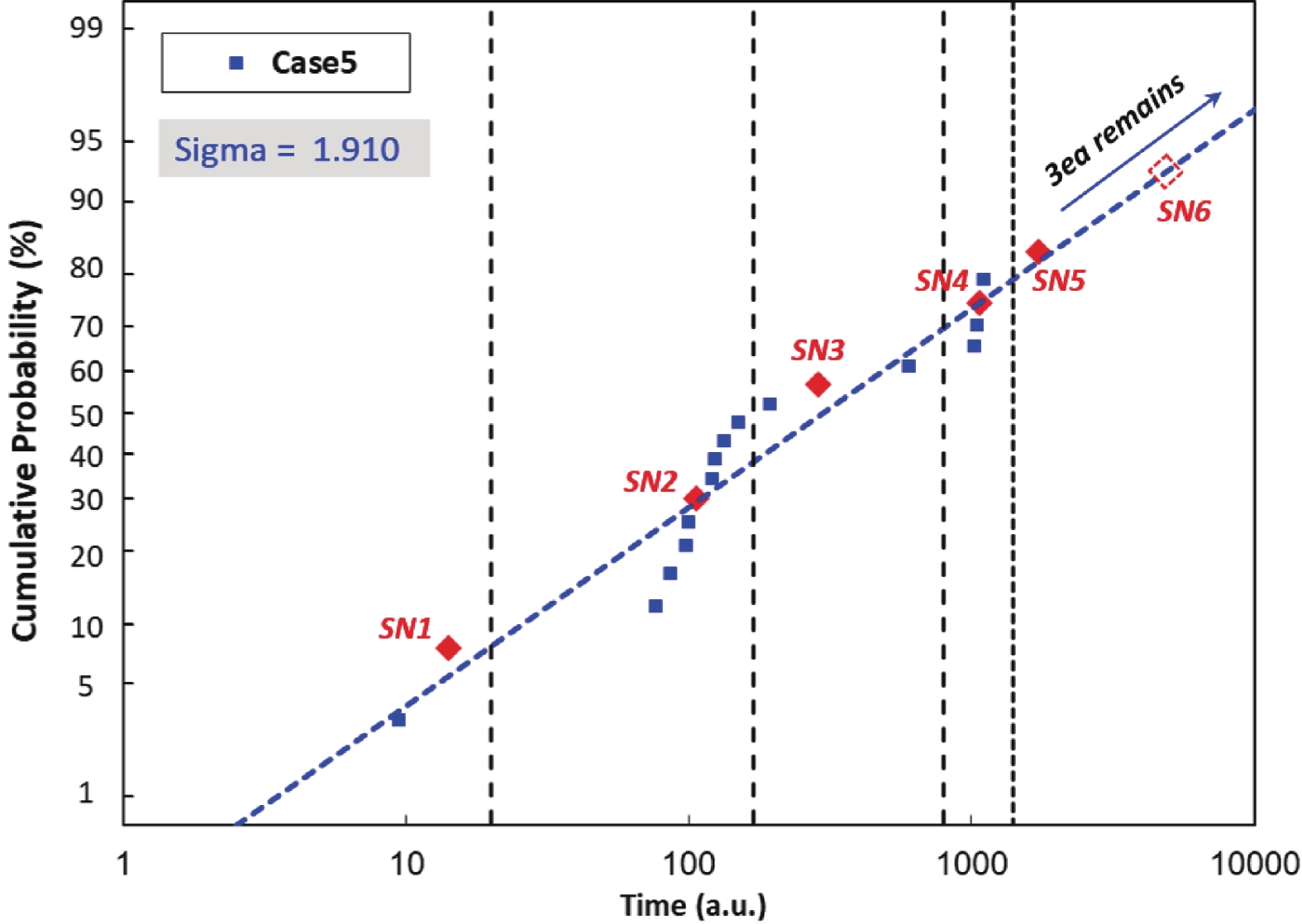
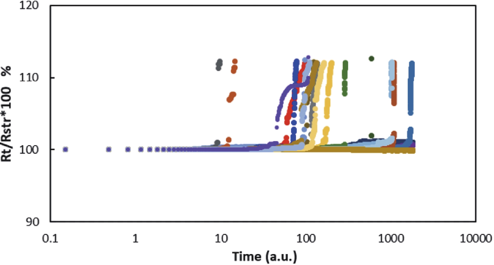
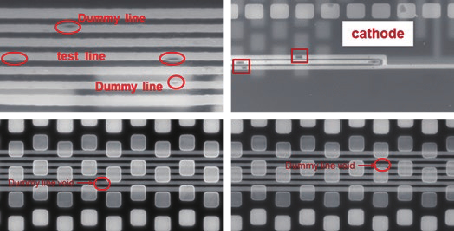
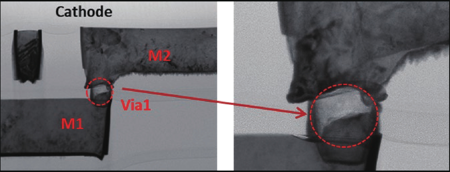
A multi-modal time-to-failure distribution for an electro-migration (EM) structure has been observed and studied from long duration in-situ EM experiment, for which the failure mechanism has been investigated and discussed comprehensively. The mixed EM failure behavior strongly suggest that the fatal voids induced EM failure appear at various locations along the EM structure. This phenomenon is believed to be highly related to the existence of pre-existing voids before EM stress. Meanwhile, the number and location of the pre-existing voids can influence the EM failure mode significantly. Based on our research, a potential direction to improve the EM lifetime of Cu interconnect is presented.


J. Semicond.
2022, 43(5): 052001 doi: 10.1088/1674-4926/43/5/052001
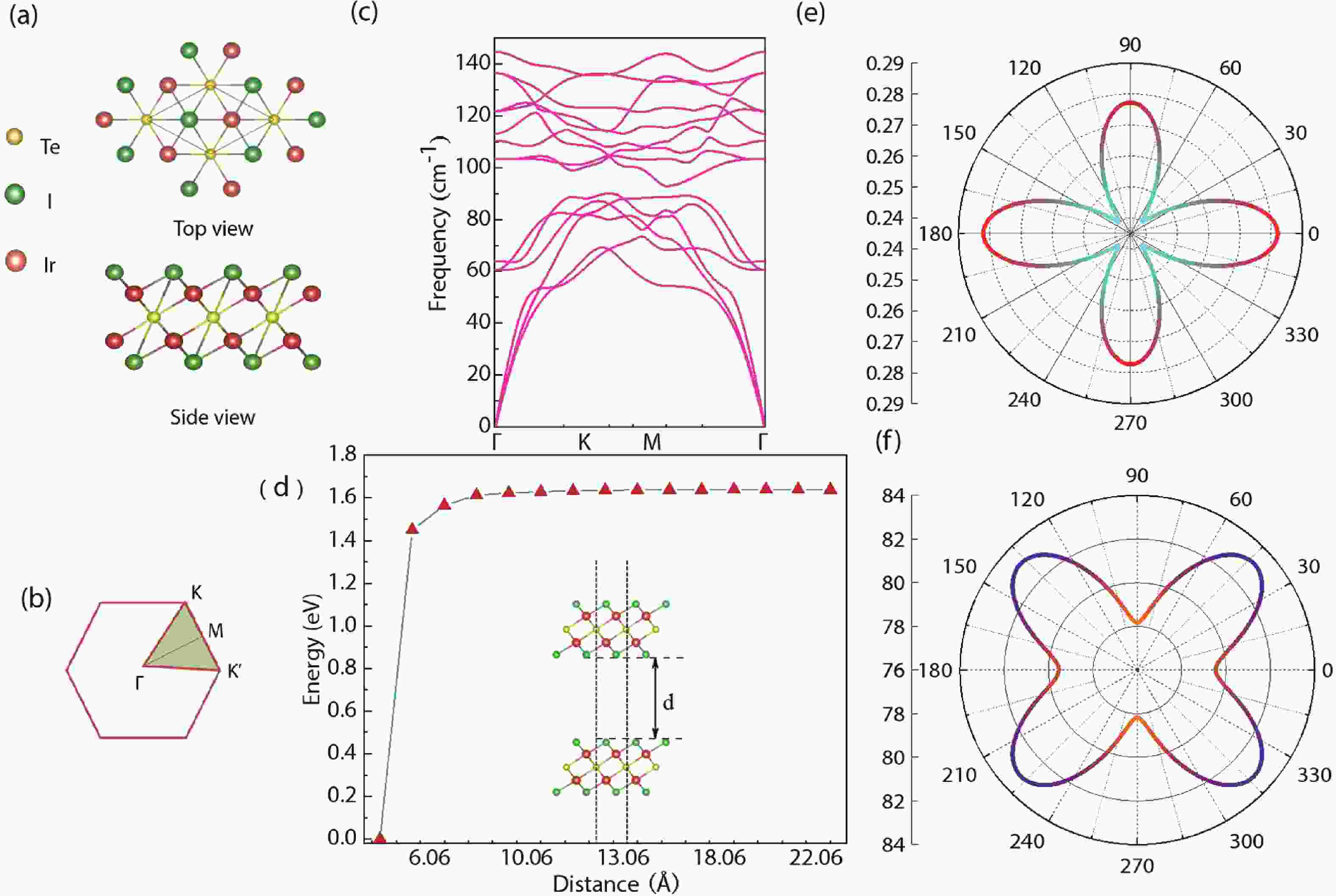
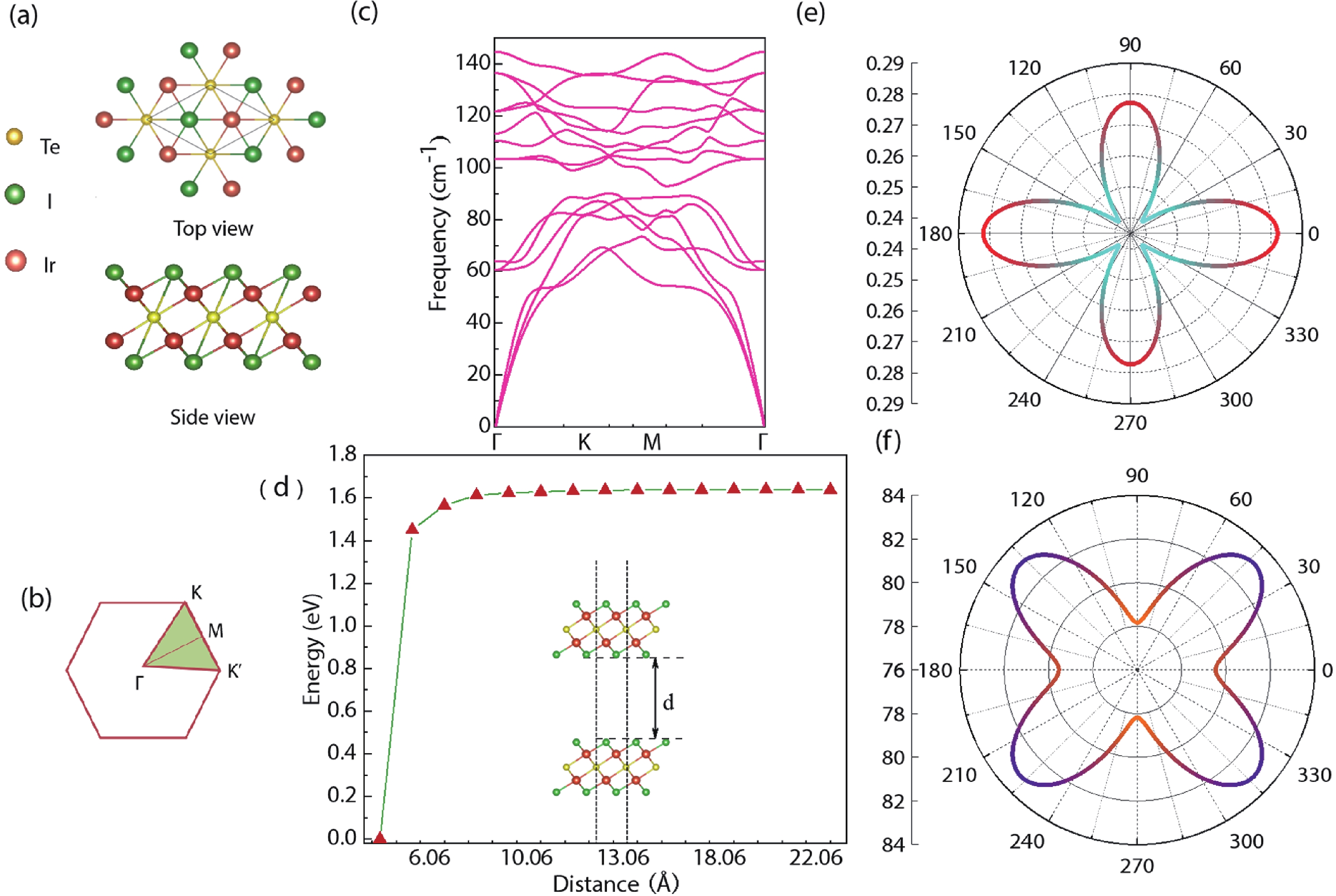
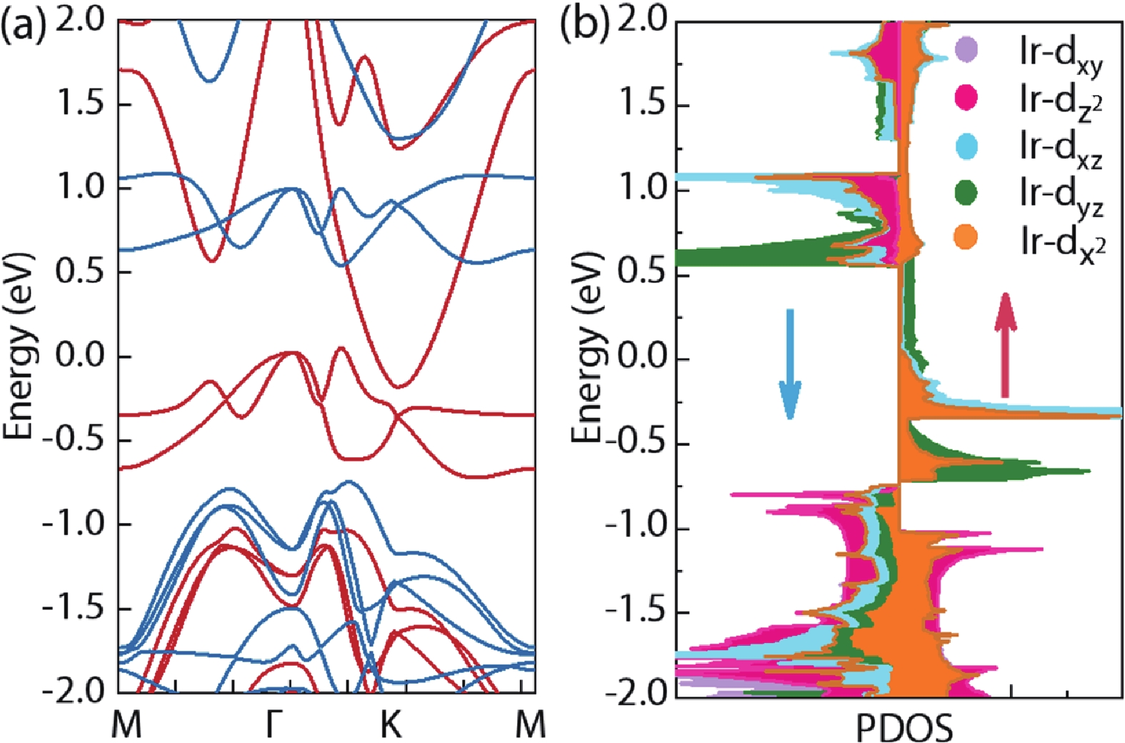
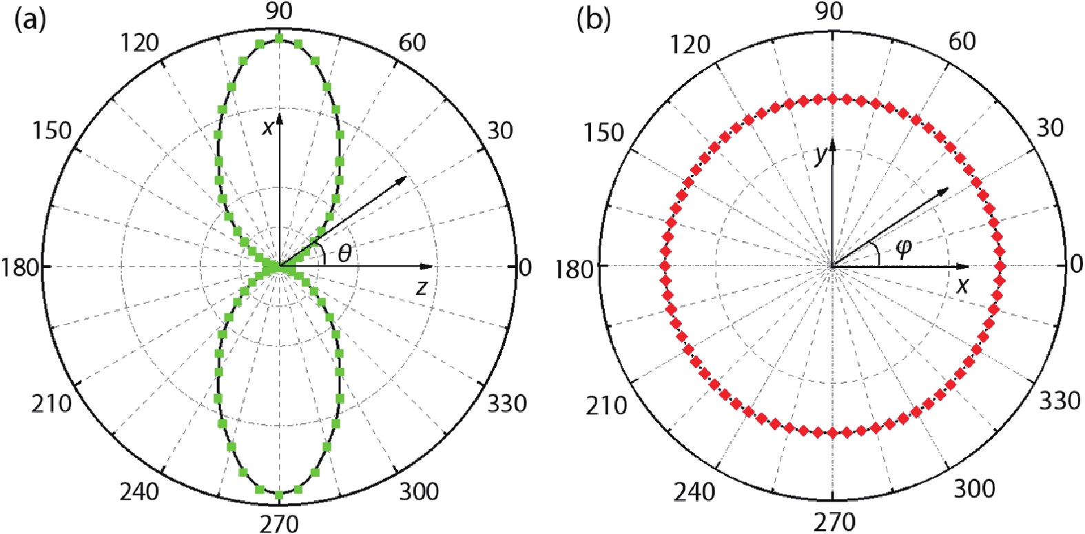
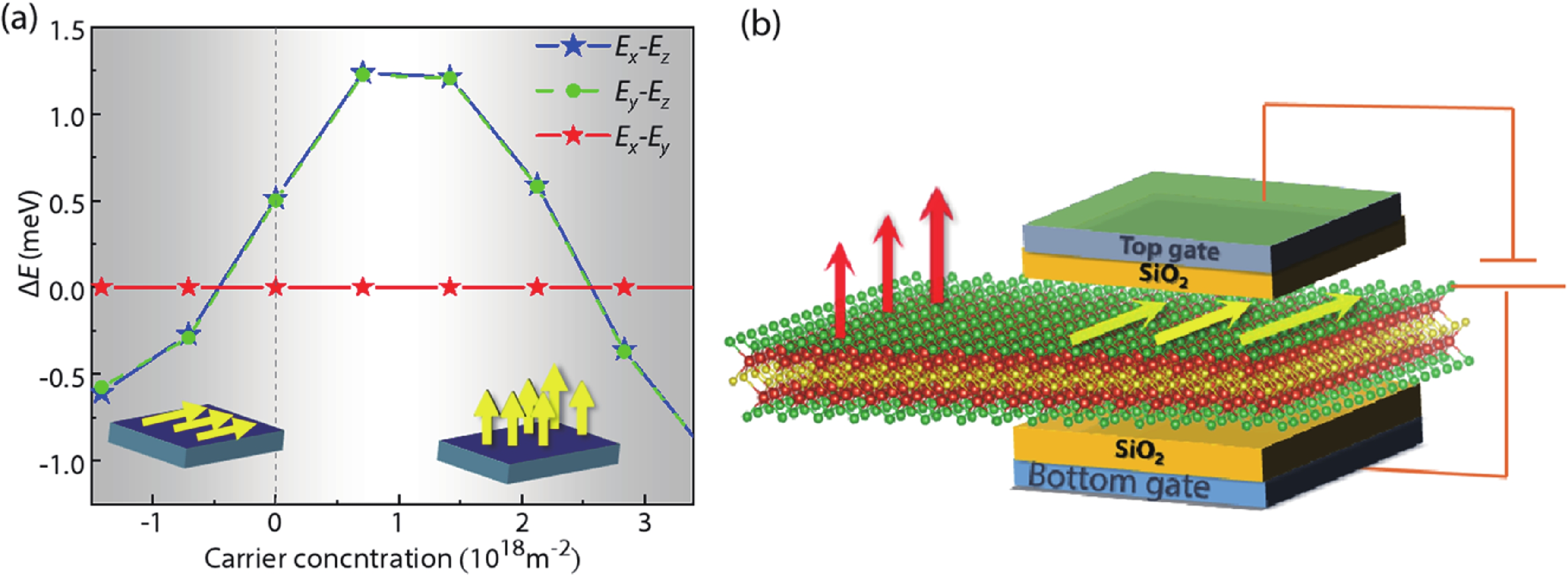
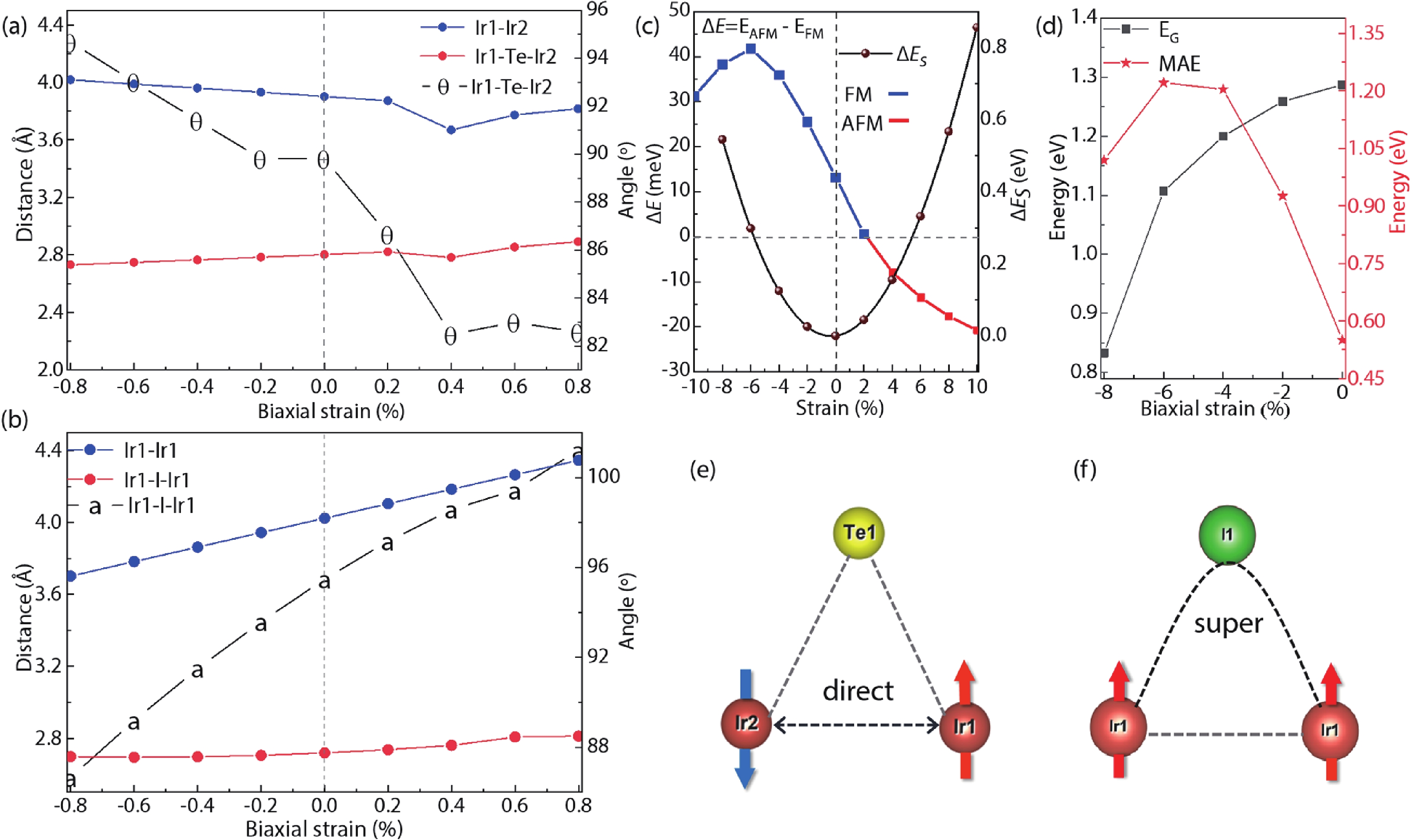
A two-dimensional (2D) high-temperature ferromagnetic half-metal whose magnetic and electronic properties can be flexibly tuned is required for the application of new spintronics devices. In this paper, we predict a stable Ir2TeI2 monolayer with half-metallicity by systematical first-principles calculations. Its ground state is found to exhibit inherent ferromagnetism and strong out-of-plane magnetic anisotropy of up to 1.024 meV per unit cell. The Curie temperature is estimated to be 293 K based on Monte Carlo simulation. Interestingly, a switch of magnetic axis between in-plane and out-of-plane is achievable under hole and electron doping, which allows for the effective control of spin injection/detection in such 2D systems. Furthermore, the employment of biaxial strain can realize the transition between ferromagnetic and antiferromagnetic states. These findings not only broaden the scope of 2D half-metal materials but they also provide an ideal platform for future applications of multifunctional spintronic devices.

J. Semicond.
2022, 43(5): 052201 doi: 10.1088/1674-4926/43/5/052201

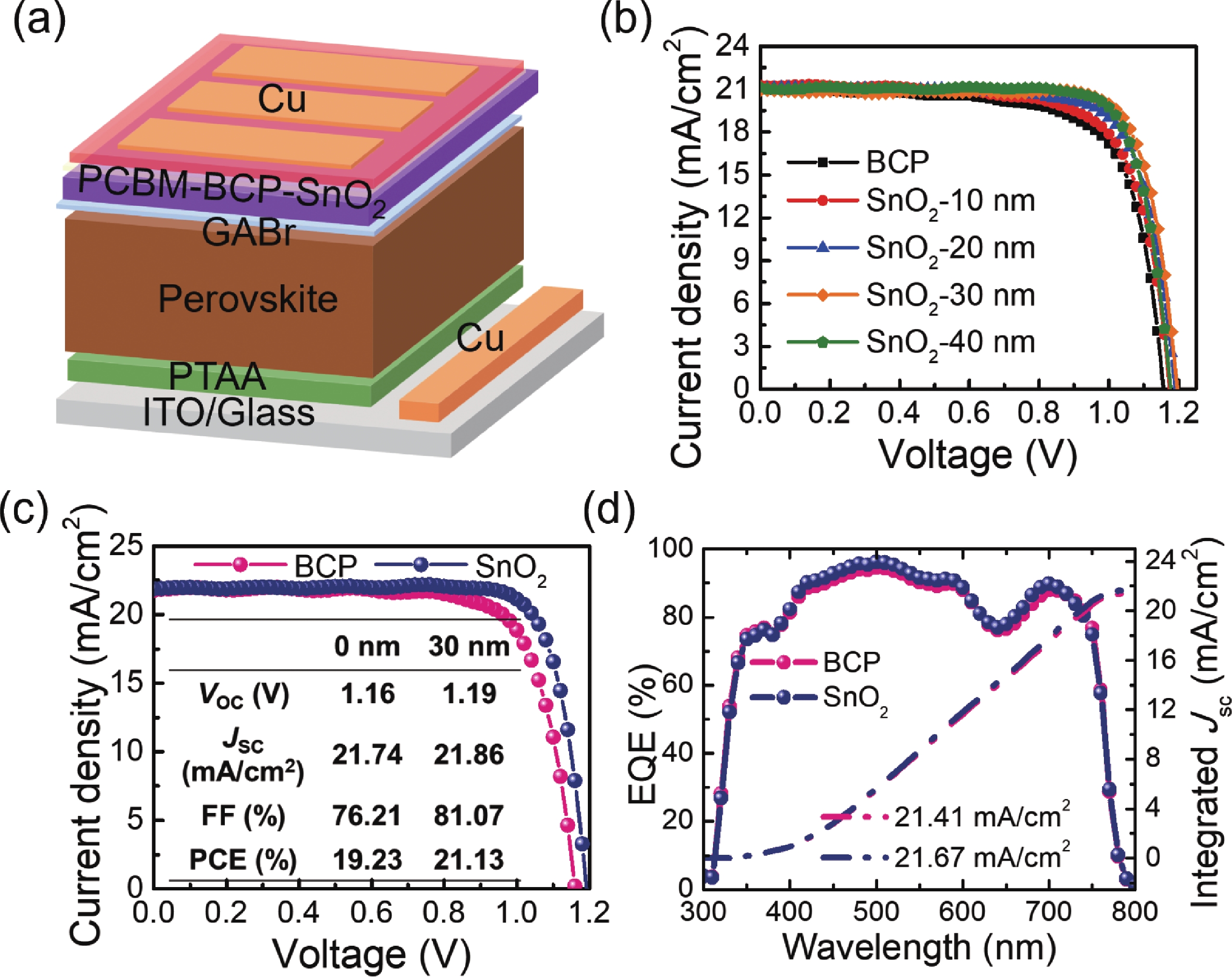
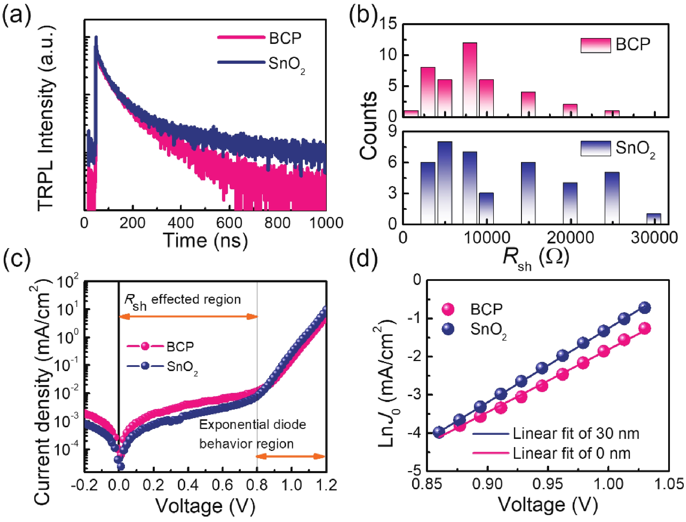
Inverted perovskite solar cells (IPSCs) have attracted tremendous research interest in recent years due to their applications in perovskite/silicon tandem solar cells. However, further performance improvements and long-term stability issues are the main obstacles that deeply hinder the development of devices. Herein, we demonstrate a facile atomic layer deposition (ALD) processed tin dioxide (SnO2) as an additional buffer layer for efficient and stable wide-bandgap IPSCs. The additional buffer layer increases the shunt resistance and reduces the reverse current saturation density, resulting in the enhancement of efficiency from 19.23% to 21.13%. The target device with a bandgap of 1.63 eV obtains open-circuit voltage of 1.19 V, short circuit current density of 21.86 mA/cm2, and fill factor of 81.07%. More importantly, the compact and stable SnO2 film invests the IPSCs with superhydrophobicity, thus significantly enhancing the moisture resistance. Eventually, the target device can maintain 90% of its initial efficiency after 600 h storage in ambient conditions with relative humidity of 20%–40% without encapsulation. The ALD-processed SnO2 provides a promising way to boost the efficiency and stability of IPSCs, and a great potential for perovskite-based tandem solar cells in the near future.