Issue Browser
Volume 43, Issue 3,
Mar 2022

J. Semicond.
2022, 43(3): 031401 doi: 10.1088/1674-4926/43/3/031401
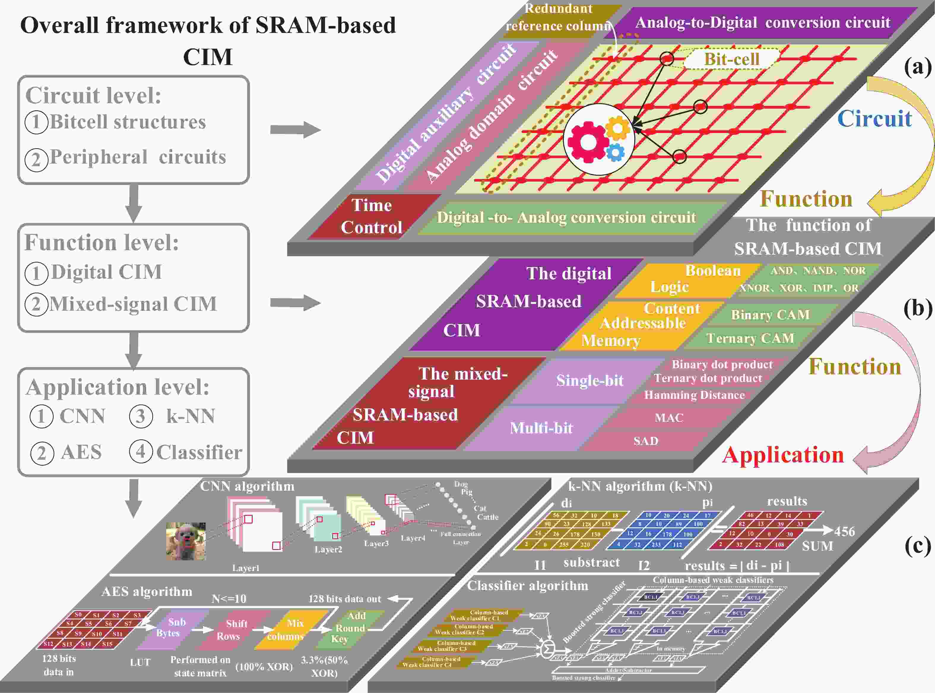
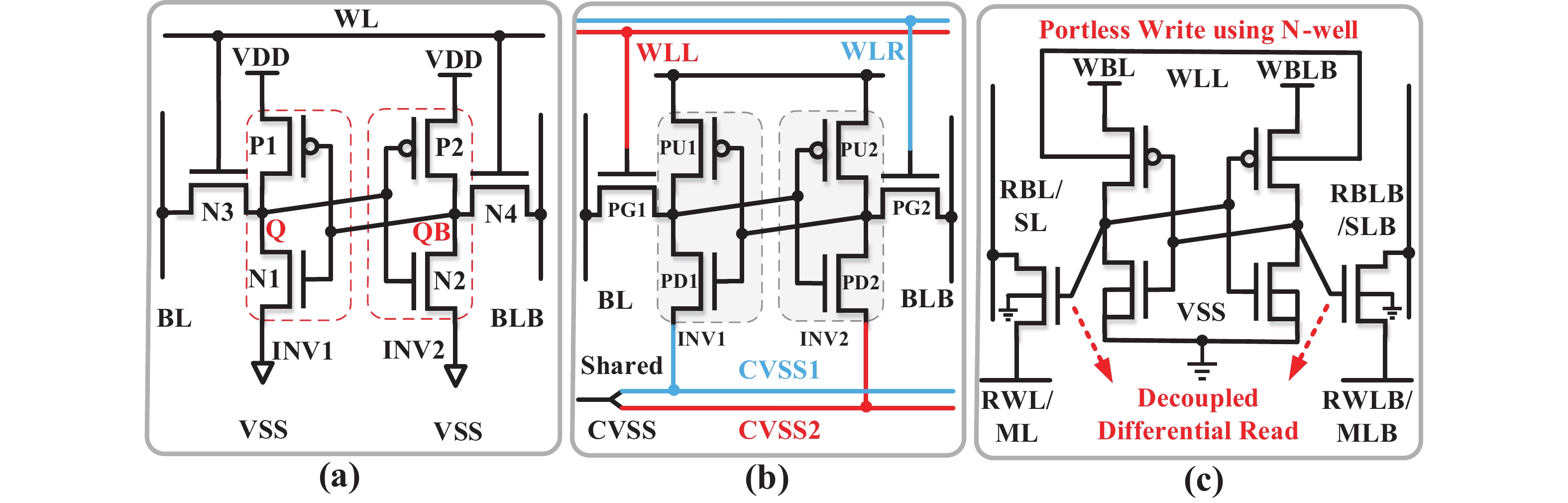
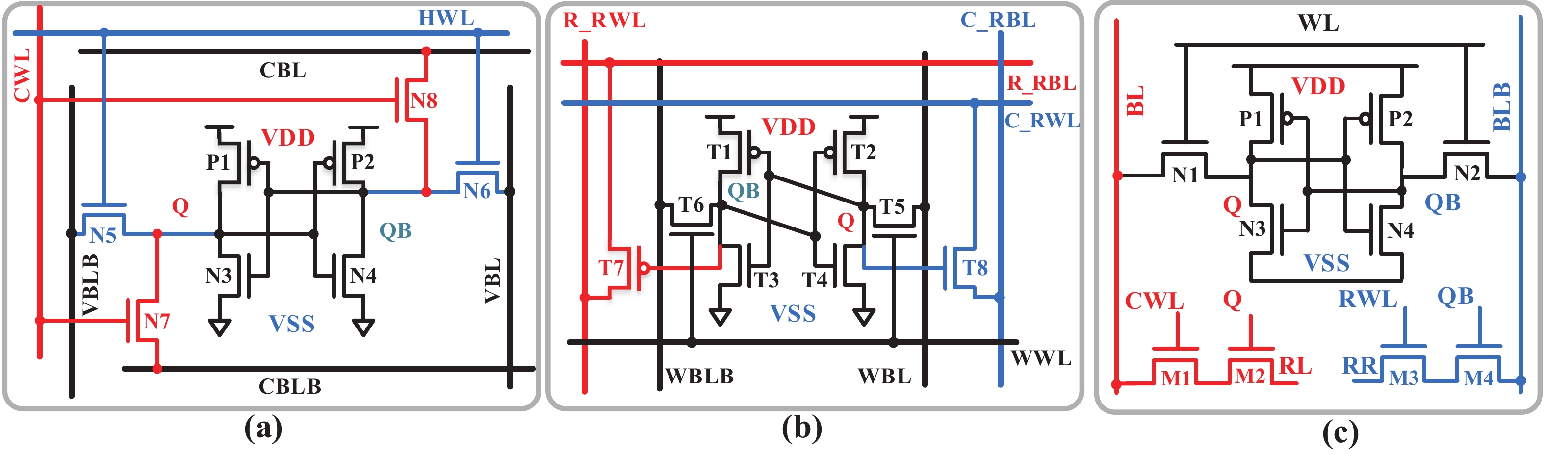
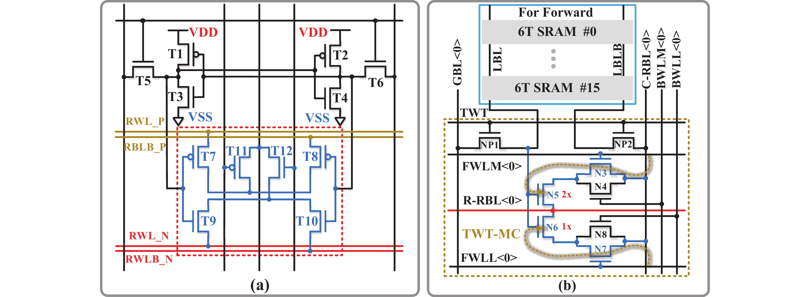
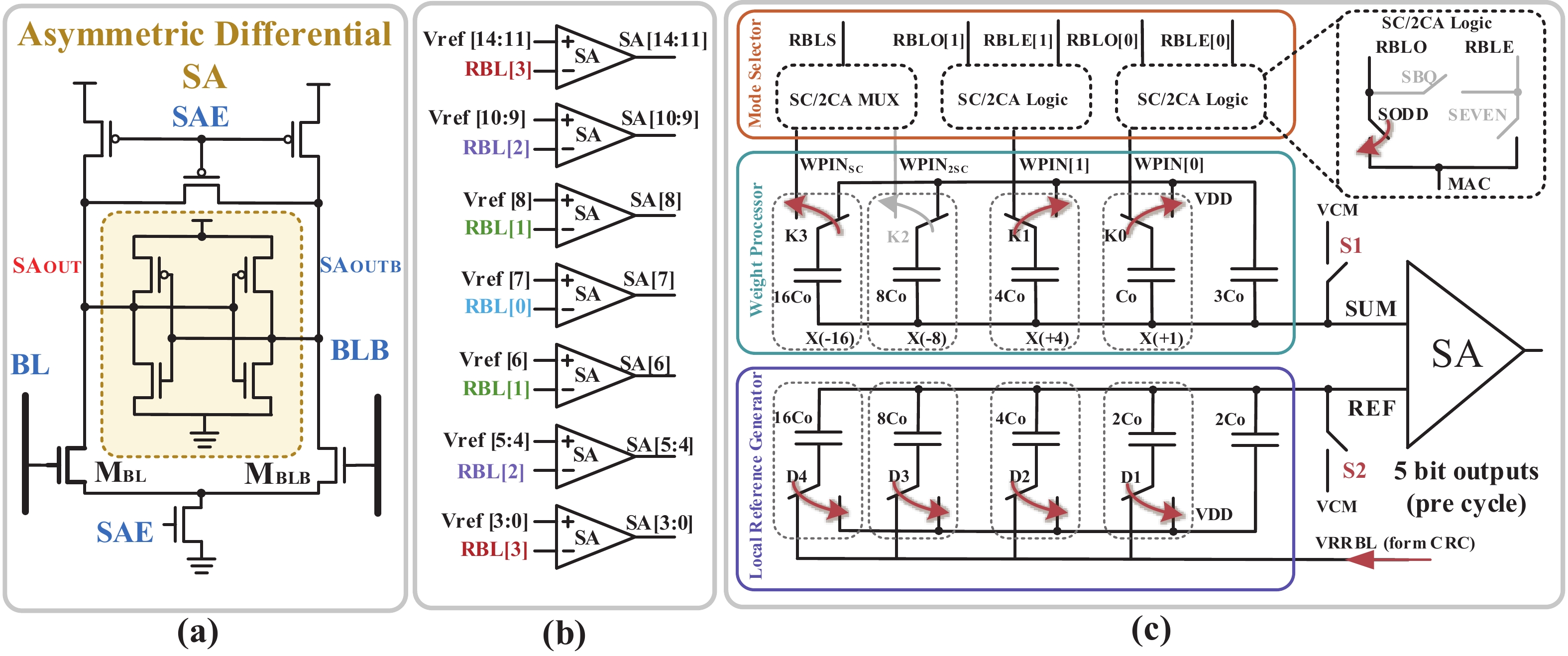
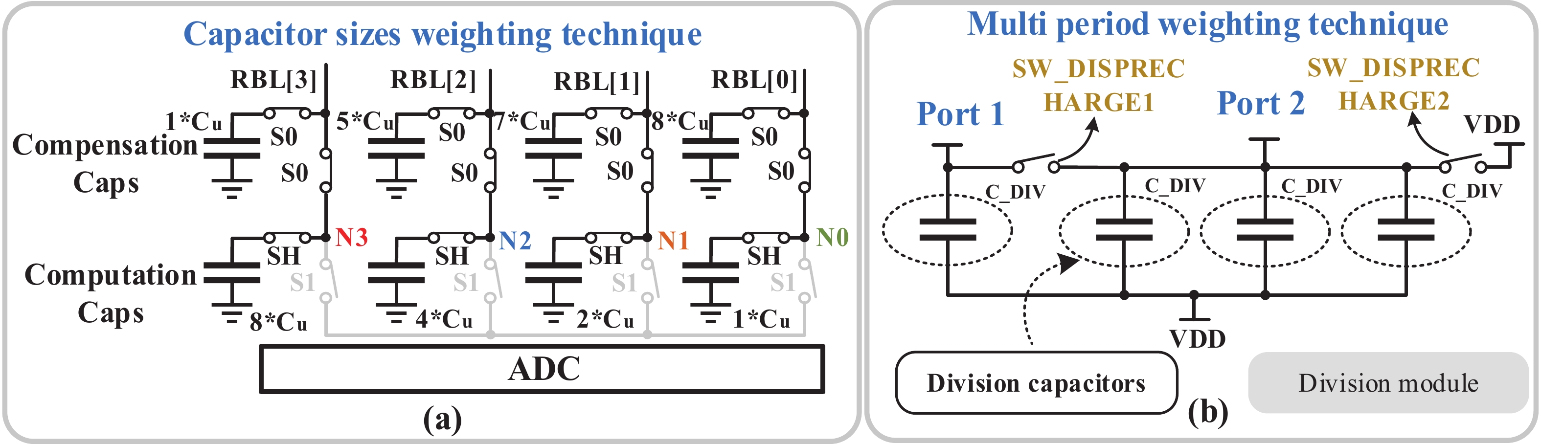
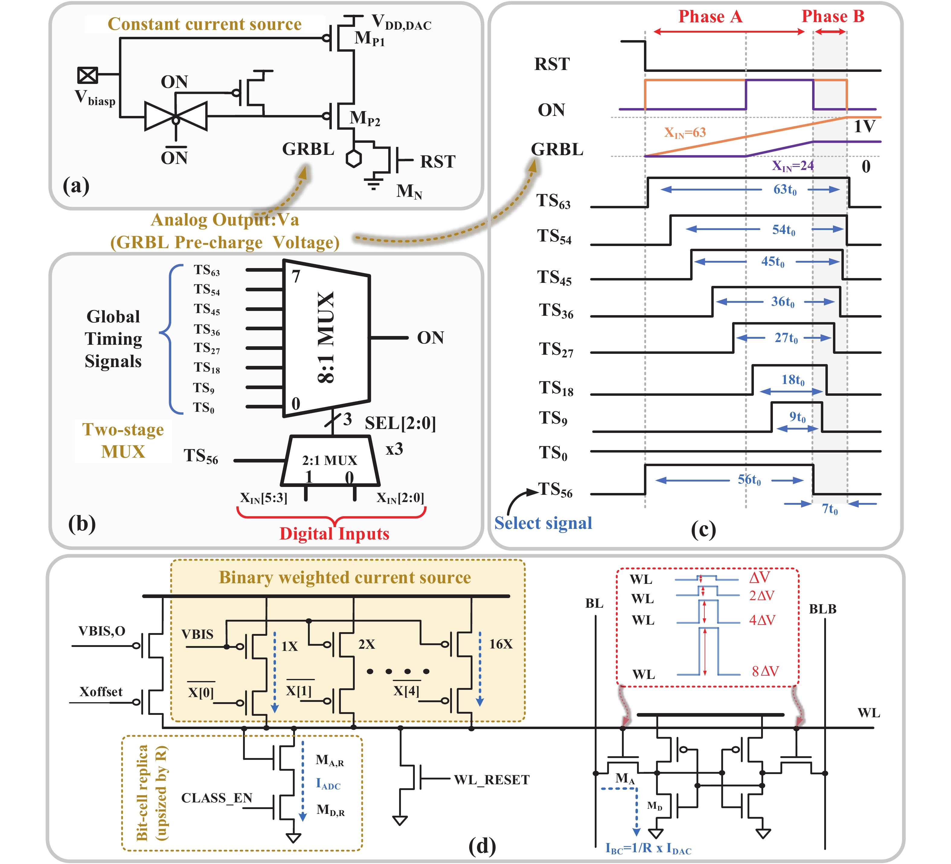
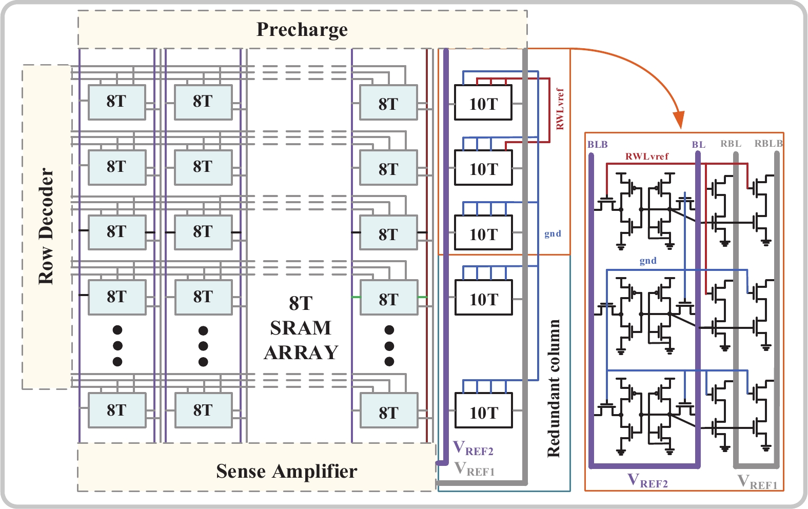
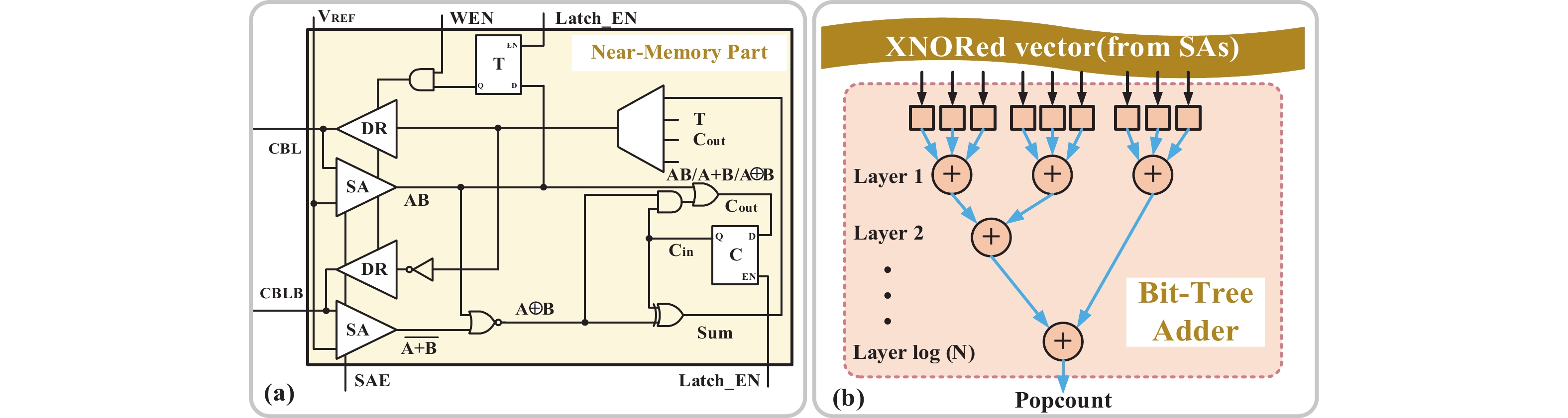
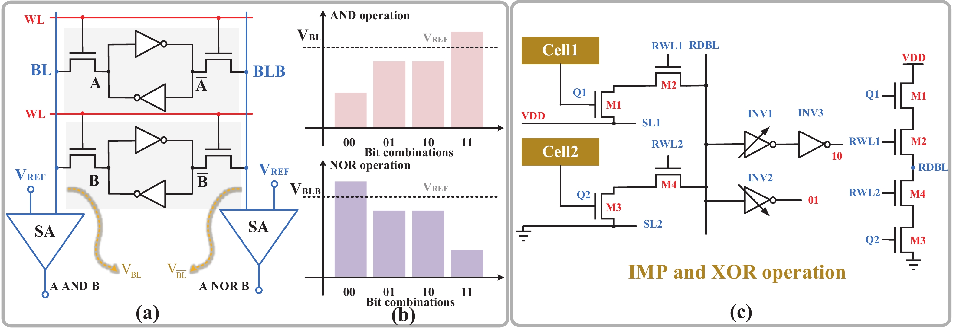
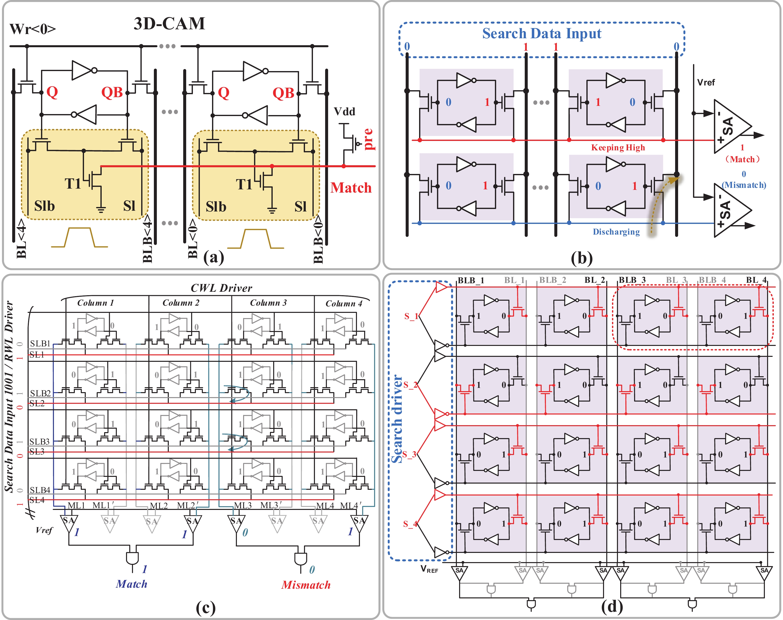
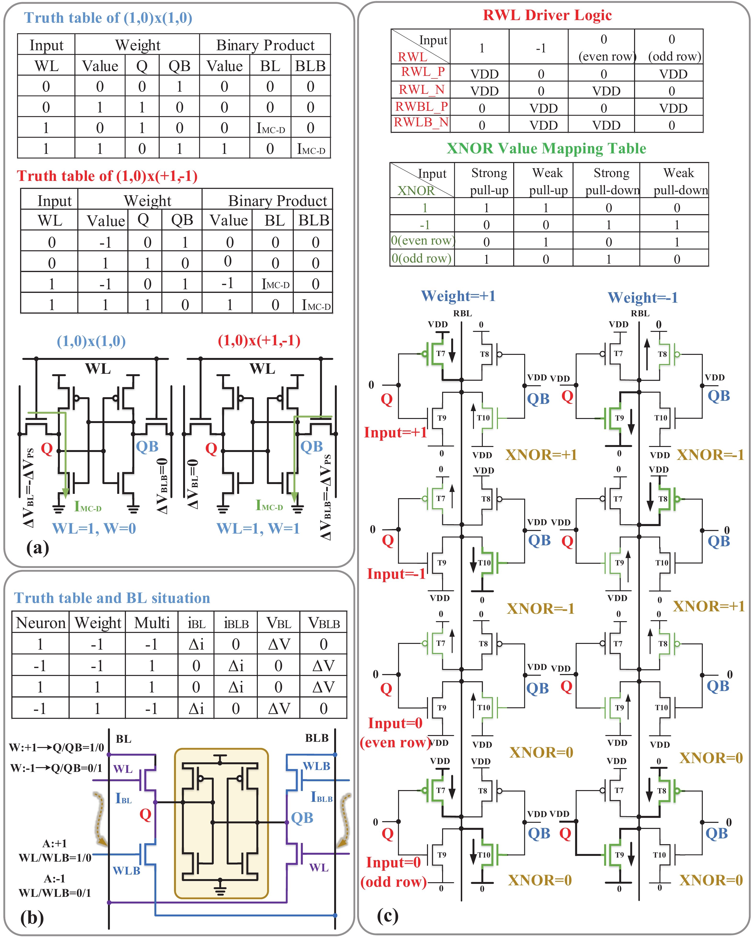
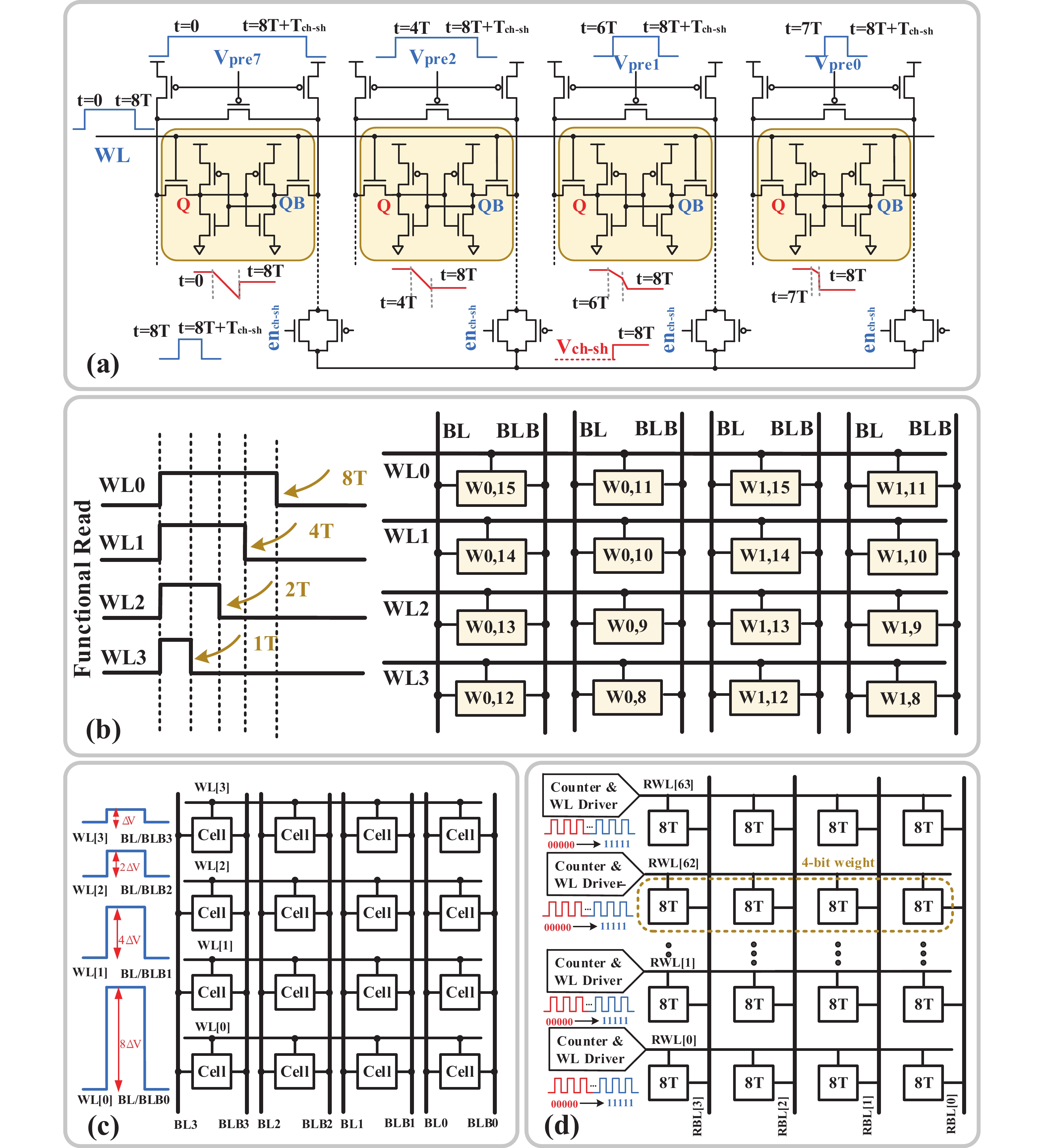
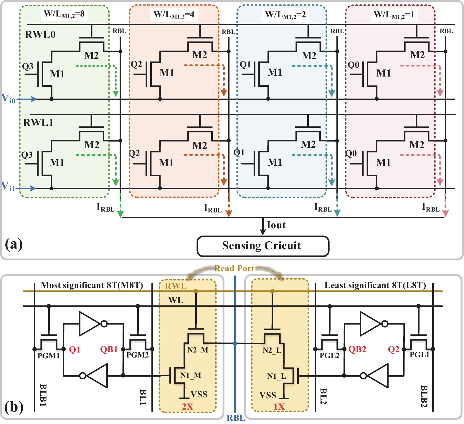
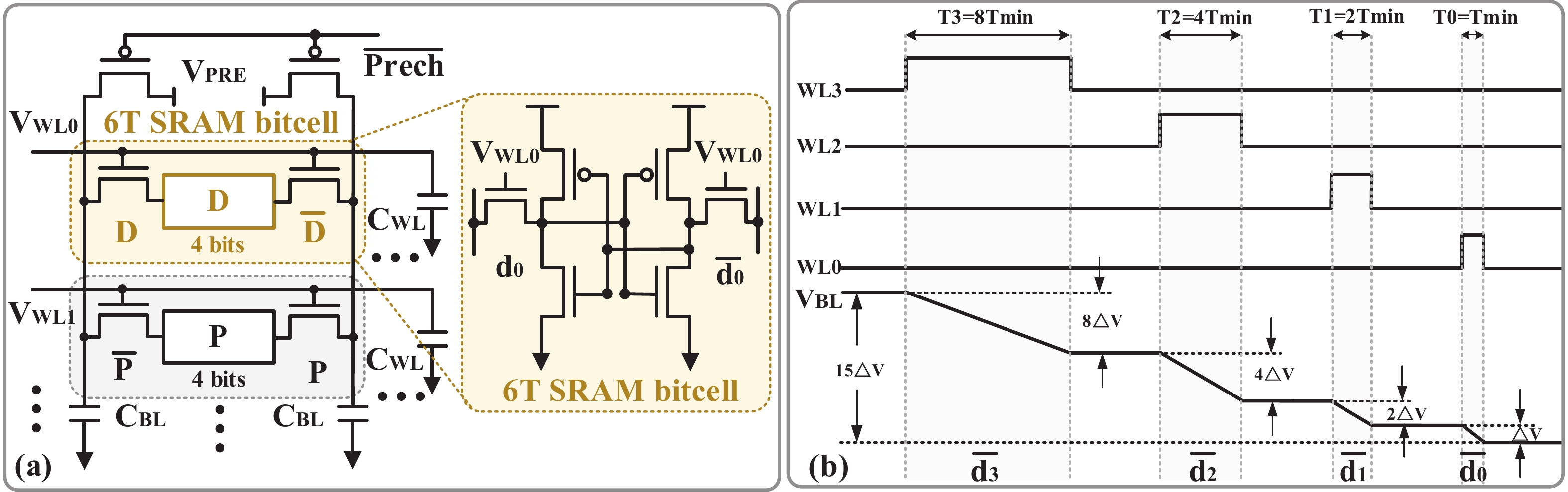
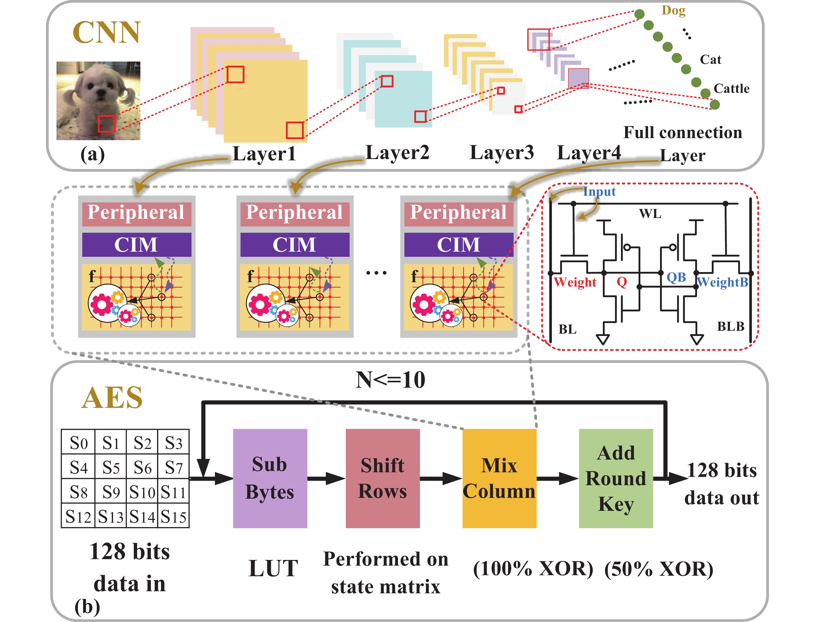
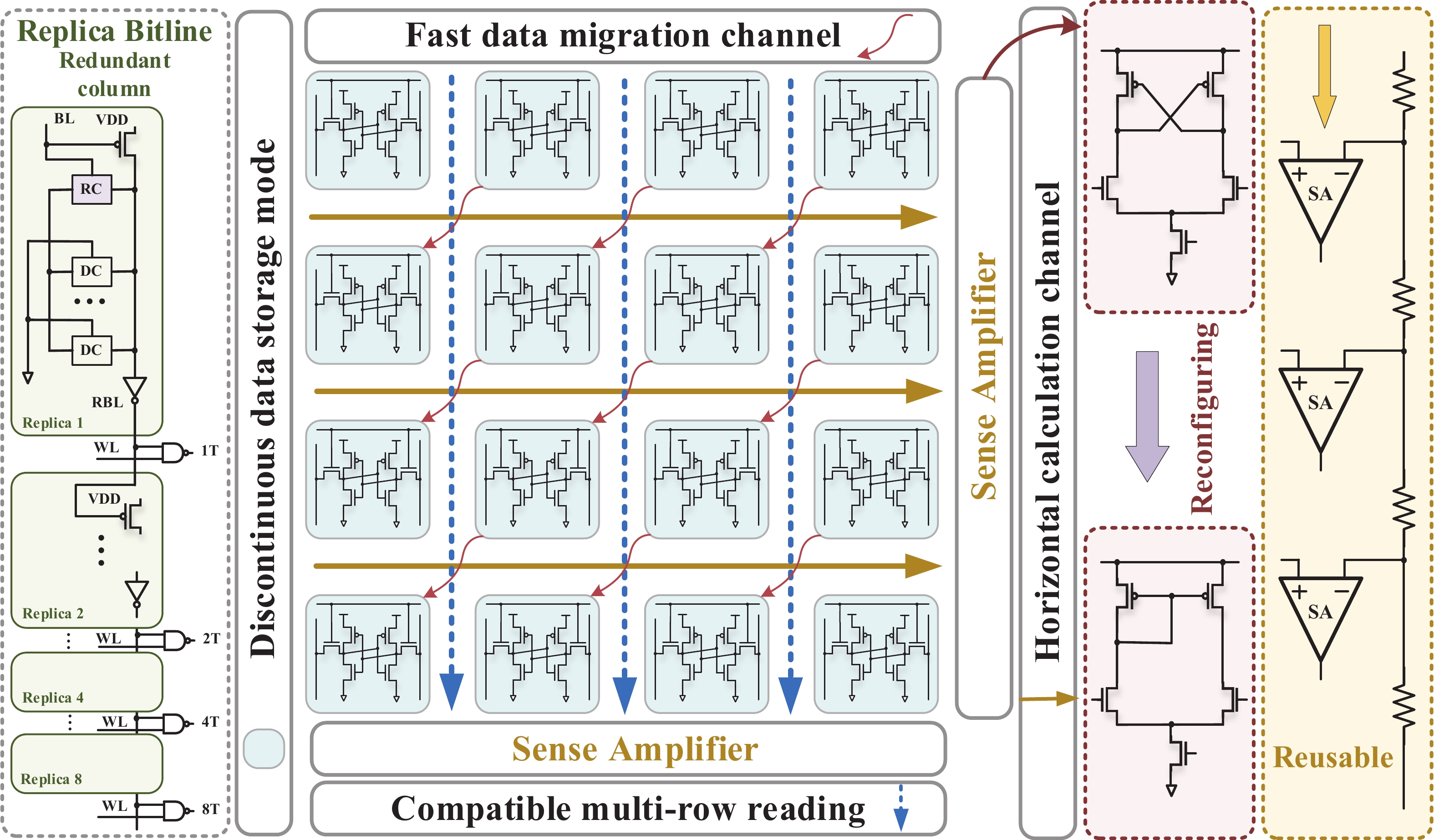
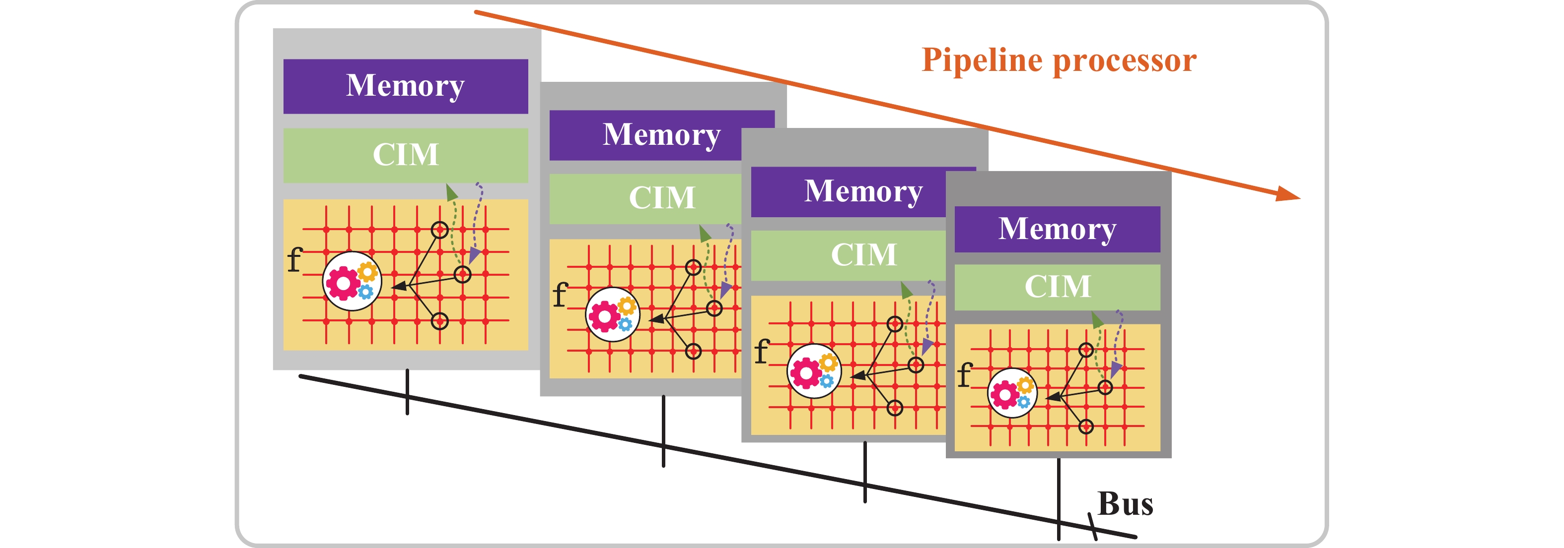
Artificial intelligence (AI) processes data-centric applications with minimal effort. However, it poses new challenges to system design in terms of computational speed and energy efficiency. The traditional von Neumann architecture cannot meet the requirements of heavily data-centric applications due to the separation of computation and storage. The emergence of computing in-memory (CIM) is significant in circumventing the von Neumann bottleneck. A commercialized memory architecture, static random-access memory (SRAM), is fast and robust, consumes less power, and is compatible with state-of-the-art technology. This study investigates the research progress of SRAM-based CIM technology in three levels: circuit, function, and application. It also outlines the problems, challenges, and prospects of SRAM-based CIM macros.


J. Semicond.
2022, 43(3): 032001 doi: 10.1088/1674-4926/43/3/032001
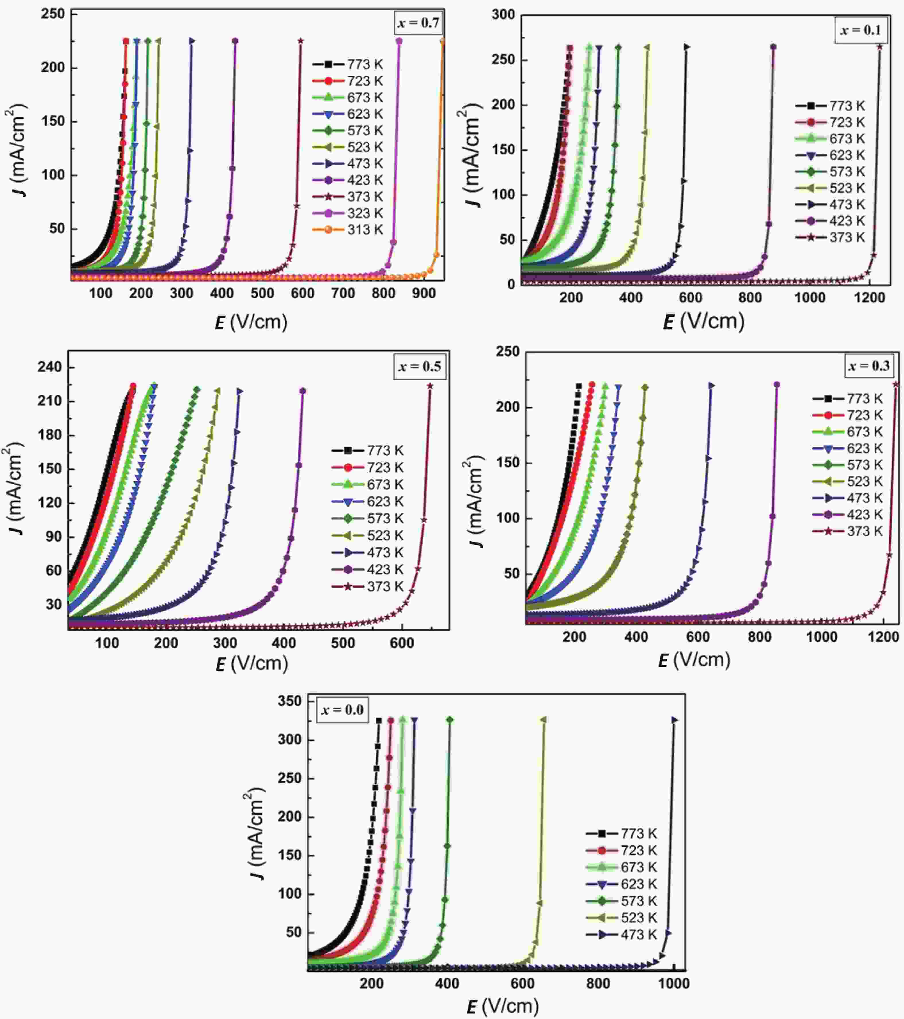
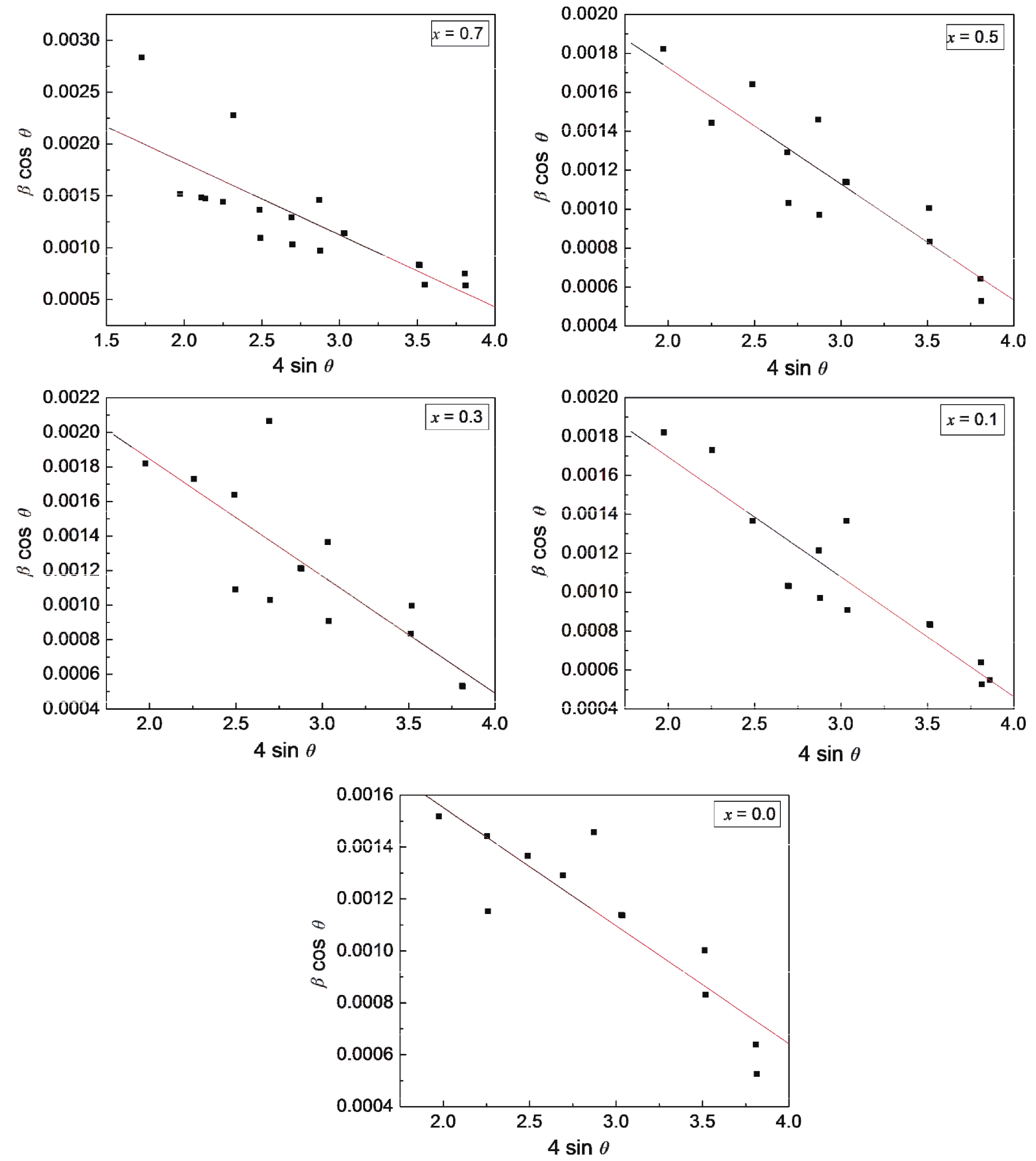
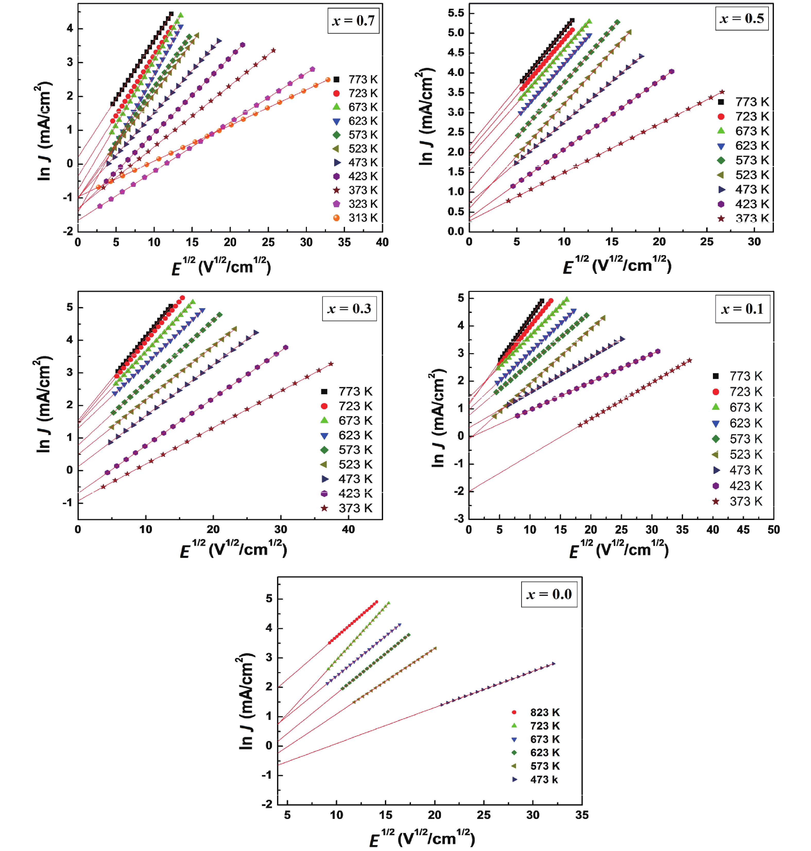
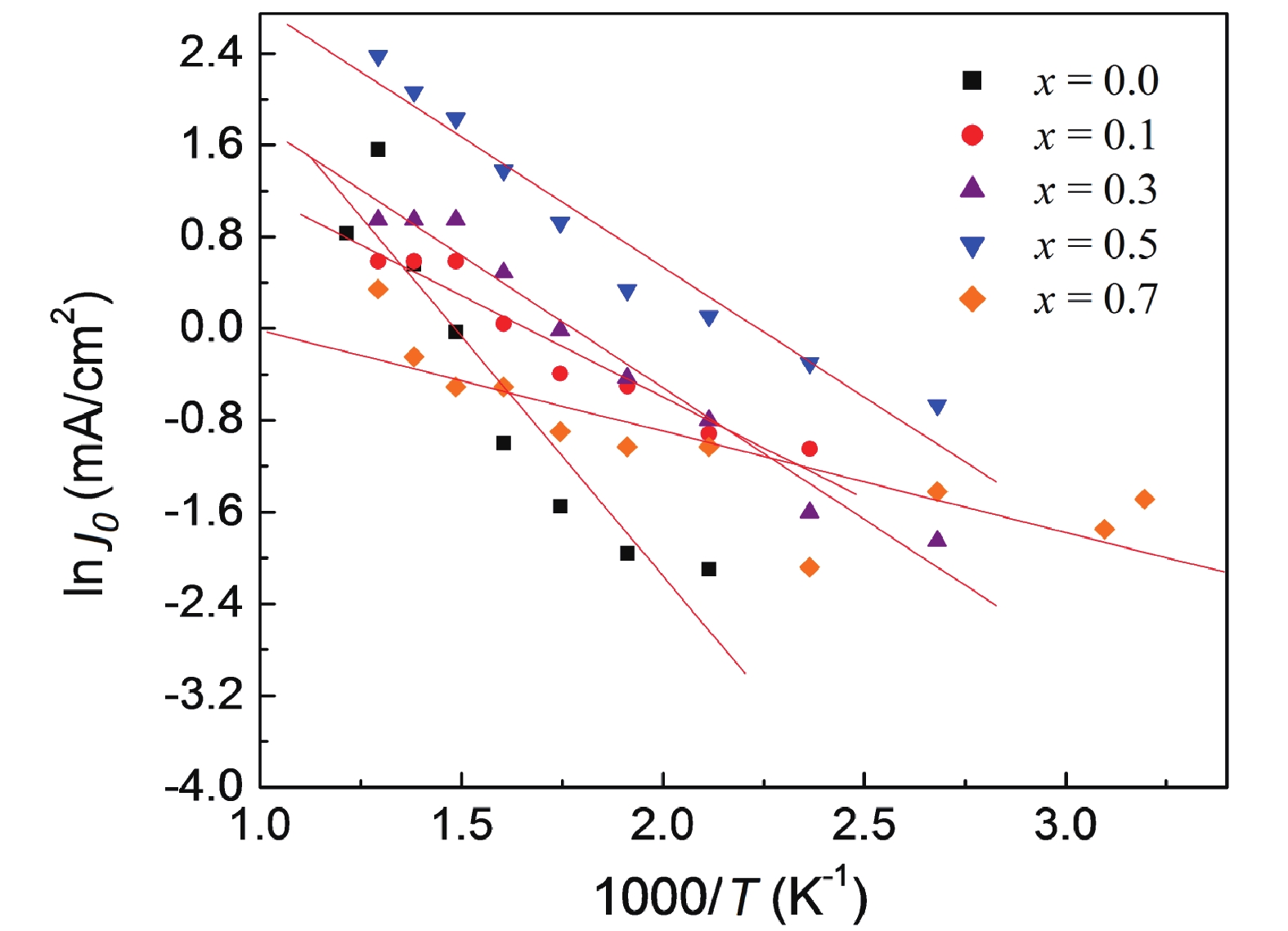
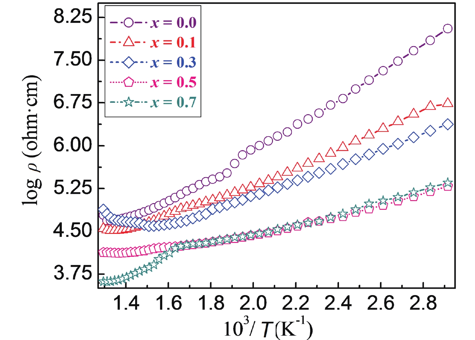
The electrical properties of cubic perovskite series, CaCu3–xTi4–xFe2xO12 with x = 0.0, 0.1, 0.3, 0.5, and 0.7, have been studied by employing current density as a function of electric field characteristics registered at different temperatures and thermal variations of direct current electrical resistivity measurements. All of the compositions exhibit strong non-ohmic behavior. The concentration dependence of breakdown field, the temperature at which switching action takes place, and maximum value of current density (Jmax) has been explained on account of structural, microstructural, and positron lifetime parameters. The highest ever reported value of Jmax = 327 mA/cm2 has been observed for pristine composition. The values of the nonlinear coefficient advise the suitability of ceramics for low-voltage varistor applications. The Arrhenius plots show typical semiconducting nature. The activation energy values indicate that electric conduction proceeds through electrons with deformation in the system.
J. Semicond.
2022, 43(3): 032401 doi: 10.1088/1674-4926/43/3/032401
A proposed inductive-phase-compensation ultra wideband CMOS digital T-type attenuator design based on an analysis of minimising phase errors is presented in this letter. In a standard CMOS technology, the proposed attenuator is analytically demonstrated to have low phase errors due to the inductive-phase-compensation network. A design equation is inferred and a wide-band 4dB attenuation bit digital attenuator with low phase errors is designed as a test vehicle for the proposed approach.


J. Semicond.
2022, 43(3): 032402 doi: 10.1088/1674-4926/43/3/032402
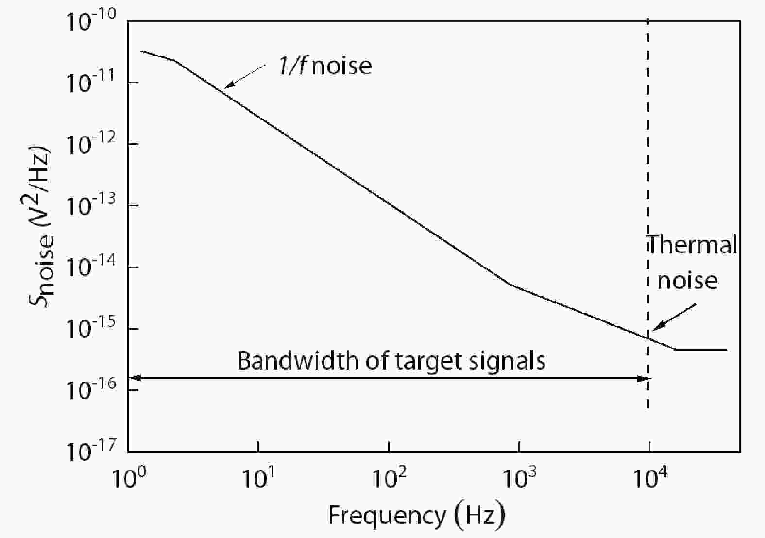
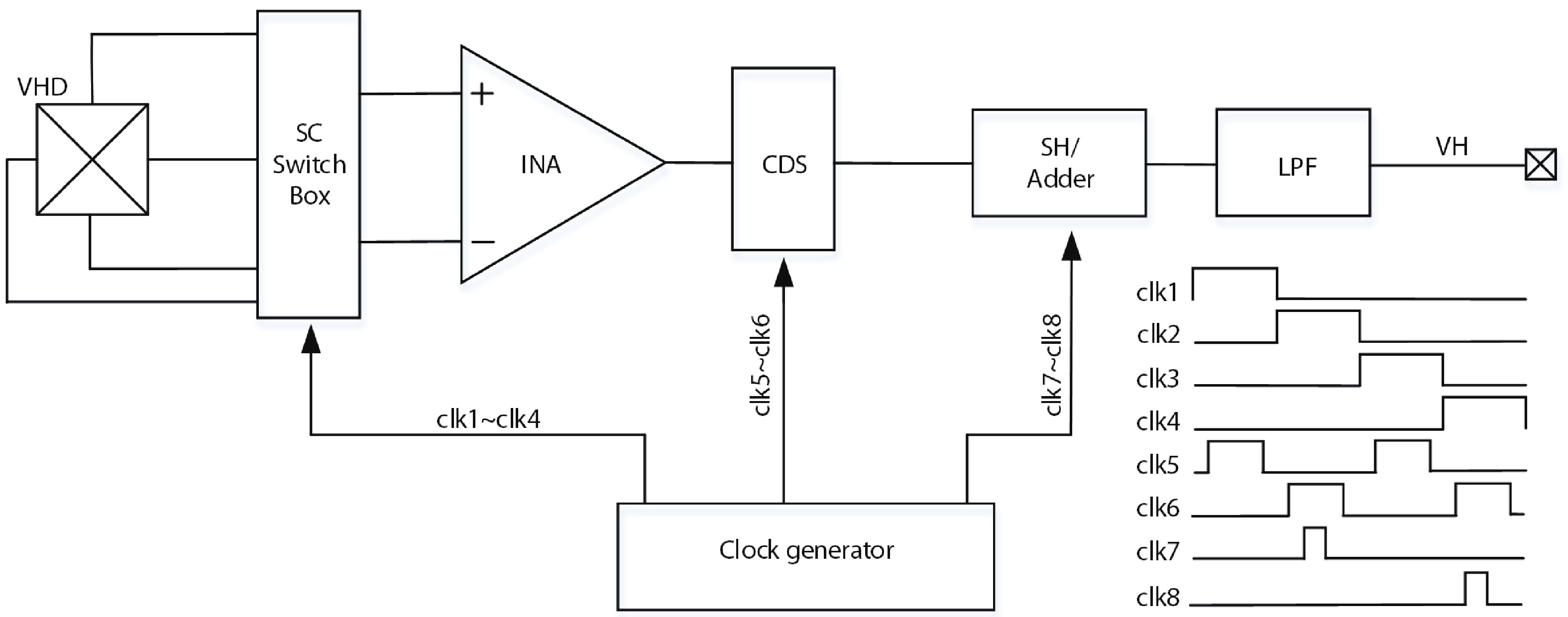
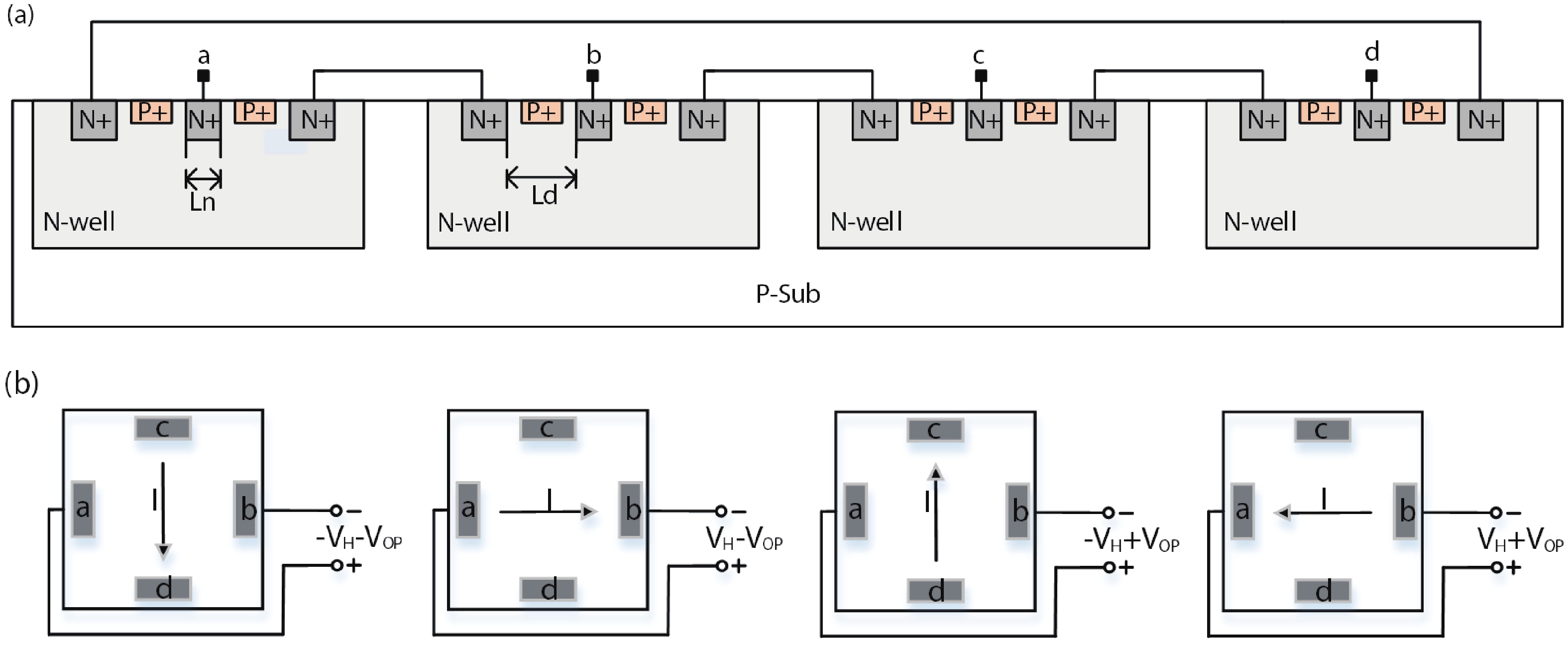
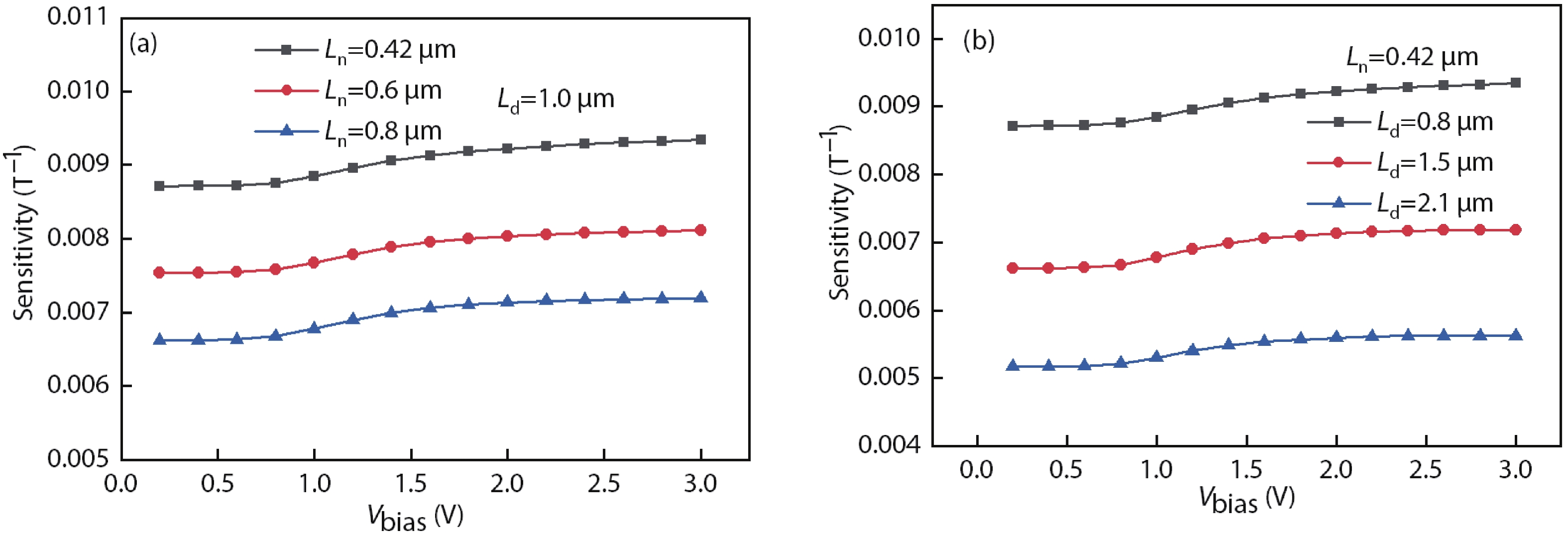
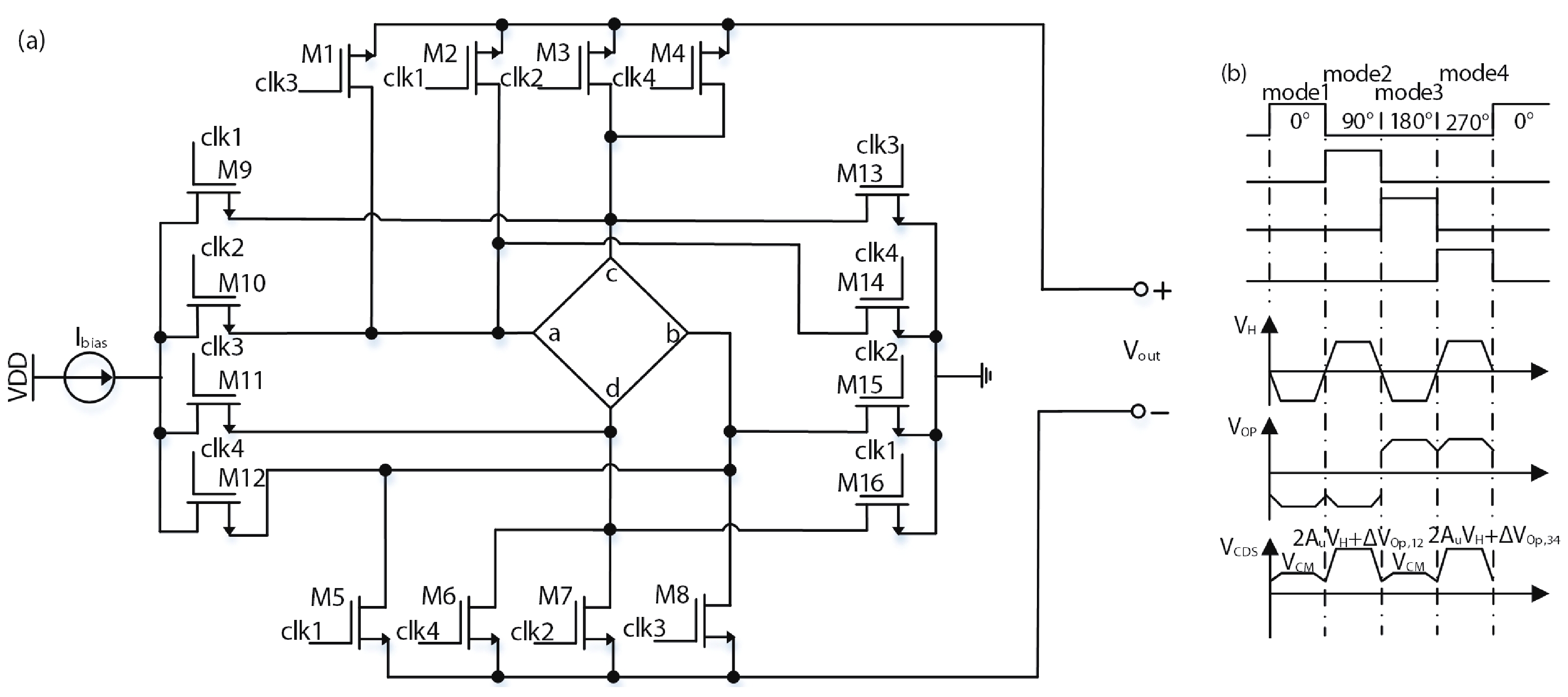
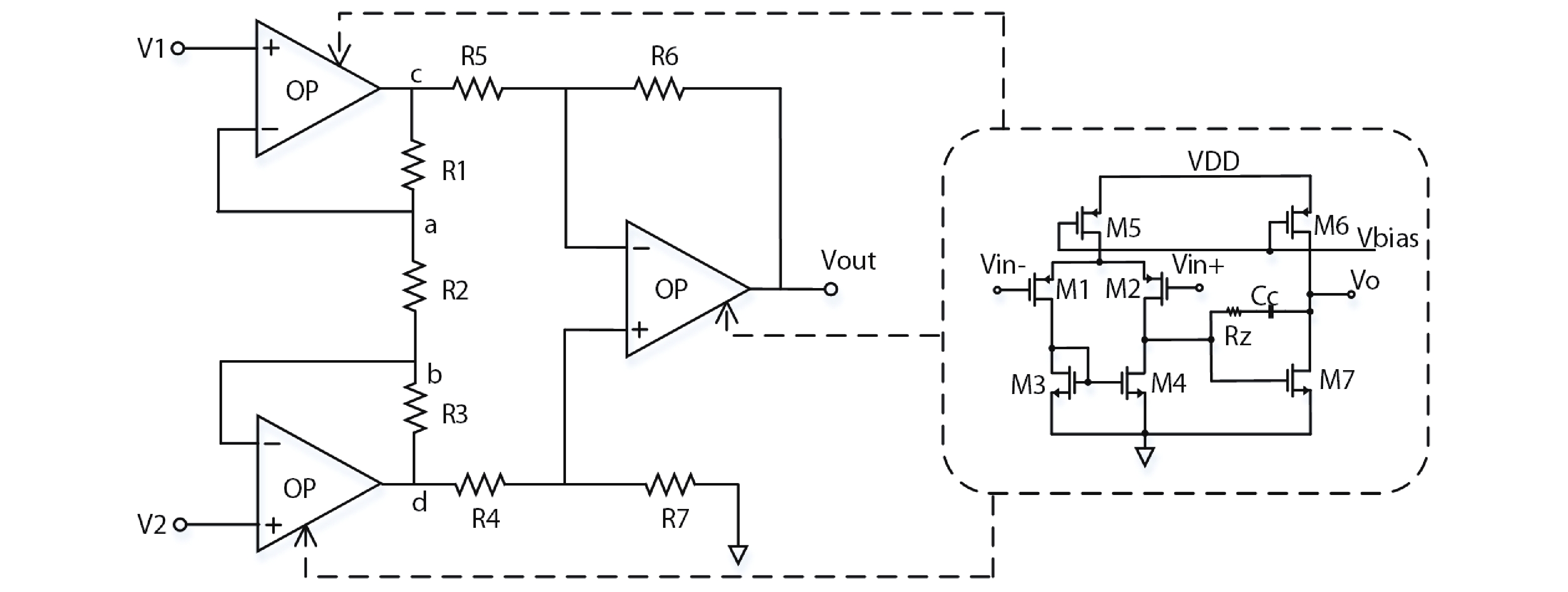
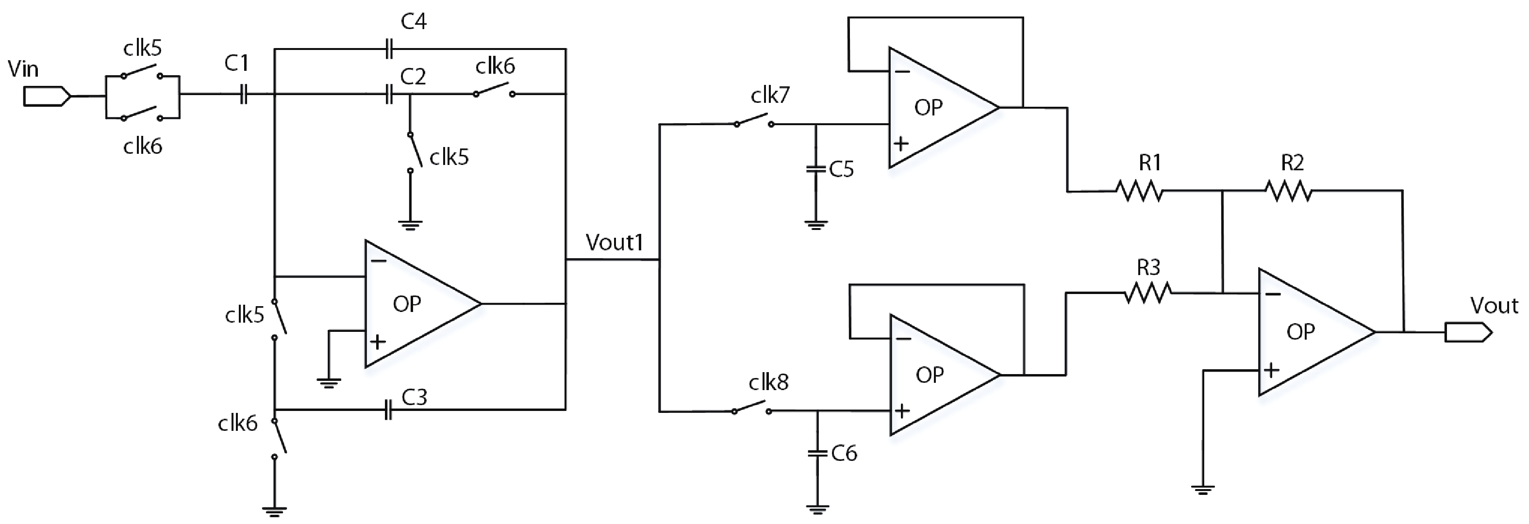
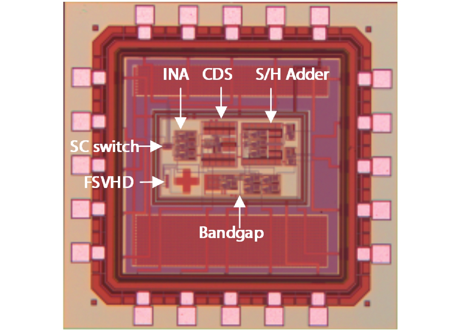
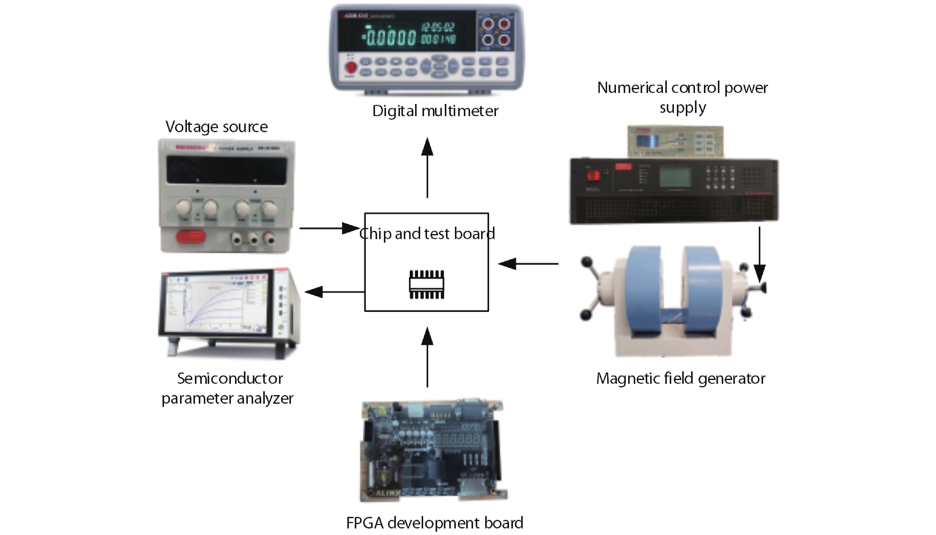
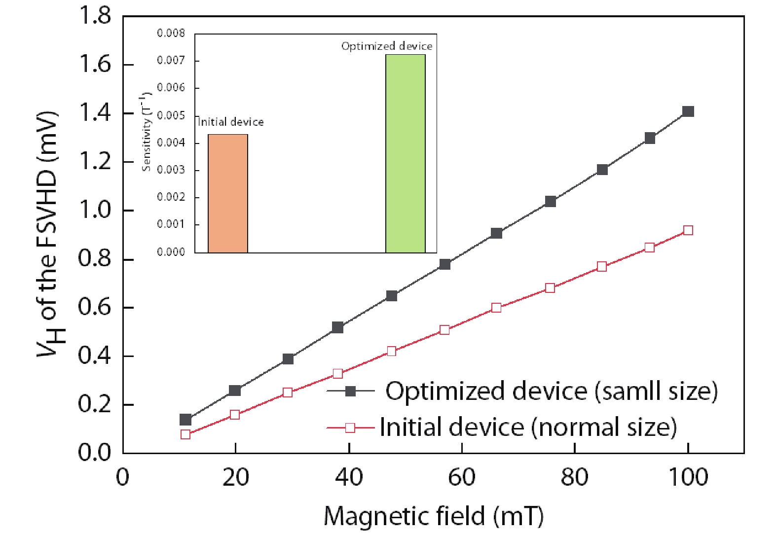
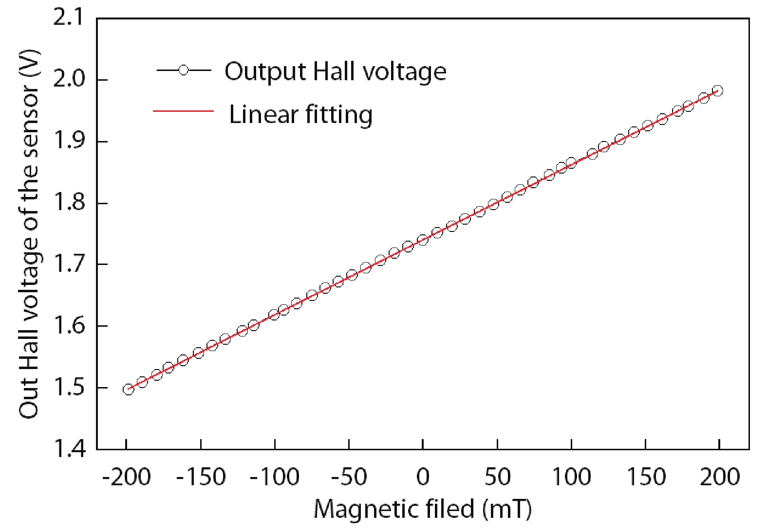
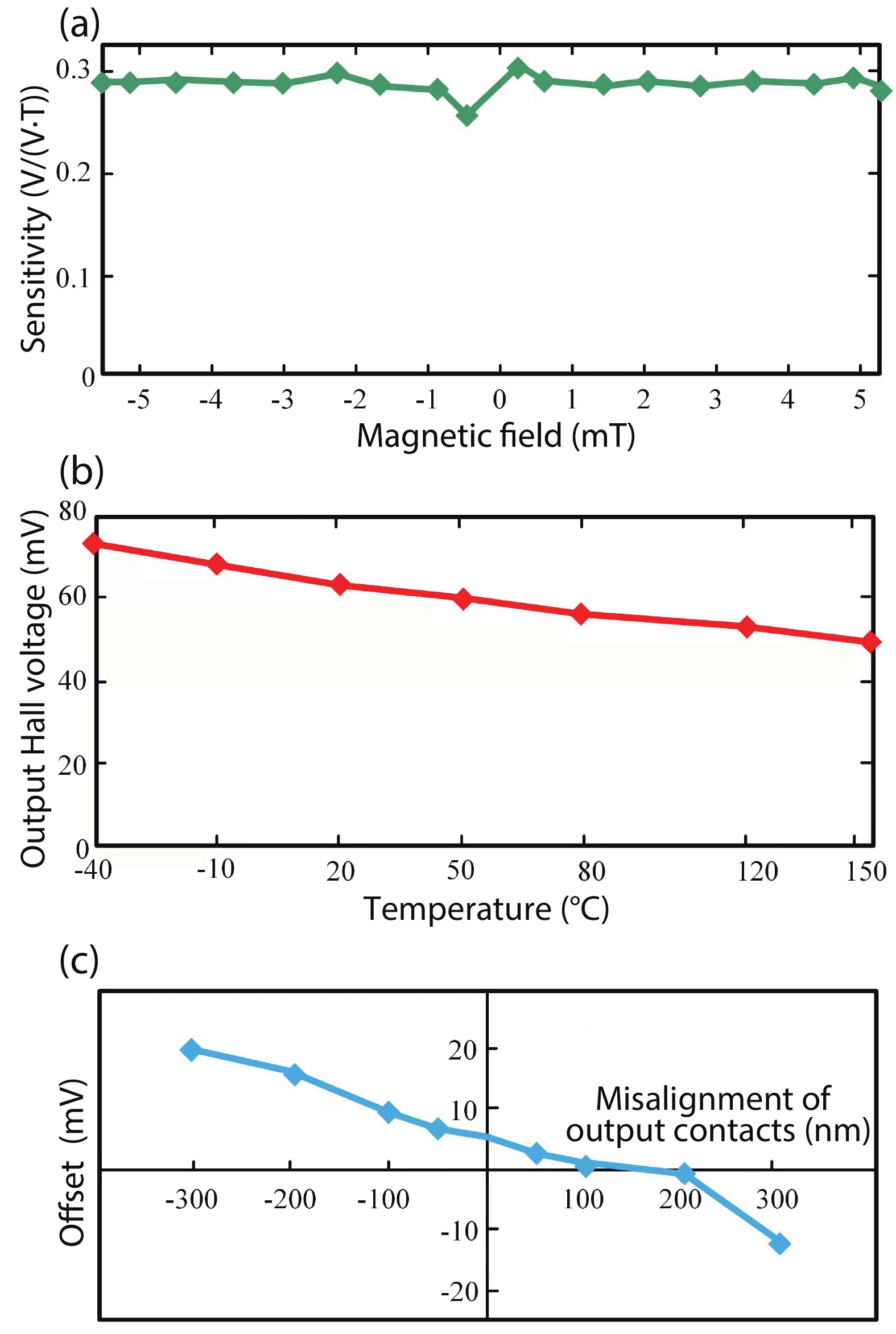
An integrated front-end vertical CMOS Hall magnetic sensor is proposed for the in-plane magnetic field measurement. To improve the magnetic sensitivity and to obtain low offset, a fully symmetric vertical Hall device (FSVHD) has been optimized with a minimum size design. A new four-phase spinning current modulation associated with a correlated double sampling (CDS) demodulation technique has been further applied to compensate for the offset and also to provide a linear Hall output voltage. The vertical Hall sensor chip has been manufactured in a 0.18 μm low-voltage CMOS technology and it occupies an area of 1.54 mm2. The experimental results show in the magnetic field range from –200 to 200 mT, the entire vertical Hall sensor performs with the linearity of 99.9% and the system magnetic sensitivity of 1.22 V/T and the residual offset of 60 μT. Meanwhile, it consumes 4.5 mW at a 3.3 V supply voltage. The proposed vertical Hall sensor is very suitable for the low-cost system-on-chip (SOC) implementation of 2D or 3D magnetic microsystems.


J. Semicond.
2022, 43(3): 032701 doi: 10.1088/1674-4926/43/3/032701
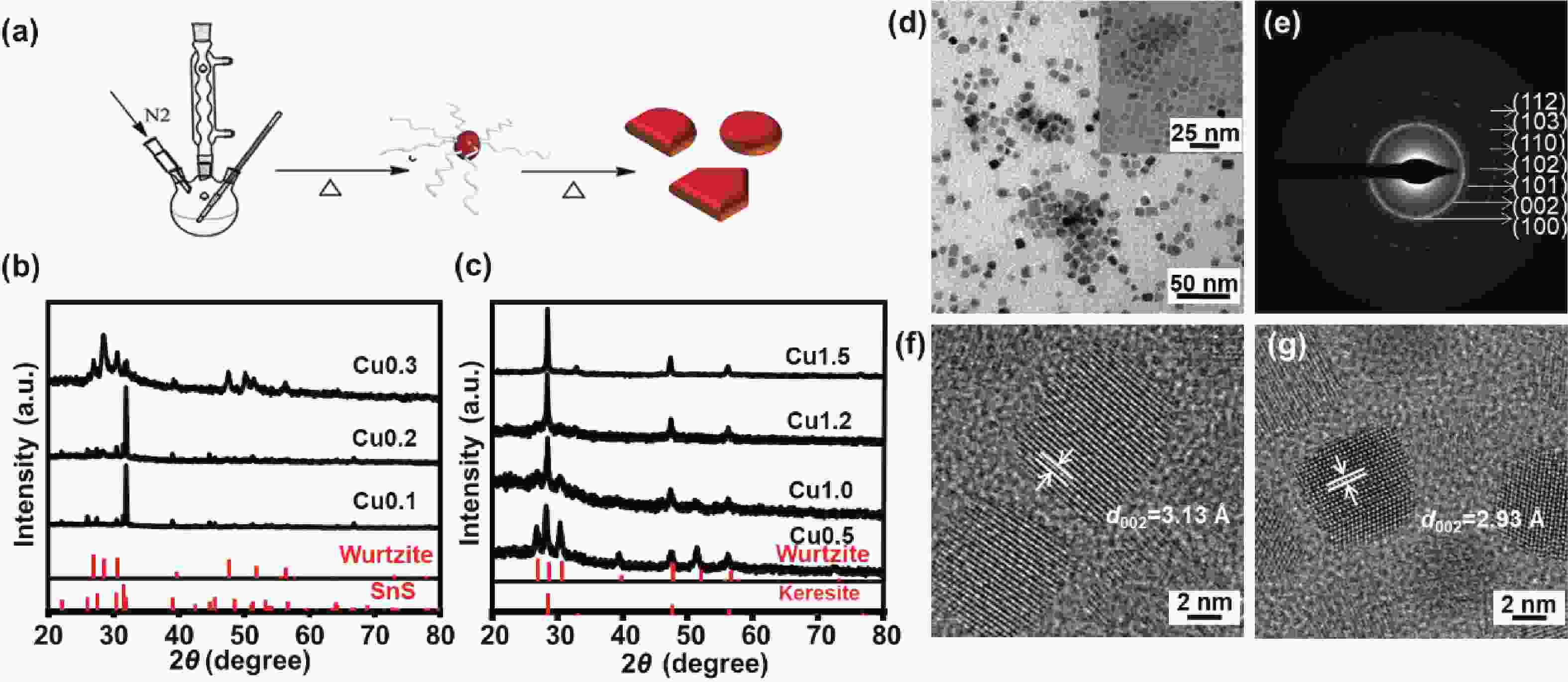
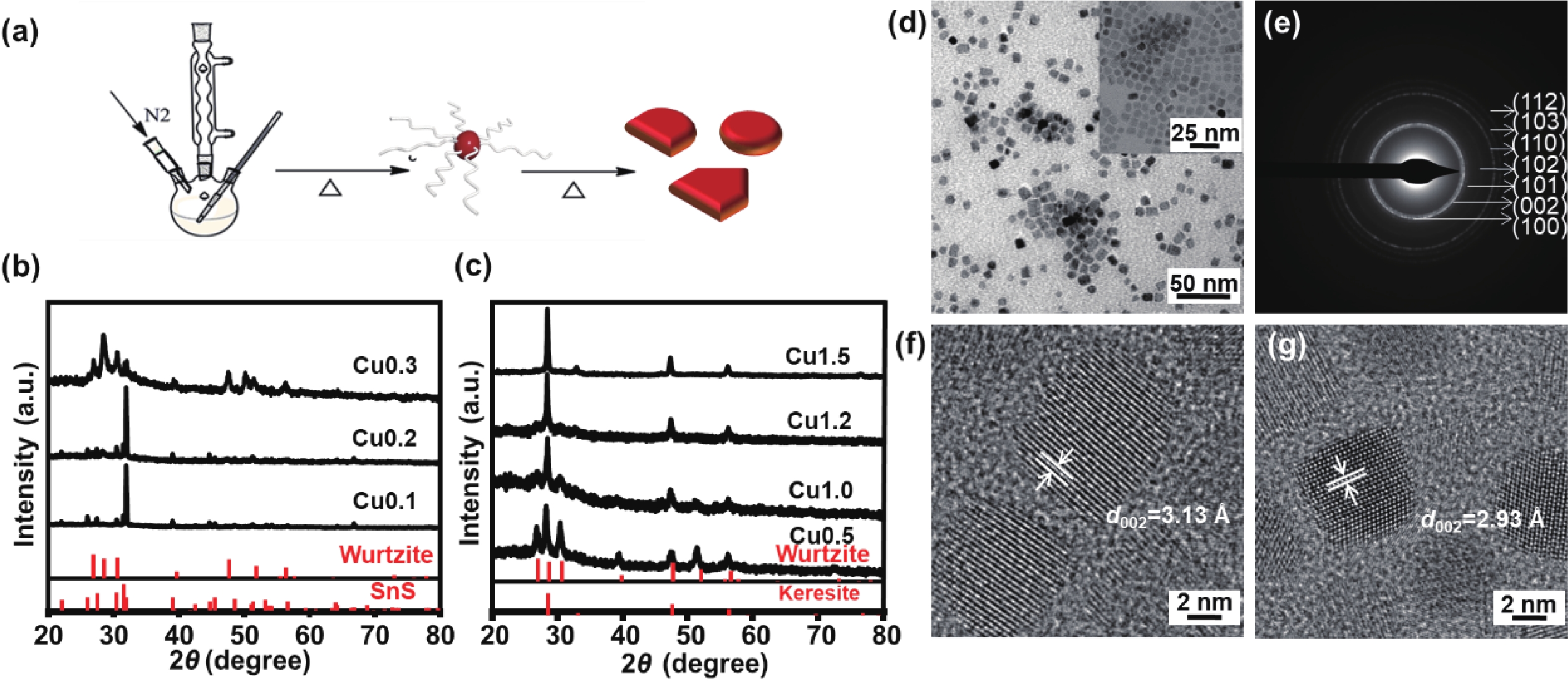
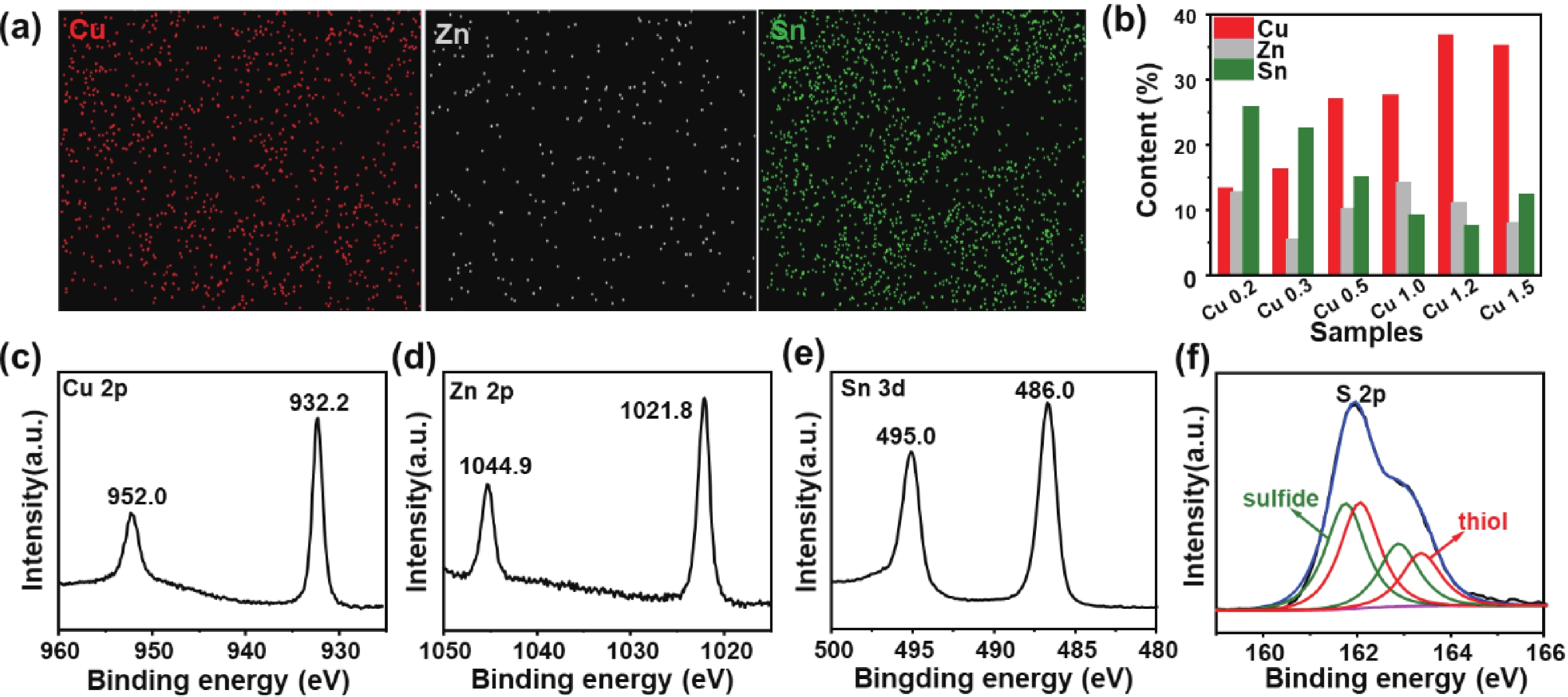
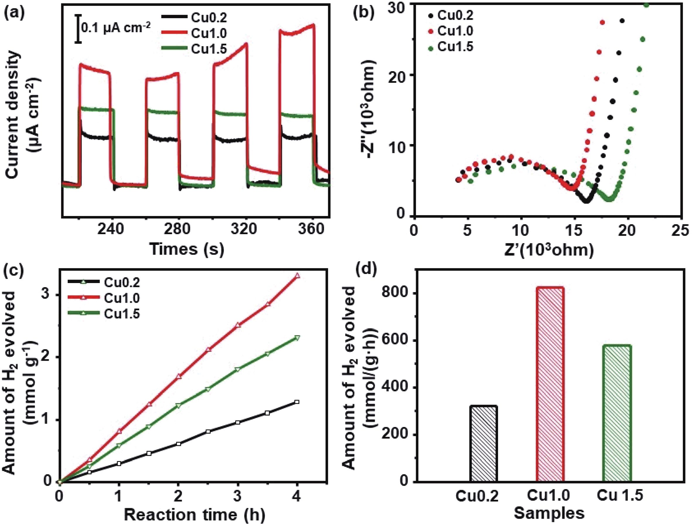
Hydrogen energy is a powerful and efficient energy resource, which can be produced by photocatalytic water splitting. Among the photocatalysis, multinary copper-based chalcogenide semiconductor nanocrystals exhibit great potential due to their tunable crystal structures, adjustable optical band gap, eco-friendly, and abundant resources. In this paper, Cu–Zn–Sn–S (CZTS) nanocrystals with different Cu content have been synthesized by using the one-pot method. By regulating the surface ligands, the reaction temperature, and the Cu content, kesterite and hexagonal wurtzite CZTS nanocrystals were obtained. The critical factors for the controllable transition between two phases were discussed. Subsequently, a series of quaternary CZTS nanocrystals with different Cu content were used for photocatalytic hydrogen evolution. And their band gap, energy level structure, and charge transfer ability were compared comprehensively. As a result, the pure hexagonal wurtzite CZTS nanocrystals have exhibited an improved photocatalytic hydrogen evolution activity.

J. Semicond.
2022, 43(3): 032801 doi: 10.1088/1674-4926/43/3/032801
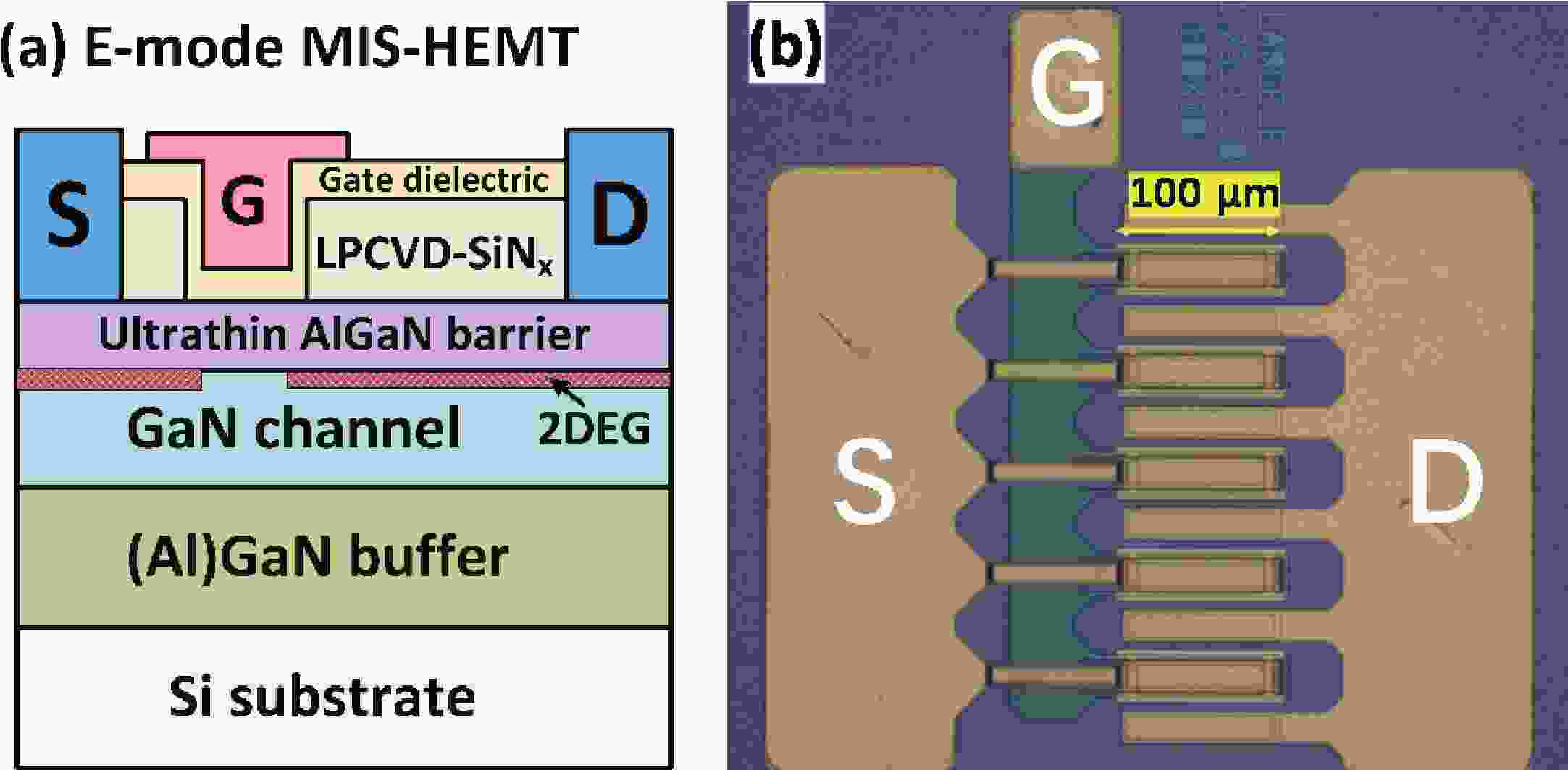
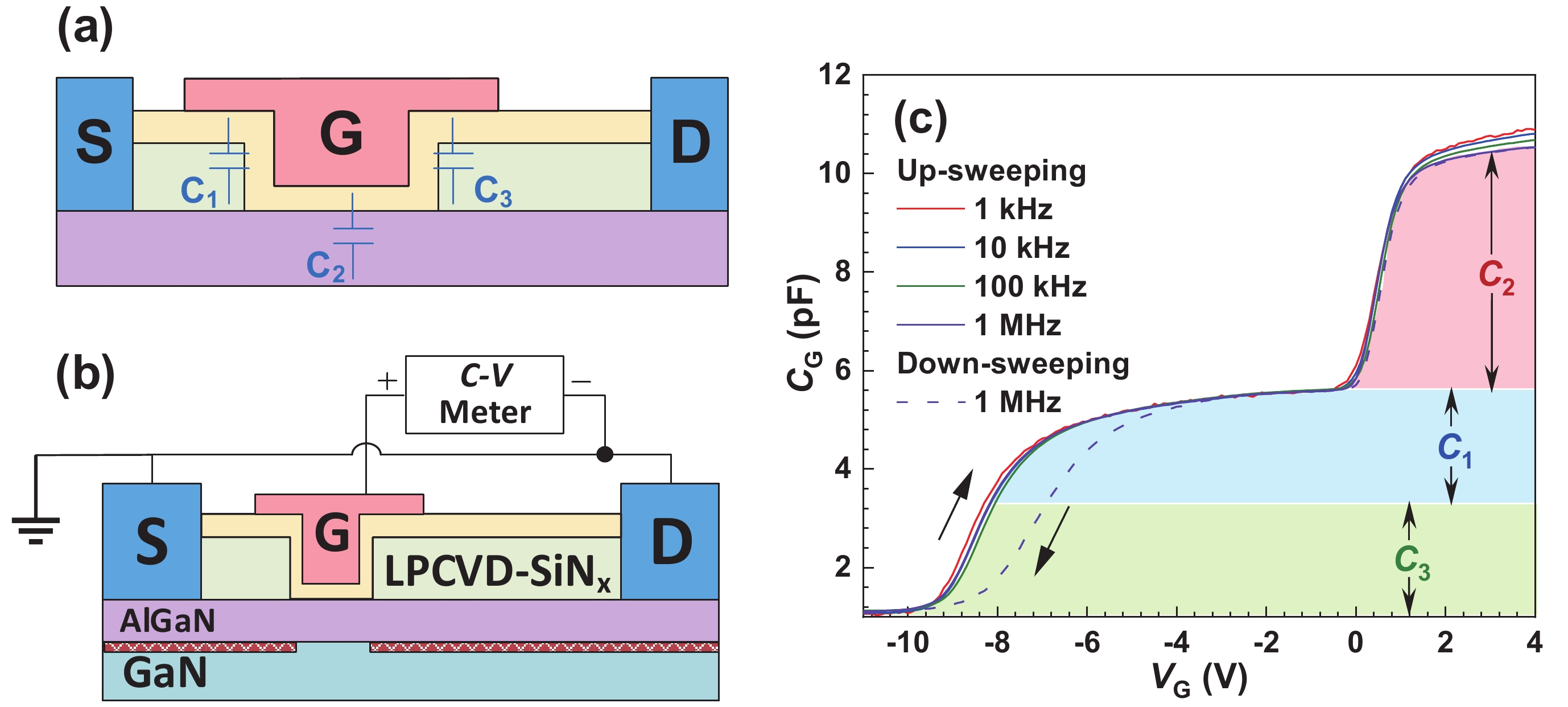
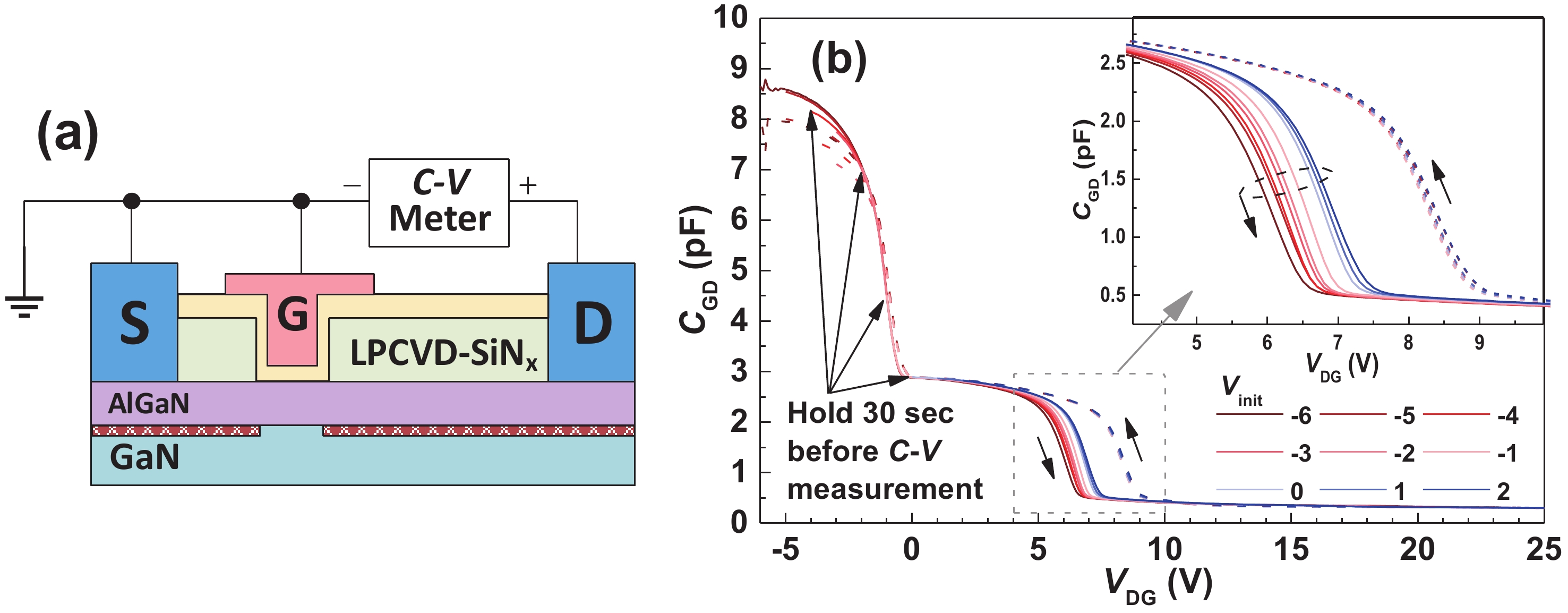
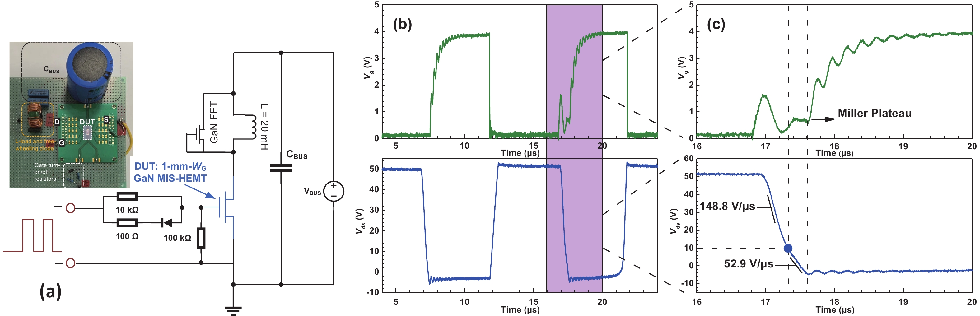
Parasitic capacitances associated with overhangs of the T-shape-gate enhancement-mode (E-mode) GaN-based power device, were investigated by frequency/voltage-dependent capacitance–voltage and inductive-load switching measurements. The overhang capacitances induce a pinch-off voltage distinguished from that of the E-mode channel capacitance in the gate capacitance and the gate–drain capacitance characteristic curves. Frequency- and voltage-dependent tests confirm the instability caused by the trapping of interface/bulk states in the LPCVD-SiNx passivation dielectric. Circuit-level double pulse measurement also reveals its impact on switching transition for power switching applications.


J. Semicond.
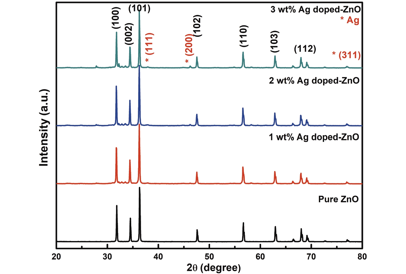
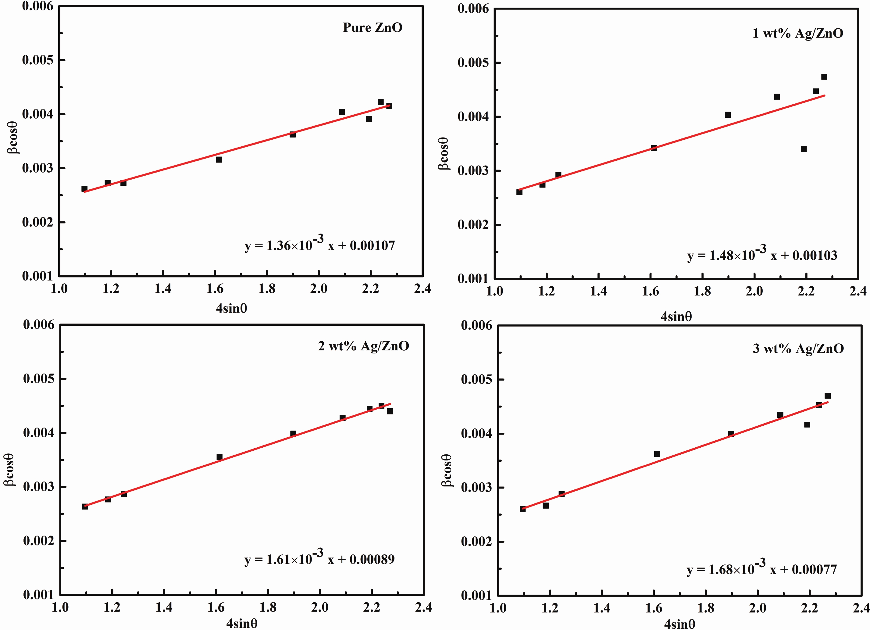
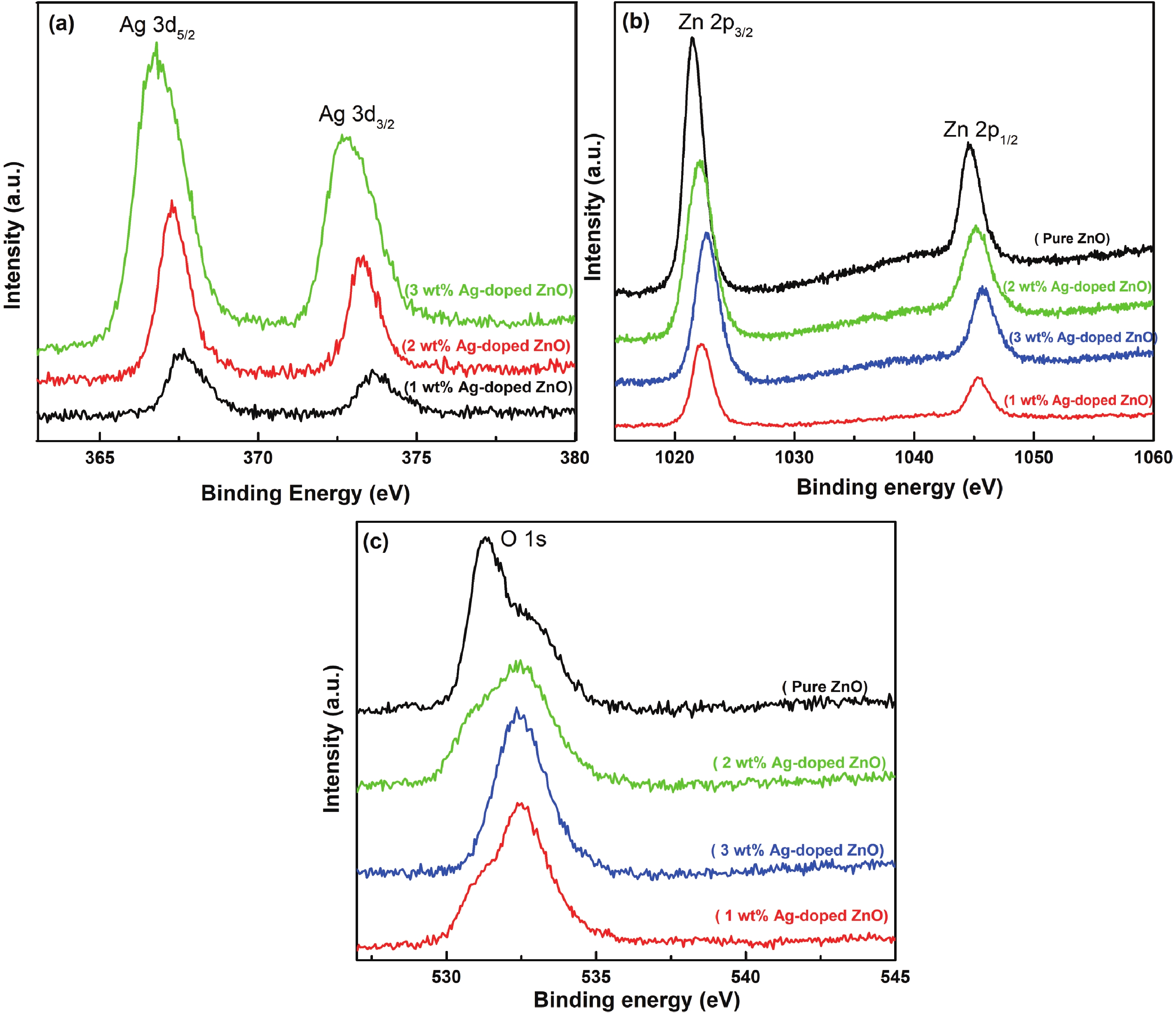
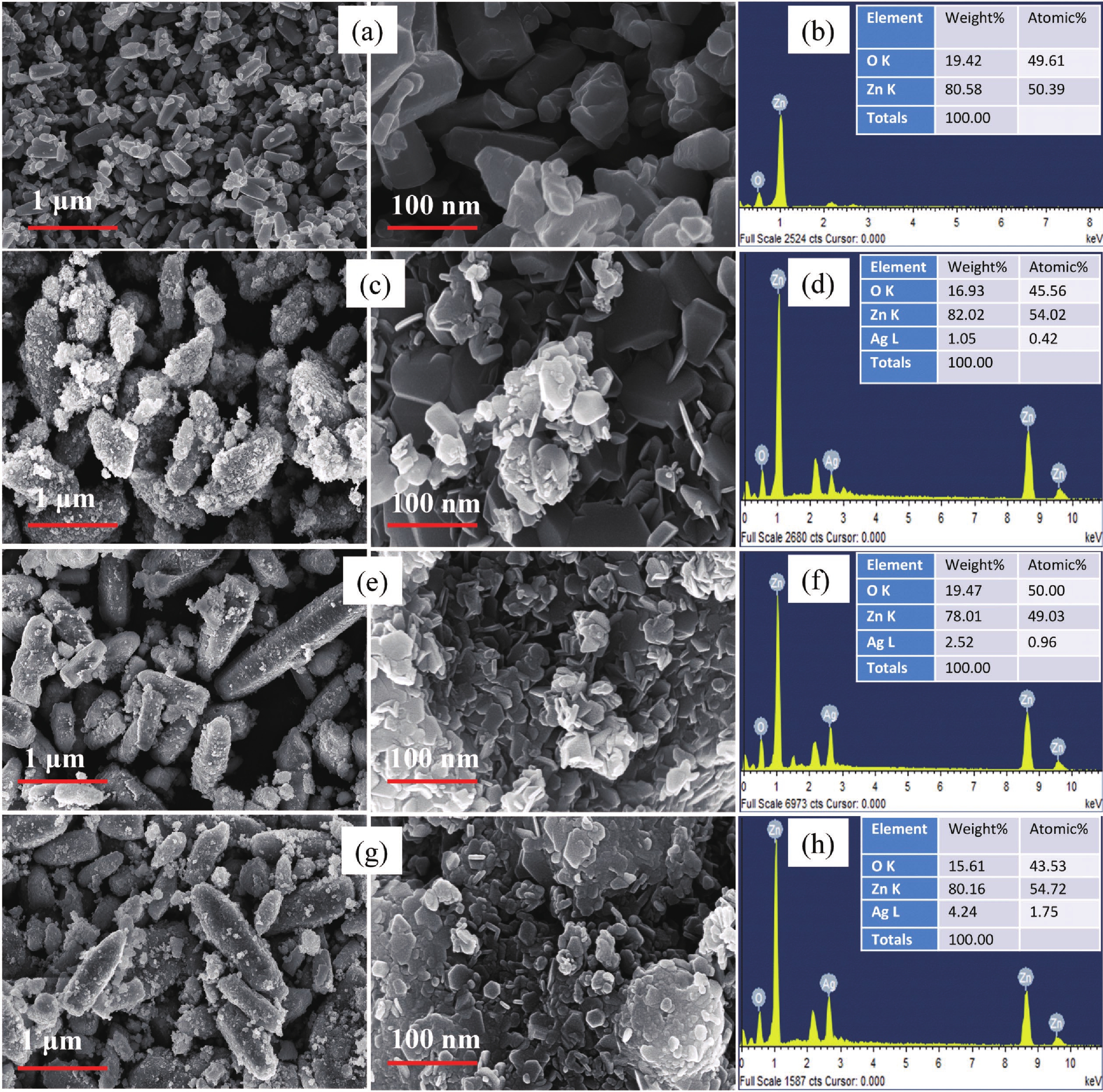
2022, 43(3): 032802 doi: 10.1088/1674-4926/43/3/032802

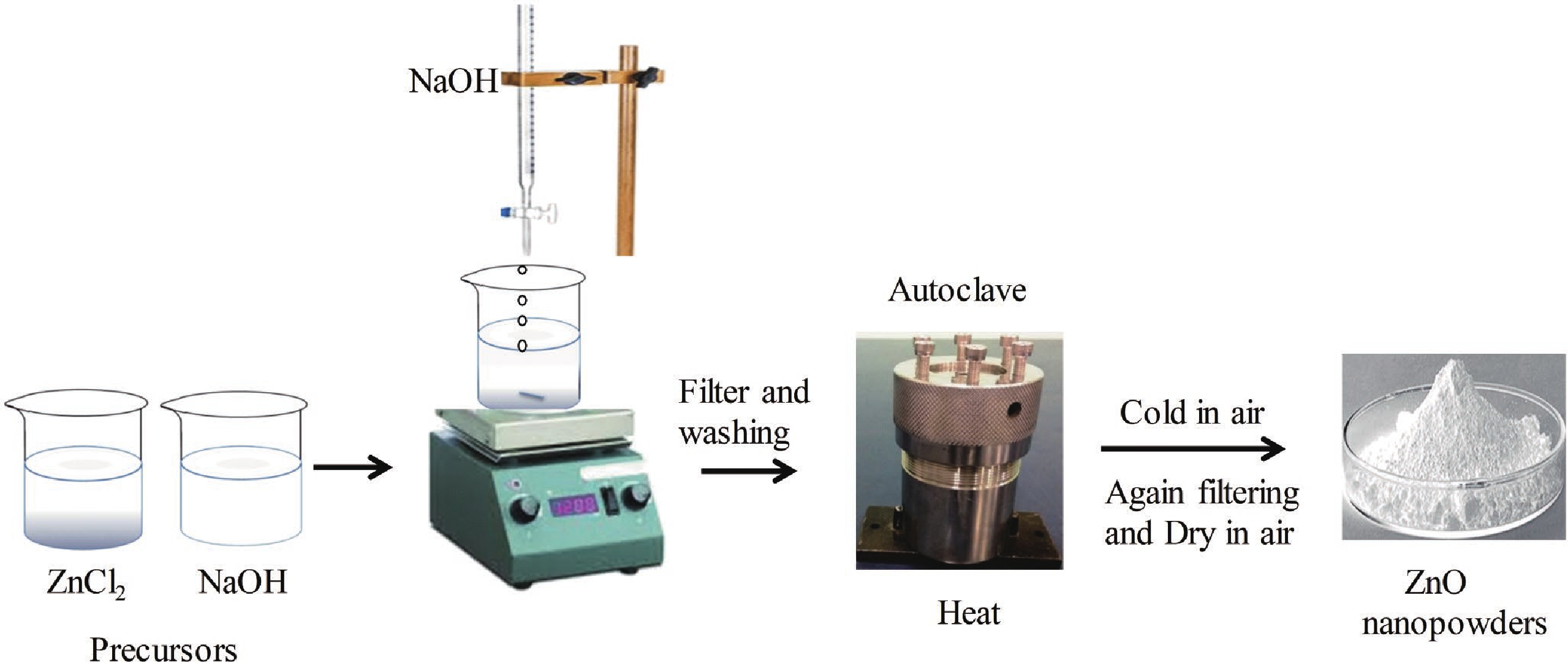
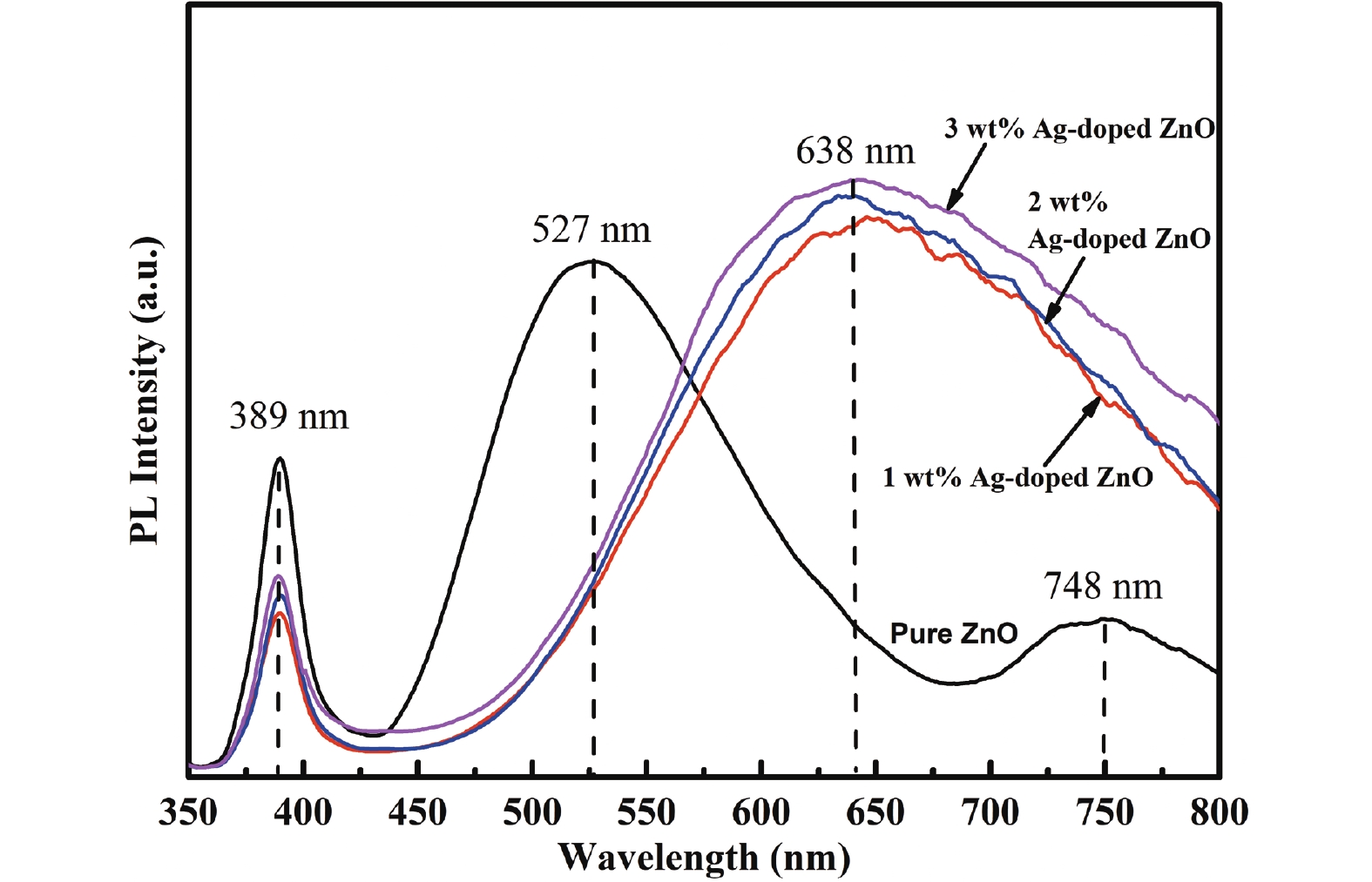
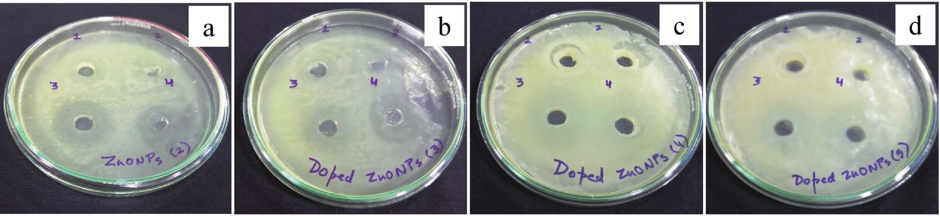
In the present work, zinc oxide (ZnO) and silver (Ag) doped ZnO nanostructures are synthesized using a hydrothermal method. Structural quality of the products is attested using X-ray diffraction, which confirms the hexagonal wurtzite structure of pure ZnO and Ag-doped ZnO nanostructures. XRD further confirms the crystallite orientation along the c-axis, (101) plane. The field emission scanning electron microscope study reveals the change in shape of the synthesized ZnO particles from hexagonal nanoparticles to needle-shaped nanostructures for 3 wt% Ag-doped ZnO. The optical band gaps and lattice strain of nanostructures is increased significantly with the increase of doping concentration of Ag in ZnO nanostructure. The antimicrobial activity of synthesized nanostructures has been evaluated against the gram-positive human pathogenic bacteria, Staphylococcus aureus via an agarose gel diffusion test. The maximum value of zone of inhibition (22 mm) is achieved for 3 wt% Ag-doped ZnO nanostructure and it clearly demonstrates the remarkable antibacterial activity.

J. Semicond.
2022, 43(3): 034101 doi: 10.1088/1674-4926/43/3/034101

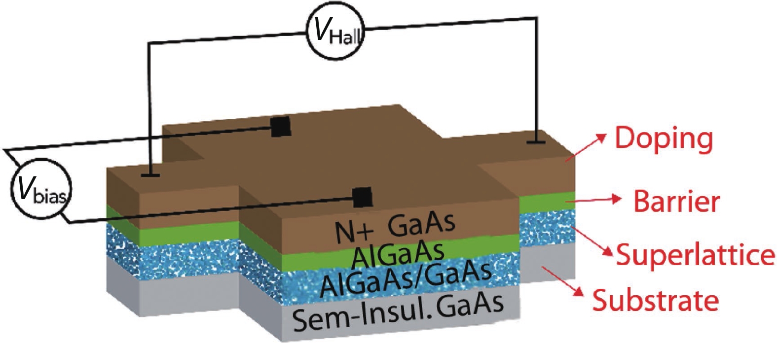
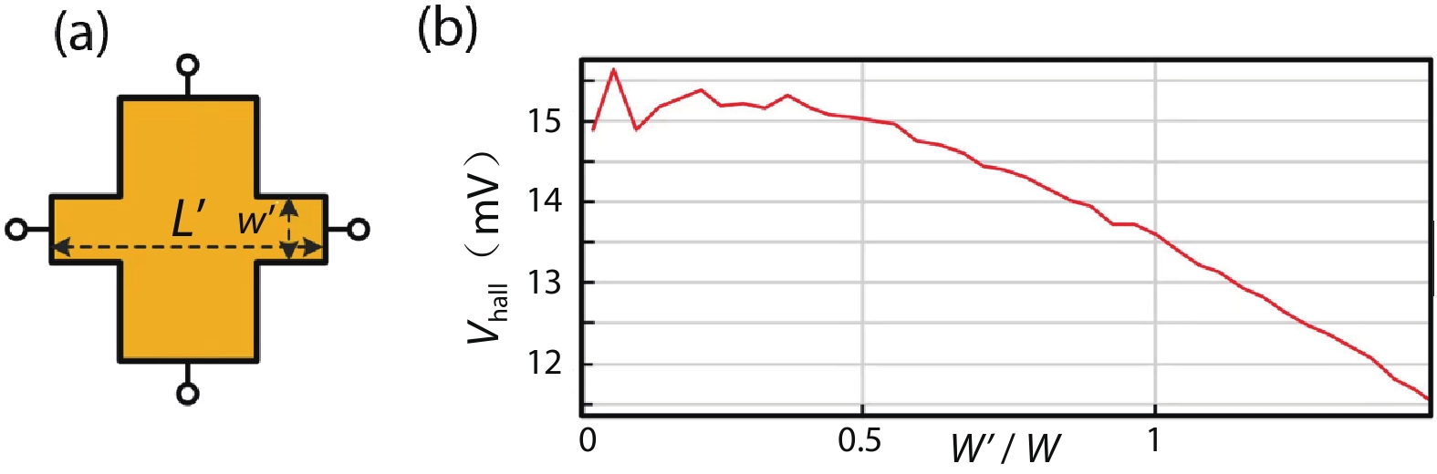
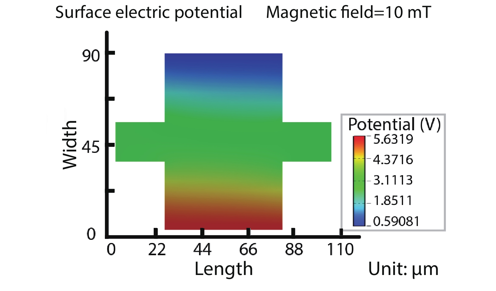
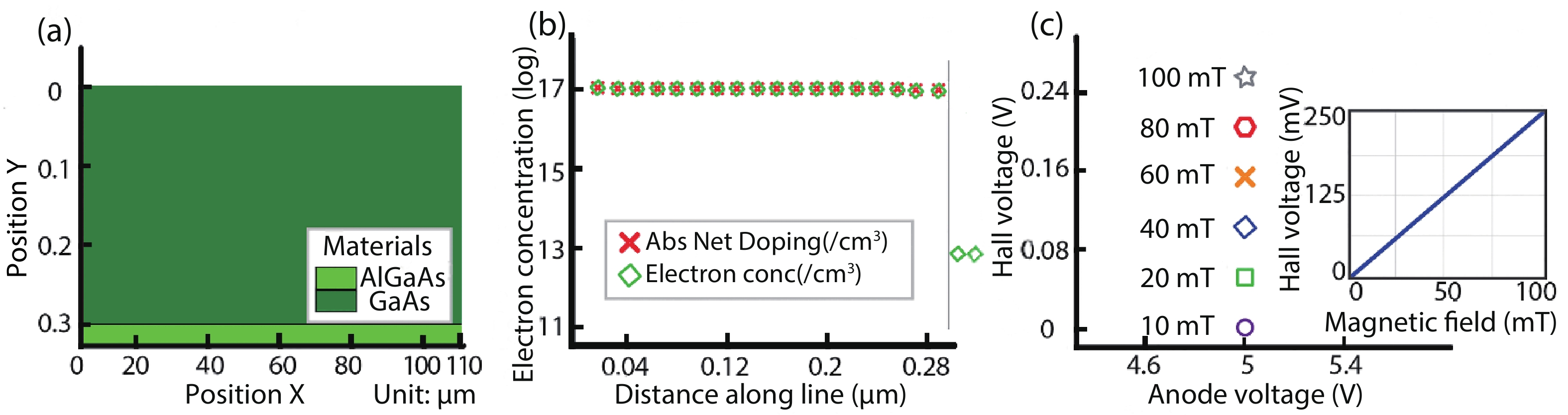
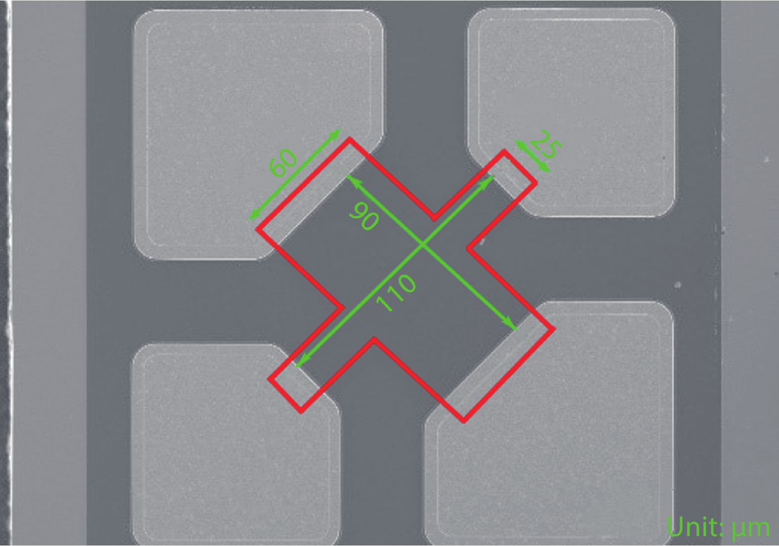
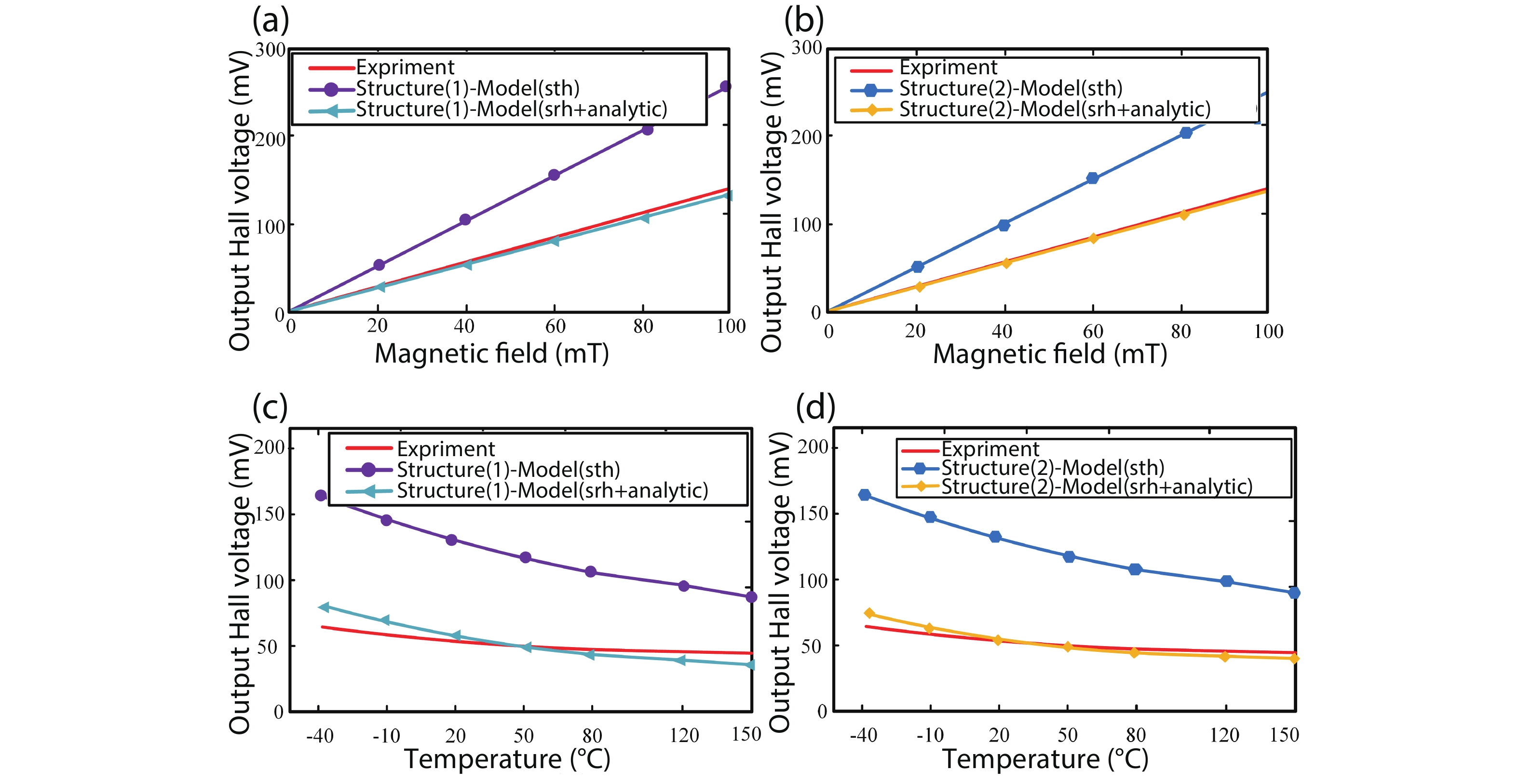
Silicon Hall-effect sensors have been widely used in industry and research fields due to their straightforward fabrication process and CMOS compatibility. However, as their material property limitations, technicians usually implement complex CMOS circuits to improve the sensors’ performance including temperature drift and offset compensation for fitting tough situation, but it is no doubt that it increases the design complexity and the sensor area. Gallium arsenide (GaAs) is a superior material of Hall-effect device because of its large mobility and stable temperature characteristics. Concerning there is no specified modelling of GaAs Hall-effect device, this paper investigated its modelling by using finite element method (FEM) software Silvaco TCAD® to help and guide GaAs Hall-effect device fabrication. The modeled sensor has been fabricated and its experimental results are in agreement with the simulation results. Comparing to our previous silicon Hall-effect sensor, the GaAs Hall-effect sensor demonstrates potential and reliable benchmark for the future Hall magnetic sensor developments.
J. Semicond.
2022, 43(3): 034102 doi: 10.1088/1674-4926/43/3/034102
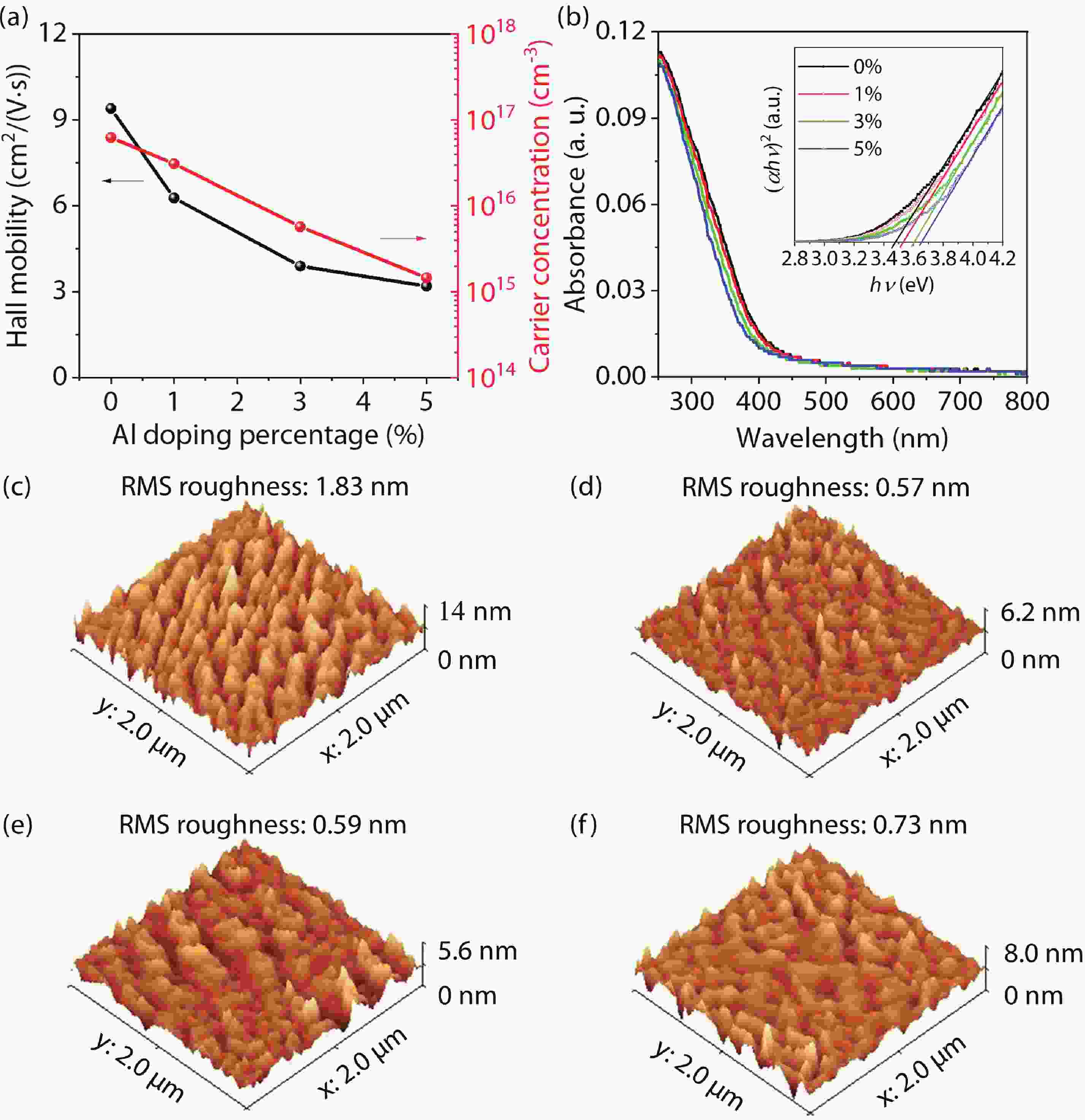
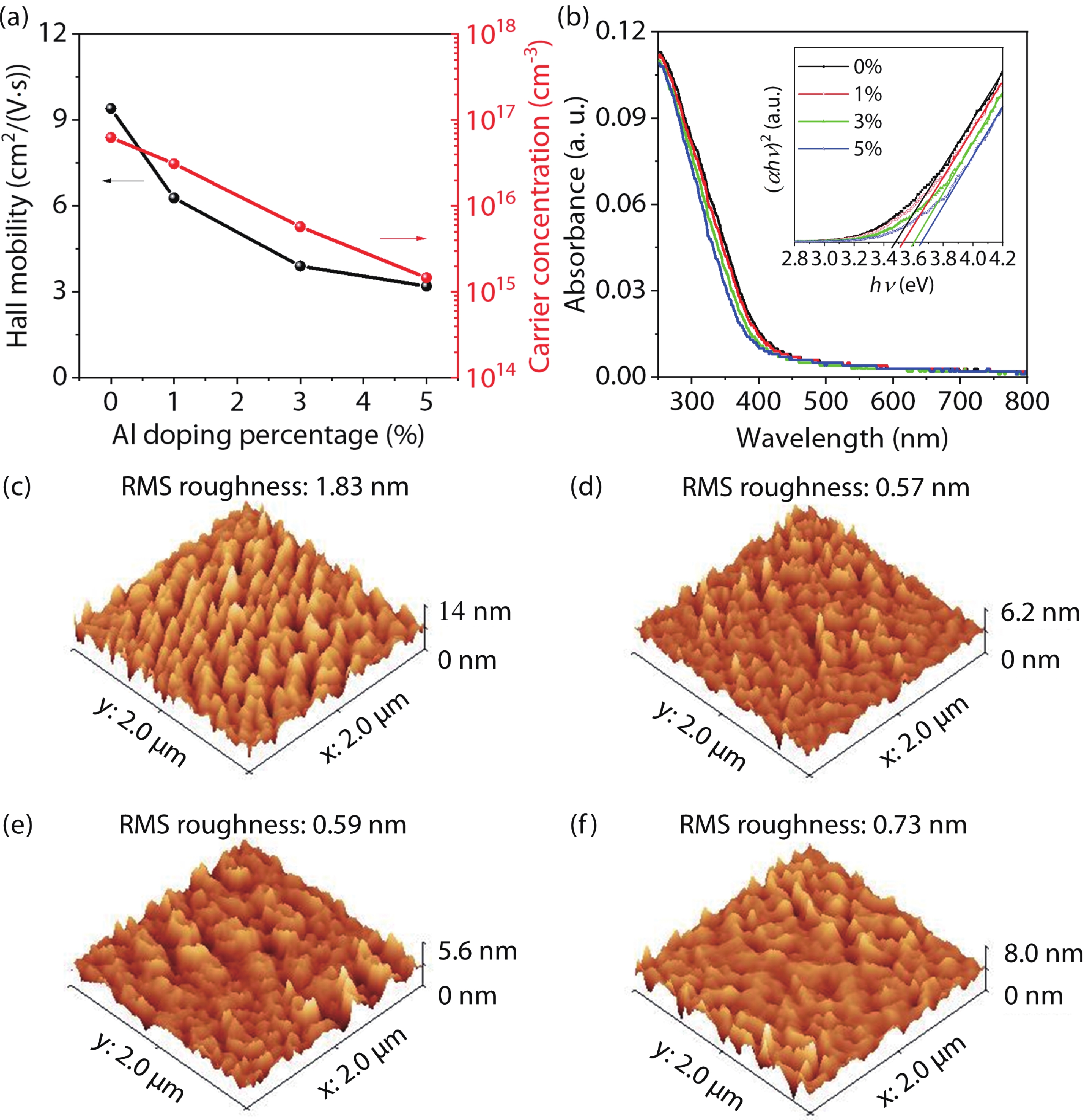
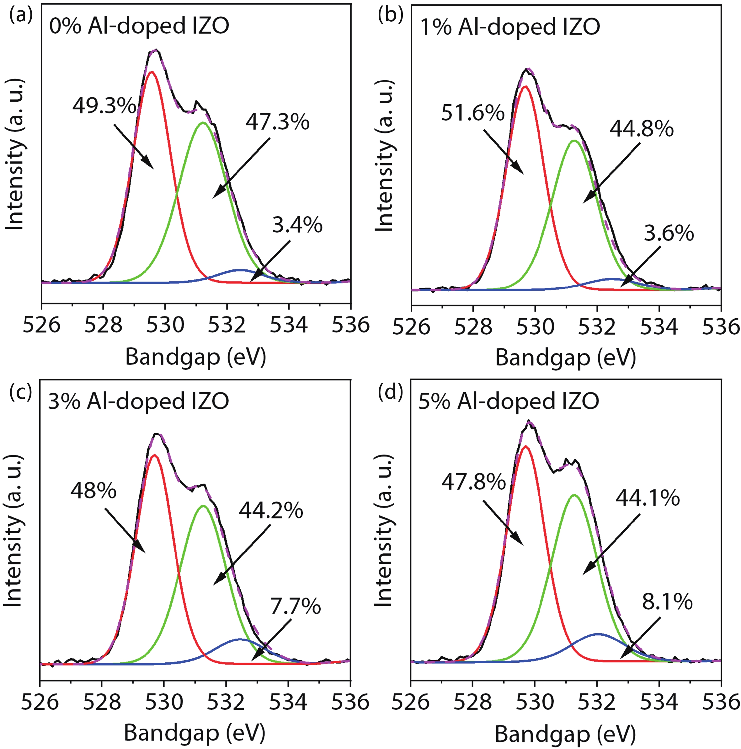
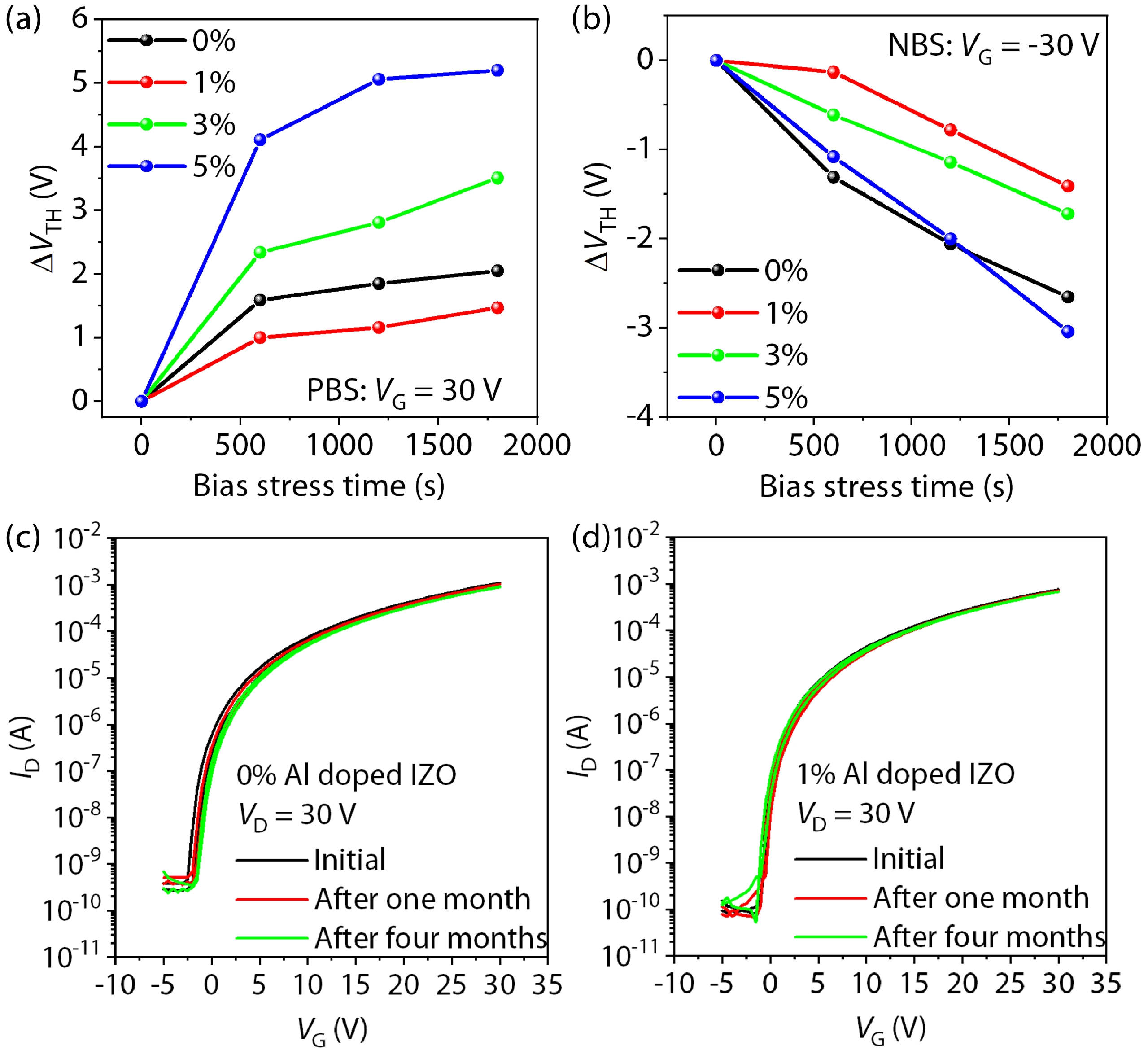
Solution-processed oxide semiconductors have been considered as a potential alternative to vacuum-based ones in printable electronics. However, despite spin-coated InZnO (IZO) thin-film transistors (TFTs) have shown a relatively high mobility, the lack of carrier suppressor and the high sensitivity to oxygen and water molecules in ambient air make them potentially suffer issues of poor stability. In this work, Al is used as the third cation doping element to study the effects on the electrical, optoelectronic, and physical properties of IZO TFTs. A hydrophobic self-assembled monolayer called octadecyltrimethoxysilane is introduced as the surface passivation layer, aiming to reduce the effects from air and understand the importance of top surface conditions in solution-processed, ultra-thin oxide TFTs. Owing to the reduced trap states within the film and at the top surface enabled by the doping and passivation, the optimized TFTs show an increased current on/off ratio, a reduced drain current hysteresis, and a significantly enhanced bias stress stability, compared with the untreated ones. By combining with high-capacitance AlOx, TFTs with a low operating voltage of 1.5 V, a current on/off ratio of > 104 and a mobility of 4.6 cm2/(V·s) are demonstrated, suggesting the promising features for future low-cost, low-power electronics.