Issue Browser
Volume 44, Issue 6,
Jun 2023


J. Semicond.
2023, 44(6): 061801 doi: 10.1088/1674-4926/44/6/061801
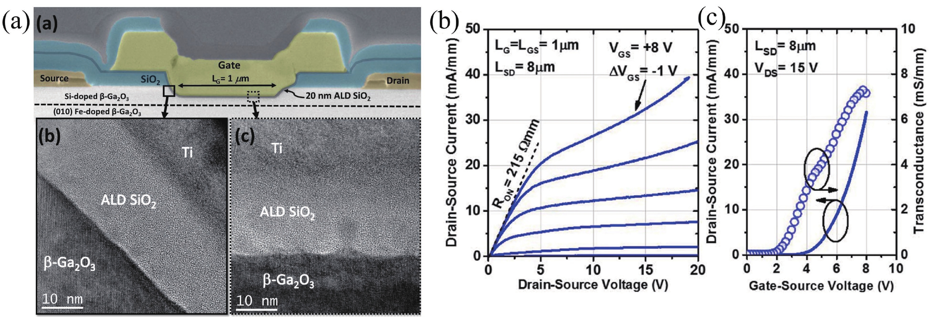
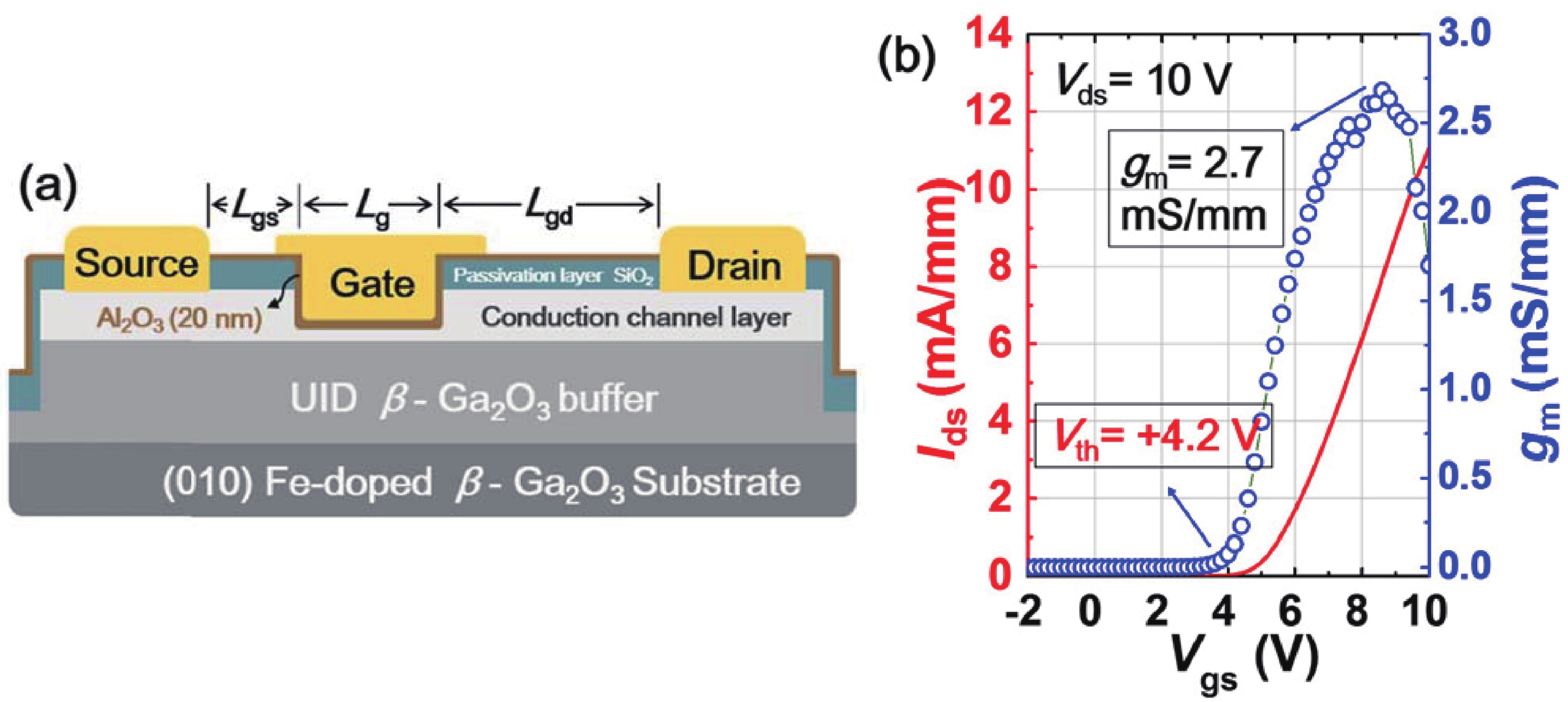
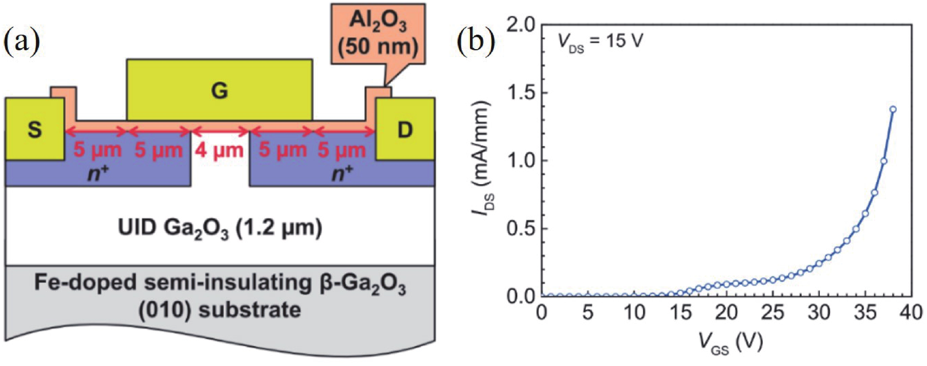
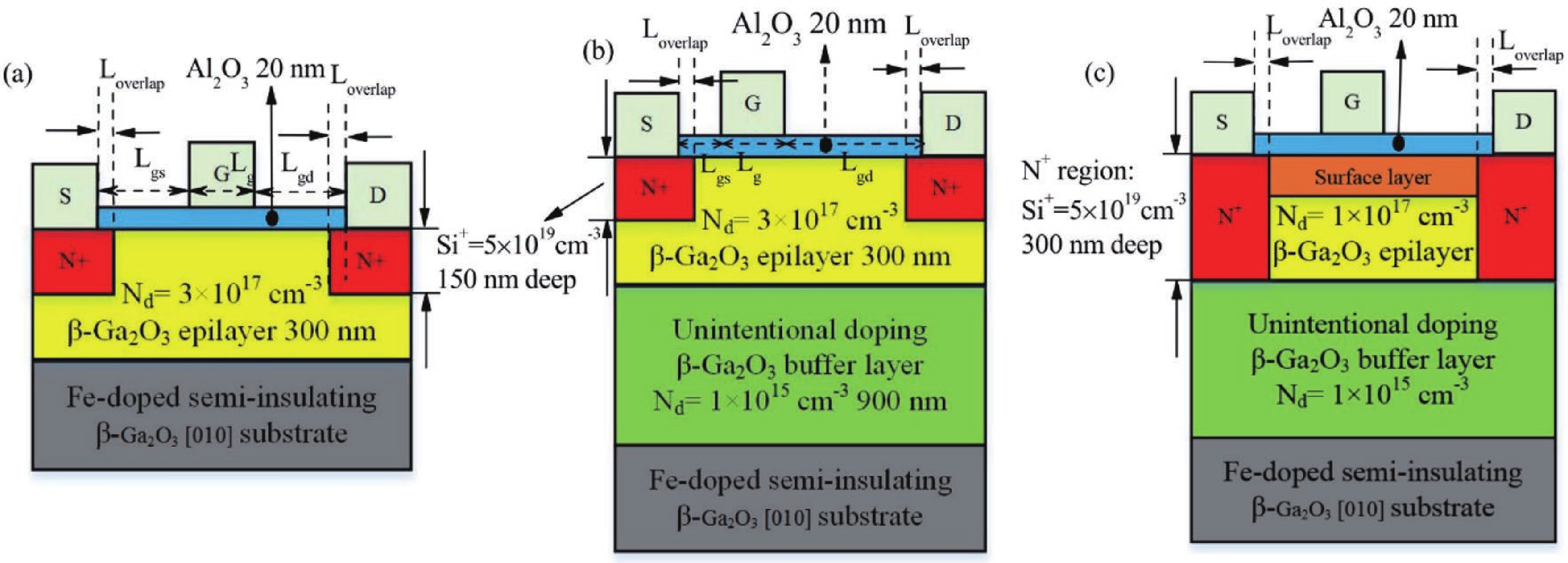
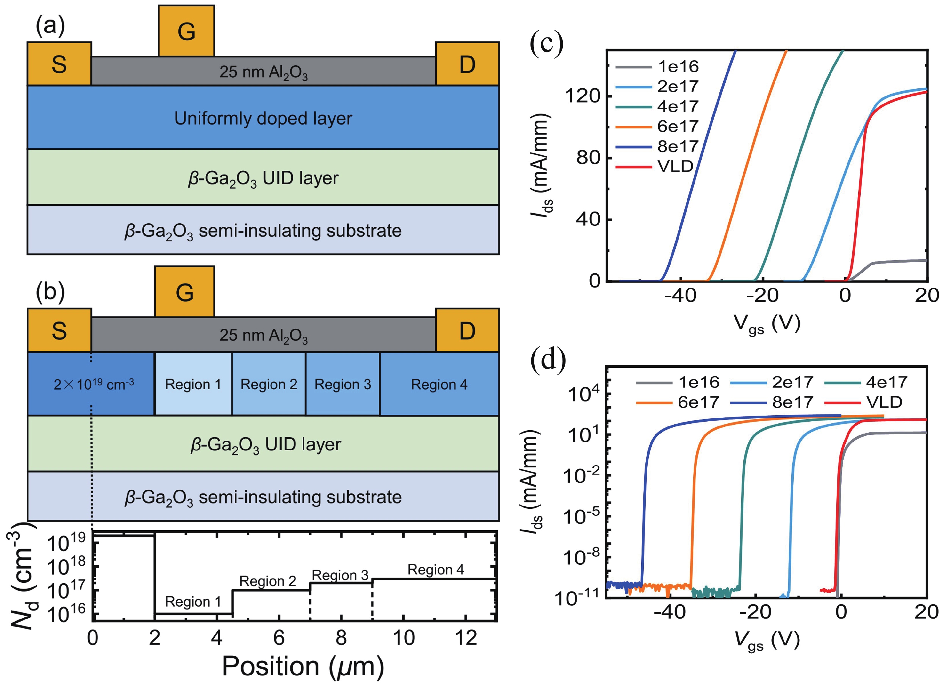
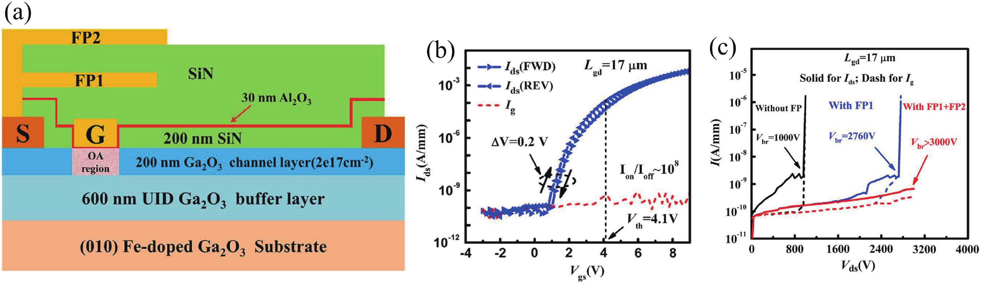
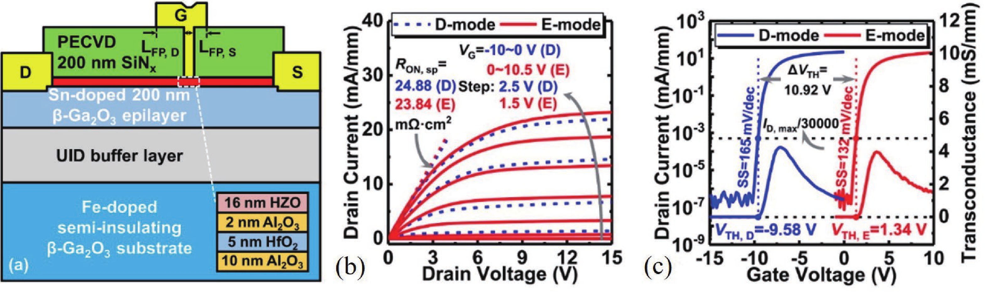
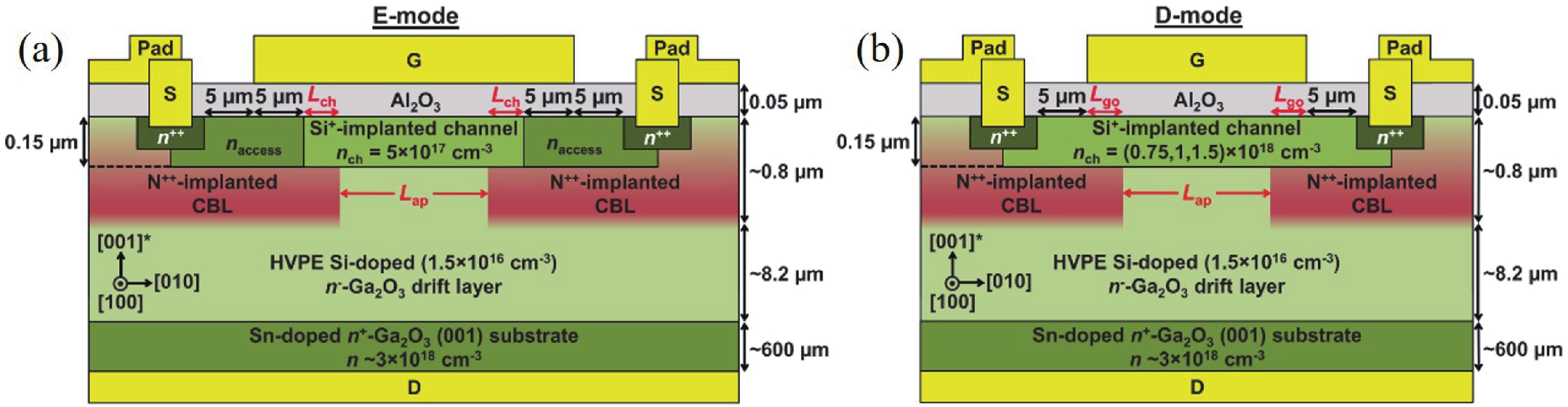
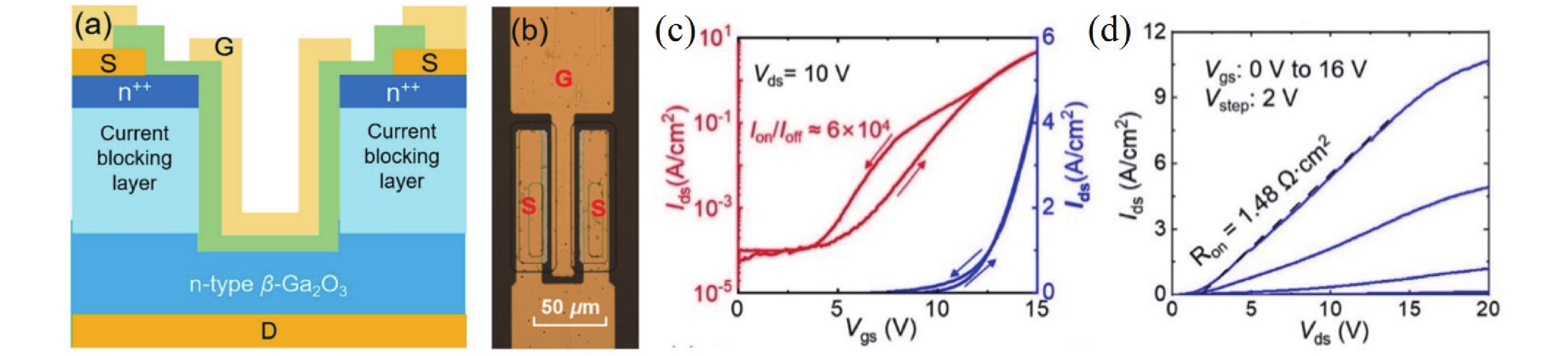
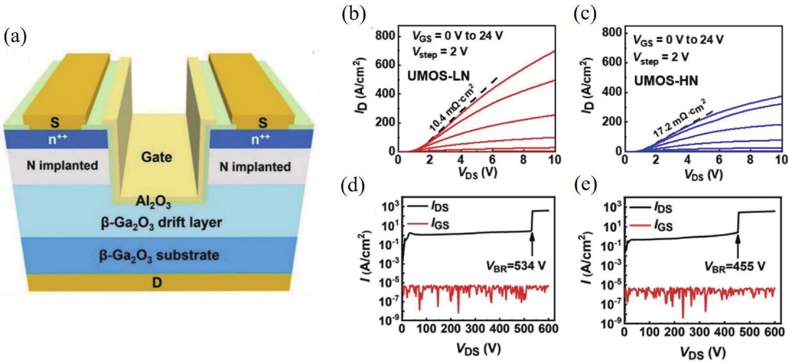
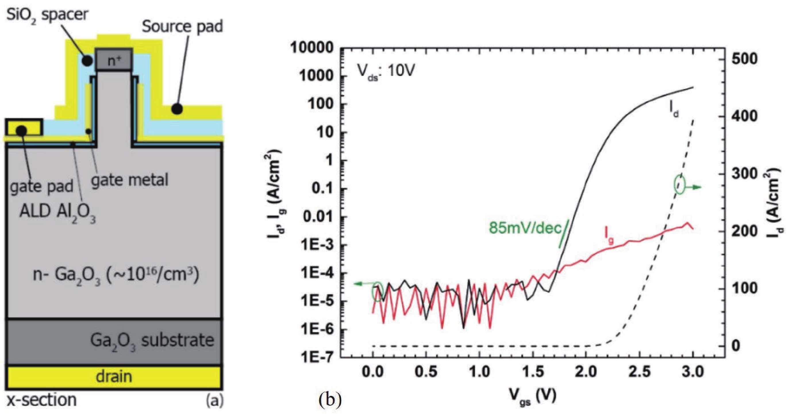
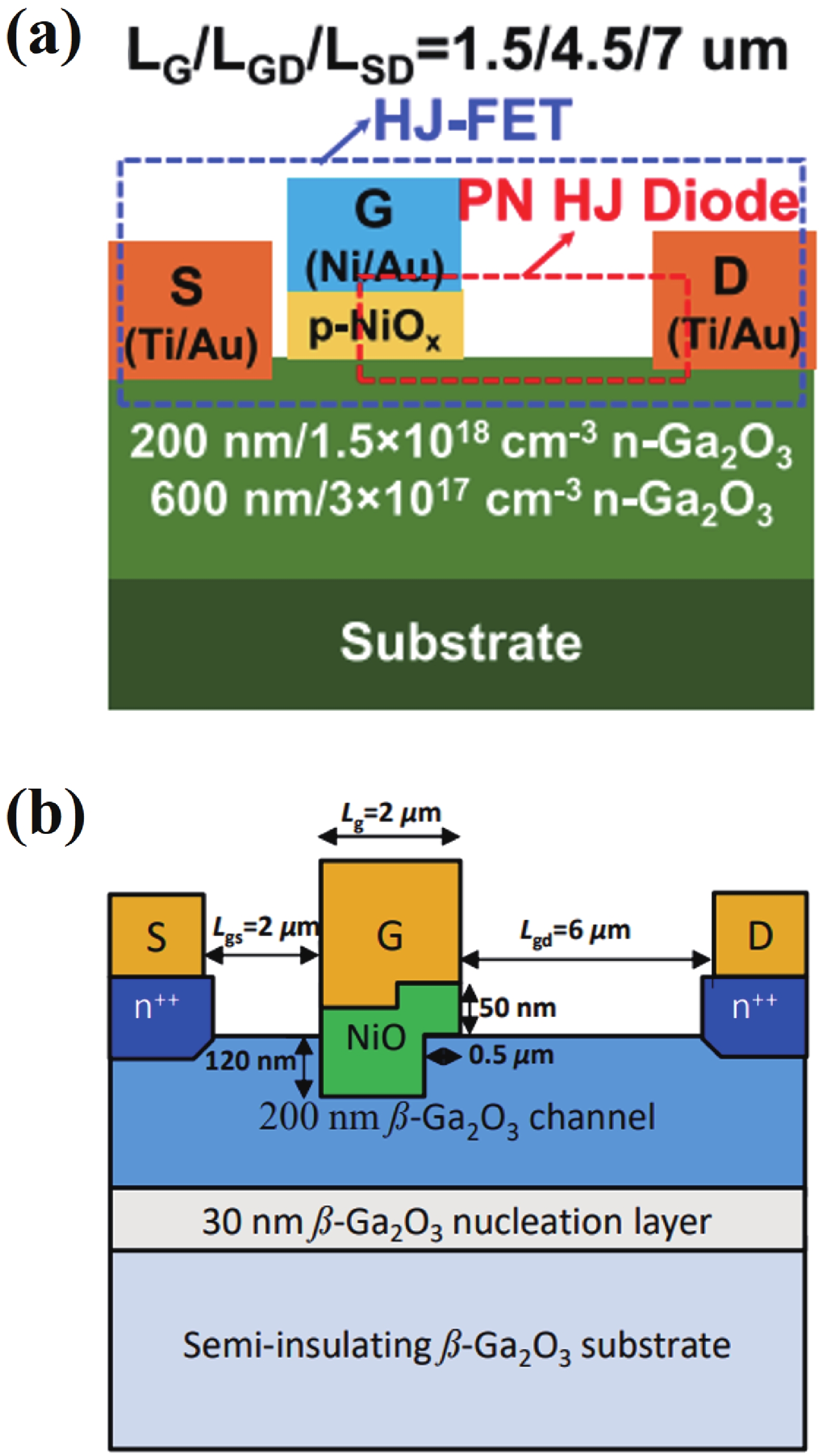
Power electronic devices are of great importance in modern society. After decades of development, Si power devices have approached their material limits with only incremental improvements and large conversion losses. As the demand for electronic components with high efficiency dramatically increasing, new materials are needed for power device fabrication. Beta-phase gallium oxide, an ultra-wide bandgap semiconductor, has been considered as a promising candidate, and various β-Ga2O3 power devices with high breakdown voltages have been demonstrated. However, the realization of enhancement-mode (E-mode) β-Ga2O3 field-effect transistors (FETs) is still challenging, which is a critical problem for a myriad of power electronic applications. Recently, researchers have made some progress on E-mode β-Ga2O3 FETs via various methods, and several novel structures have been fabricated. This article gives a review of the material growth, devices and properties of these E-mode β-Ga2O3 FETs. The key challenges and future directions in E-mode β-Ga2O3 FETs are also discussed.

J. Semicond.
2023, 44(6): 061802 doi: 10.1088/1674-4926/44/6/061802
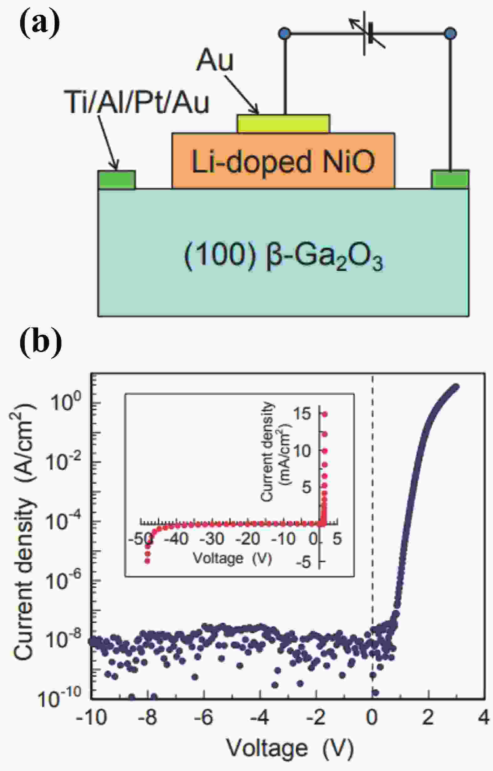
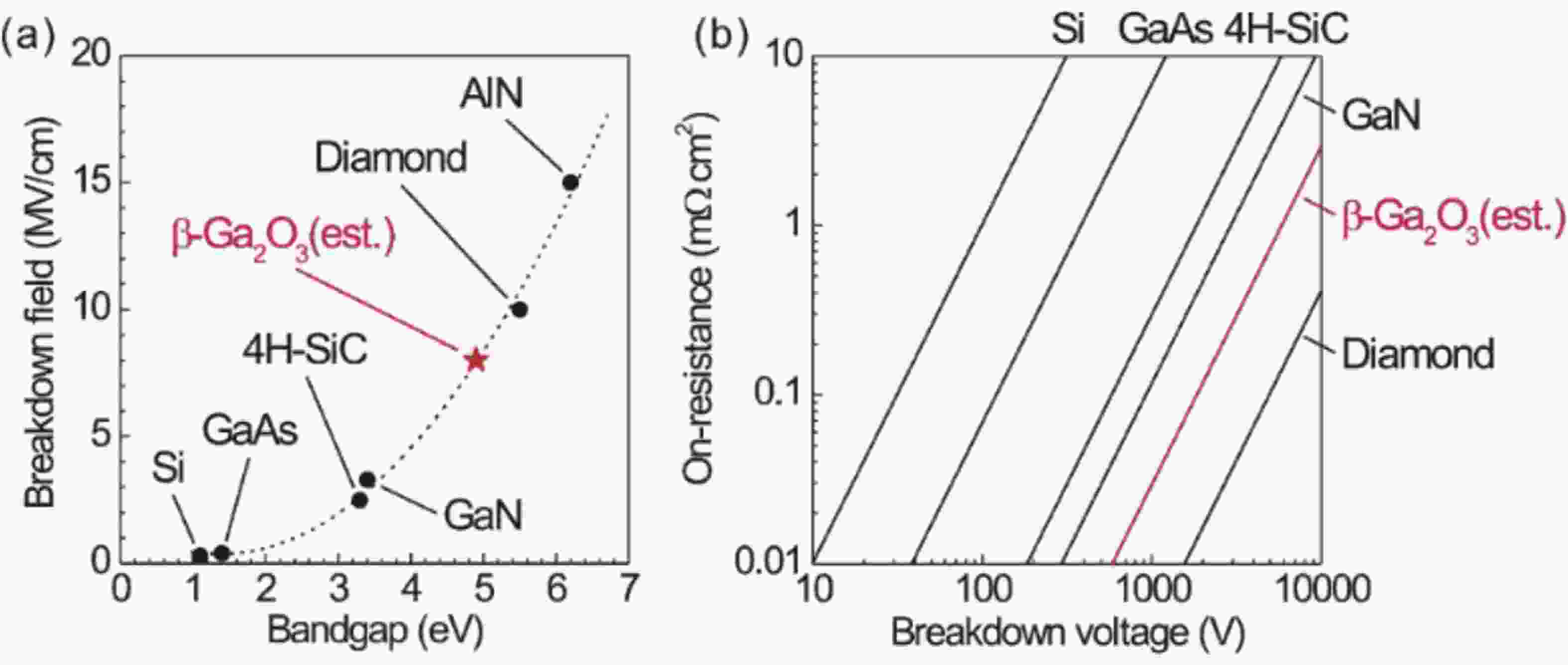
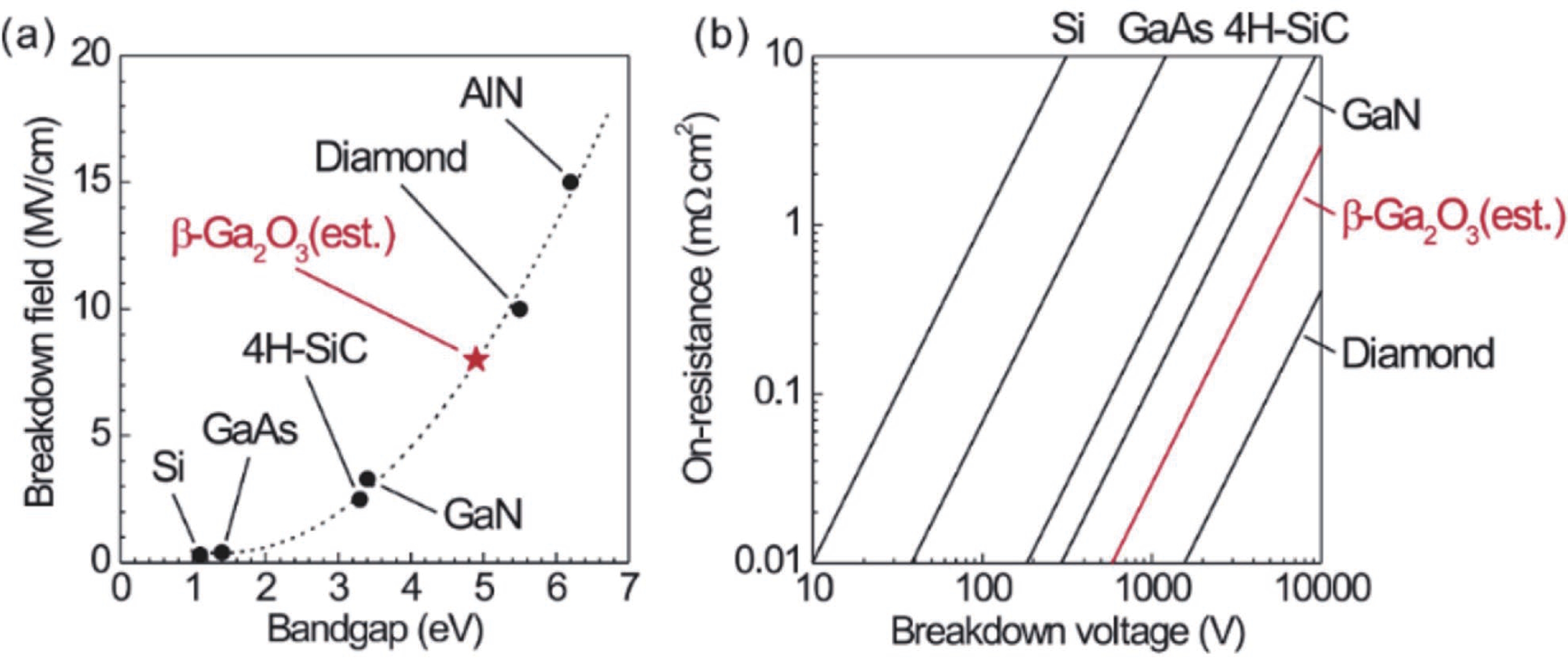
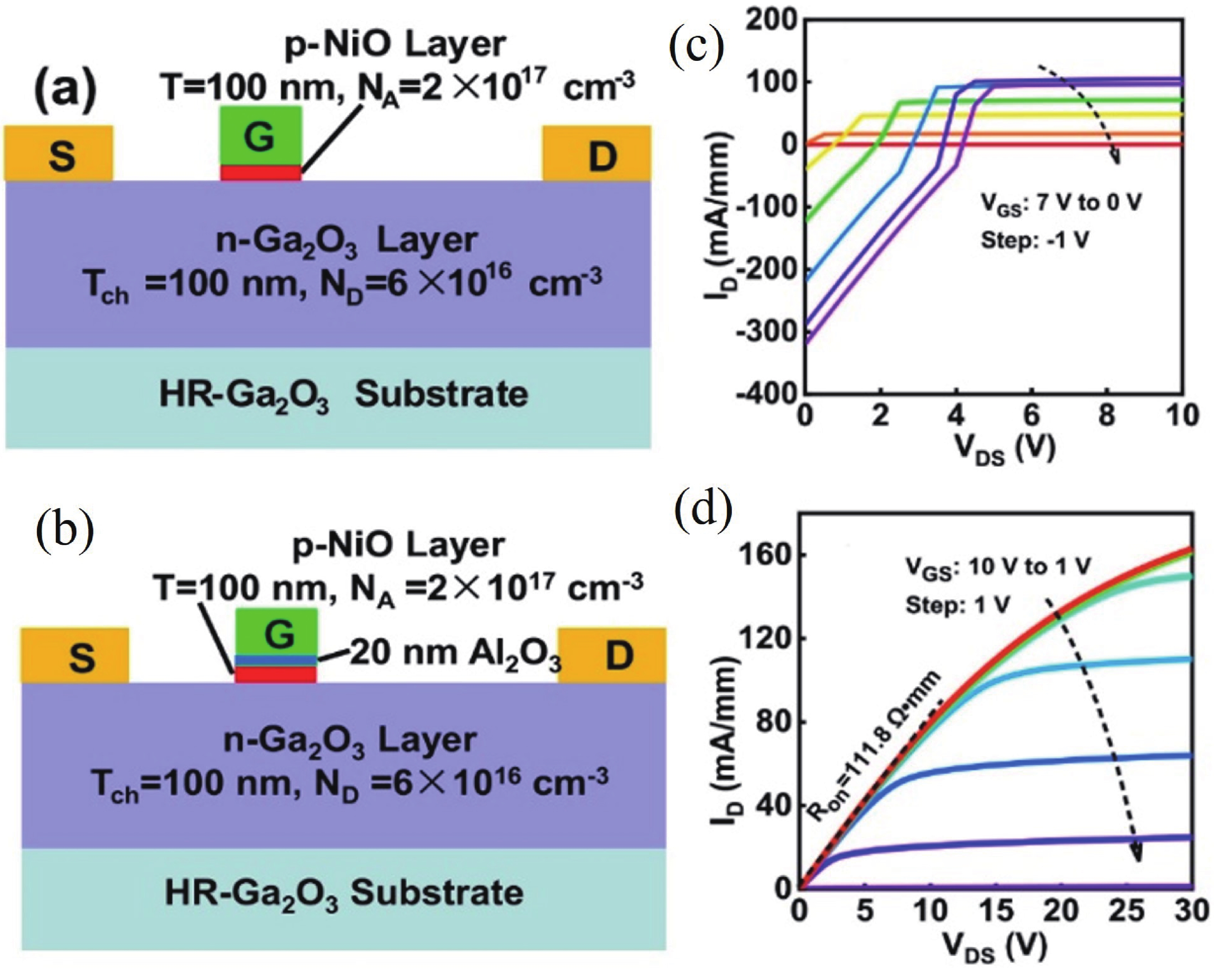
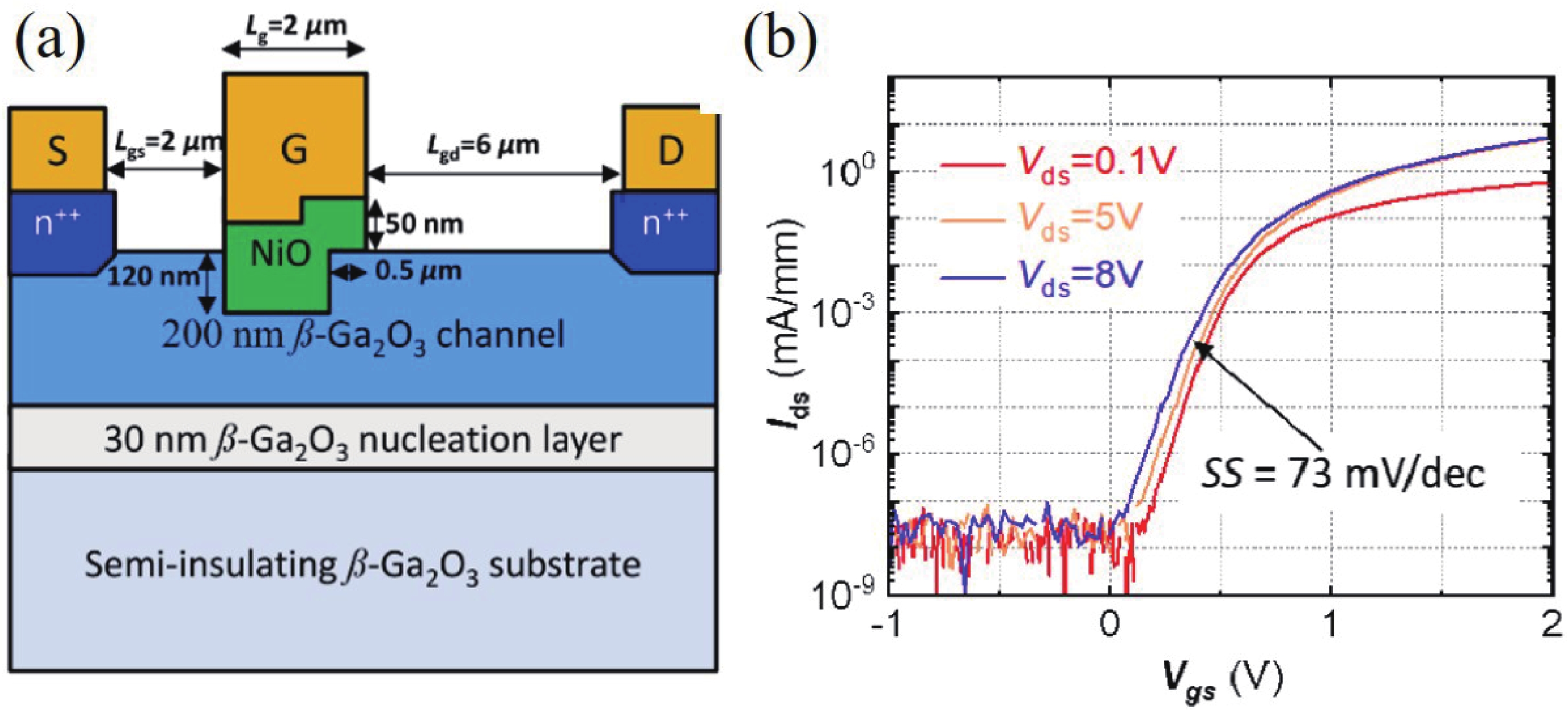
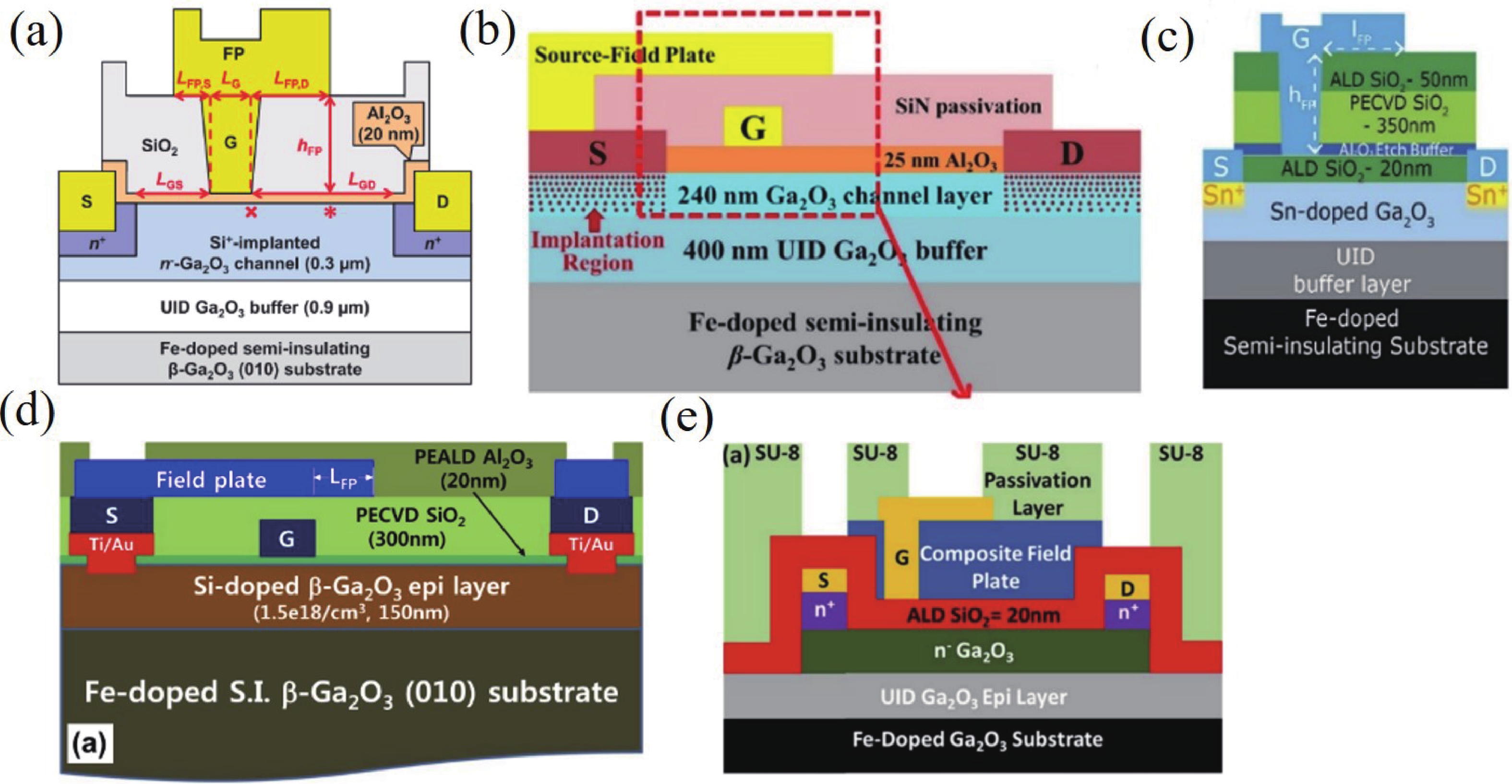
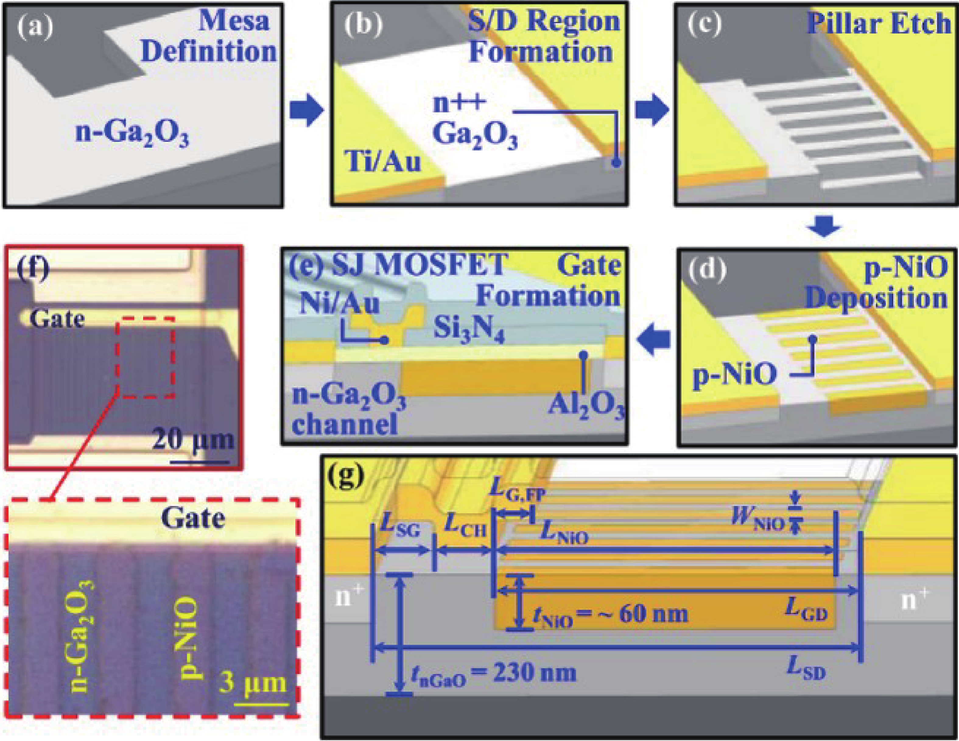
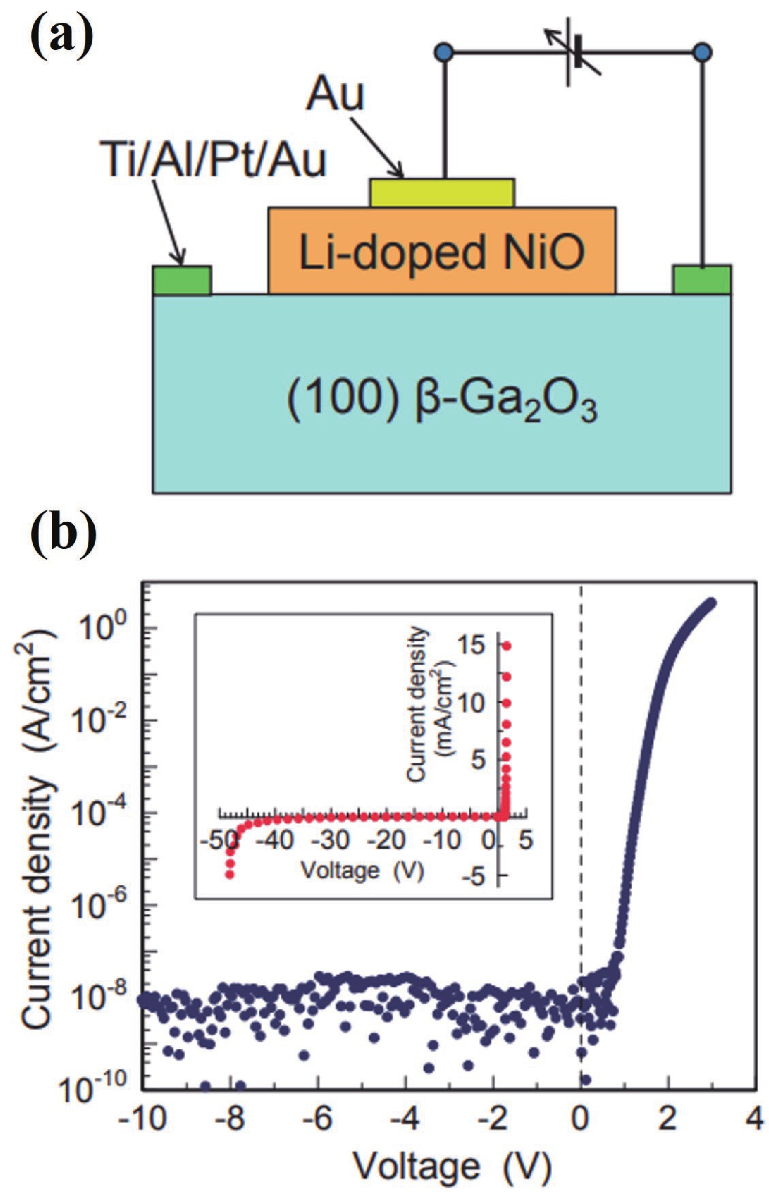
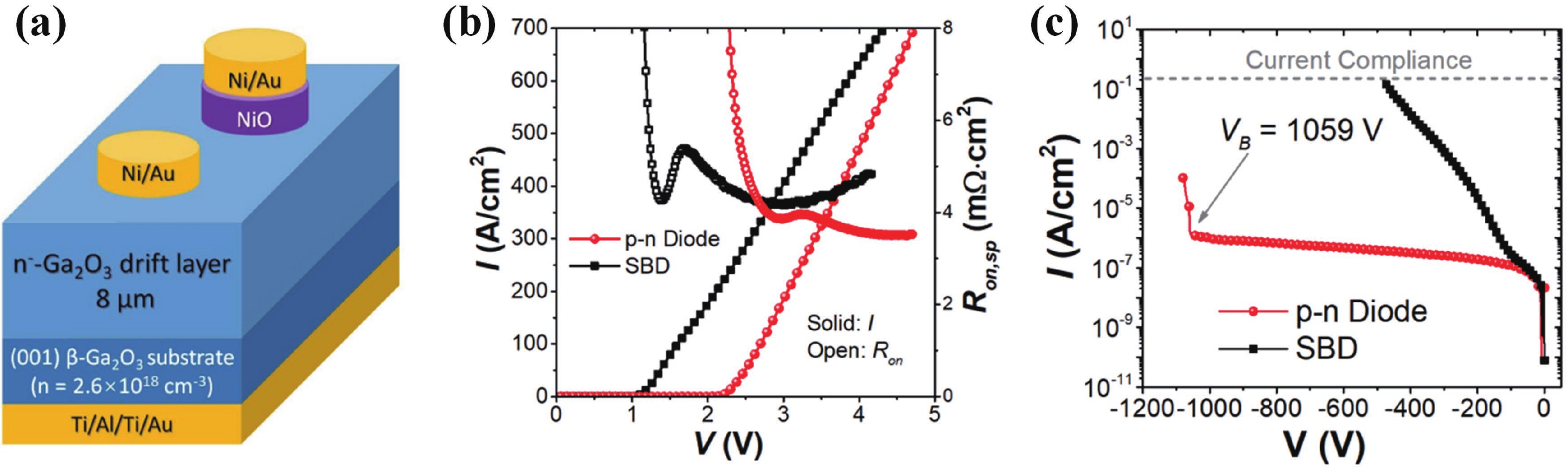
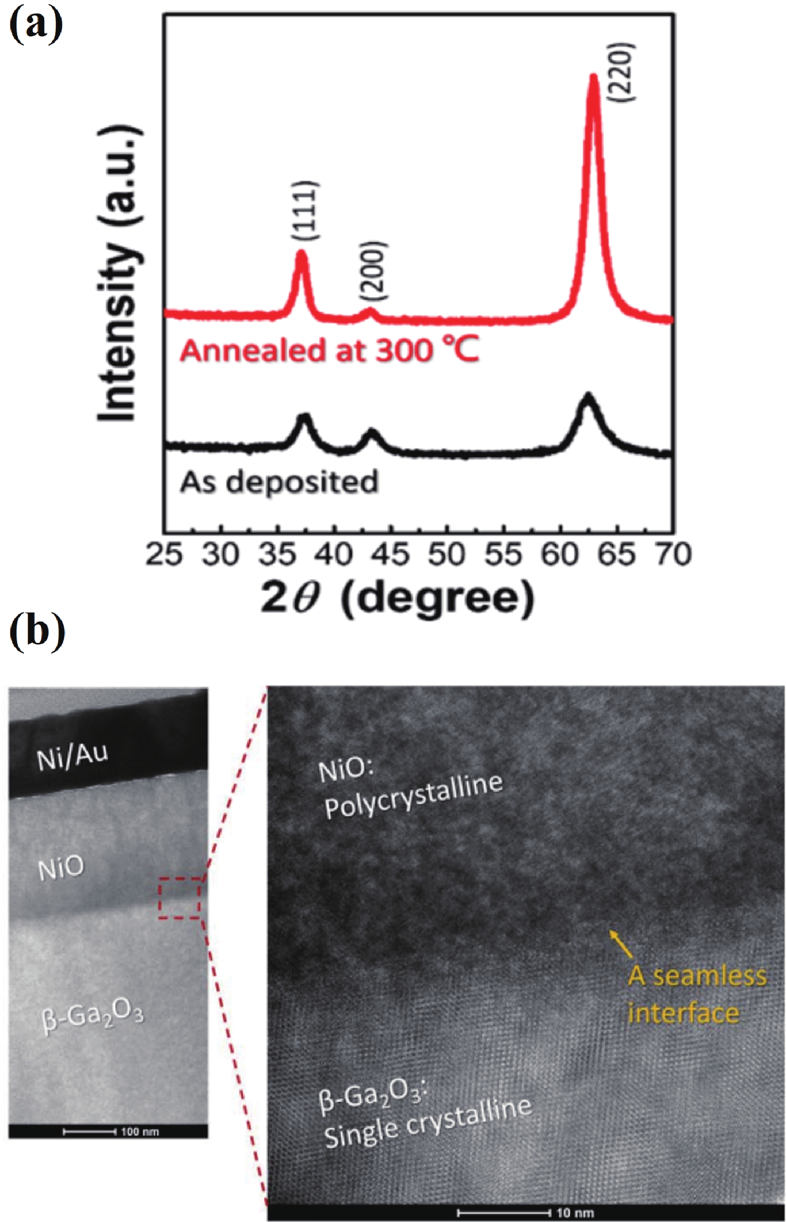
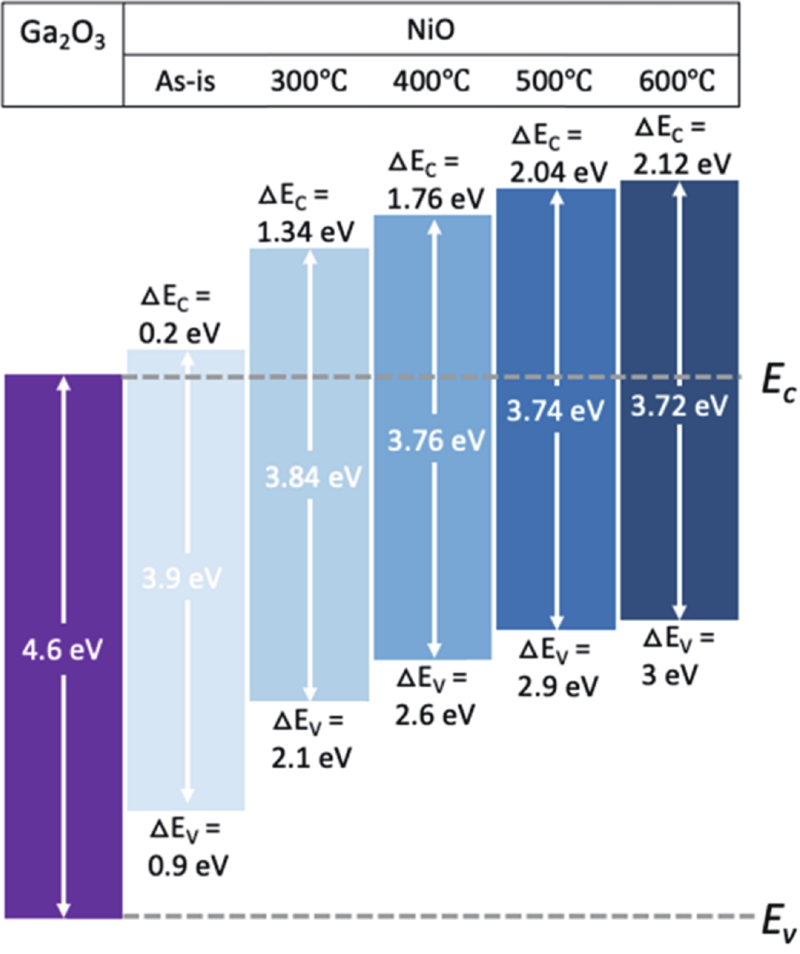
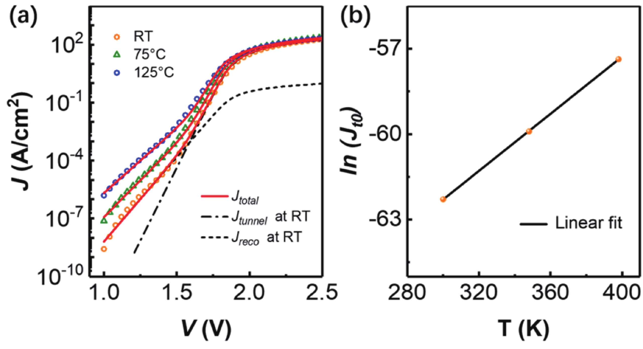
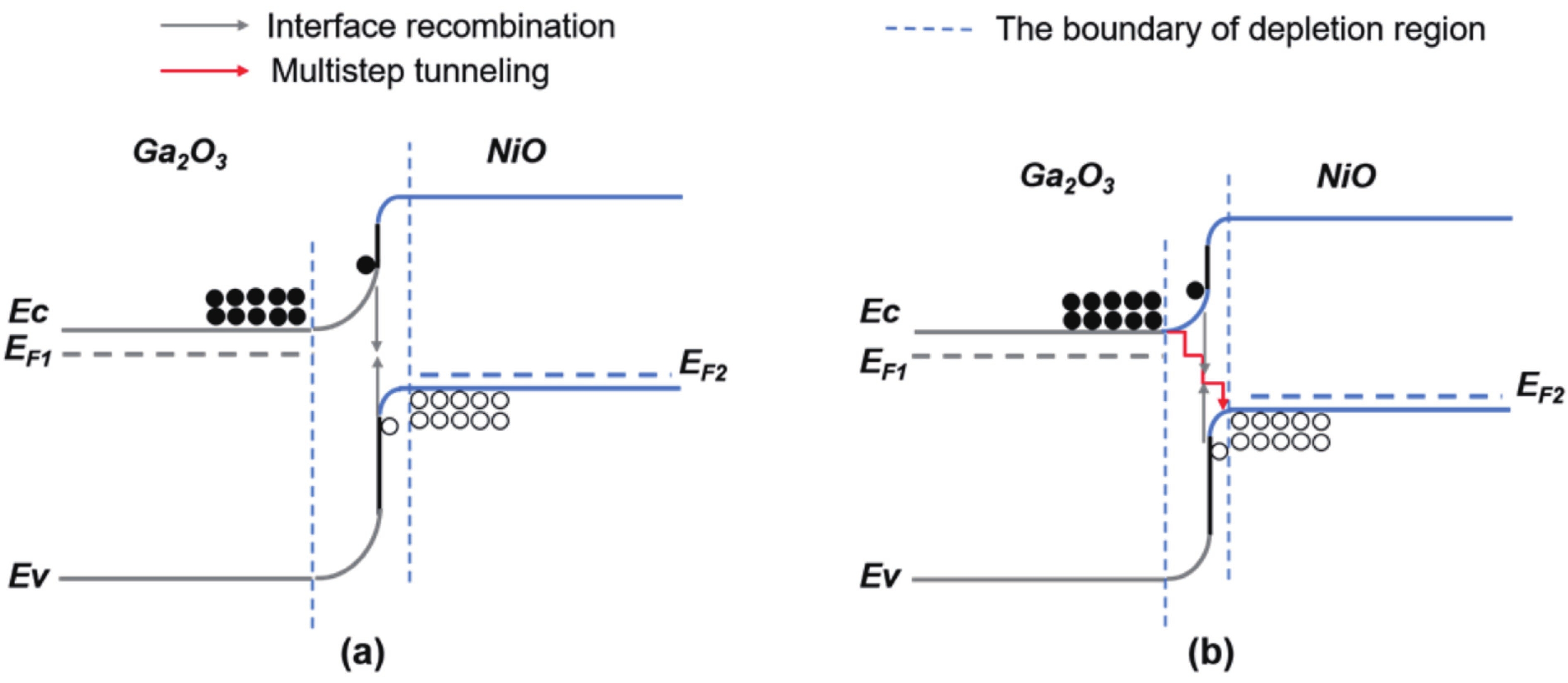
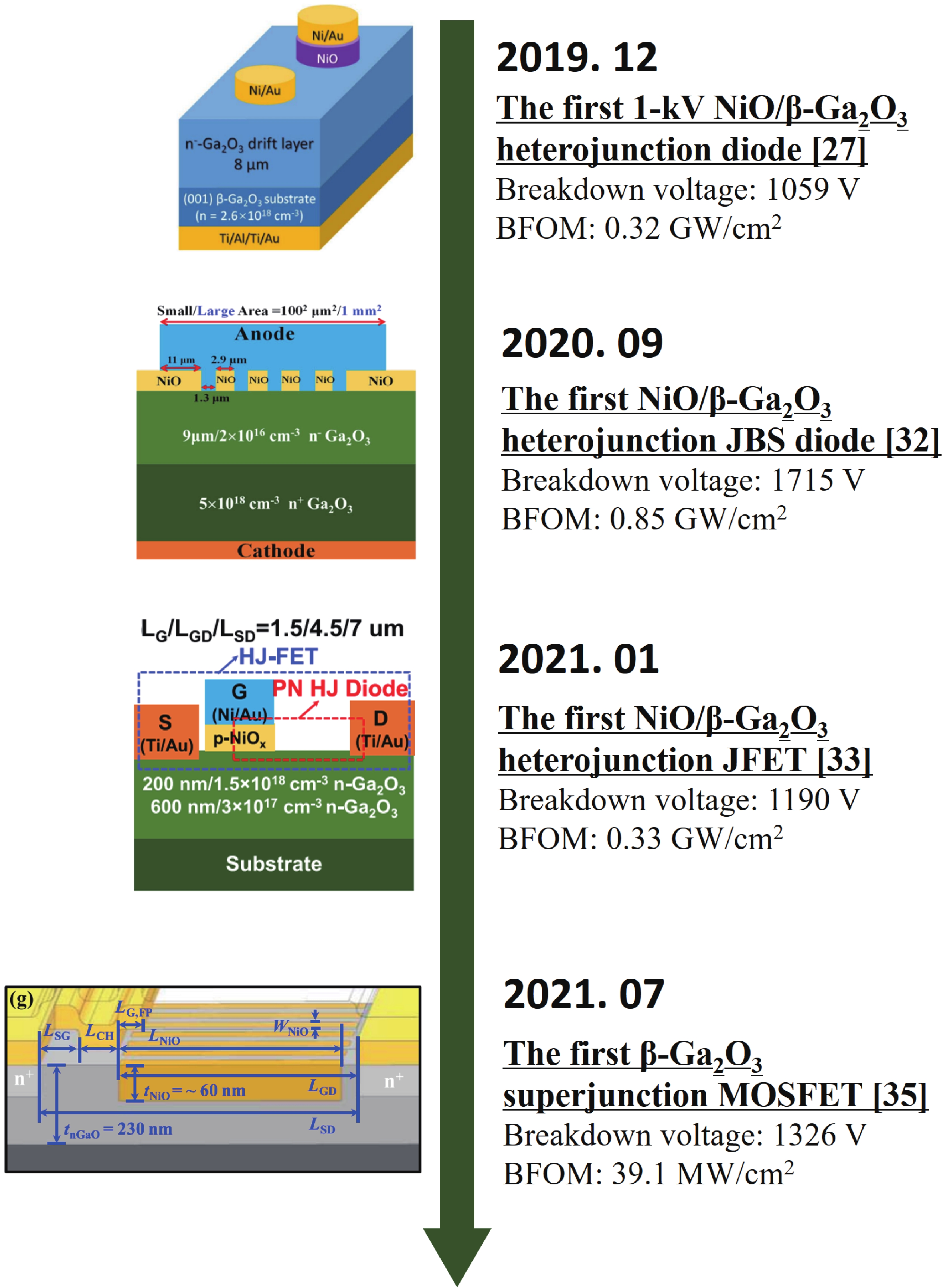
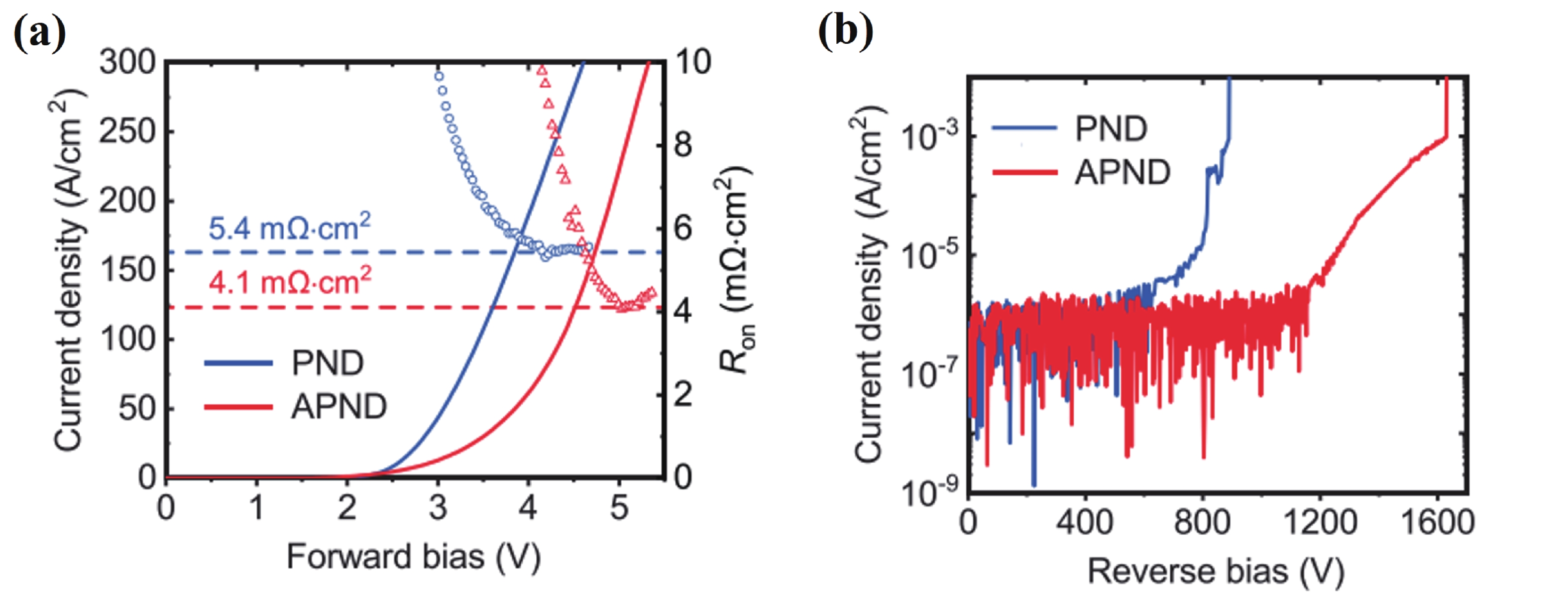
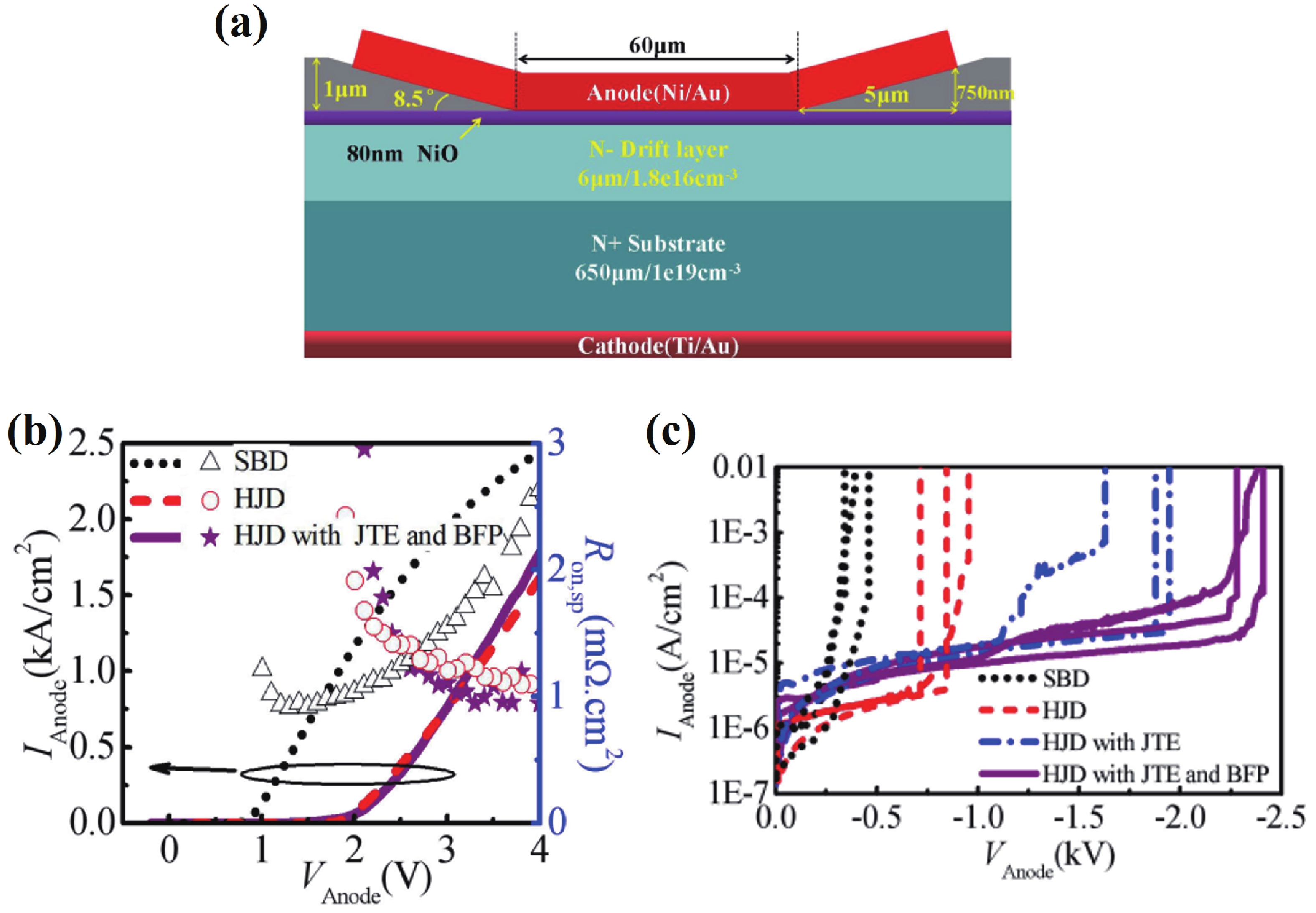
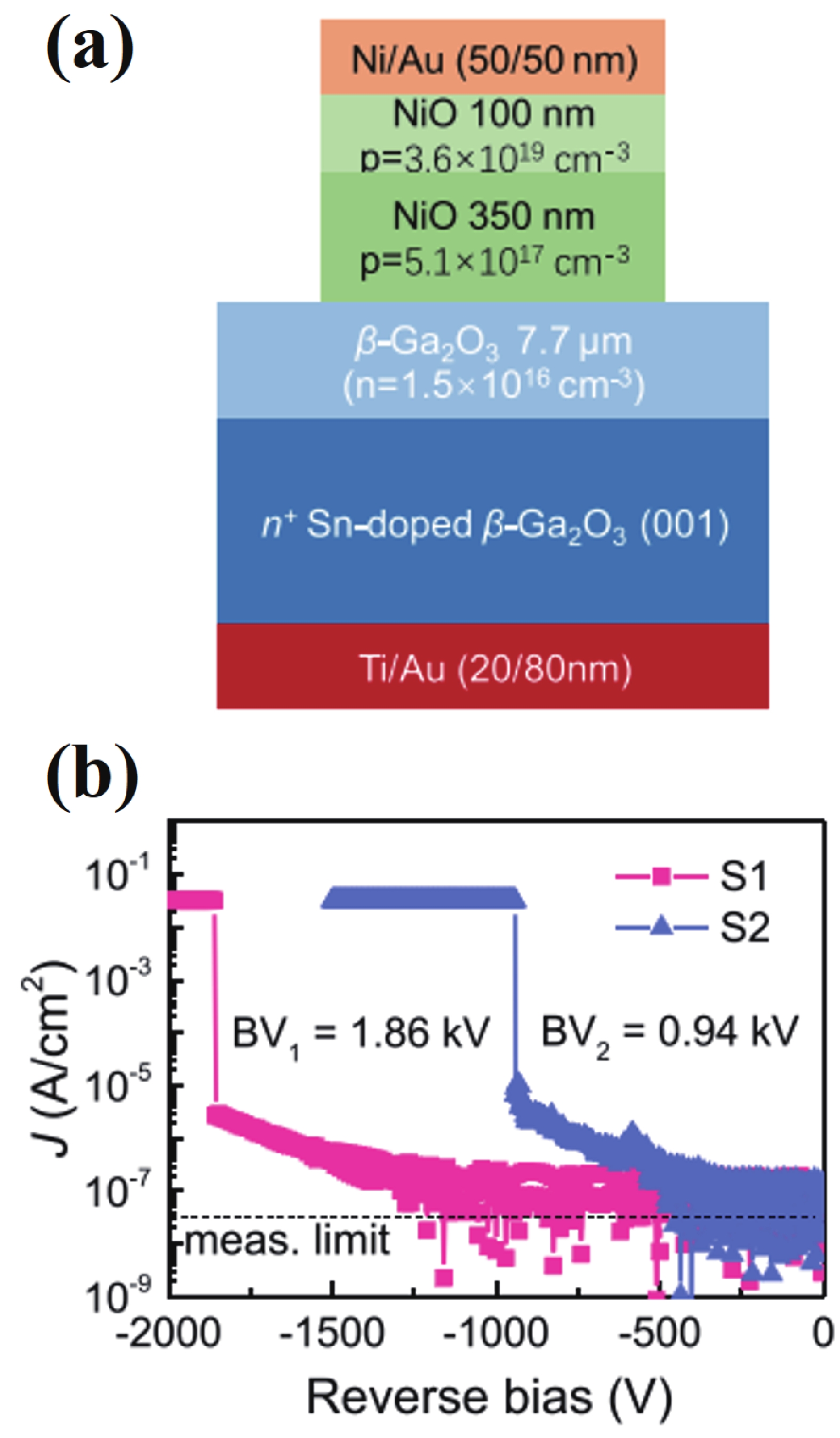
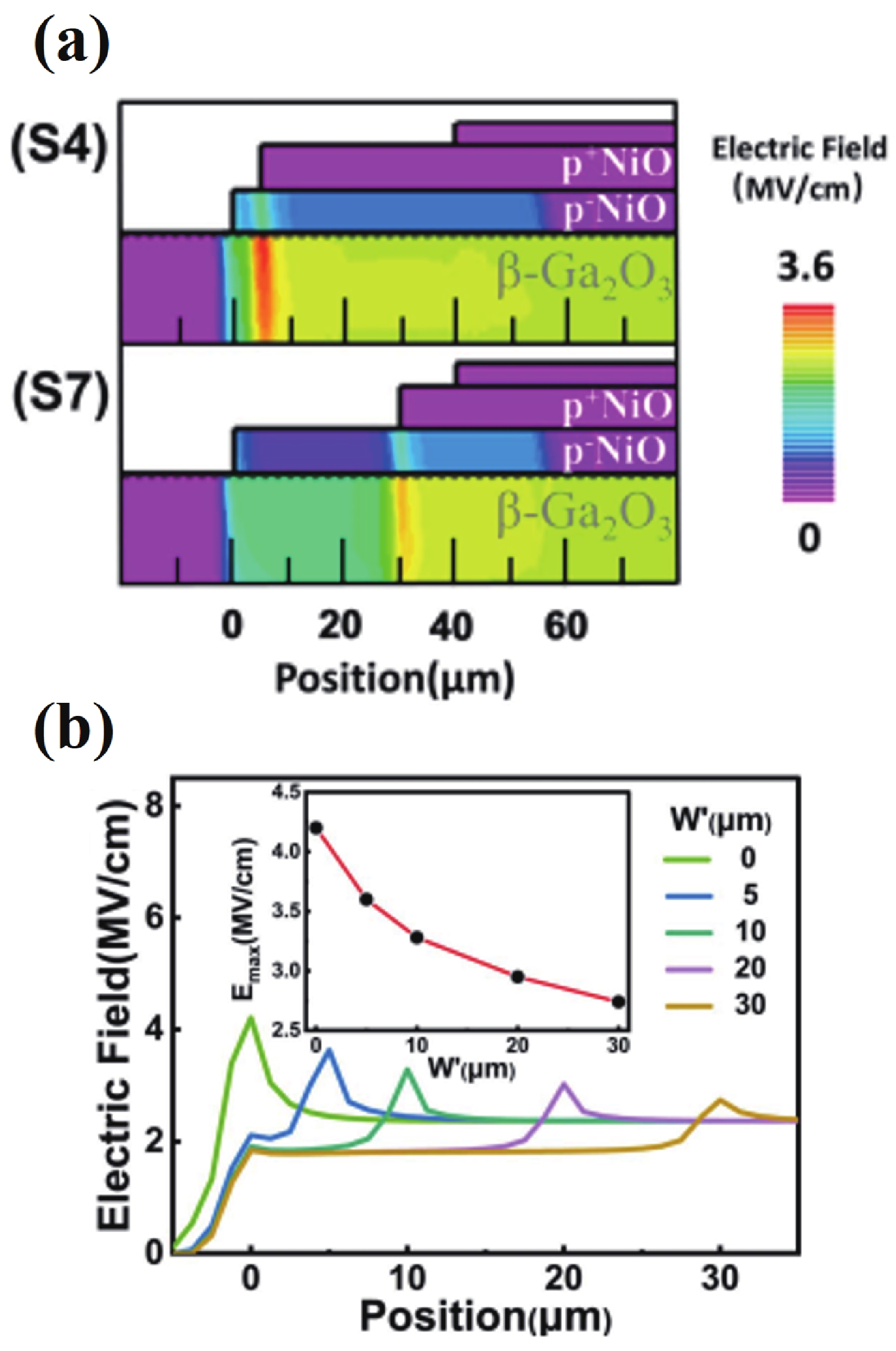
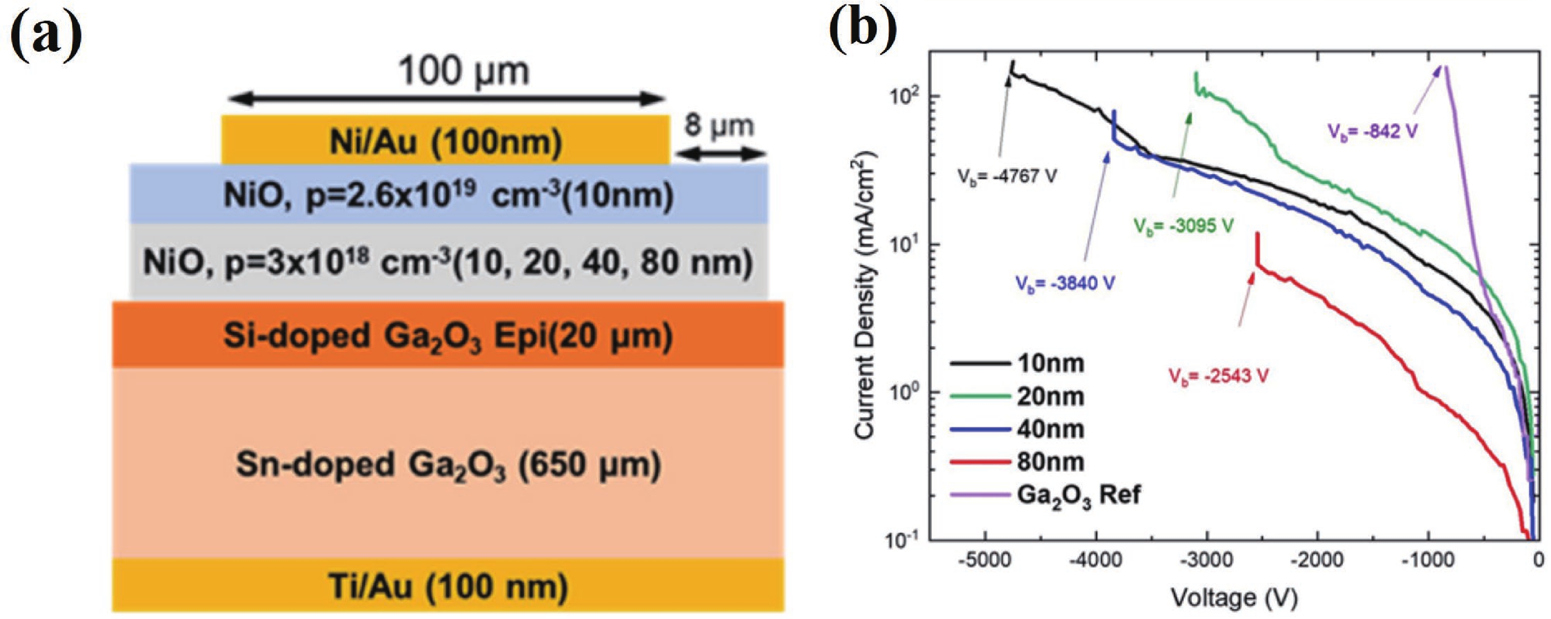
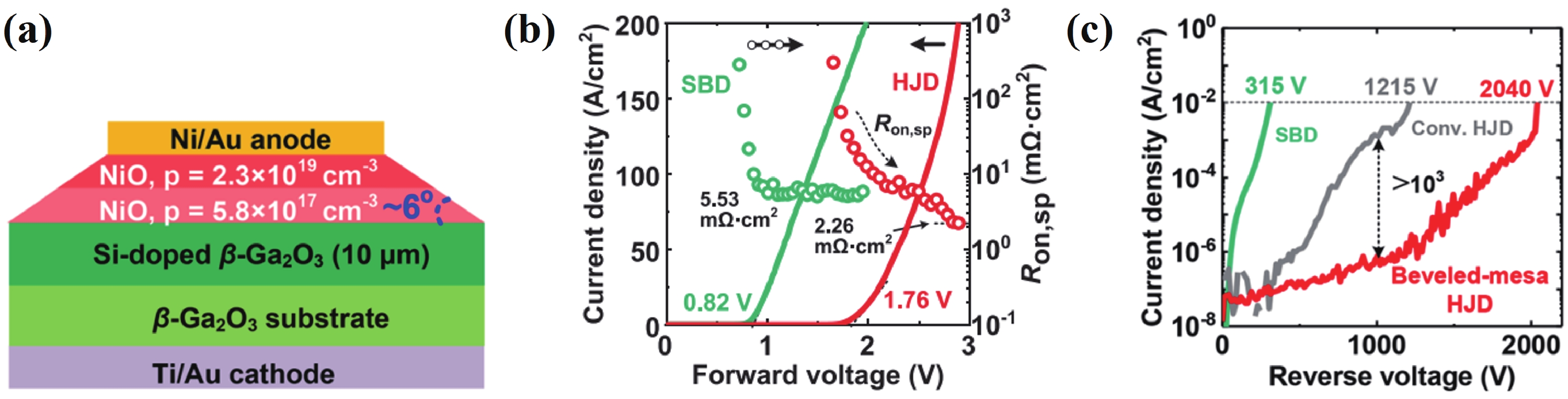
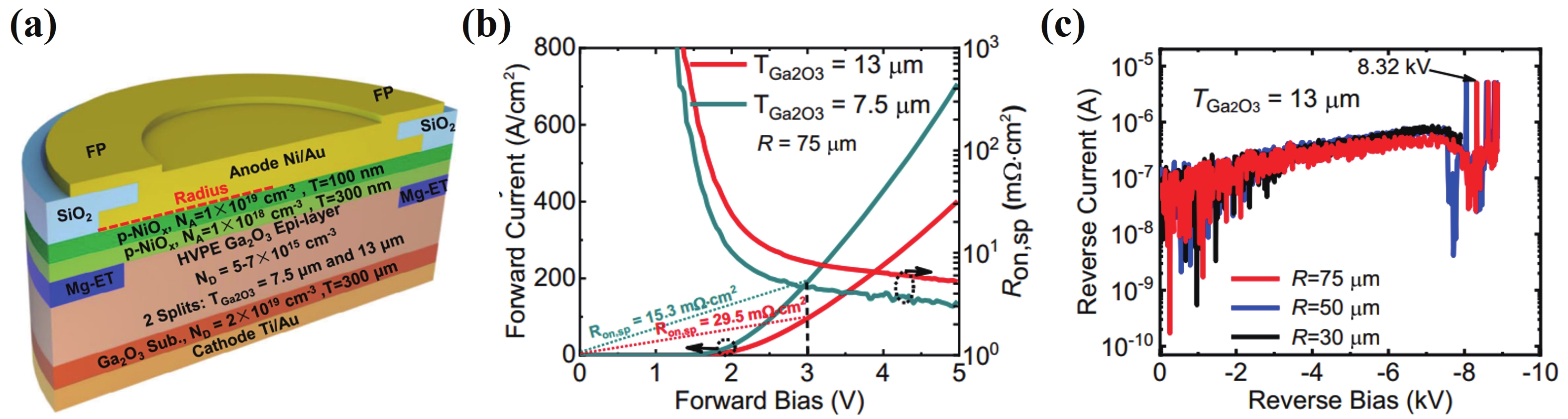
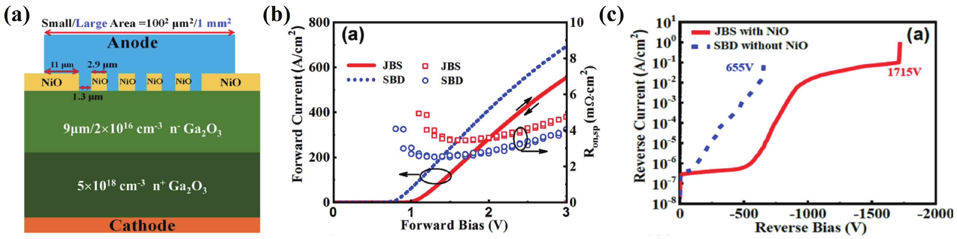
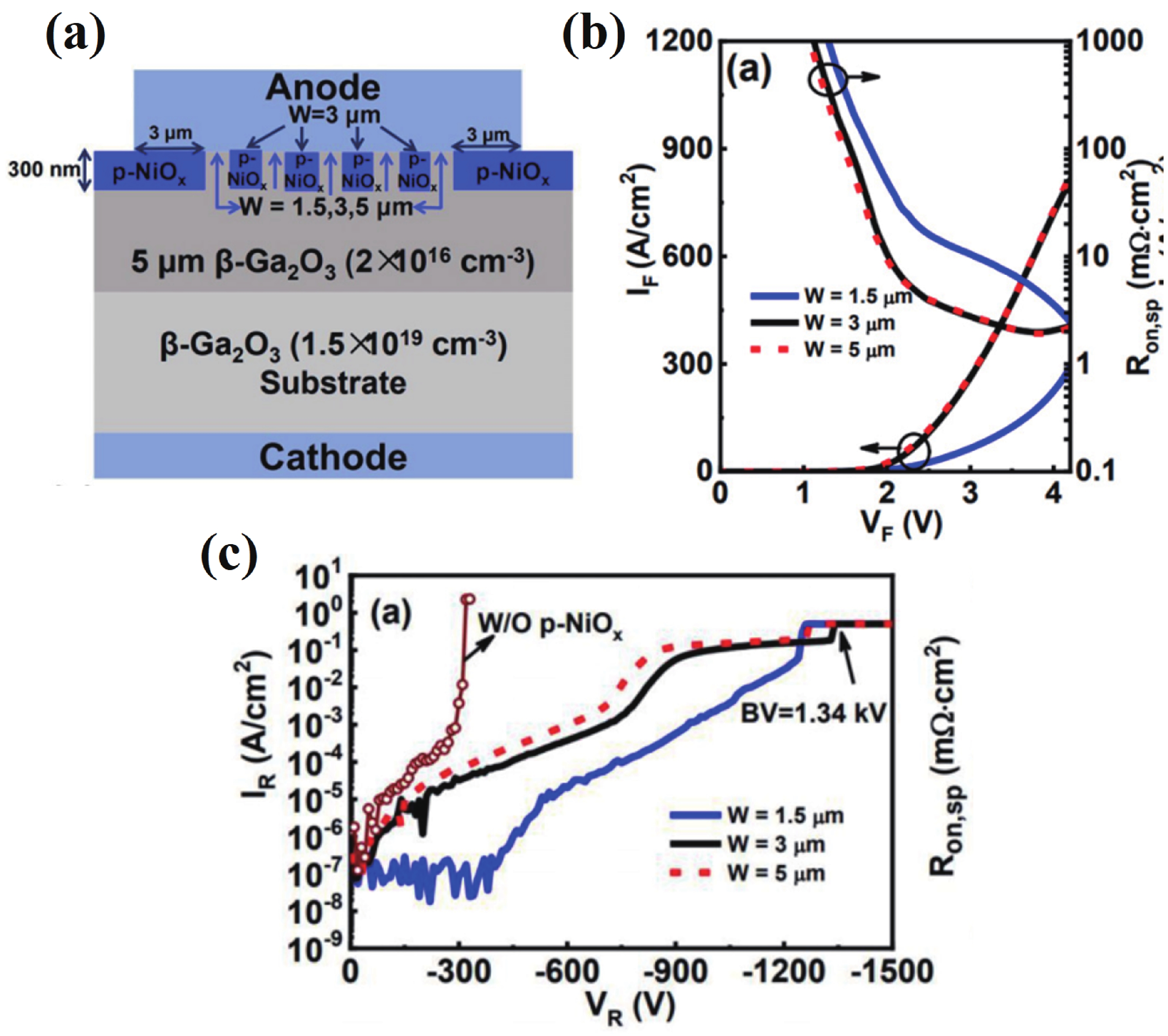
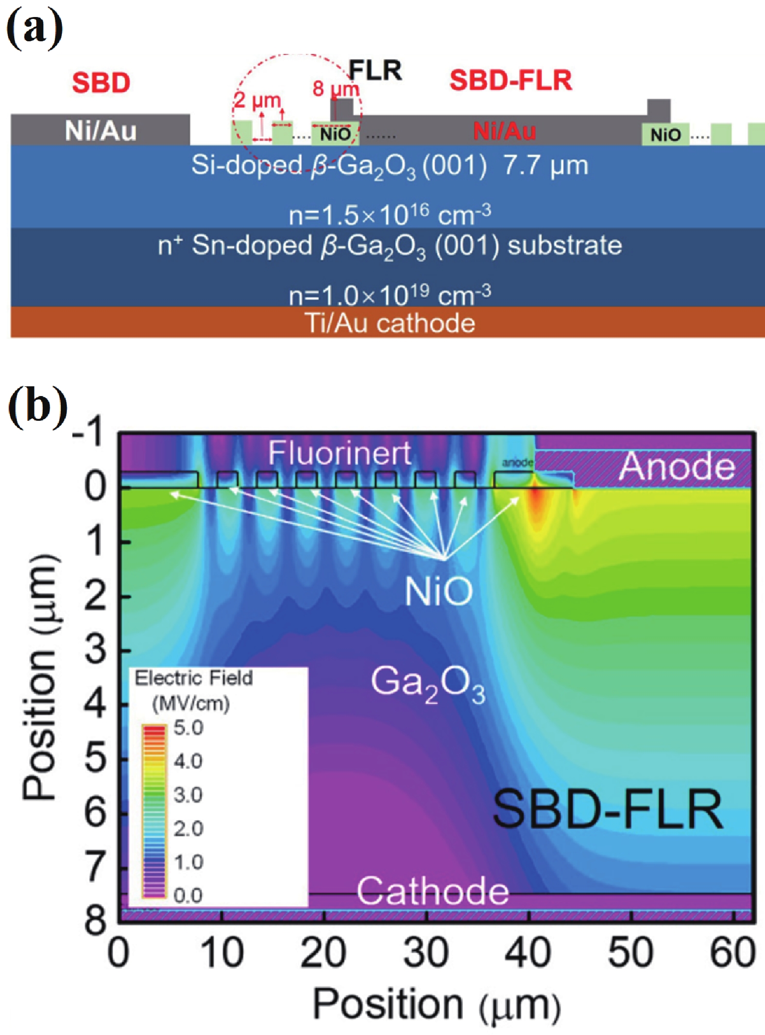
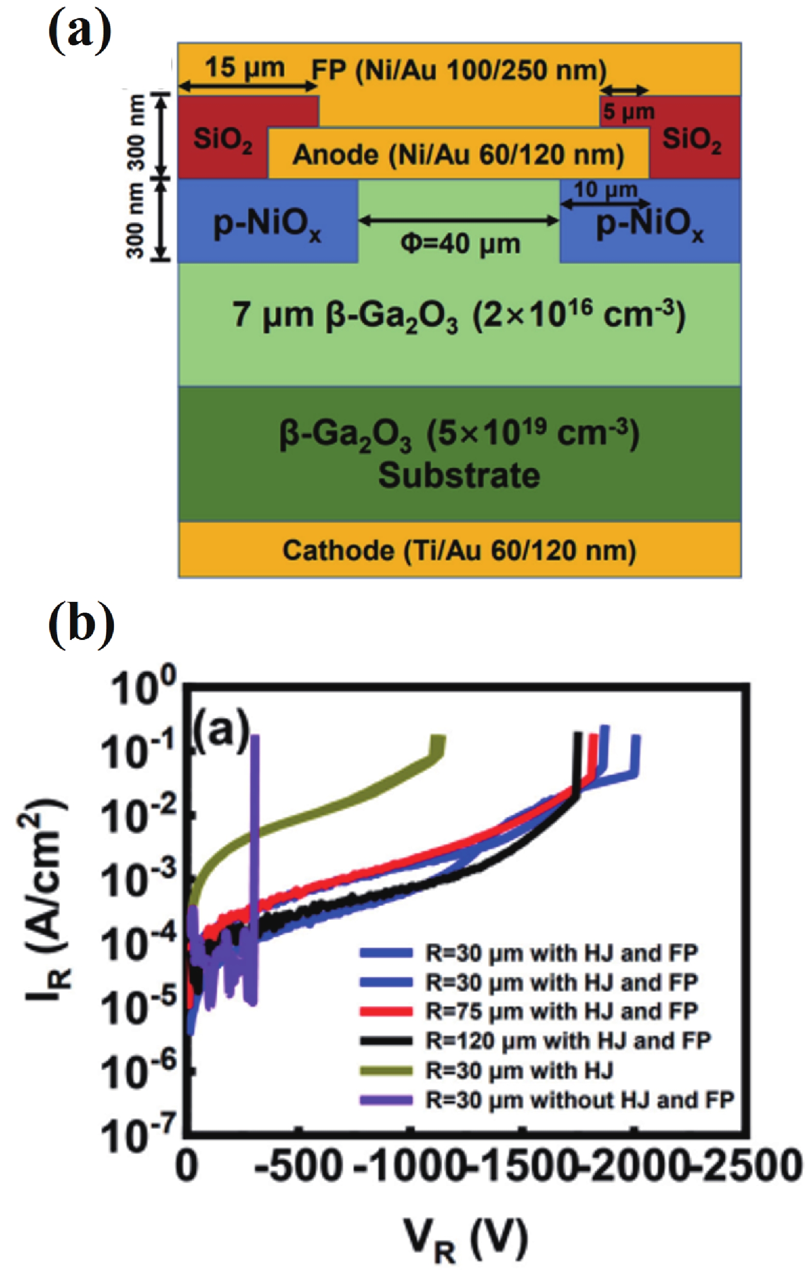
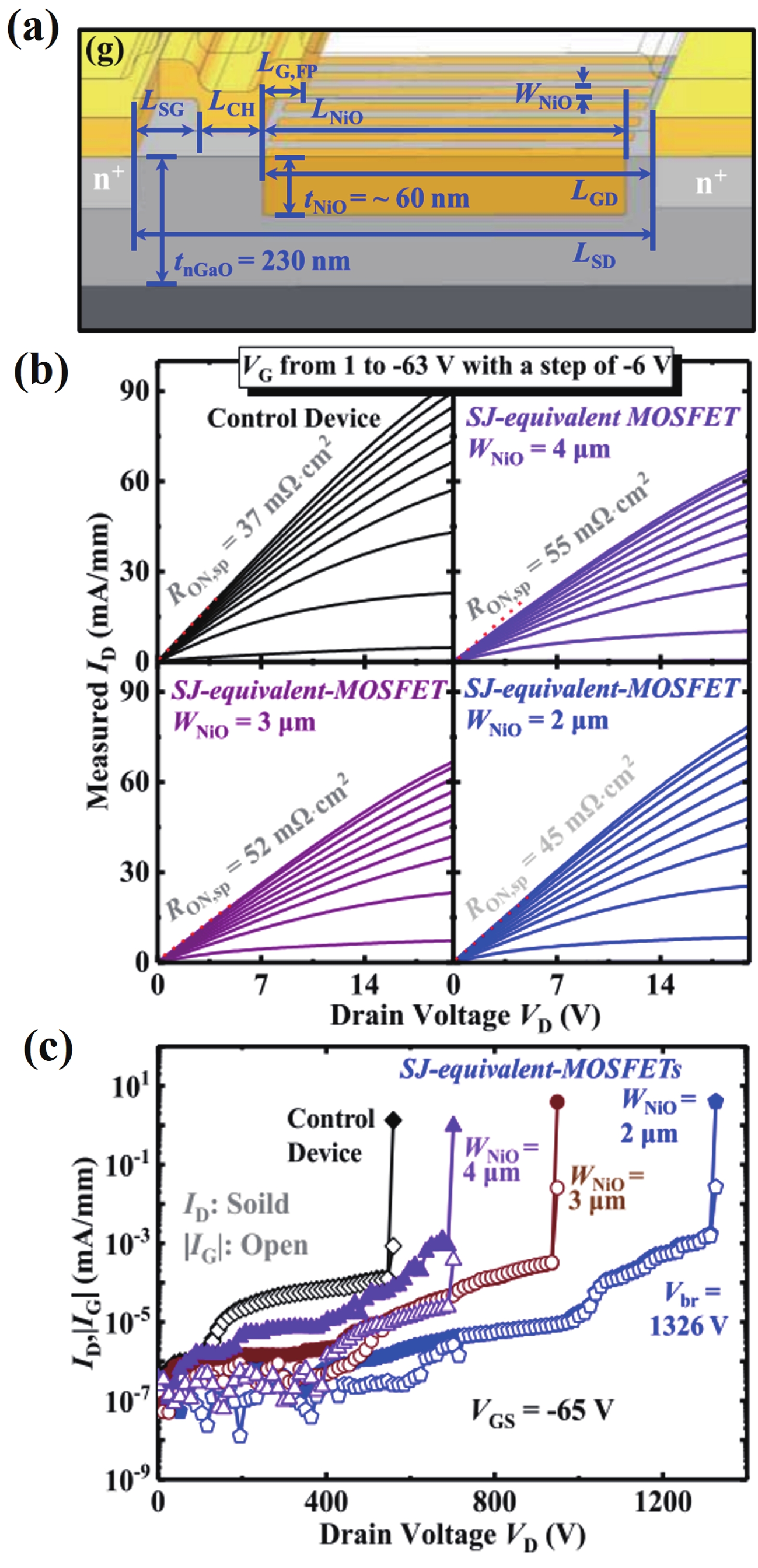
Beta gallium oxide (β-Ga2O3) has attracted significant attention for applications in power electronics due to its ultra-wide bandgap of ~ 4.8 eV and the large critical electric field of 8 MV/cm. These properties yield a high Baliga’s figures of merit (BFOM) of more than 3000. Though β-Ga2O3 possesses superior material properties, the lack of p-type doping is the main obstacle that hinders the development of β-Ga2O3-based power devices for commercial use. Constructing heterojunctions by employing other p-type materials has been proven to be a feasible solution to this issue. Nickel oxide (NiO) is the most promising candidate due to its wide band gap of 3.6–4.0 eV. So far, remarkable progress has been made in NiO/β-Ga2O3 heterojunction power devices. This review aims to summarize recent advances in the construction, characterization, and device performance of the NiO/β-Ga2O3 heterojunction power devices. The crystallinity, band structure, and carrier transport property of the sputtered NiO/β-Ga2O3 heterojunctions are discussed. Various device architectures, including the NiO/β-Ga2O3 heterojunction pn diodes (HJDs), junction barrier Schottky (JBS) diodes, and junction field effect transistors (JFET), as well as the edge terminations and super-junctions based on the NiO/β-Ga2O3 heterojunction, are described.

J. Semicond.
2023, 44(6): 062801 doi: 10.1088/1674-4926/44/6/062801
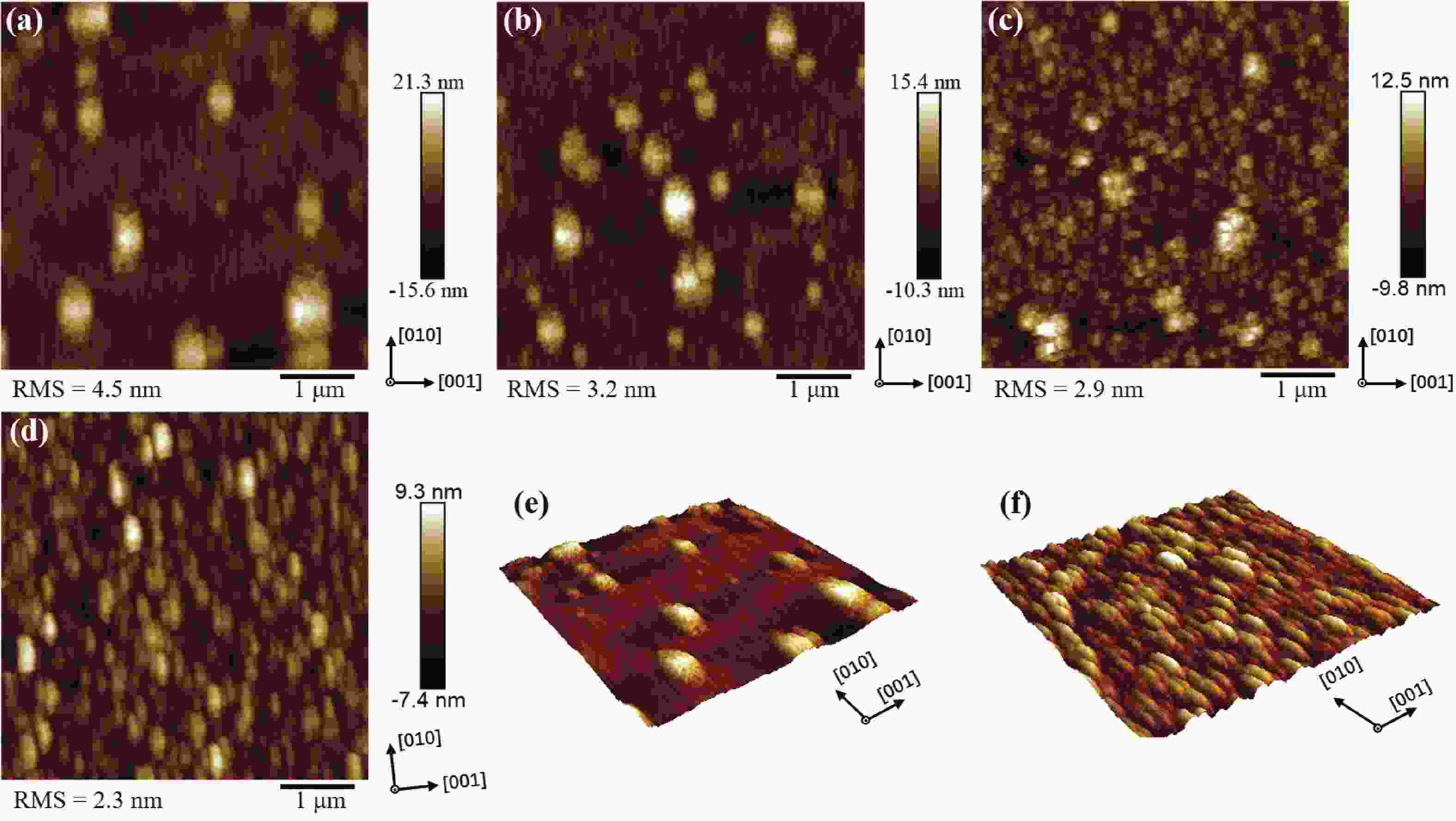
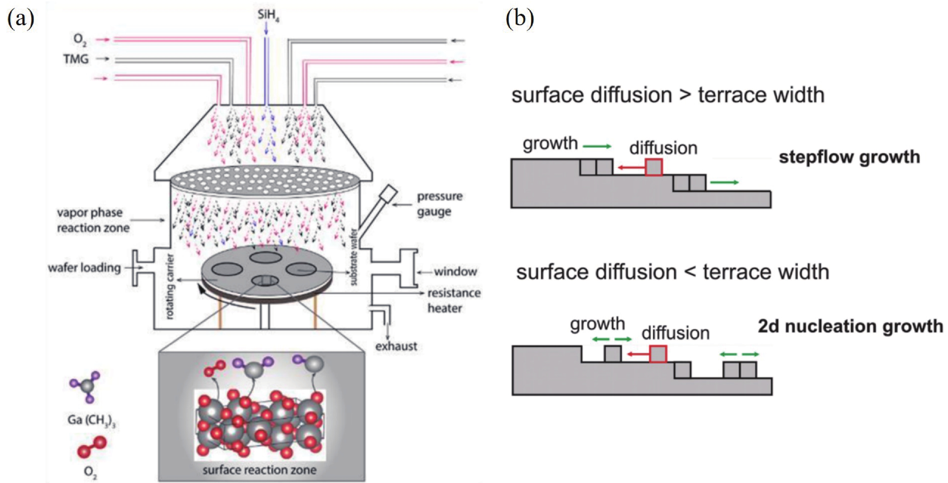
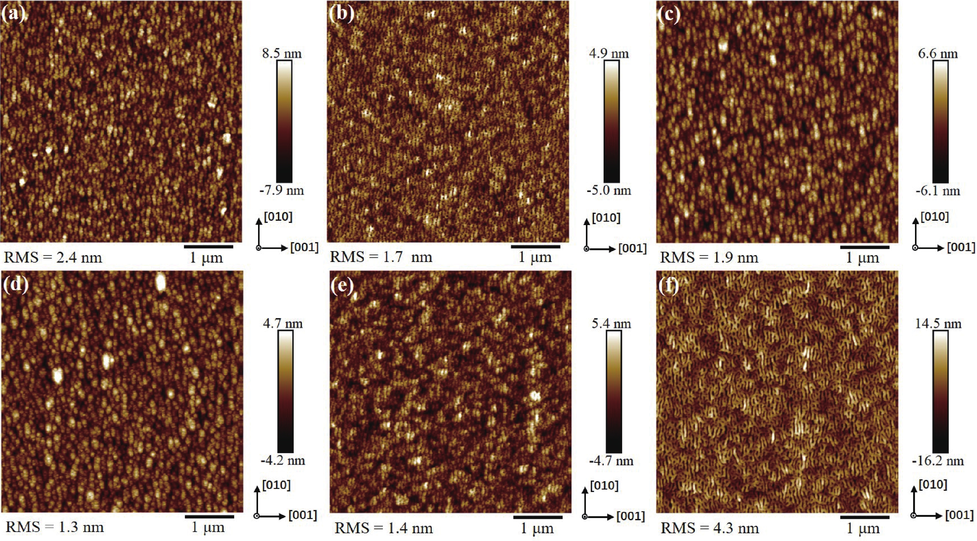
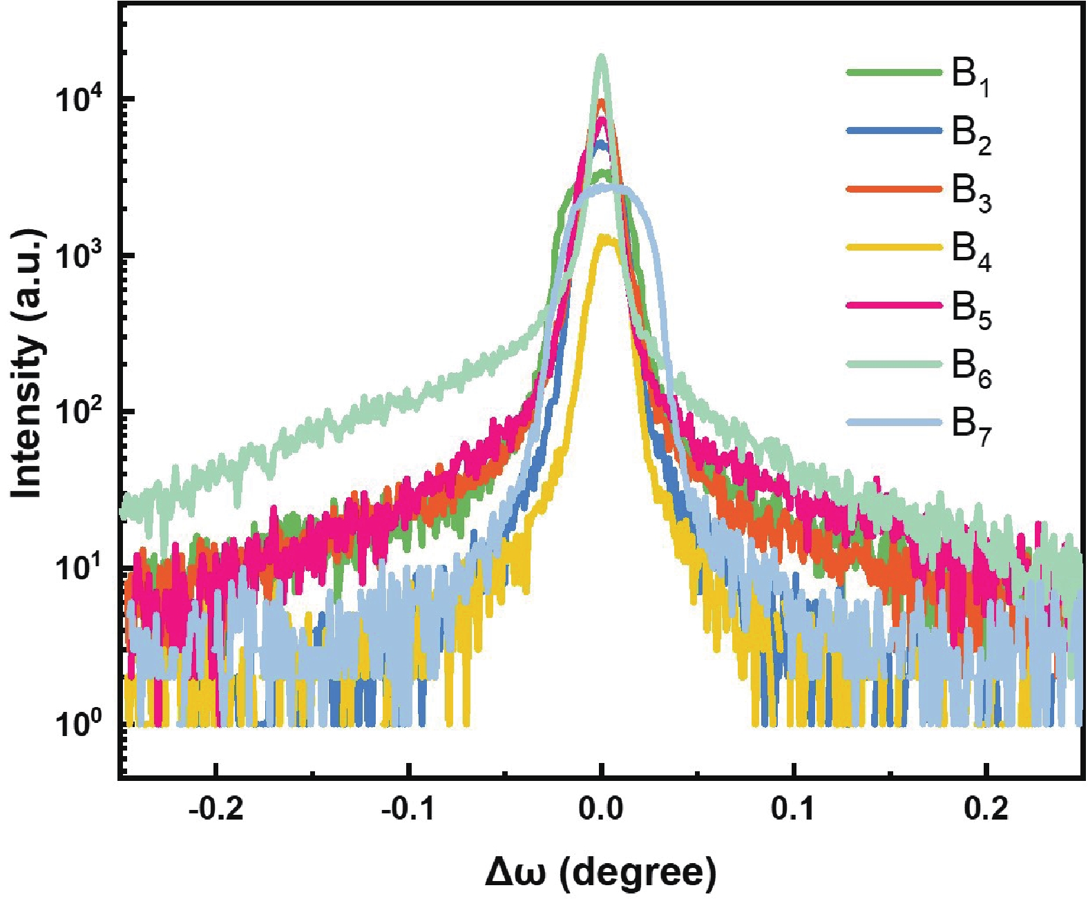
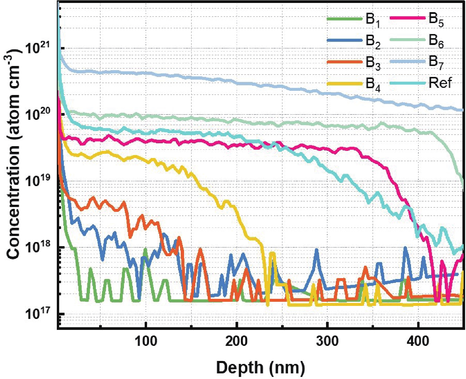
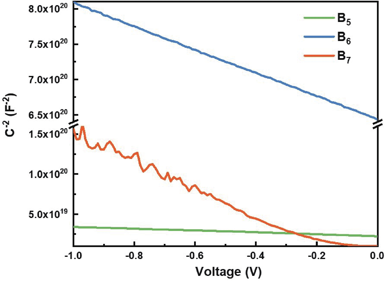
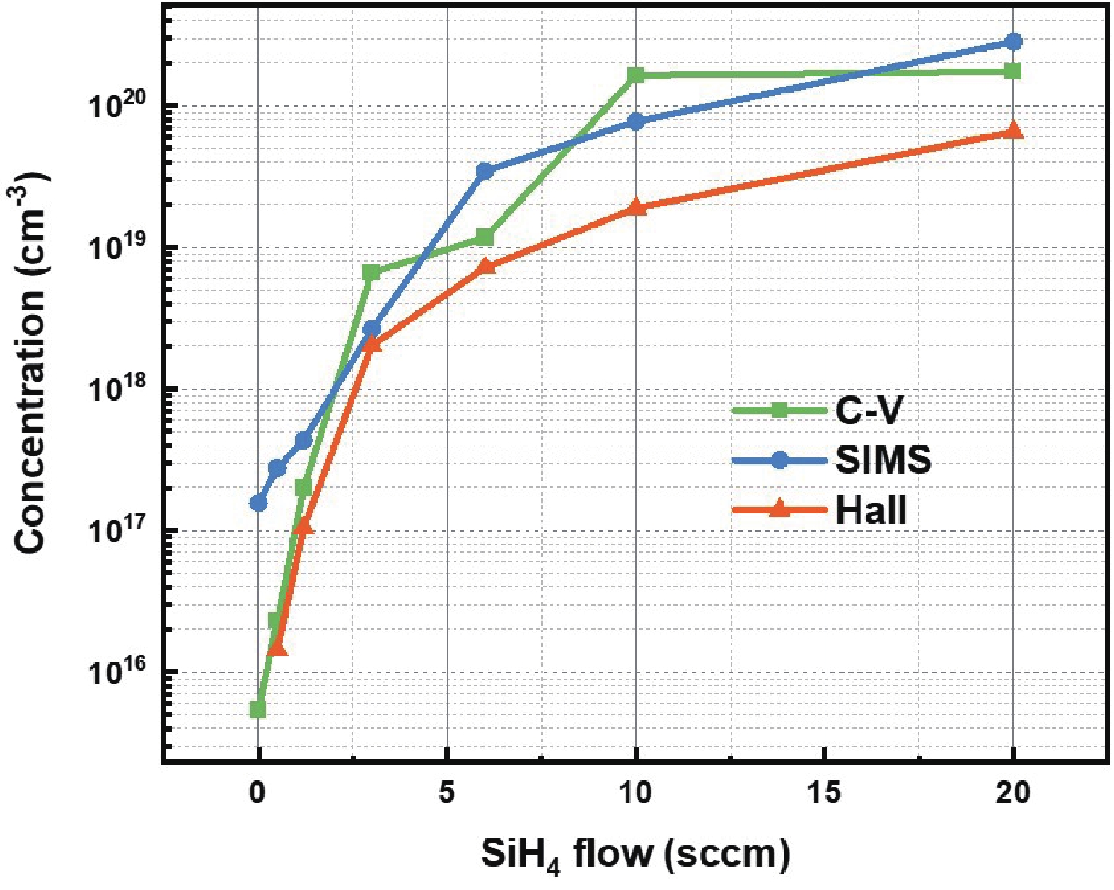
Homoepitaxial growth of Si-doped β-Ga2O3 films on semi-insulating (100) β-Ga2O3 substrates by metalorganic chemical vapor deposition (MOCVD) is studied in this work. By appropriately optimizing the growth conditions, an increasing diffusion length of Ga adatoms is realized, suppressing 3D island growth patterns prevalent in (100) β-Ga2O3 films and optimizing the surface morphology with [010] oriented stripe features. The slightly Si-doped β-Ga2O3 film shows smooth and flat surface morphology with a root-mean-square roughness of 1.3 nm. Rocking curves of the (400) diffraction peak also demonstrate the high crystal quality of the Si-doped films. According to the capacitance–voltage characteristics, the effective net doping concentrations of the films are 5.41 × 10¹⁵ – 1.74 × 1020 cm−3. Hall measurements demonstrate a high electron mobility value of 51 cm2/(V·s), corresponding to a carrier concentration of 7.19 × 1018 cm−3 and a high activation efficiency of up to 61.5%. Transmission line model (TLM) measurement shows excellent Ohmic contacts and a low specific contact resistance of 1.29 × 10⁻⁴ Ω·cm2 for the Si-doped film, which is comparable to the Si-implanted film with a concentration of 5.0 × 1019 cm−3, confirming the effective Si doing in the MOCVD epitaxy.

J. Semicond.
2023, 44(6): 062802 doi: 10.1088/1674-4926/44/6/062802

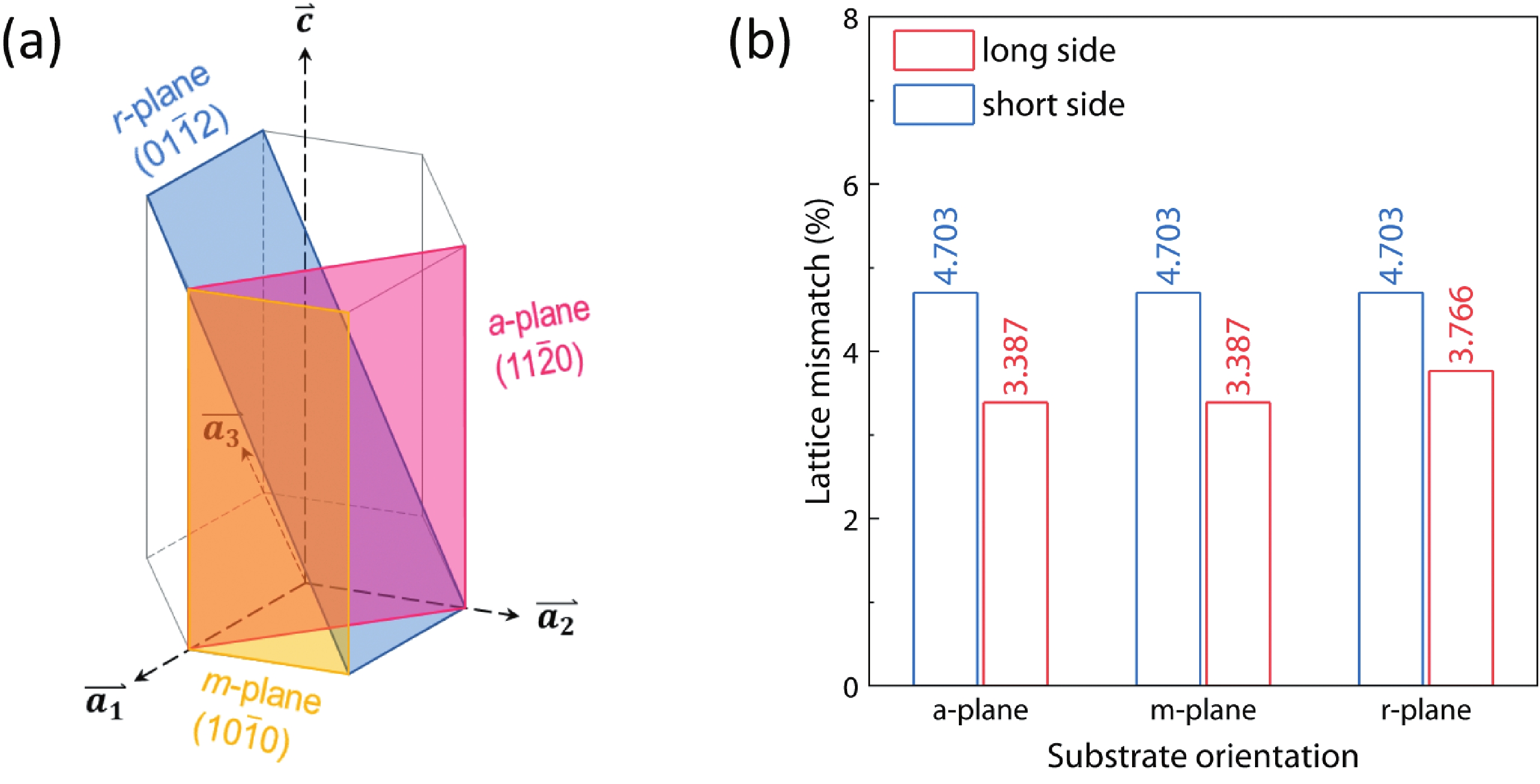
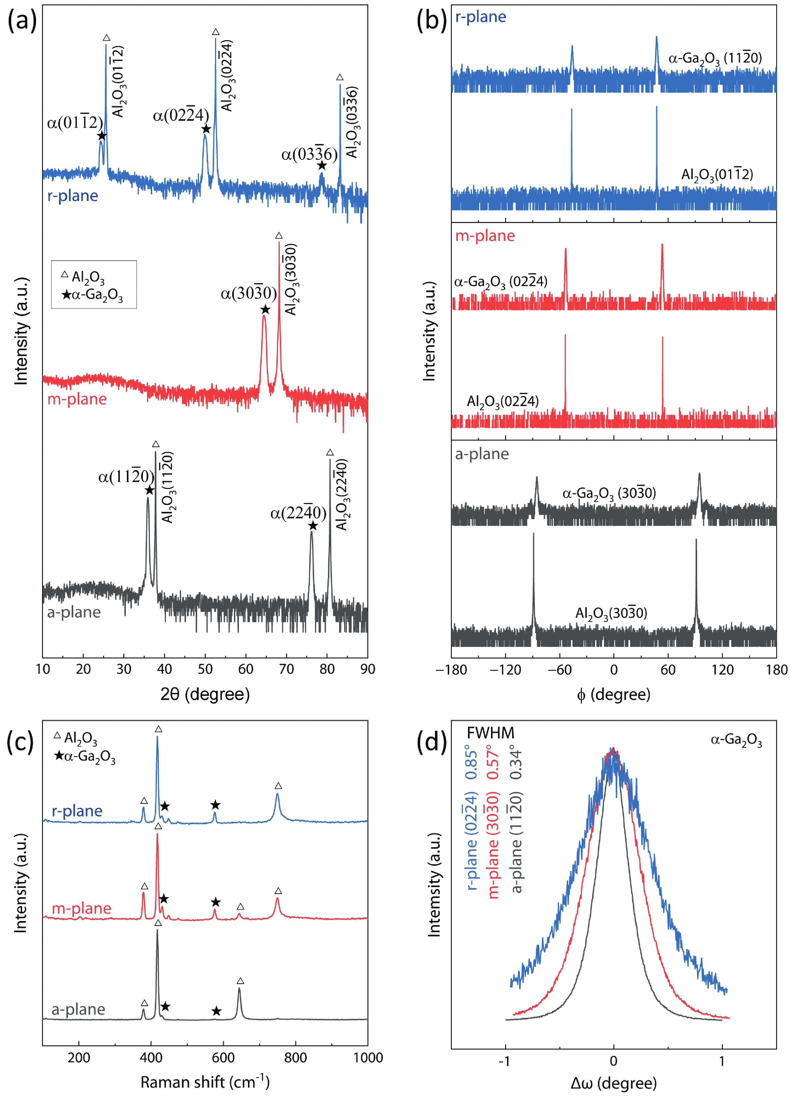
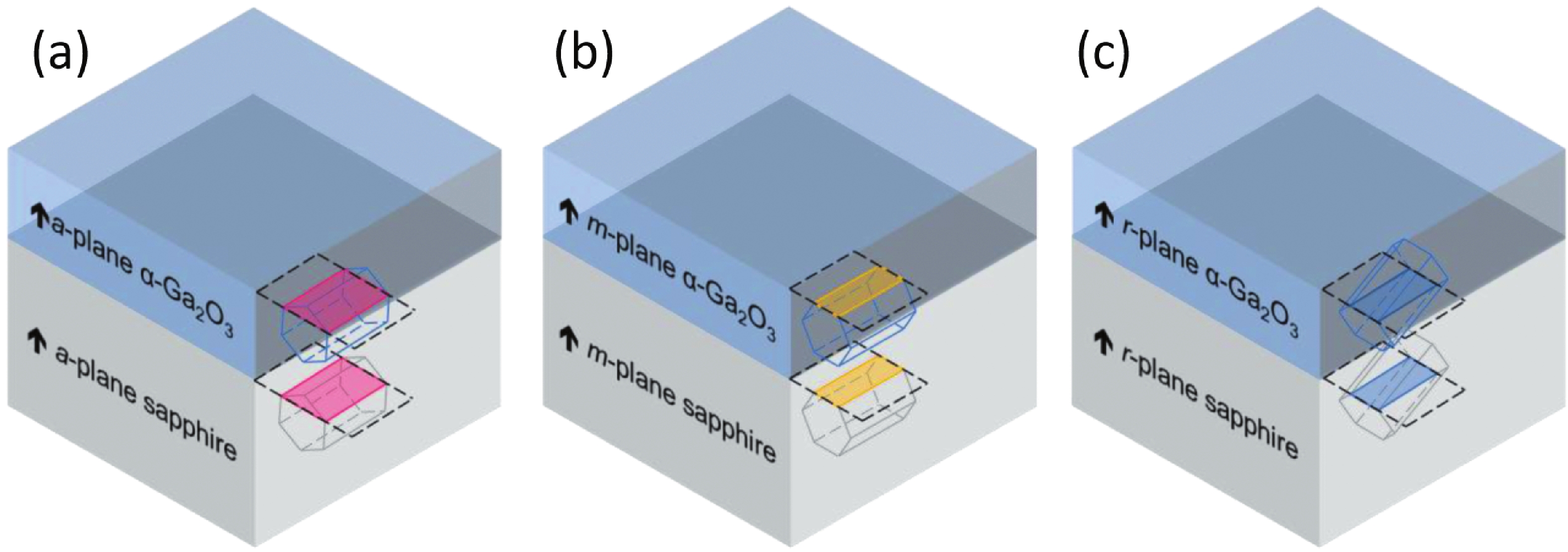
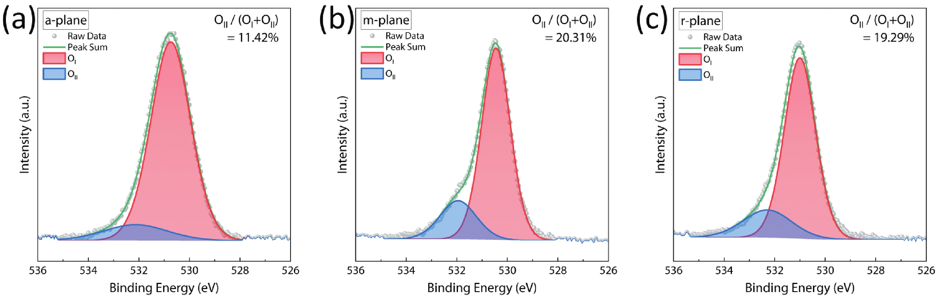
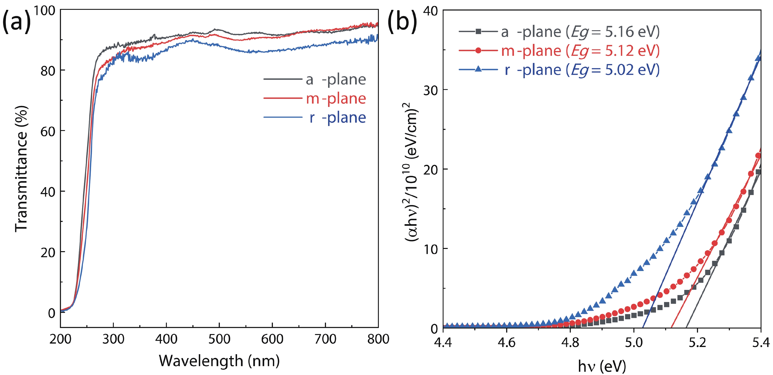
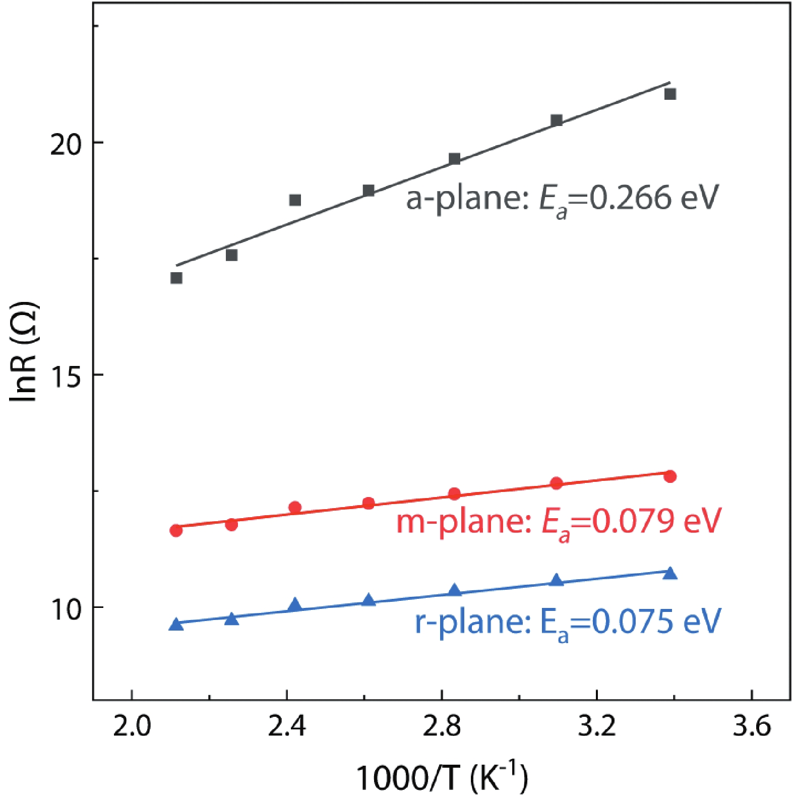
This study explores the epitaxial relationship and electrical properties of α-Ga2O3 thin films deposited on a-plane, m-plane, and r-plane sapphire substrates. We characterize the thin films by X-ray diffraction and Raman spectroscopy, and elucidate thin film epitaxial relationships with the underlying sapphire substrates. The oxygen vacancy concentration of α-Ga2O3 thin films on m-plane and r-plane sapphire substrates are higher than α-Ga2O3 thin film on a-plane sapphire substrates. All three thin films have a high transmission of over 80% in the visible and near-ultraviolet regions, and their optical bandgaps stay around 5.02–5.16 eV. Hall measurements show that the α-Ga2O3 thin film grown on r-plane sapphire has the highest conductivity of 2.71 S/cm, which is at least 90 times higher than the film on a-plane sapphire. A similar orientation-dependence is seen in their activation energy as revealed by temperature-dependent conductivity measurements, with 0.266, 0.079, and 0.075 eV for the film on a-, m-, r-plane, respectively. The origin of the distinct transport behavior of films on differently oriented substrates is suggested to relate with the distinct evolution of oxygen vacancies at differently oriented substrates. This study provides insights for the substrate selection when growing α-Ga2O3 films with tunable transport properties.
J. Semicond.
2023, 44(6): 062803 doi: 10.1088/1674-4926/44/6/062803
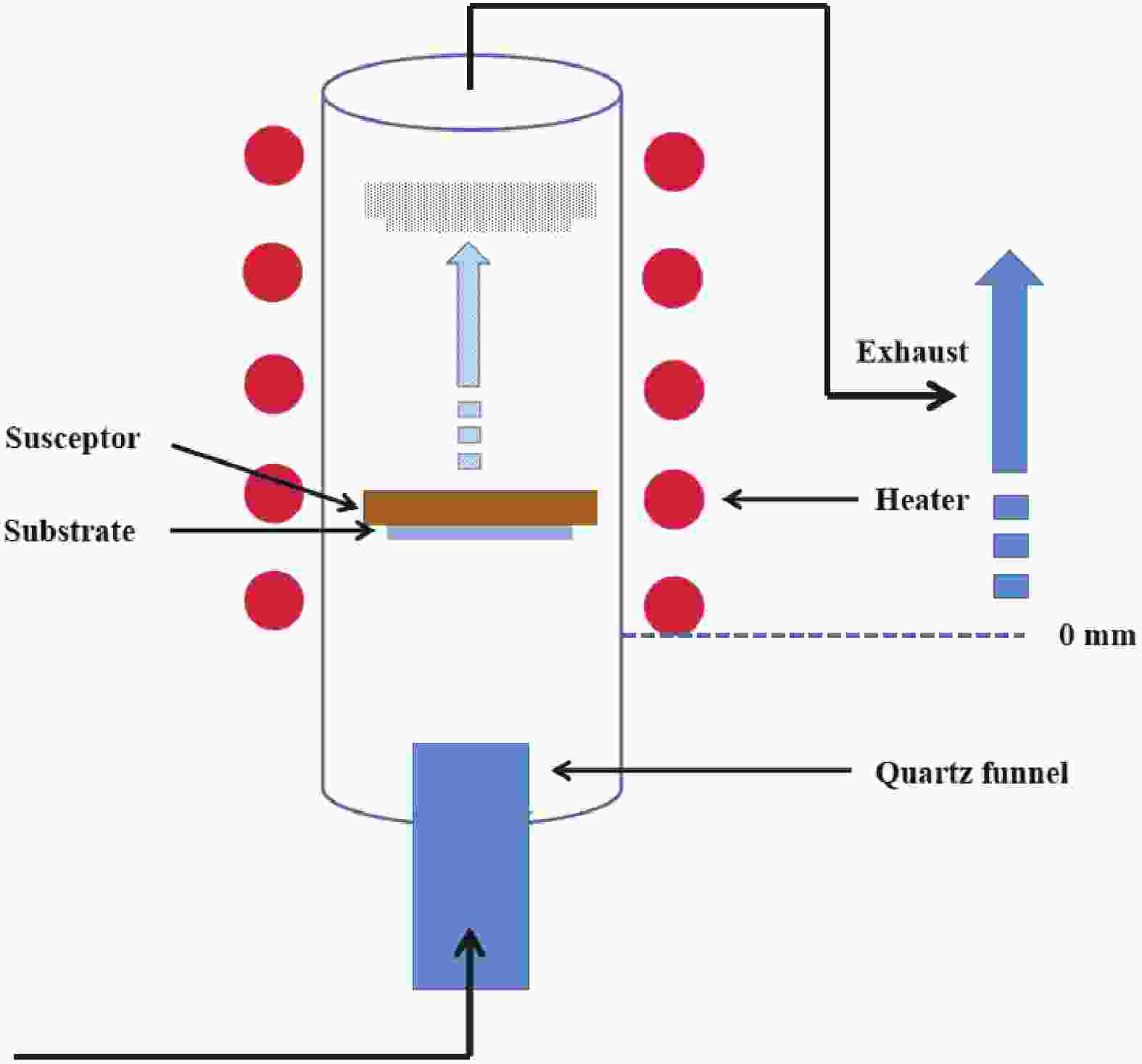
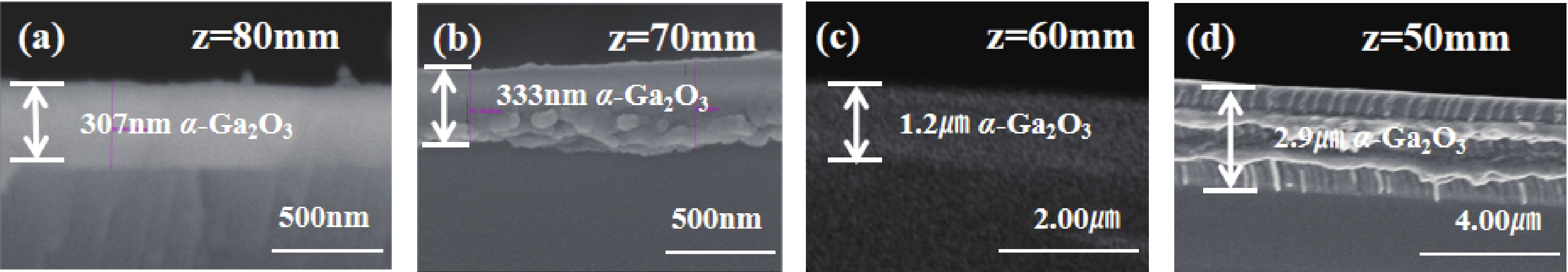
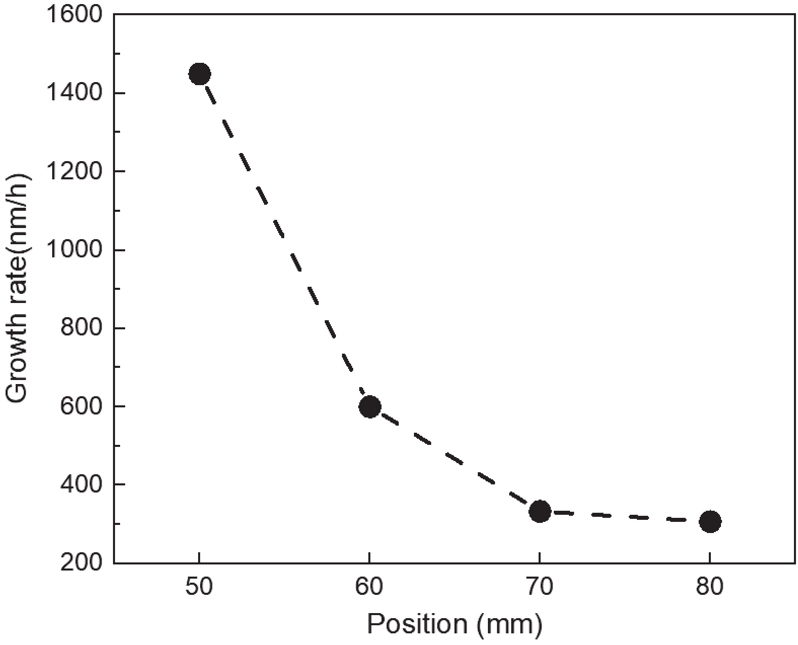
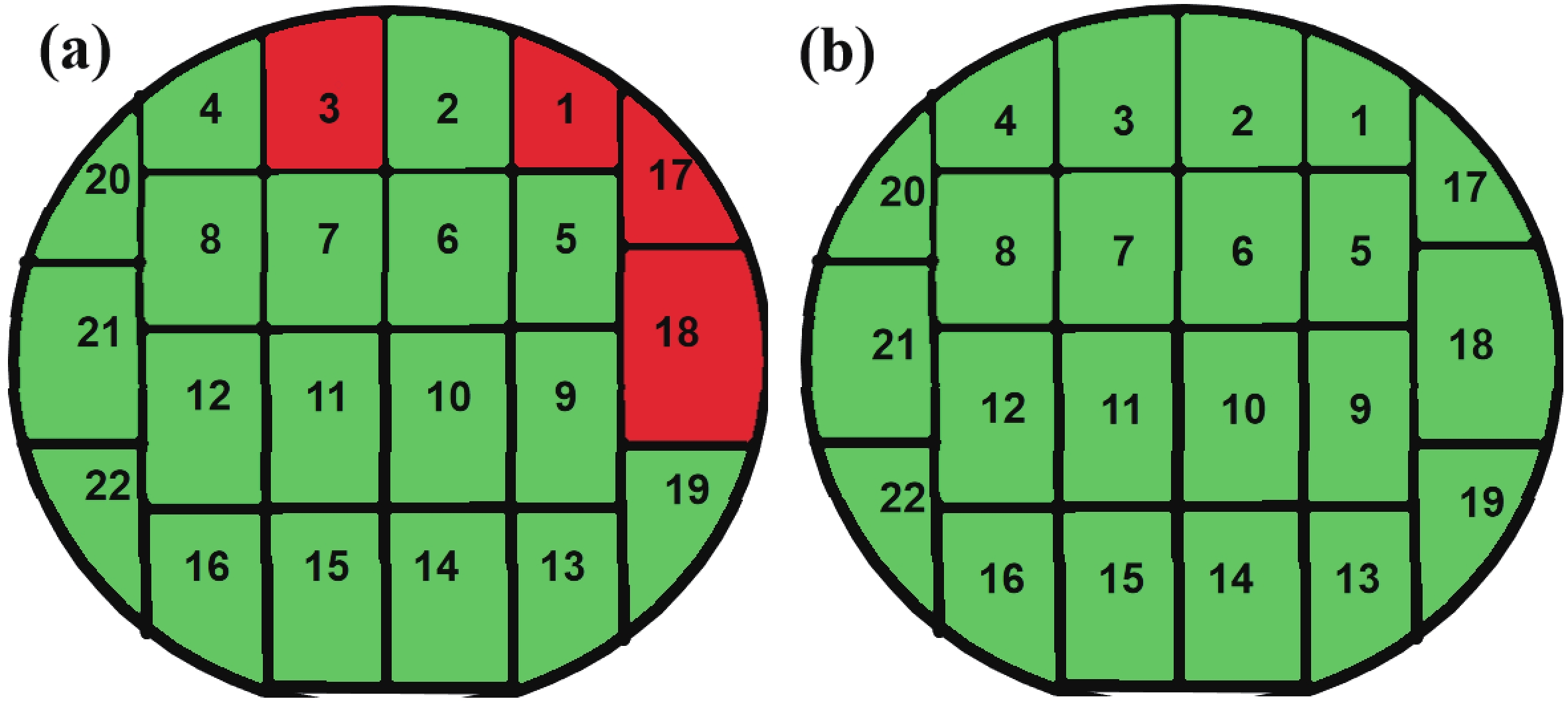
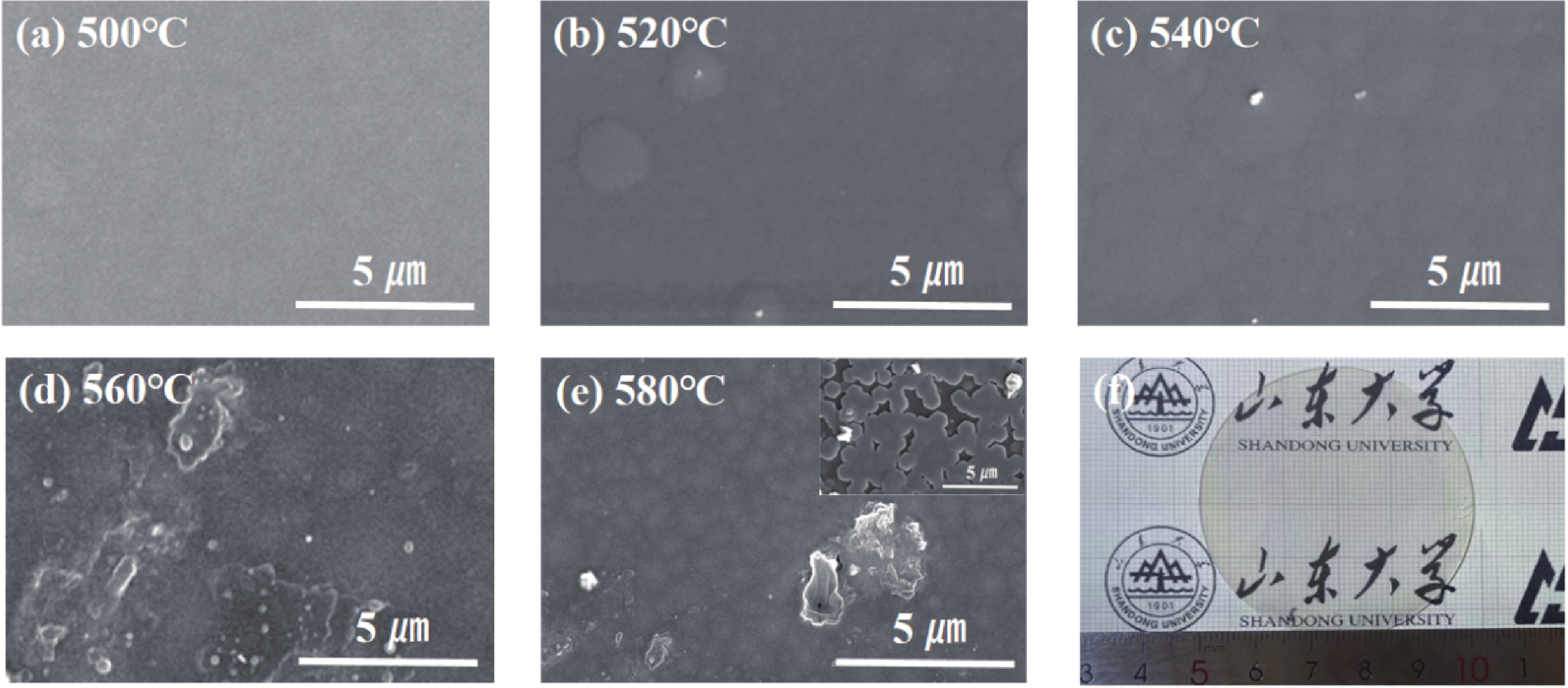
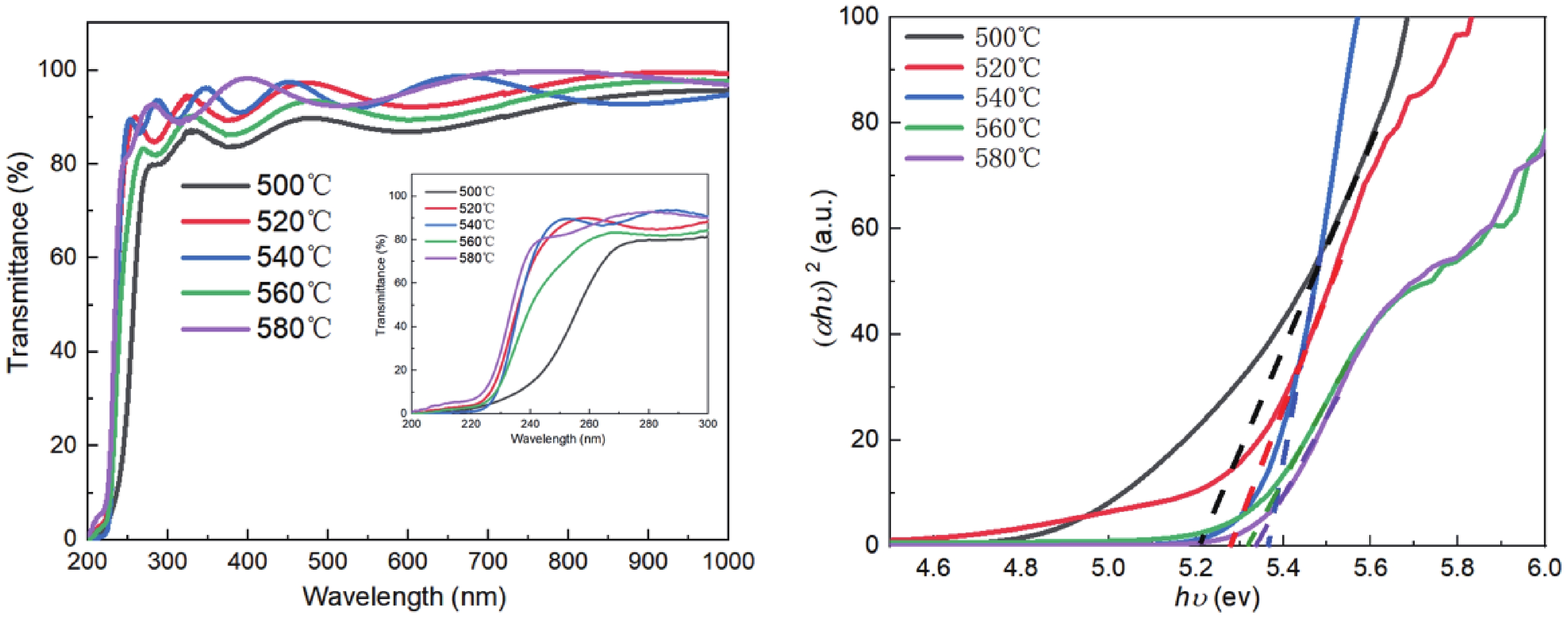
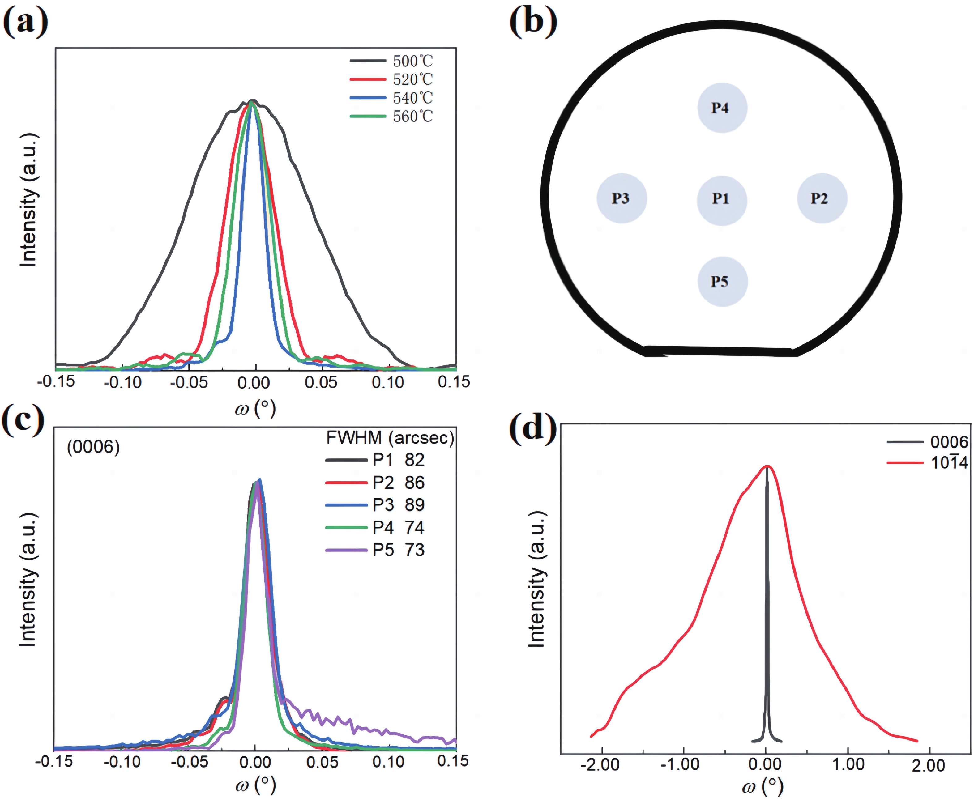
High thickness uniformity and large-scale films of α-Ga2O3 are crucial factors for the development of power devices. In this work, a high-quality 2-inch α-Ga2O3 epitaxial film on c-plane sapphire substrates was prepared by the mist-CVD method. The growth rate and phase control mechanisms were systematically investigated. The growth rate of the α-Ga2O3 films was limited by the evaporation of the microdroplets containing gallium acetylacetonate. By adjusting the substrate position (z) from 80 to 50 mm, the growth rate was increased from 307 nm/h to 1.45 μm/h when the growth temperature was fixed at 520 °C. When the growth temperature exceeded 560 °C, ε-Ga2O3 was observed to form at the edges of 2-inch sapphire substrate. Phase control was achieved by adjusting the growth temperature. When the growth temperature was 540 °C and the substrate position was 50 mm, the full-width at half maximum (FWHM) of the rocking curves for the (0006) and (10-14) planes were 0.023° and 1.17°. The screw and edge dislocations were 2.3 × 10⁶ and 3.9 × 1010 cm-2, respectively. Furthermore, the bandgaps and optical transmittance of α-Ga2O3 films grown under different conditions were characterized utilizing UV-visible and near-IR scanning spectra.


J. Semicond.
2023, 44(6): 062804 doi: 10.1088/1674-4926/44/6/062804
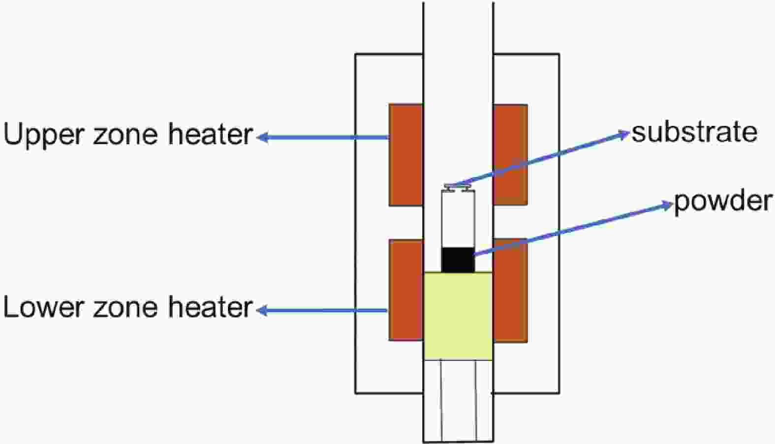
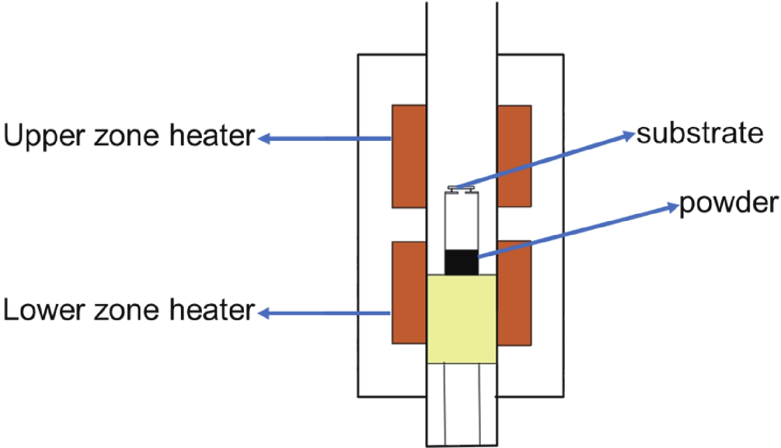
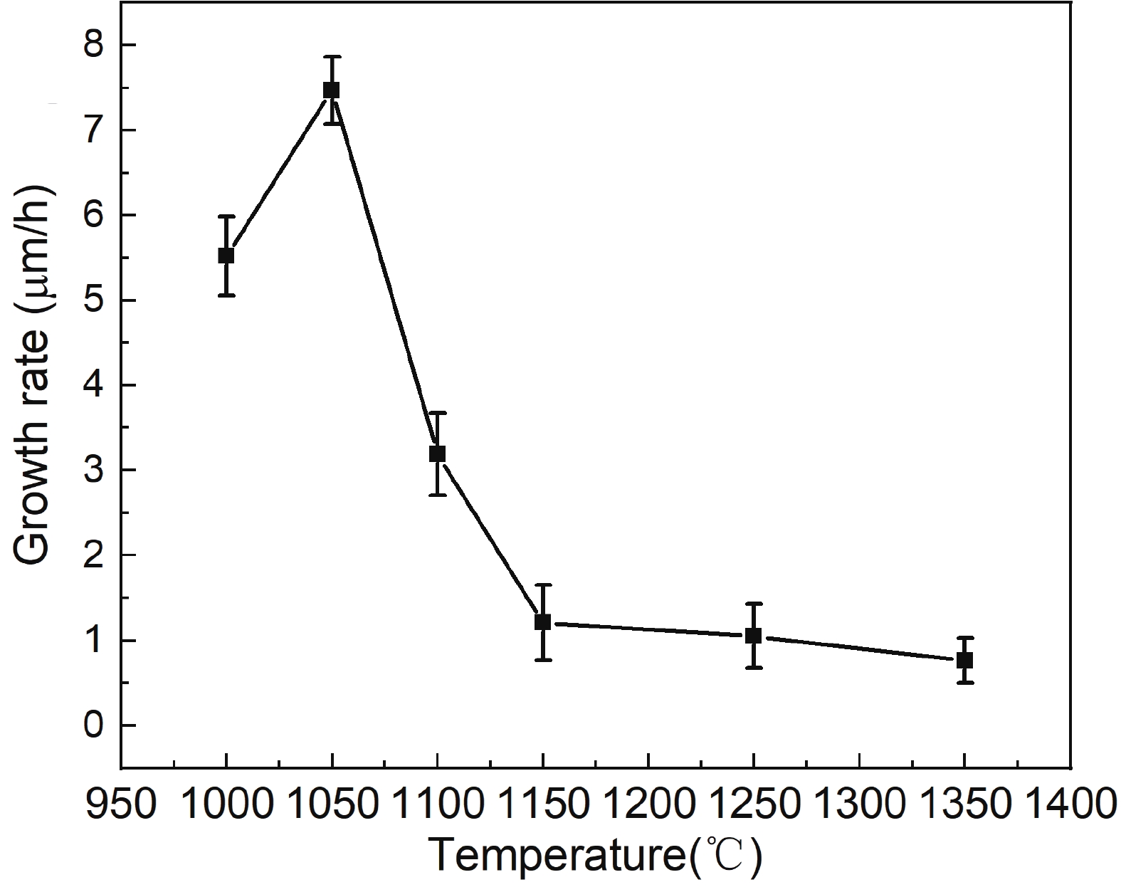
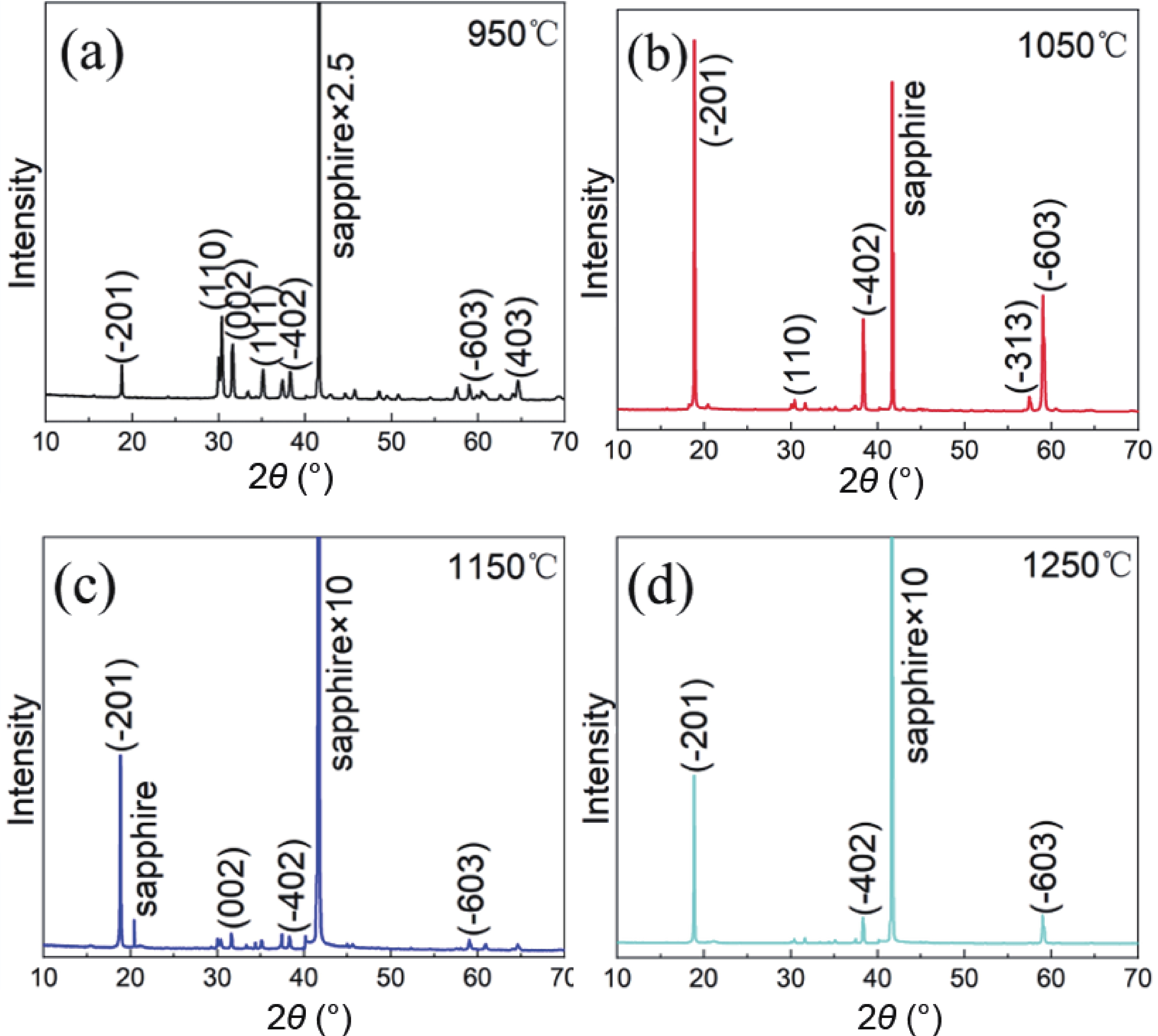
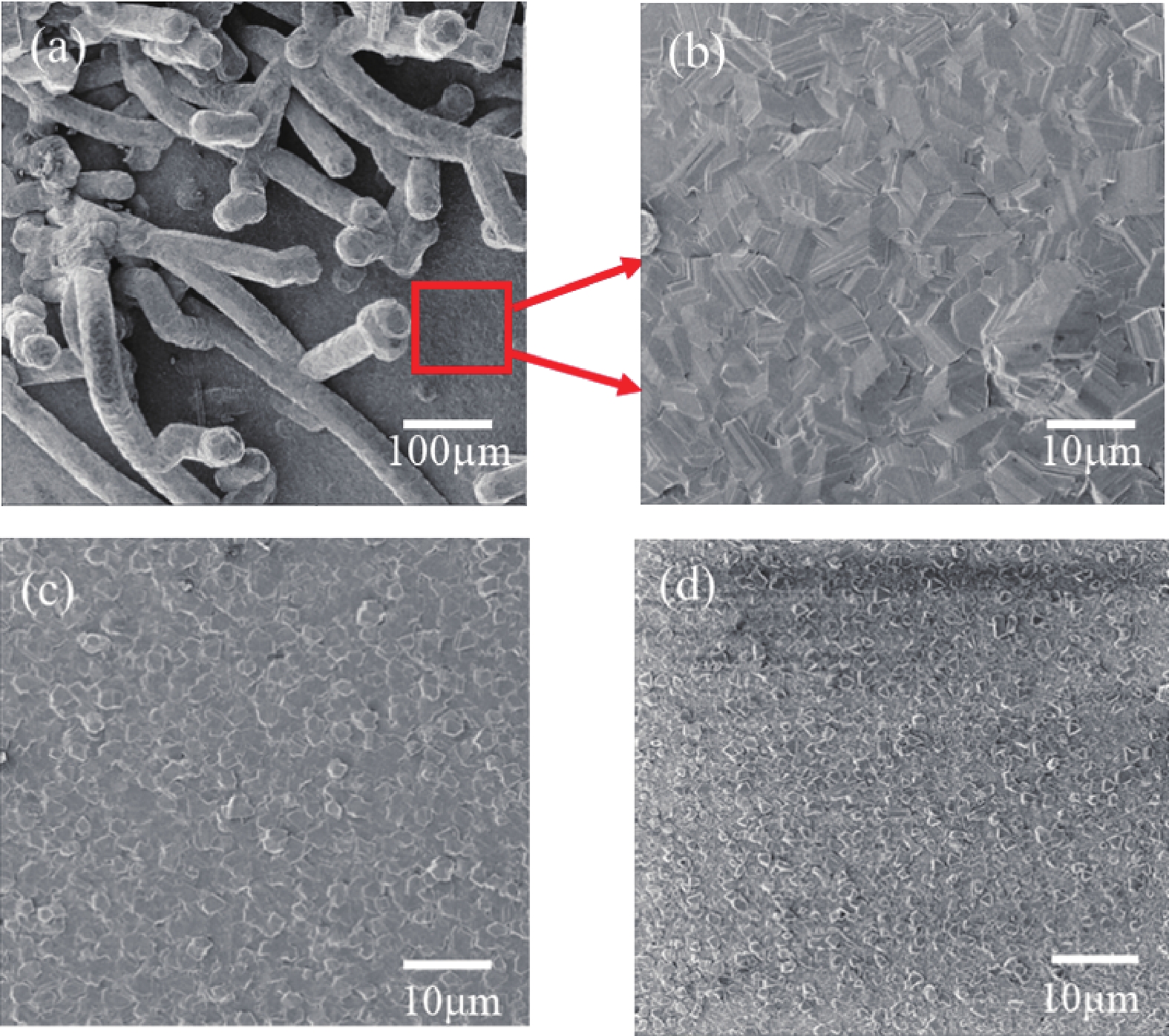
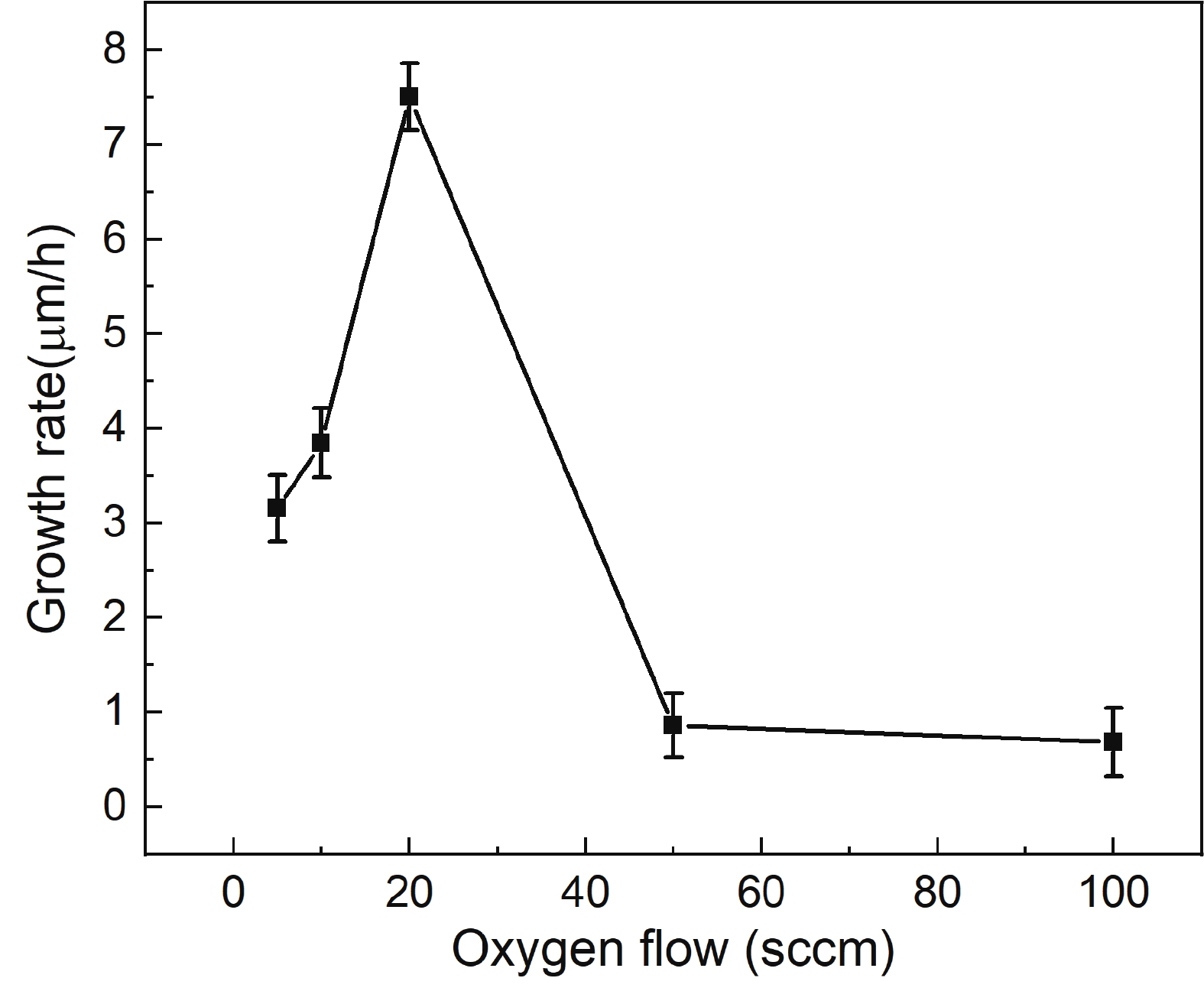
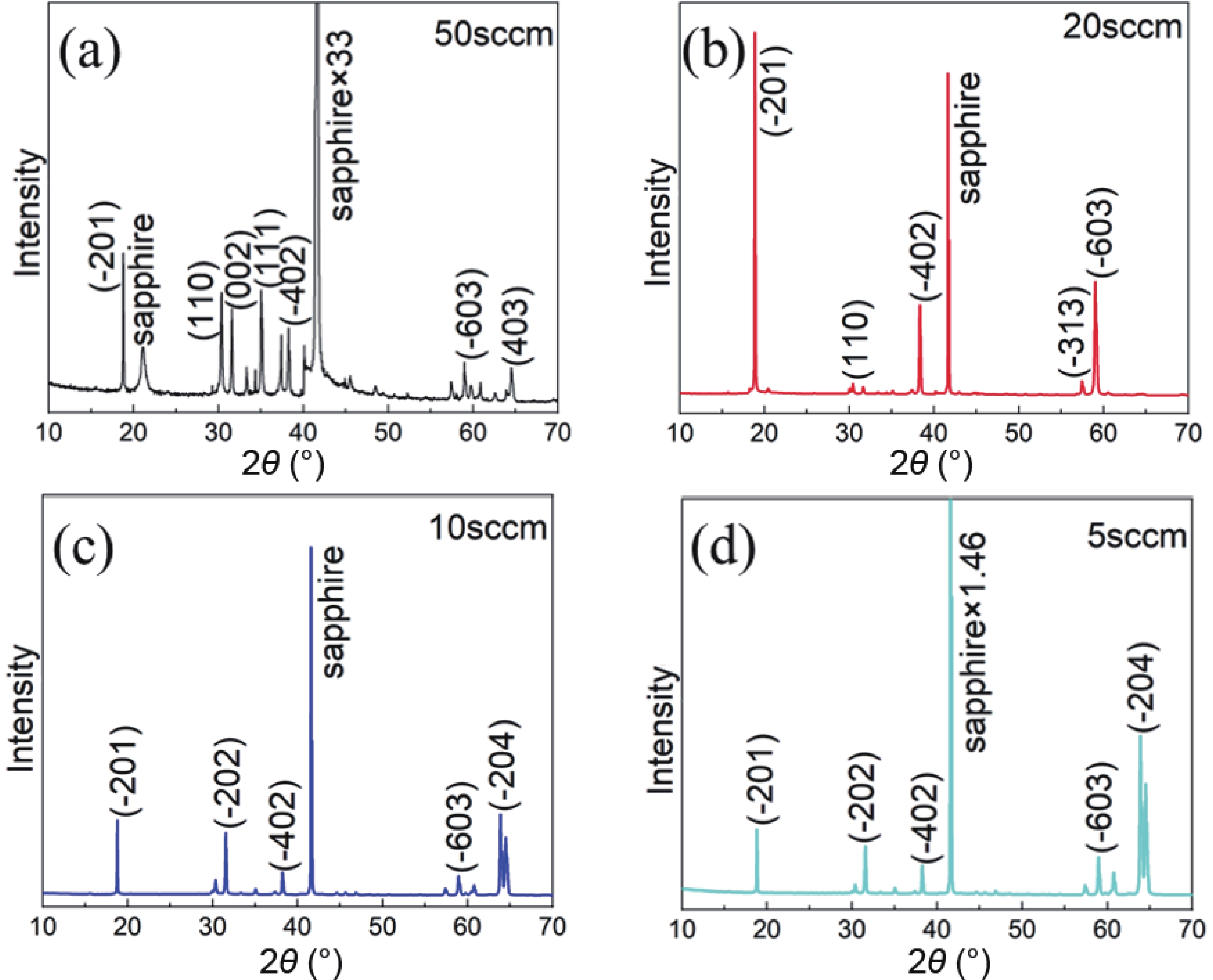
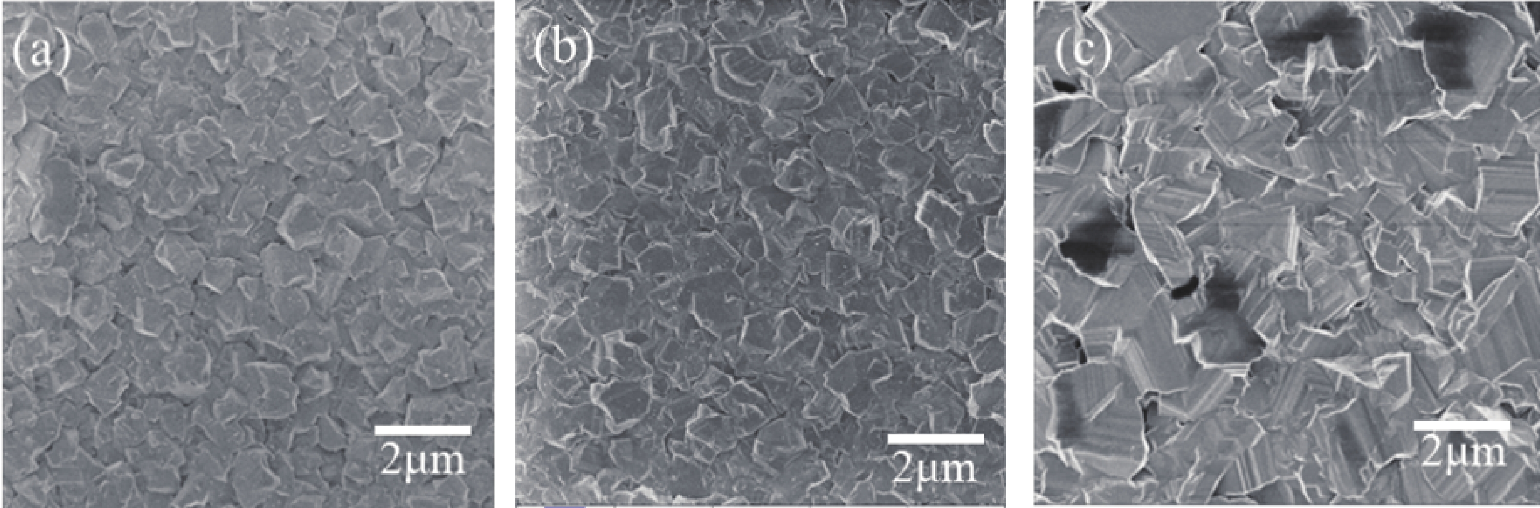
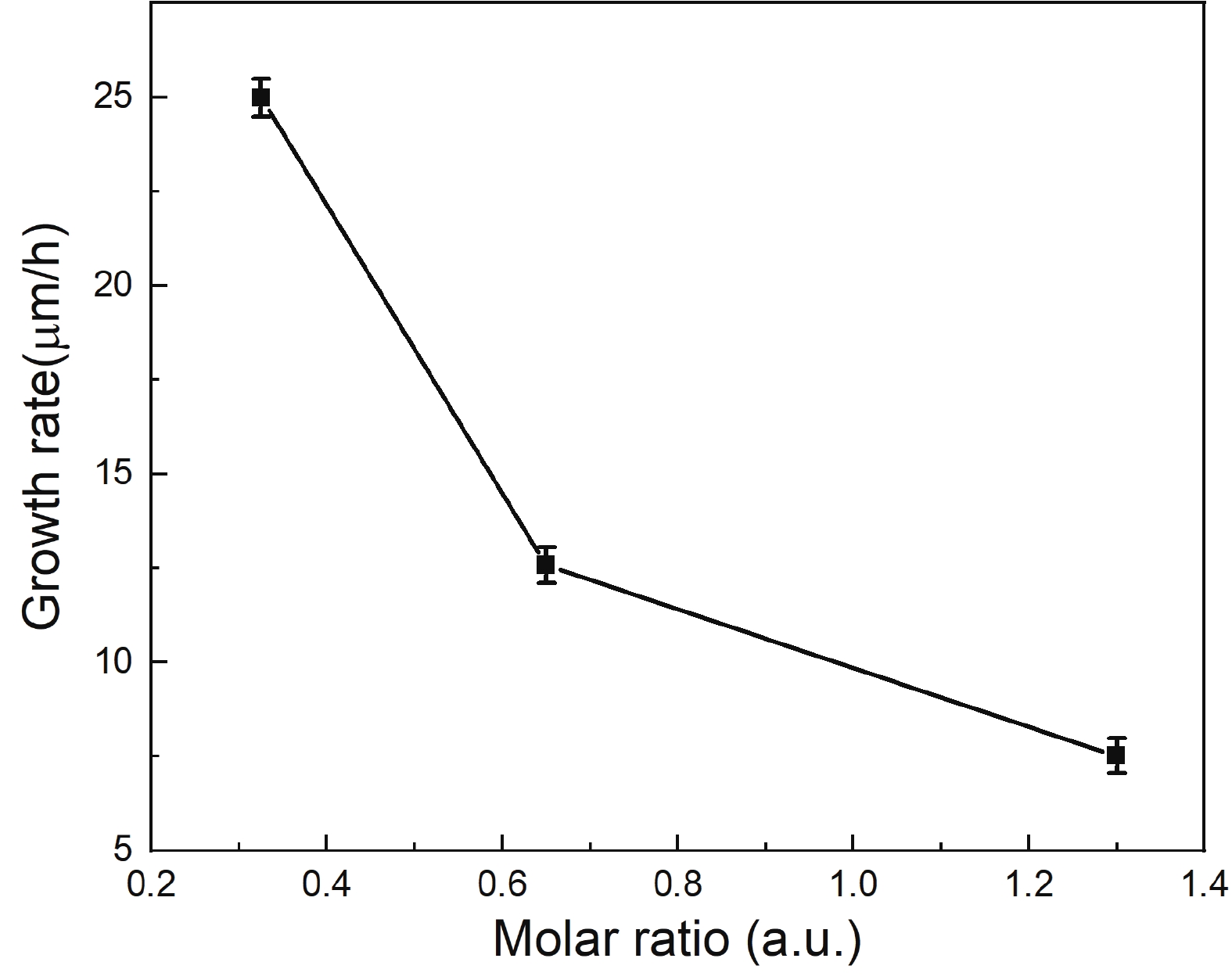
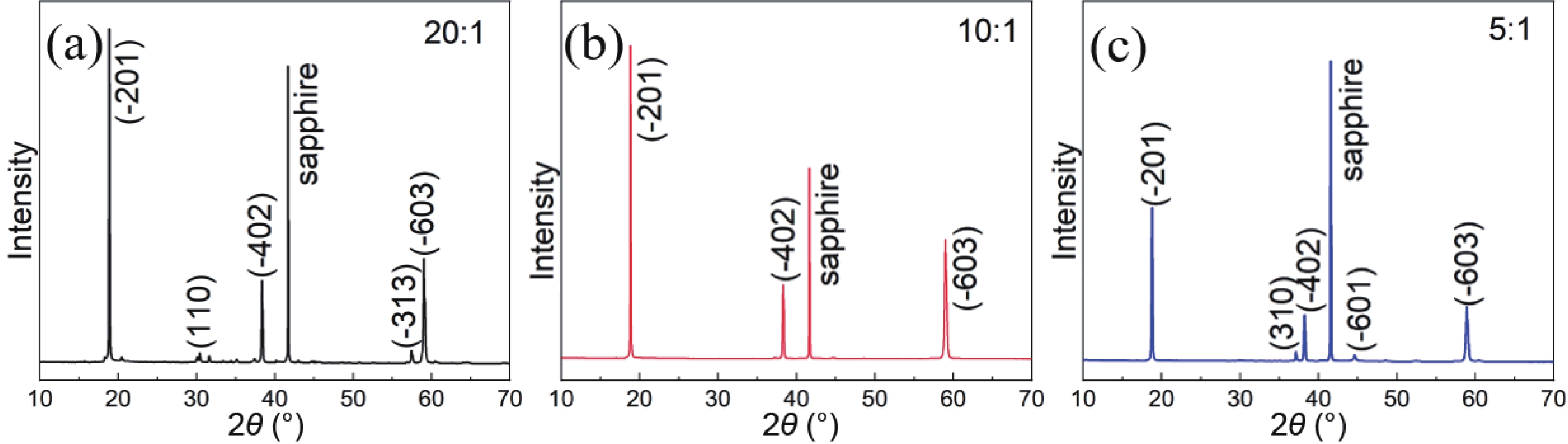
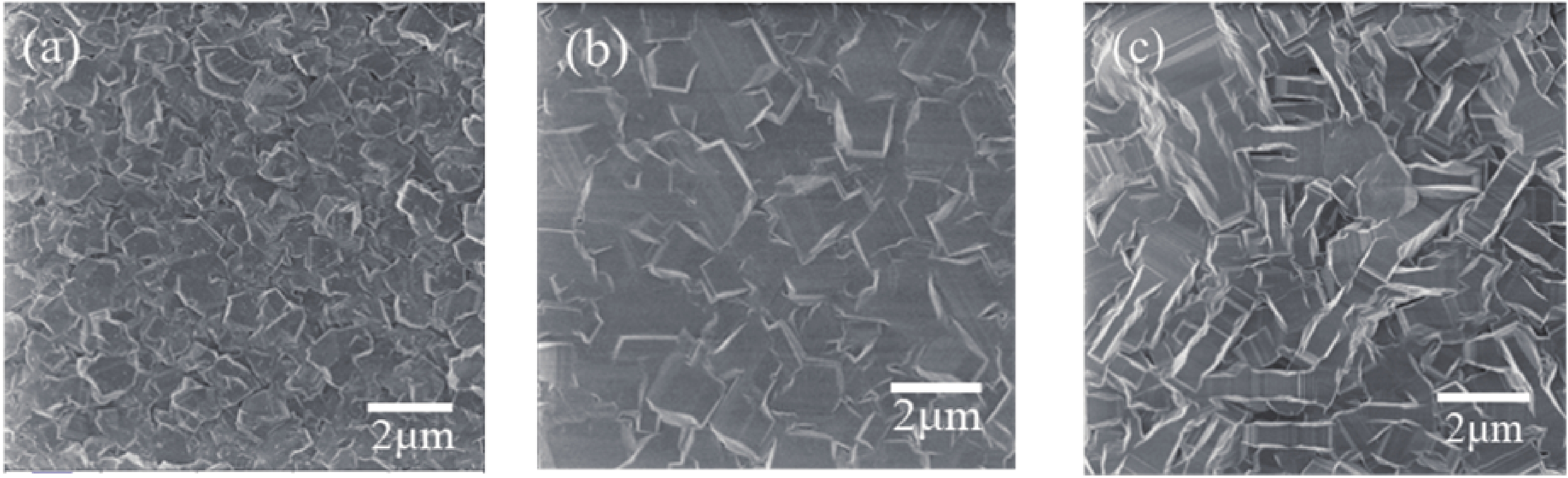
We investigated the influence of the growth temperature, O2 flow, molar ratio between Ga2O3 powder and graphite powder on the structure and morphology of the films grown on the c-plane sapphire (0001) substrates by a carbothermal reduction method. Experimental results for the heteroepitaxial growth of β-Ga2O3 illustrate that β-Ga2O3 growth by the carbothermal reduction method can be controlled. The optimal result was obtained at a growth temperature of 1050 °C. The fastest growth rate of β-Ga2O3 films was produced when the O2 flow was 20 sccm. To guarantee that β-Ga2O3 films with both high-quality crystal and morphology properties, the ideal molar ratio between graphite powder and Ga2O3 powder should be set at 10 : 1.
J. Semicond.
2023, 44(6): 062805 doi: 10.1088/1674-4926/44/6/062805
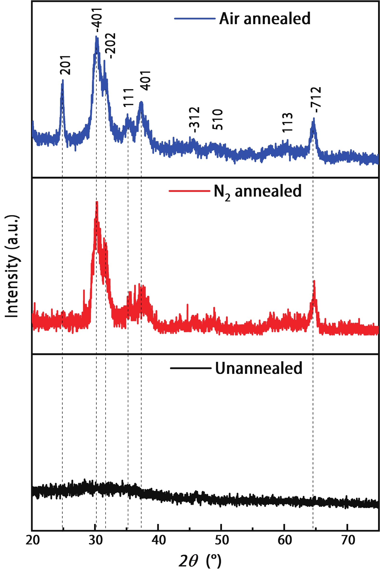
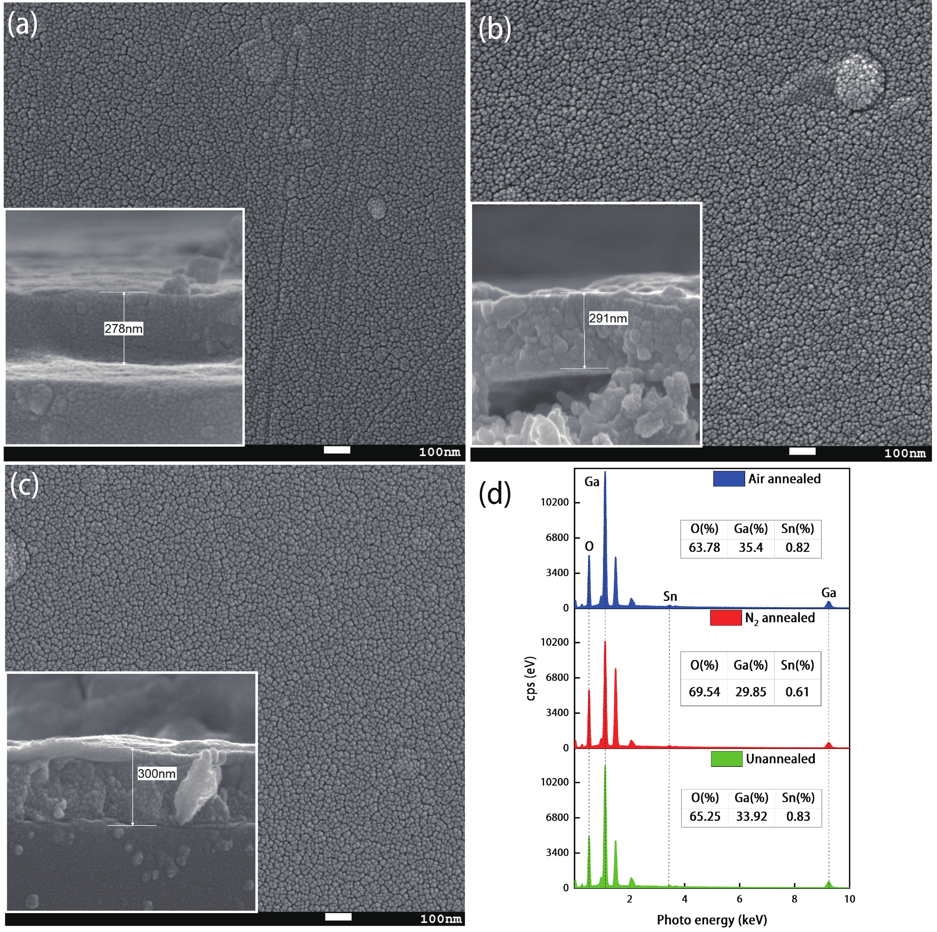
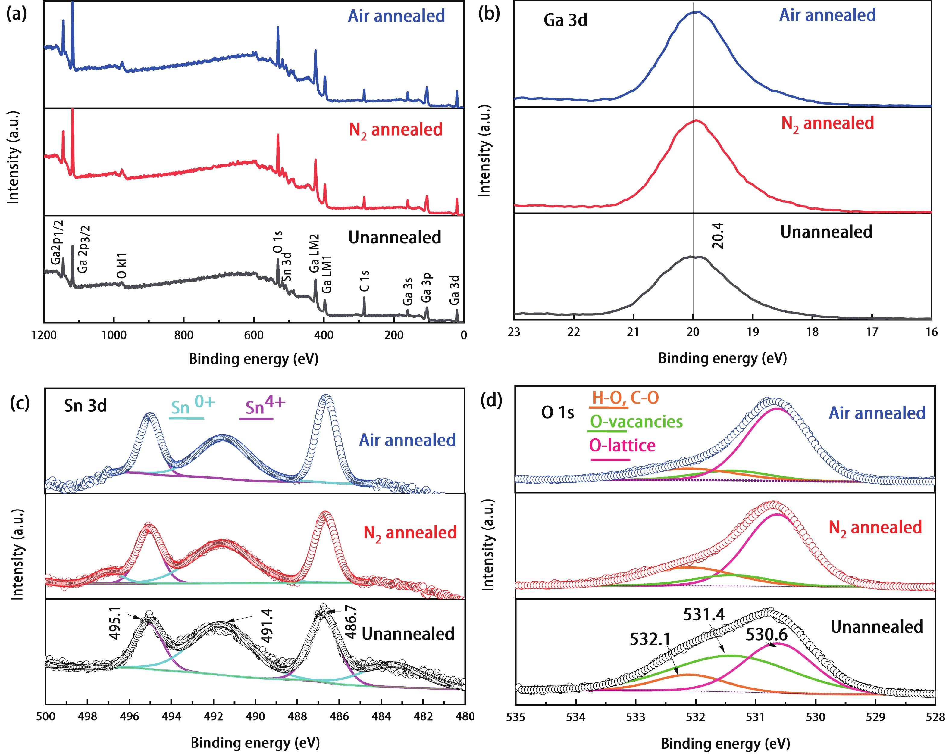
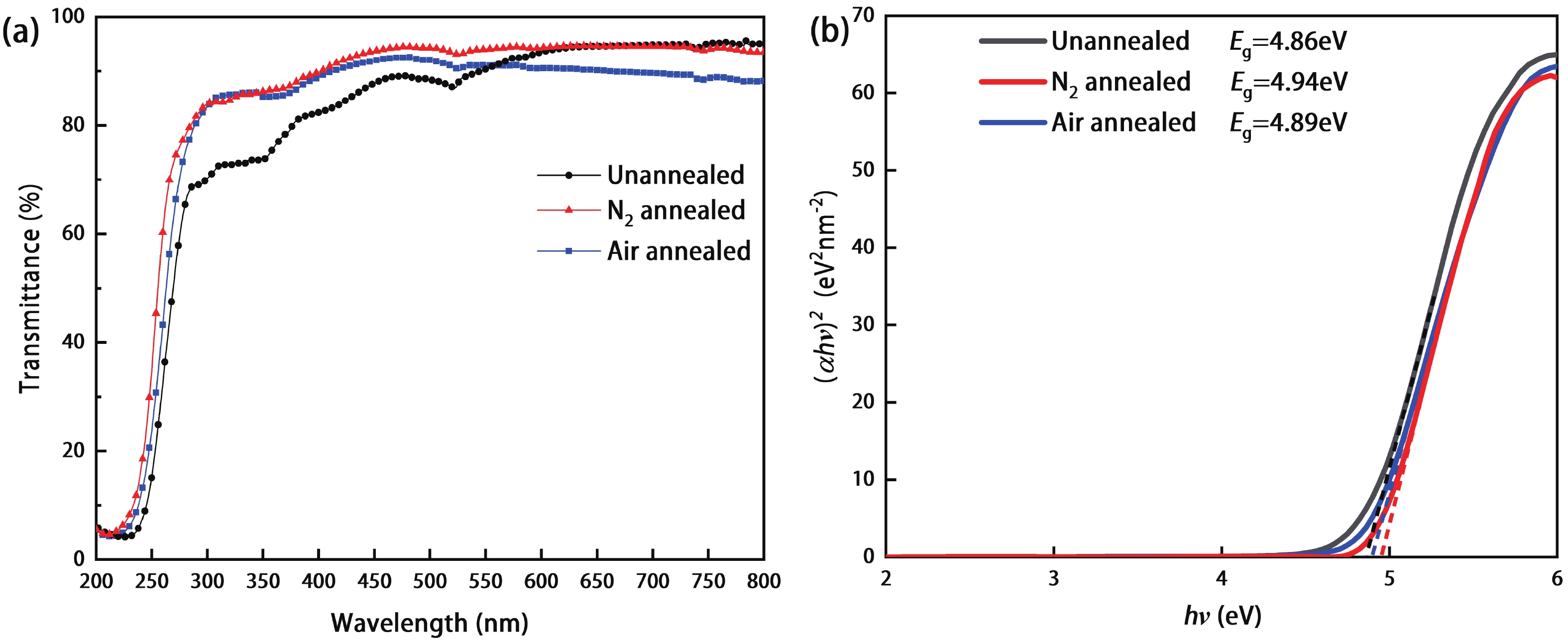
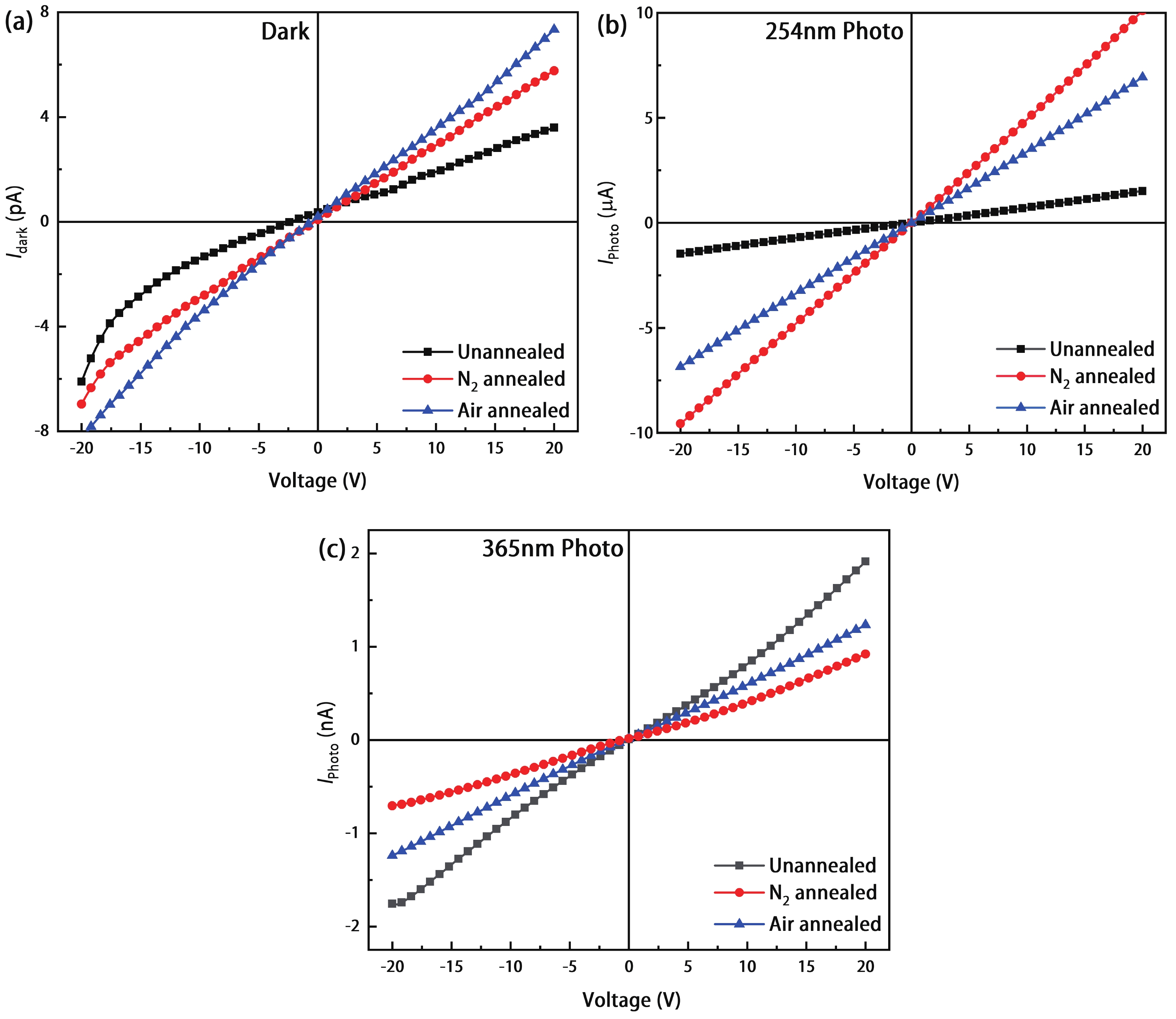
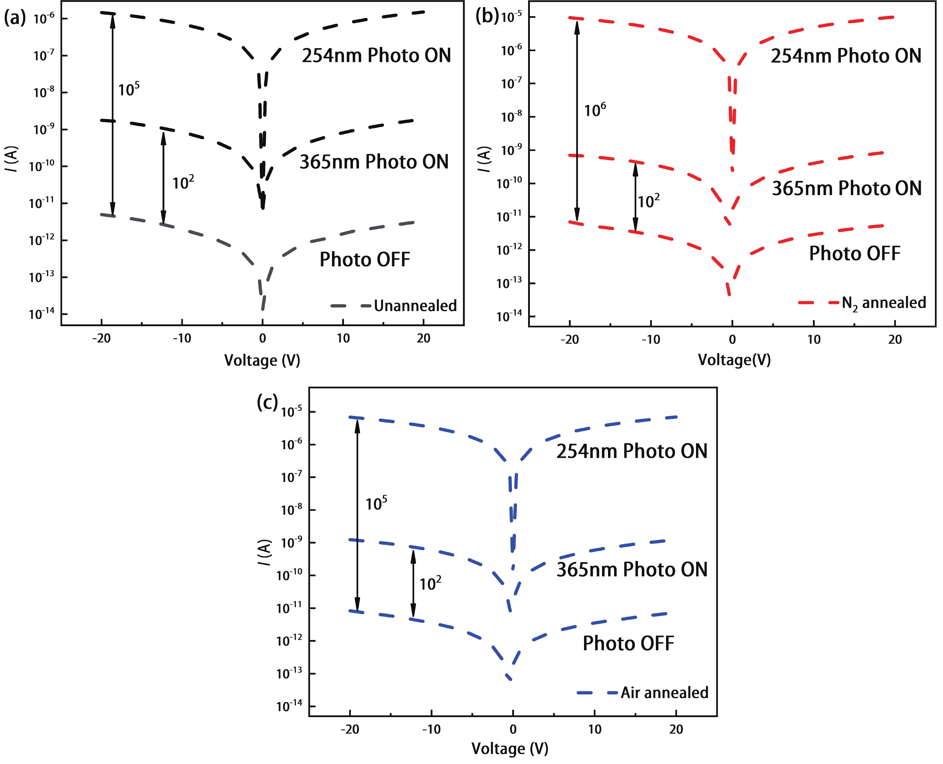
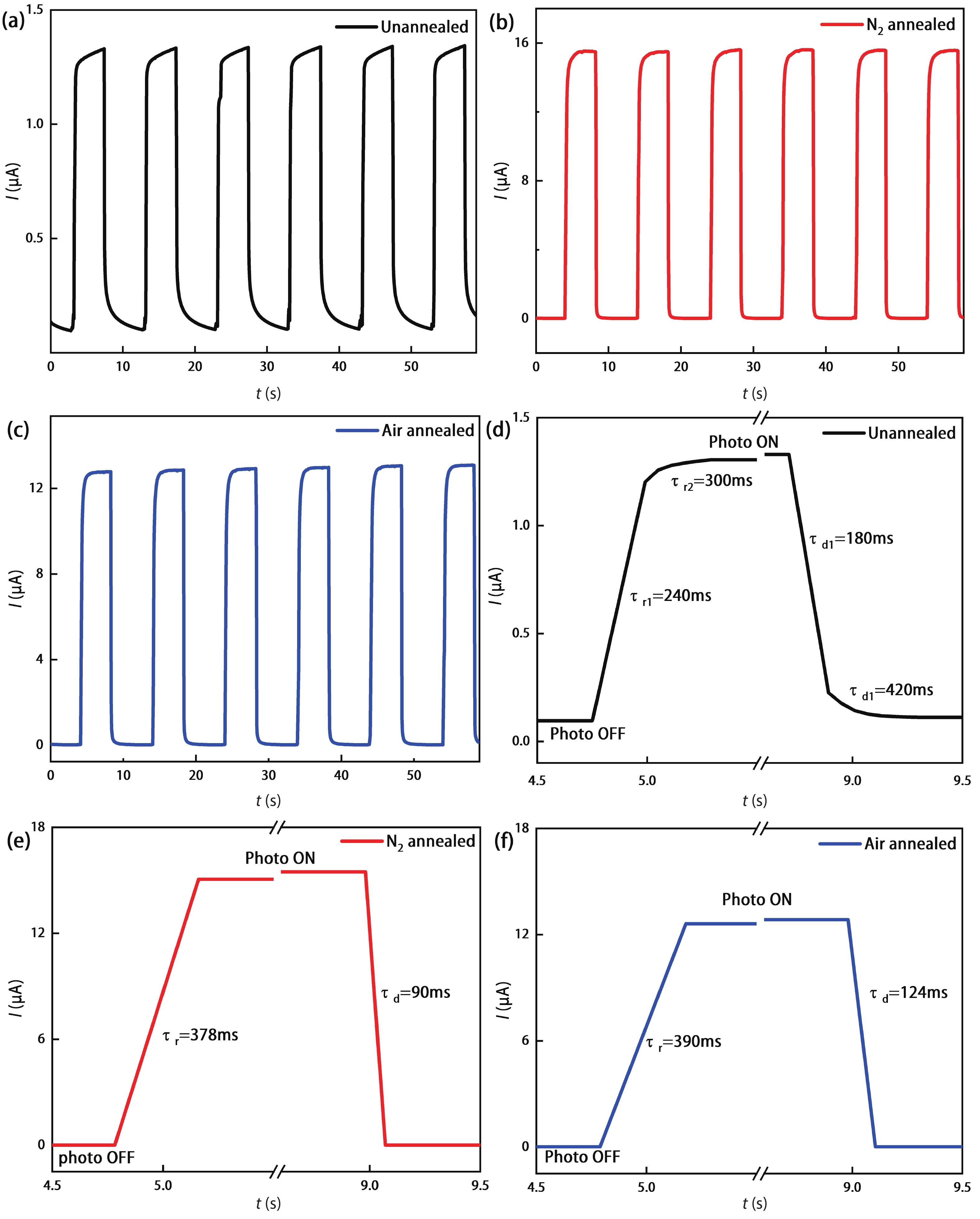
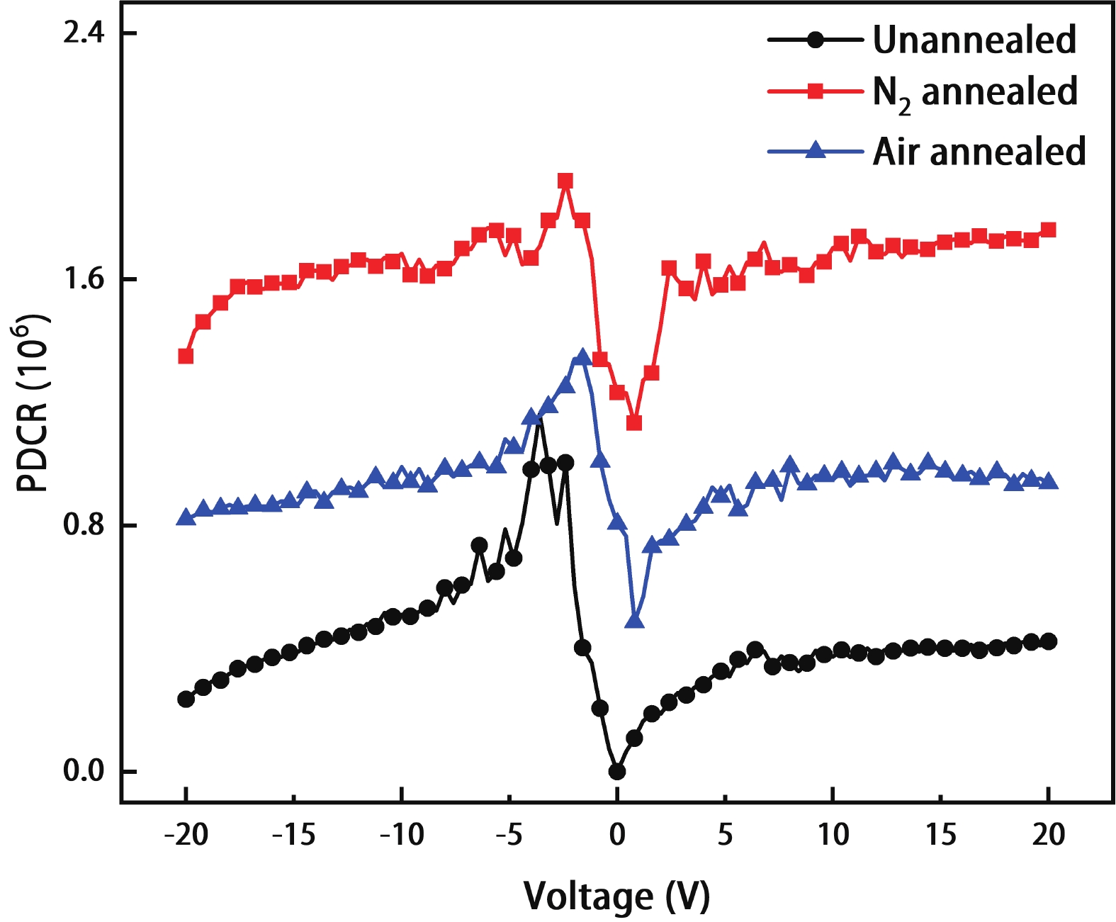
Sn doping is an effective way to improve the response rate of Ga2O3 film based solar-blind detectors. In this paper, Sn-doped Ga2O3 films were prepared on a sapphire substrate by radio frequency magnetron sputtering. The films were characterized by X-ray diffraction, scanning electron microscopy, X-ray photoelectron spectroscopy and ultraviolet visible spectroscopy, and the effect of annealing atmosphere on the properties of films was studied. The Ga2O3 films changed from amorphous to β-Ga2O3 after annealing at 900 °C. The films were composed of micro crystalline particles with a diameter of about 5–20 nm. The β-Ga2O3 had high transmittance for wavelengths above 300 nm, and obvious absorption for solar-blind signals at 200–280 nm. The metal semiconductor metal type solar-blind detectors were prepared. The detector based on Sn-doped β-Ga2O3 thin film annealed in N2 has the best response performance to 254 nm light. The photo-current is 10 μA at 20 V, the dark-current is 5.76 pA, the photo dark current ratio is 1.7 × 10⁶, the response rate is 12.47 A/W, the external quantum efficiency is 6.09 × 10³%, the specific detection rate is 2.61 × 10¹² Jones, the response time and recovery time are 378 and 90 ms, respectively.
J. Semicond.
2023, 44(6): 062806 doi: 10.1088/1674-4926/44/6/062806

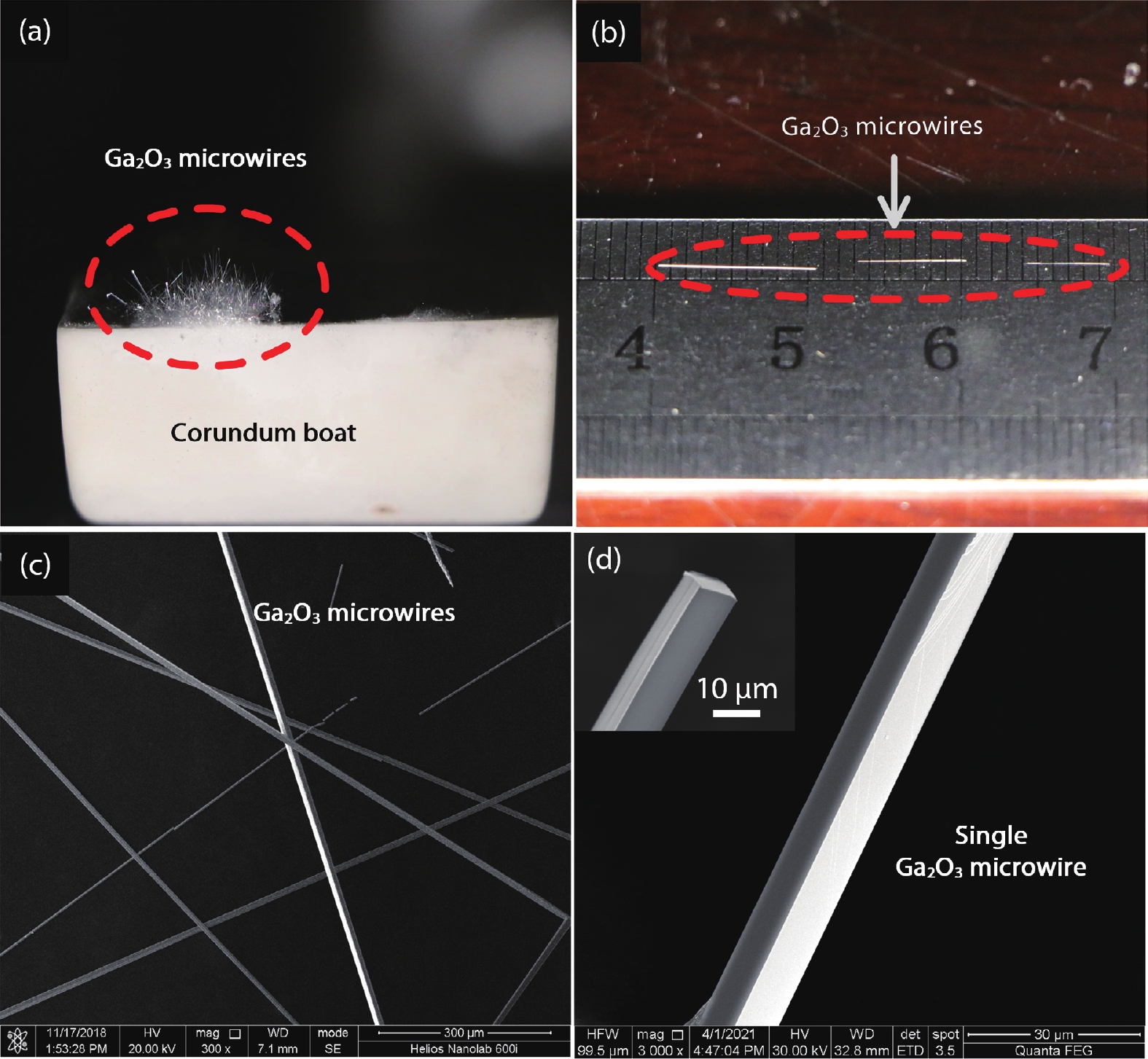
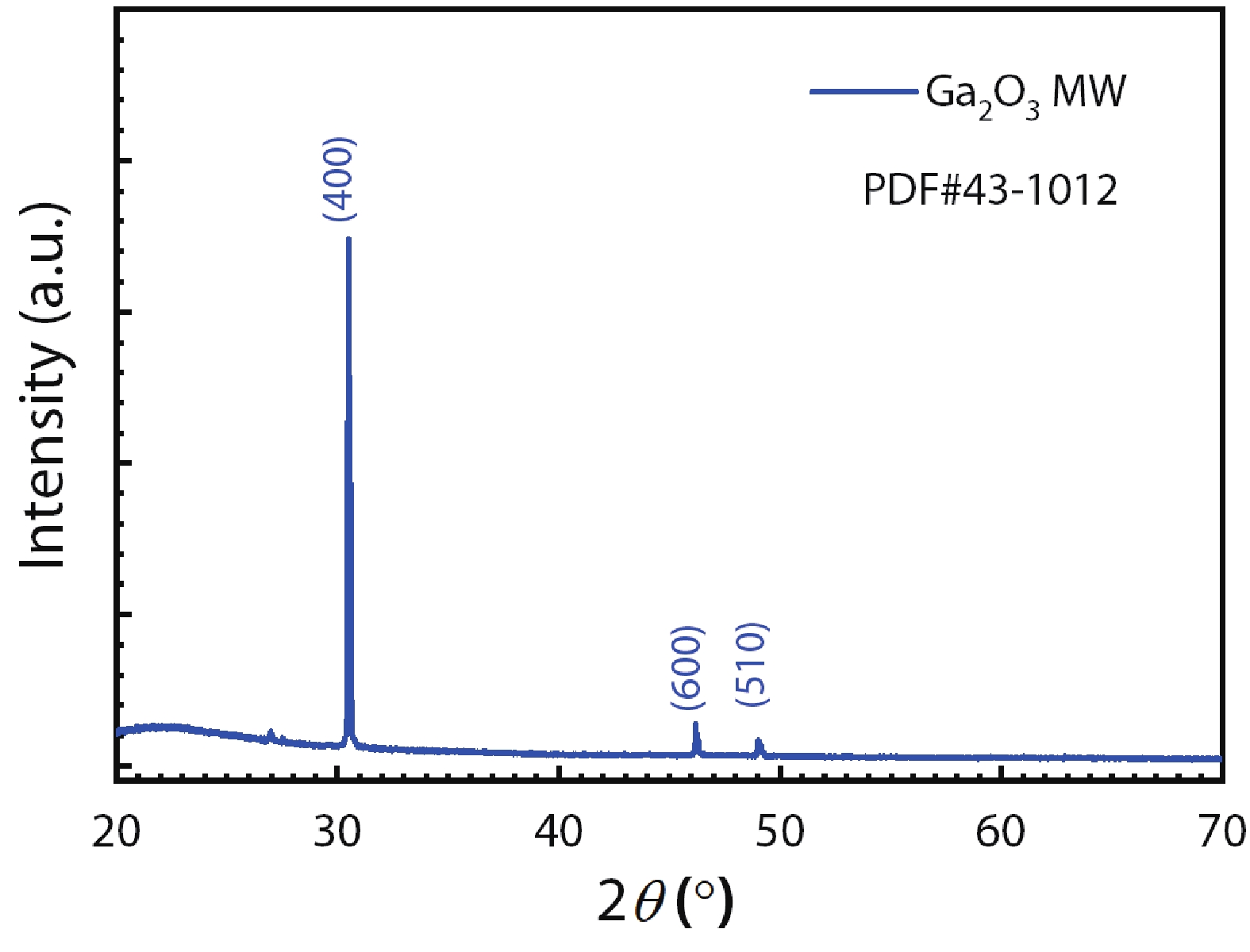
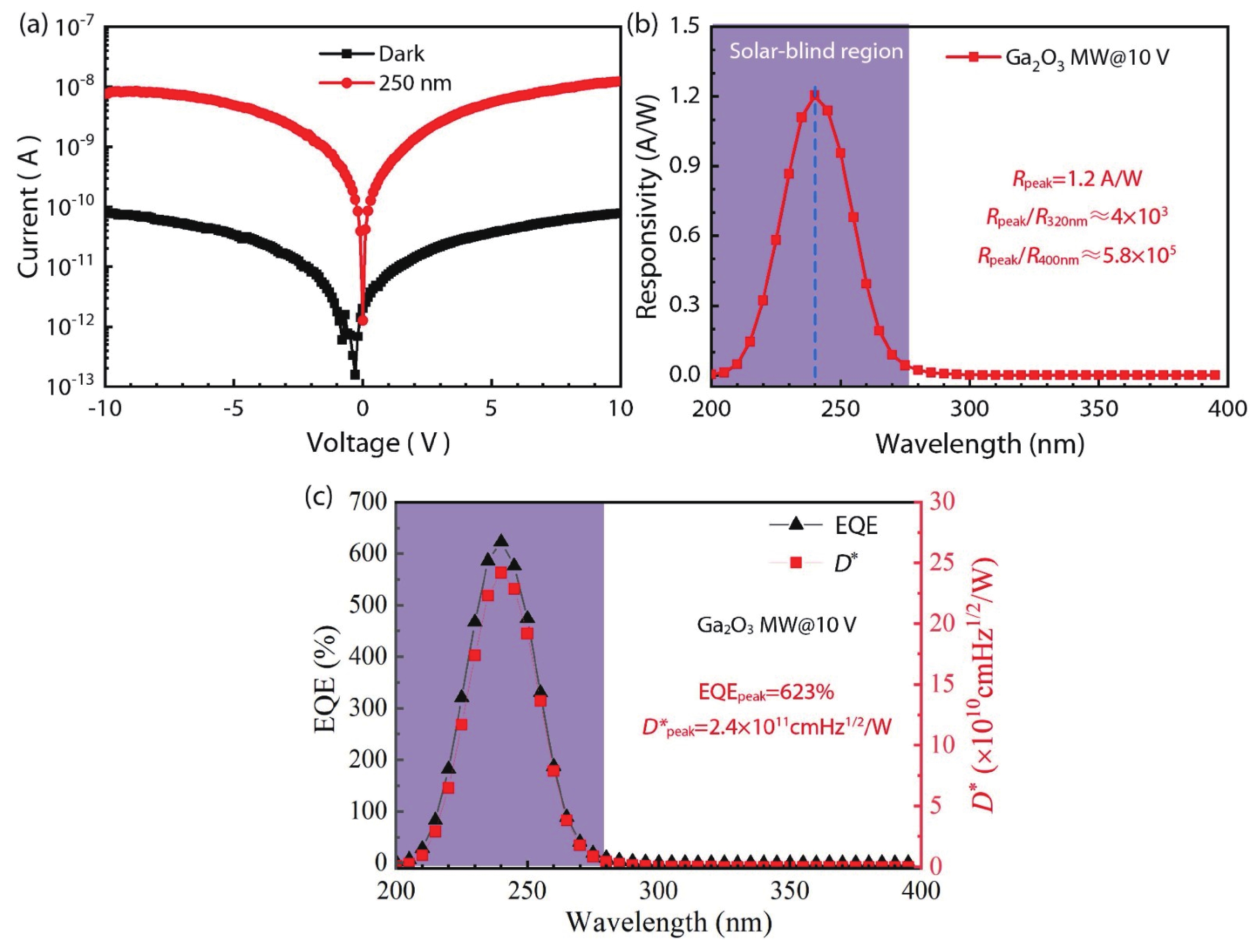
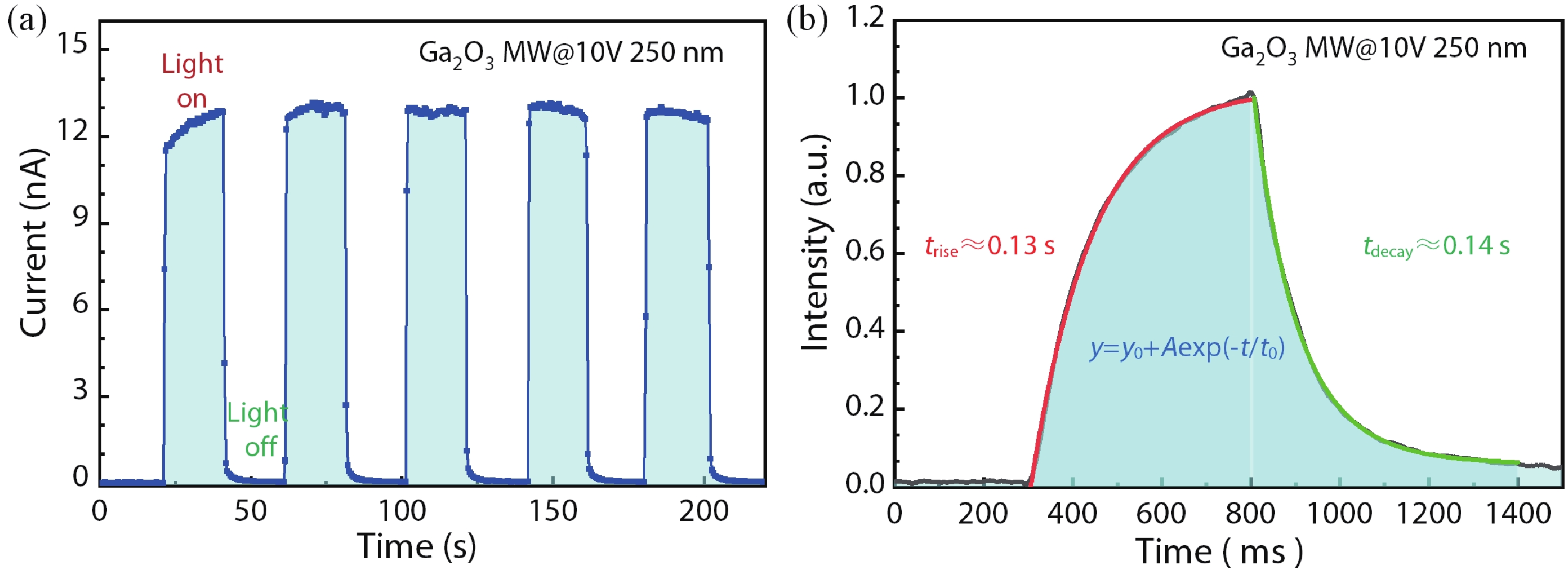
Ultrawide band gap semiconductors are promising solar-blind ultraviolet (UV) photodetector materials due to their suitable bandgap, strong absorption and high sensitivity. Here, β-Ga2O3 microwires with high crystal quality and large size were grown by the chemical vapor deposition (CVD) method. The microwires reach up to 1 cm in length and were single crystalline with low defect density. Owing to its high crystal quality, a metal–semiconductor–metal photodetector fabricated from a Ga2O3 microwire showed a responsivity of 1.2 A/W at 240 nm with an ultrahigh UV/visible rejection ratio (Rpeak/R400 nm) of 5.8 × 10⁵, indicating that the device has excellent spectral selectivity. In addition, no obvious persistent photoconductivity was observed in the test. The rise and decay time constants of the device were 0.13 and 0.14 s, respectively. This work not only provides a growth method for high-quality Ga2O3 microwires, but also demonstrates the excellent performance of Ga2O3 microwires in solar-blind ultraviolet detection.