Issue Browser
Volume 44, Issue 5,
May 2023
Column


J. Semicond.
2023, 44(5): 053101 doi: 10.1088/1674-4926/44/5/053101
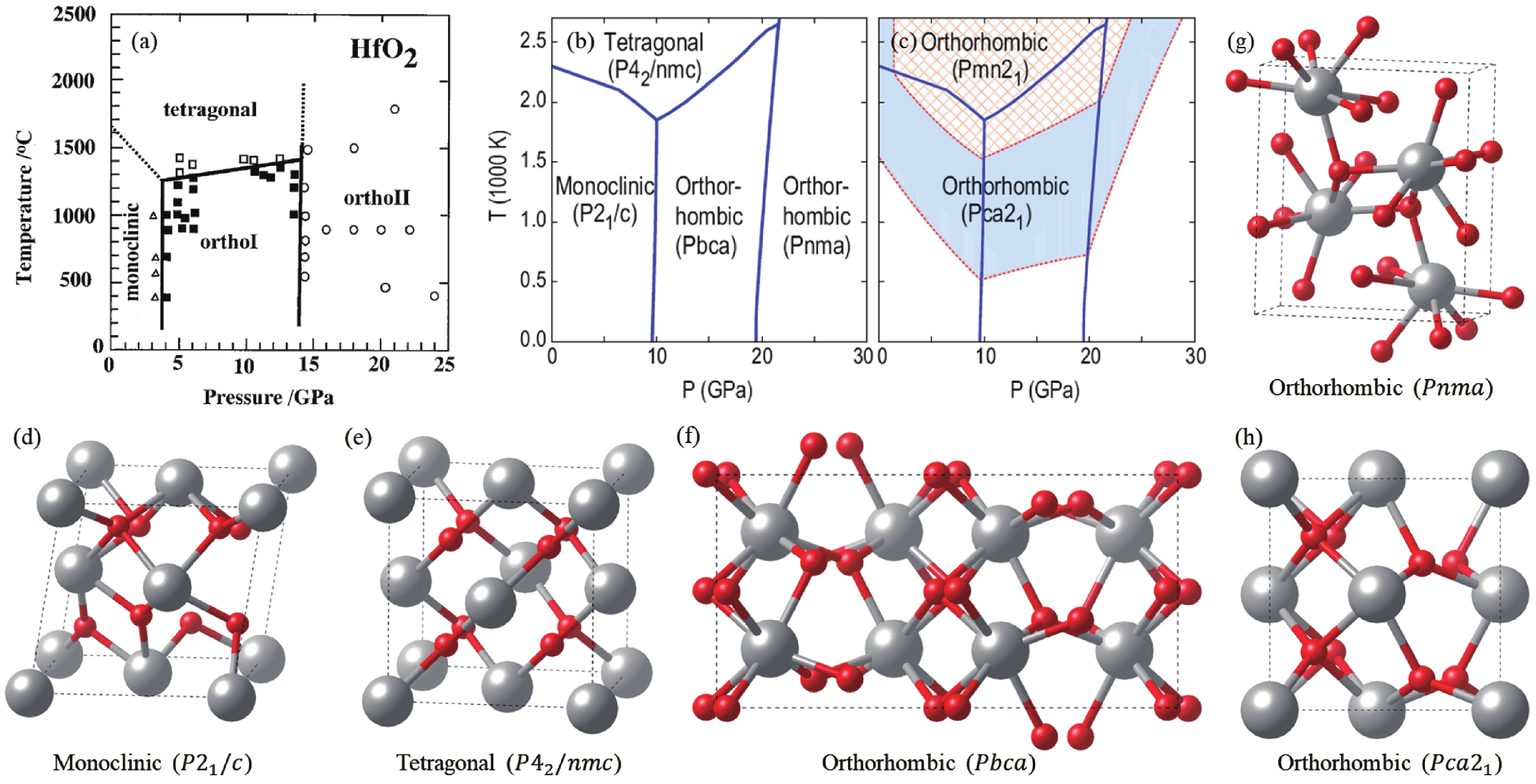
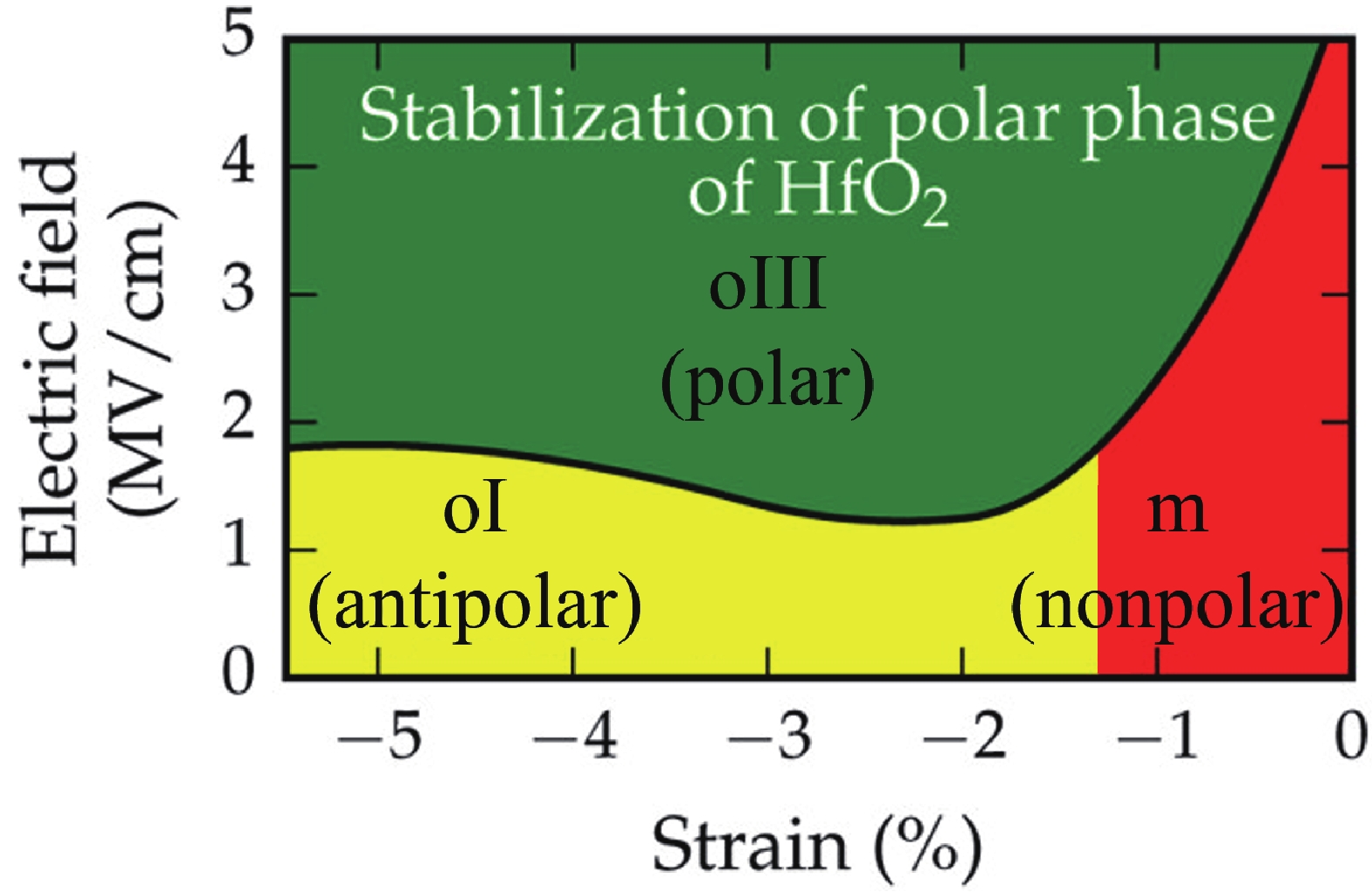
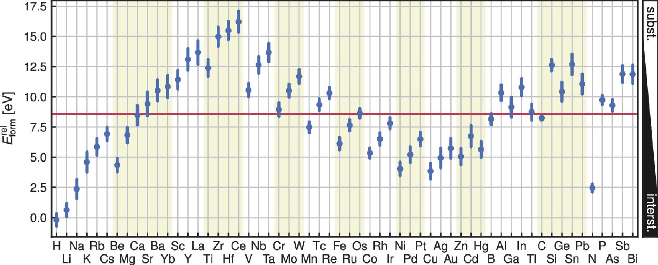
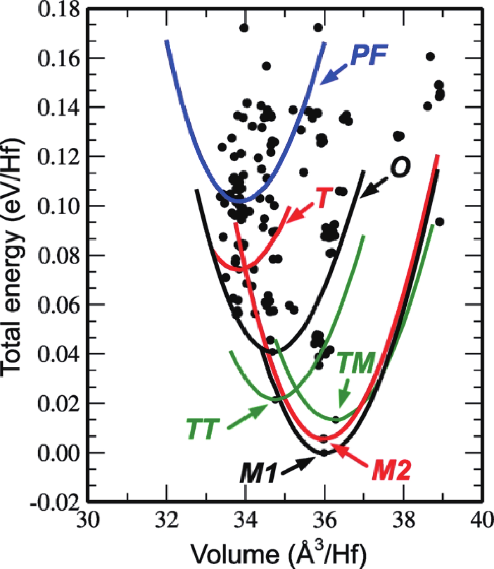
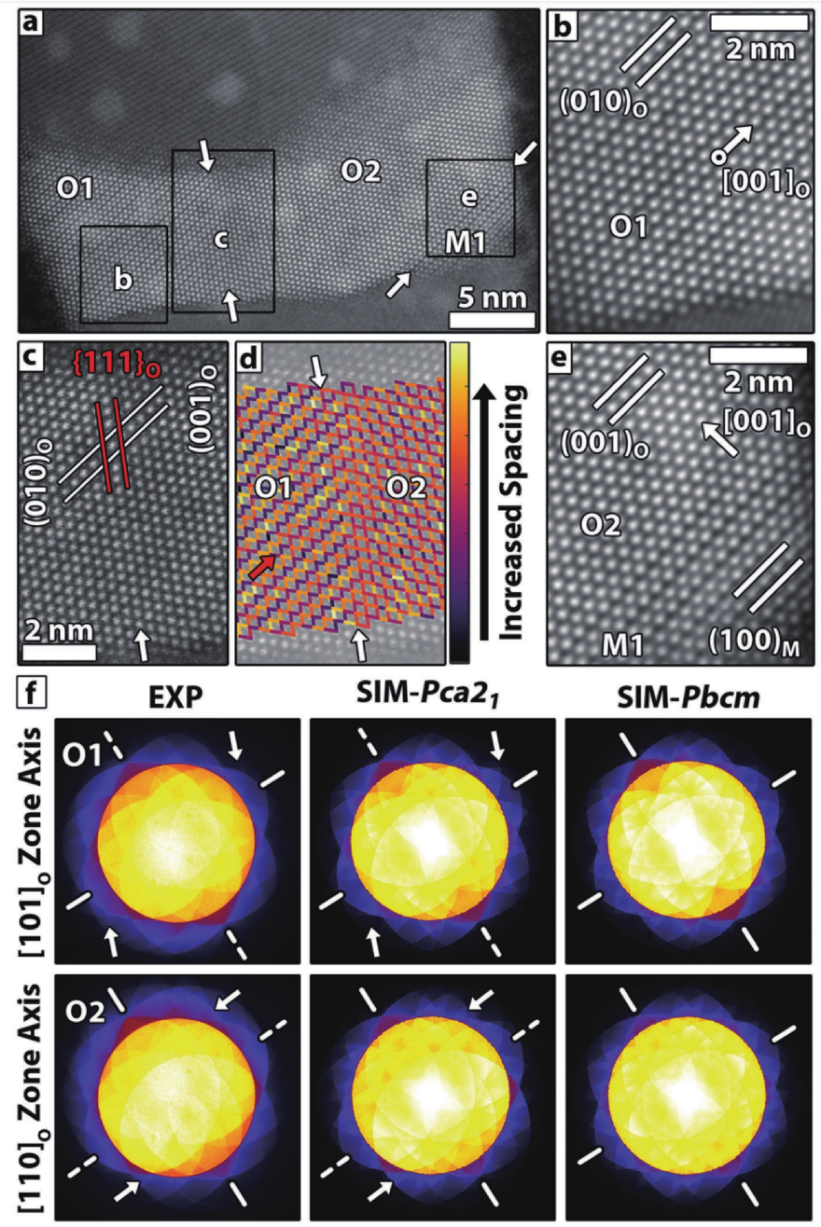
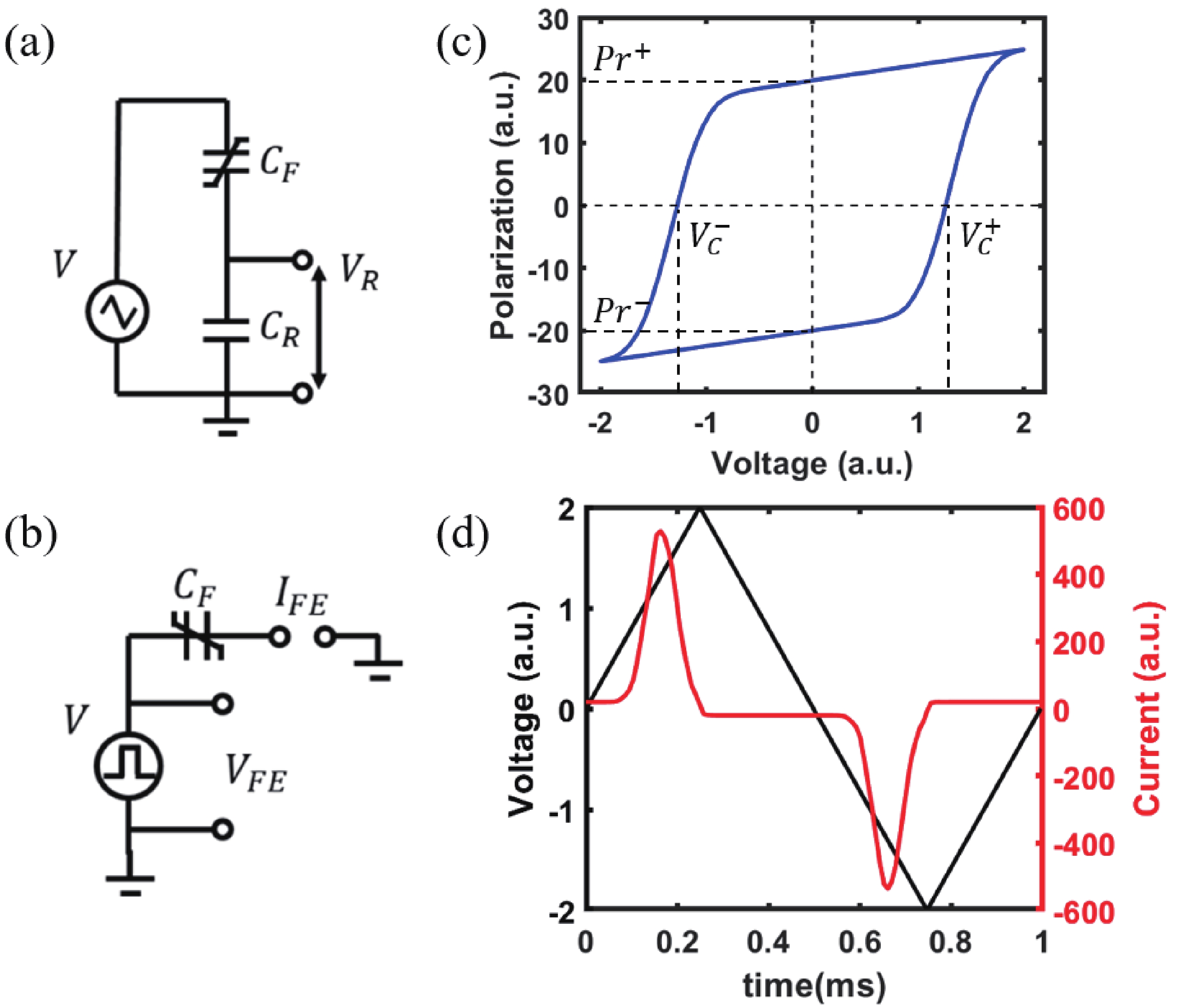
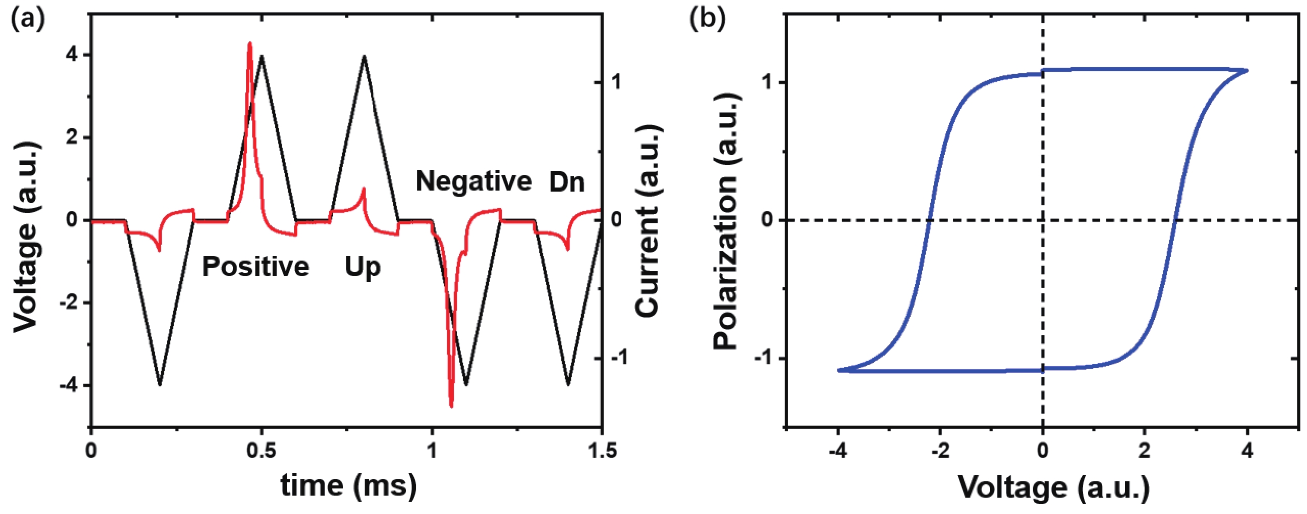
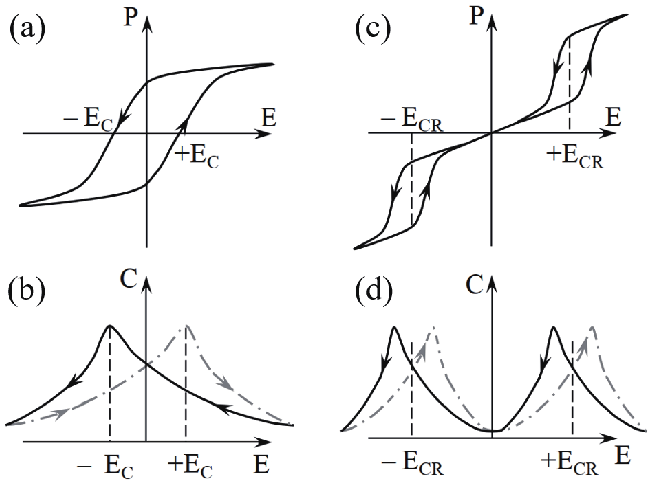
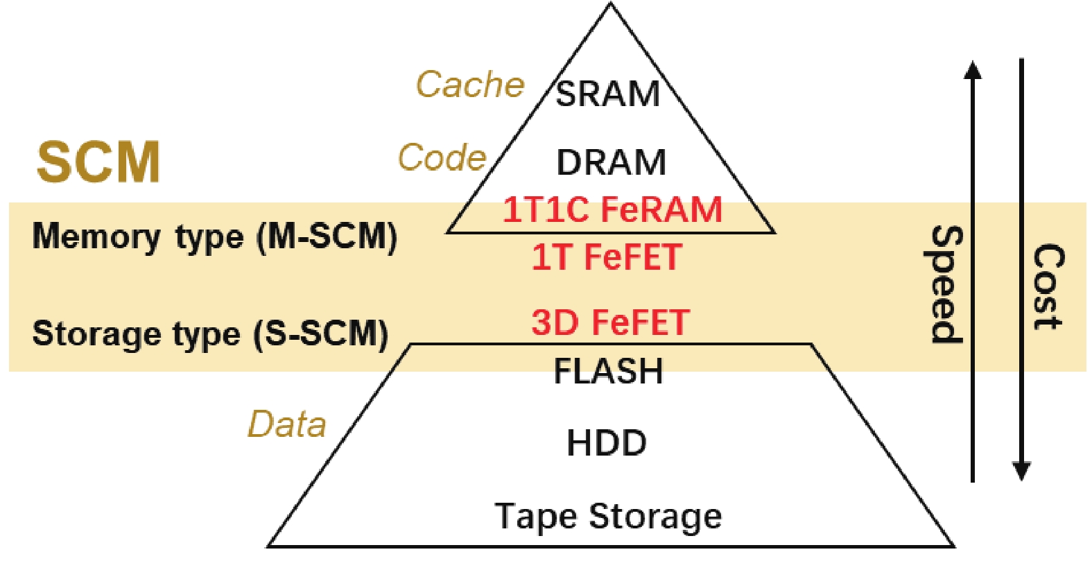
The finding of the robust ferroelectricity in HfO2-based thin films is fantastic from the view point of both the fundamentals and the applications. In this review article, the current research status of the future prospects for the ferroelectric HfO2-based thin films and devices are presented from fundamentals to applications. The related issues are discussed, which include: 1) The ferroelectric characteristics observed in HfO2-based films and devices associated with the factors of dopant, strain, interface, thickness, defect, fabrication condition, and more; 2) physical understanding on the observed ferroelectric behaviors by the density functional theory (DFT)-based theory calculations; 3) the characterizations of microscopic and macroscopic features by transmission electron microscopes-based and electrical properties-based techniques; 4) modeling and simulations, 5) the performance optimizations, and 6) the applications of some ferroelectric-based devices such as ferroelectric random access memory, ferroelectric-based field effect transistors, and the ferroelectric tunnel junction for the novel information processing systems.


J. Semicond.
2023, 44(5): 053102 doi: 10.1088/1674-4926/44/5/053102
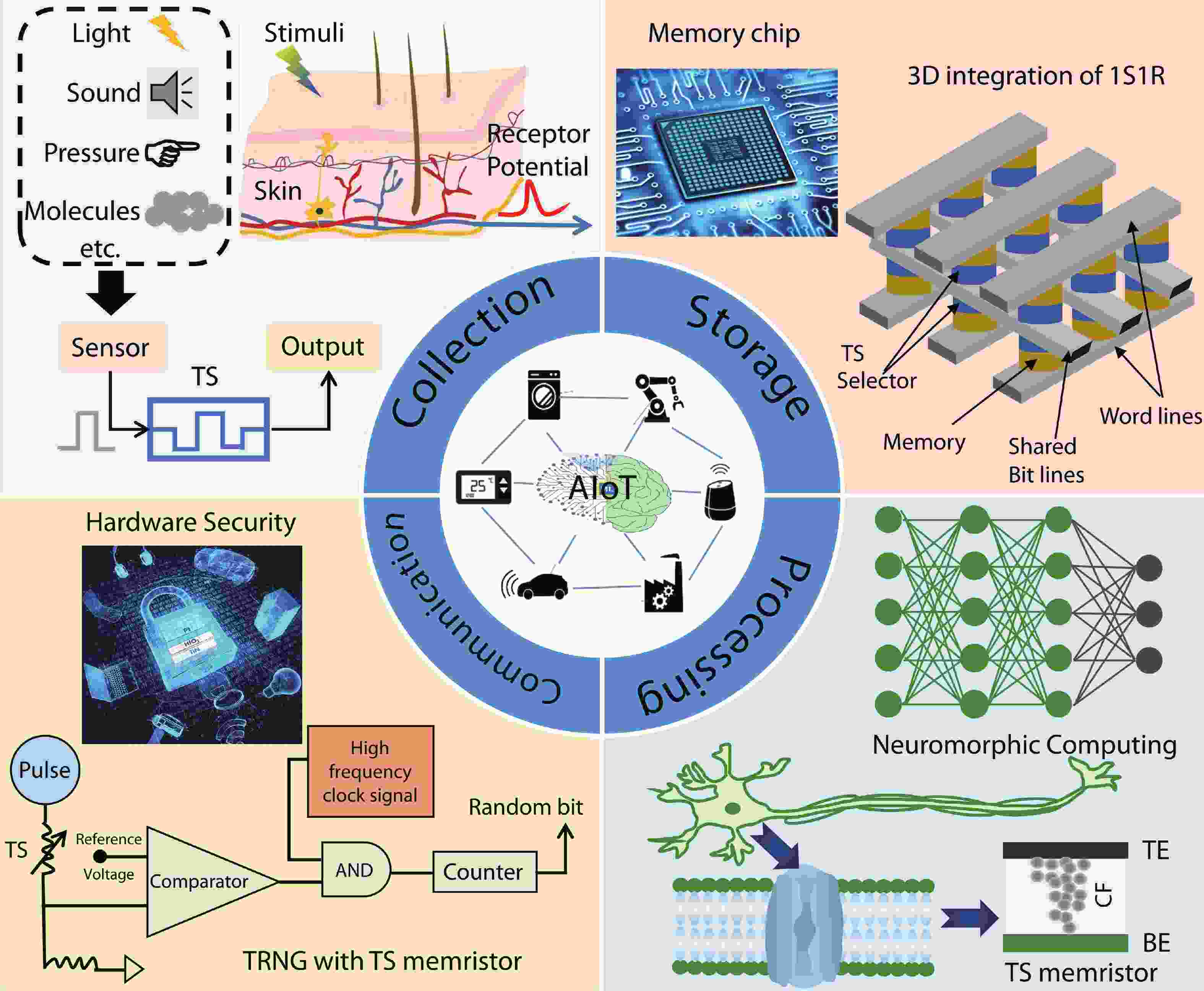
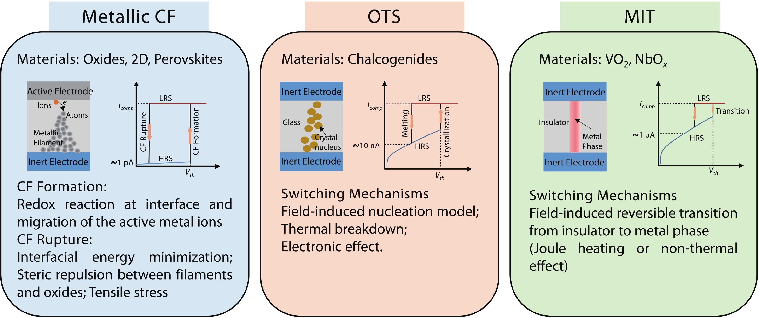
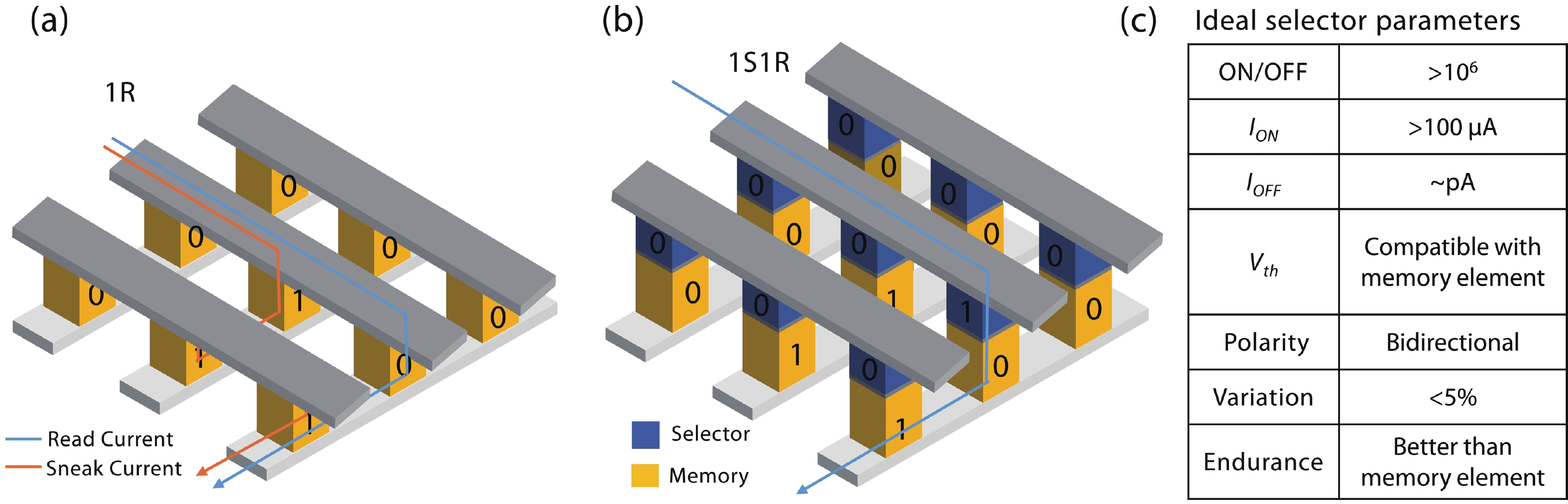
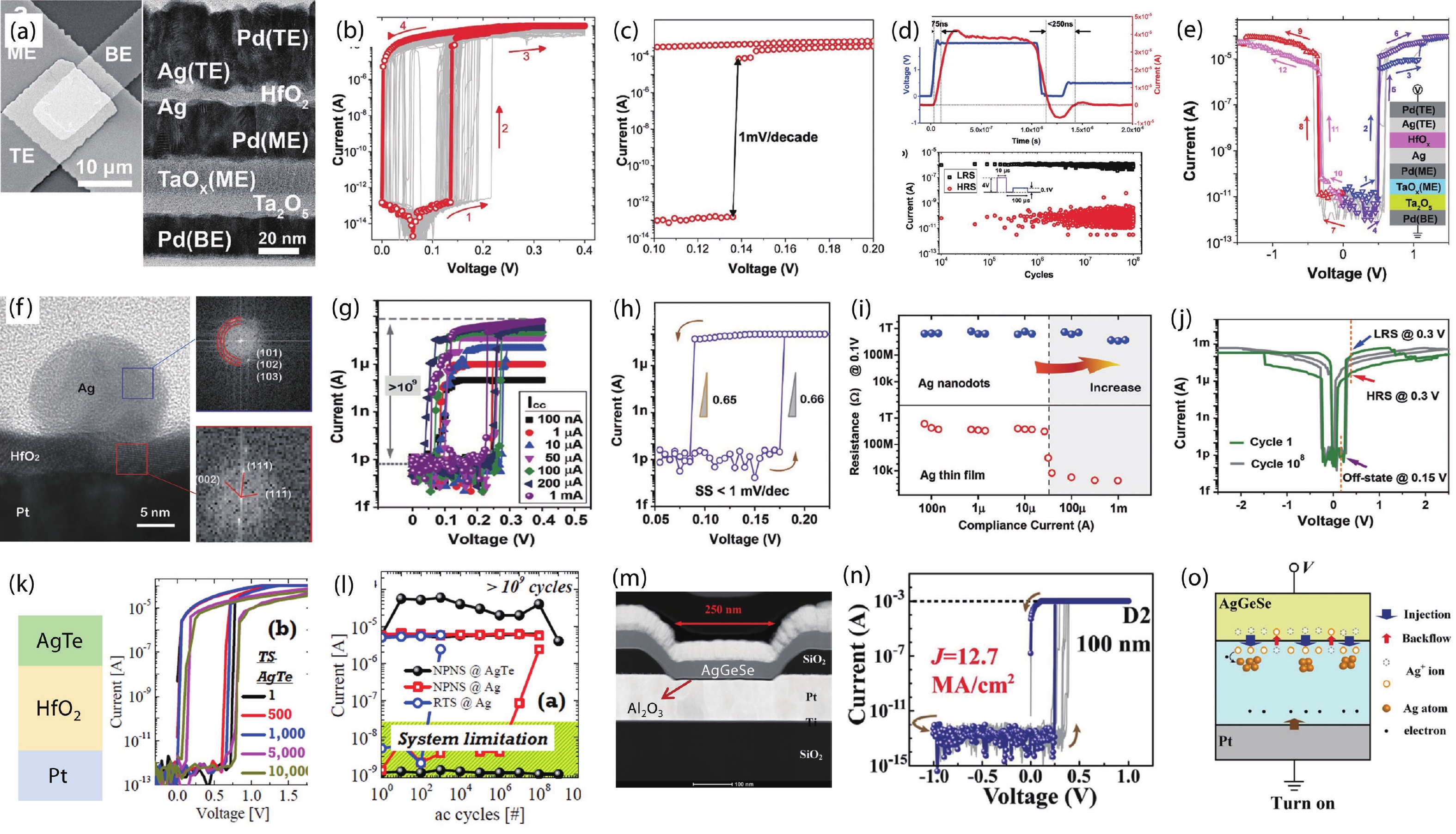
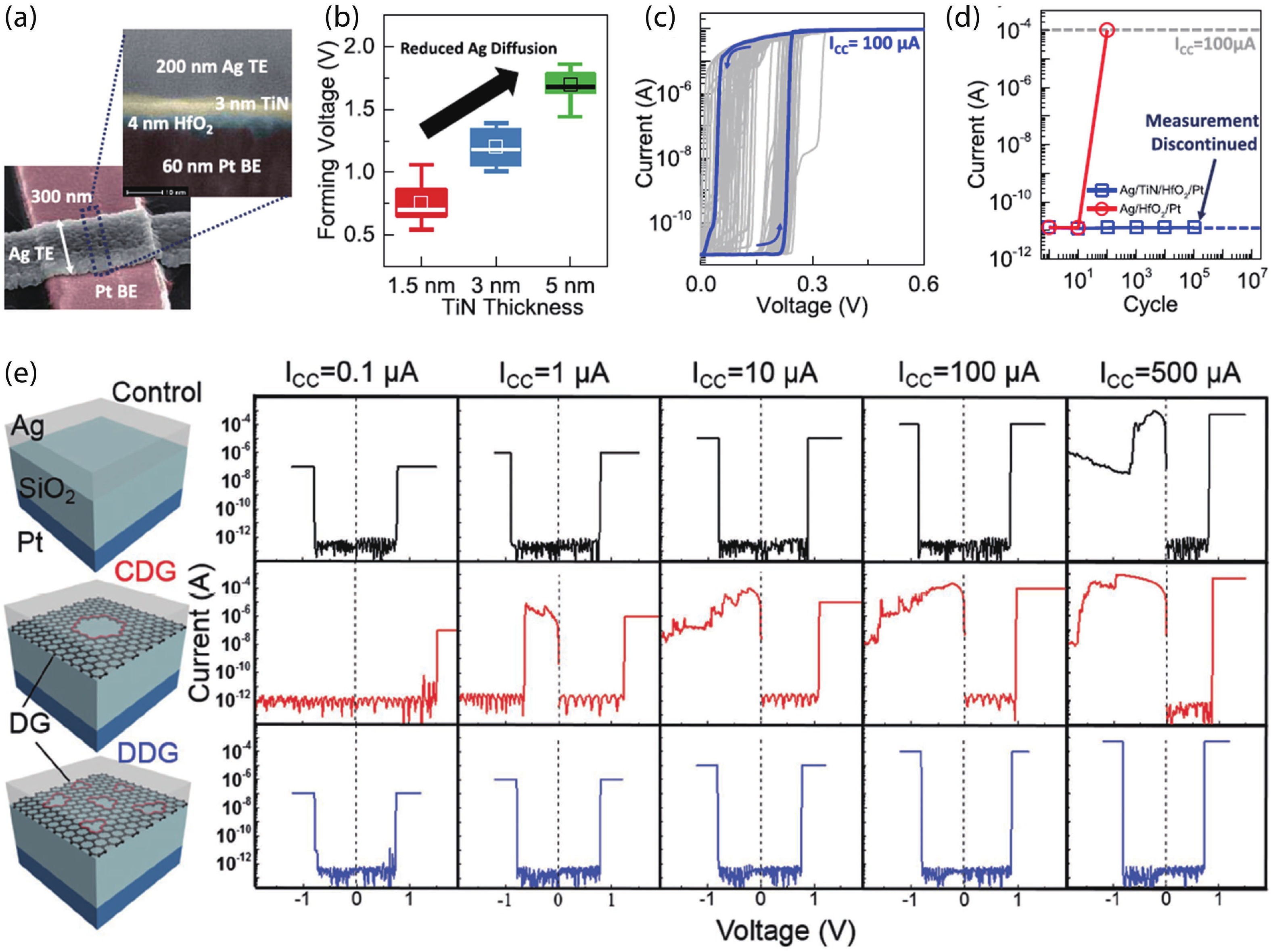
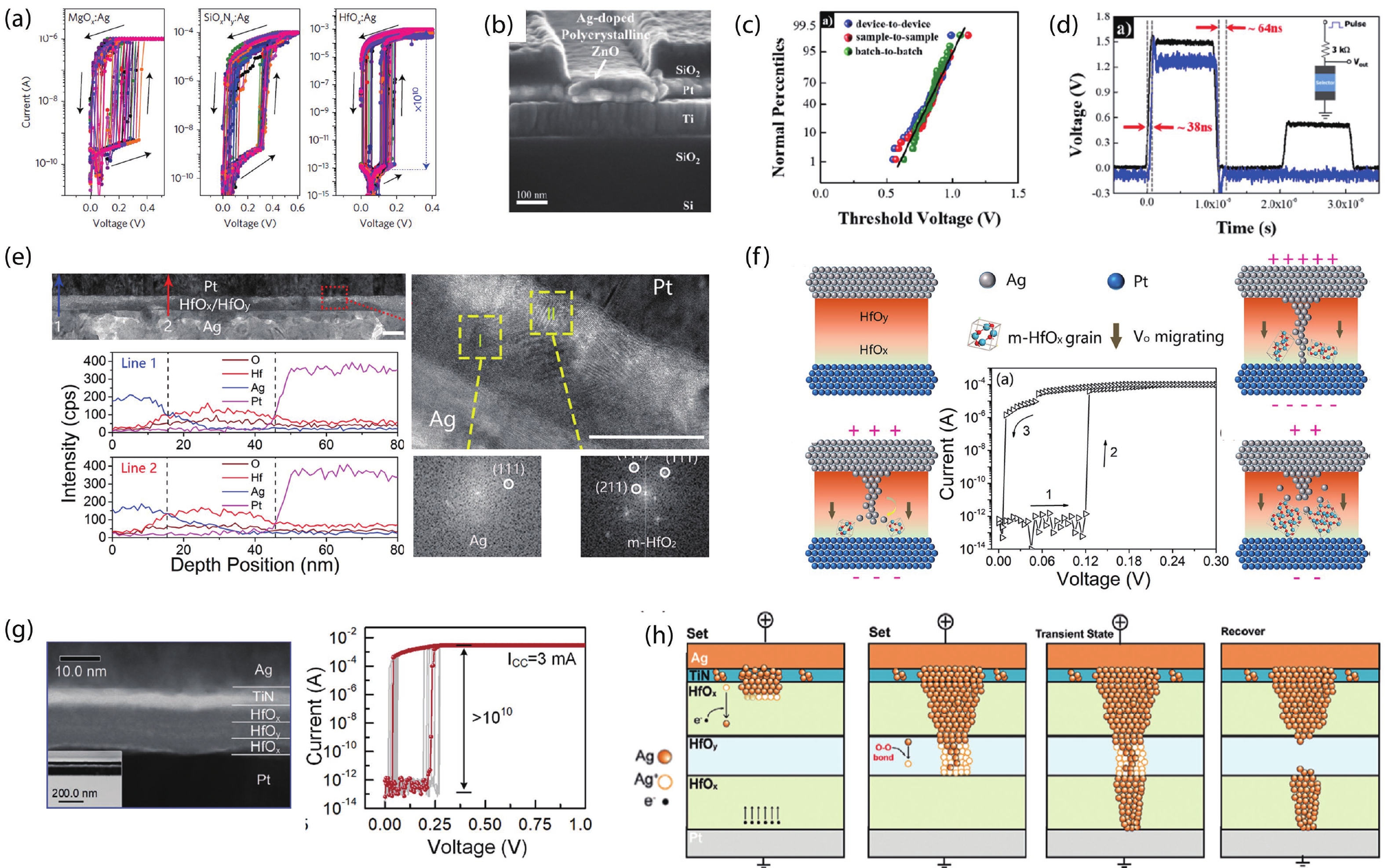
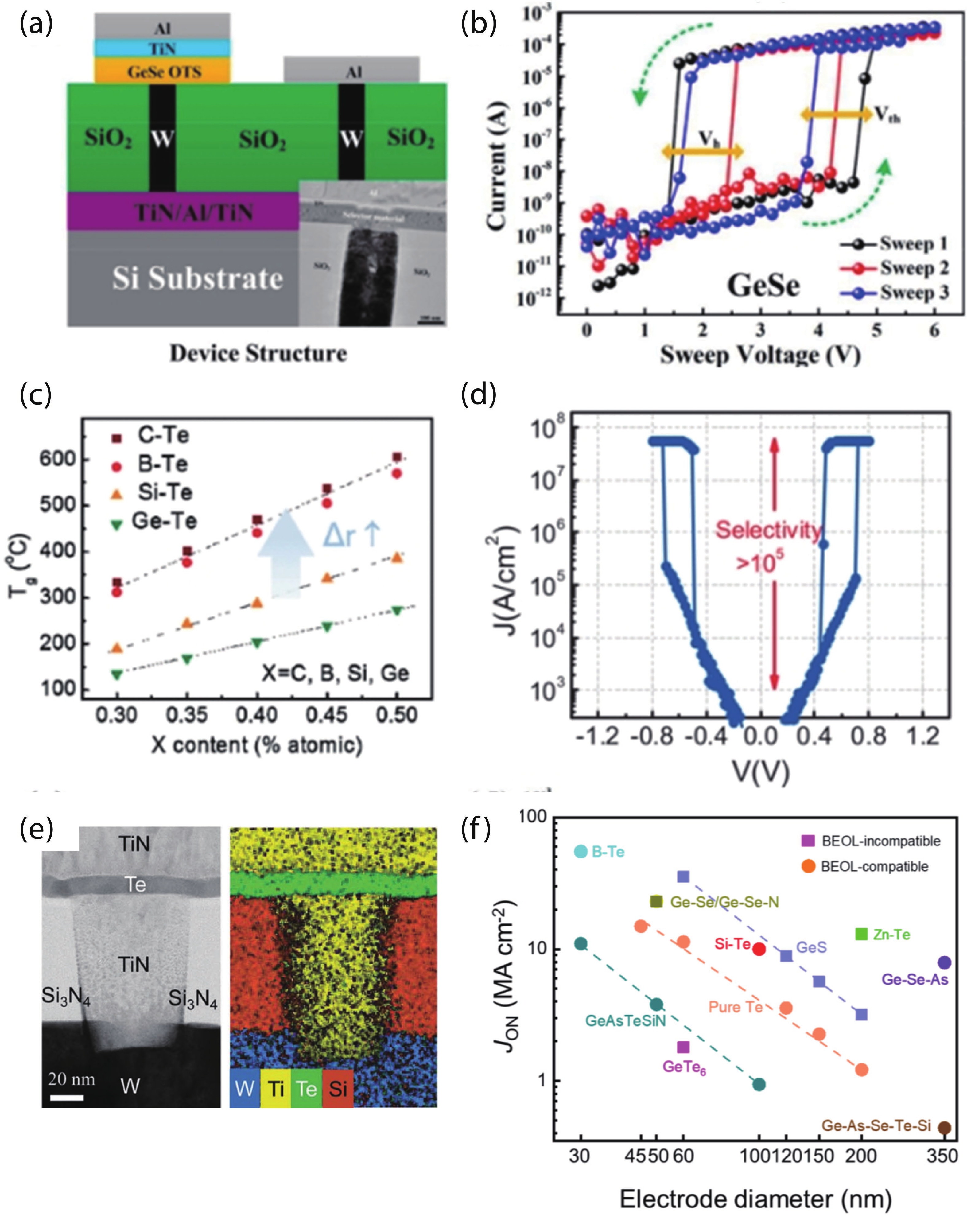
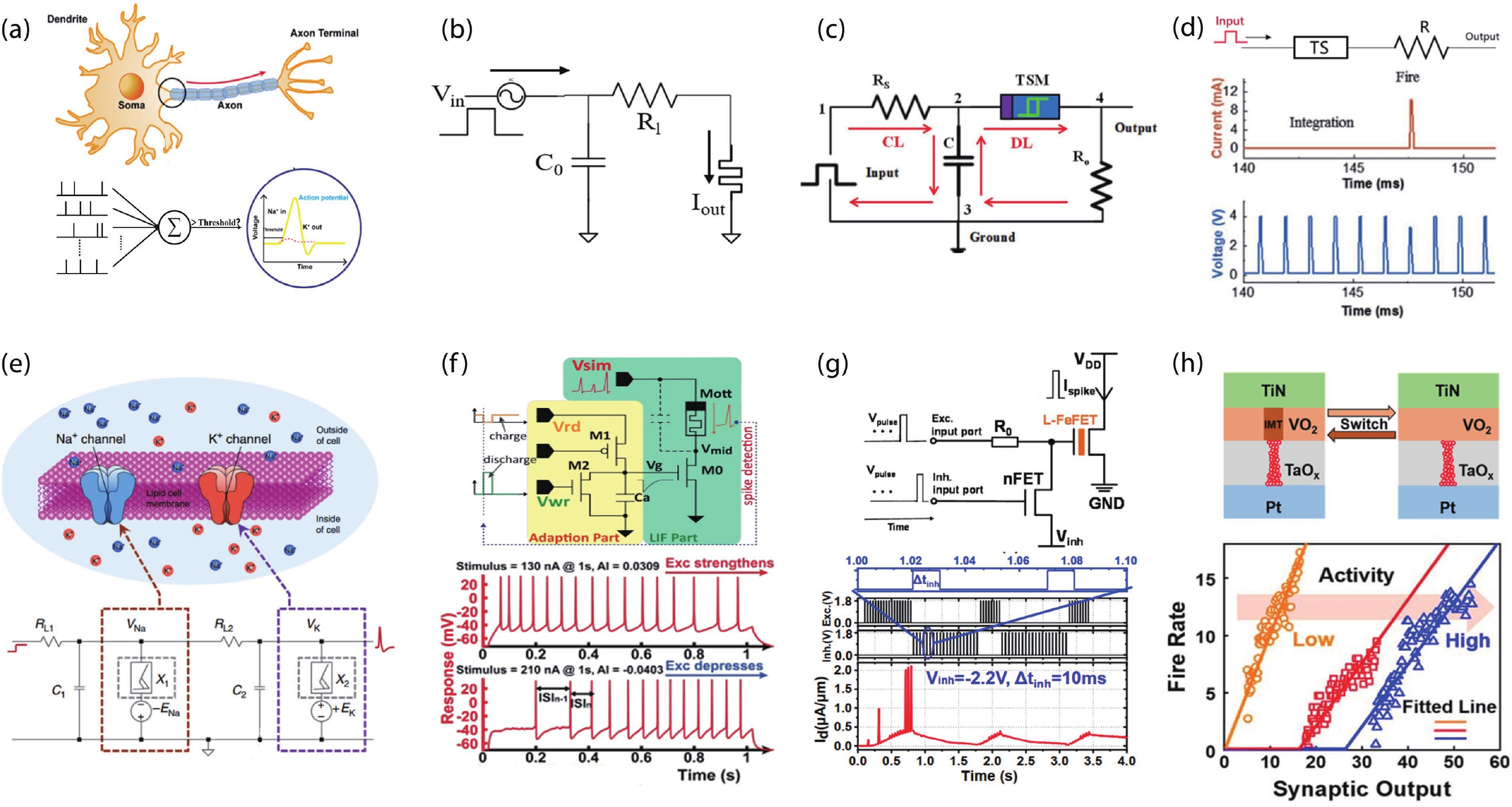
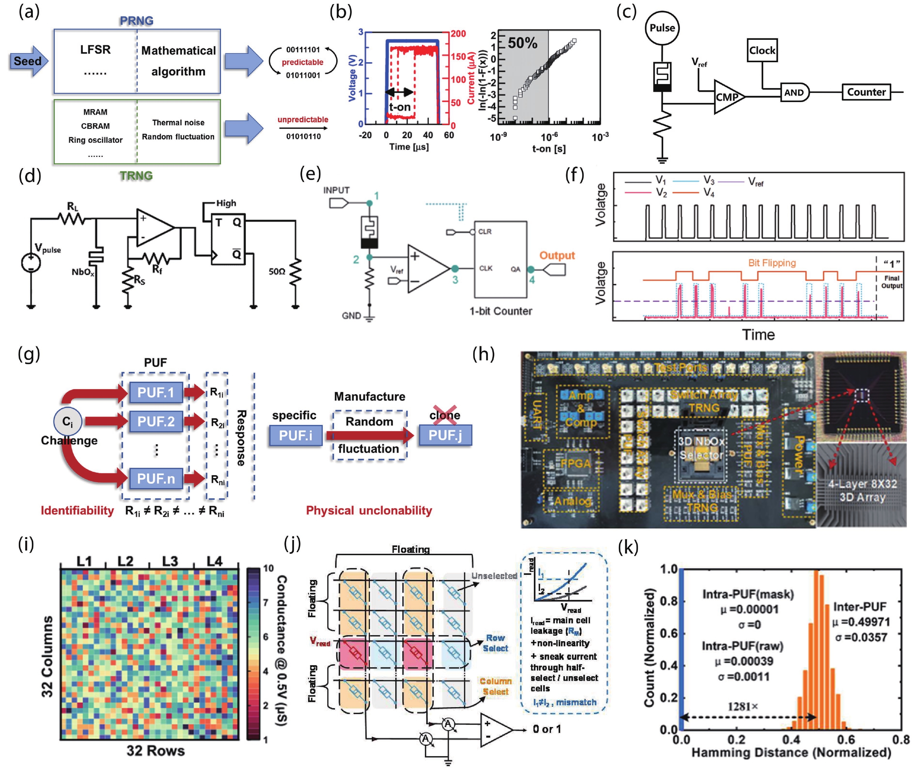
With rapid advancement and deep integration of artificial intelligence and the internet-of-things, artificial intelligence of things has emerged as a promising technology changing people’s daily life. Massive growth of data generated from the devices challenges the AIoT systems from information collection, storage, processing and communication. In the review, we introduce volatile threshold switching memristors, which can be roughly classified into three types: metallic conductive filament-based TS devices, amorphous chalcogenide-based ovonic threshold switching devices, and metal-insulator transition based TS devices. They play important roles in high-density storage, energy efficient computing and hardware security for AIoT systems. Firstly, a brief introduction is exhibited to describe the categories (materials and characteristics) of volatile TS devices. And then, switching mechanisms of the three types of TS devices are discussed and systematically summarized. After that, attention is focused on the applications in 3D cross-point memory technology with high storage-density, efficient neuromorphic computing, hardware security (true random number generators and physical unclonable functions), and others (steep subthreshold slope transistor, logic devices, etc.). Finally, the major challenges and future outlook of volatile threshold switching memristors are presented.


J. Semicond.
2023, 44(5): 052101 doi: 10.1088/1674-4926/44/5/052101
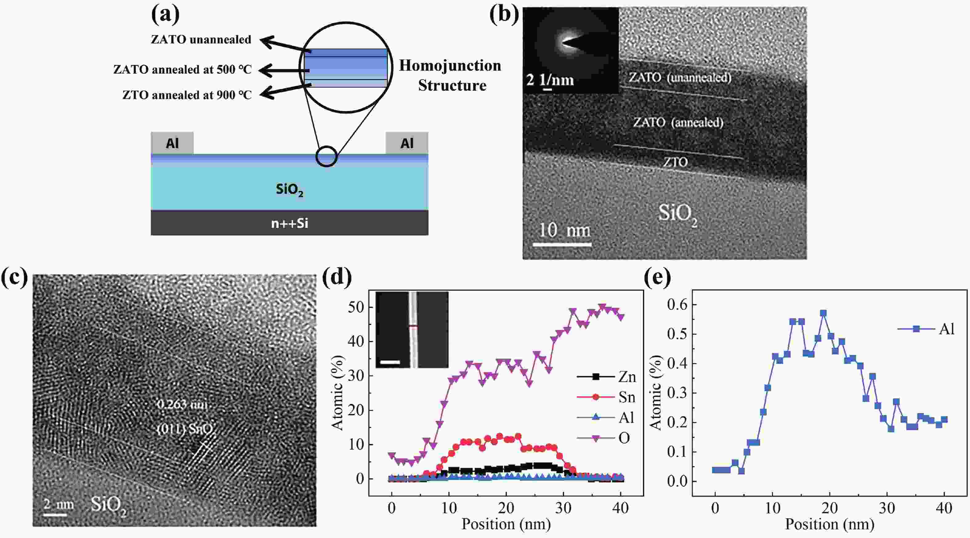
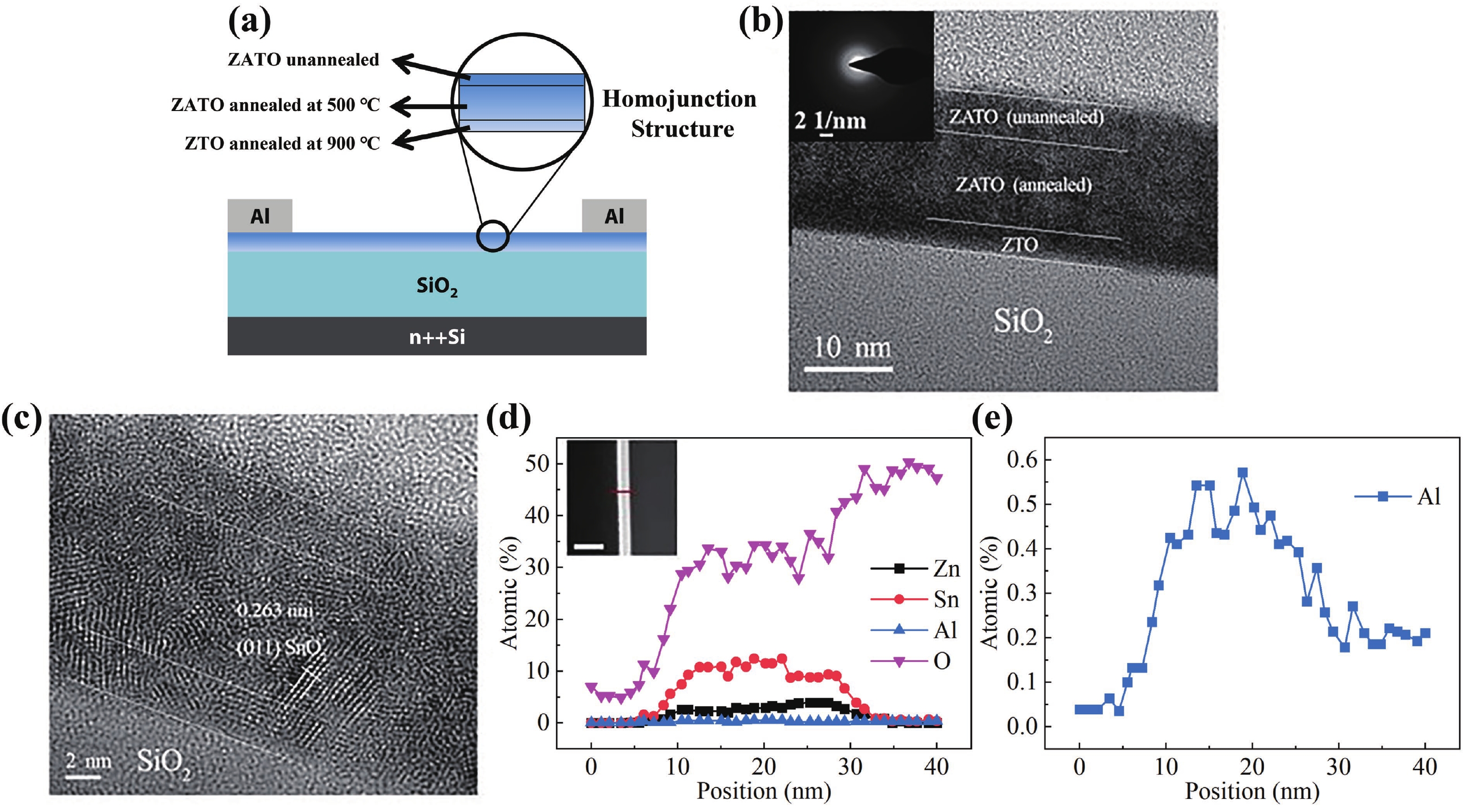
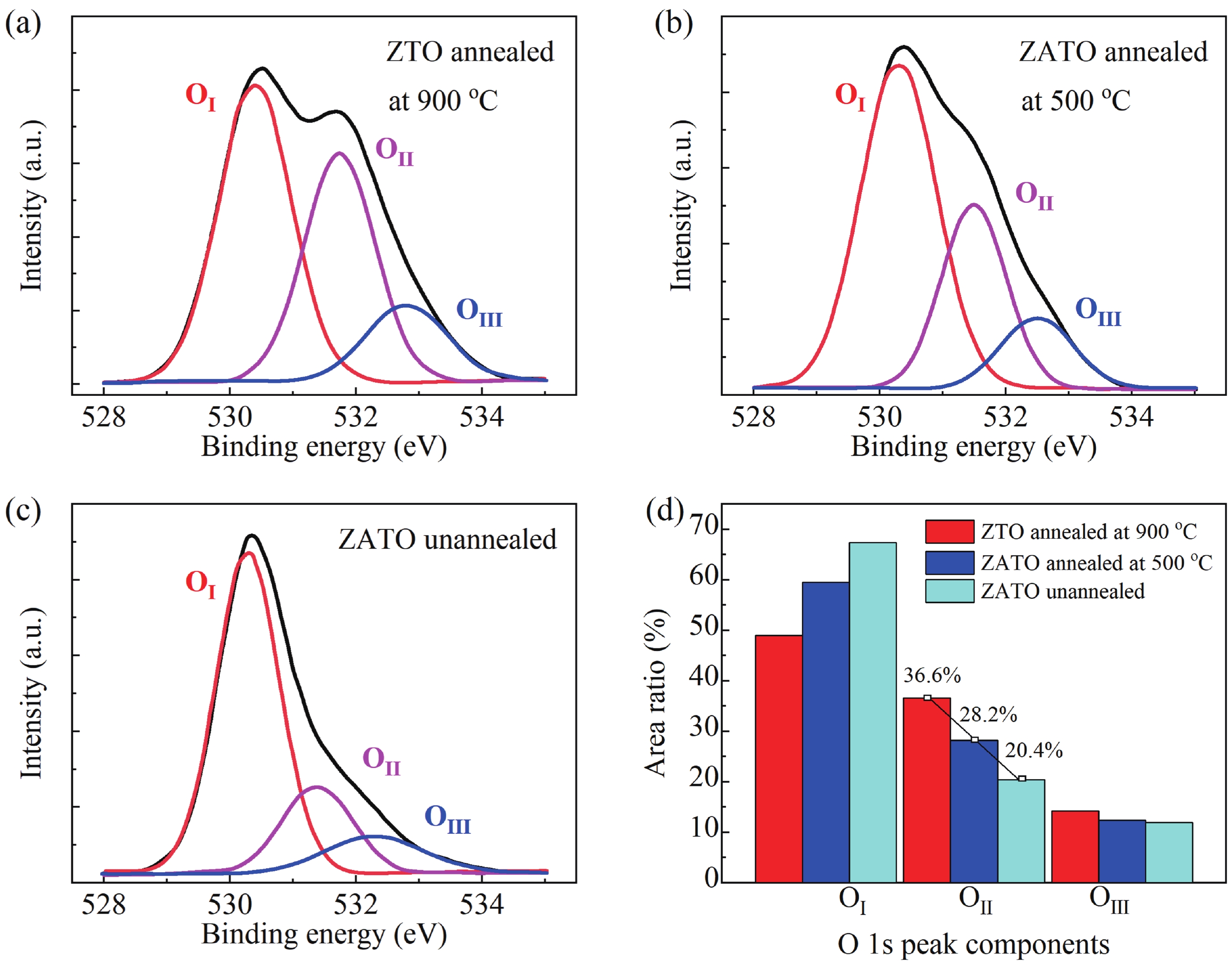
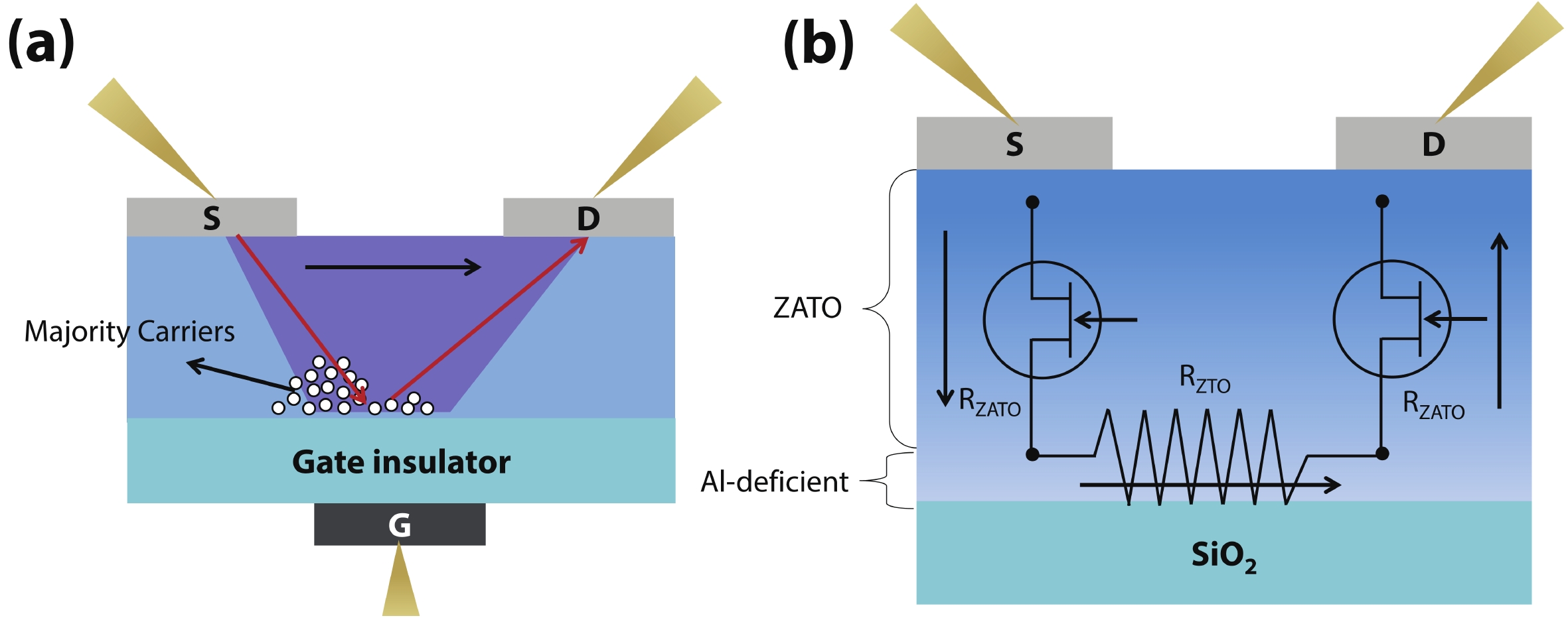
Amorphous oxide semiconductors (AOS) have unique advantages in transparent and flexible thin film transistors (TFTs) applications, compared to low-temperature polycrystalline-Si (LTPS). However, intrinsic AOS TFTs are difficult to obtain field-effect mobility (μFE) higher than LTPS (100 cm2/(V·s)). Here, we design ZnAlSnO (ZATO) homojunction structure TFTs to obtain μFE = 113.8 cm2/(V·s). The device demonstrates optimized comprehensive electrical properties with an off-current of about 1.5 × 10⁻¹¹ A, a threshold voltage of –1.71 V, and a subthreshold swing of 0.372 V/dec. There are two kinds of gradient coupled in the homojunction active layer, which are micro-crystallization and carrier suppressor concentration gradient distribution so that the device can reduce off-current and shift the threshold voltage positively while maintaining high field-effect mobility. Our research in the homojunction active layer points to a promising direction for obtaining excellent-performance AOS TFTs.

J. Semicond.
2023, 44(5): 052102 doi: 10.1088/1674-4926/44/5/052102
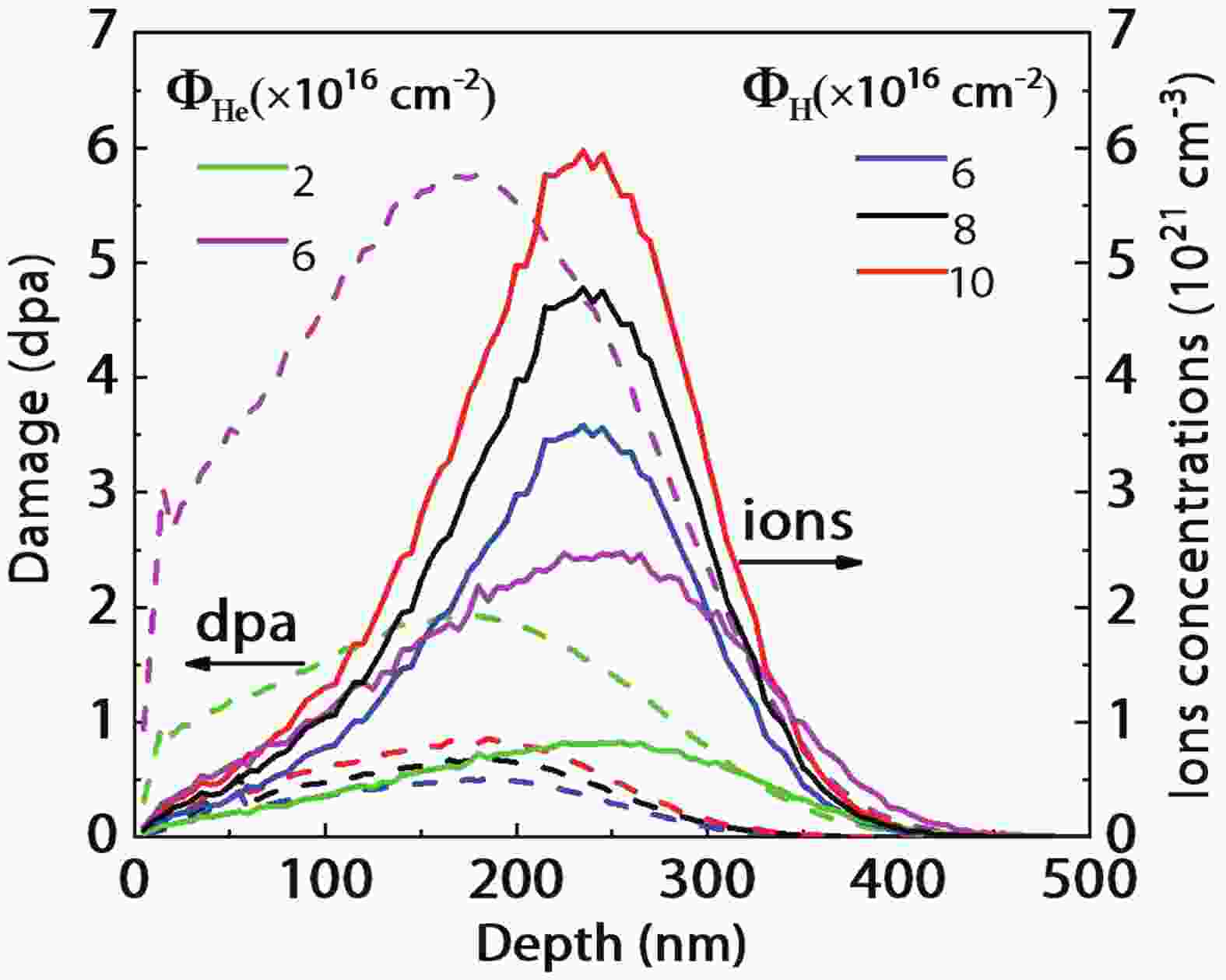
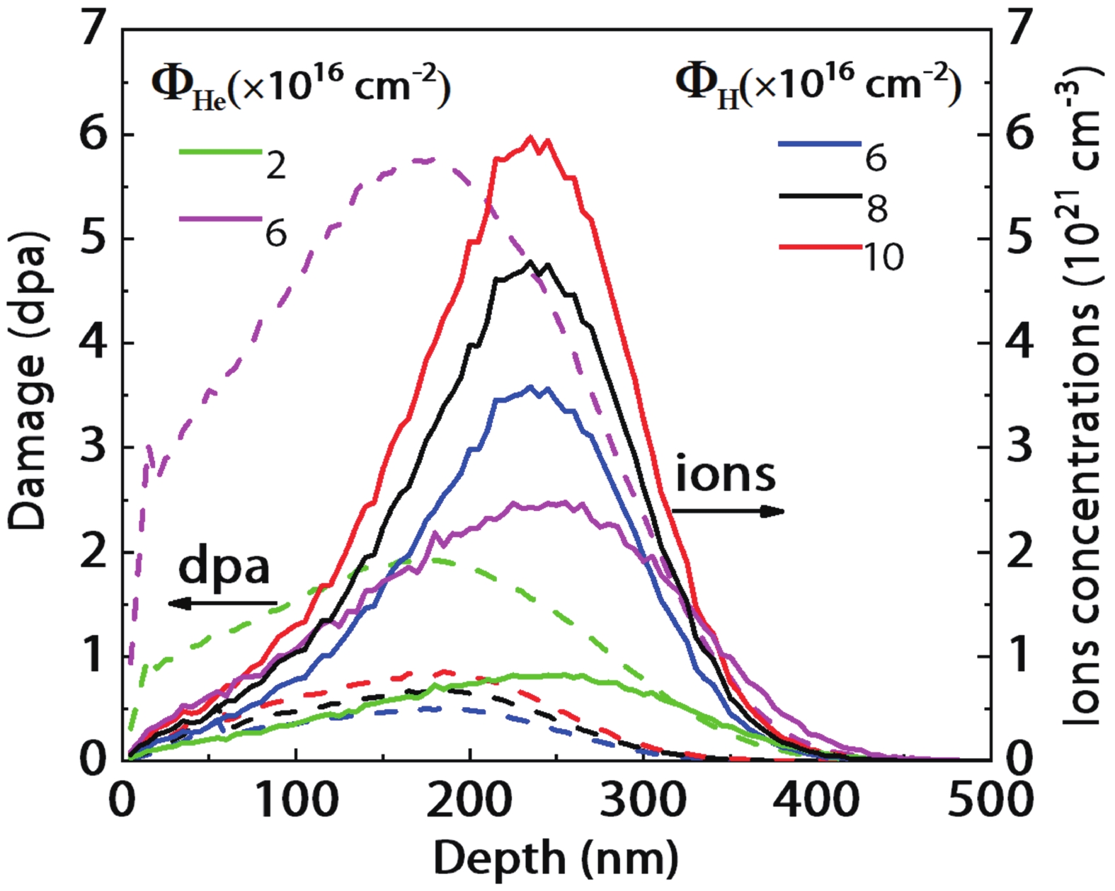
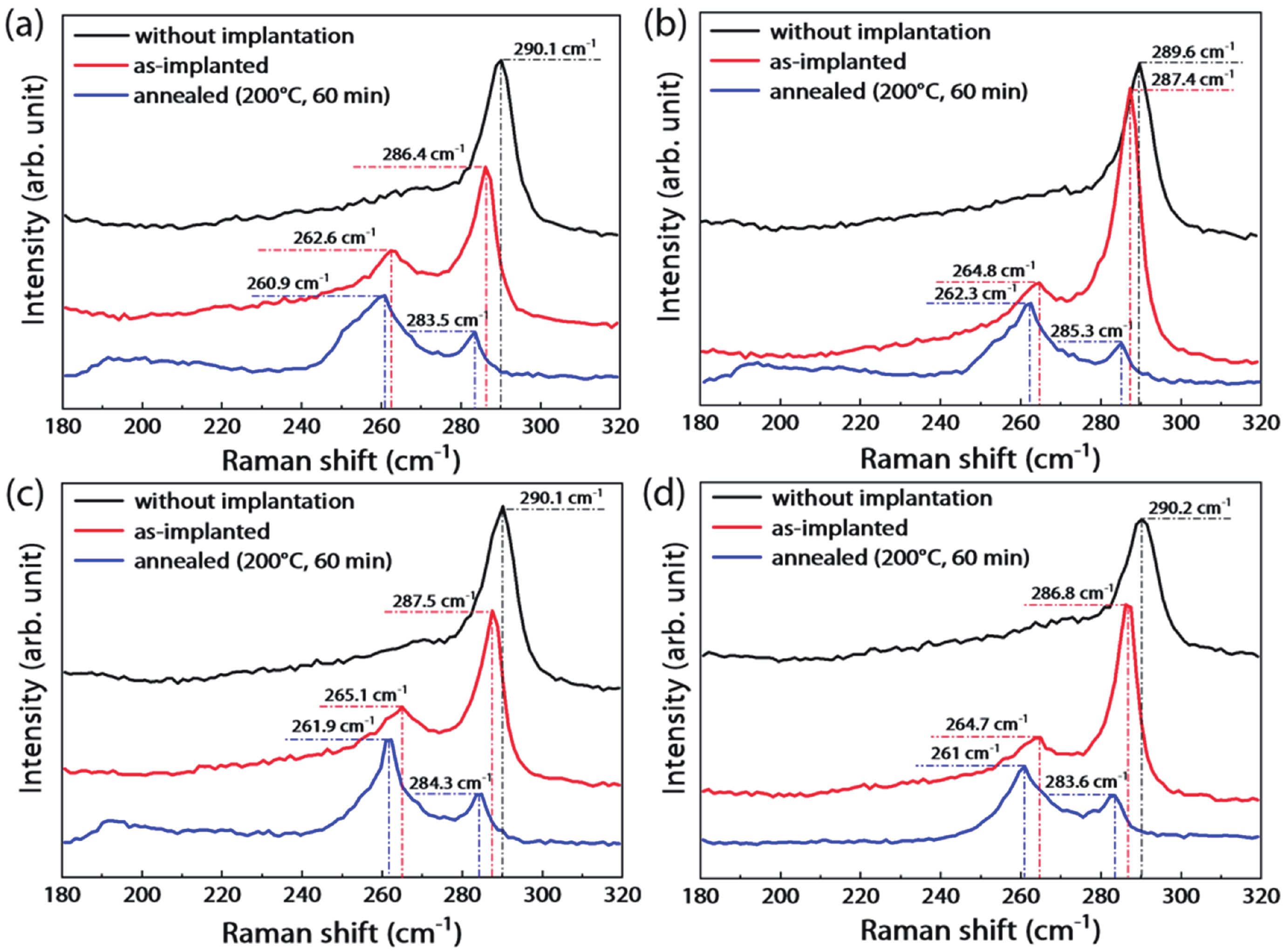
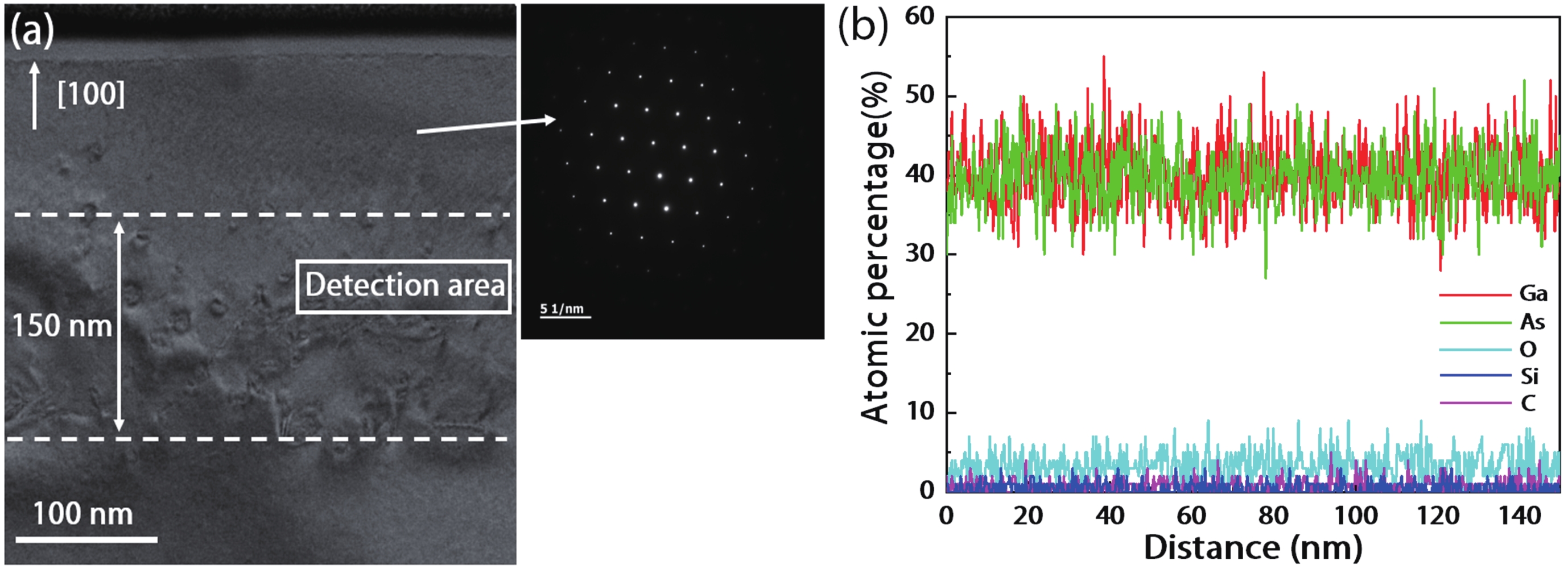
In this work, the surface morphology and internal defect evolution process of GaAs substrates implanted with light ions of different fluence combinations are studied. The influence of H and He ions implantation on the atomic mechanism of the blister phenomenon observed after annealing is investigated. Raman spectroscopy is used to measure the surface stress change of different samples before and after implantation and annealing. Optical microscopy and atomic force microscopy are used to characterize the morphology changes of the GaAs surface under different annealing conditions. The evolution of bubbles and defects in GaAs crystals is revealed by transmission electron microscopy. Through this study, it is hoped that ion implantation fluence, surface exfoliation efficiency and exfoliation cost can be optimized. At the same time, it also lays a foundation for the heterointegration of GaAs film on Si.


J. Semicond.
2023, 44(5): 052201 doi: 10.1088/1674-4926/44/5/052201
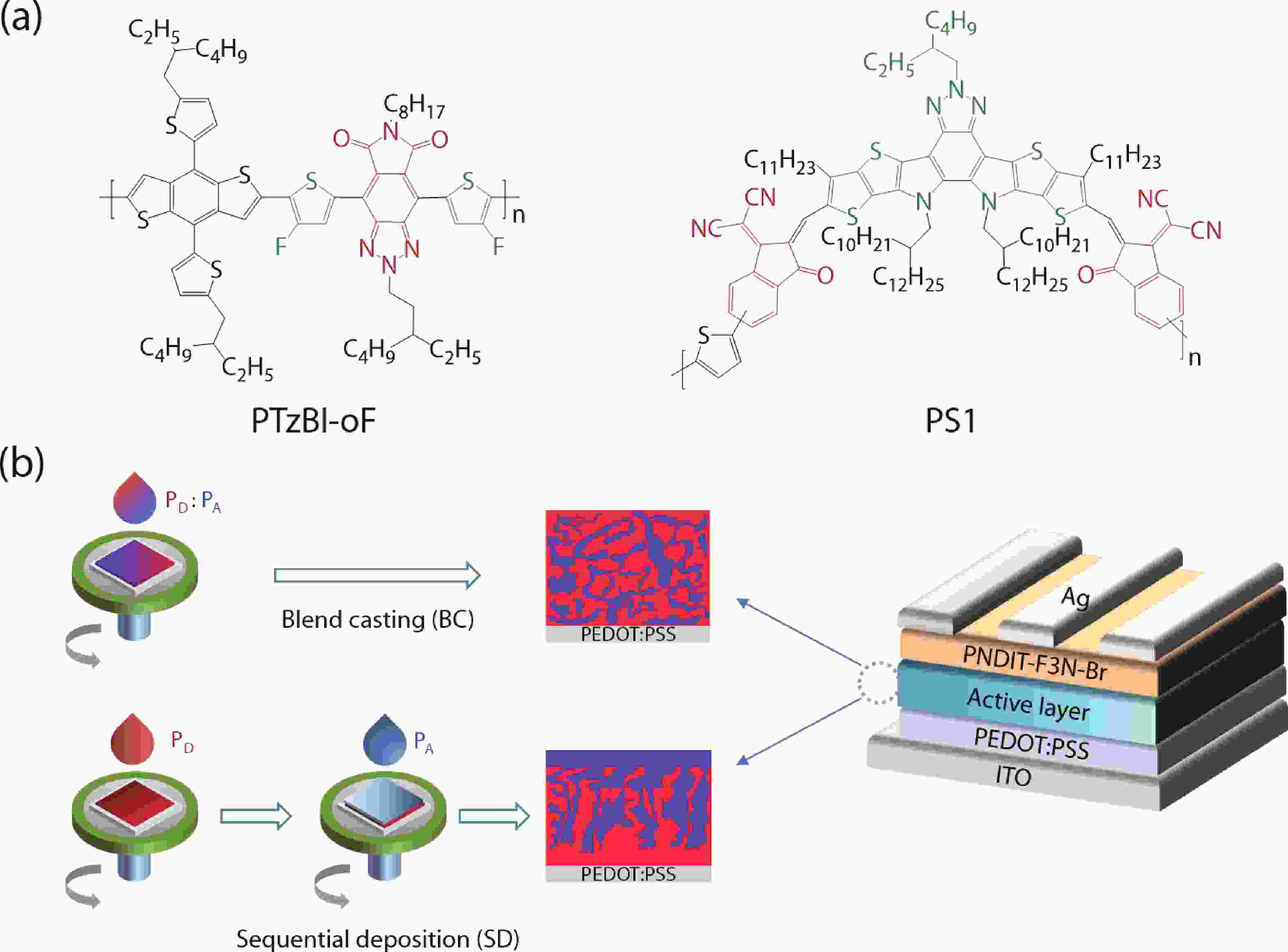
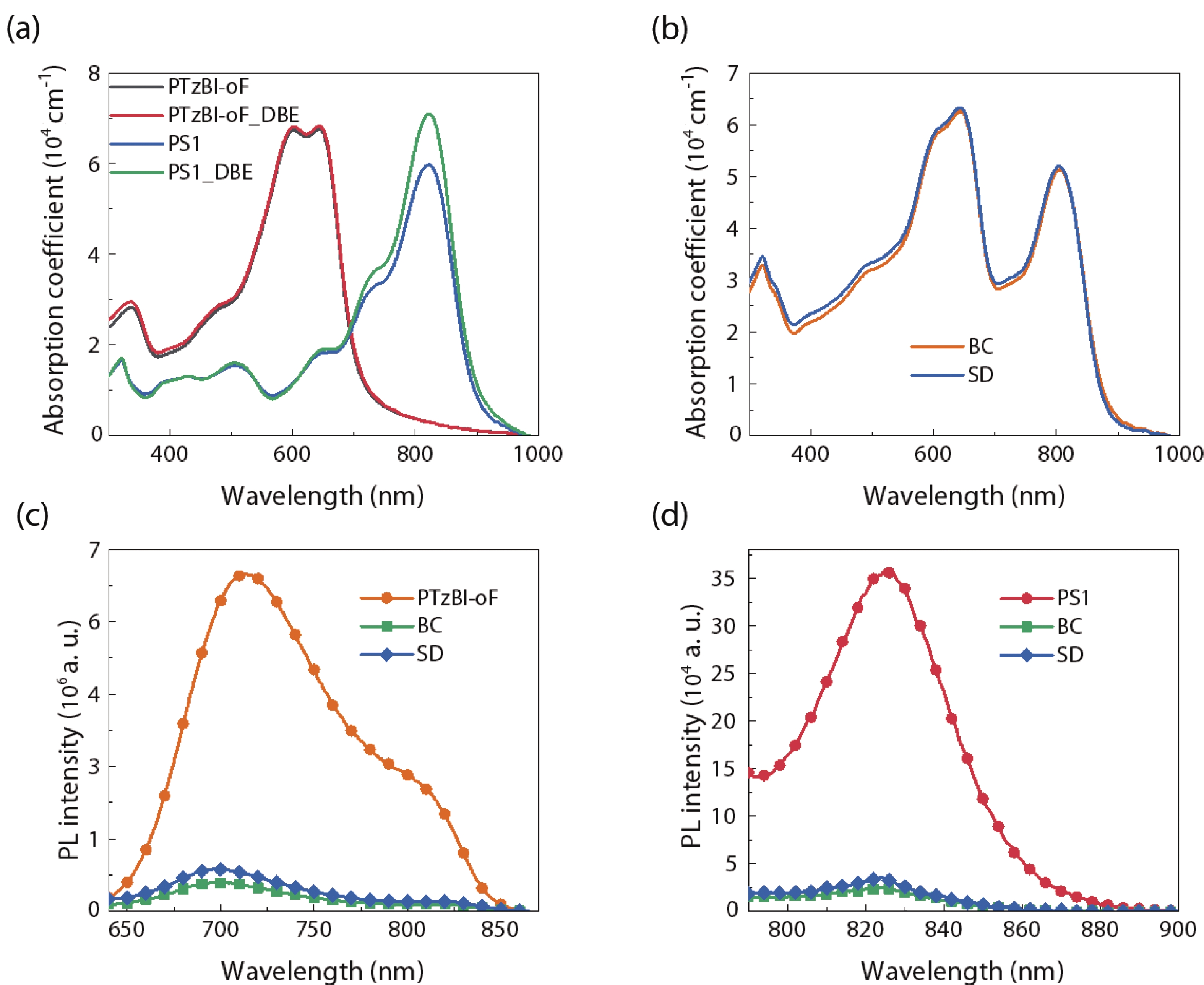
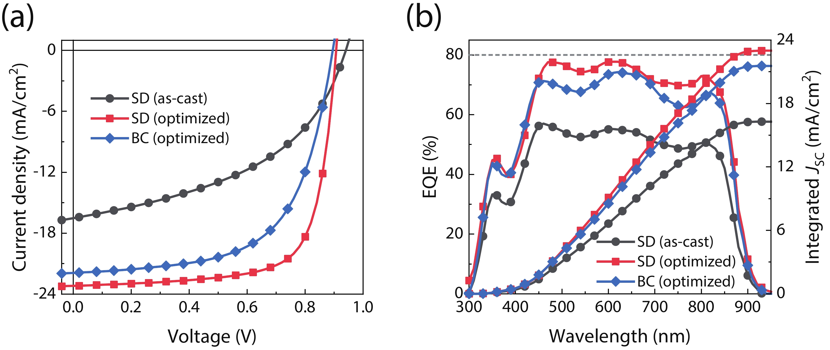
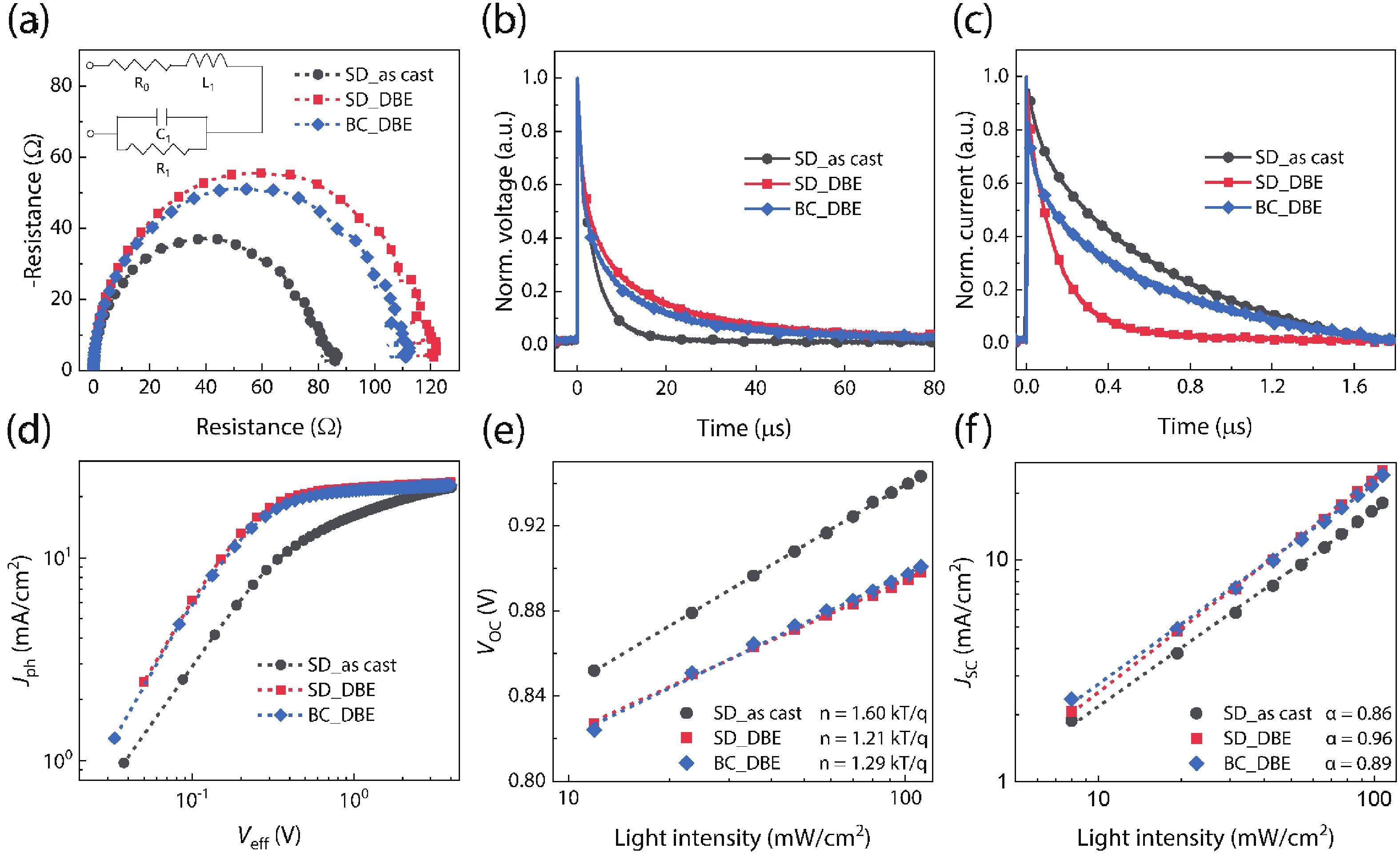
Due to the complicated film formation kinetics, morphology control remains a major challenge for the development of efficient and stable all-polymer solar cells (all-PSCs). To overcome this obstacle, the sequential deposition method is used to fabricate the photoactive layers of all-PSCs comprising a polymer donor PTzBI-oF and a polymer acceptor PS1. The film morphology can be manipulated by incorporating amounts of a dibenzyl ether additive into the PS1 layer. Detailed morphology investigations by grazing incidence wide-angle X-ray scattering and a transmission electron microscope reveal that the combination merits of sequential deposition and DBE additive can render favorable crystalline properties as well as phase separation for PTzBI-oF:PS1 blends. Consequently, the optimized all-PSCs delivered an enhanced power conversion efficiency (PCE) of 15.21% along with improved carrier extraction and suppressed charge recombination. More importantly, the optimized all-PSCs remain over 90% of their initial PCEs under continuous thermal stress at 65 °C for over 500 h. This work validates that control over microstructure morphology via a sequential deposition process is a promising strategy for fabricating highly efficient and stable all-PSCs.


J. Semicond.
2023, 44(5): 052701 doi: 10.1088/1674-4926/44/5/052701
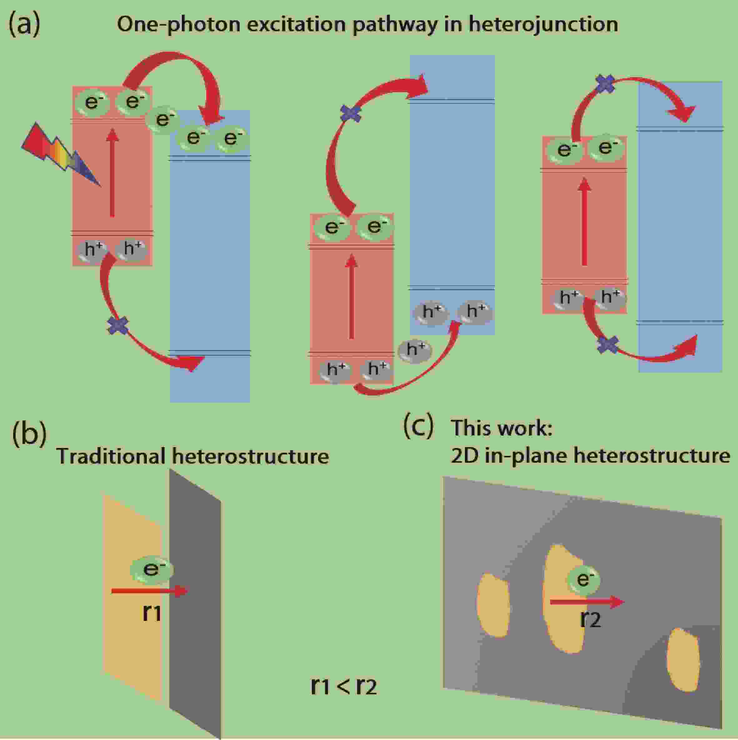
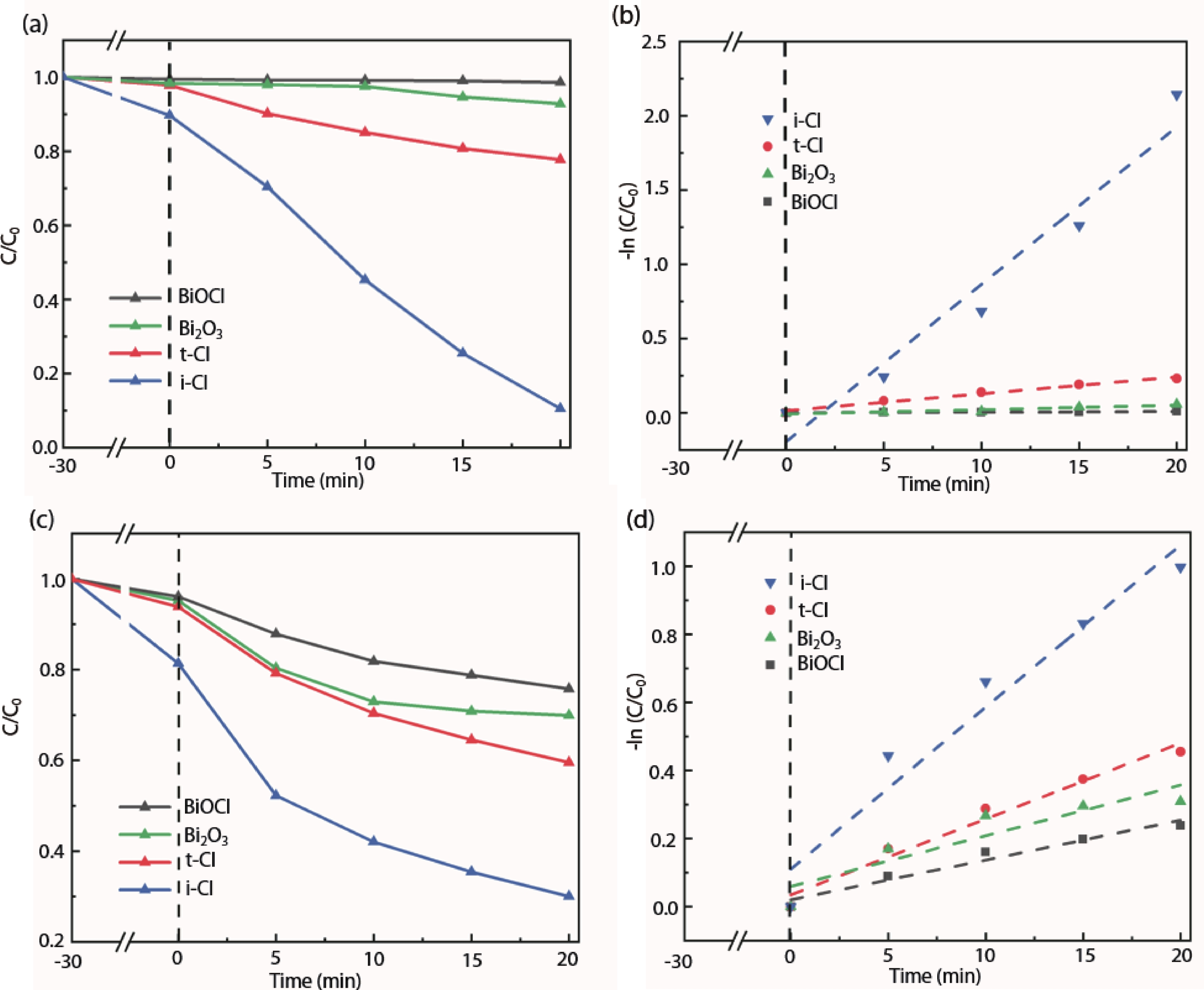
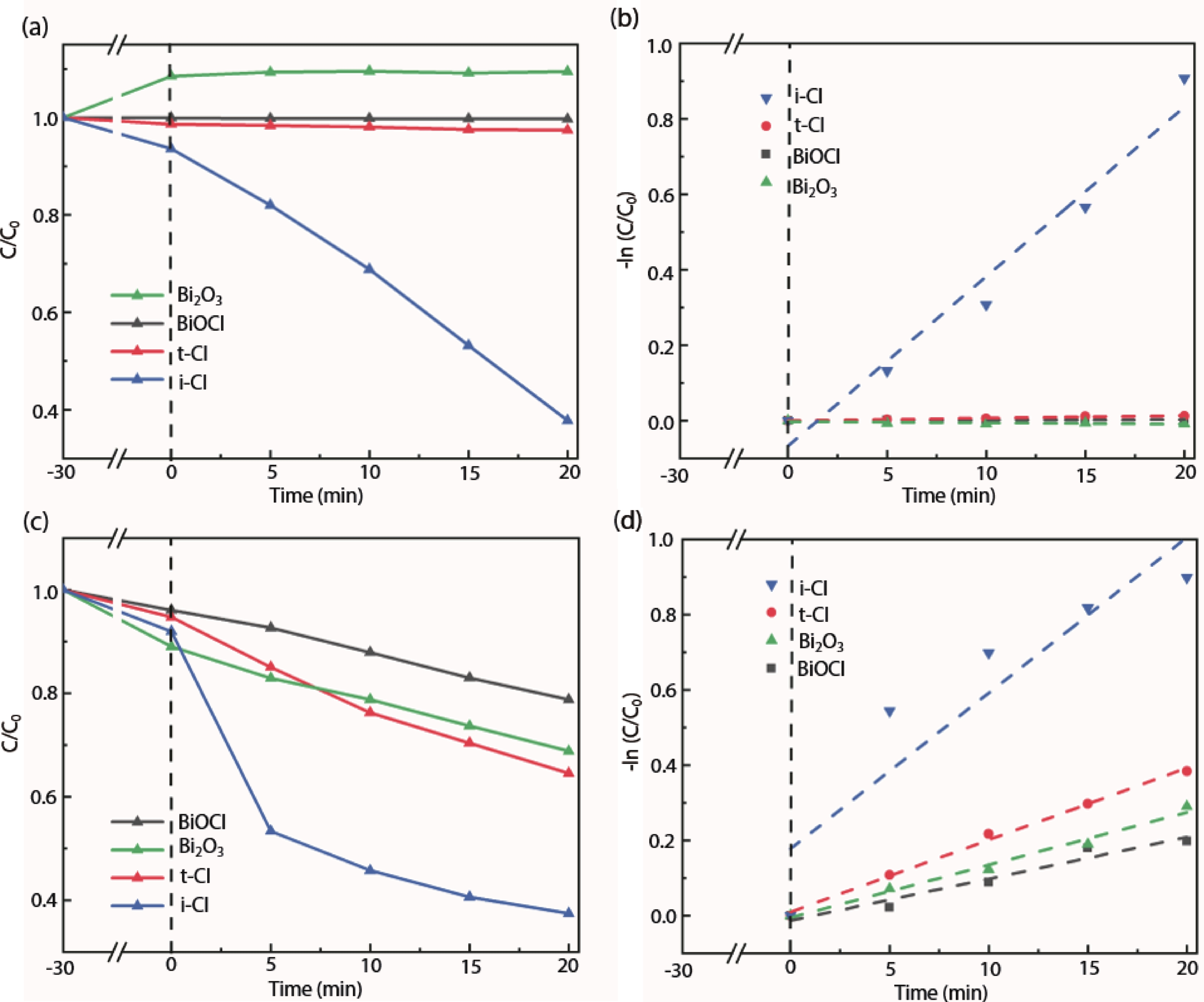
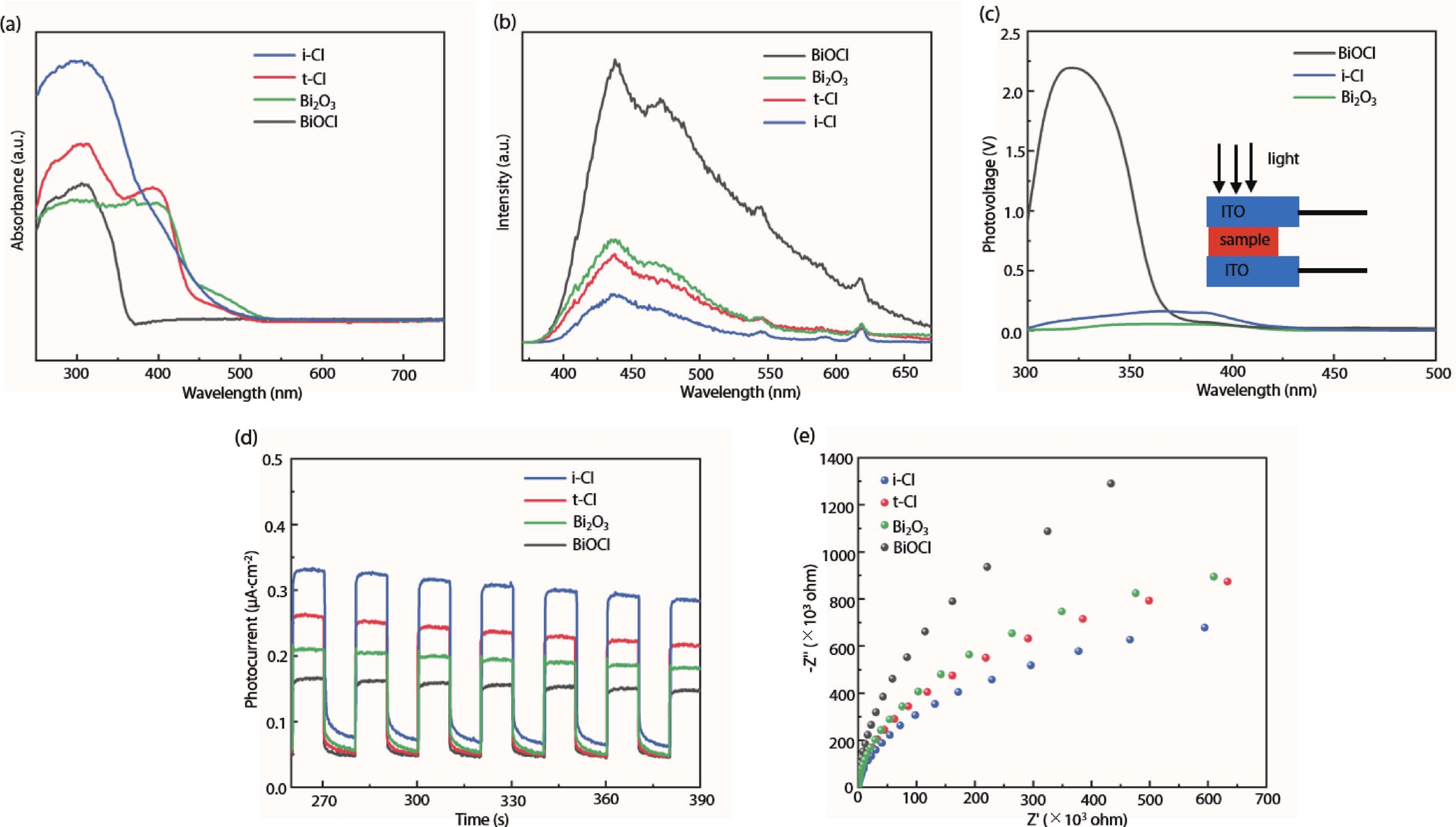
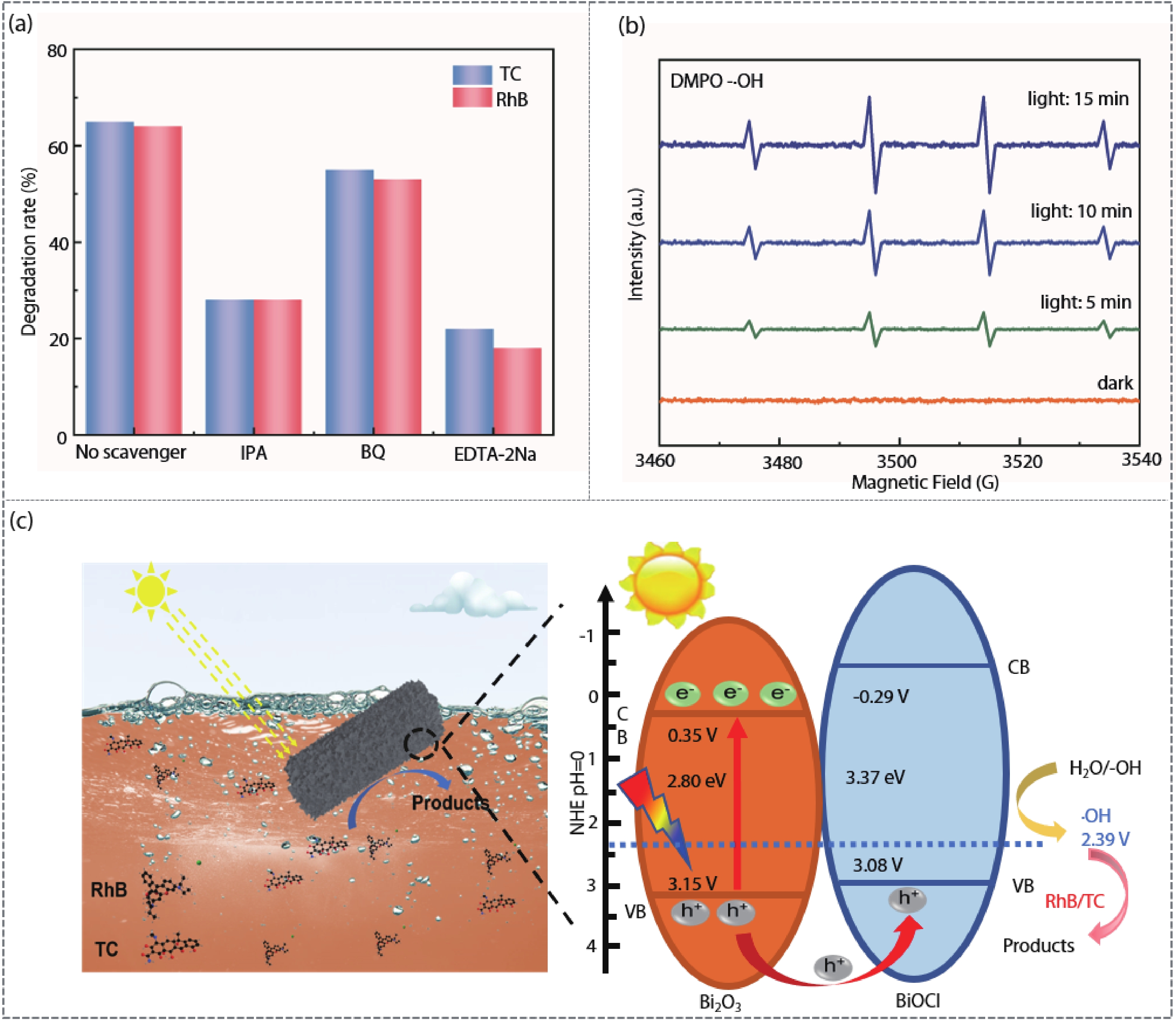
Broad-spectrum absorption and highly effective charge-carrier separation are two essential requirements to improve the photocatalytic performance of semiconductor-based photocatalysts. In this work, a fascinating one-photon system is reported by rationally fabricating 2D in-plane Bi2O3/BiOCl (i-Cl) heterostructures for efficient photocatalytic degradation of RhB and TC. Systematic investigations revealed that the matched band structure generated an internal electric field and a chemical bond connection between the Bi2O3 and BiOCl in the Bi2O3/BiOCl composite that could effectively improve the utilization ratio of visible light and the separation effectivity of photo-generated carriers in space. The formed interactions at the 2D in-plane heterojunction interface induced the one-photon excitation pathway which has been confirmed by the experiment and DFT calculations. As a result, the i-Cl samples showed significantly enhanced photocatalytic efficiency towards the degradation of RhB and TC (RhB: 0.106 min−1; TC: 0.048 min−1) under visible light. The degradation activities of RhB and TC for i-Cl were 265.08 and 4.08 times that of pure BiOCl, as well as 9.27 and 2.14 times that of mechanistically mixed Bi2O3/BiOCl samples, respectively. This work provides a logical strategy to construct other 2D in-plane heterojunctions with a one-photon excitation pathway with enhanced performance.


J. Semicond.
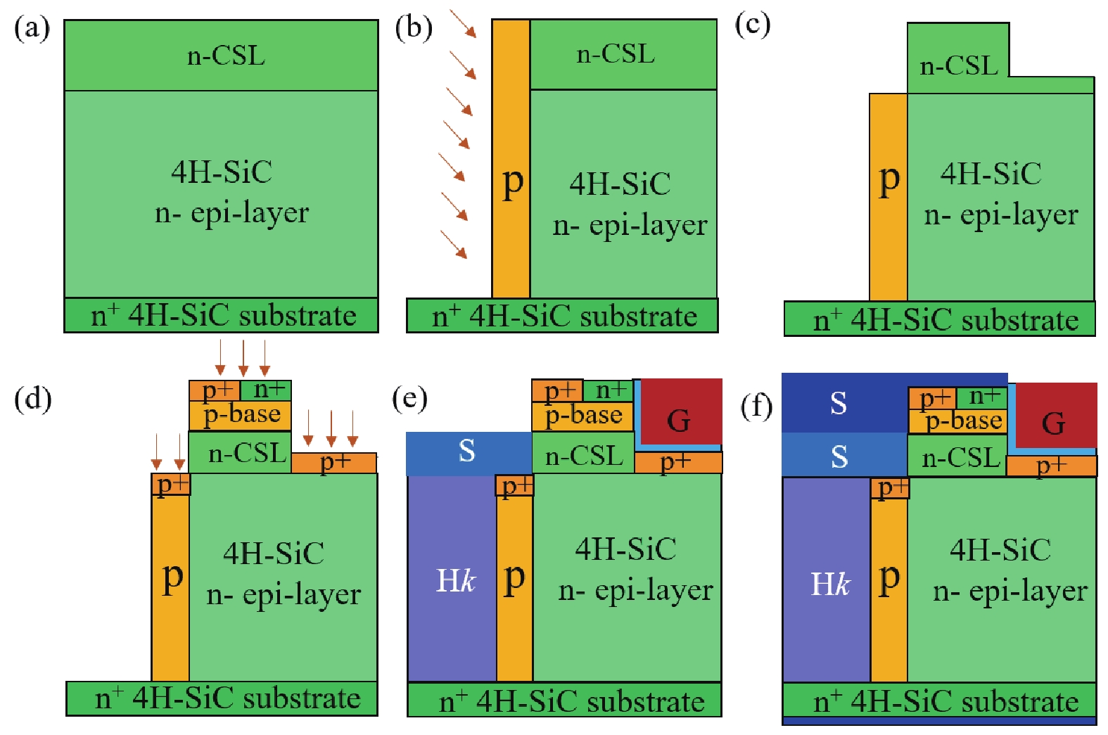
2023, 44(5): 052801 doi: 10.1088/1674-4926/44/5/052801

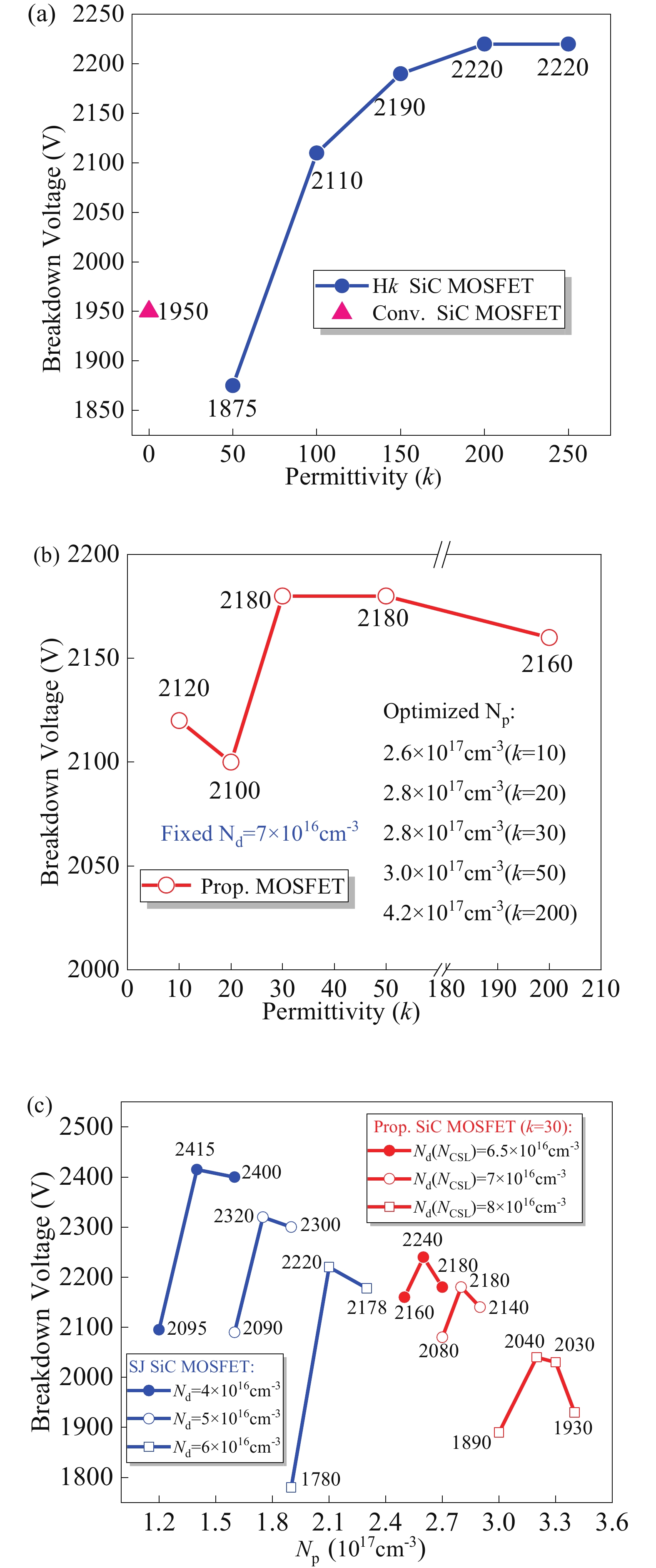
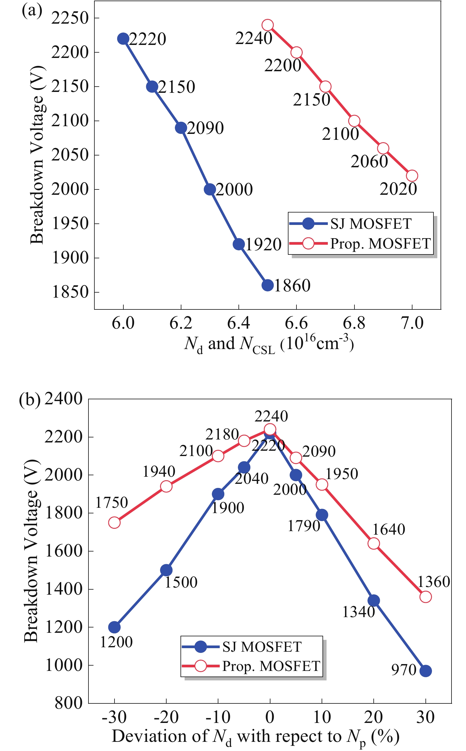
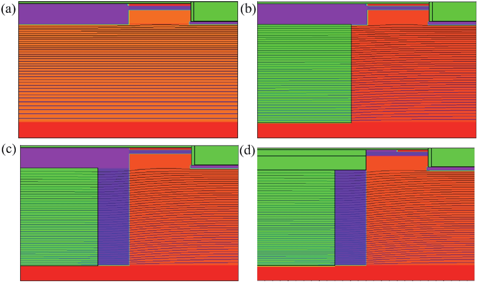
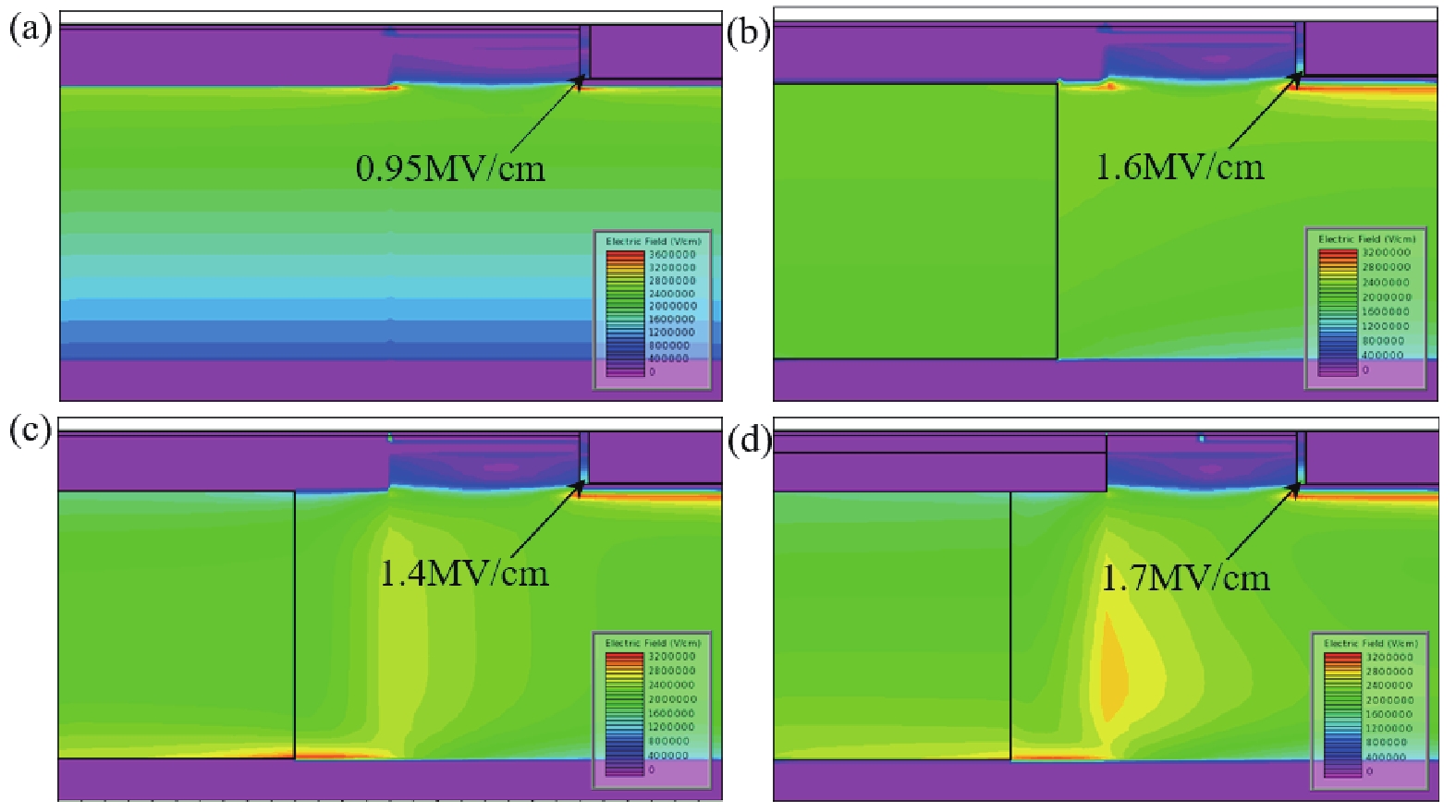
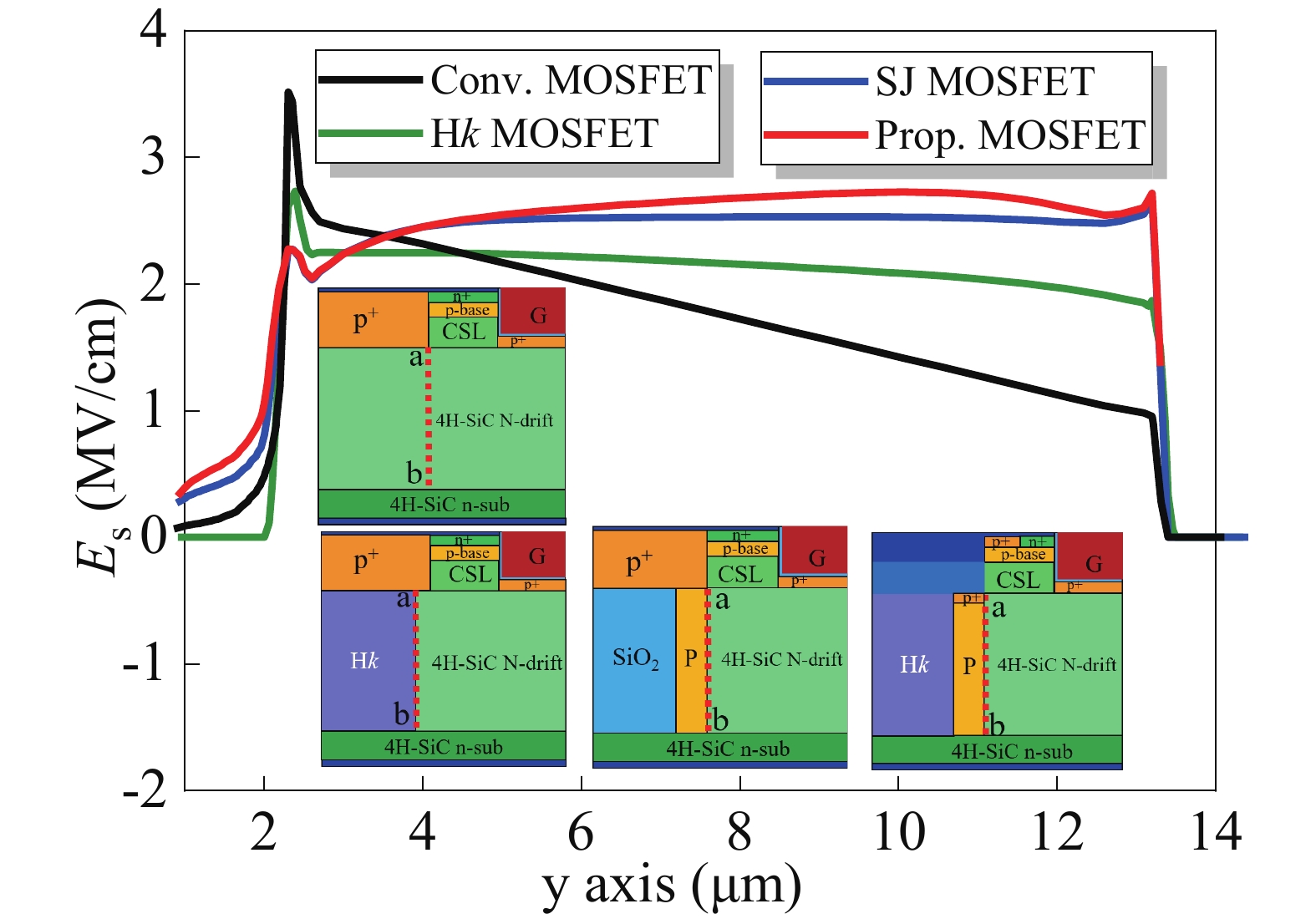
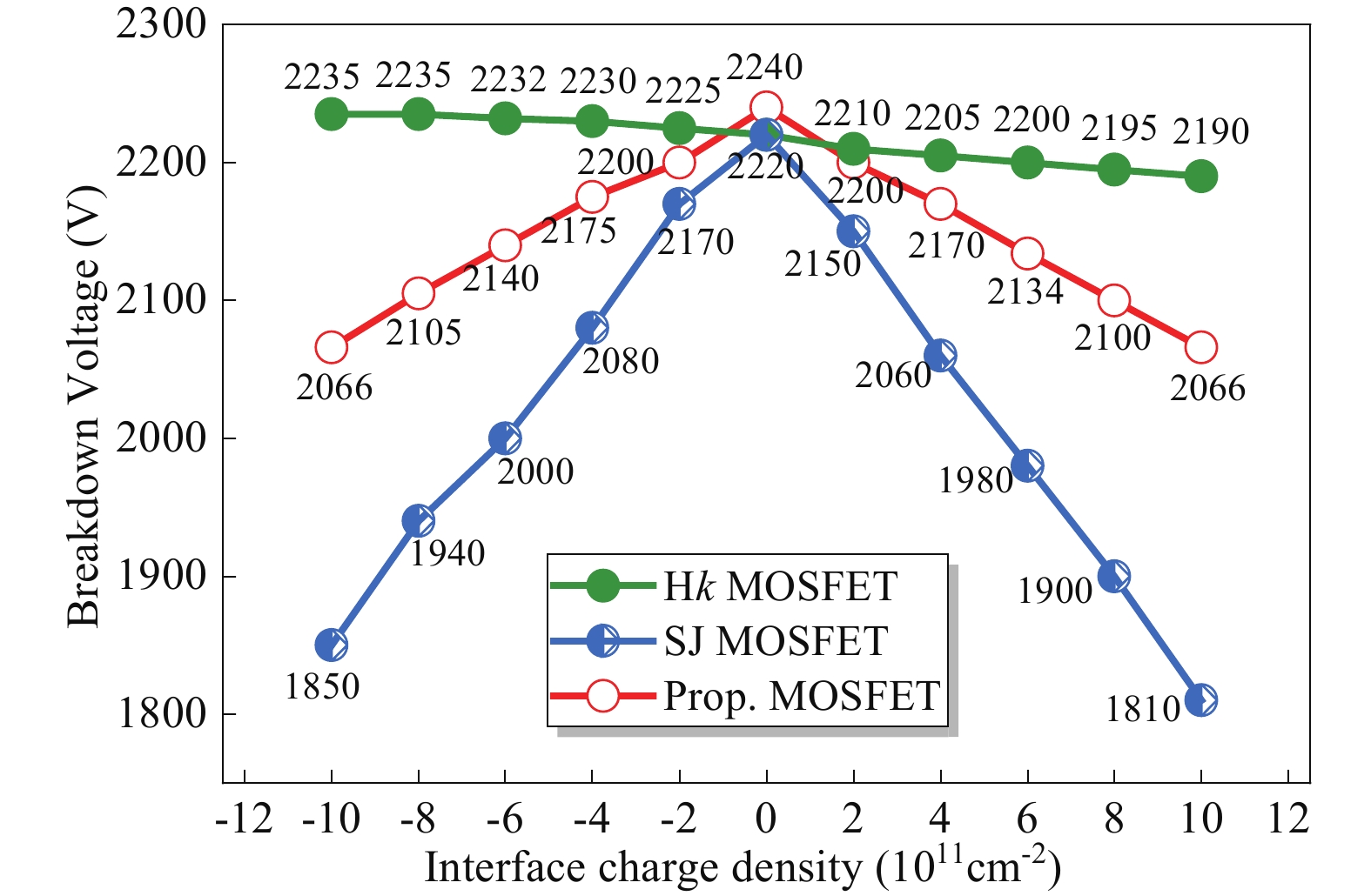
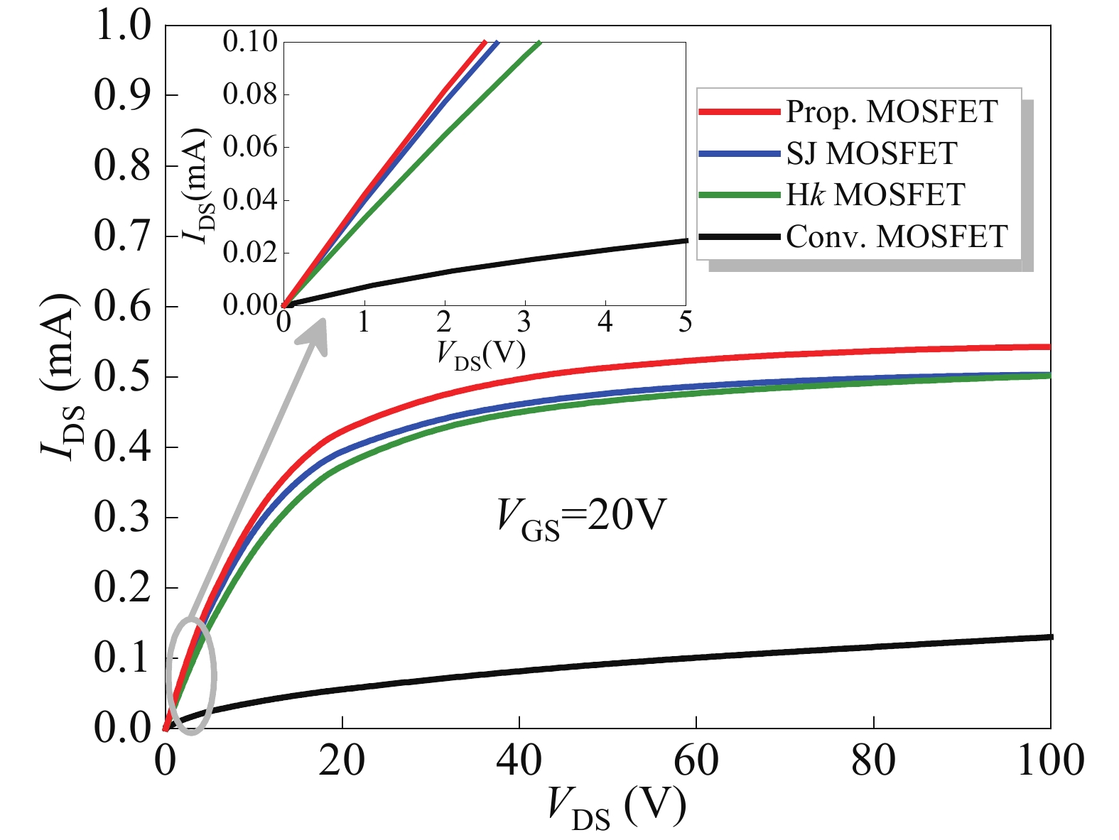
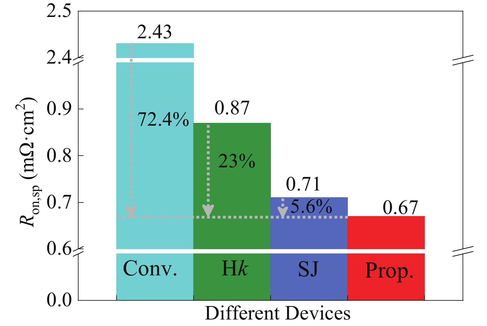
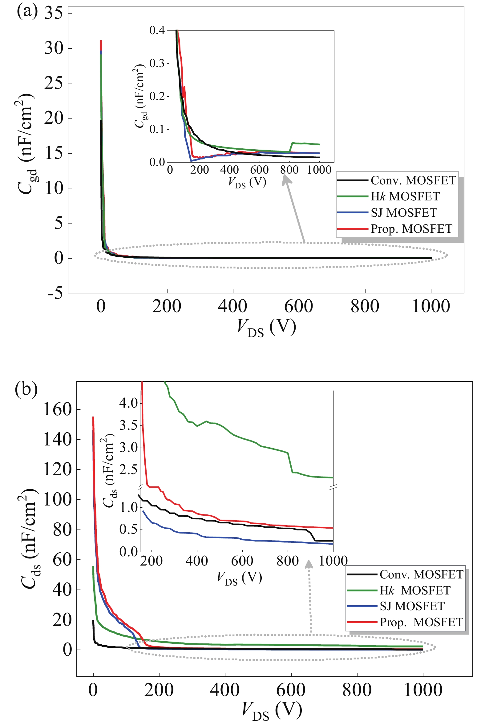
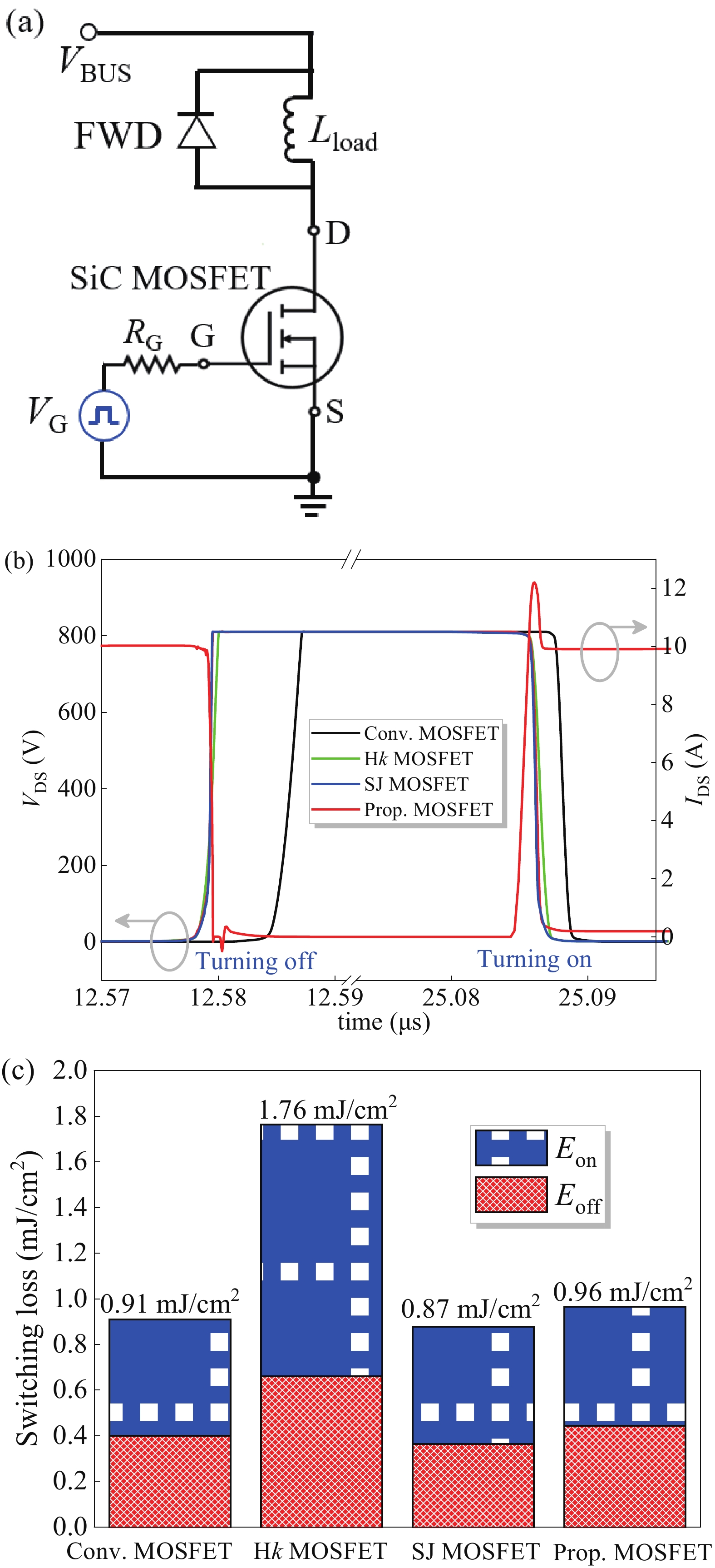
A new SiC superjunction power MOSFET device using high-k insulator and p-type pillar with an integrated Schottky barrier diode (Hk-SJ-SBD MOSFET) is proposed, and has been compared with the SiC high-k MOSFET (Hk MOSFET), SiC superjuction MOSFET (SJ MOSFET) and the conventional SiC MOSFET in this article. In the proposed SiC Hk-SJ-SBD MOSFET, under the combined action of the p-type region and the Hk dielectric layer in the drift region, the concentration of the N-drift region and the current spreading layer can be increased to achieve an ultra-low specific on-resistance (Ron,sp). The integrated Schottky barrier diode (SBD) also greatly improves the reverse recovery performance of the device. TCAD simulation results indicate that the Ron,sp of the proposed SiC Hk-SJ-SBD MOSFET is 0.67 mΩ·cm2 with a 2240 V breakdown voltage (BV), which is more than 72.4%, 23%, 5.6% lower than that of the conventional SiC MOSFET, Hk SiC MOSFET and SJ SiC MOSFET with the 1950, 2220, and 2220 V BV, respectively. The reverse recovery time and reverse recovery charge of the proposed MOSFET is 16 ns and18 nC, which are greatly reduced by more than 74% and 94% in comparison with those of all the conventional SiC MOSFET, Hk SiC MOSFET and SJ SiC MOSFET, due to the integrated SBD in the proposed MOSFET. And the trade-off relationship between the Ron,sp and the BV is also significantly improved compared with that of the conventional MOSFET, Hk MOSFET and SJ MOSFET as well as the MOSFETs in other previous literature, respectively. In addition, compared with conventional SJ SiC MOSFET, the proposed SiC MOSFET has better immunity to charge imbalance, which may bring great application prospects.


J. Semicond.
2023, 44(5): 052802 doi: 10.1088/1674-4926/44/5/052802

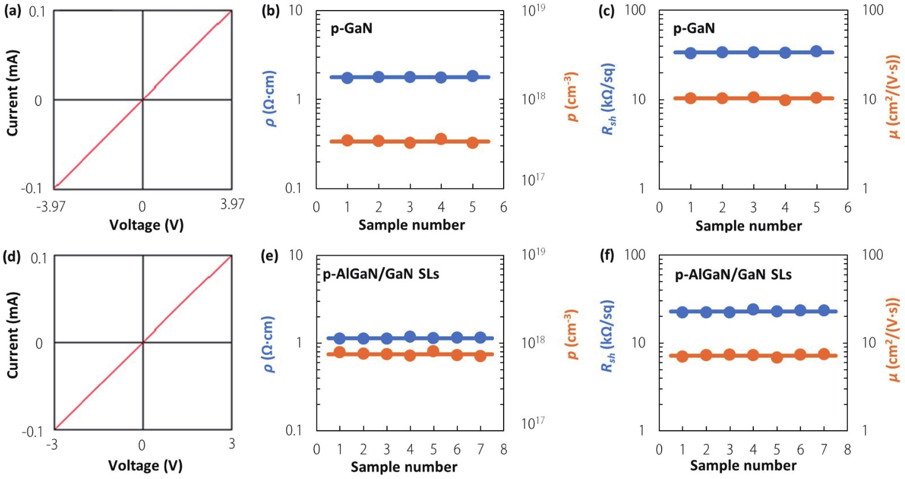
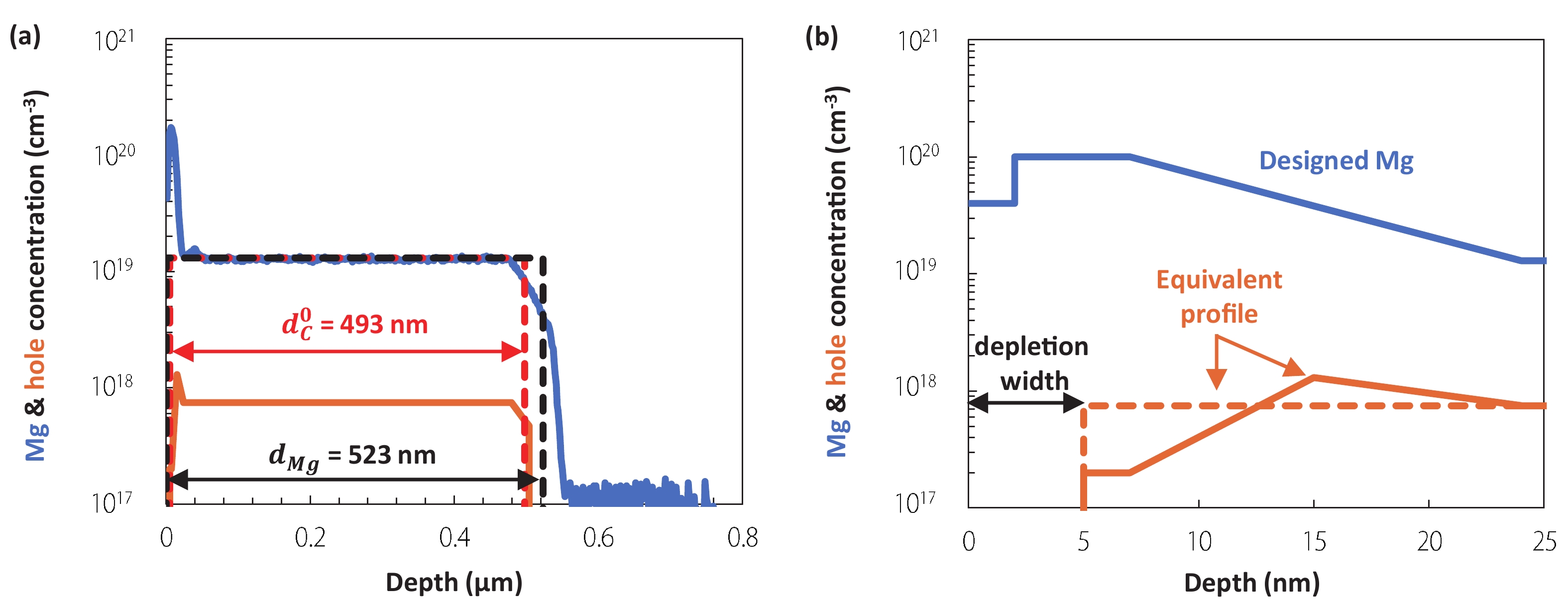
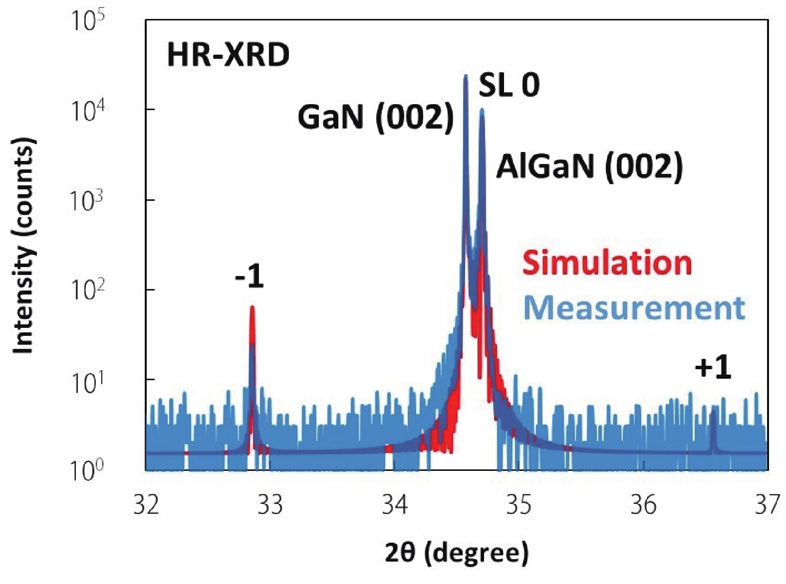
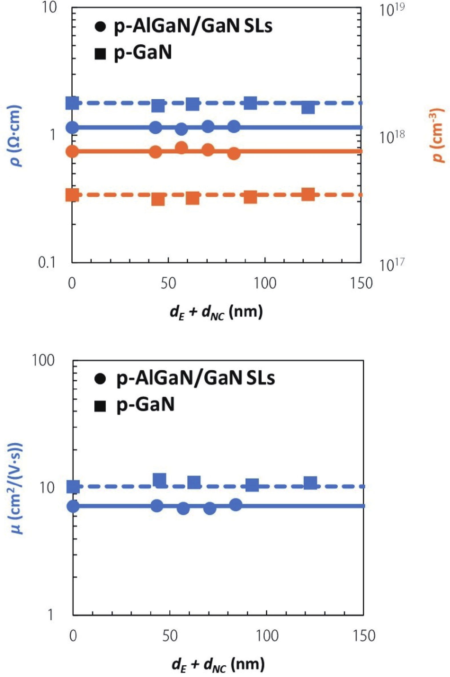
A suitable contacting scheme for p-(Al)GaN facilitating quick feedback and accurate measurements is proposed in this study. 22 nm p+-GaN followed by 2 nm p-In0.2Ga0.8N was grown on p-type layers by metal-organic chemical vapor deposition. Samples were then cut into squares after annealing and contact electrodes using In balls were put at the corners of the squares. Good linearity between all the electrodes was confirmed in I–V curves during Hall measurements even with In metal. Serval samples taken from the same wafer showed small standard deviation of ~ 4% for resistivity, Hall mobility and hole concentration. The influence of contact layer on the electrical characteristics of bulk p-type layers was then investigated by step etching technique using inductively coupled plasma etching and subsequent Hall-effect measurements. Identical values could be obtained consistently when a 28 nm non-conductive layer thickness at the surface was taken into account. Therefore, the procedures for evaluating the electrical properties of GaN-based p-type layers just using In balls proposed in this study are shown to be quick and useful as for the other conventional III–V materials.


J. Semicond.
2023, 44(5): 052901 doi: 10.1088/1674-4926/44/5/052901

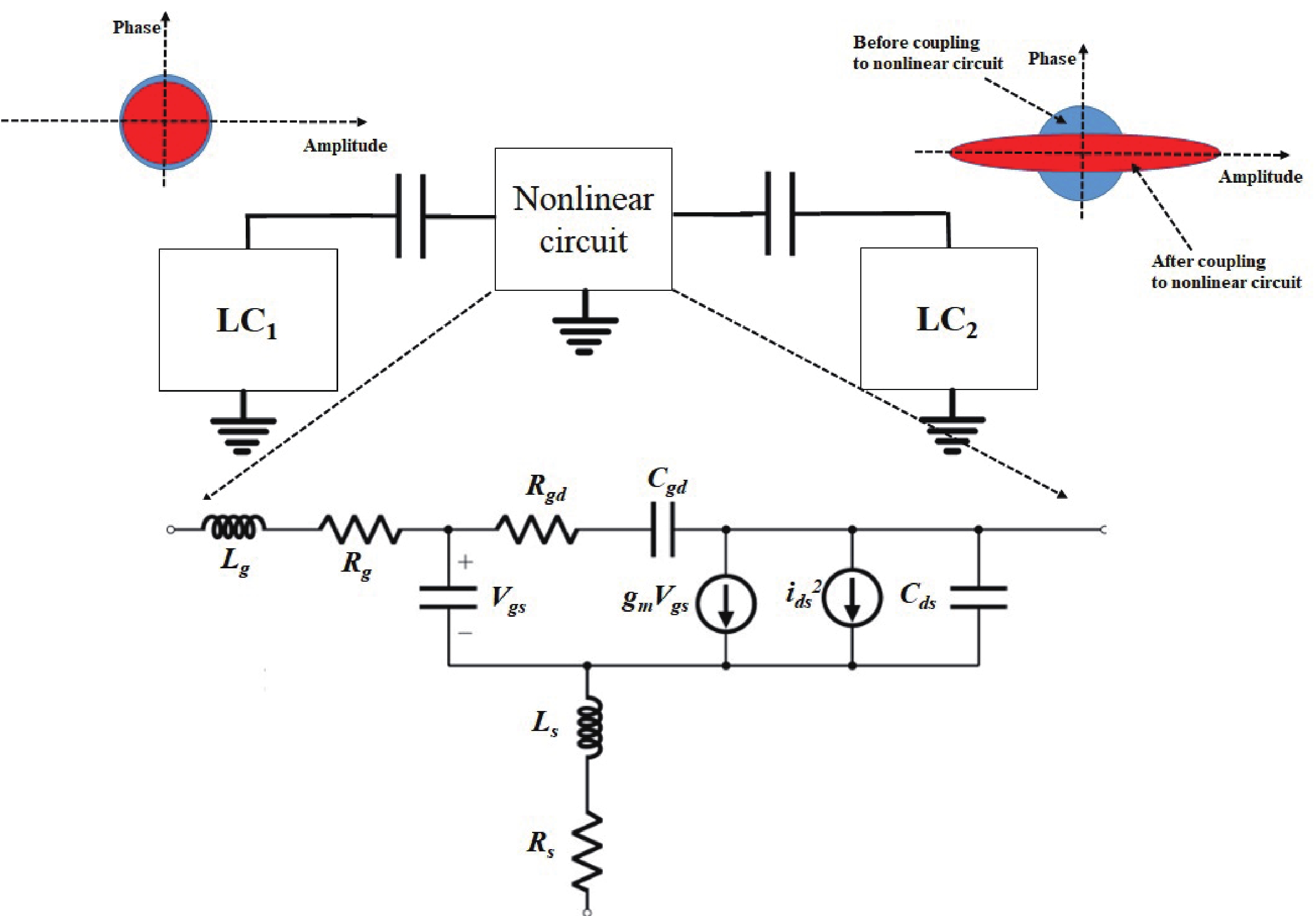
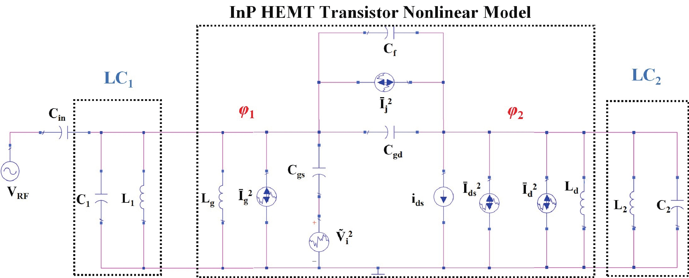
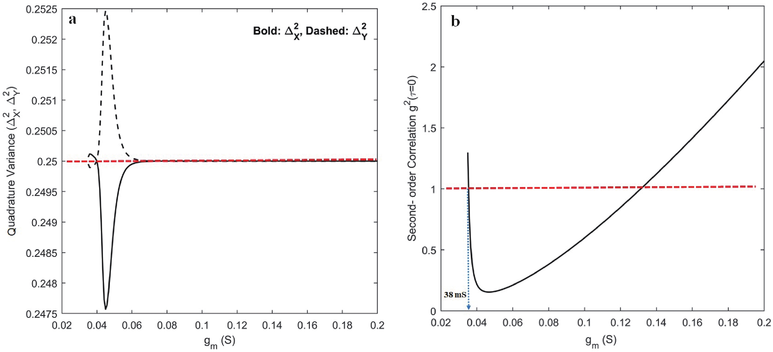
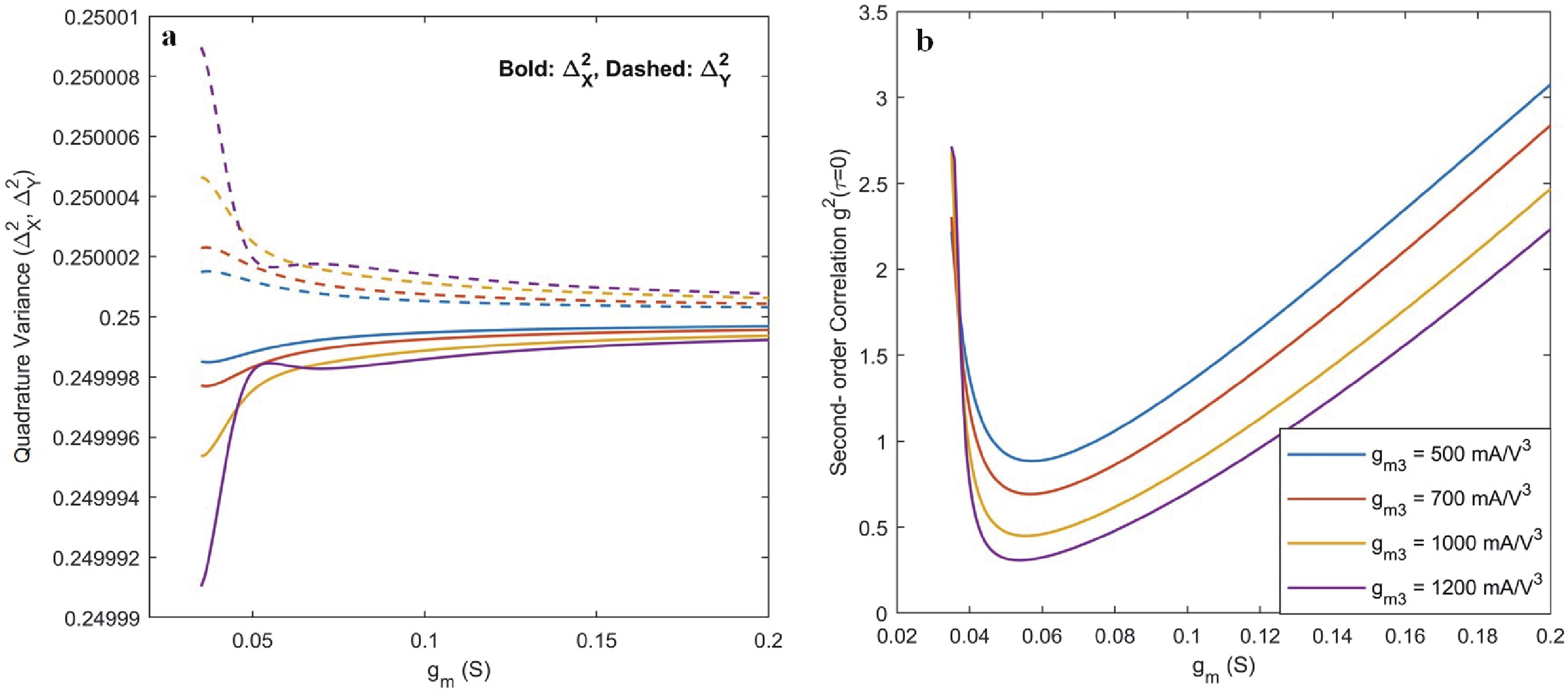
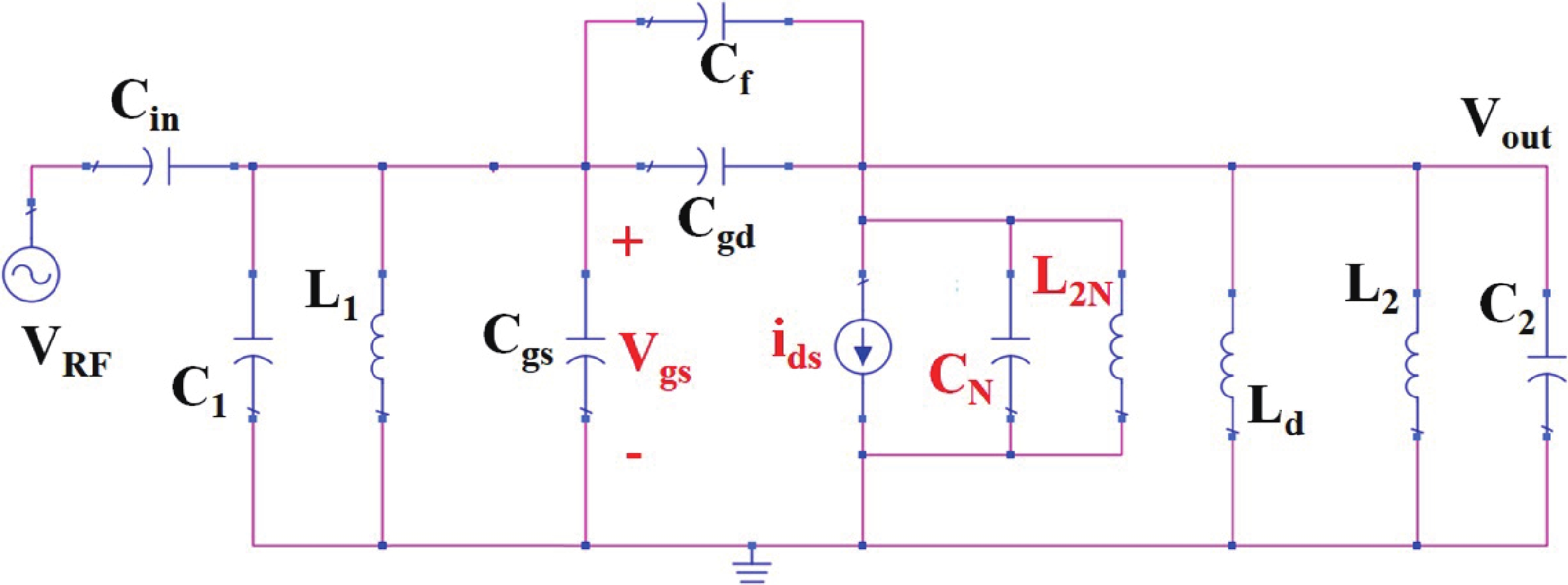
This study focuses on generating and manipulating squeezed states with two external oscillators coupled by an InP HEMT operating at cryogenic temperatures. First, the small-signal nonlinear model of the transistor at high frequency at 5 K is analyzed using quantum theory, and the related Lagrangian is theoretically derived. Subsequently, the total quantum Hamiltonian of the system is derived using Legendre transformation. The Hamiltonian of the system includes linear and nonlinear terms by which the effects on the time evolution of the states are studied. The main result shows that the squeezed state can be generated owing to the transistor’s nonlinearity; more importantly, it can be manipulated by some specific terms introduced in the nonlinear Hamiltonian. In fact, the nonlinearity of the transistors induces some effects, such as capacitance, inductance, and second-order transconductance, by which the properties of the external oscillators are changed. These changes may lead to squeezing or manipulating the parameters related to squeezing in the oscillators. In addition, it is theoretically derived that the circuit can generate two-mode squeezing. Finally, second-order correlation (photon counting statistics) is studied, and the results demonstrate that the designed circuit exhibits antibunching, where the quadrature operator shows squeezing behavior.

J. Semicond.
2023, 44(5): 054101 doi: 10.1088/1674-4926/44/5/054101
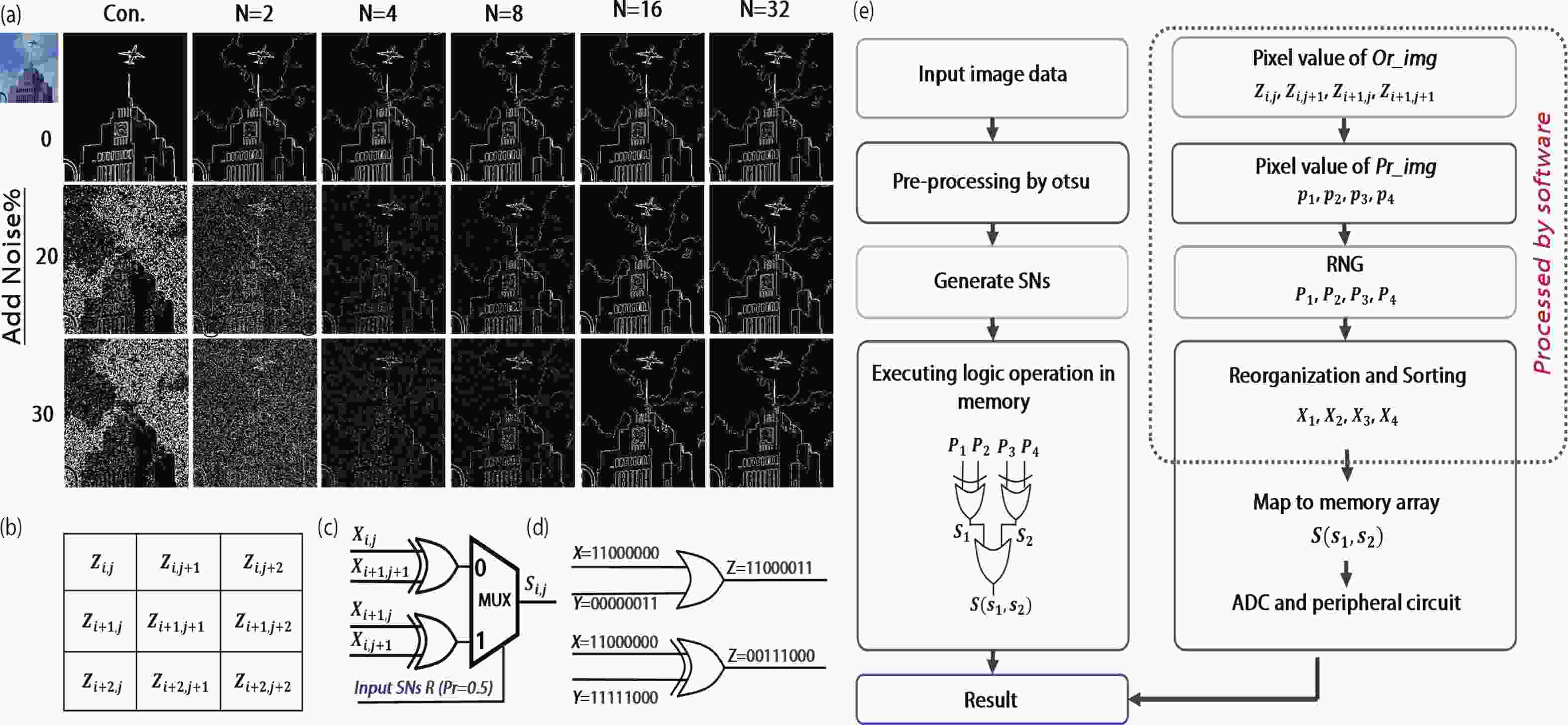
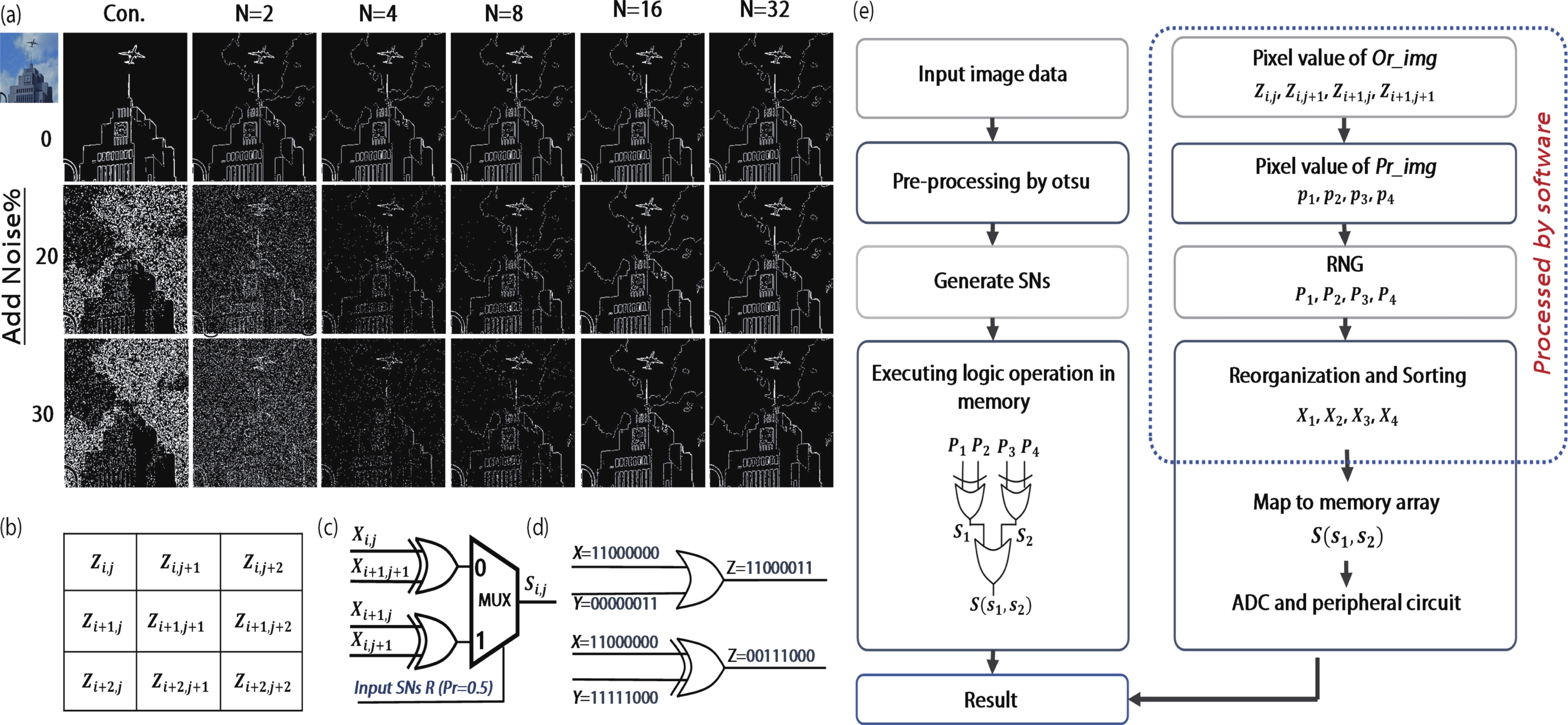
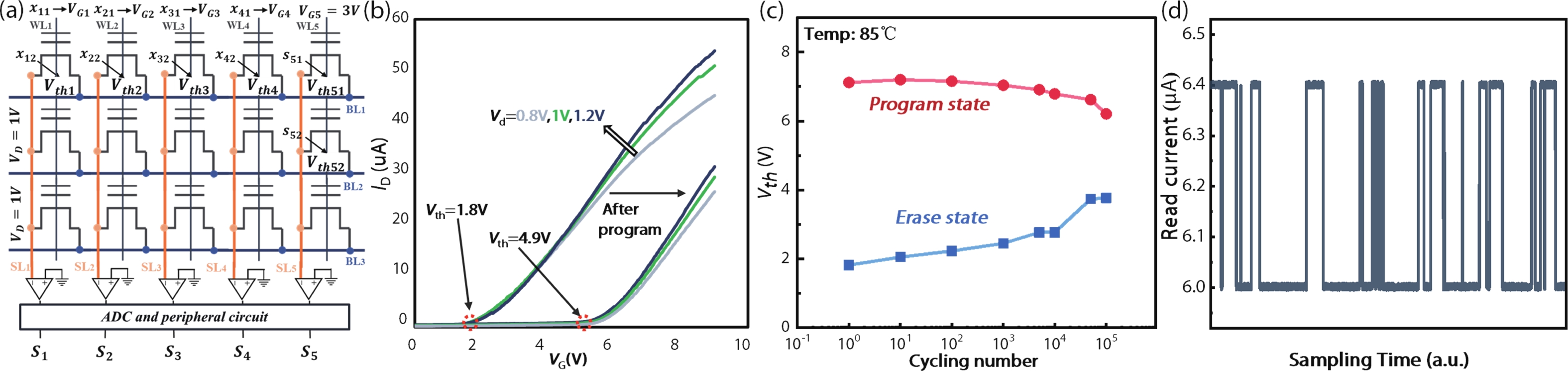
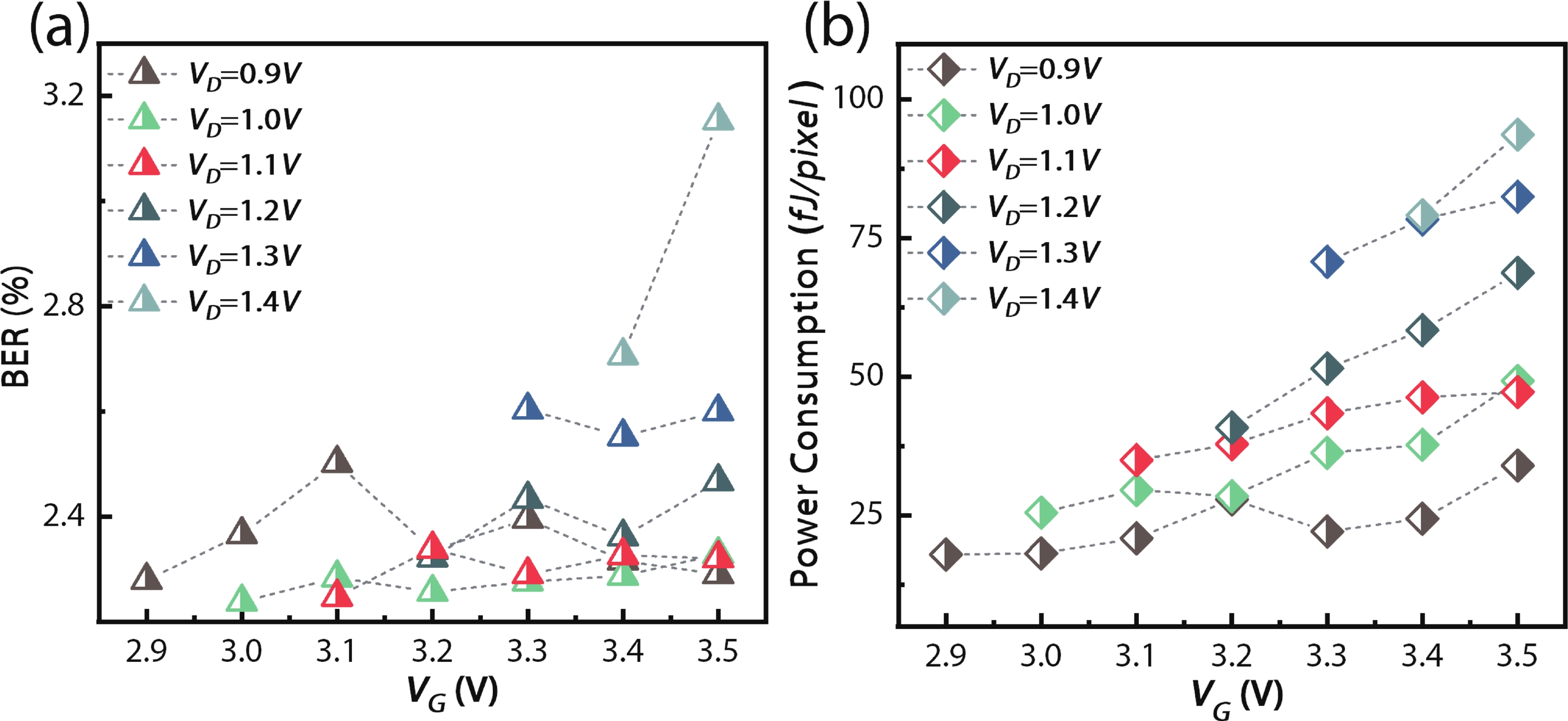
The “memory wall” of traditional von Neumann computing systems severely restricts the efficiency of data-intensive task execution, while in-memory computing (IMC) architecture is a promising approach to breaking the bottleneck. Although variations and instability in ultra-scaled memory cells seriously degrade the calculation accuracy in IMC architectures, stochastic computing (SC) can compensate for these shortcomings due to its low sensitivity to cell disturbances. Furthermore, massive parallel computing can be processed to improve the speed and efficiency of the system. In this paper, by designing logic functions in NOR flash arrays, SC in IMC for the image edge detection is realized, demonstrating ultra-low computational complexity and power consumption (25.5 fJ/pixel at 2-bit sequence length). More impressively, the noise immunity is 6 times higher than that of the traditional binary method, showing good tolerances to cell variation and reliability degradation when implementing massive parallel computation in the array.