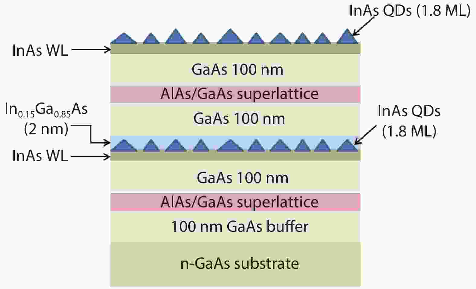
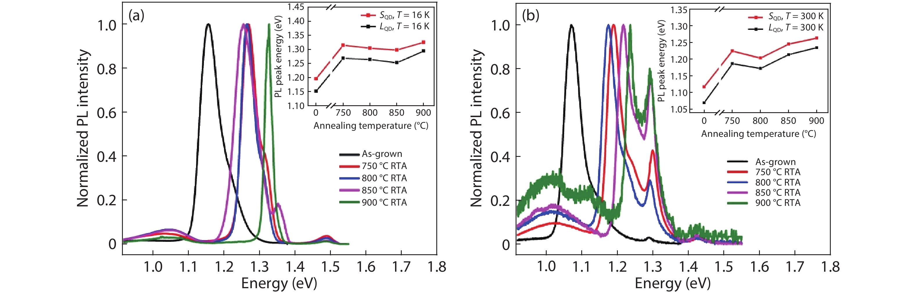
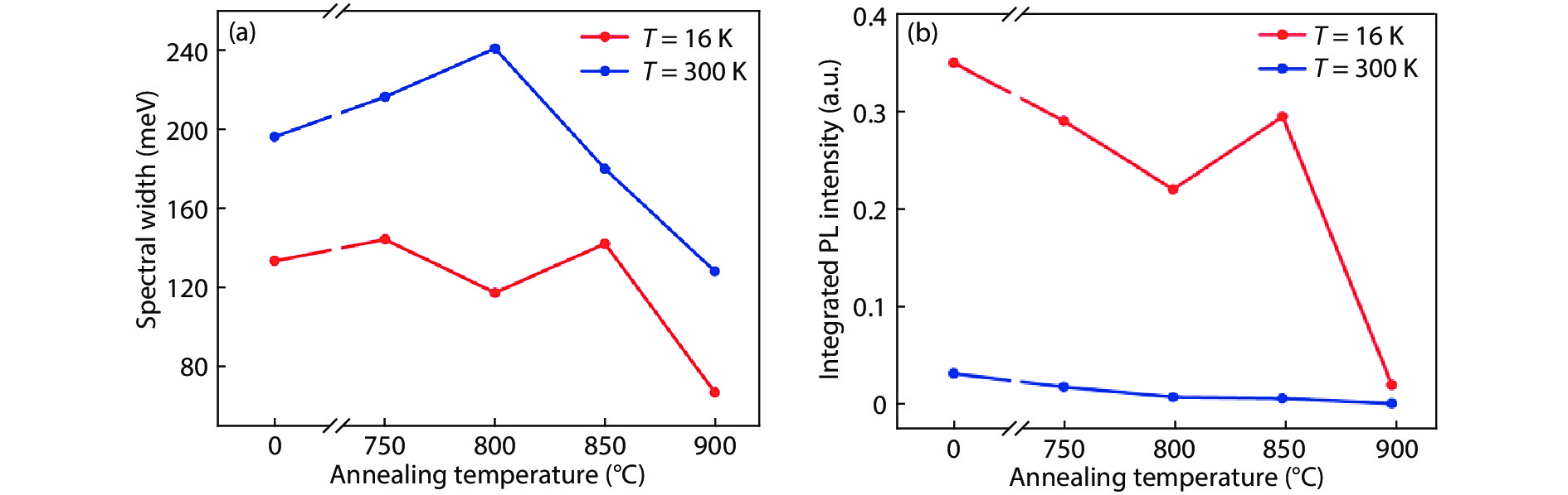
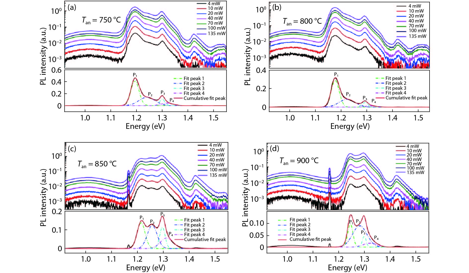
Photoluminescence (PL) test was conducted to investigate the effect of rapid thermal annealing (RTA) on the optical performance of self-assembled InAs/GaAs quantum dots (QDs) at the temperatures of 16 and 300 K. It was found that after RTA treatment, the PL spectrum of the QDs sample had a large blue-shift and significantly broadened at 300 K. Compared with the as-grown InAs QDs sample, the PL spectral width has increased by 44.68 meV in the InAs QDs sample RTA-treated at 800 °C. The excitation power-dependent PL measurements showed that the broadening of the PL peaks of the RTA-treated InAs QDs should be related to the emission of the ground state (GS) of different-sized InAs QDs, the InAs wetting layer (WL) and the In0.15Ga0.85As strain reduction layer (SRL) in the epitaxial InAs/GaAs layers.


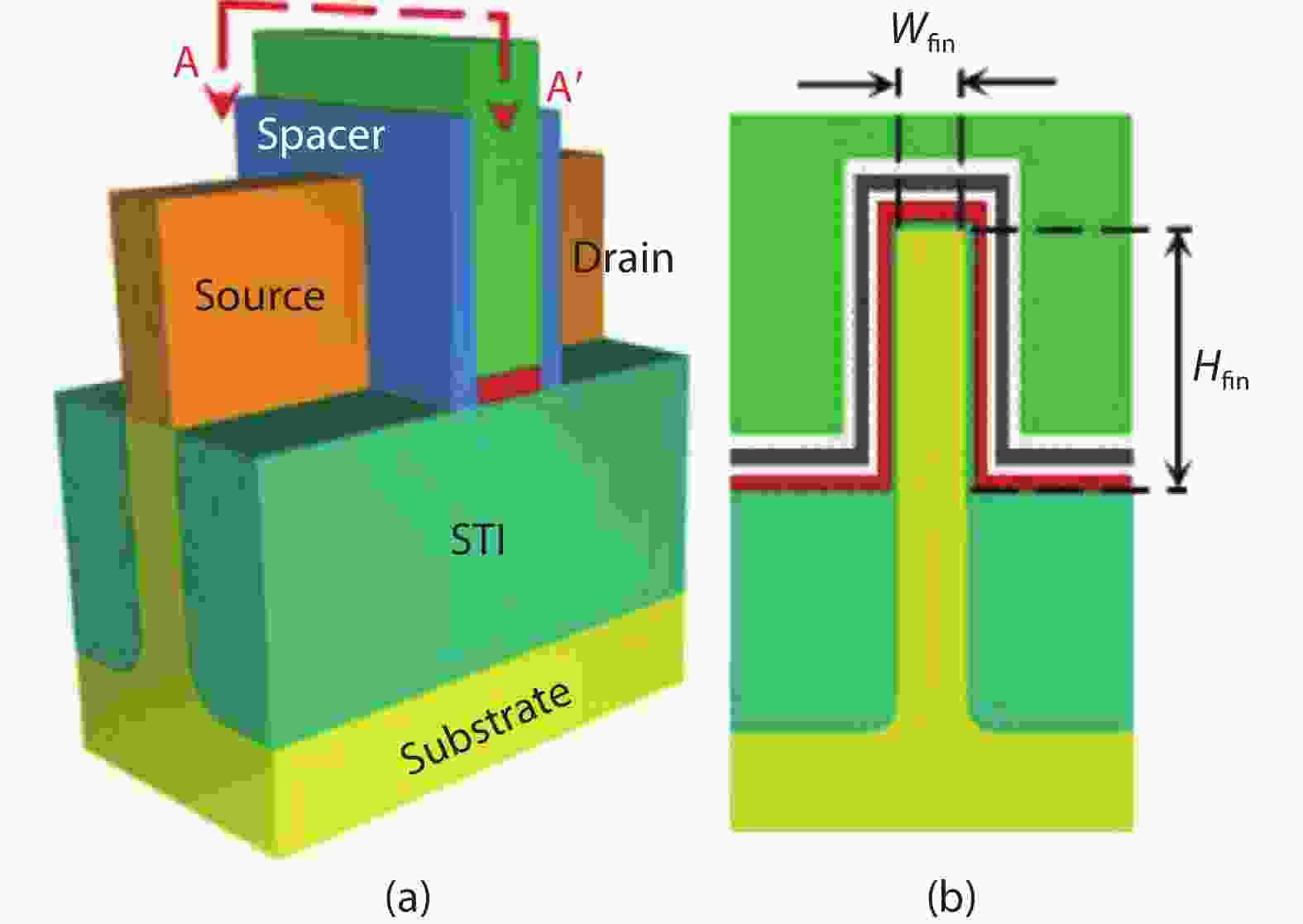
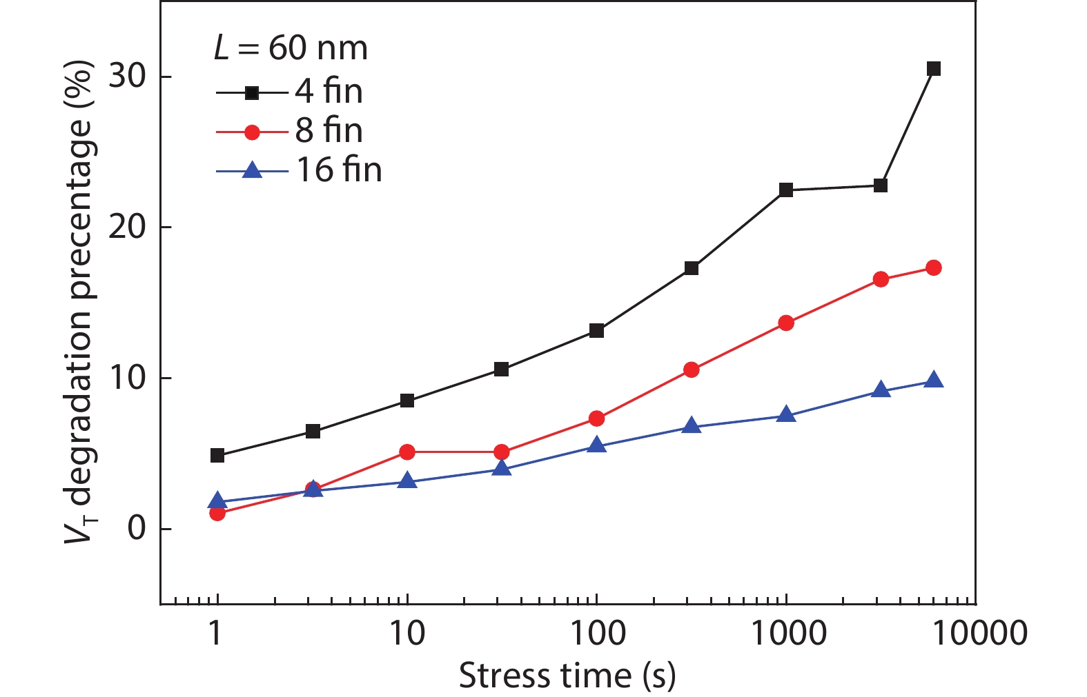
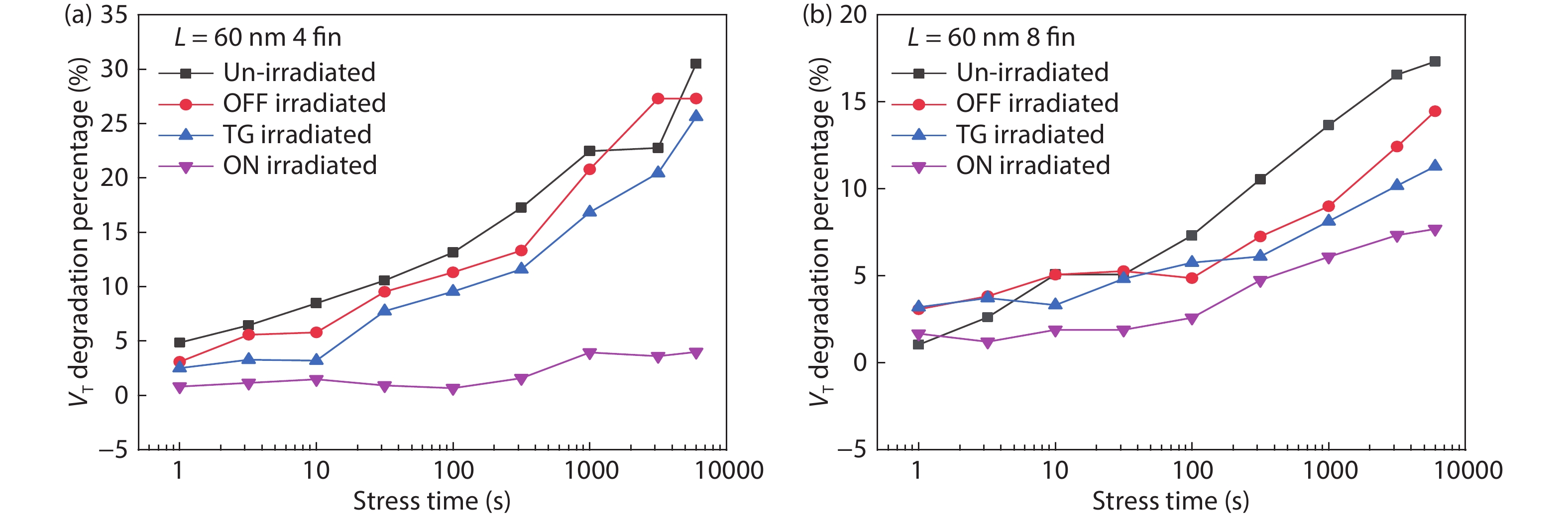
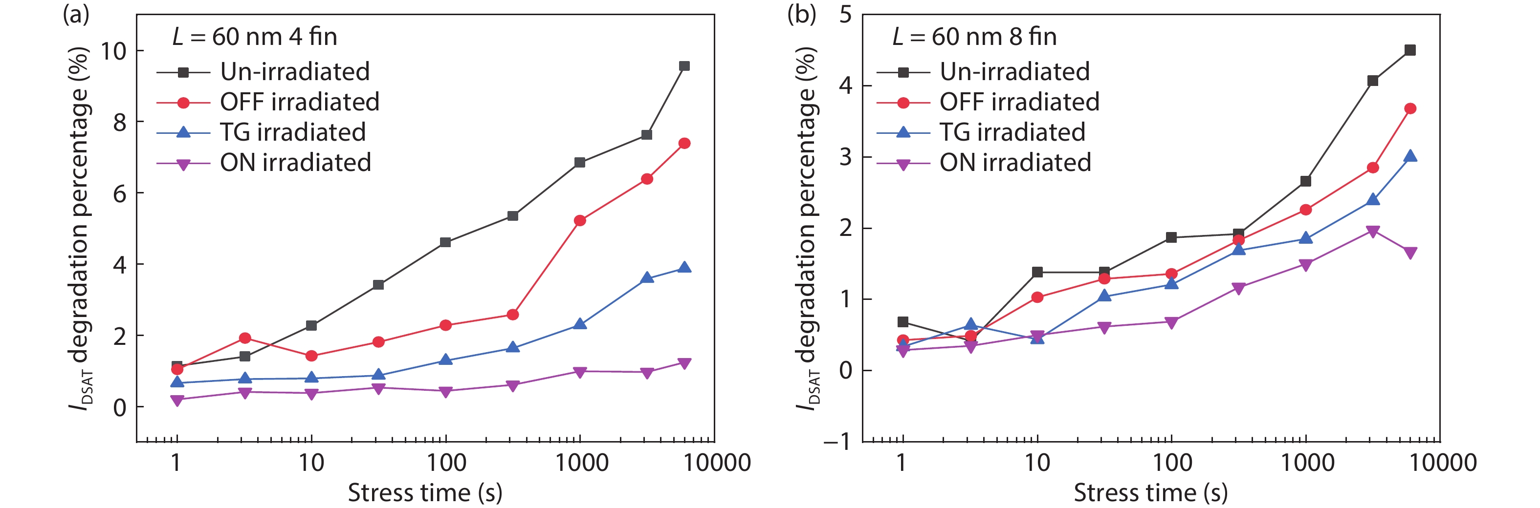
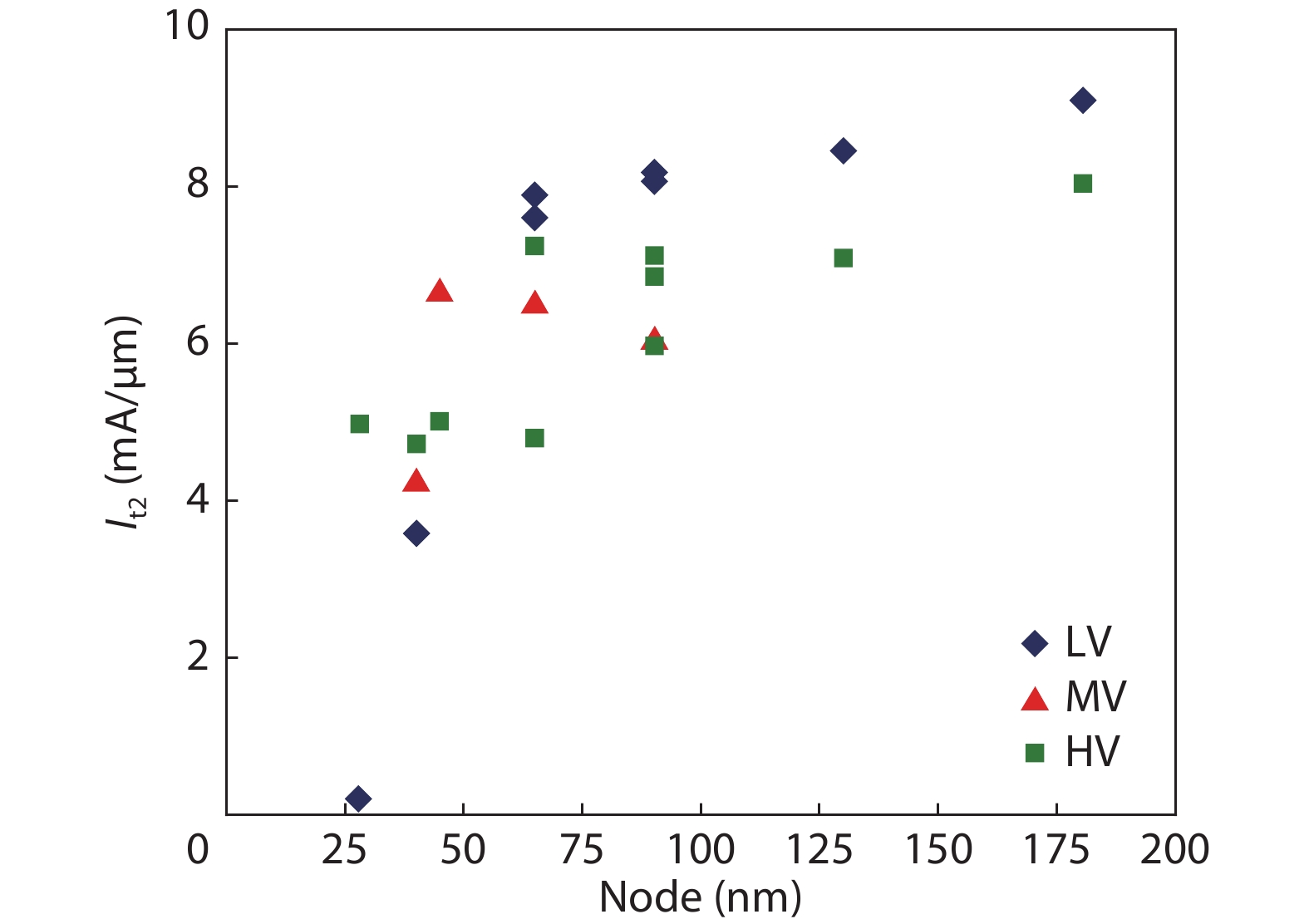
We investigate the hot carrier injection effect (HCI) and how X-ray radiation impacts the HCI of 22-nm nFinFETs as a function of device geometry and irradiation bias conditions in this paper. In the HCI test, the degradation of threshold voltage and saturation current decreases with the increase of fin number, which means that HCI weakens when the fin number increases. The reason is attributed to the coupling effect between fins. Moreover, irradiation is shown to weaken the degradation during the subsequent hot carrier test. The influence of irradiation on HCI is more obvious with ON bias than that of OFF bias and transmission gate bias. It is supposed that the Si–H bonds can be broken by irradiation before the HCI test, which is one reason for the irradiation influence on HCI. Besides, trapped charges are generated in the shallow trench isolation by the radiation, which could reduce the channel electric field, and then weaken the HCI.


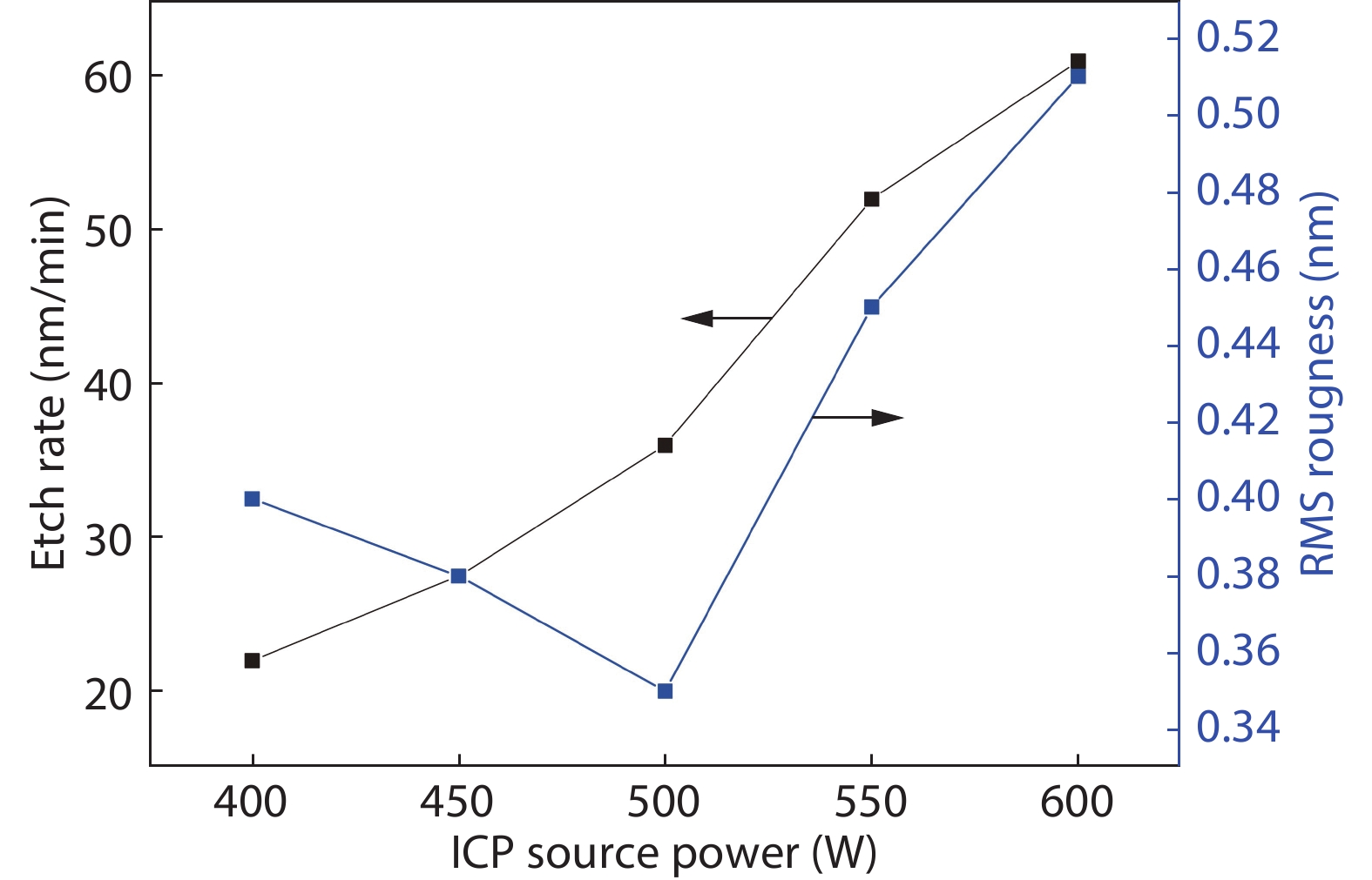
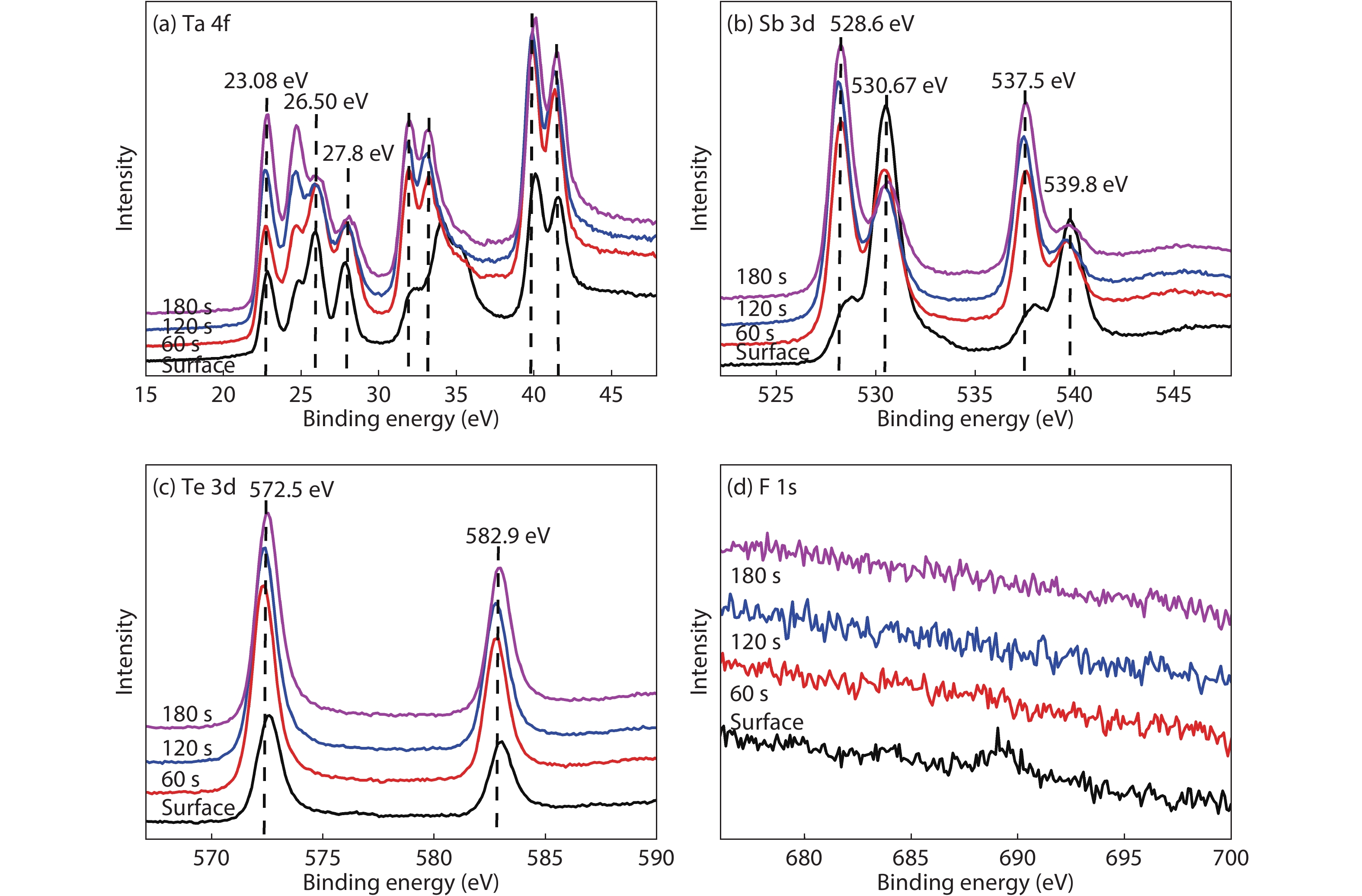
Compared to the conventional phase change materials, the new phase change material Ta-Sb2Te3 has the advantages of excellent data retention and good material stability. In this letter, the etching characteristics of Ta-Sb2Te3 were studied by using CF4/Ar. The results showed that when CF4/Ar = 25/25, the etching power was 600 W and the etching pressure was 2.5 Pa, the etching speed was up to 61 nm/min. The etching pattern of Ta-Sb2Te3 film had a smooth side wall and good perpendicularity (close to 90°), smooth surface of the etching (RMS was 0.51nm), and the etching uniformity was fine. Furthermore, the mechanism of this etching process was analyzed by X-ray photoelectron spectroscopy (XPS). The main damage mechanism of ICP etching in CF4/Ar was studied by X-ray diffraction (XRD).


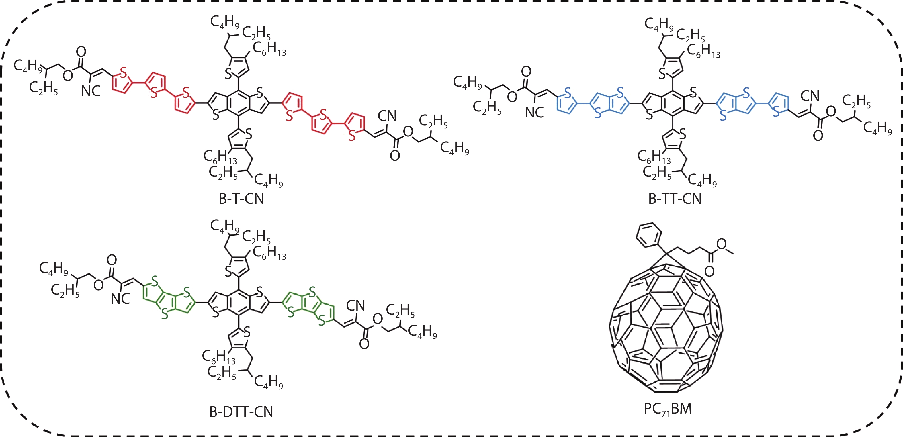
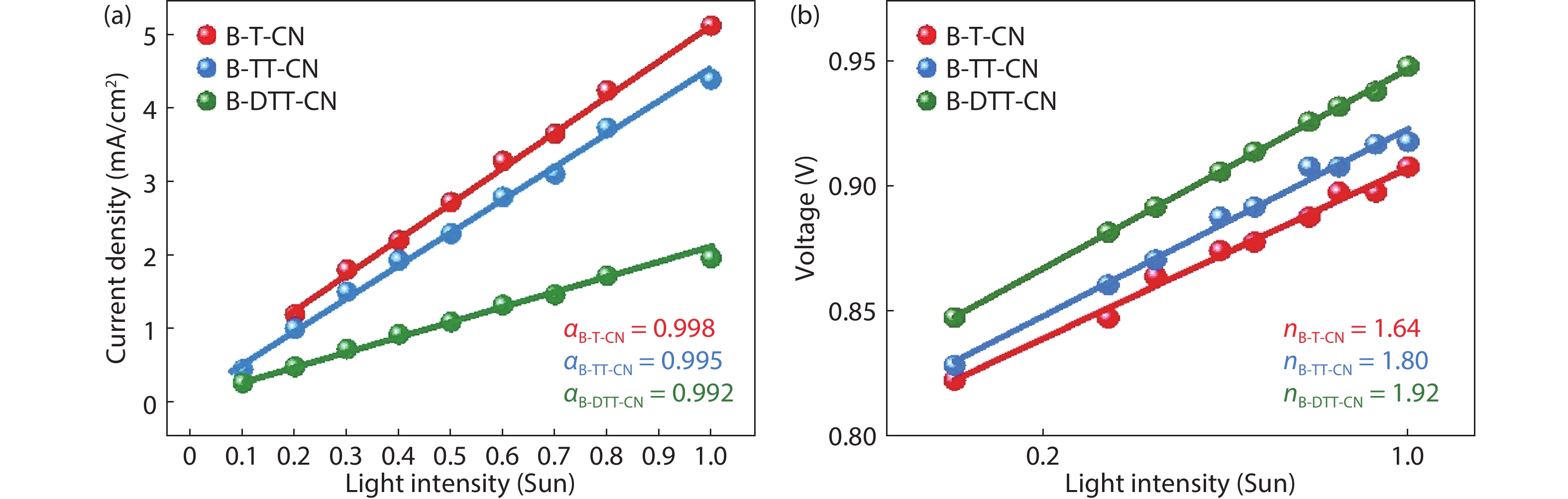
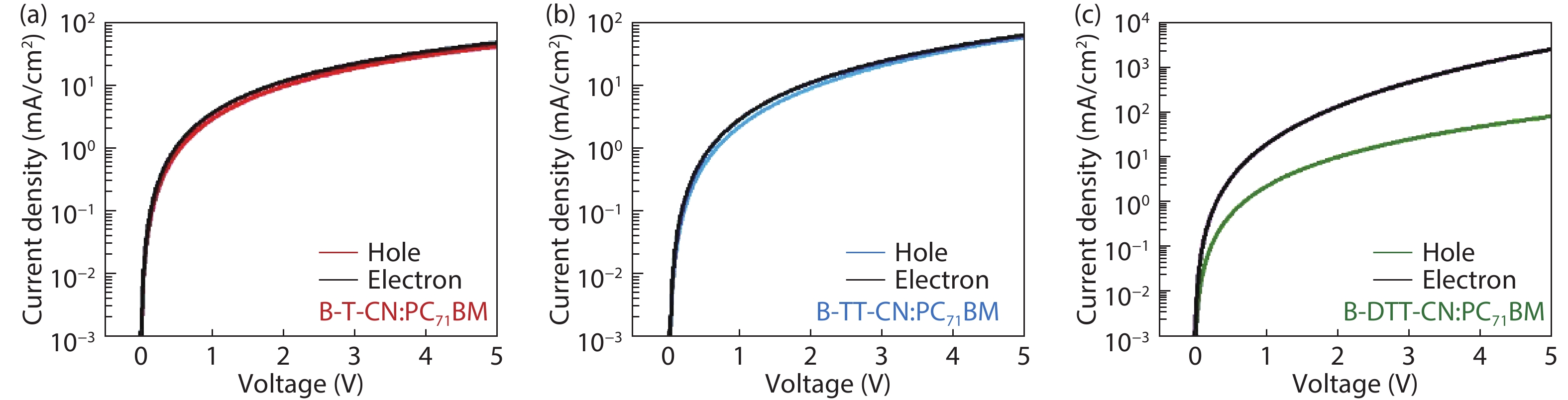
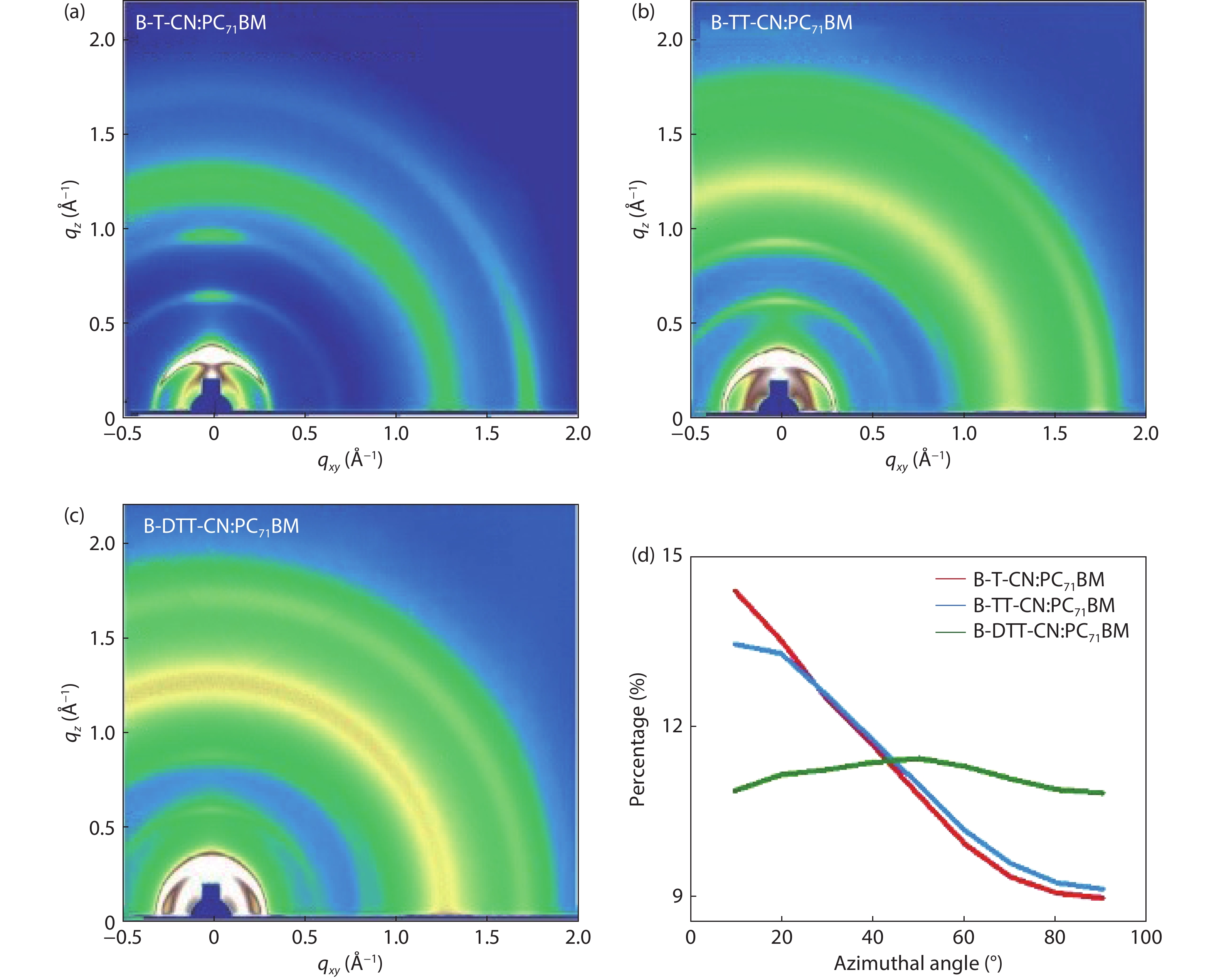
Three small molecule (SM) donors, namely B-T-CN, B-TT-CN and B-DTT-CN, with different π conjugated bridges were synthesized in this research. Interestingly, with the conjugated fused rings of the π linking bridge increasing, the SM HOMO levels exhibit a decline tendency with –5.27 eV for B-T-CN, –5.31 eV for B-TT-CN and –5.40 eV for B-DTT-CN. After blending the SM donors with the fullerene acceptor PC71BM, the all SM organic solar cells (OSCs) achieved high Vocs of 0.90 to 0.96 V. However, the phase separation morphology and molecule stacking are also unexpectedly changed together with the enhancement of conjugated degree of π bridges, resulting in a lower power conversion efficiency (PCE) for the B-DTT-CN:PC71BM device. Our results demonstrate and provide a useful way to enhance OSC Voc and the morphology needs to be further optimized.


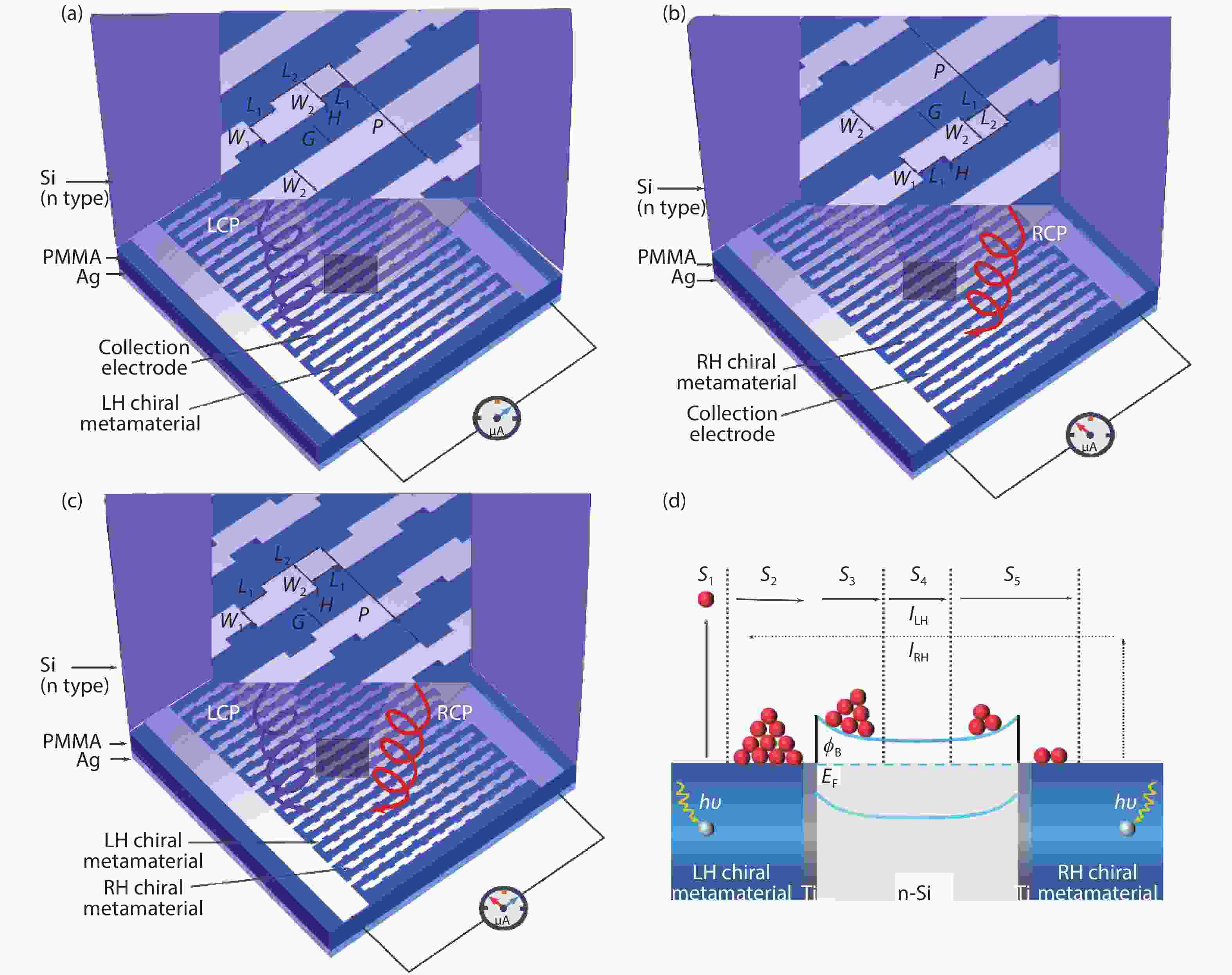
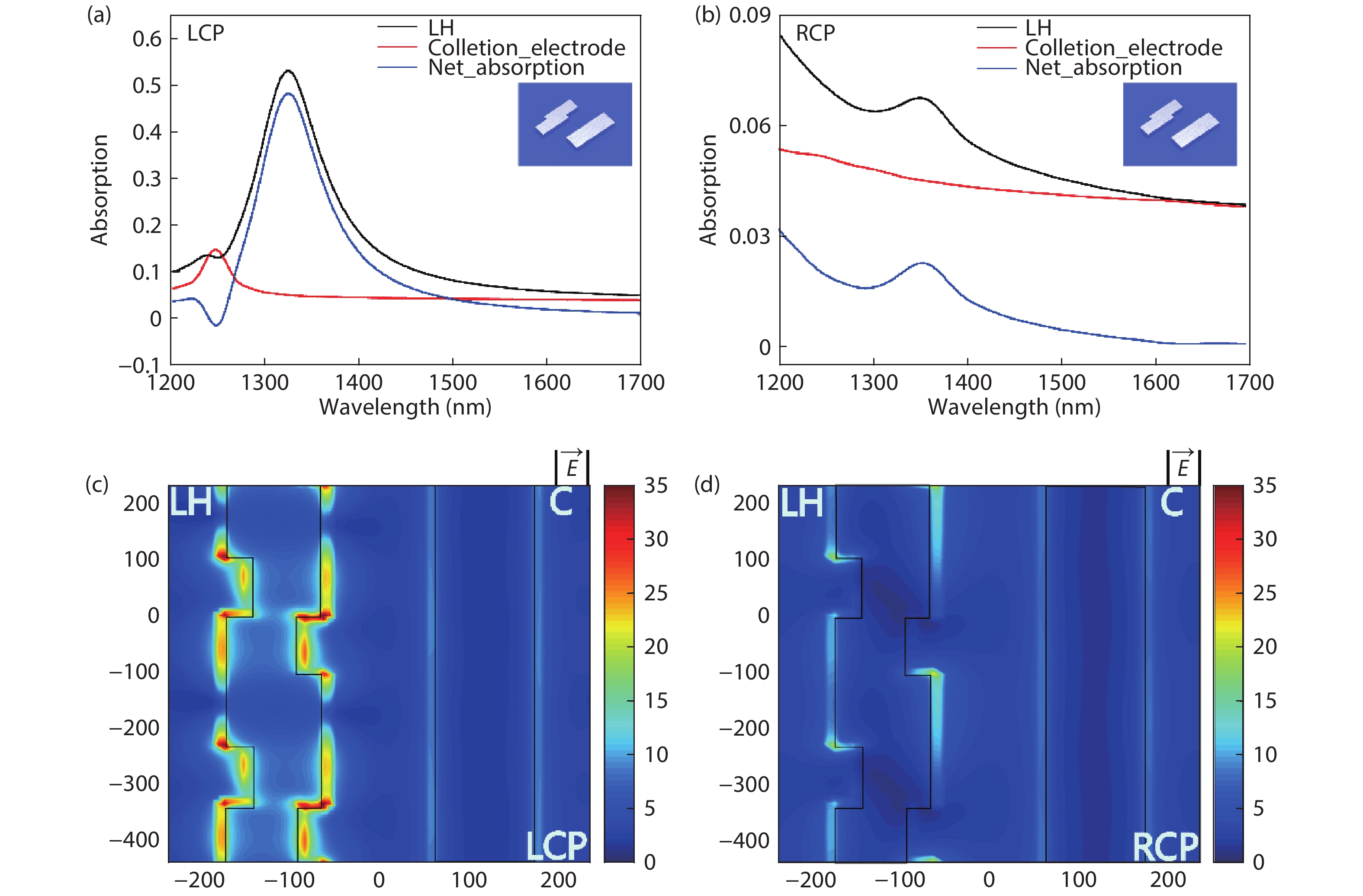
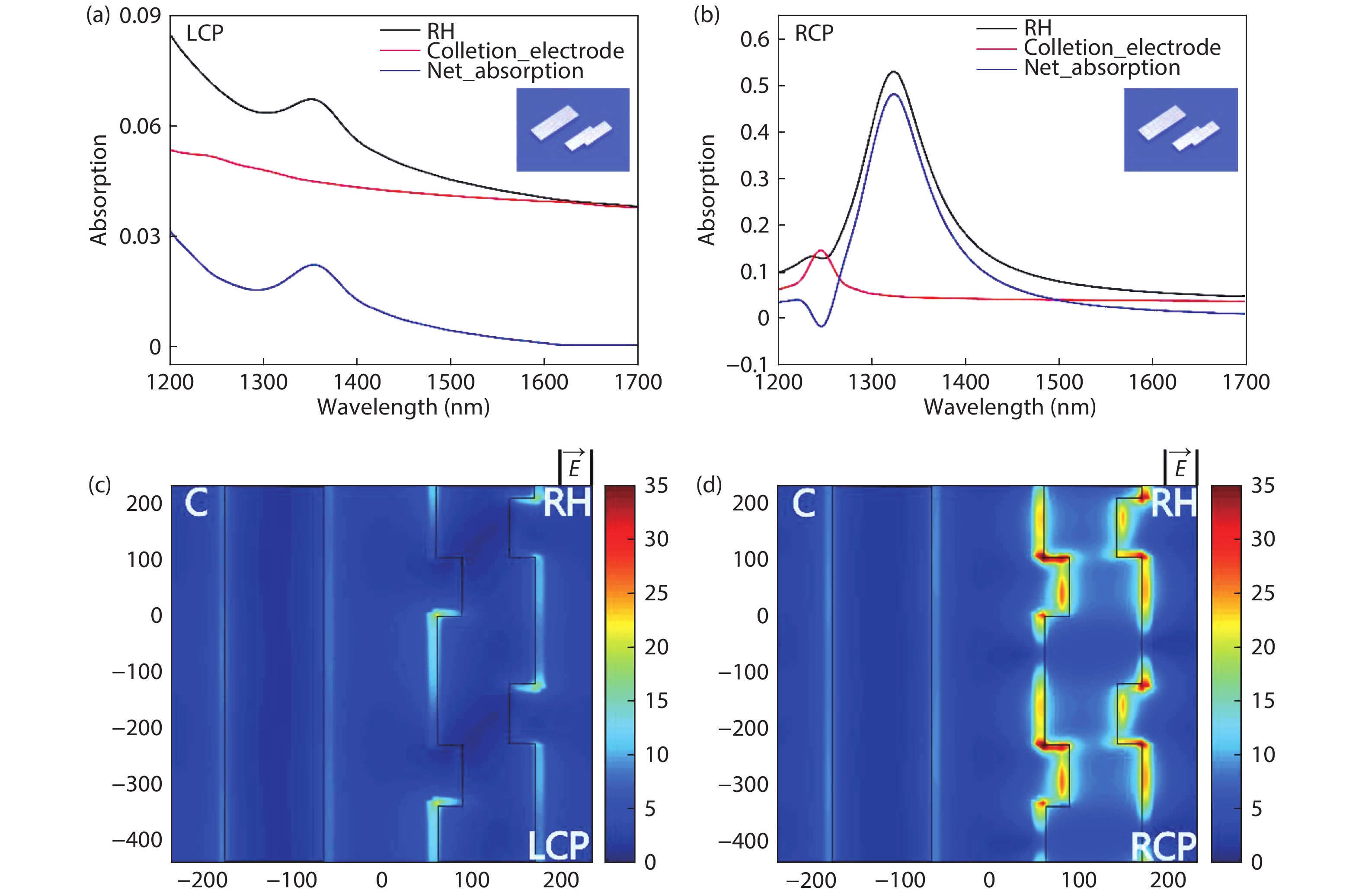
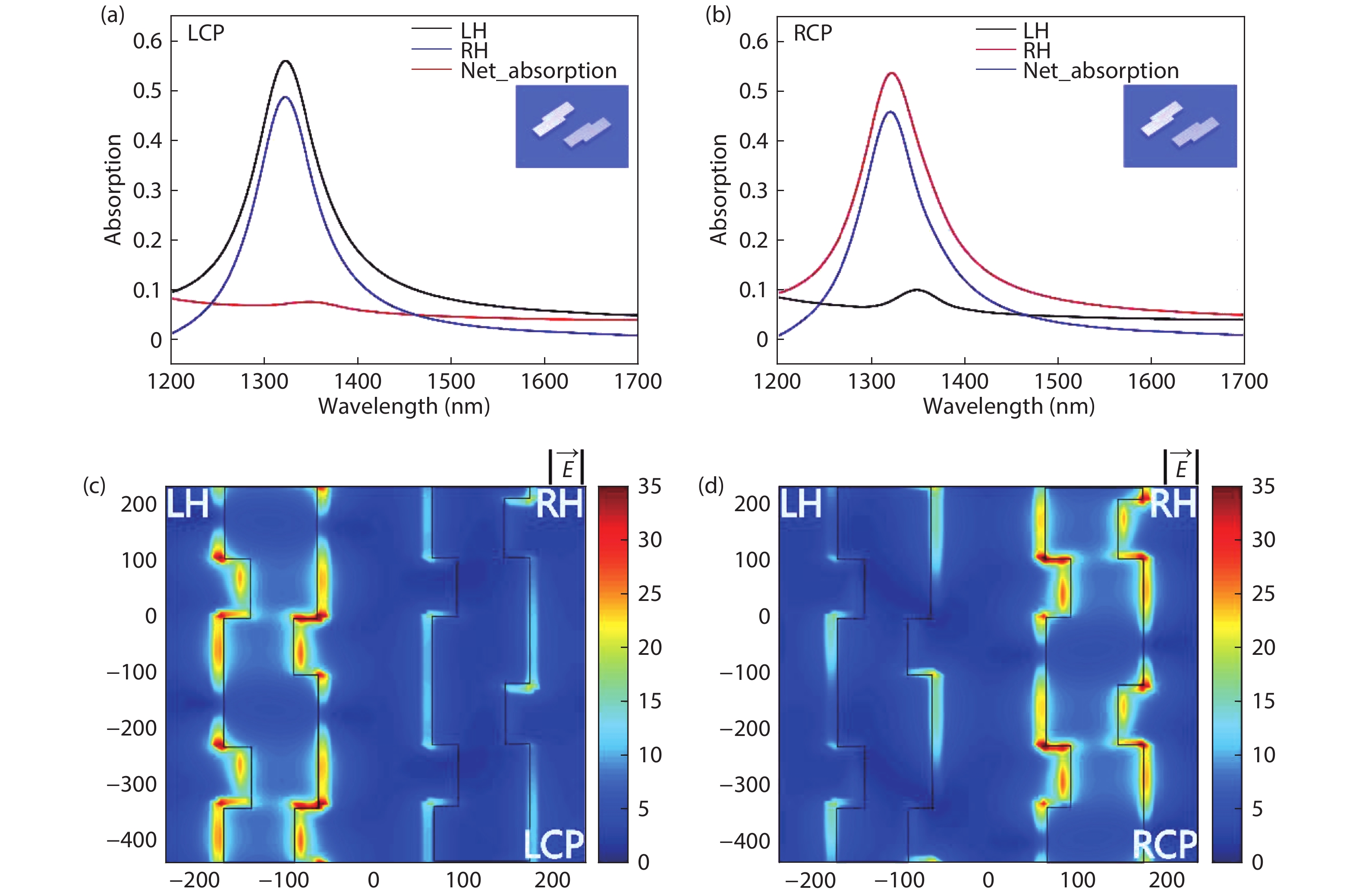
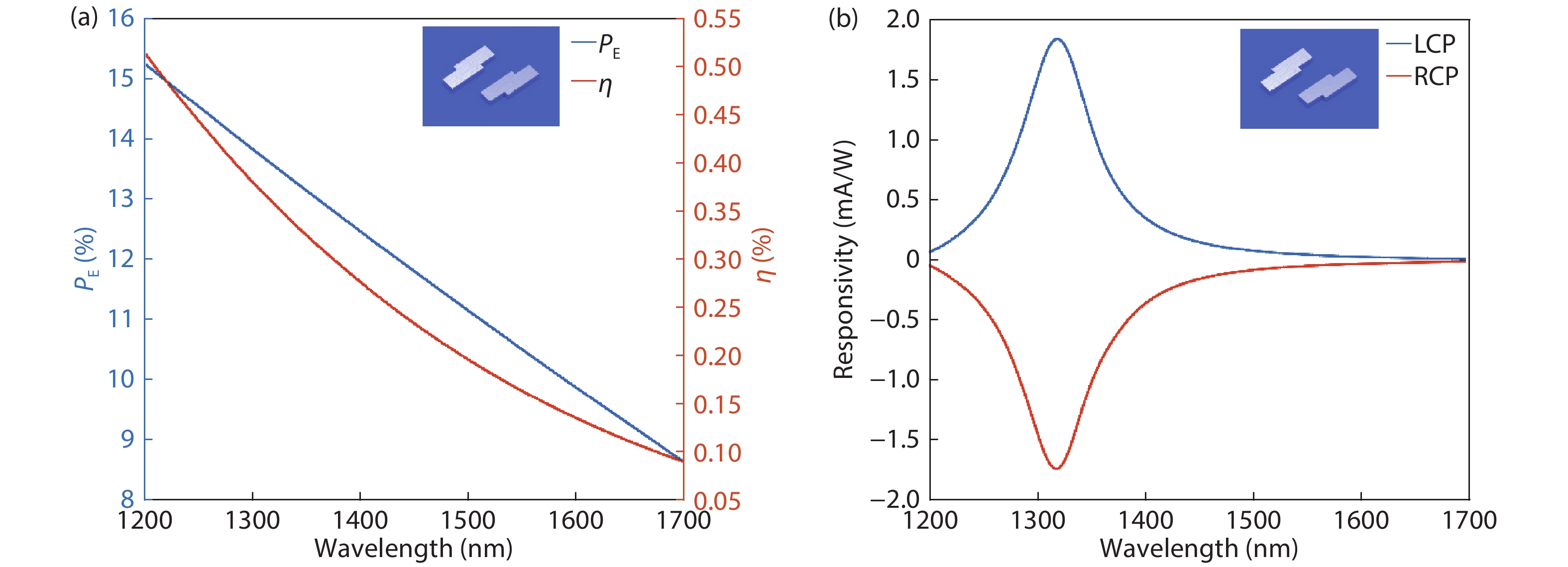
Circularly polarized light (CPL) has been given great attention because of its extensive application. While several devices for CPL detection have been studied, their performance is affected by the magnitude of photocurrent. In this paper, a self-powered photodetector based on hot electrons in chiral metamaterials is proposed and optimized. CPL can be distinguished by the direction of photocurrent without external bias owing to the interdigital electrodes with asymmetric chiral metamaterials. Distinguished by the direction of photocurrent, the device can easily detect the rotation direction of the CPL electric field, even if it only has a very weak responsivity. The responsivity of the proposed detector is near 1.9 mA/W at the wavelength of 1322 nm, which is enough to distinguish CPL. The detector we proposed has the potential for application in optical communication.


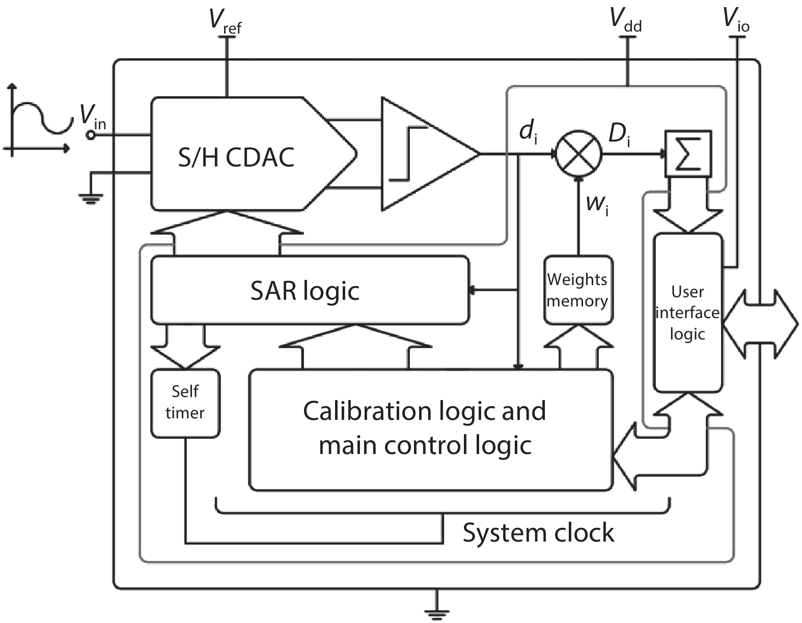
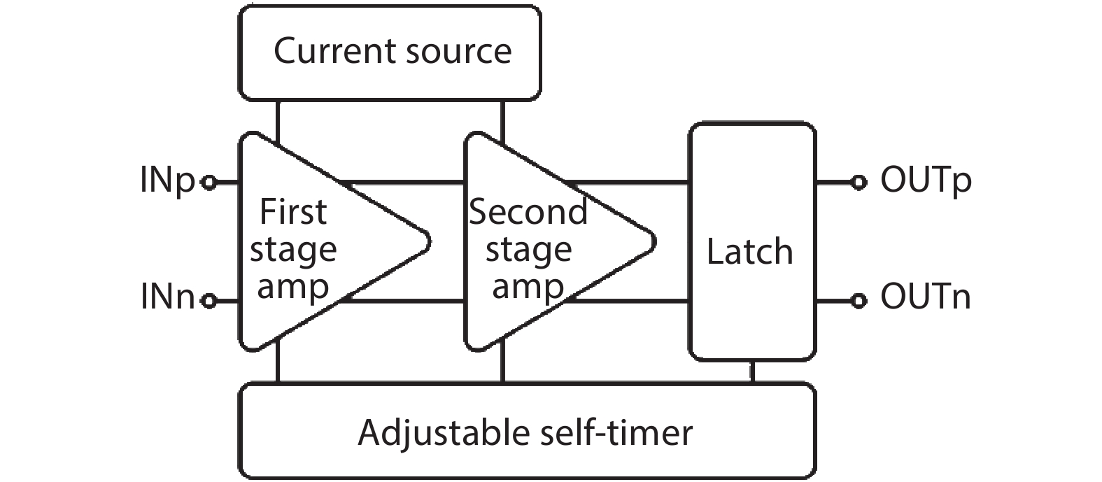
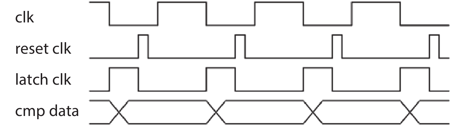
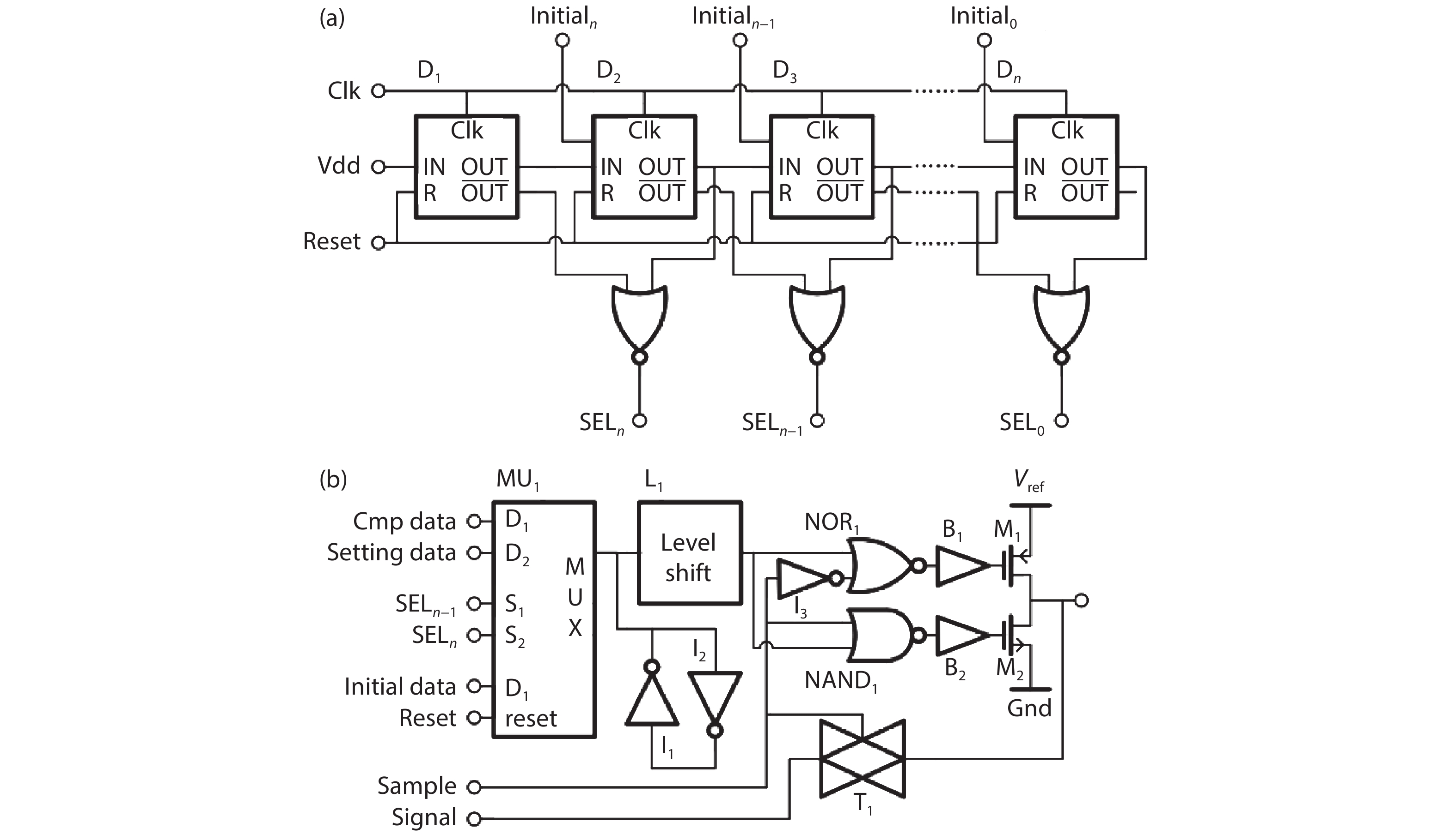
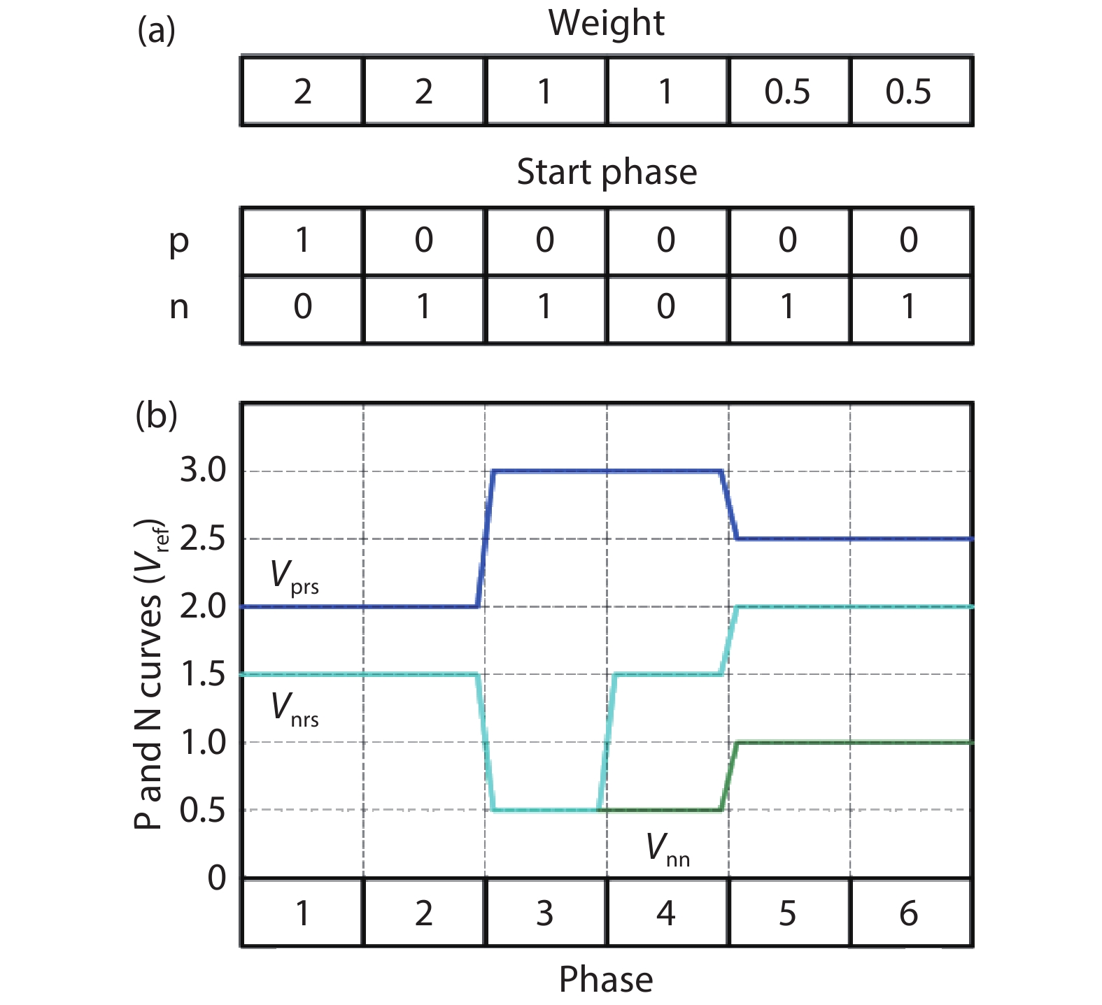
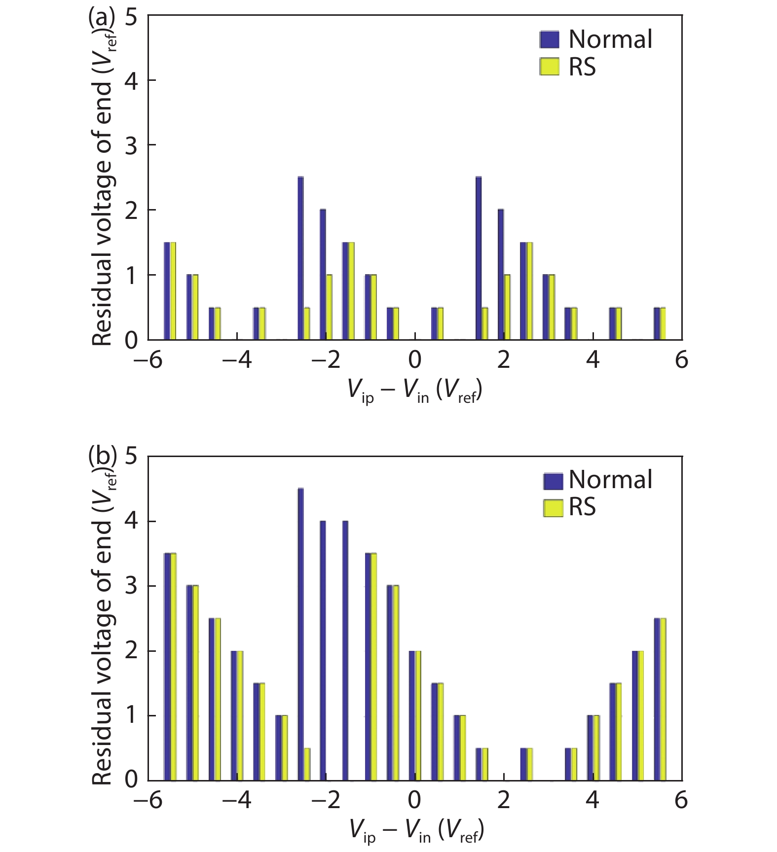
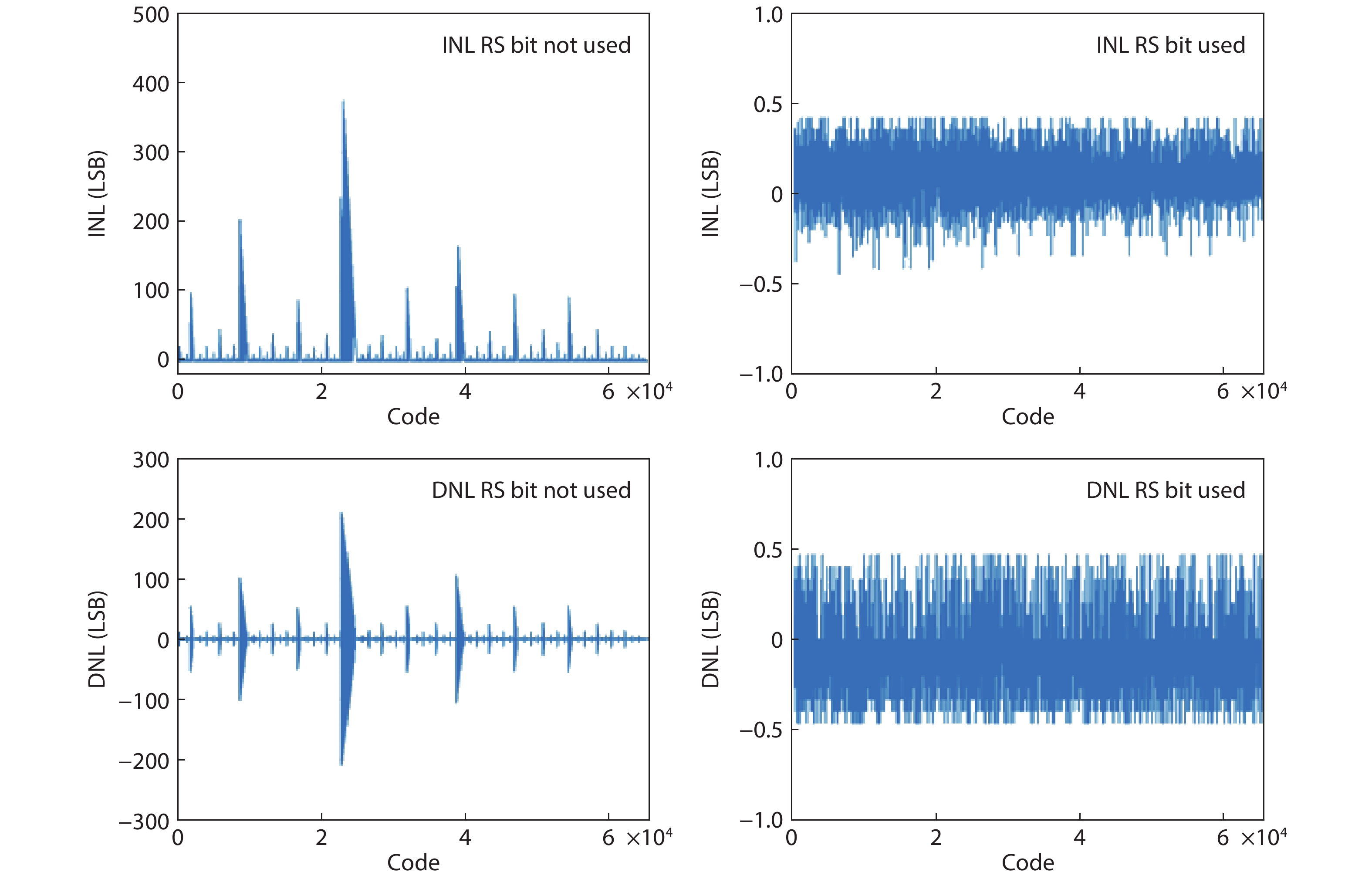
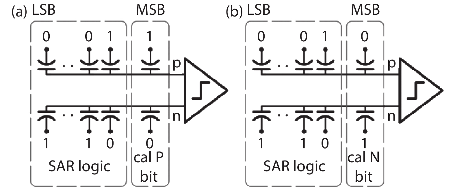
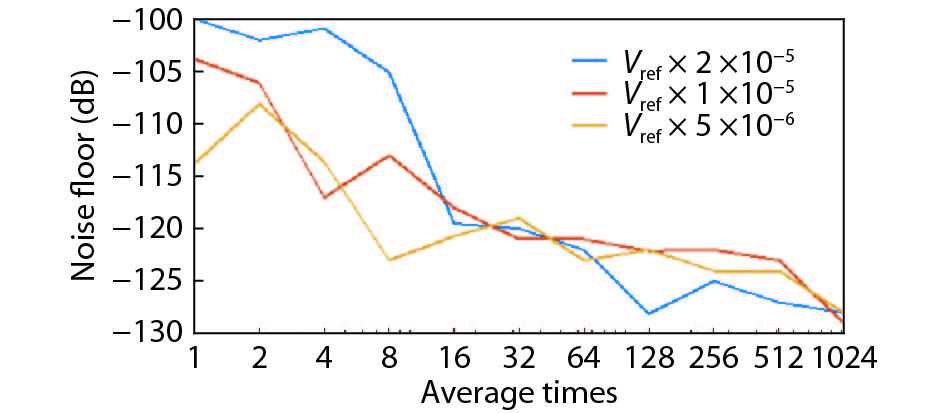
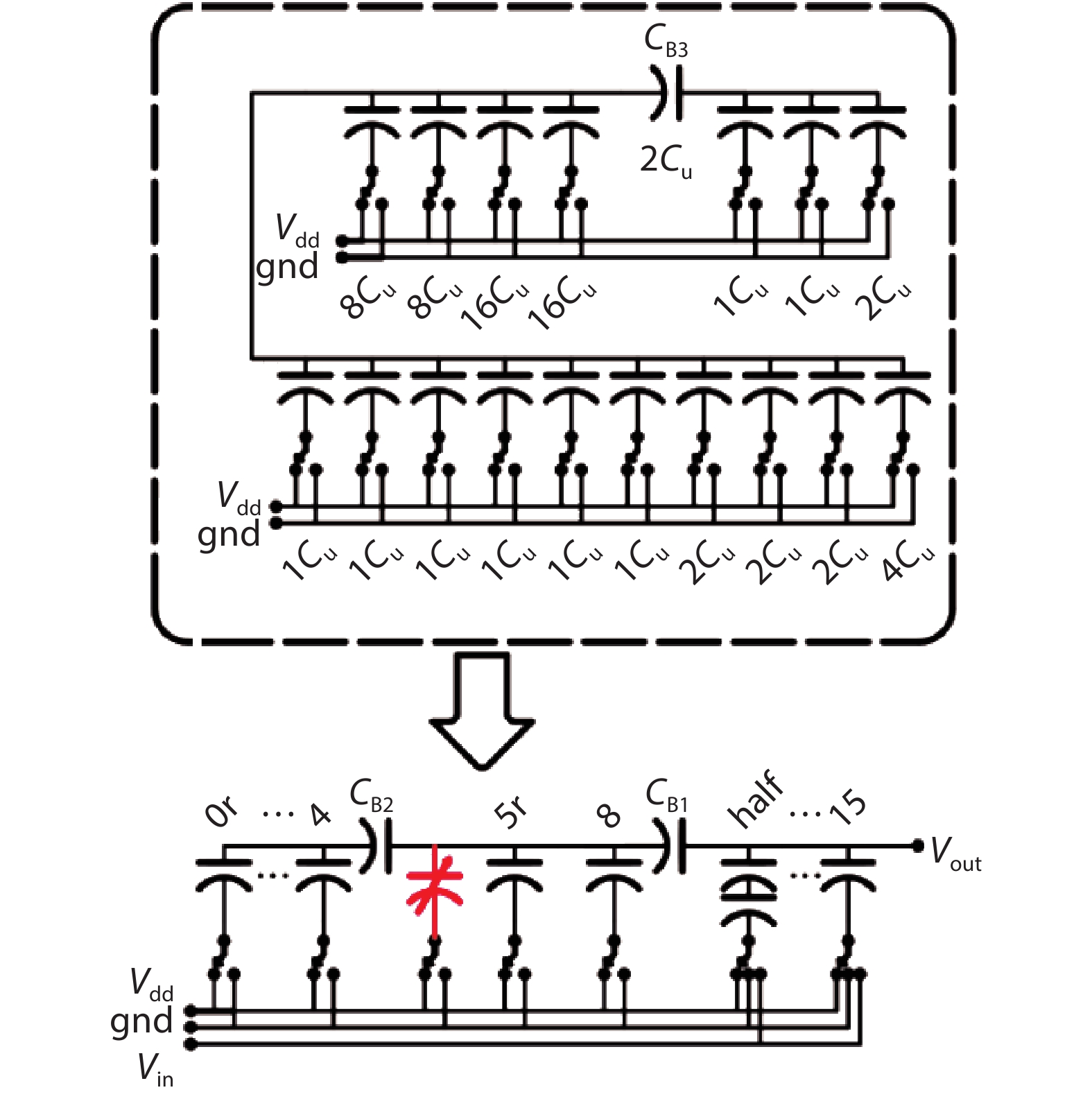
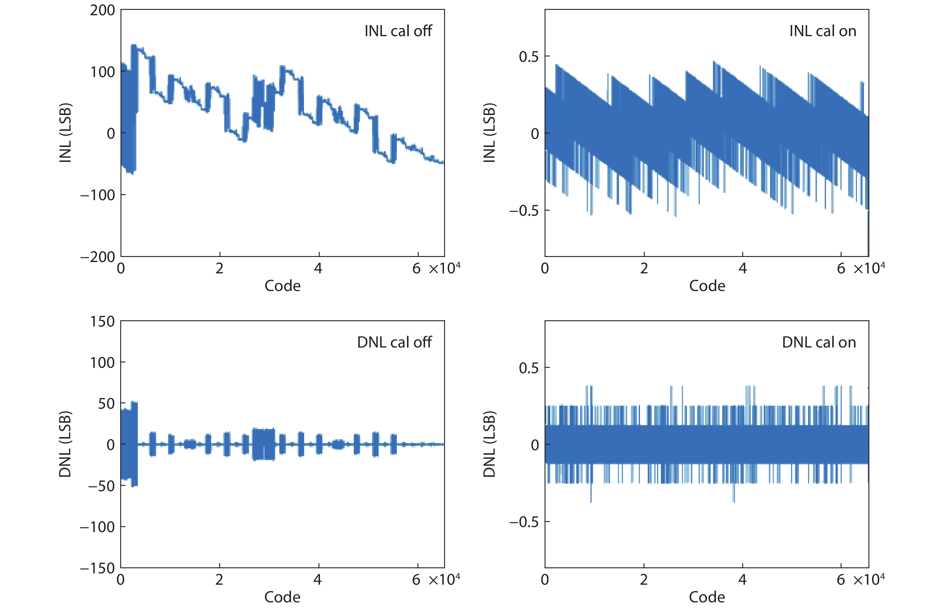
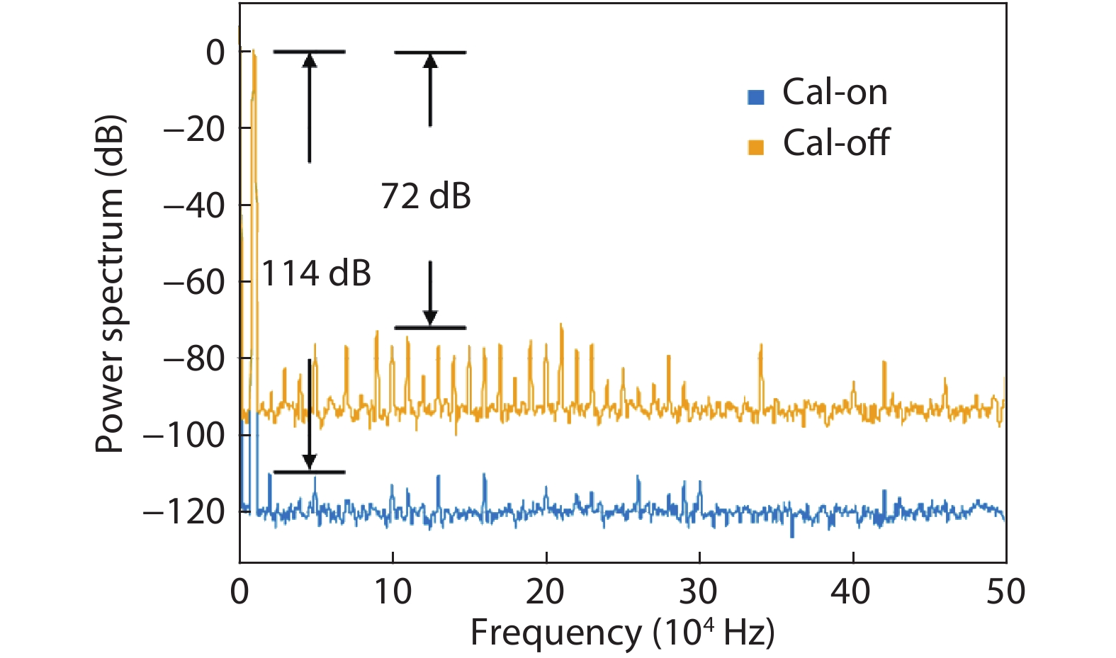
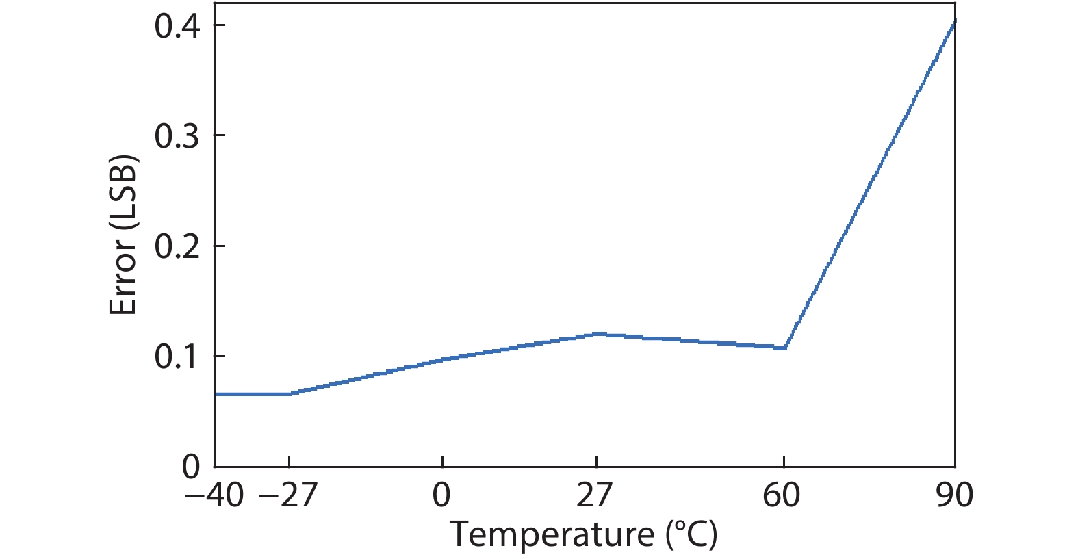
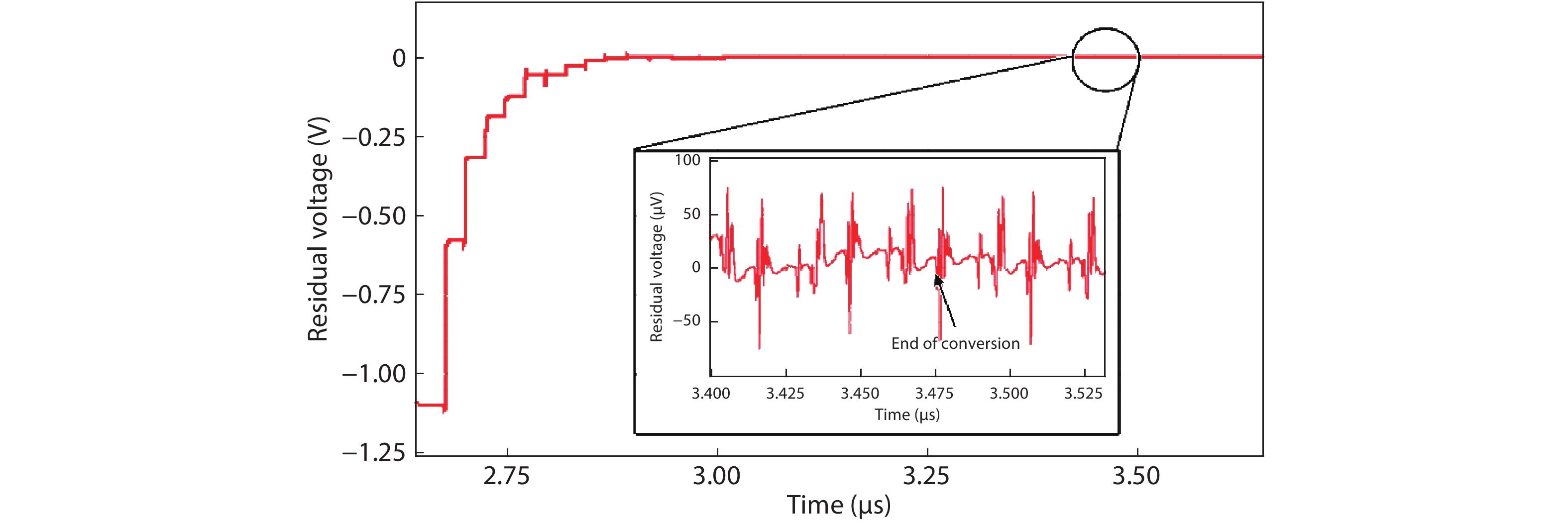
In this paper, a 16-bit 1MSPS foreground calibration successive approximation register analog-to-digital converter (SAR ADC) is developed by the CMOS 0.25 μm process. An on-chip all-digital foreground weights calibration technique integrating self-calibration weight measurement with PN port auto-balance technique is designed to improve the performance and lower the costs of the developed SAR ADC. The SAR ADC has a chip area of 2.7 × 2.4 mm2, and consumes only 100 μW at the 2.5 V supply voltage with 100 KSPS. The INL and DNL are both less than 0.5 LSB.


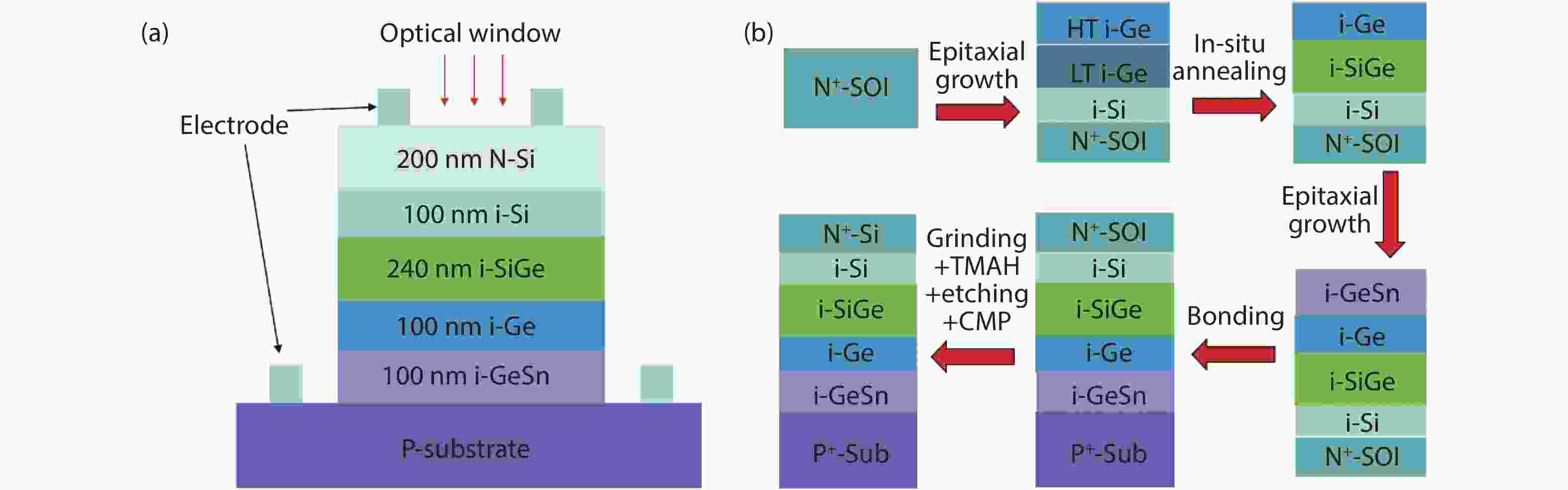
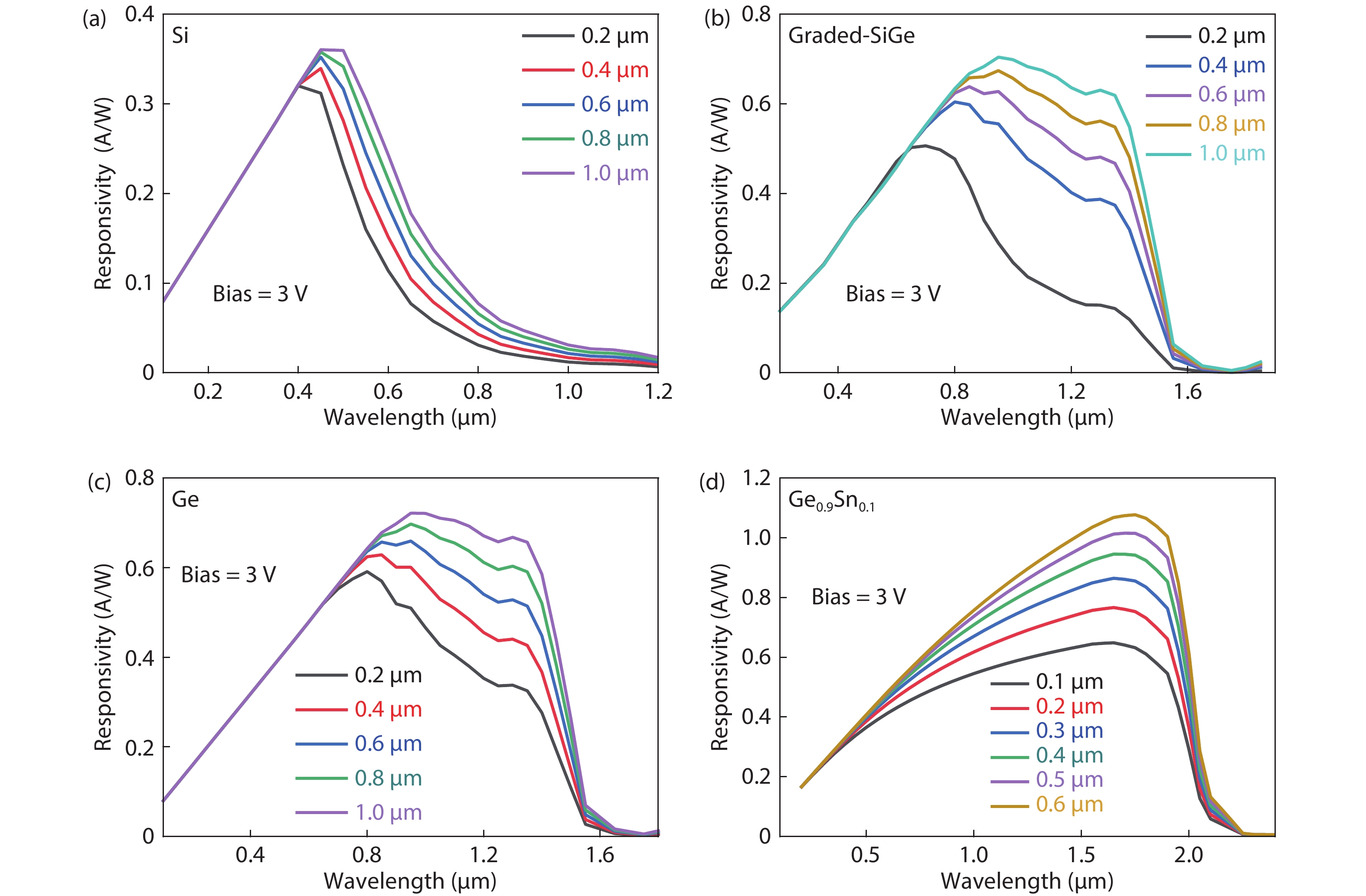
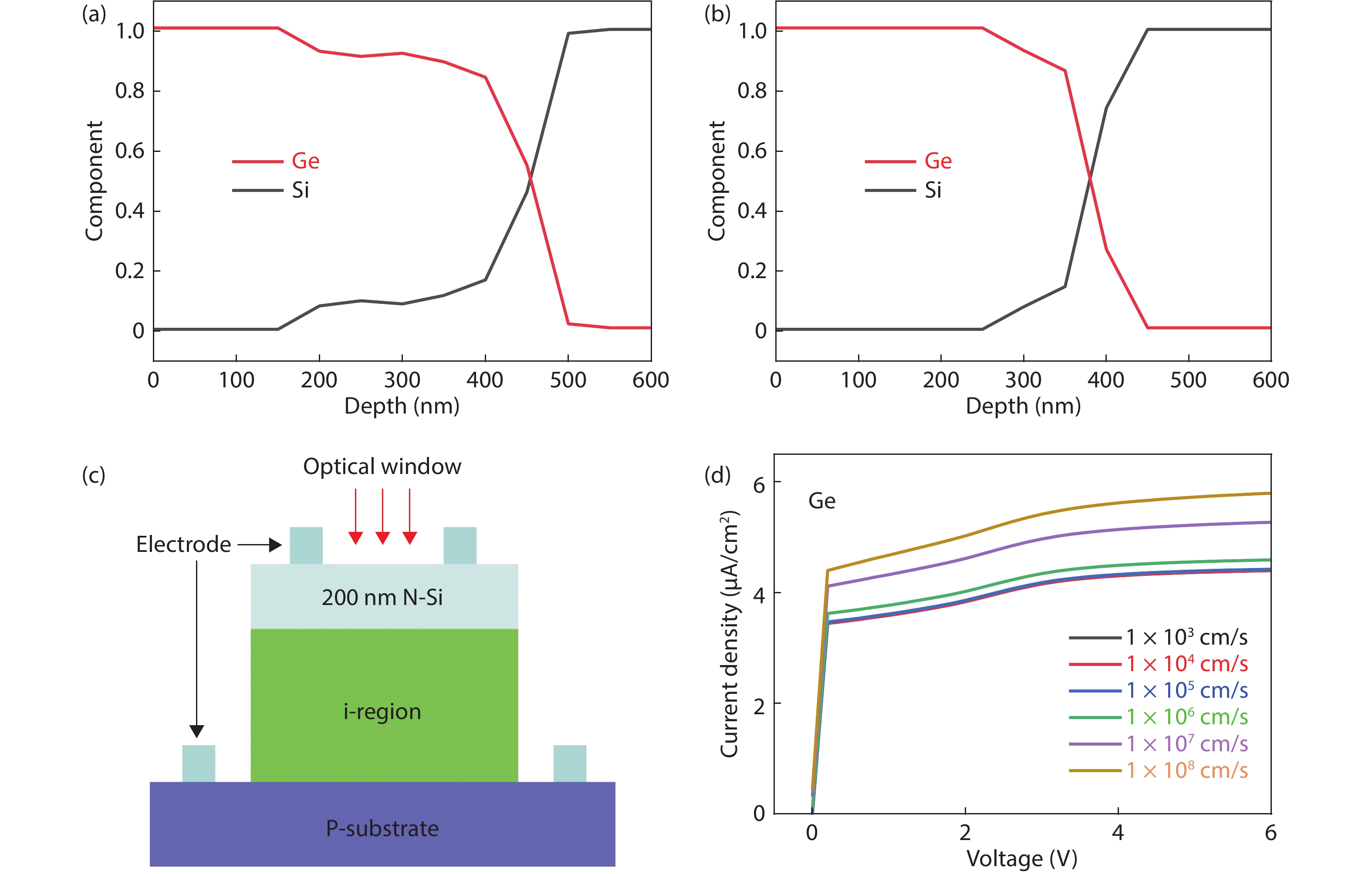
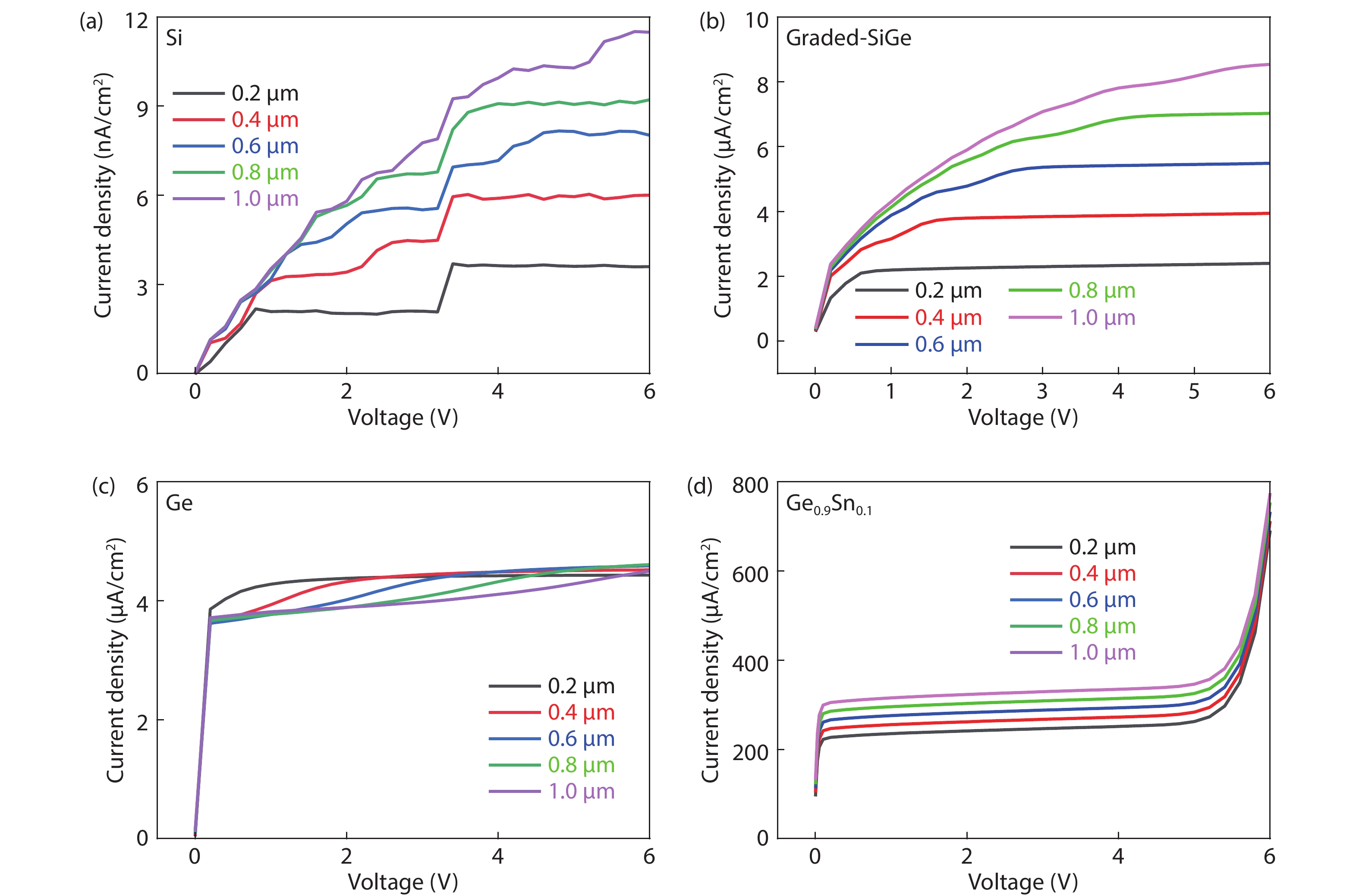
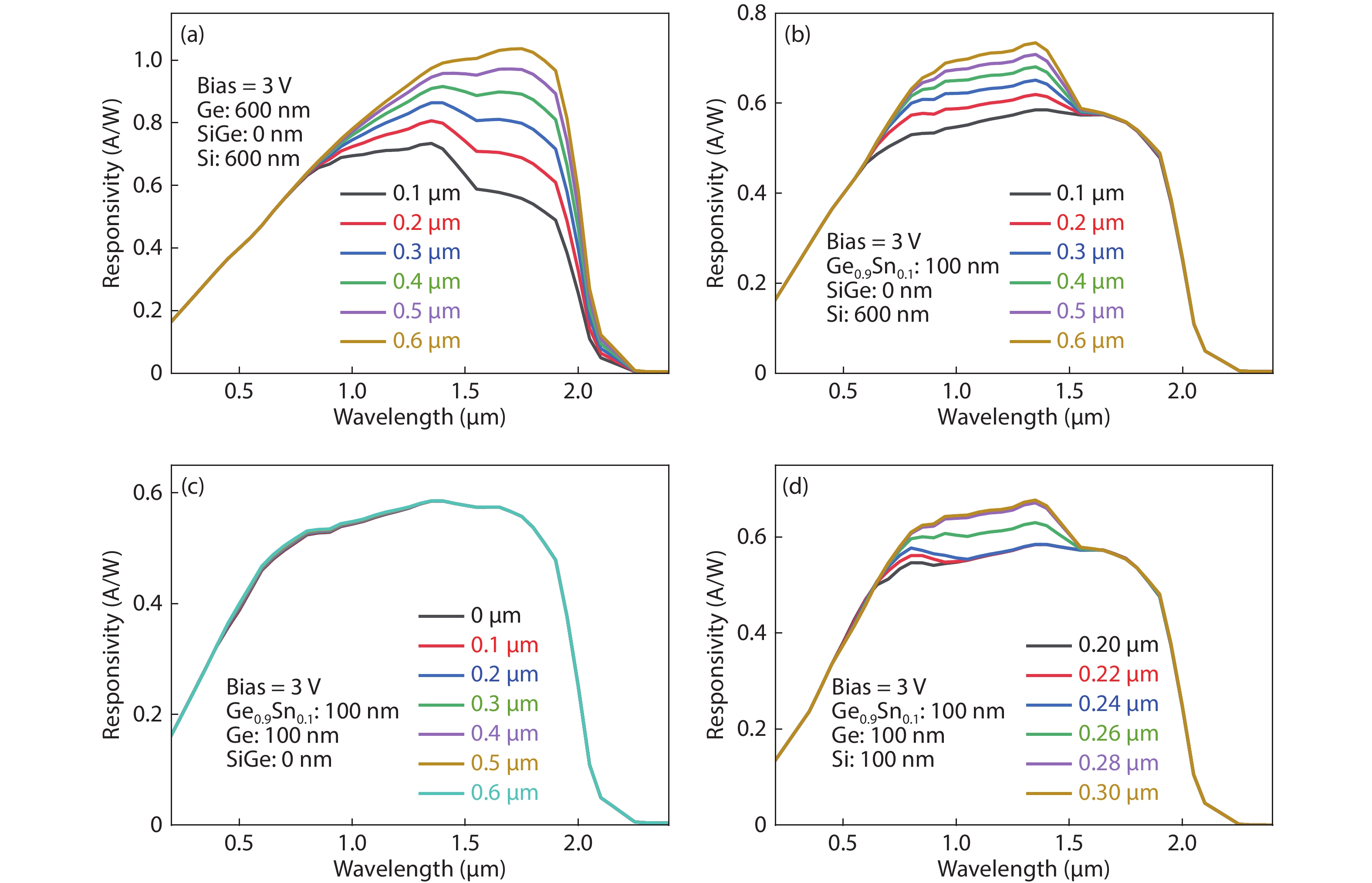
We report a theoretical study of a broadband Si/graded-SiGe/Ge/Ge0.9Sn0.1 p–i–n photodetector with a flat response based on modulating thickness of the layers in the active region. The responsivity of the photodetector is about 0.57 A/W in the range of 700 to 1800 nm. This structure is suitable for silicon-based epitaxial growth. Annealing is technically applied to form the graded-SiGe. The photodetector reaches a cut-off wavelength at ~2300 nm and a low dark-current density under 3 V reverse bias about 0.17 mA/cm2 is achieved theoretical at room temperature. This work is of great significance for silicon-based detection and communication, from visible to infrared.

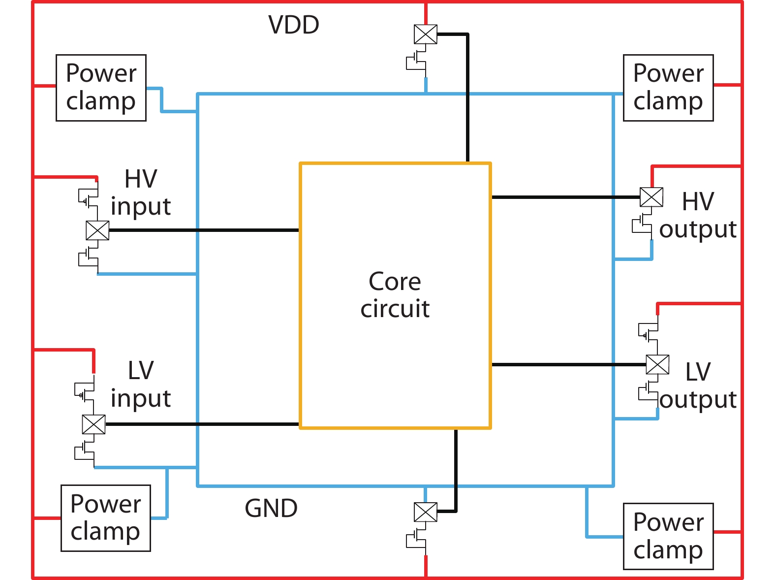
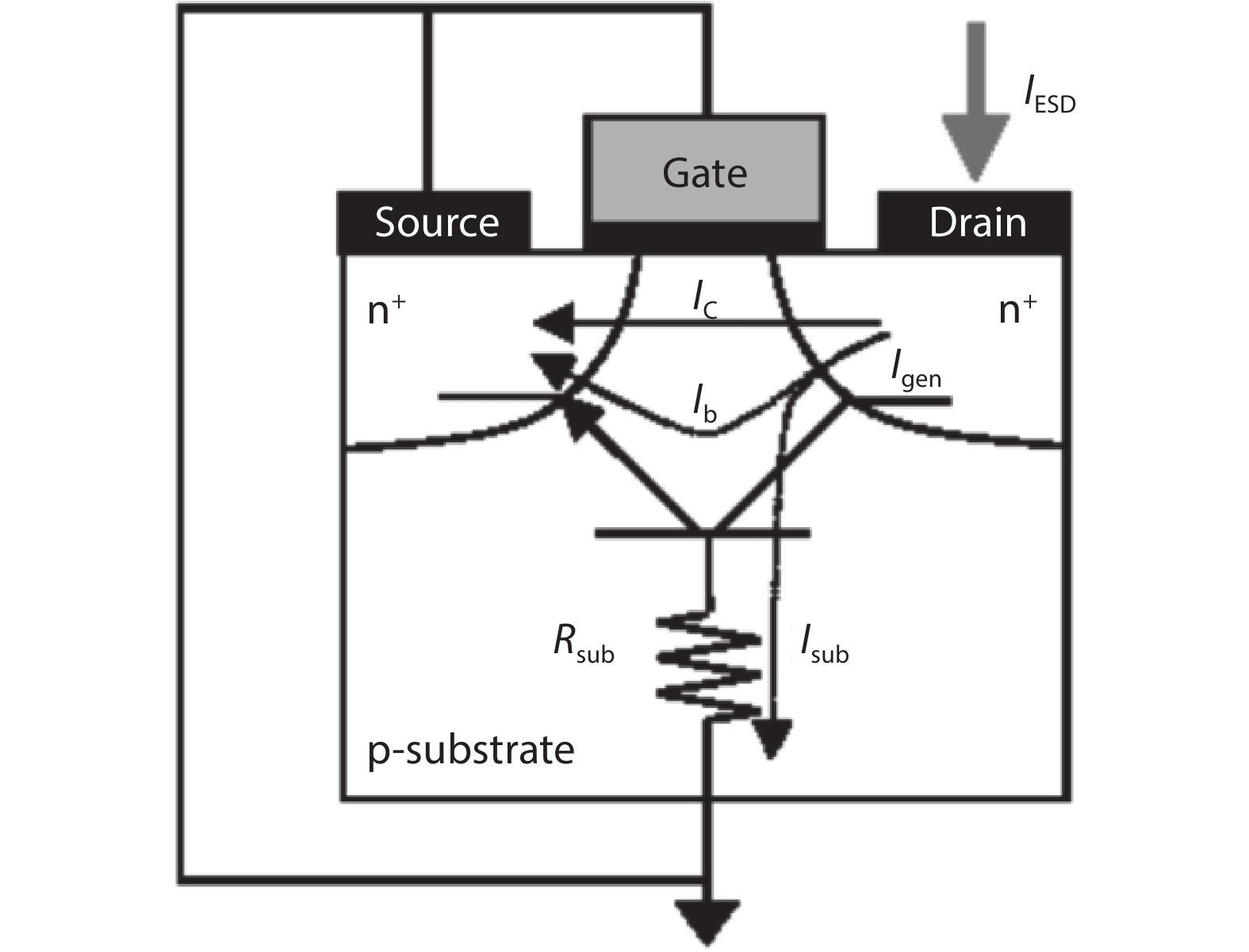
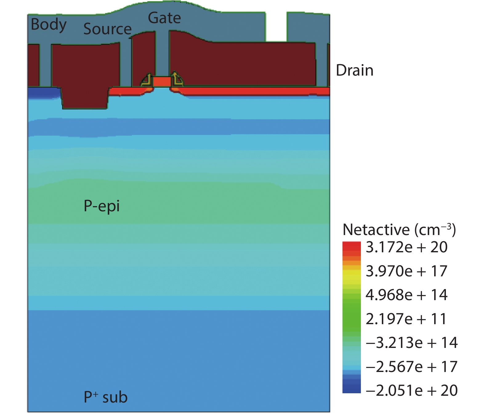
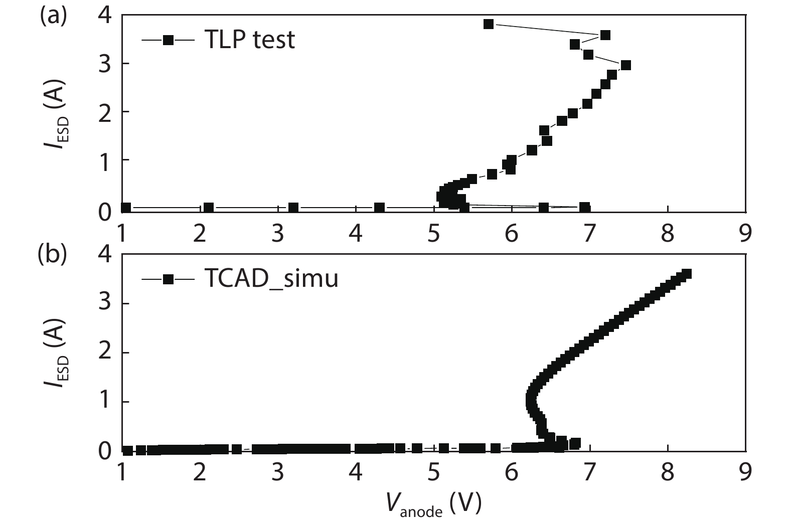
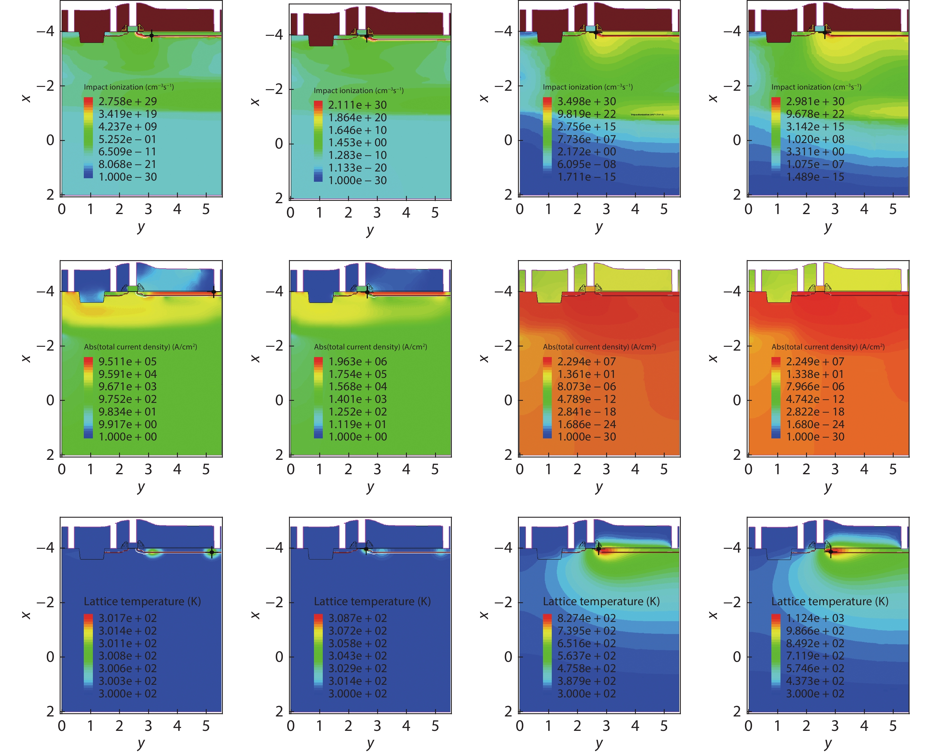
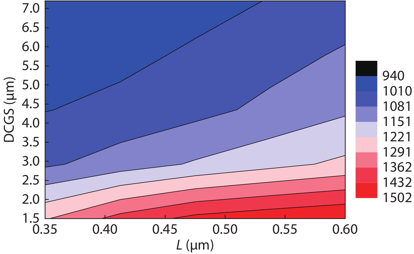
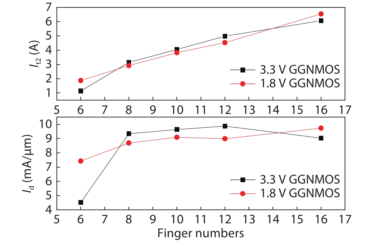
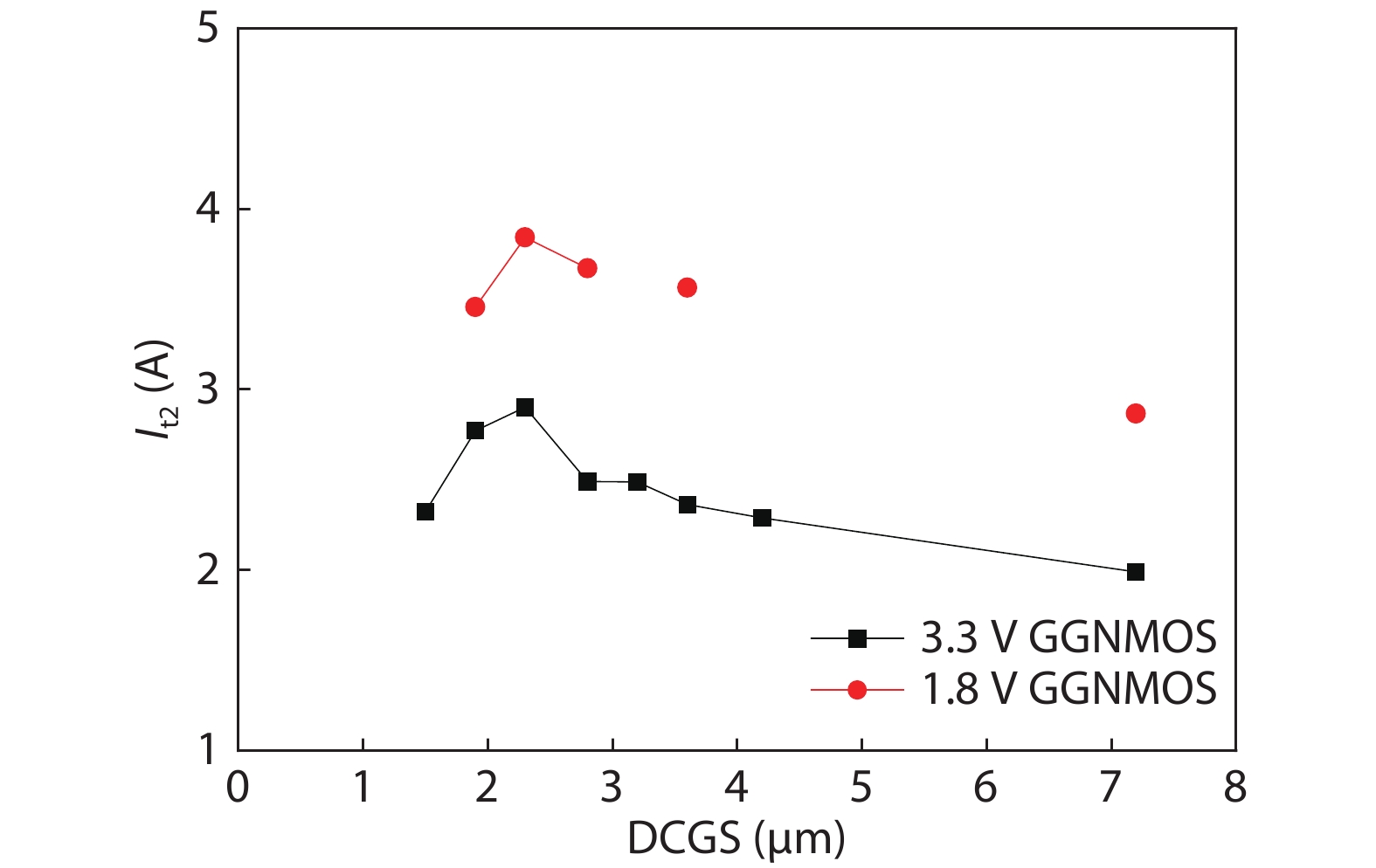
In this paper, the ESD discharge capability of GGNMOS (gate grounded NMOS) device in the radiation-hardened 0.18 μm bulk silicon CMOS process (Rad-Hard by Process: RHBP) is optimized by layout and ion implantation design. The effects of gate length, DCGS and ESD ion implantation of GGNMOS on discharge current density and lattice temperature are studied by TCAD and device simulation. The size of DCGS, multi finger number and single finger width of ESD verification structures are designed, and the discharge capacity and efficiency of GGNMOS devices in ESD are characterized by TLP test technology. Finally, the optimized GGNMOS is verified on the DSP circuit, and its ESD performance is over 3500 V in HBM mode.


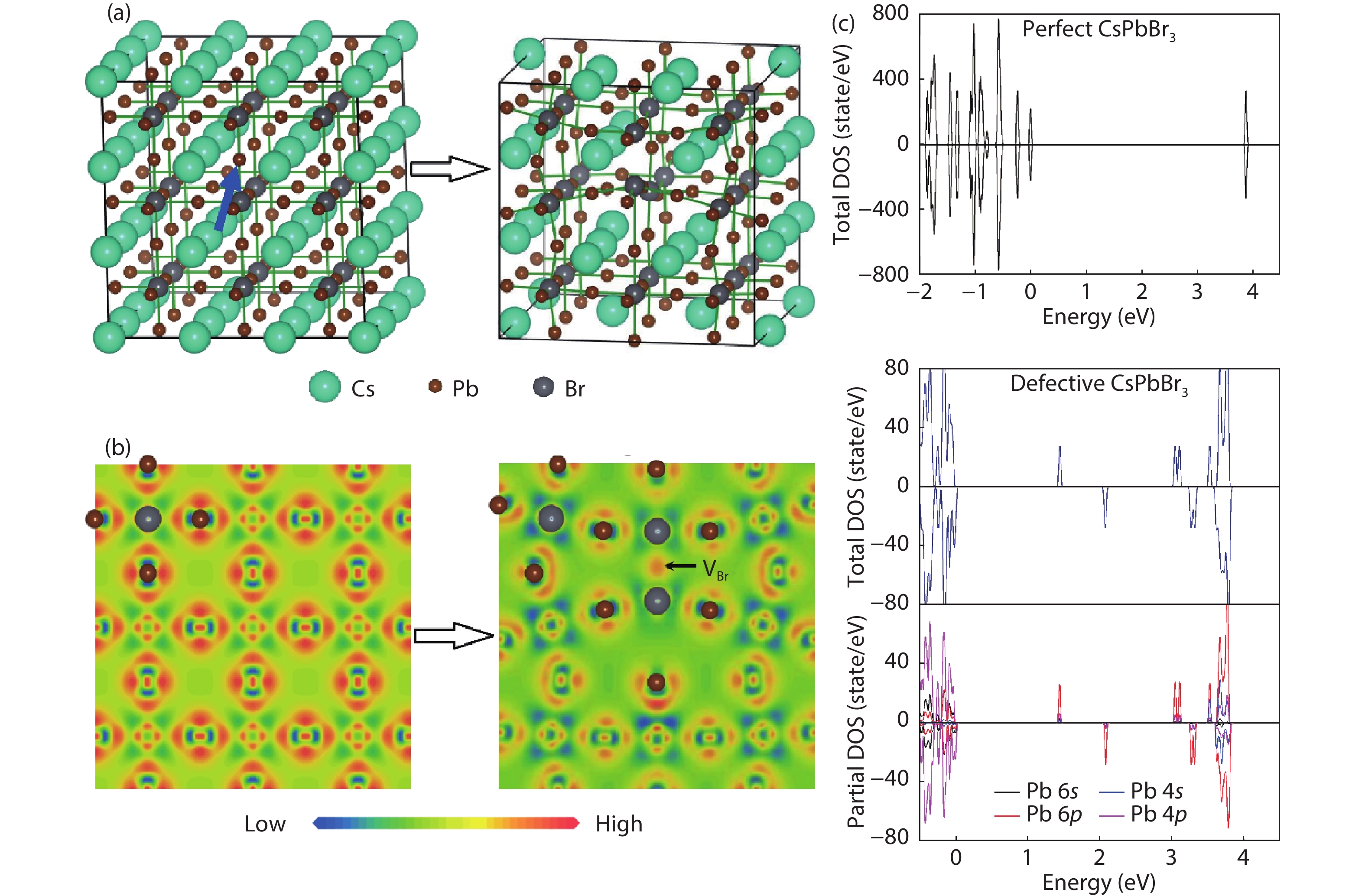
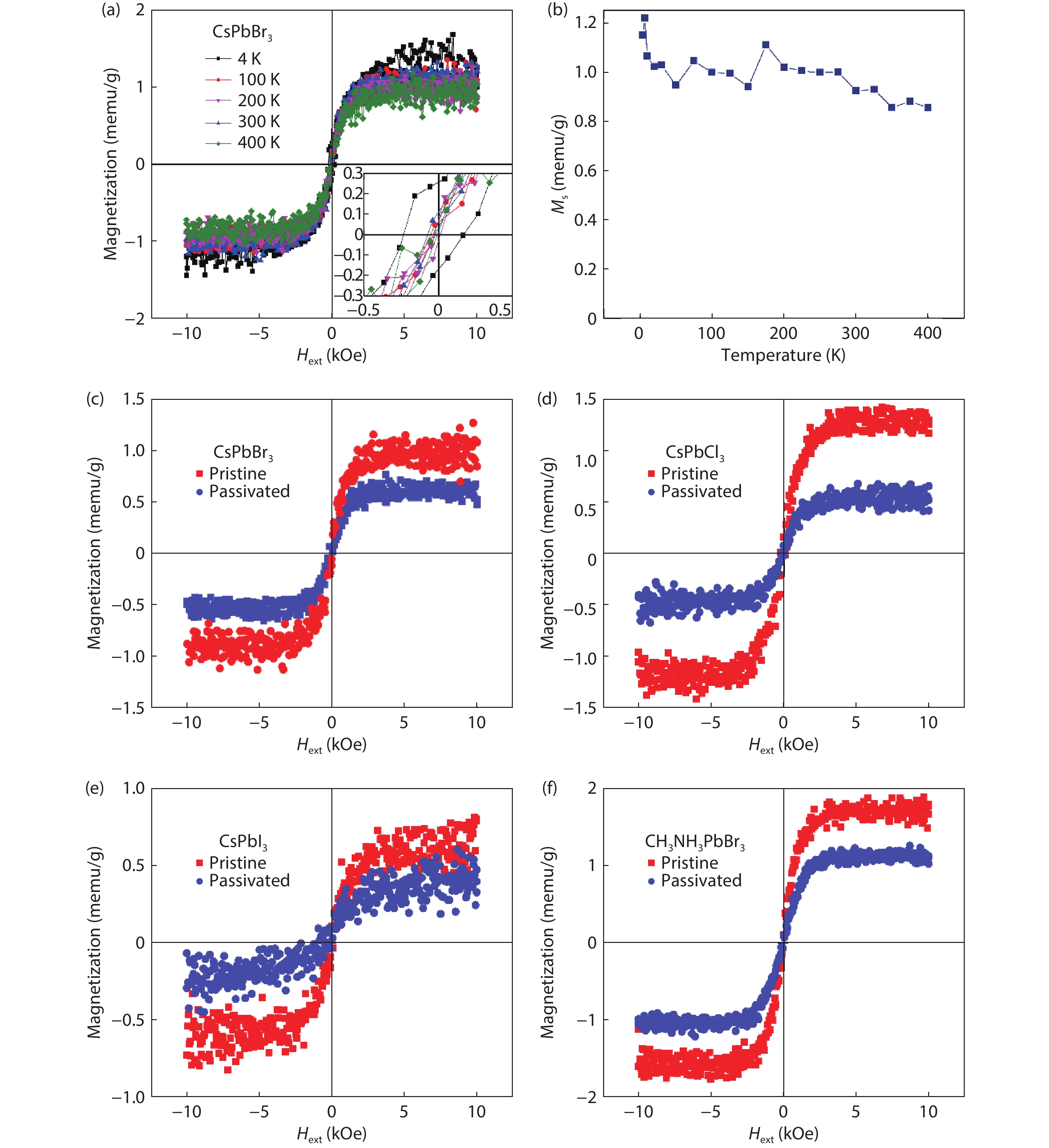
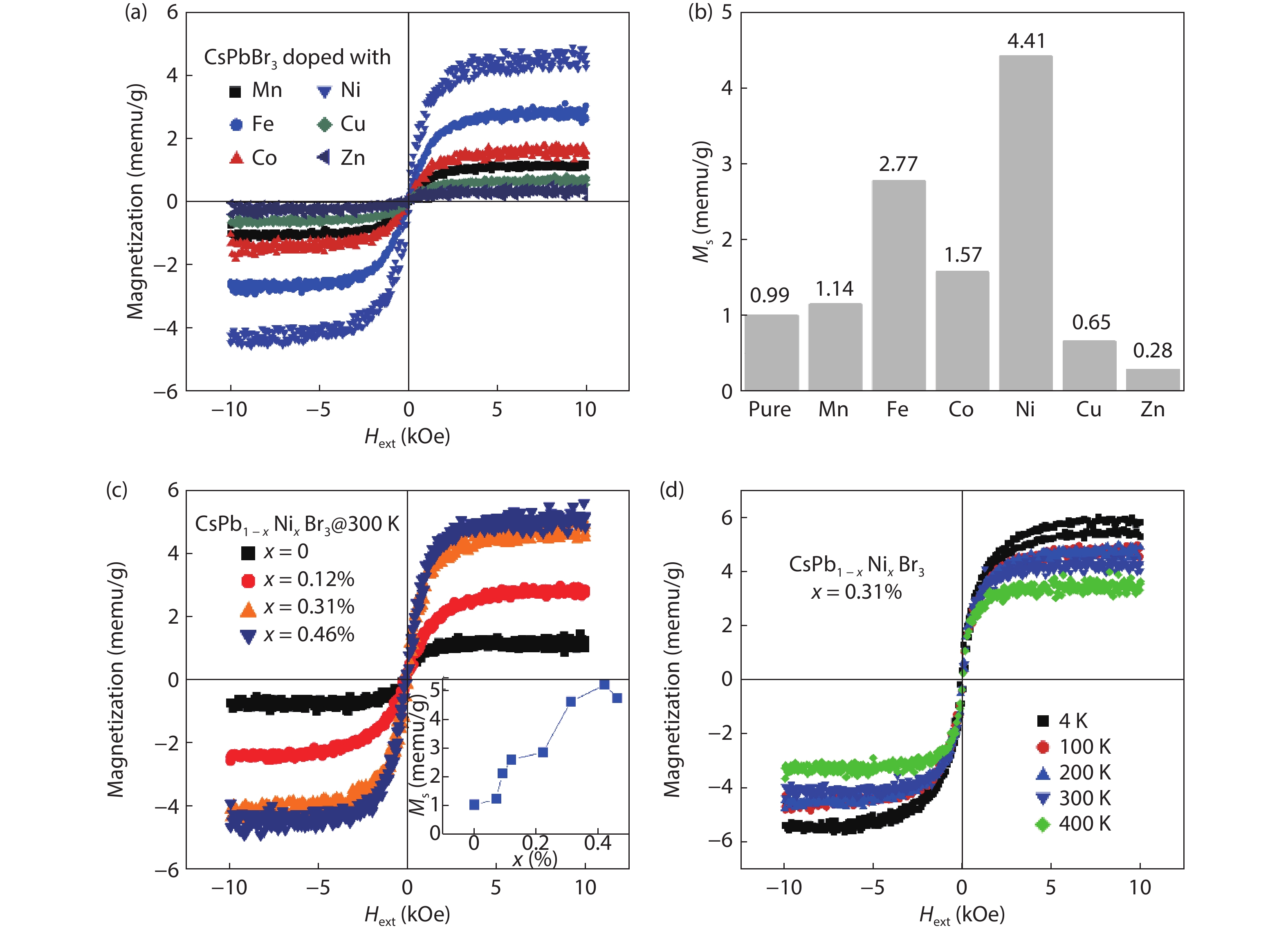
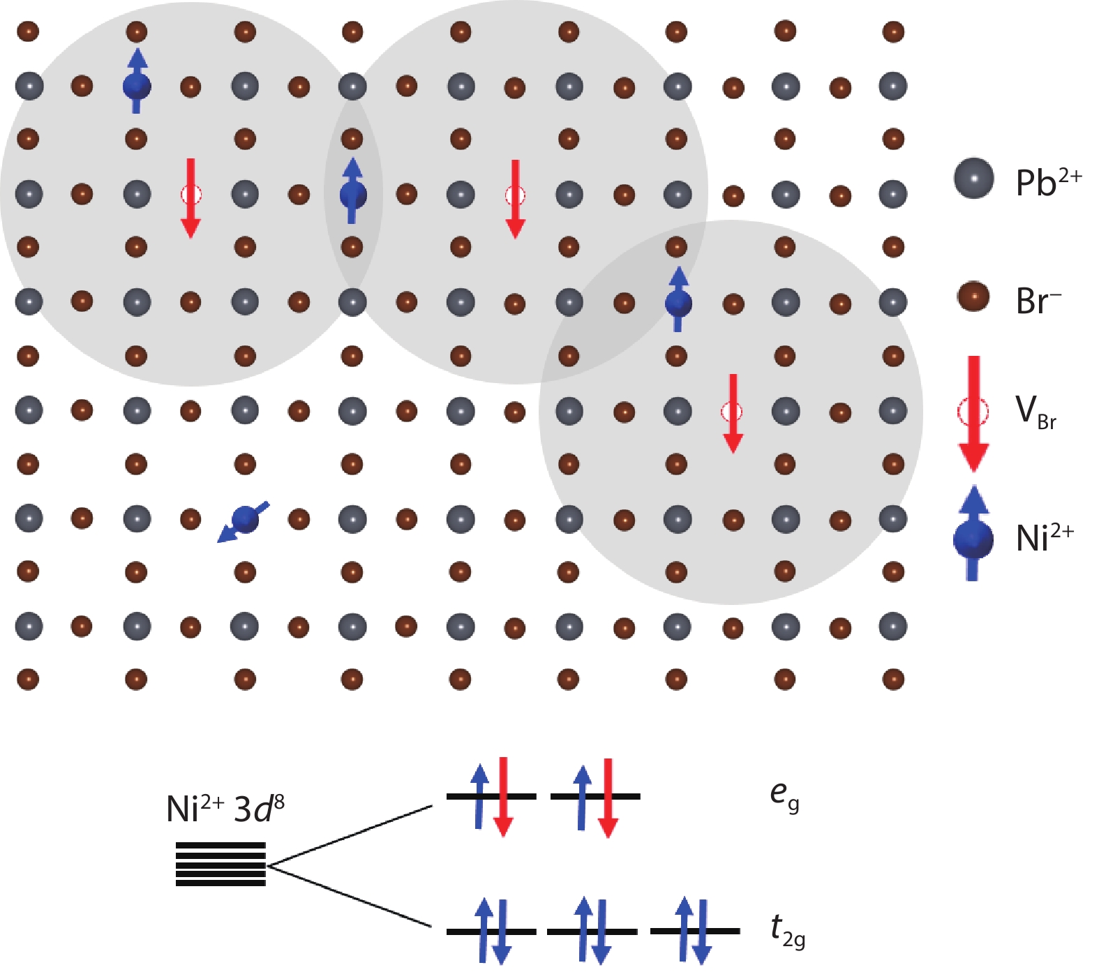
The possibility to induce a macroscopic magnetic moment in lead halide perovskites (LHPs), combined with their excellent optoelectronic properties, is of fundamental interest and has promising spintronic applications. However, these possibilities remain an open question in both theory and experiment. Here, theoretical and experimental studies are performed to explore ferromagnetic states in LHPs originated from lattice defects. First-principle calculations reveal that shallow-level Br vacancies in defective CsPbBr3 can produce spin-splitting states and the coupling between them leads to a ferromagnetic ground state. Experimentally, ferromagnetism at 300 K is observed in room-temperature synthesized CsPbBr3 nanocrystals, but is not observed in hot-injection prepared CsPbBr3 quantum dots and in CsPbBr3 single crystals, highlighting the significance played by vacancy defects. Furthermore, the ferromagnetism in the CsPbBr3 nanocrystals can be enhanced fourfold with Ni2+ ion dopants, due to enhancement of the exchange coupling between magnetic polarons. Room-temperature ferromagnetism is also observed in other LHPs, which suggests that vacancy-induced ferromagnetism may be a universal feature of solution-processed LHPs, which is useful for future spintronic devices.

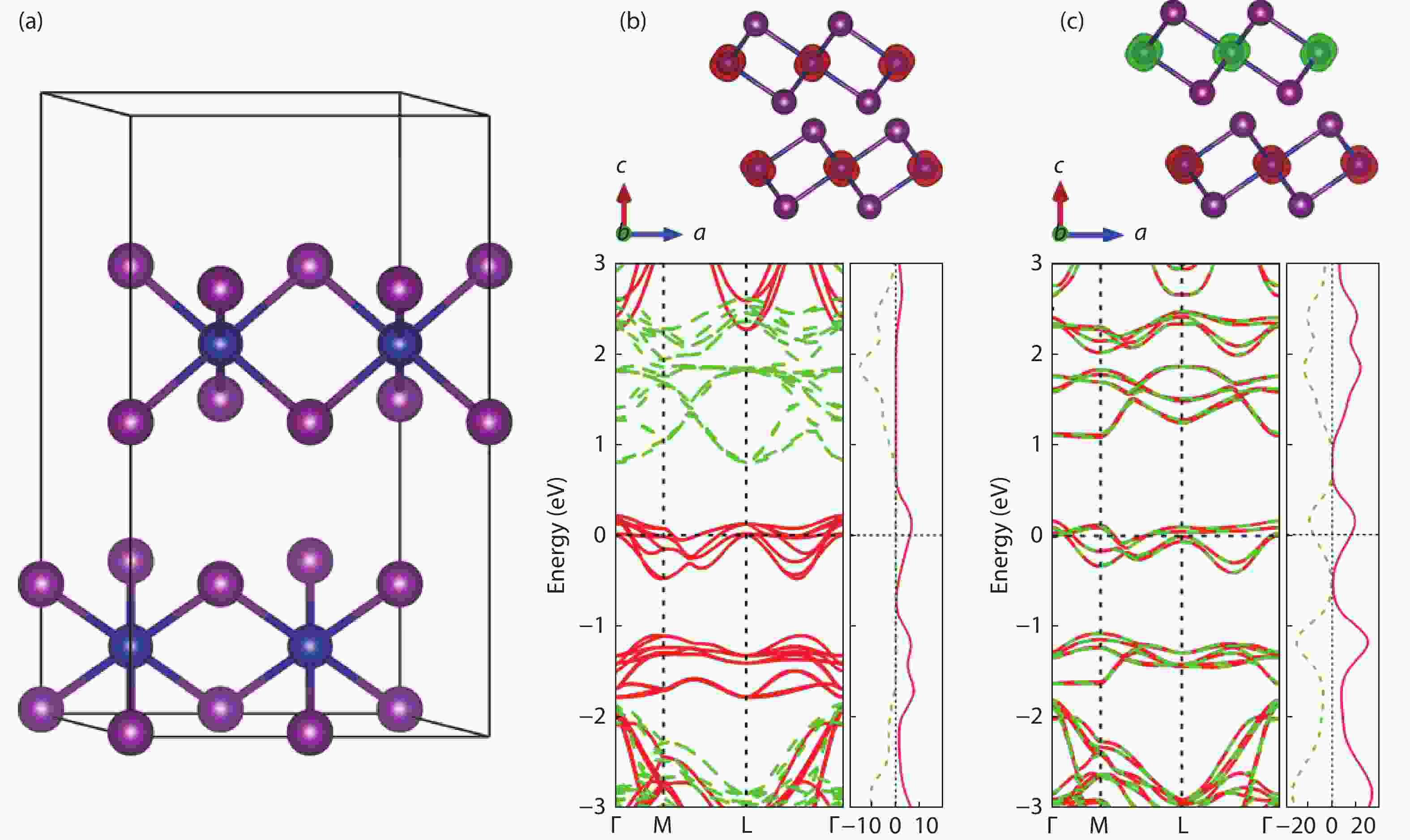
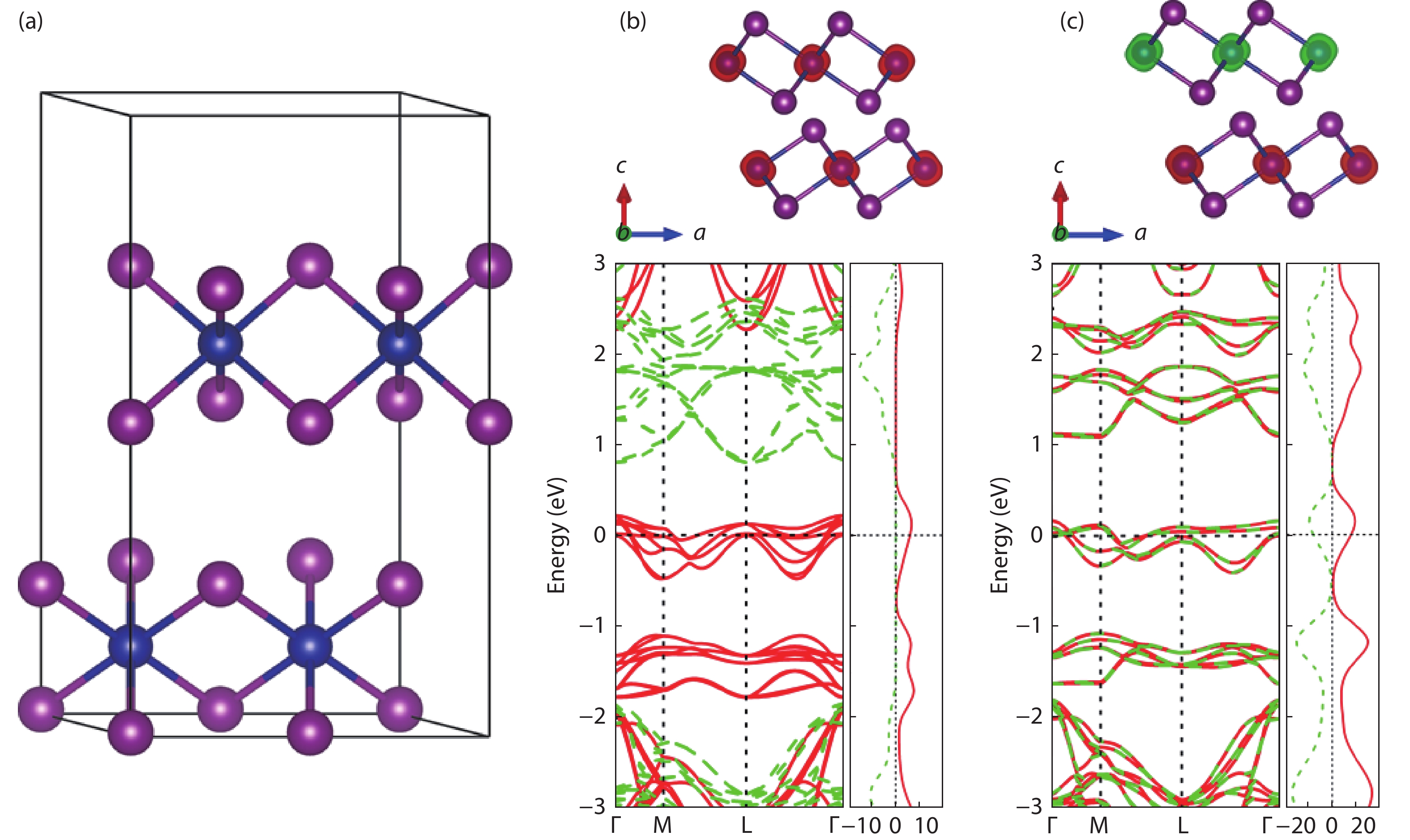
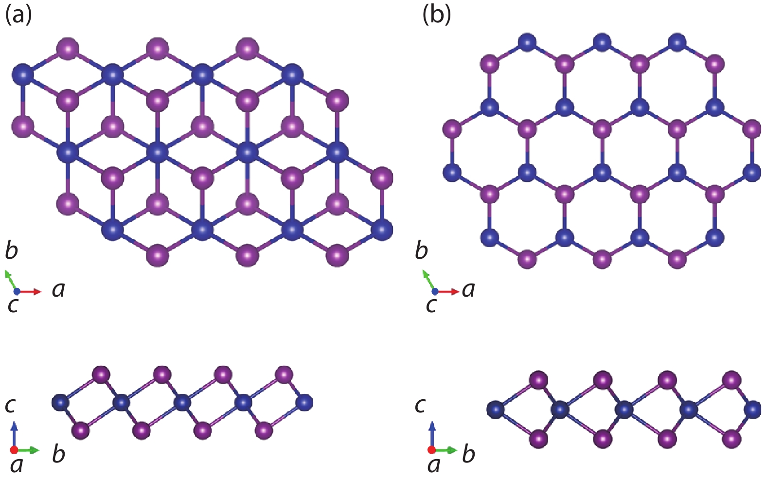
The two-dimensional (2D) ferromagnetic materials and the related van der Waals homostructures have attracted considerable interest, while the 2D antiferromagnetic material has not yet been reported. Based on first-principles calculations, we investigate both electronic structures and magnetic orderings of bulk and monolayer of chromium diiodides (CrI2). We demonstrate a counter-intuitive fact that the ground state of the free-standing monolayer of CrI2 is antiferromagnetic though the bulk possesses macroscopic ferromagnetic ordering. The interlayer interaction remains antiferromagnetic up to few-layer scenarios. The unique feature of CrI2 makes it an ideal workbench to investigate the relation between magnetic couplings and interlayer van der Waals interactions, and may offer an opportunity to 2D antiferromagnetic spintronic devices.
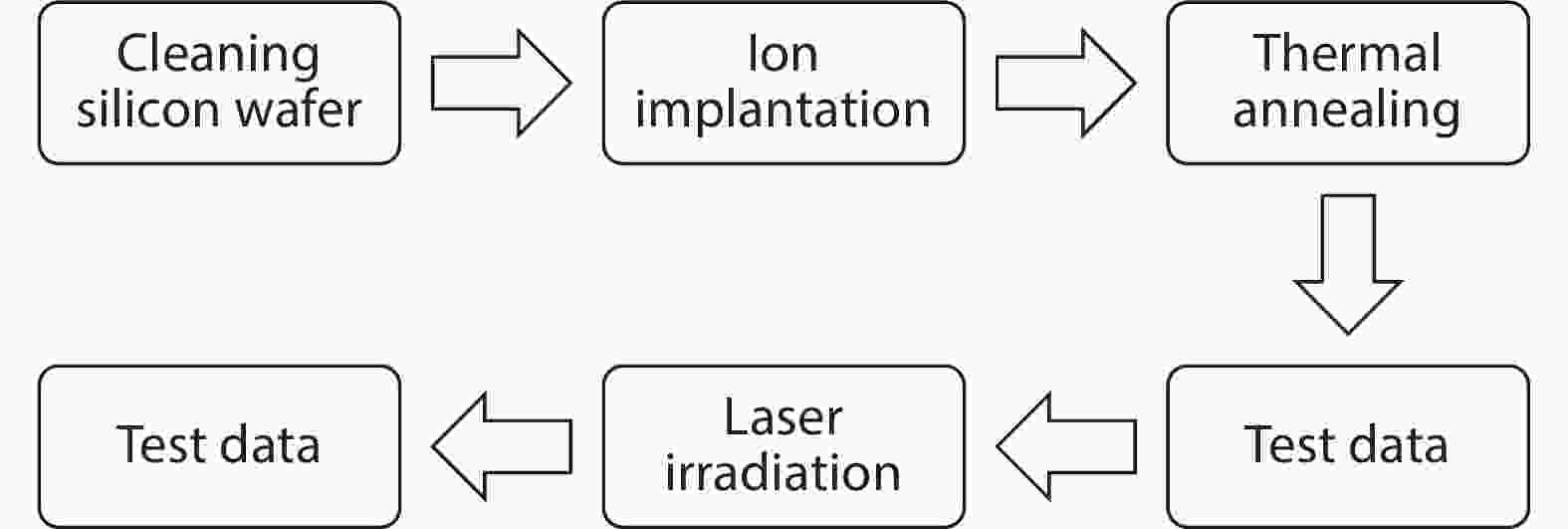
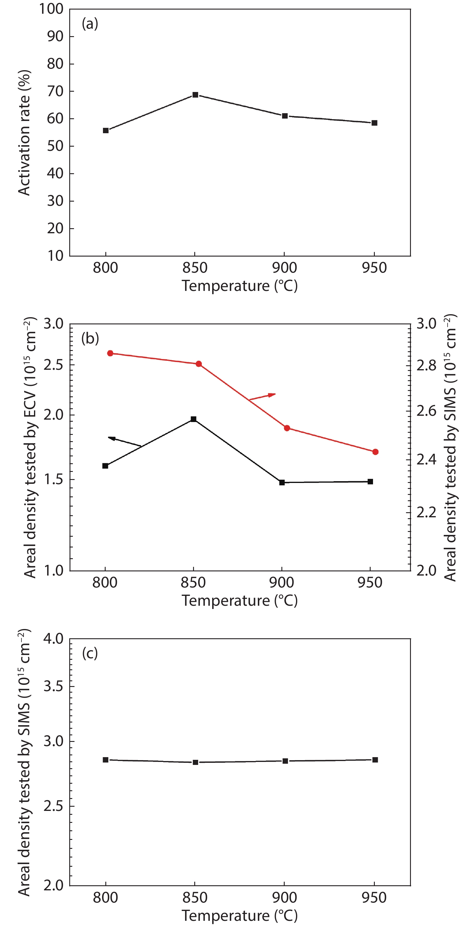
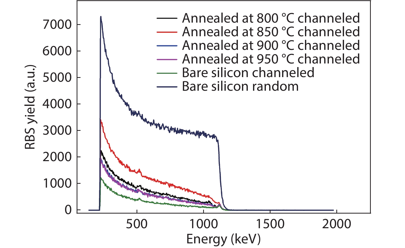
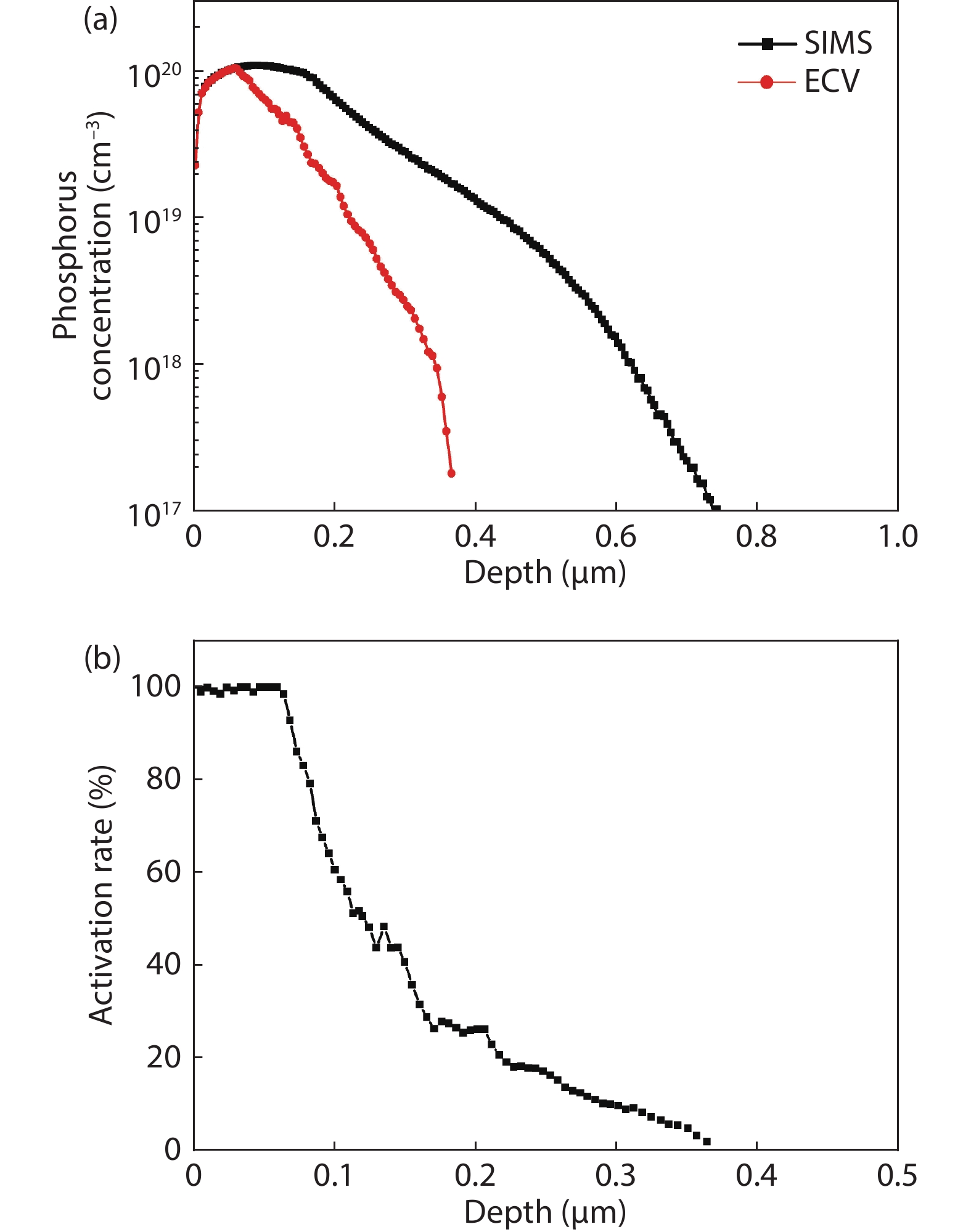
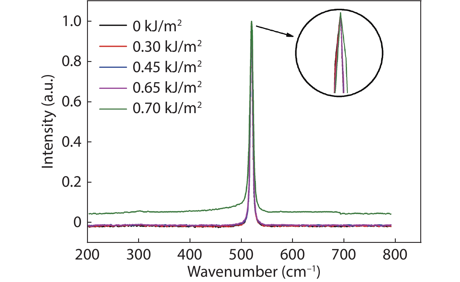
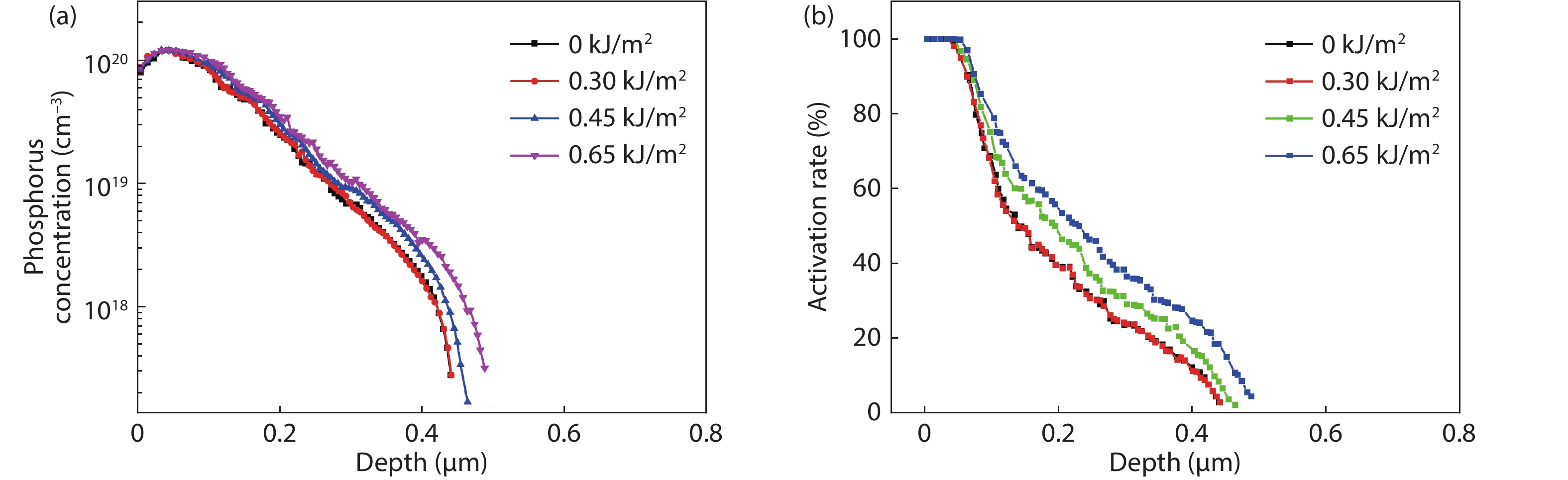
Thermal annealing and laser irradiation were used to study the activation rate of phosphorus in silicon after ion implantation. The activation rate refers to the ratio of activated impurity number to the total impurity number in the sample. After injecting phosphorus with the dose and energy (energy = 55 keV, dose = 3 × 1015 cm–2), the samples were annealed at different temperatures, and laser irradiation experiments were performed after annealing. The experimental results showed that the activation rate of phosphorus was the highest at 850 °C, and the highest activation rate was 67%. Upon femtosecond laser irradiation samples after thermal annealing, while keeping the crystalline silicon surface without damage, the activation rate was improved. When the energy-flux density of the femtosecond laser was 0.65 kJ/cm2, the activation rate was the highest, increasing from 67% to 74.81%.


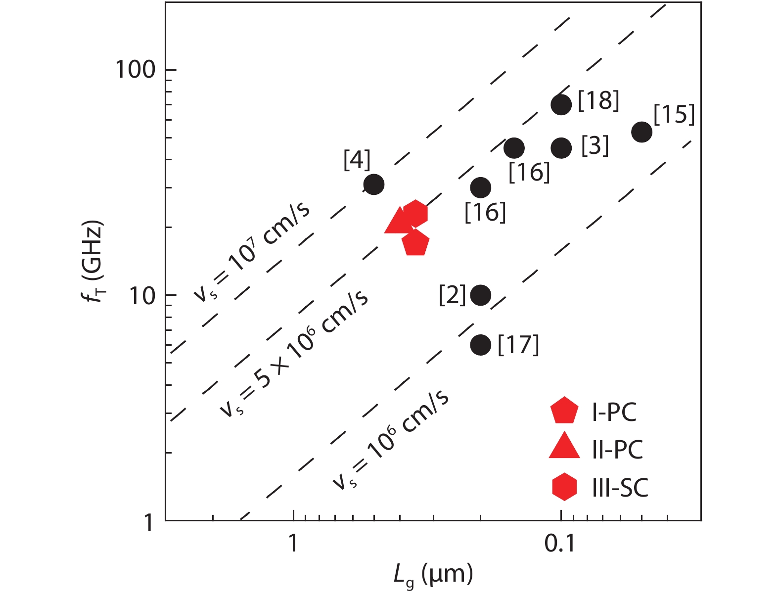
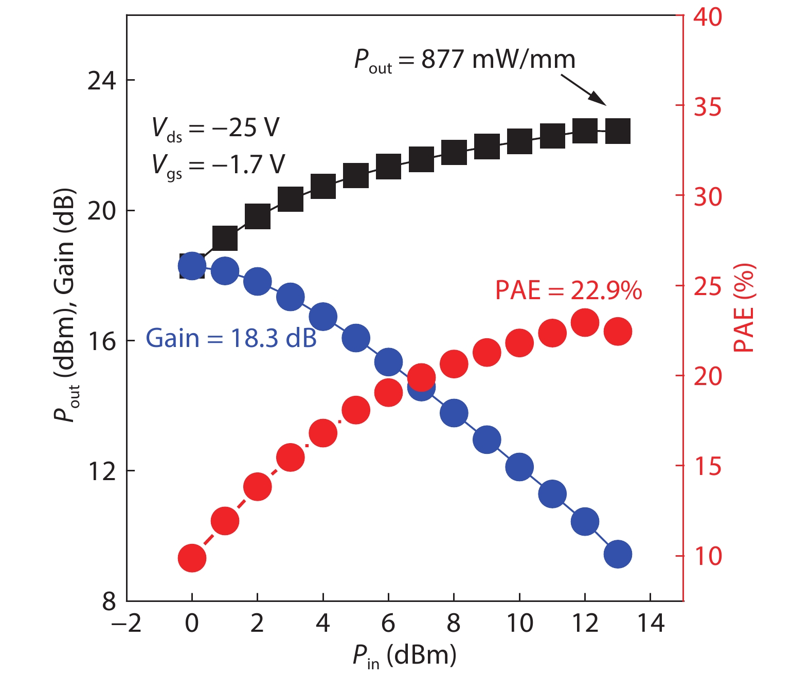
In this work, we investigate the influence of defect concentration of the diamond substrates on the performance of hydrogen-terminated diamond field-effect transistors by Raman spectra, pulsed I–V characteristics analysis, and radio frequency performances measurements. It is found that a sample with higher defect concentration shows larger drain-lag effect and lower large-signal output power density. Defects in the diamond act as traps in the carrier transport and have a considerable influence on the large-signal output power density of diamond field-effect transistors. This work should be helpful for further performance improvement of the microwave power diamond devices.
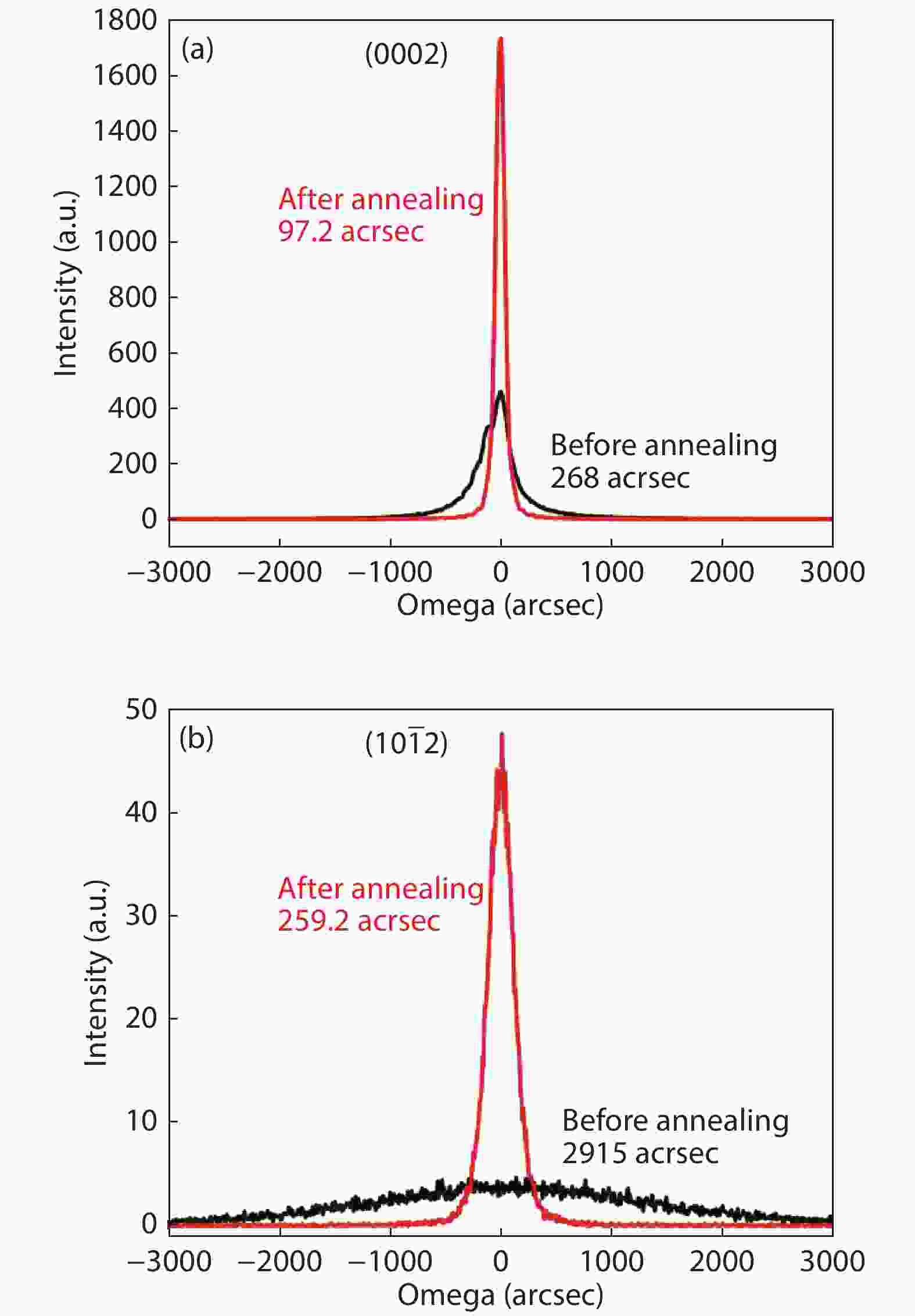
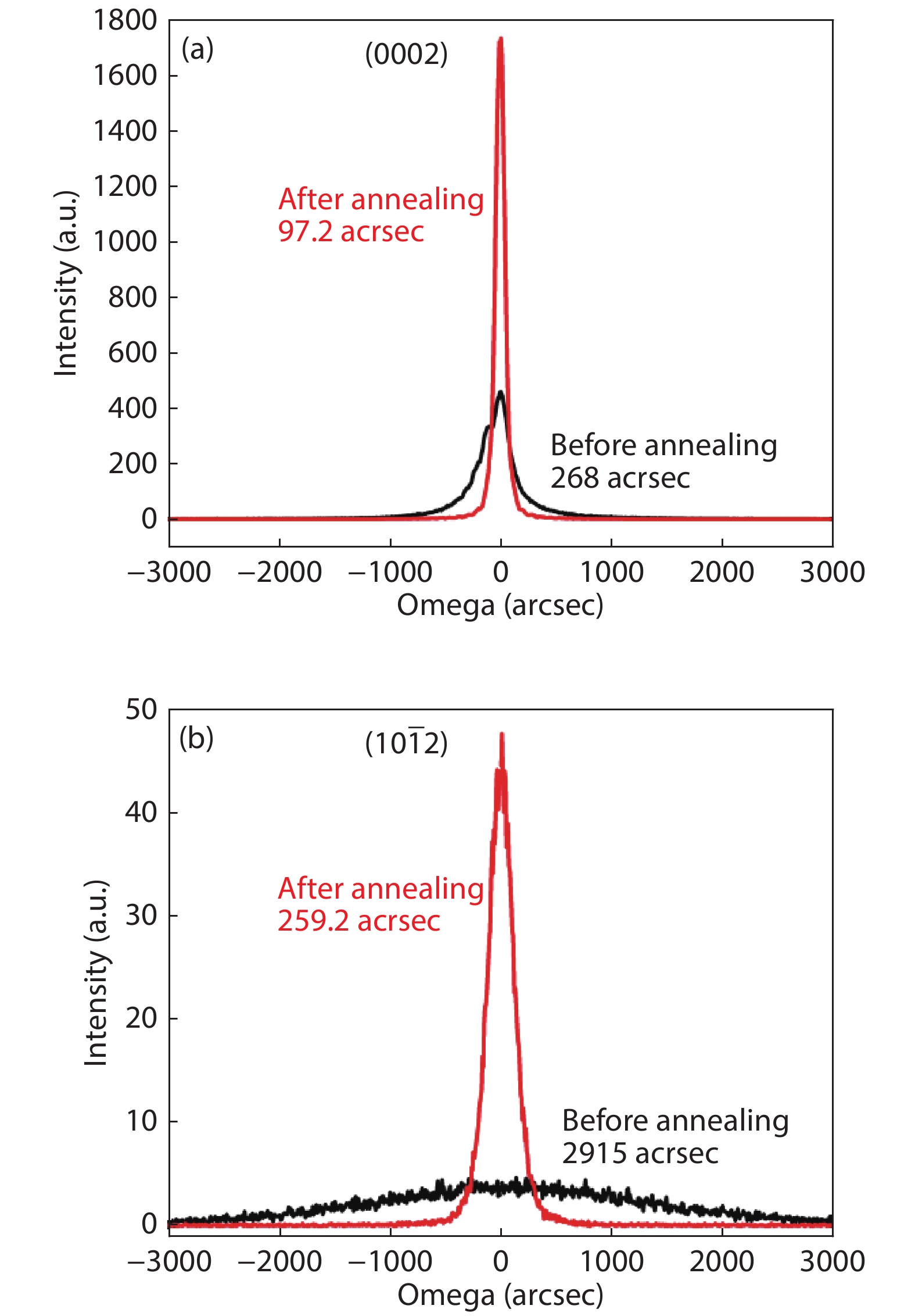
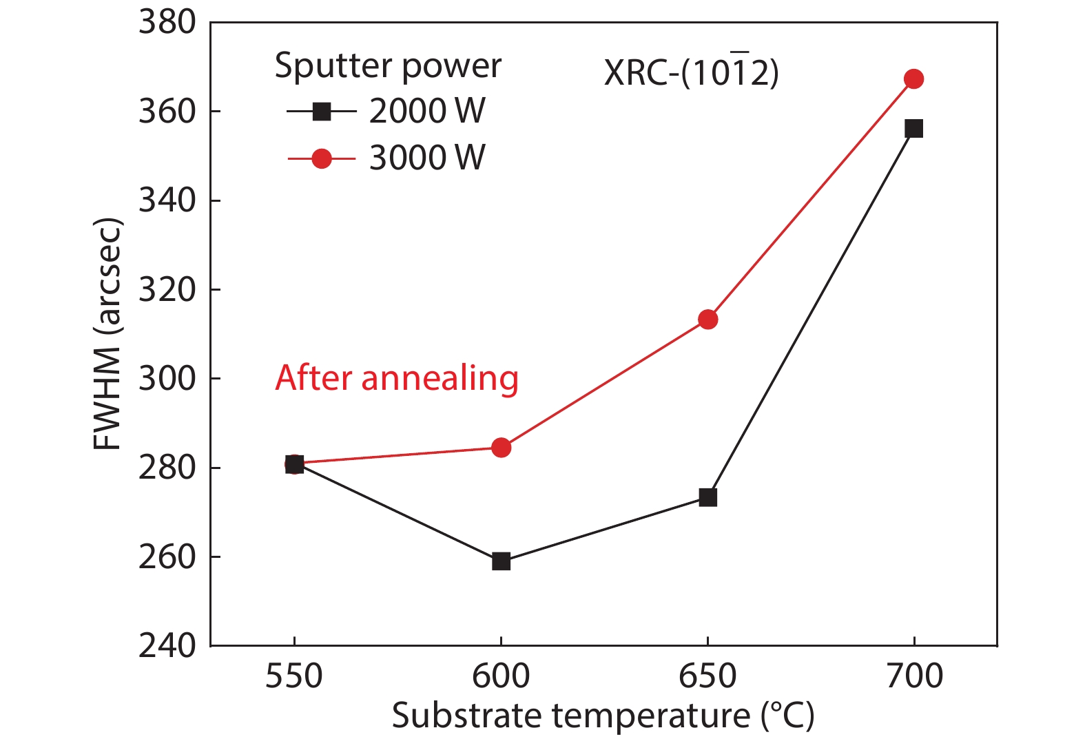
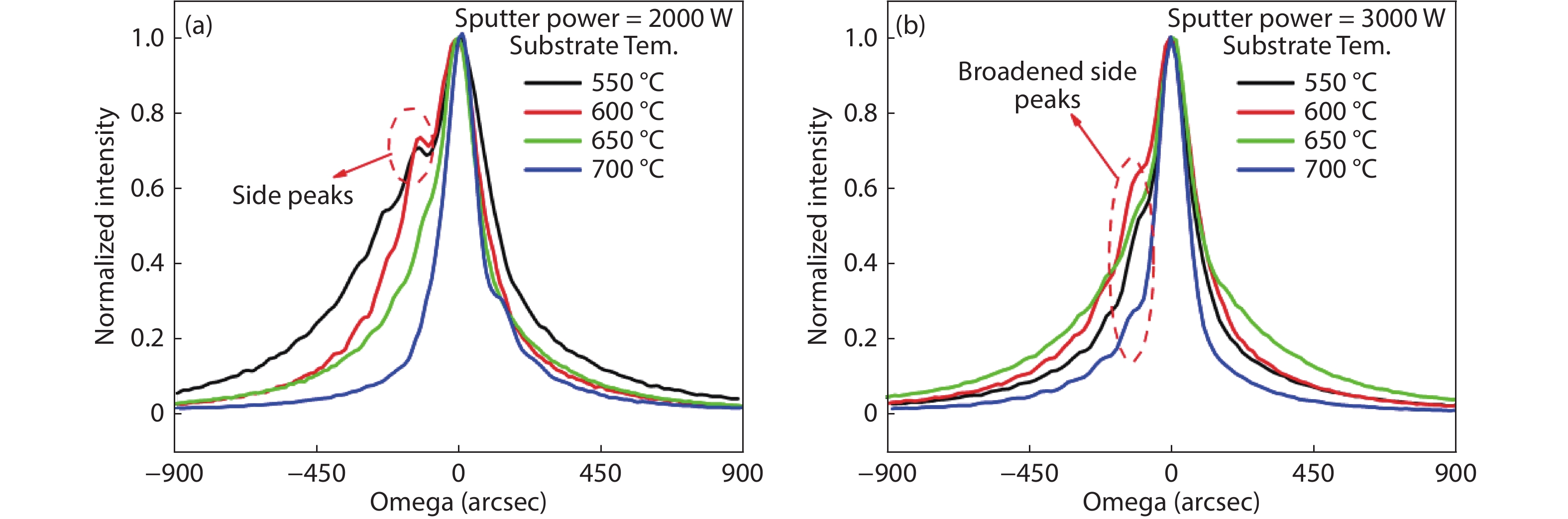
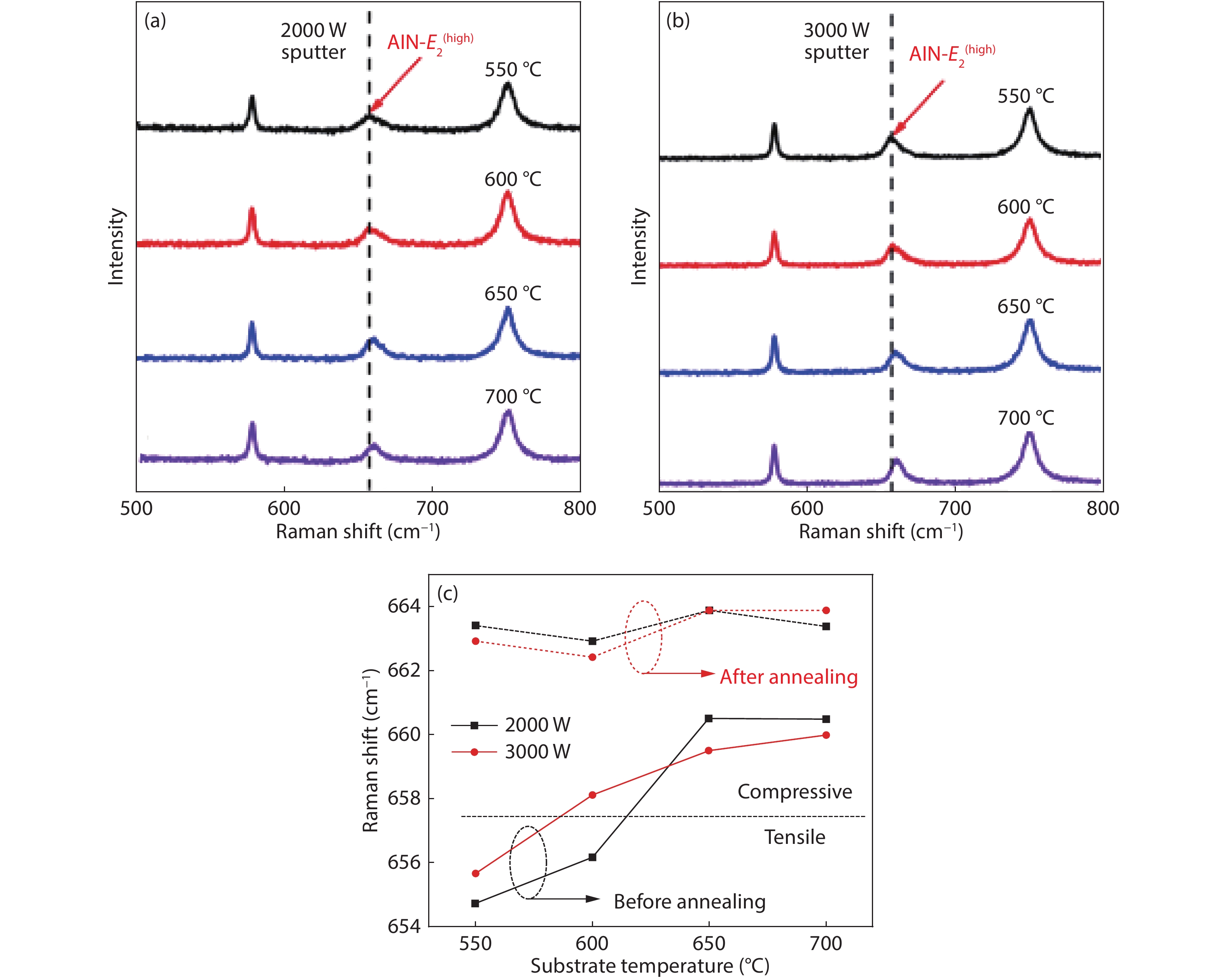
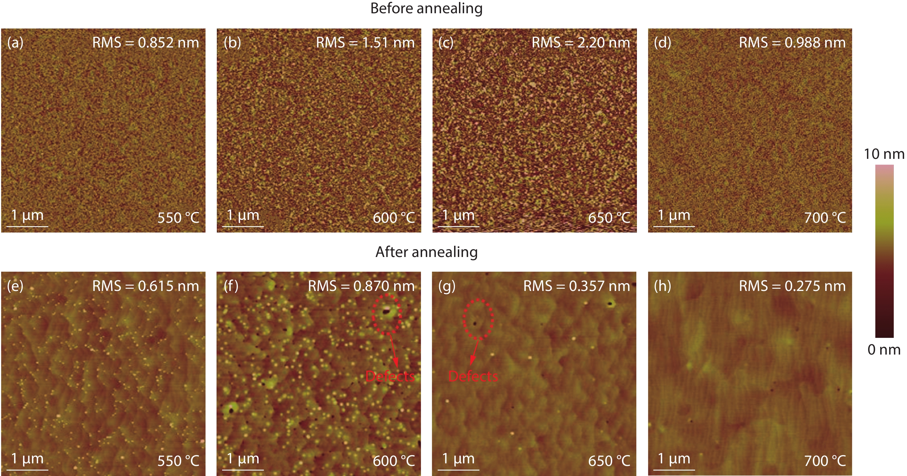
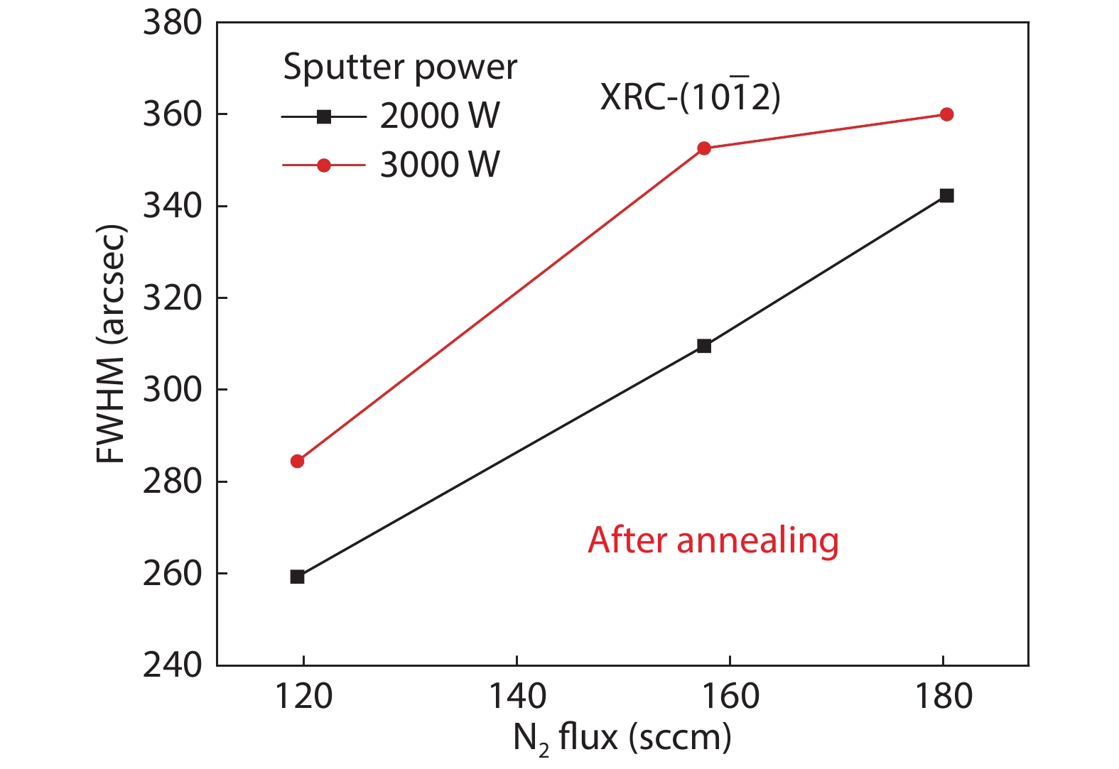
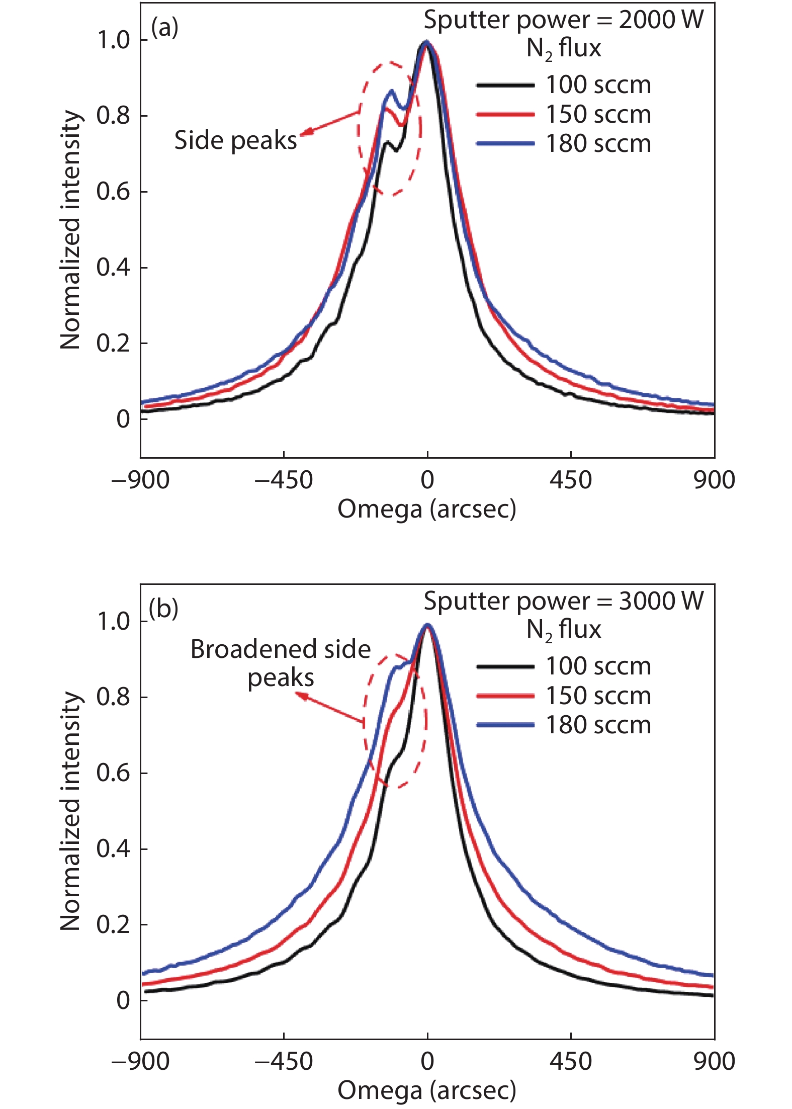
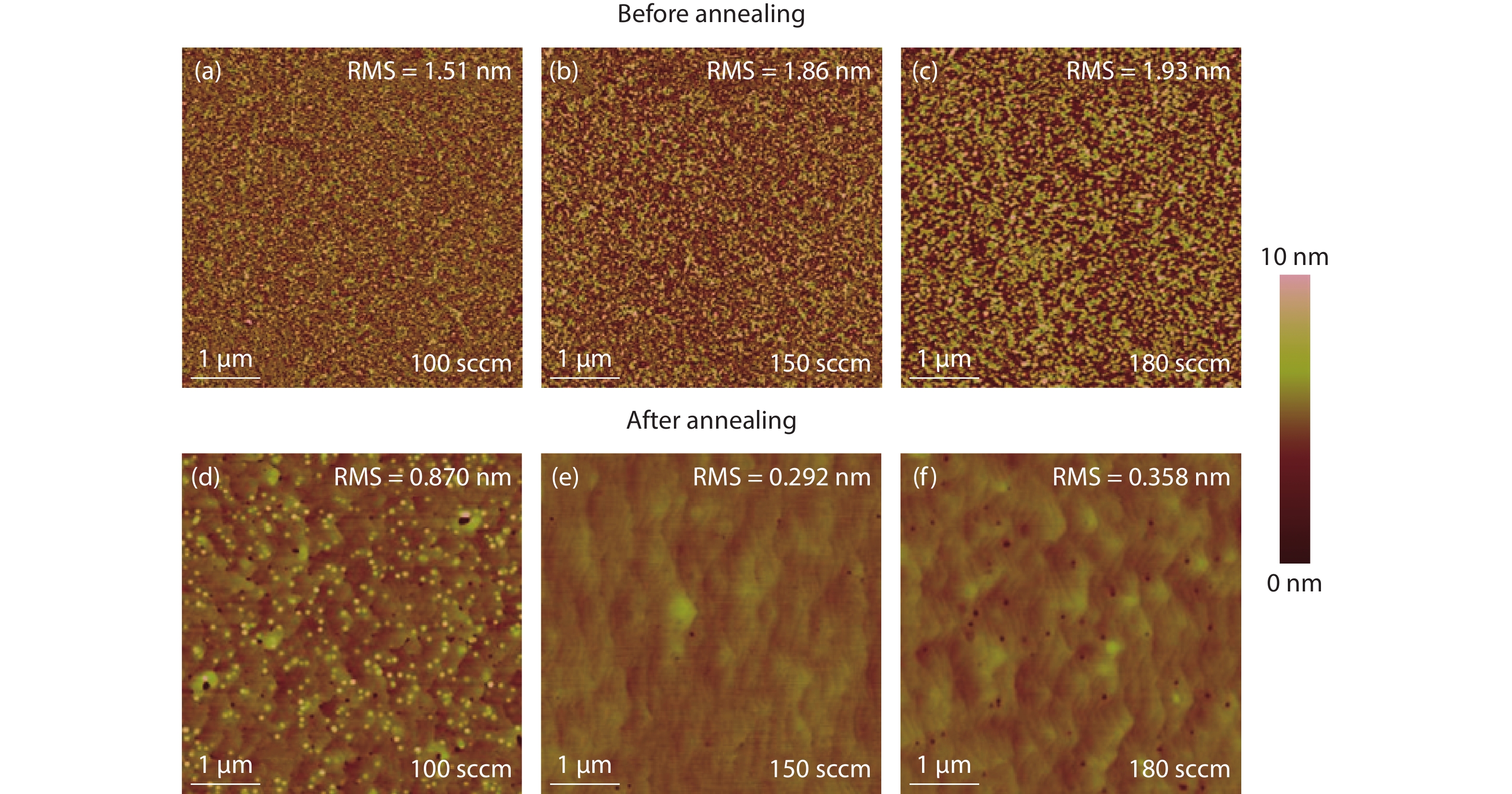
High-quality AlN/sapphire templates were fabricated by the combination of sputtering and high-temperature (HT) annealing. The influence of sputtering parameters including nitrogen flux, radio frequency power, and substrate temperature on the crystalline quality and surface morphology of annealed AlN films were investigated. With lower substrate temperature, lower power, and lower N2 flux, the full width at half maximum of the X-ray rocking curve for AlN (0002) and (10

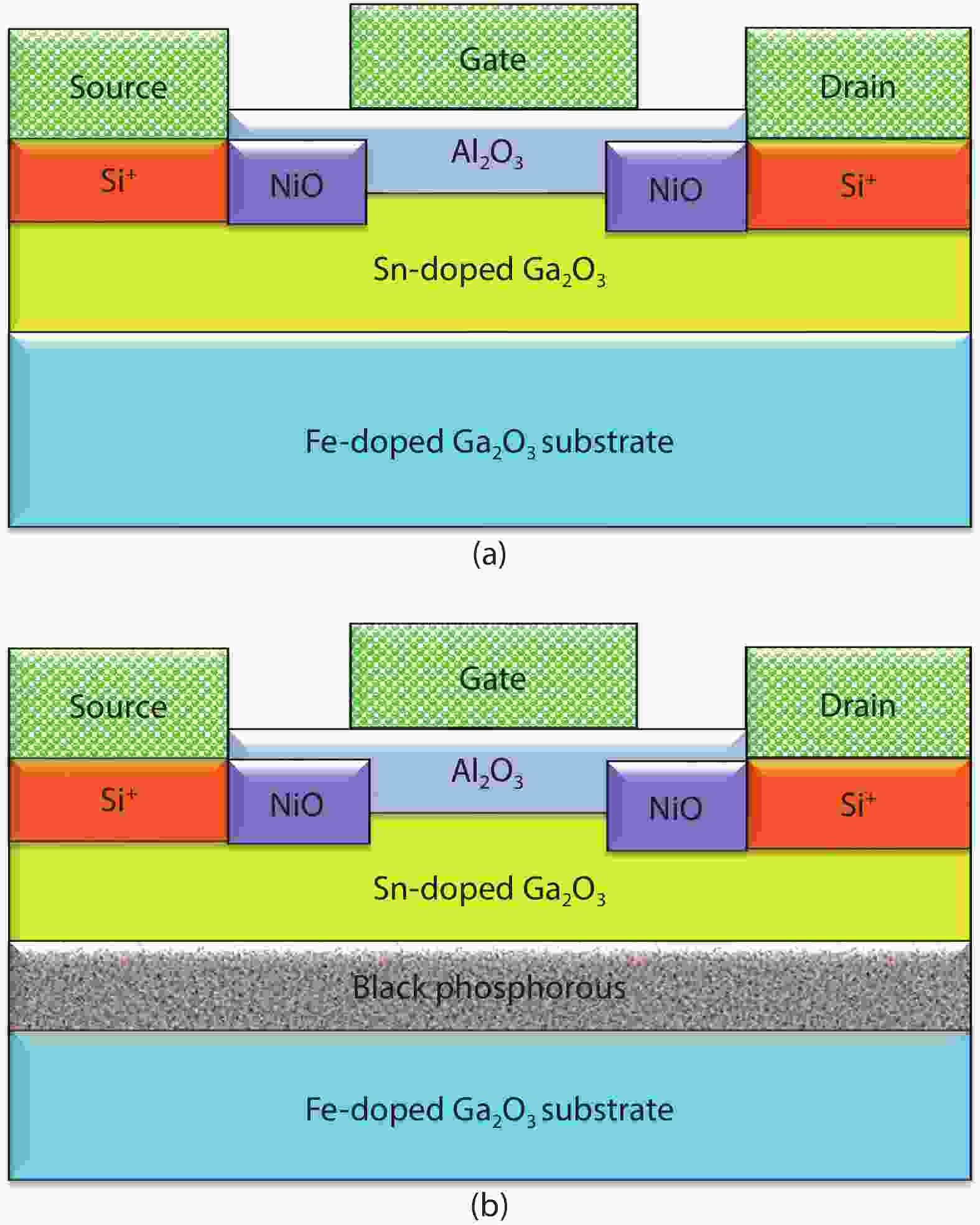
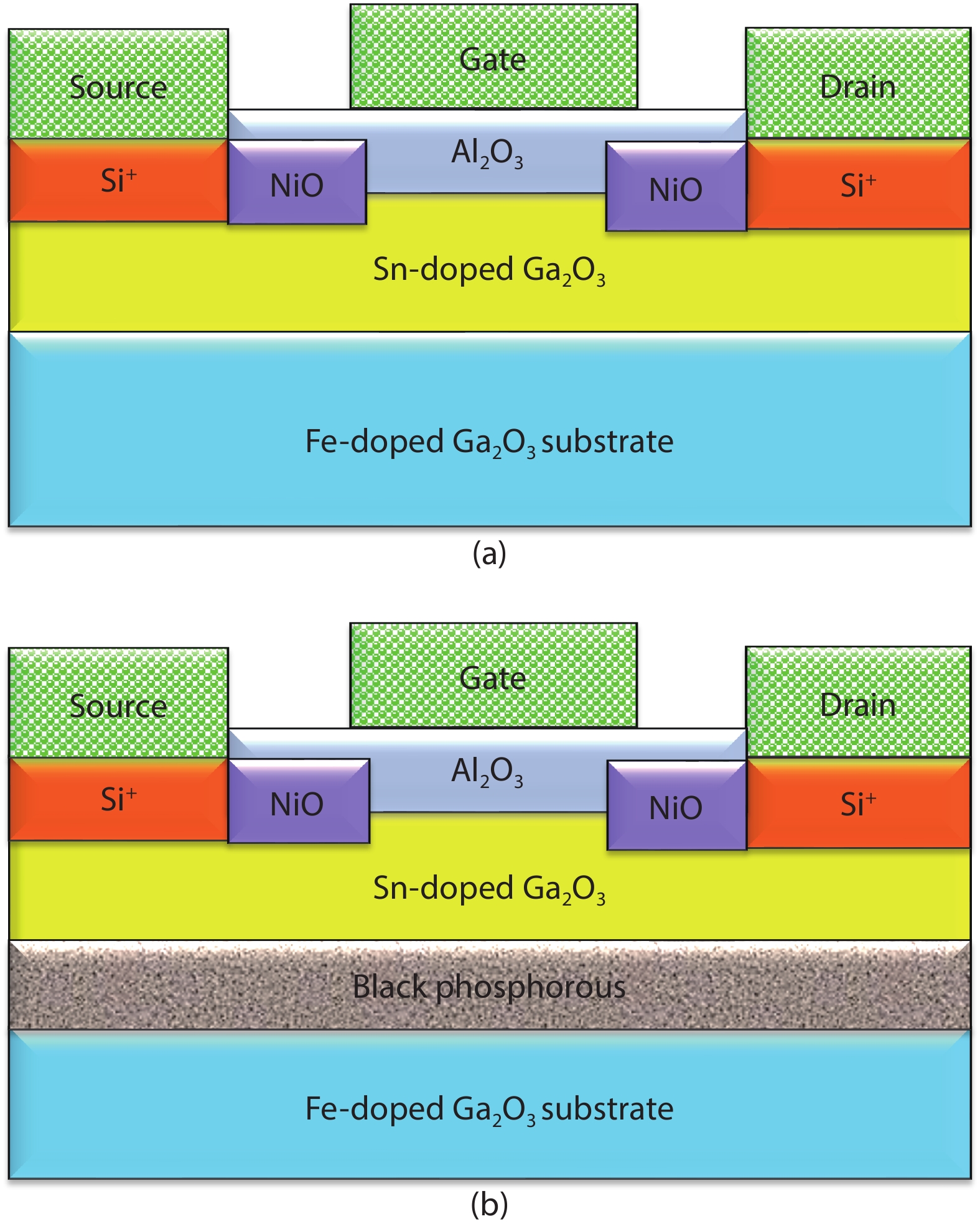
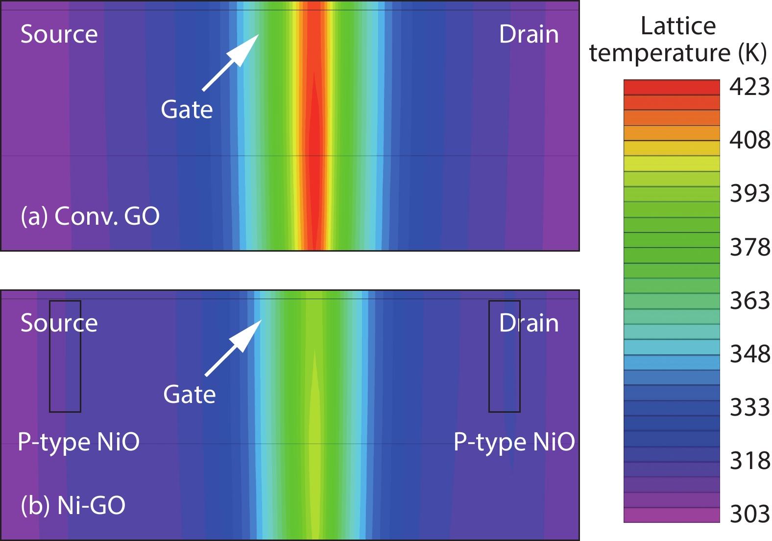
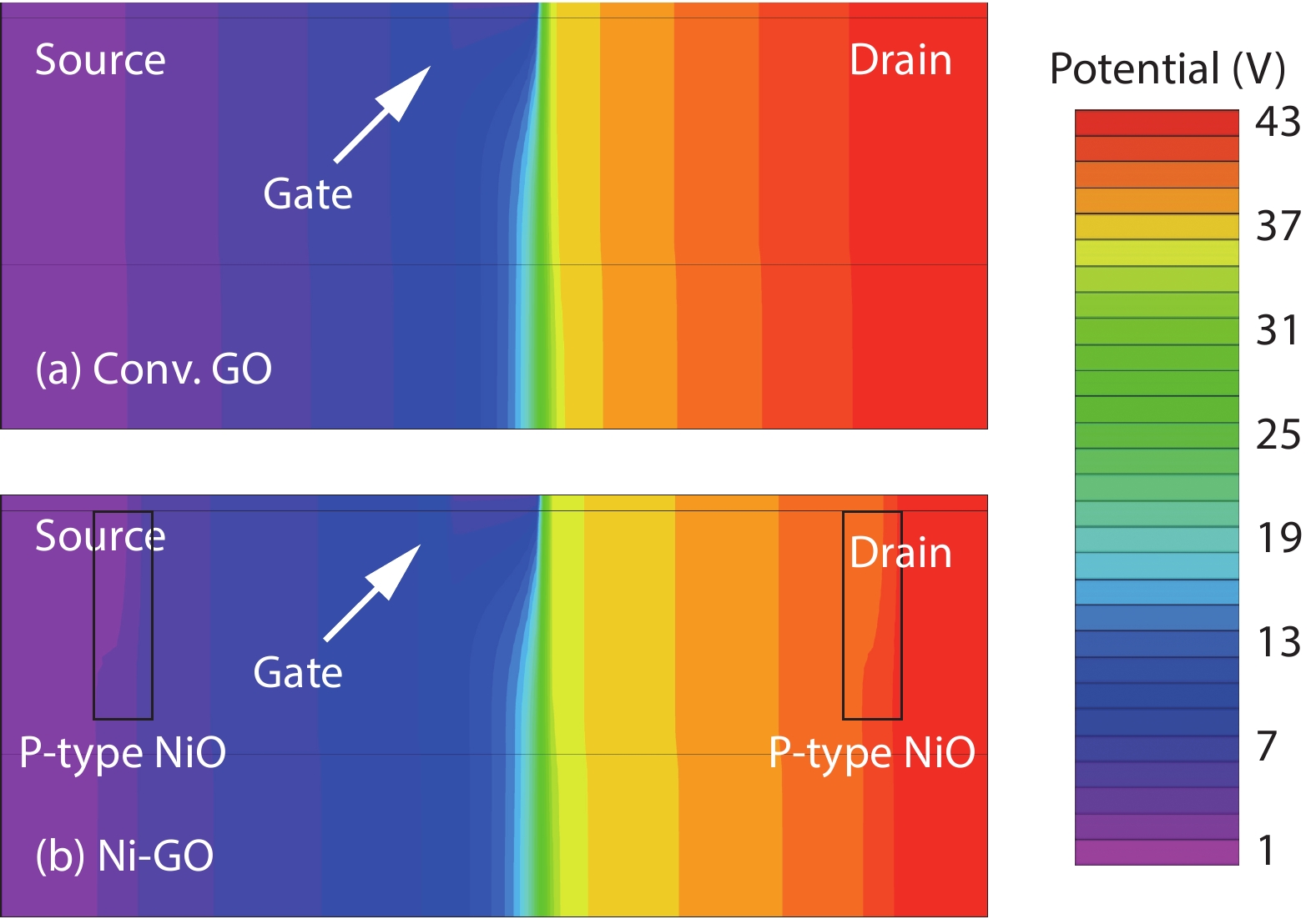
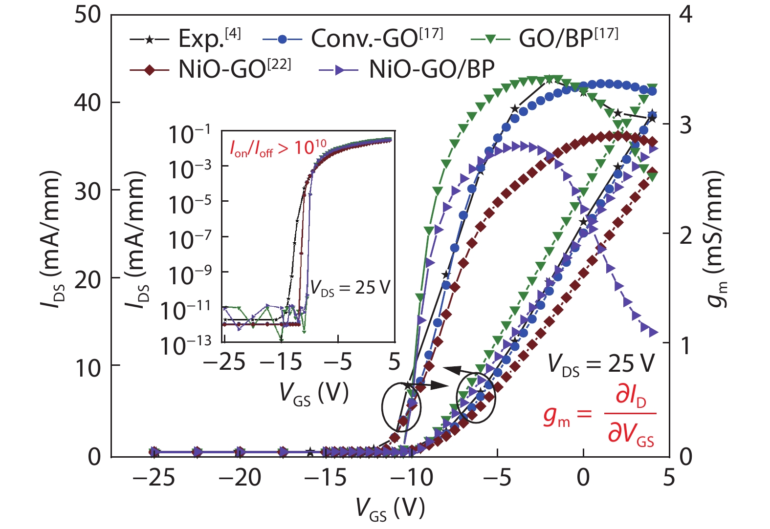
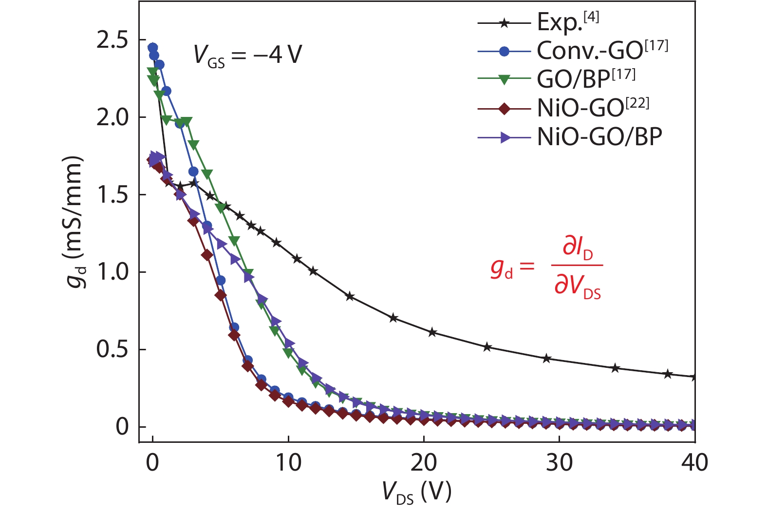
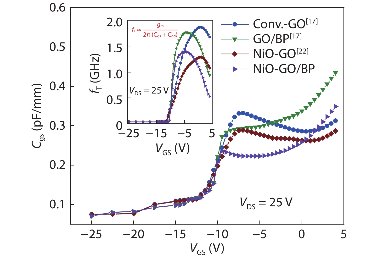
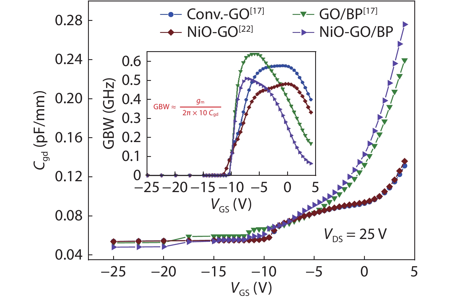
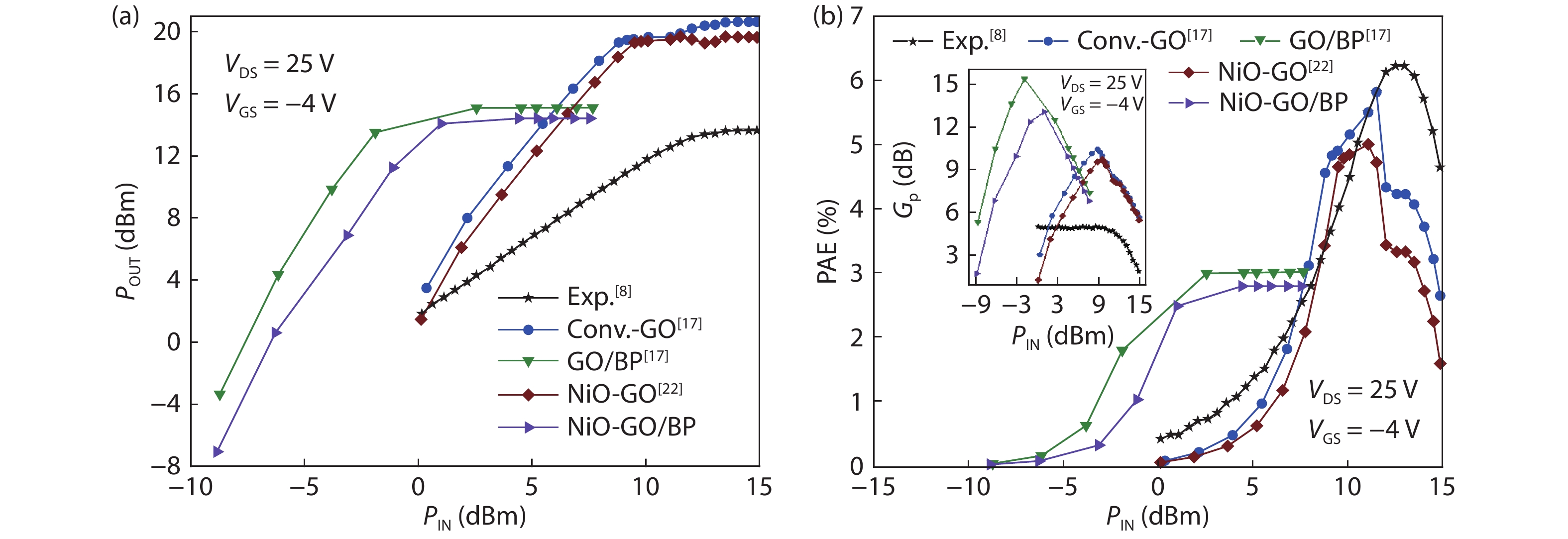
The radio-frequency (RF) performance of the p-type NiO-pocket based β-Ga2O3/black phosphorous heterostructure MOSFET has been evaluated. The key figure of merits (FOMs) for device performance evaluation include the transconductance (gm) gate dependent intrinsic-capacitances (Cgd and Cgs), cutoff frequency (fT), gain bandwidth (GBW) product and output-conductance (gd). Similarly, power-gain (Gp), power added efficiency (PAE), and output power (POUT) are also investigated for large-signal continuous-wave (CW) RF performance evaluation. The motive behind the study is to improve the β-Ga2O3 MOS device performance along with a reduction in power losses and device associated leakages. To show the applicability of the designed device in RF applications, its RF FOMs are analyzed. With the outline characteristics of the ultrathin black phosphorous layer below the β-Ga2O3 channel region, the proposed device results in 1.09 times improvement in fT, with 0.7 times lower Cgs, and 3.27 dB improved GP in comparison to the NiO-GO MOSFET. The results indicate that the designed NiO-GO/BP MOSFET has better RF performance with improved power gain and low leakages.