Issue Browser
Volume 44, Issue 9,
Sep 2023
J. Semicond.
2023, 44(9): 091601 doi: 10.1088/1674-4926/44/9/091601
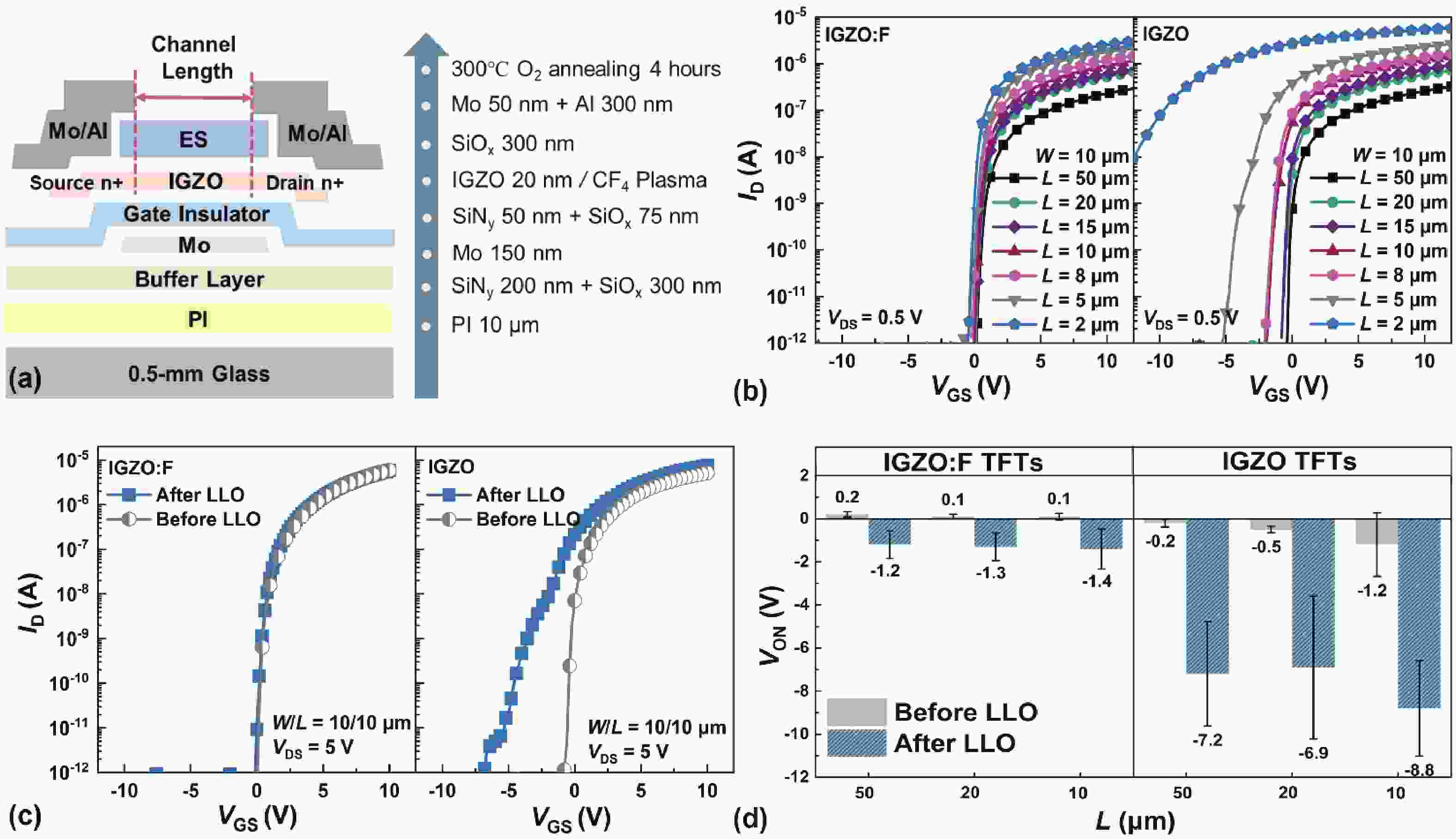
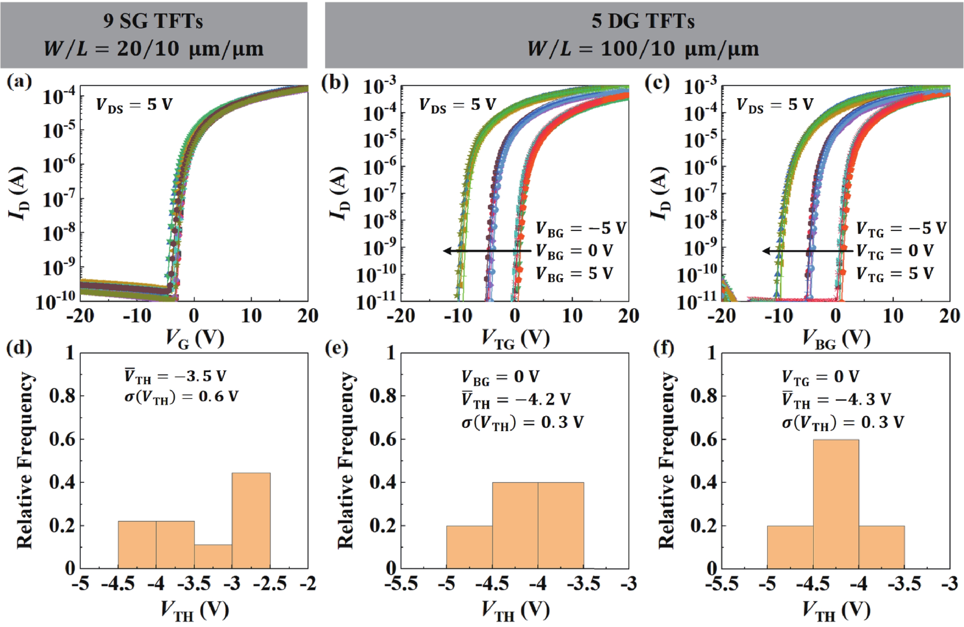
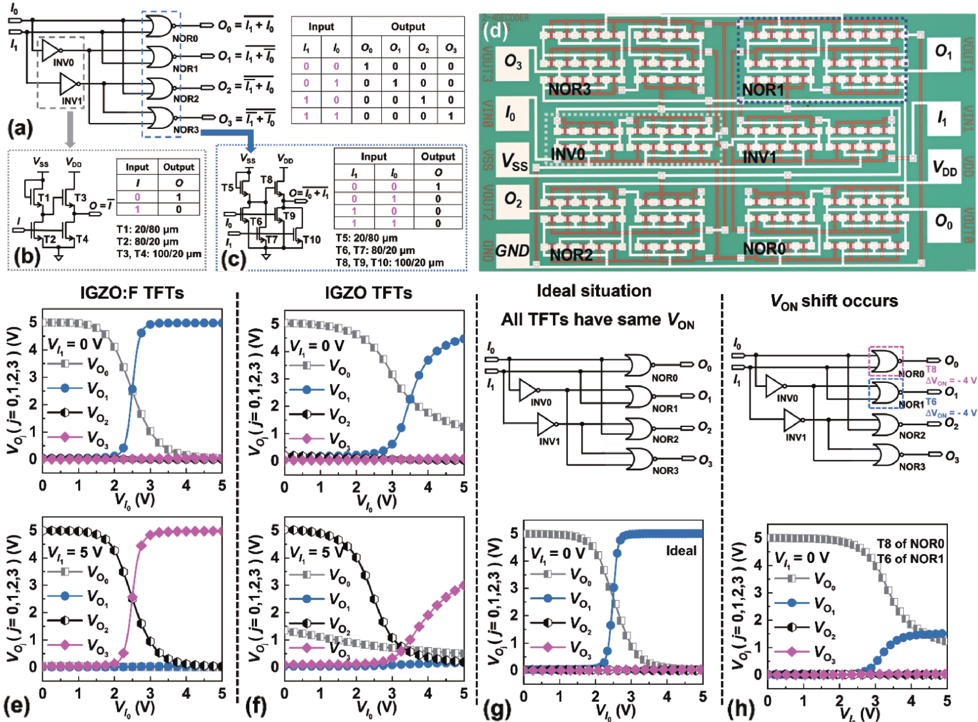
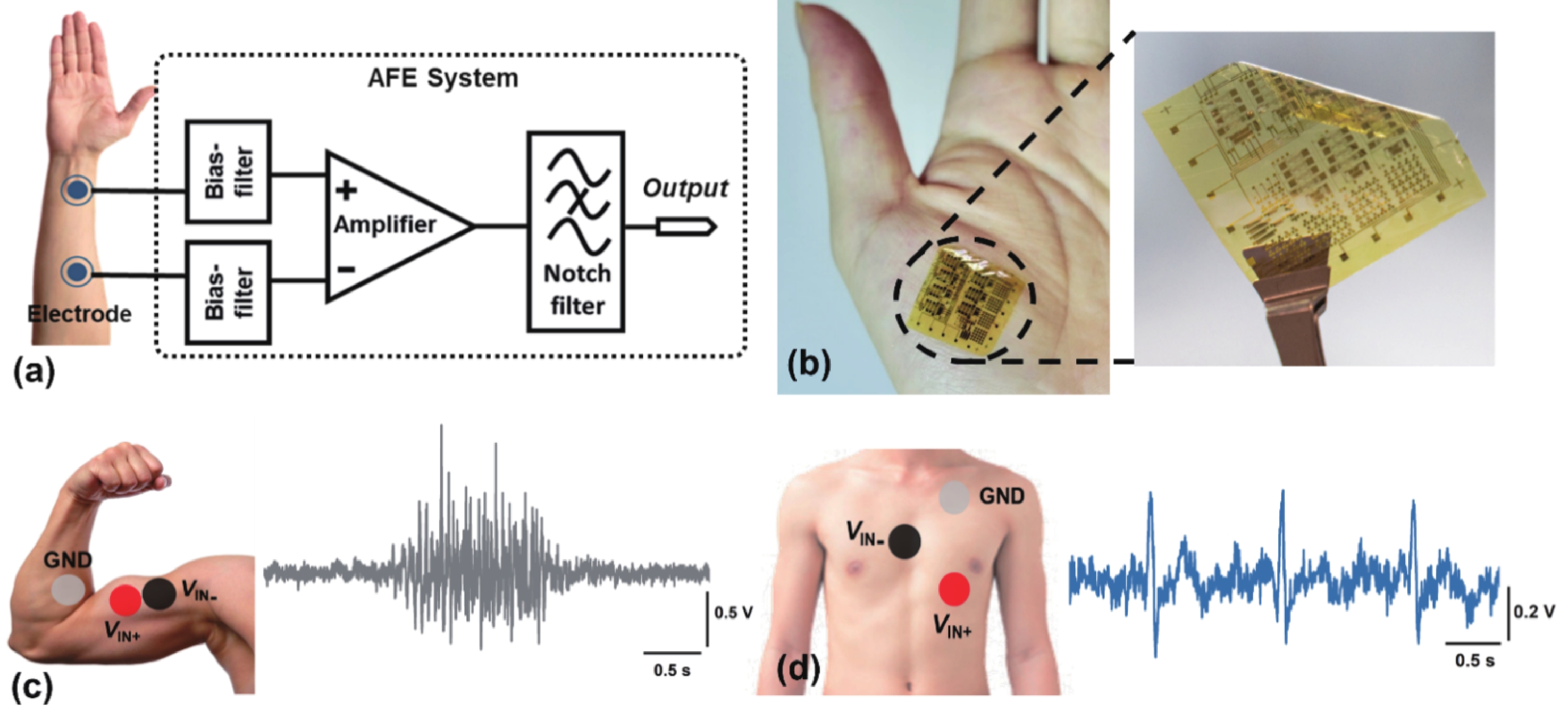
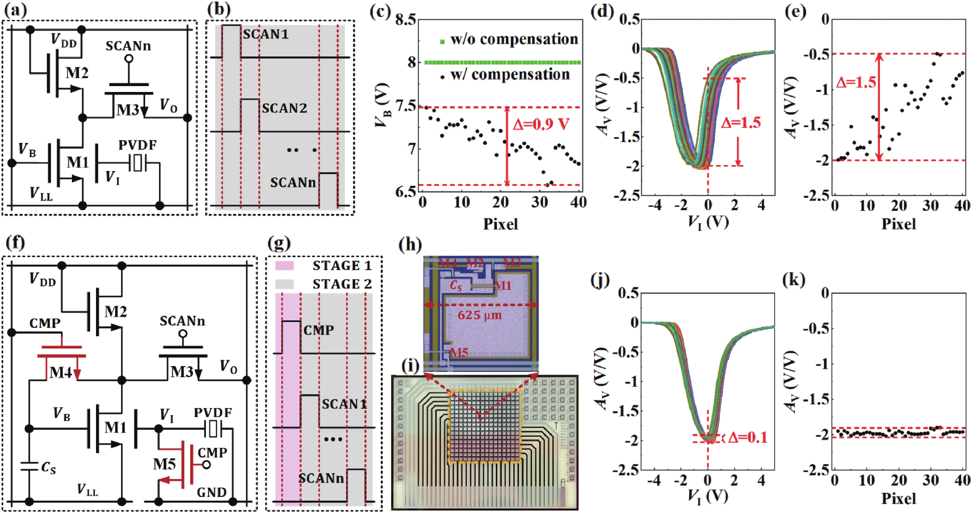
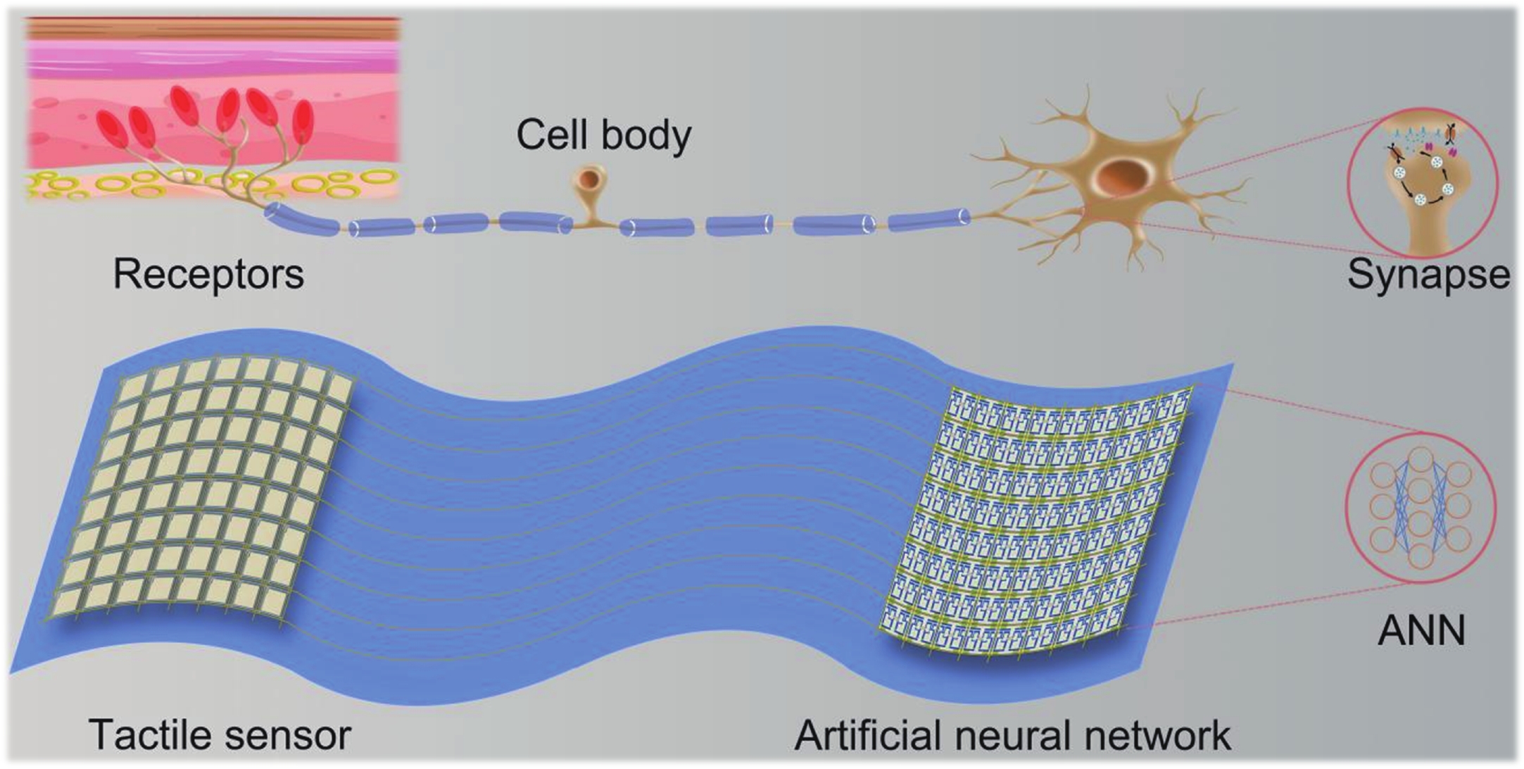
Here we review two 300 °C metal–oxide (MO) thin-film transistor (TFT) technologies for the implementation of flexible electronic circuits and systems. Fluorination-enhanced TFTs for suppressing the variation and shift of turn-on voltage (VON), and dual-gate TFTs for acquiring sensor signals and modulating VON have been deployed to improve the robustness and performance of the systems in which they are deployed. Digital circuit building blocks based on fluorinated TFTs have been designed, fabricated, and characterized, which demonstrate the utility of the proposed low-temperature TFT technologies for implementing flexible electronic systems. The construction and characterization of an analog front-end system for the acquisition of bio-potential signals and an active-matrix sensor array for the acquisition of tactile images have been reported recently.


J. Semicond.
2023, 44(9): 091602 doi: 10.1088/1674-4926/44/9/091602

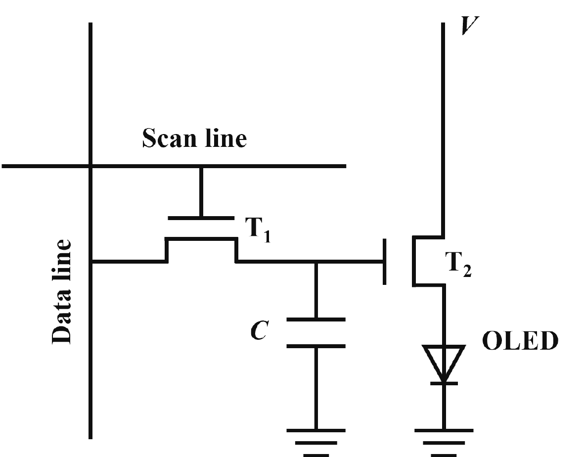
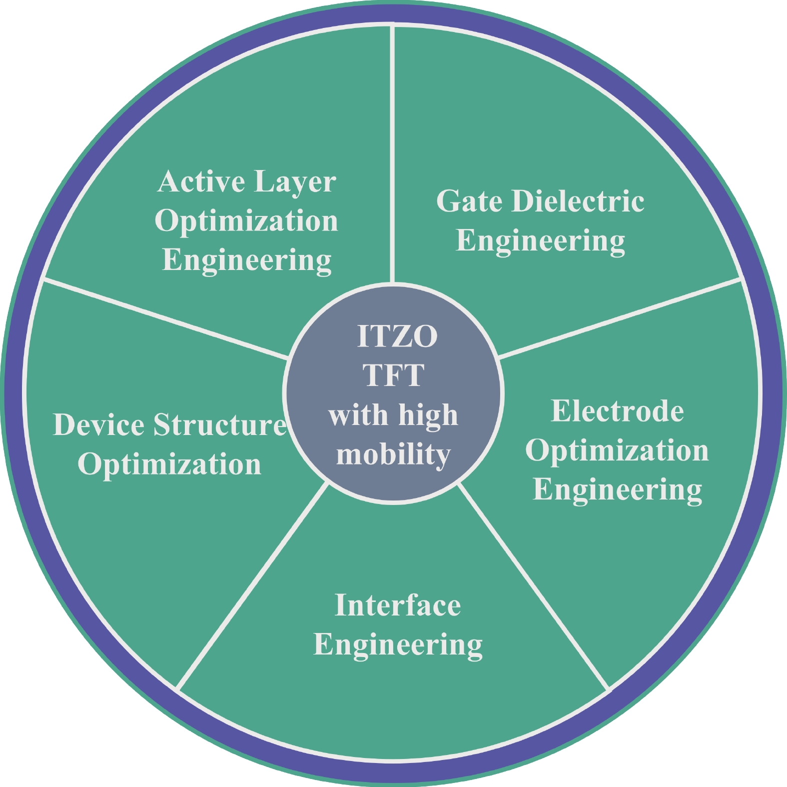
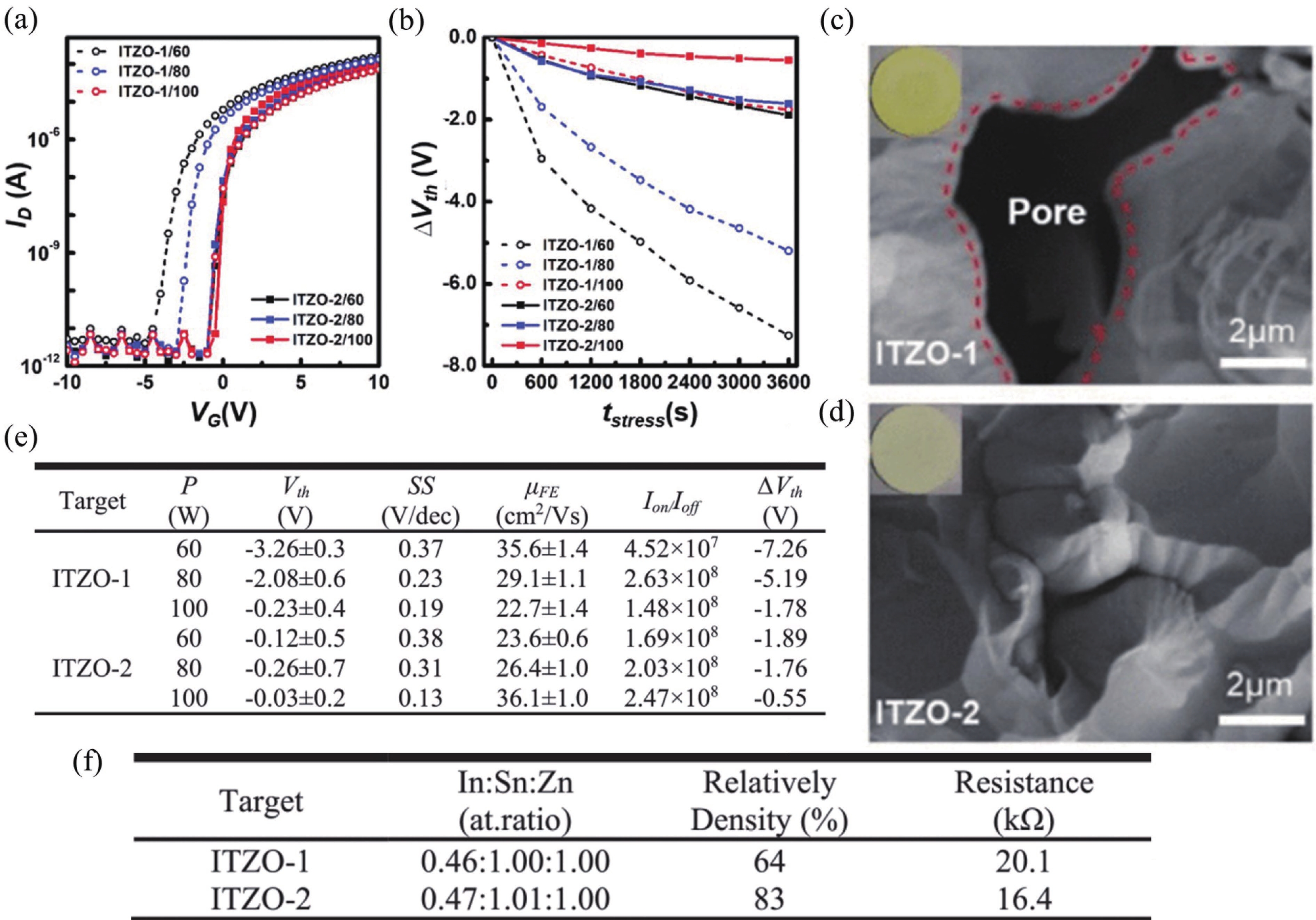
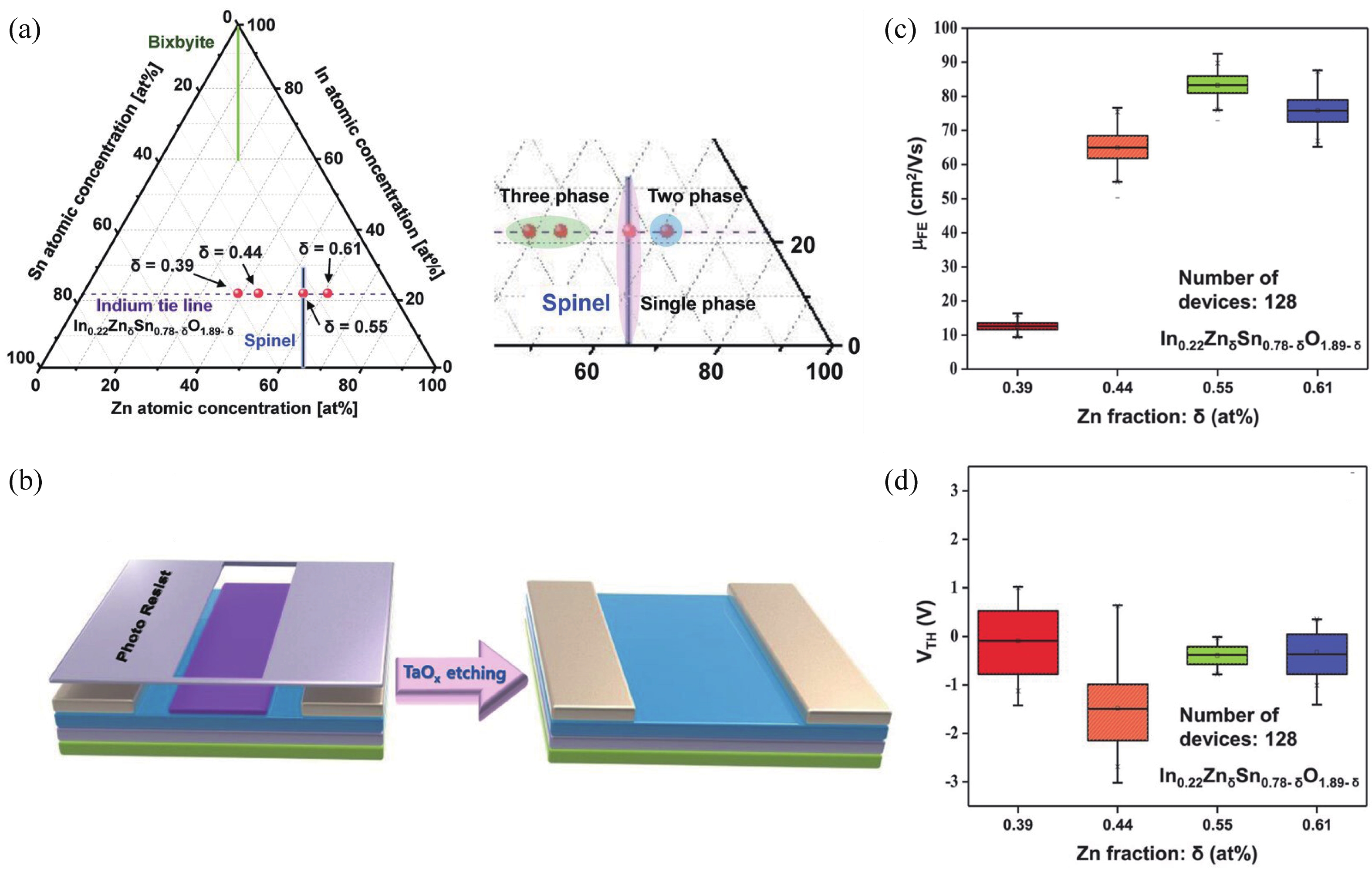
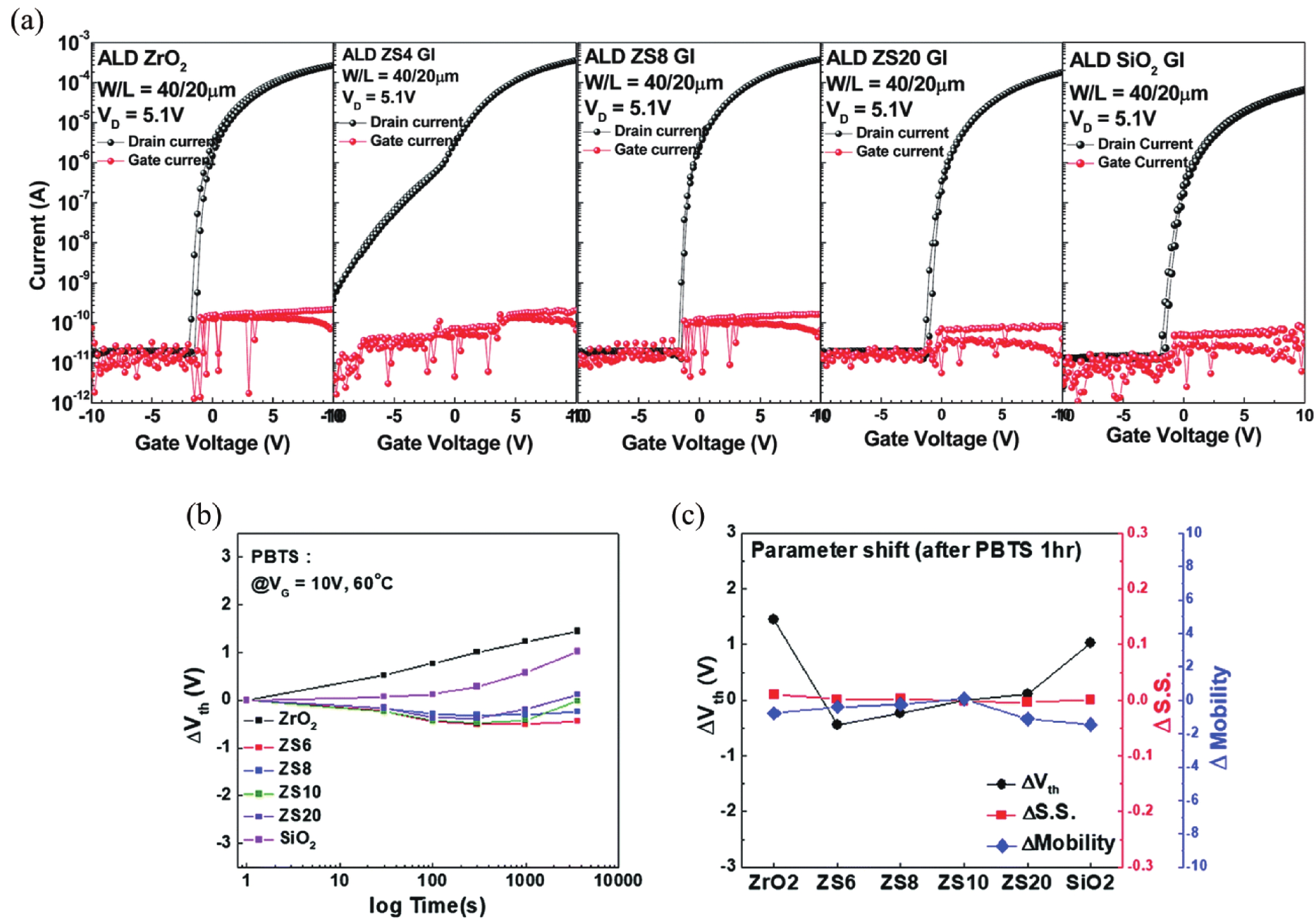
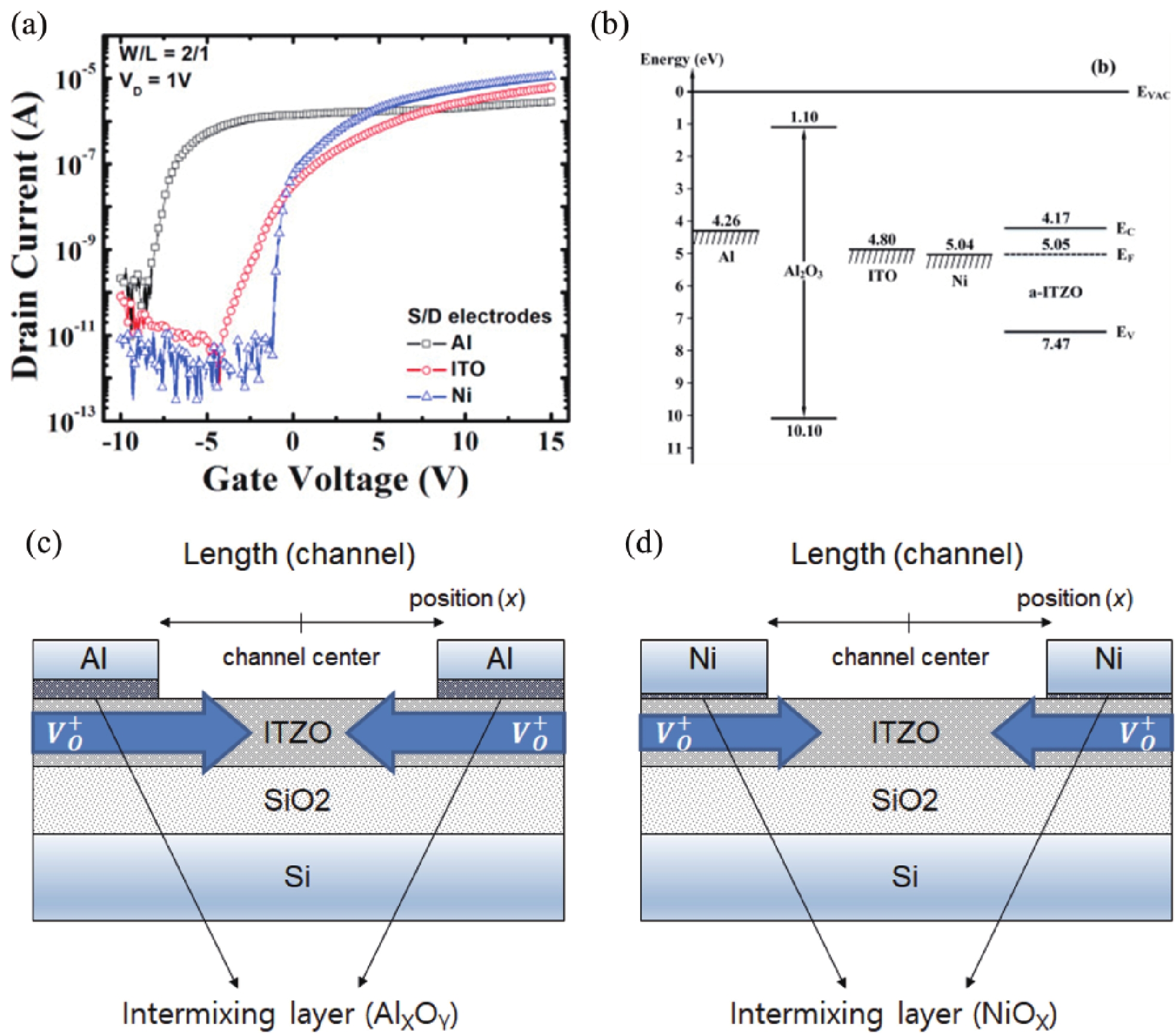
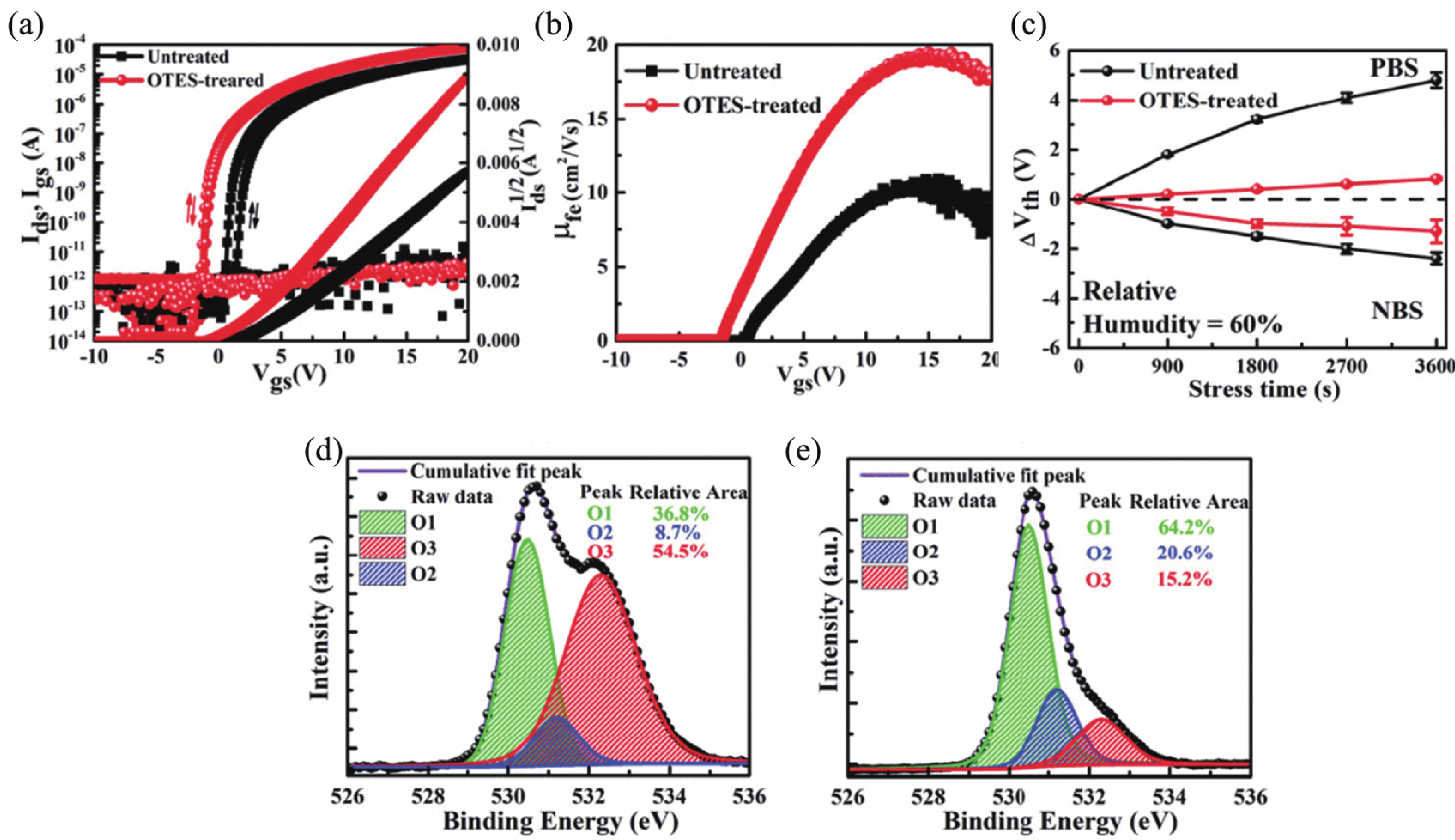
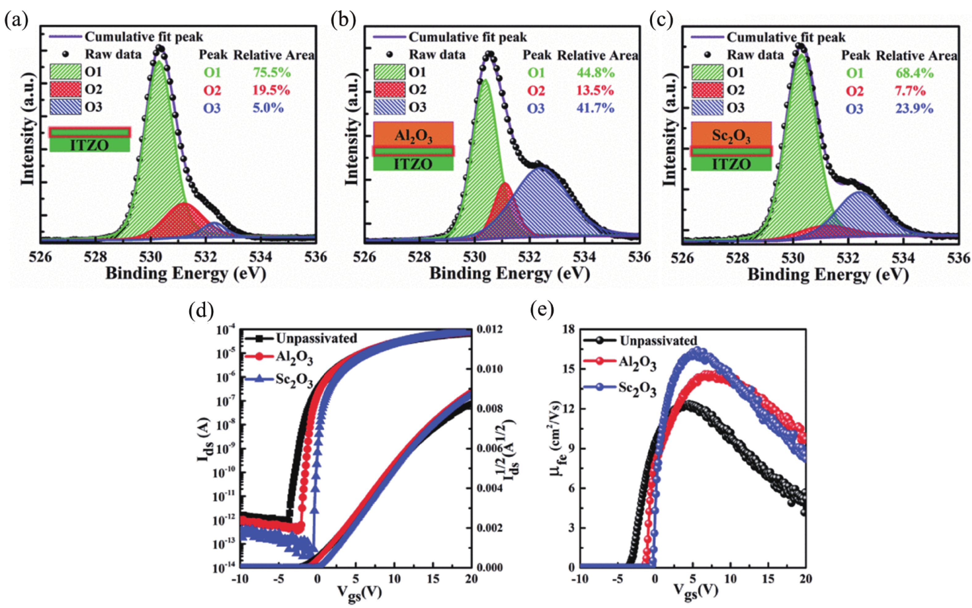
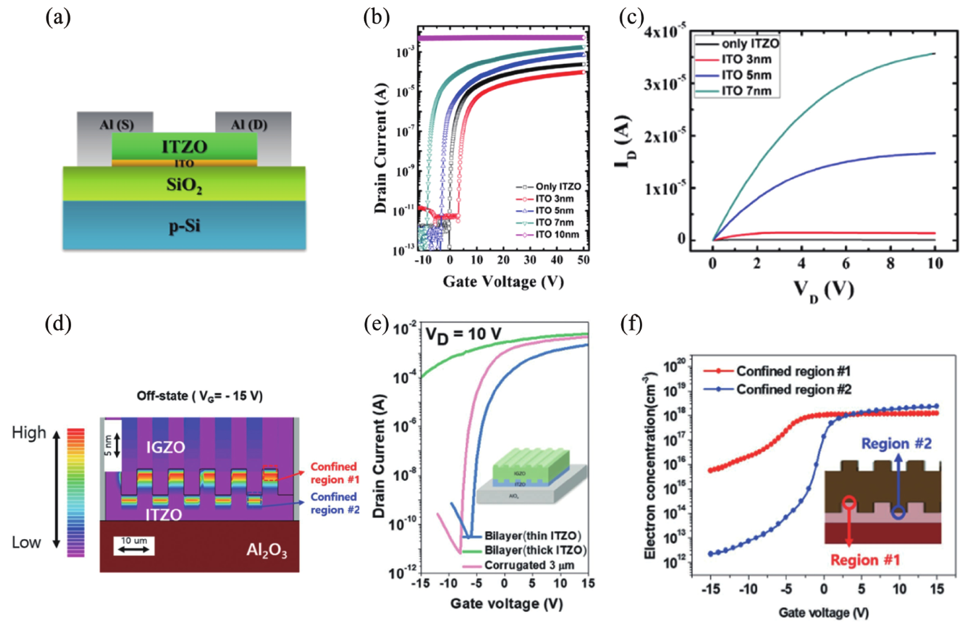
Indium-tin-zinc oxide (ITZO) thin-film transistor (TFT) technology holds promise for achieving high mobility and offers significant opportunities for commercialization. This paper provides a review of progress made in improving the mobility of ITZO TFTs. This paper begins by describing the development and current status of metal-oxide TFTs, and then goes on to explain the advantages of selecting ITZO as the TFT channel layer. The evaluation criteria for TFTs are subsequently introduced, and the reasons and significance of enhancing mobility are clarified. This paper then explores the development of high-mobility ITZO TFTs from five perspectives: active layer optimization, gate dielectric optimization, electrode optimization, interface optimization, and device structure optimization. Finally, a summary and outlook of the research field are presented.


J. Semicond.
2023, 44(9): 091603 doi: 10.1088/1674-4926/44/9/091603
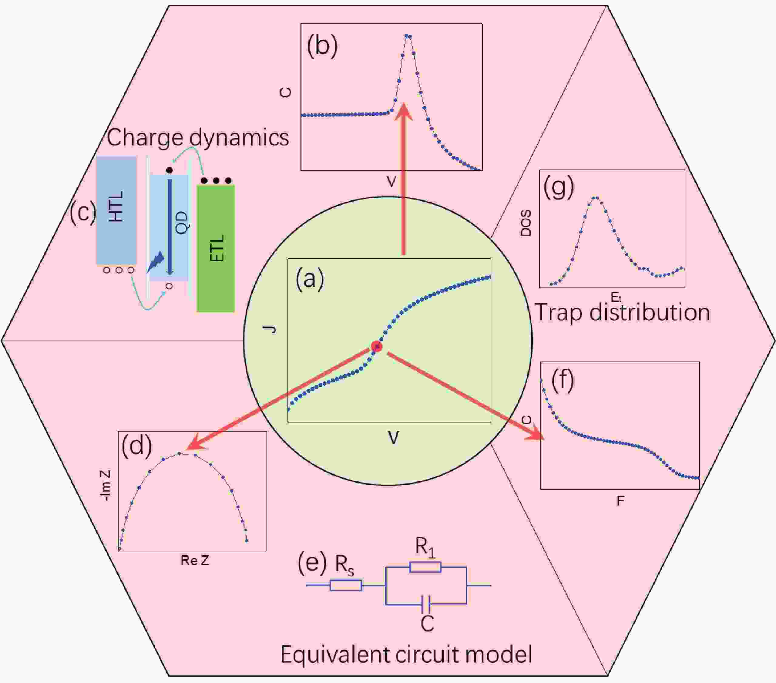
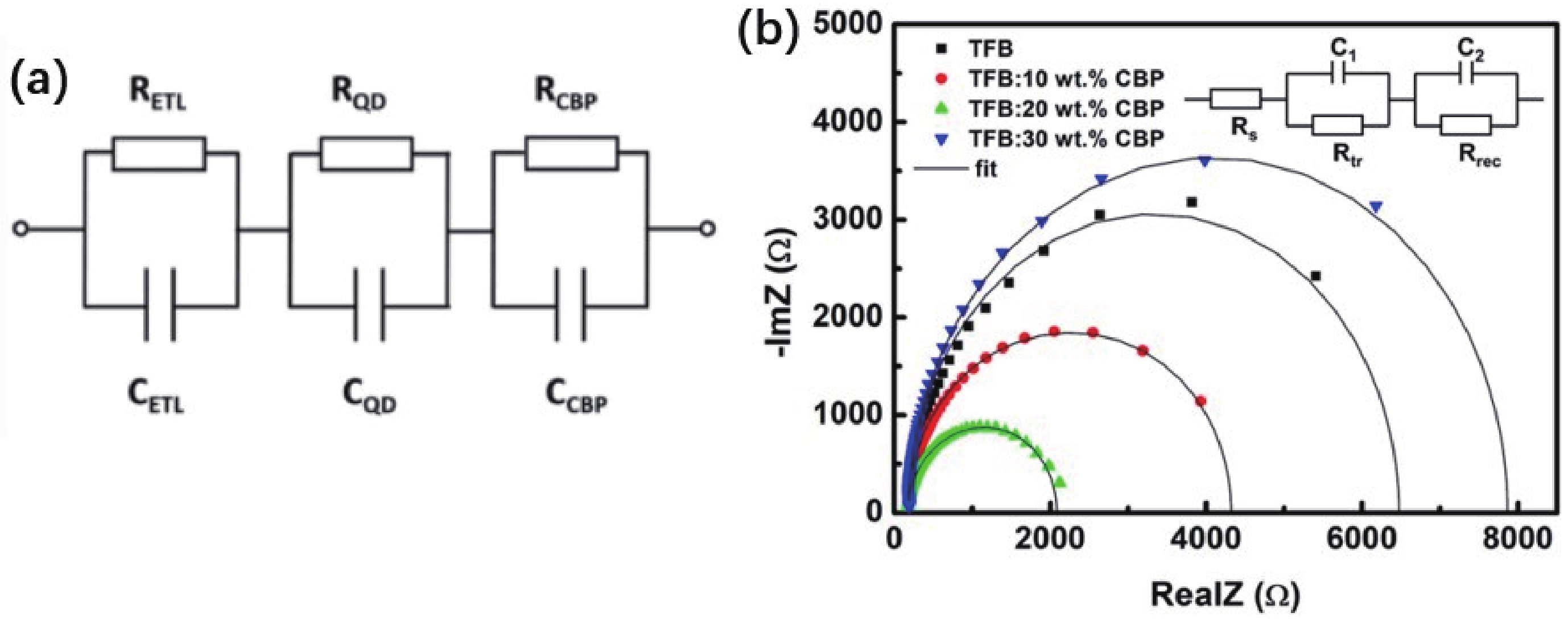
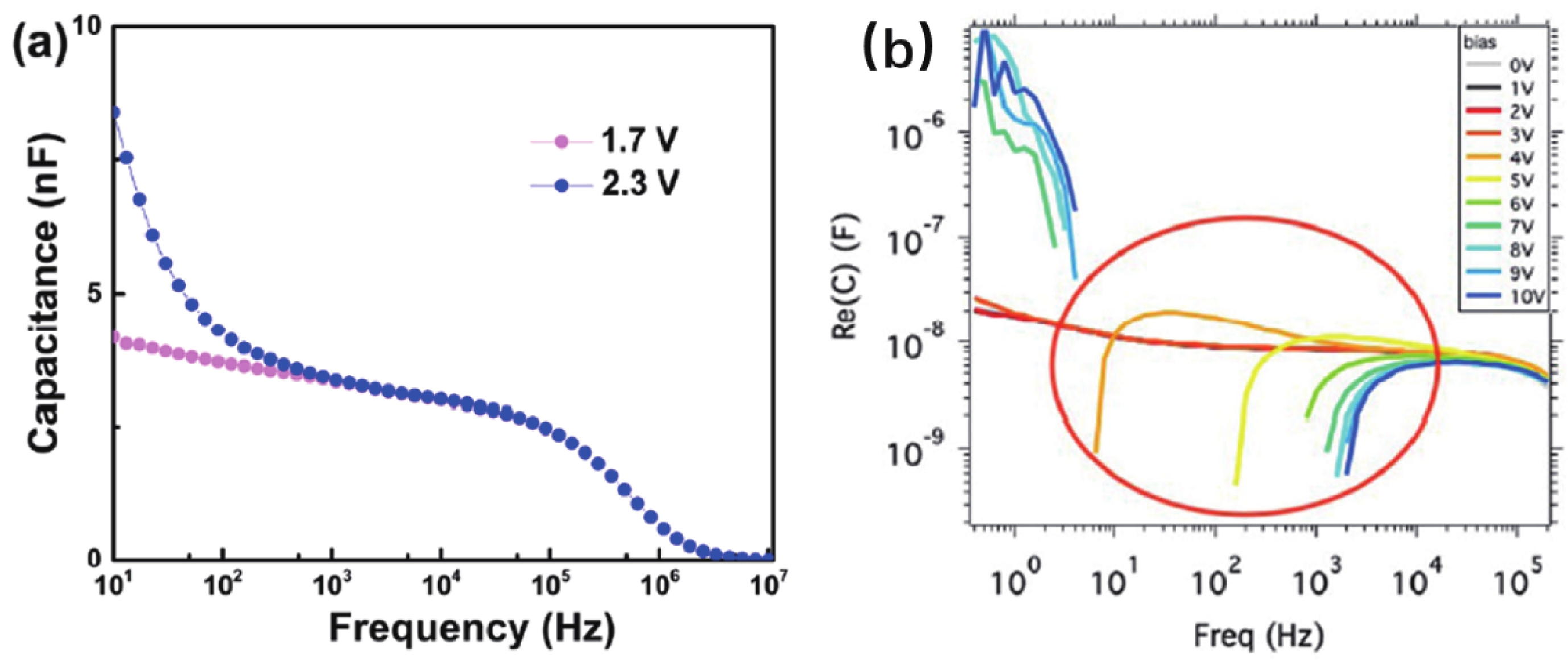
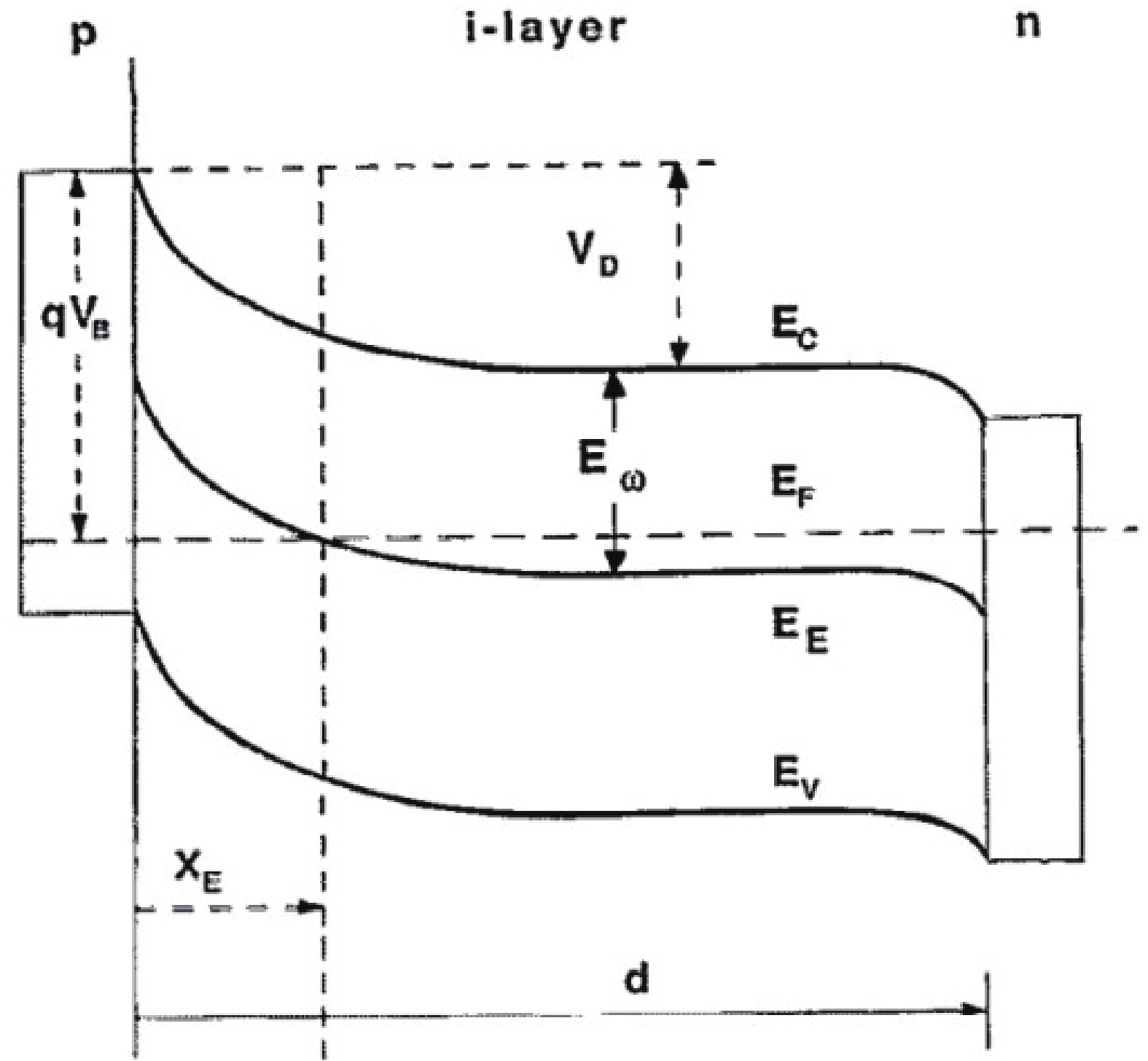
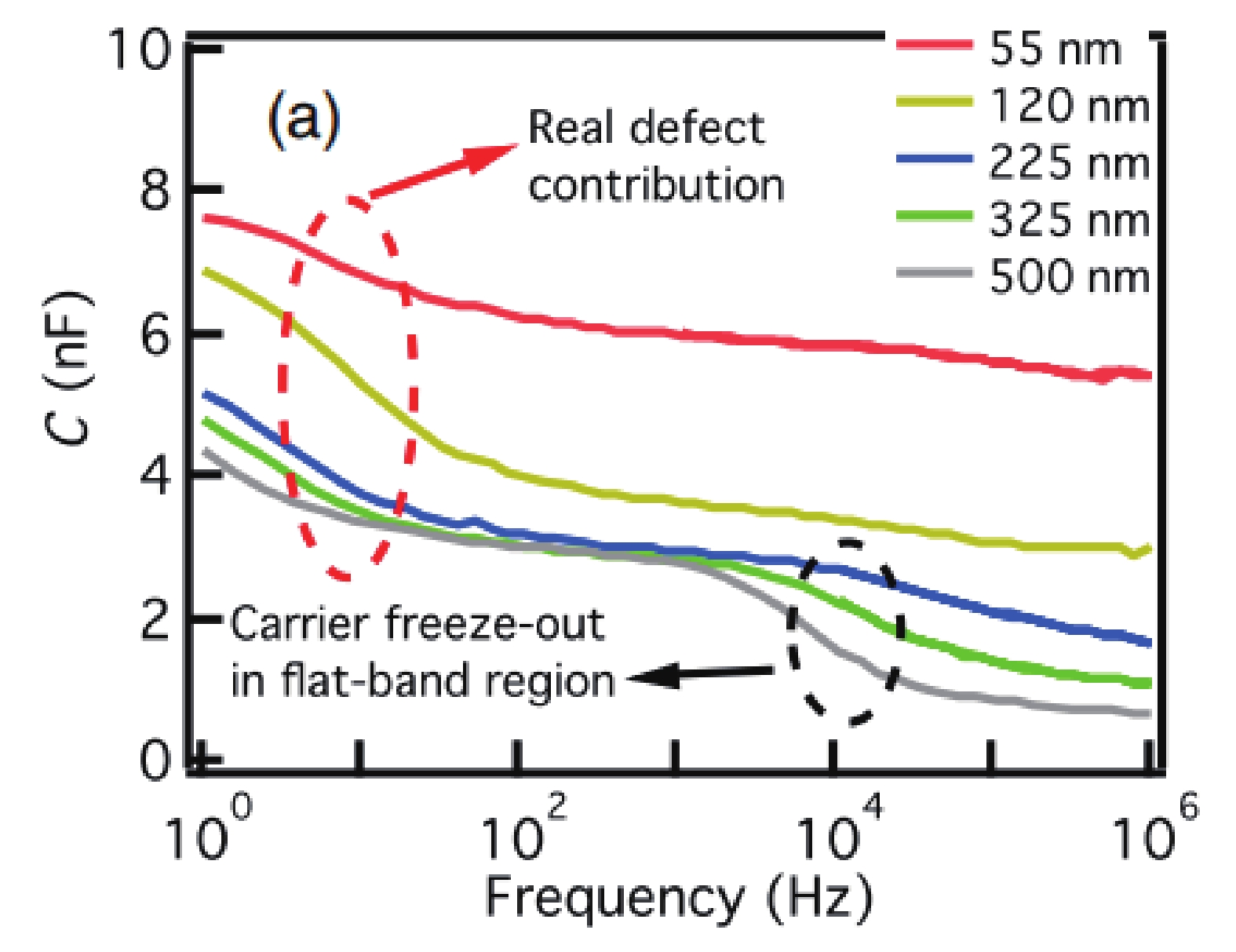
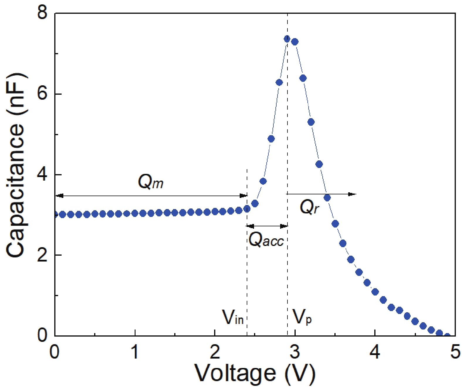
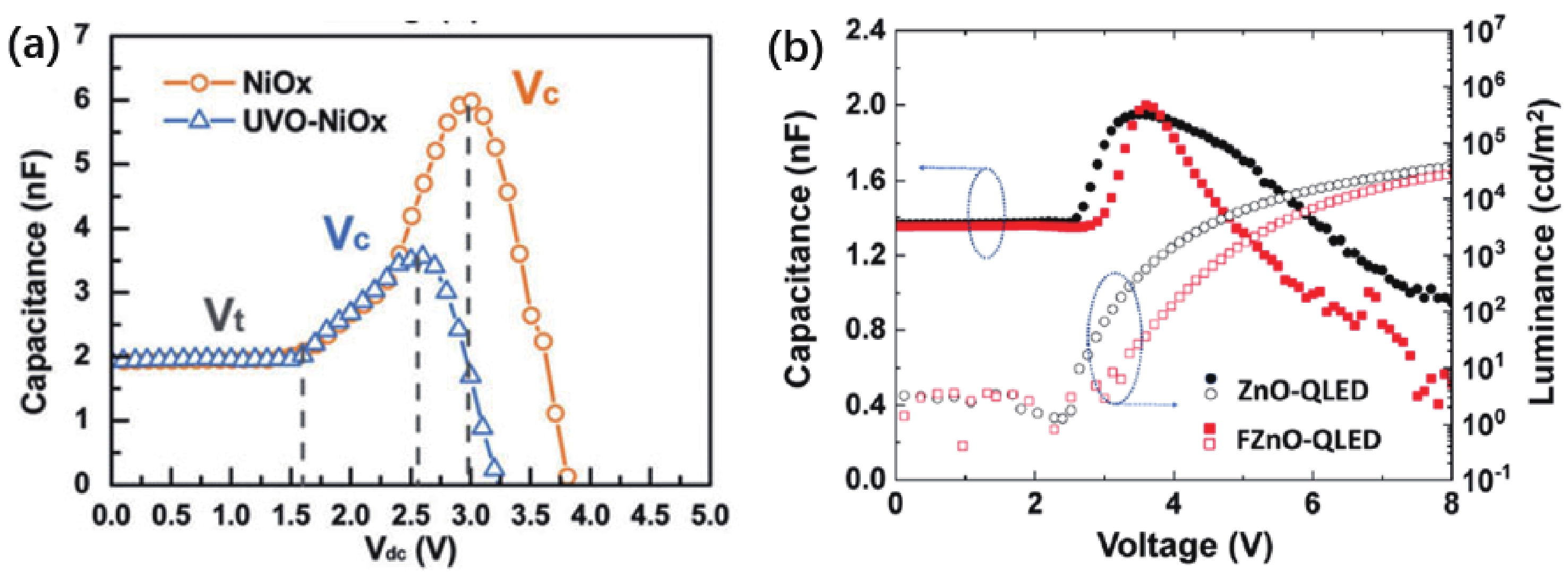
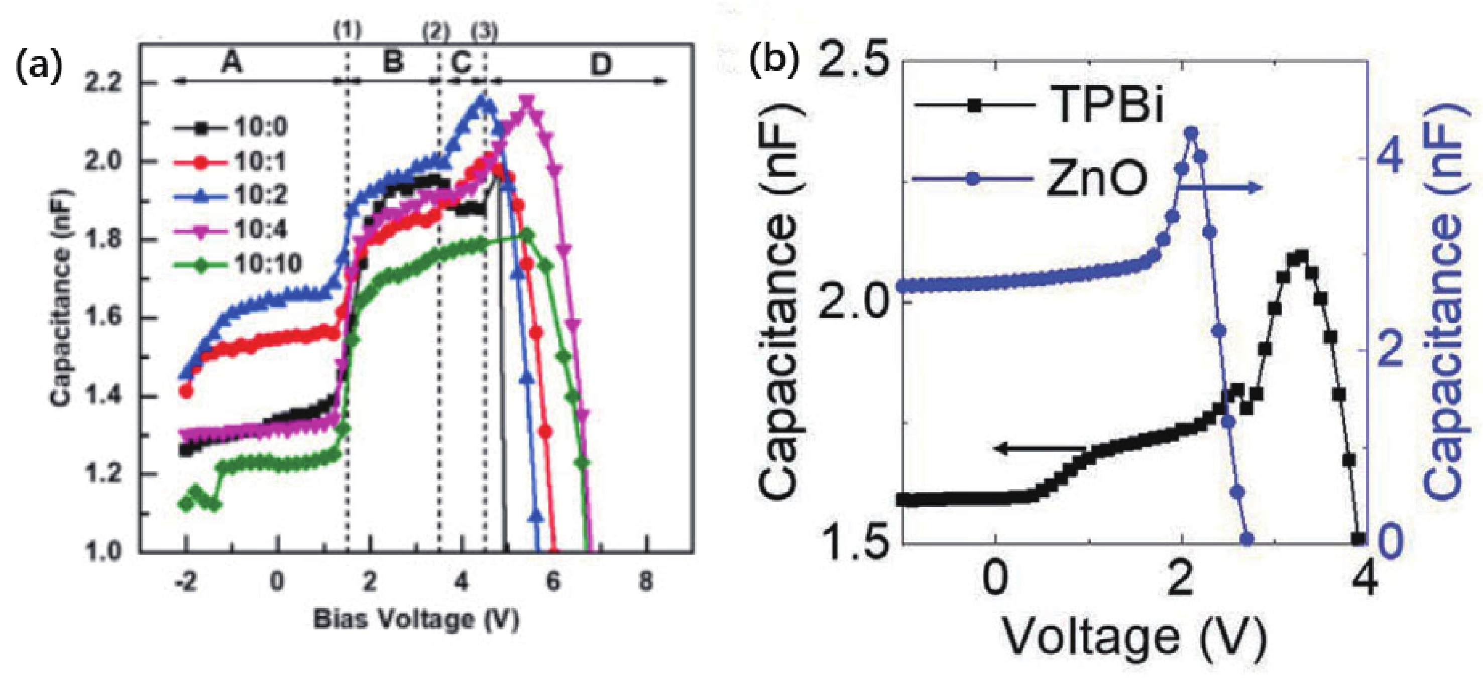
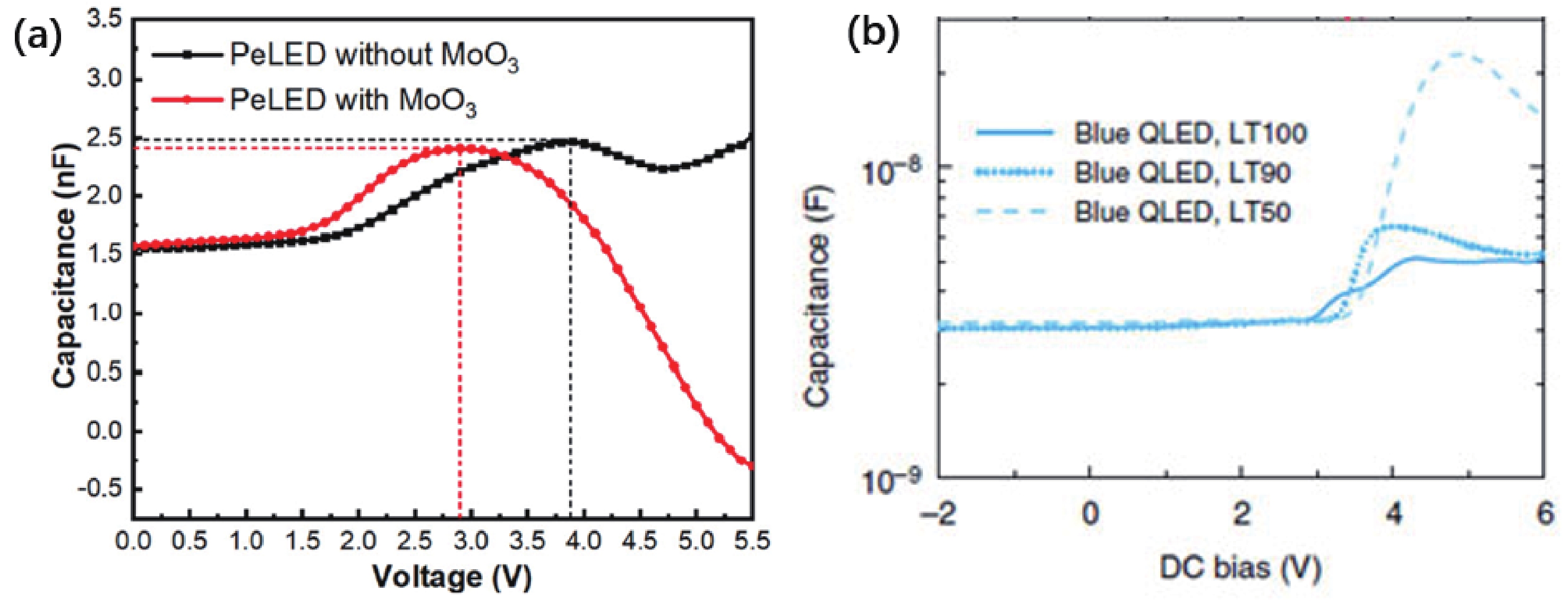
Impedance spectroscopy has been increasingly employed in quantum dot light-emitting diodes (QLEDs) to investigate the charge dynamics and device physics. In this review, we introduce the mathematical basics of impedance spectroscopy that applied to QLEDs. In particular, we focus on the Nyquist plot, Mott−Schottky analysis, capacitance-frequency and capacitance-voltage characteristics, and the dC/dV measurement of the QLEDs. These impedance measurements can provide critical information on electrical parameters such as equivalent circuit models, characteristic time constants, charge injection and recombination points, and trap distribution of the QLEDs. However, this paper will also discuss the disadvantages and limitations of these measurements. Fundamentally, this review provides a deeper understanding of the device physics of QLEDs through the application of impedance spectroscopy, offering valuable insights into the analysis of performance loss and degradation mechanisms of QLEDs.


J. Semicond.
2023, 44(9): 091604 doi: 10.1088/1674-4926/44/9/091604
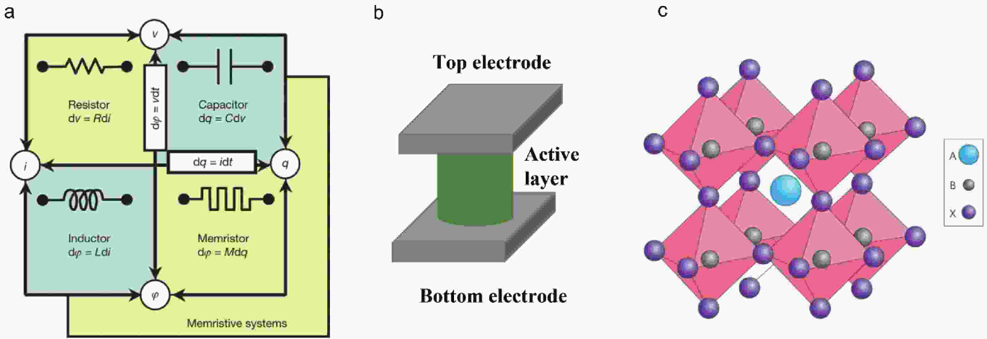
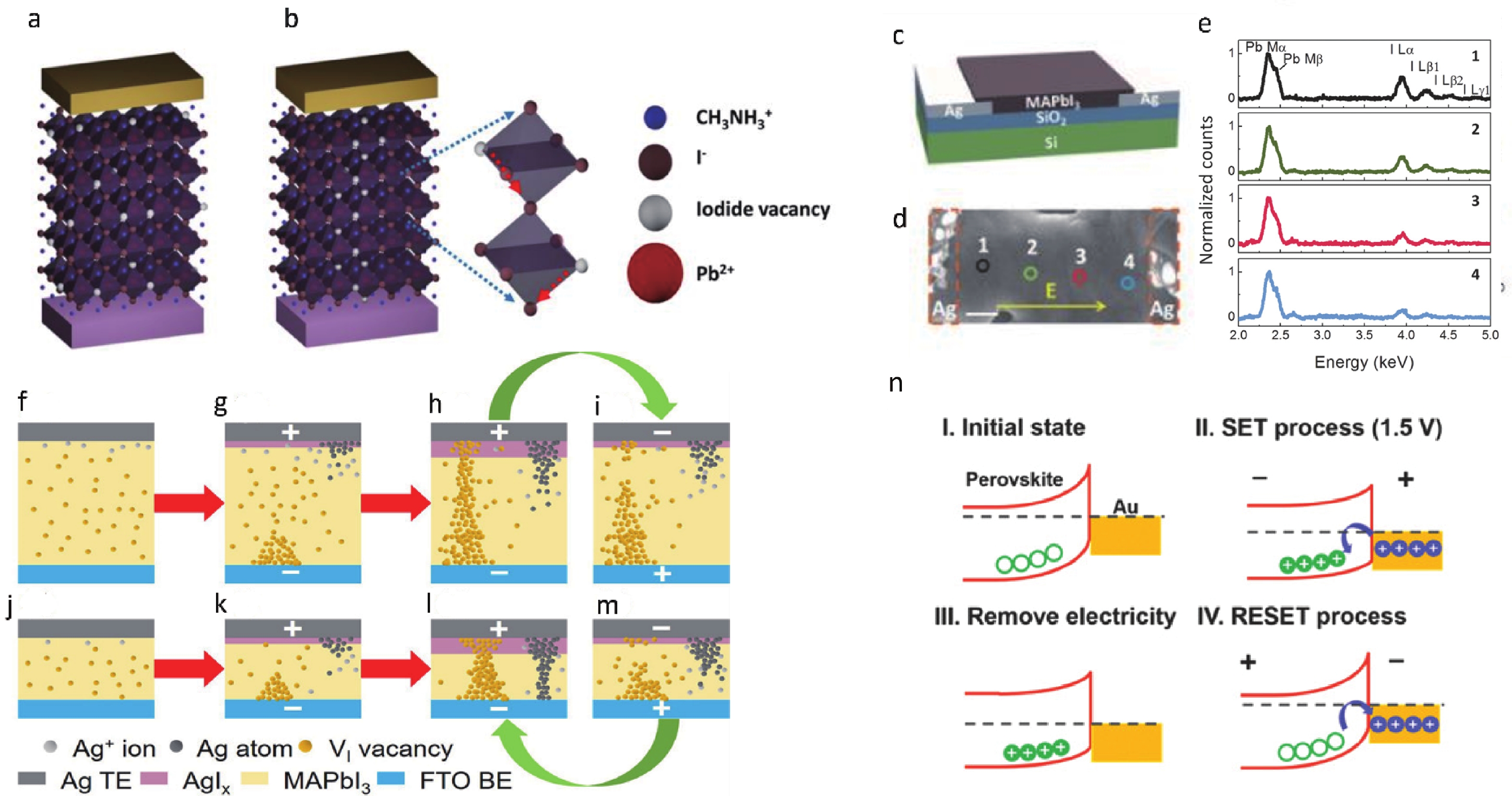
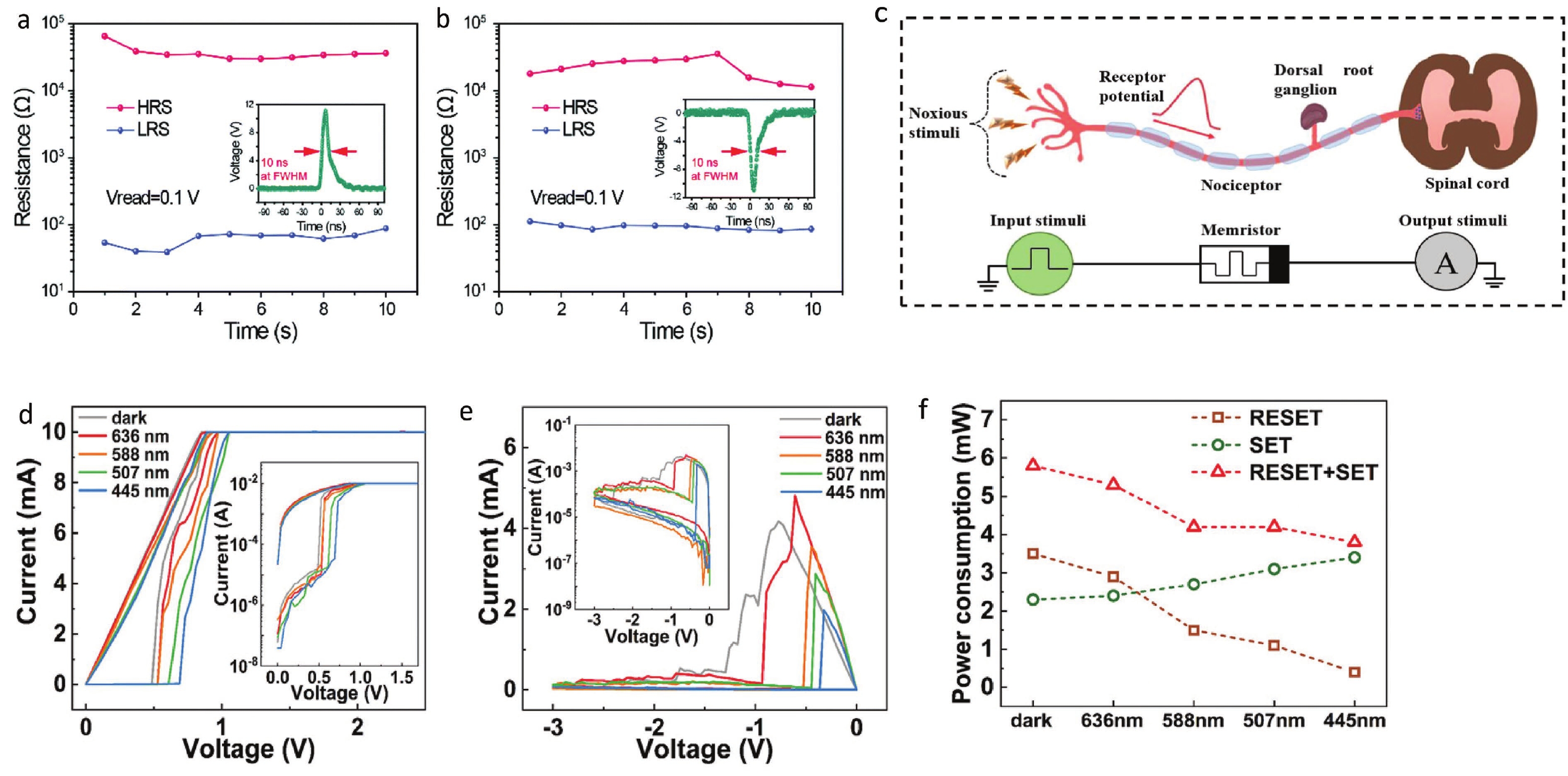
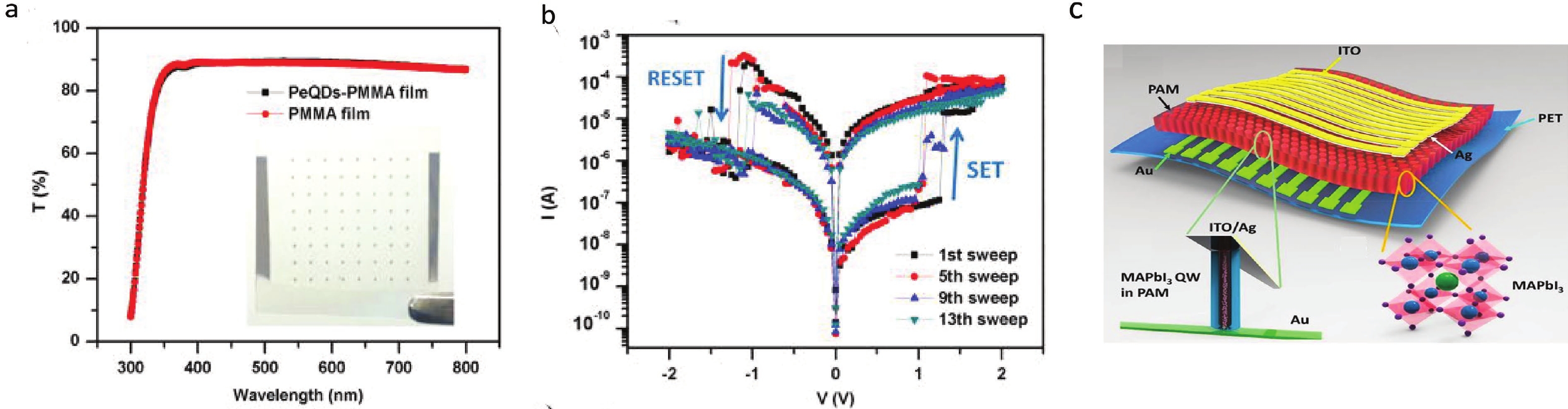
Organic-inorganic halides perovskites (OHPs) have drawn the attention of many researchers owing to their astonishing and unique optoelectronic properties. They have been extensively used for photovoltaic applications, achieving higher than 26% power conversion efficiency to date. These materials have potential to be deployed for many other applications beyond photovoltaics like photodetectors, sensors, light-emitting diodes (LEDs), and resistors. To address the looming challenge of Moore's law and the Von Neumann bottleneck, many new technologies regarding the computation of architectures and storage of information are being extensively researched. Since the discovery of the memristor as a fourth component of the circuit, many materials are explored for memristive applications. Lately, researchers have advanced the exploration of OHPs for memristive applications. These materials possess promising memristive properties and various kinds of halide perovskites have been used for different applications that are not only limited to data storage but expand towards artificial synapses, and neuromorphic computing. Herein we summarize the recent advancements of OHPs for memristive applications, their unique electronic properties, fabrication of materials, and current progress in this field with some future perspectives and outlooks.


J. Semicond.
2023, 44(9): 091605 doi: 10.1088/1674-4926/44/9/091605
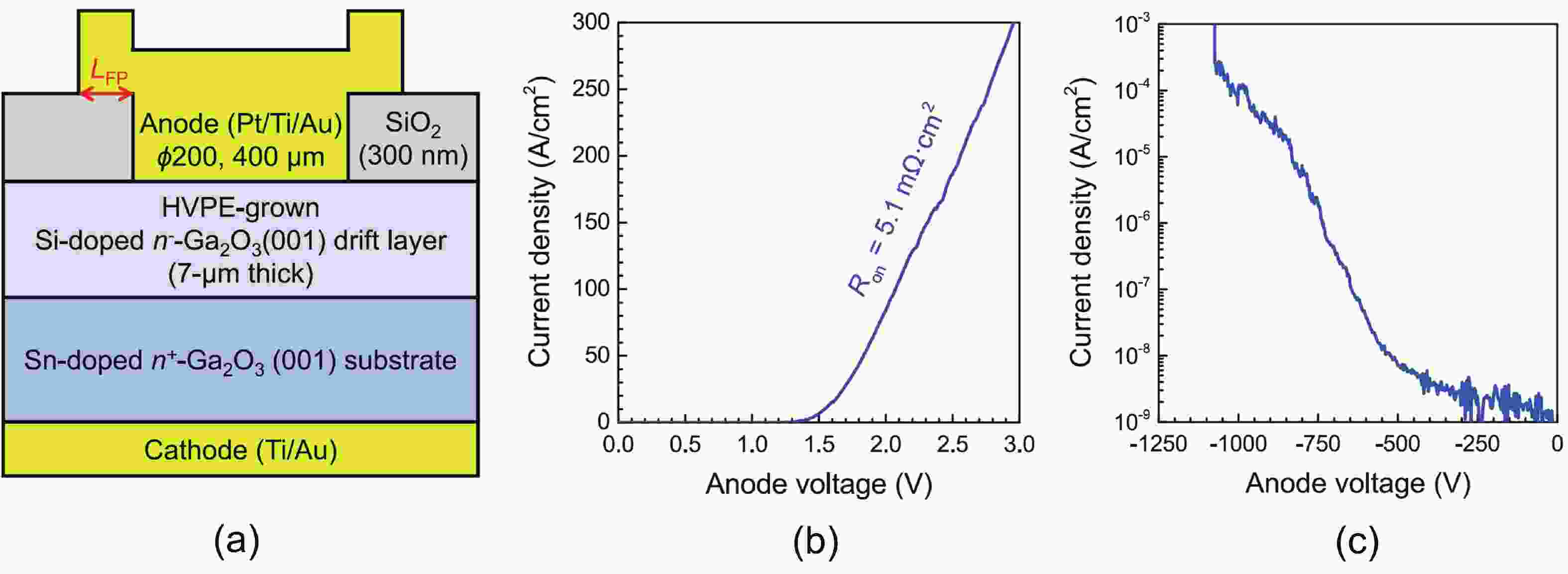
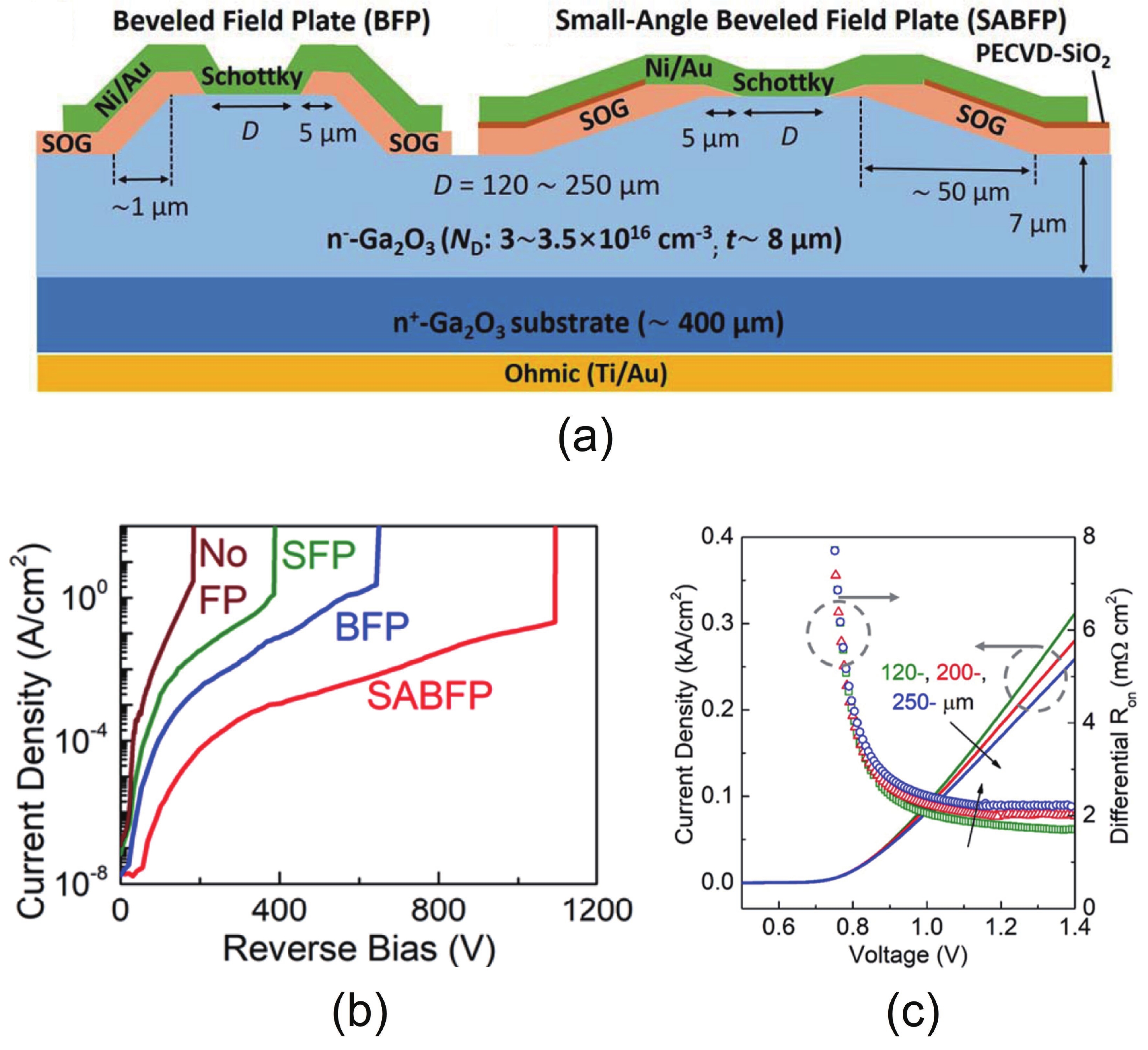
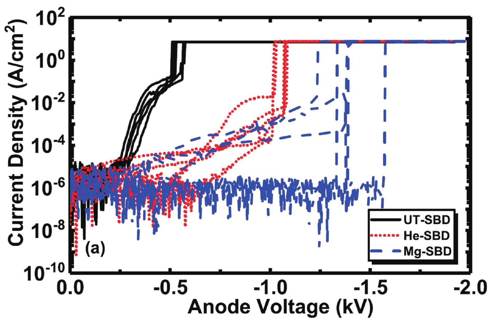
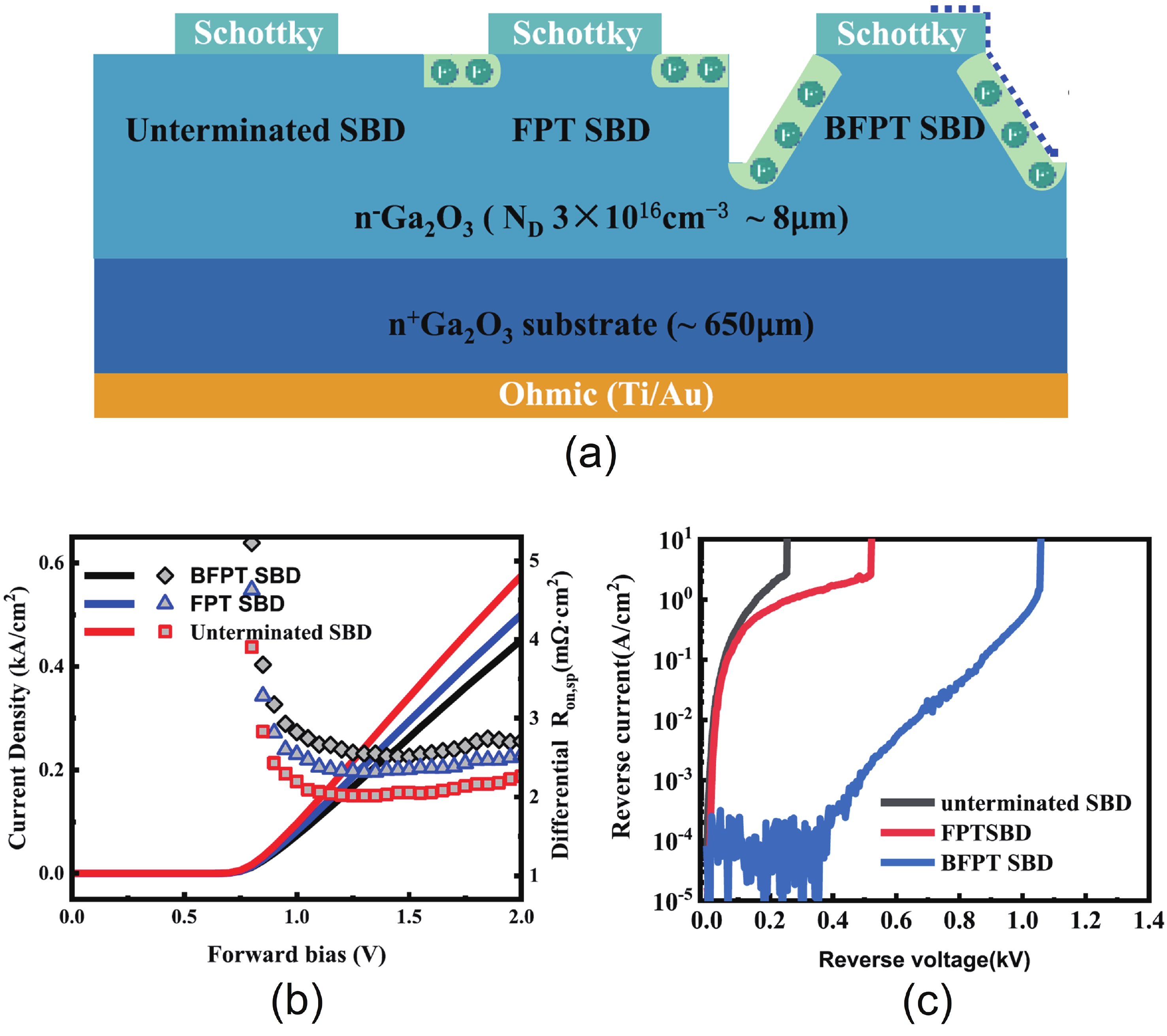
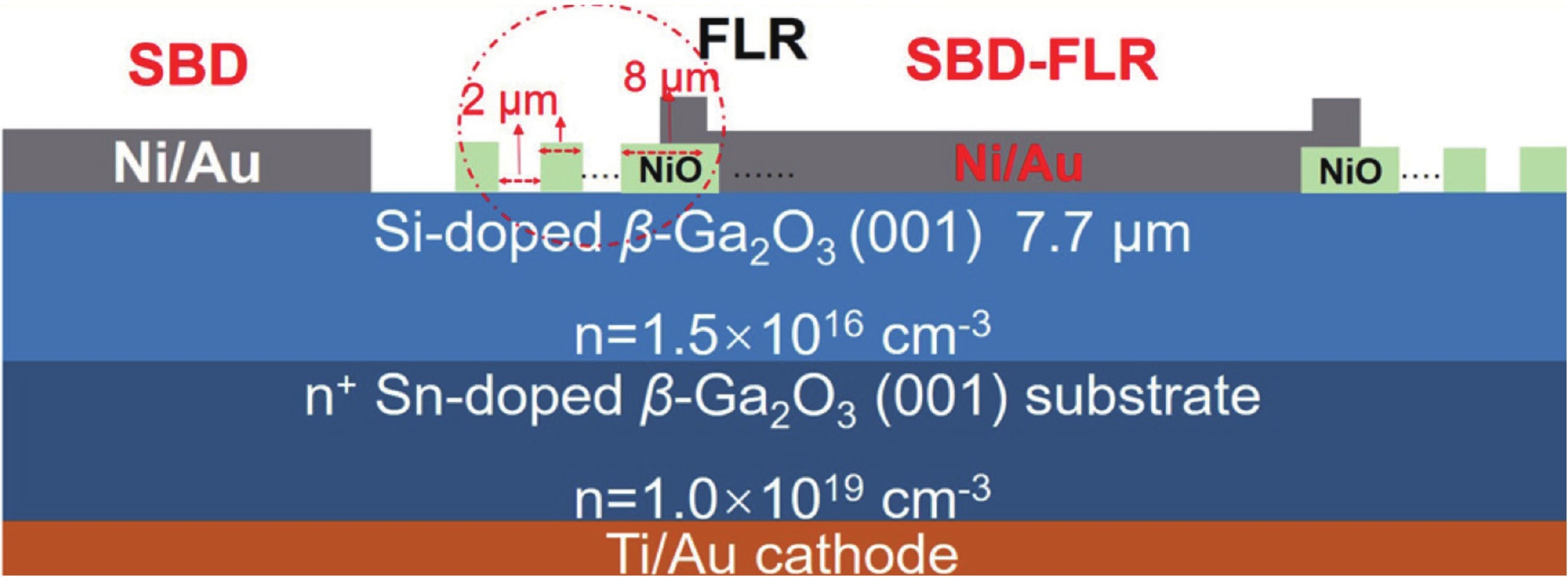
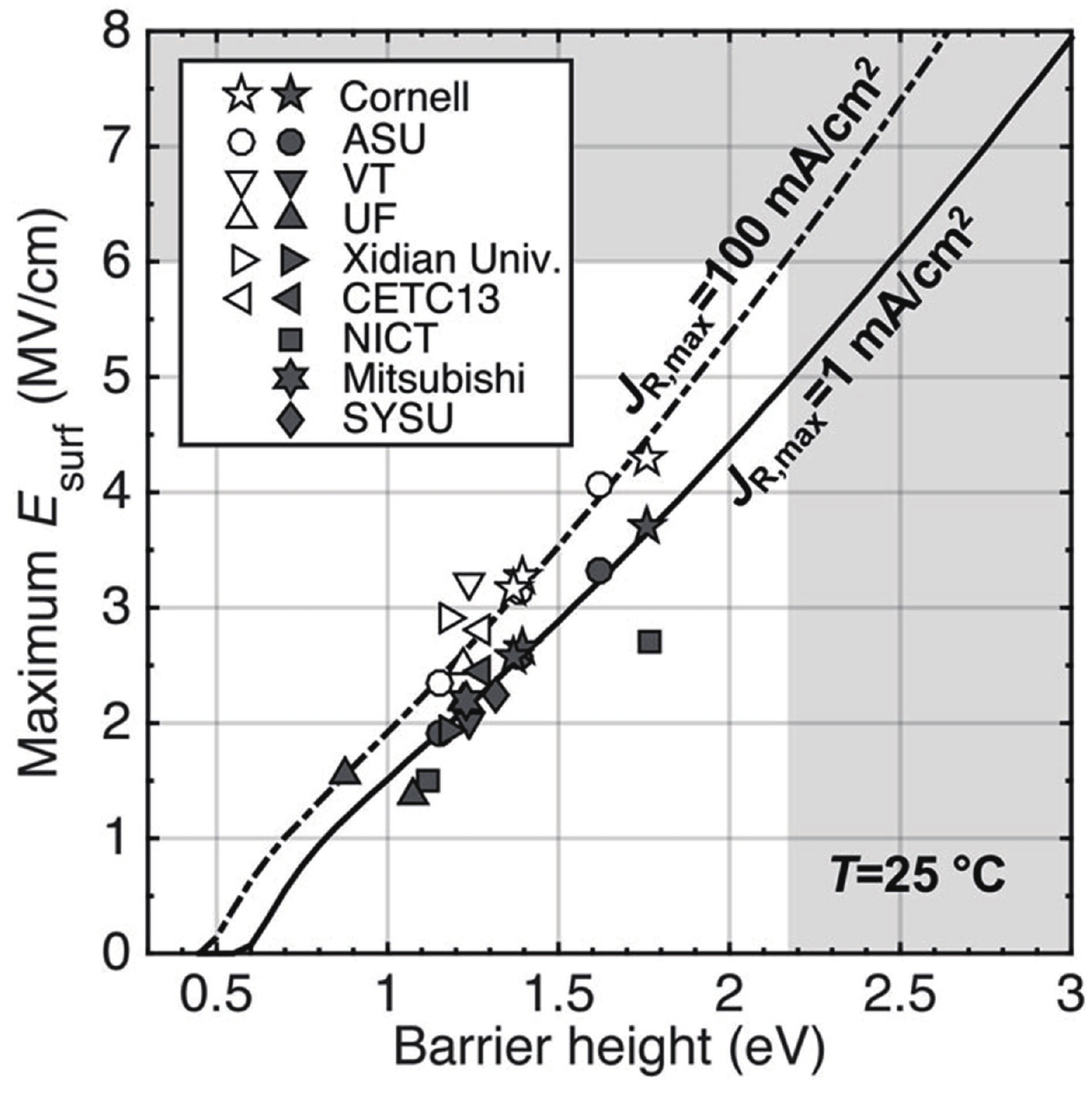
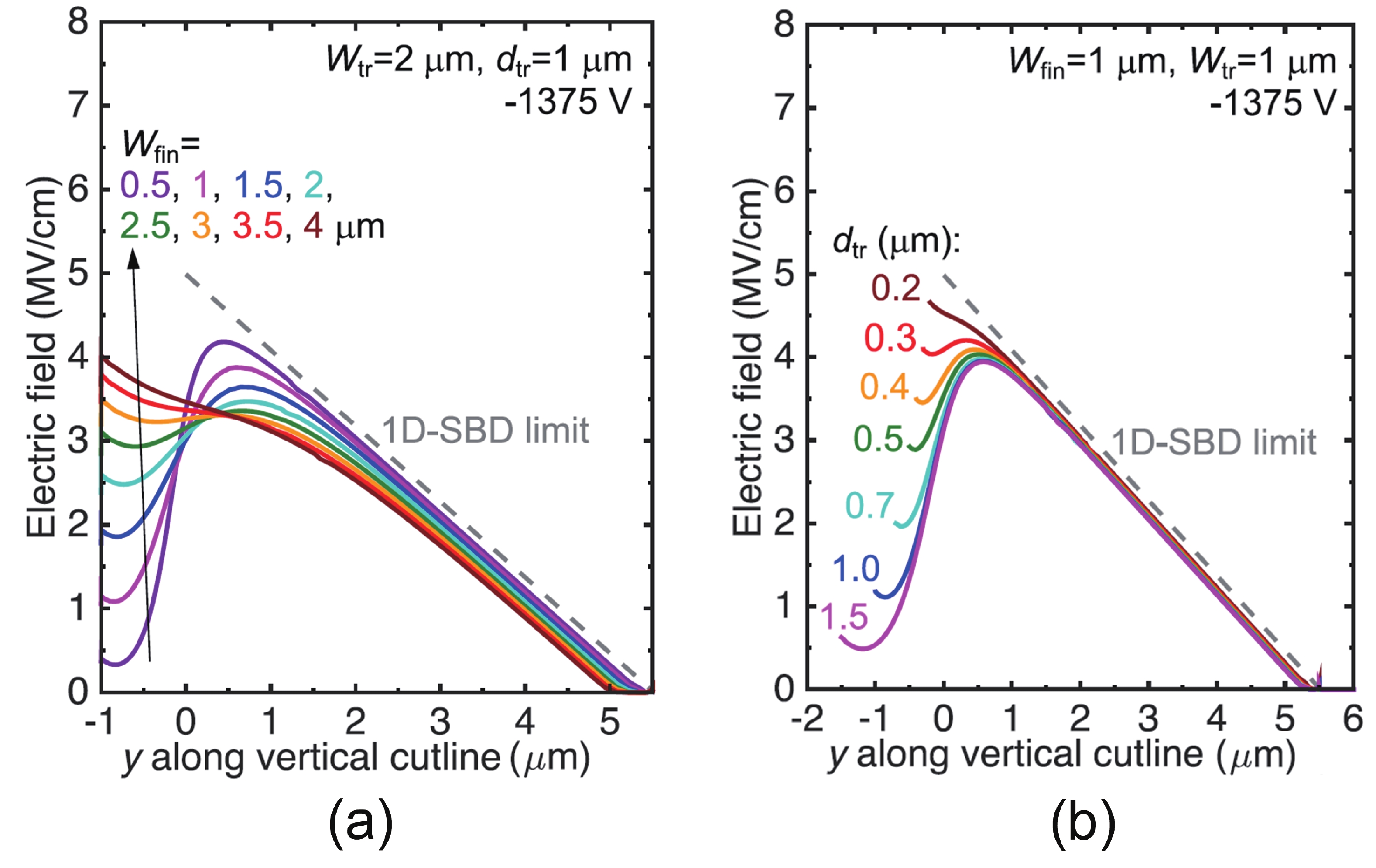
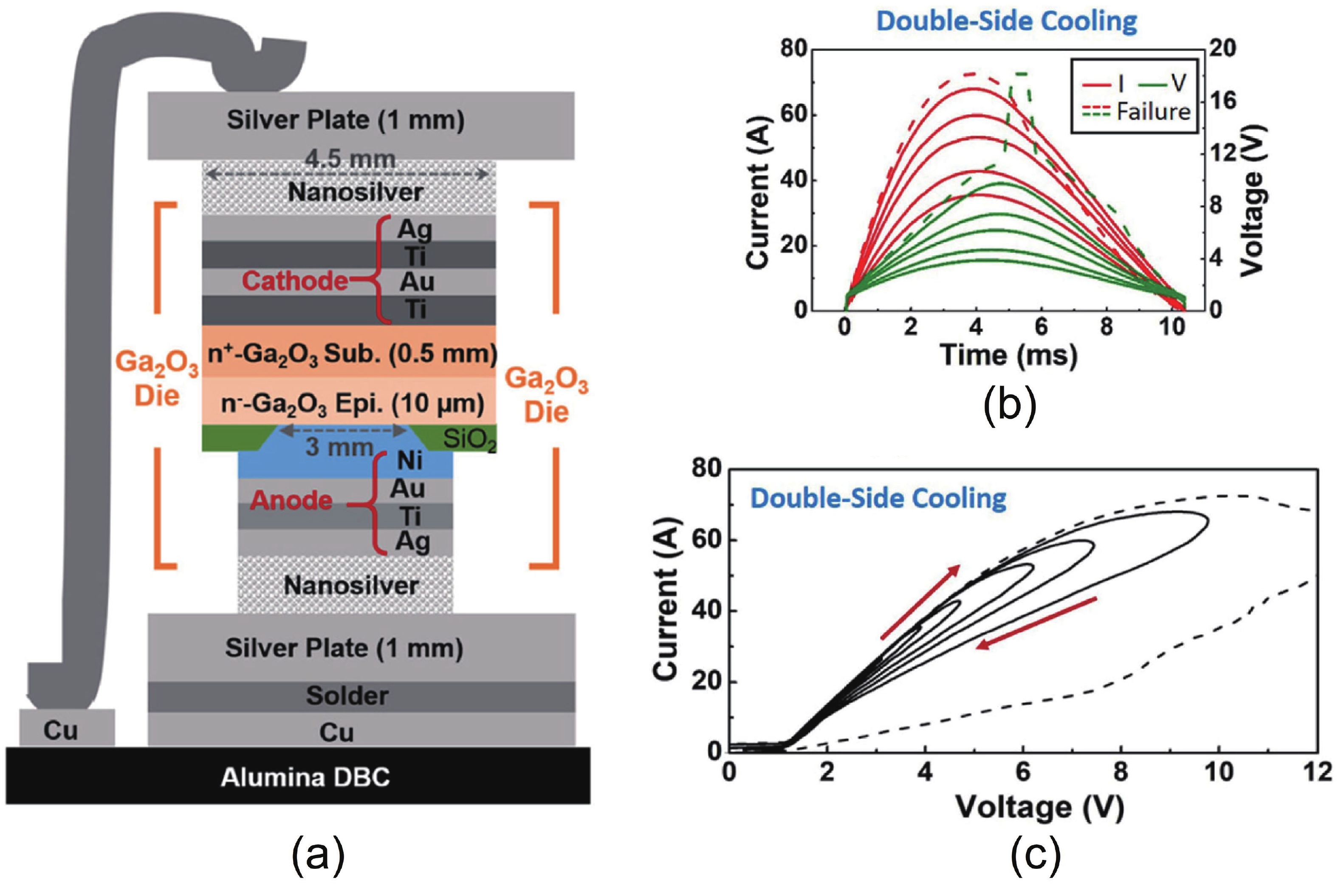
β-Ga2O3 Schottky barrier diodes have undergone rapid progress in research and development for power electronic applications. This paper reviews state-of-the-art β-Ga2O3 rectifier technologies, including advanced diode architectures that have enabled lower reverse leakage current via the reduced-surface-field effect. Characteristic device properties including on-resistance, breakdown voltage, rectification ratio, dynamic switching, and nonideal effects are summarized for the different devices. Notable results on the high-temperature resilience of β-Ga2O3 Schottky diodes, together with the enabling thermal packaging solutions, are also presented.


J. Semicond.
2023, 44(9): 092601 doi: 10.1088/1674-4926/44/9/092601
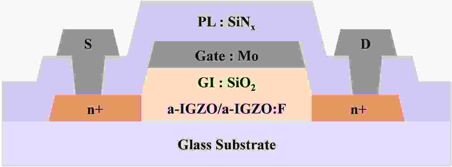
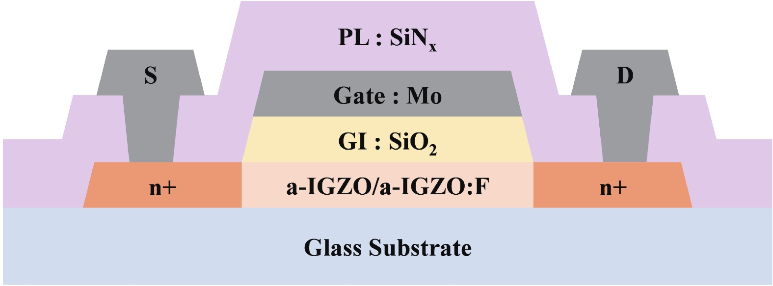
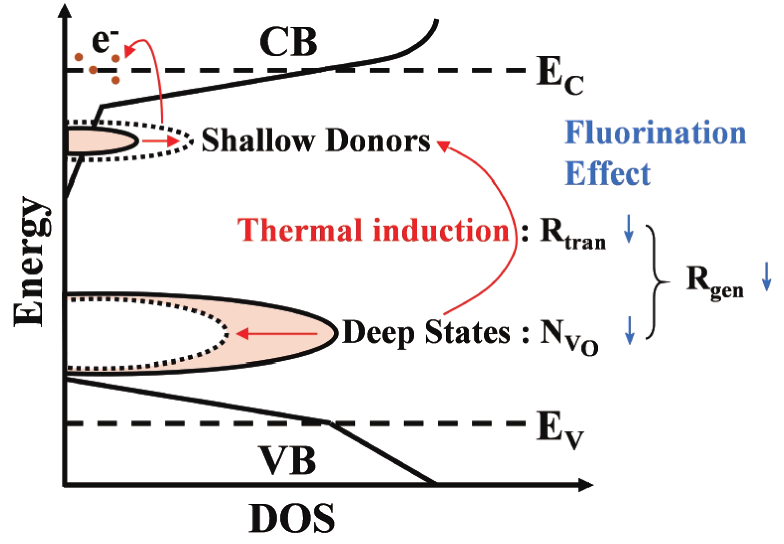
As growing applications demand higher driving currents of oxide semiconductor thin-film transistors (TFTs), severe instabilities and even hard breakdown under high-current stress (HCS) become critical challenges. In this work, the triggering voltage of HCS-induced self-heating (SH) degradation is defined in the output characteristics of amorphous indium-gallium-zinc oxide (a-IGZO) TFTs, and used to quantitatively evaluate the thermal generation process of channel donor defects. The fluorinated a-IGZO (a-IGZO:F) was adopted to effectively retard the triggering of the self-heating (SH) effect, and was supposed to originate from the less population of initial deep-state defects and a slower rate of thermal defect transition in a-IGZO:F. The proposed scheme noticeably enhances the high-current applications of oxide TFTs.


J. Semicond.
2023, 44(9): 092602 doi: 10.1088/1674-4926/44/9/092602
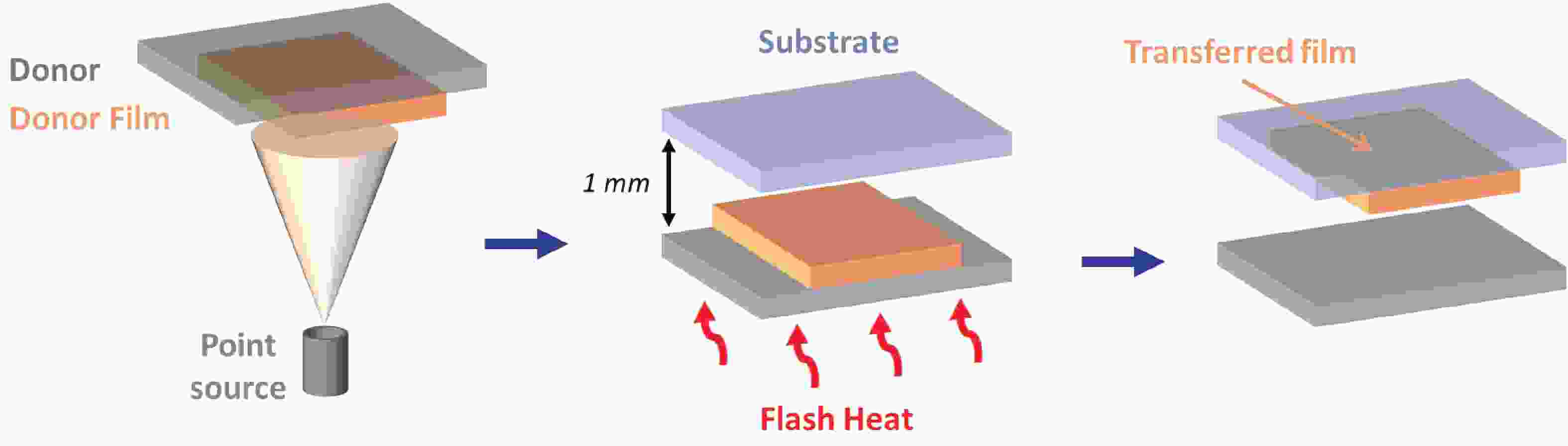
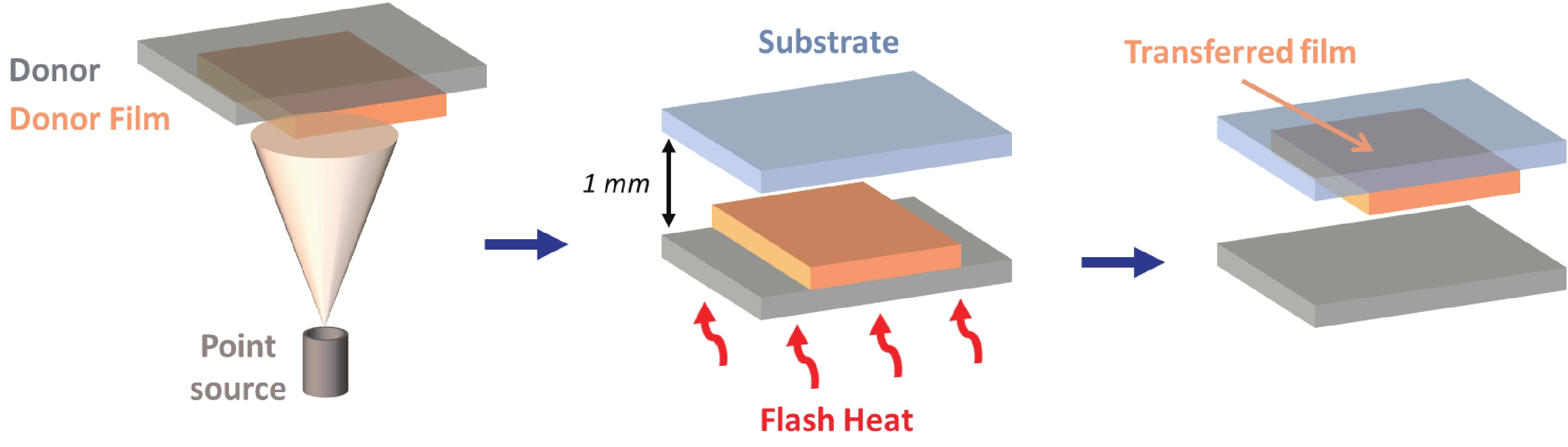
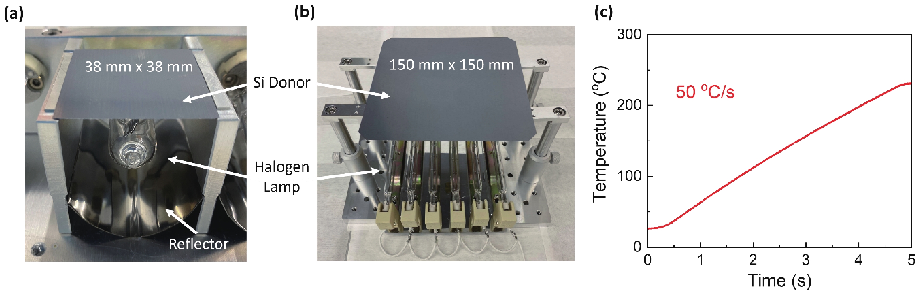
Close-space sublimation (CSS) has been demonstrated as an alternative vacuum deposition technique for fabricating organic light-emitting diodes (OLEDs). CSS utilizes a planar donor plate pre-coated with organic thin films as an area source to rapidly transfer the donor film to a device substrate at temperatures below 200 °C. CSS is also conformal and capable of depositing on odd-shaped substrates using flexible donor media. The evaporation behaviors of organic donor films under CSS were fully characterized using model OLED materials and CSS-deposited films exhibited comparable device performances in an OLED stack to films deposited by conventional point sources. The low temperature and conformal nature of CSS, along with its high material utilization and short process time, make it a promising method for fabricating flexible OLED displays.


J. Semicond.
2023, 44(9): 092603 doi: 10.1088/1674-4926/44/9/092603

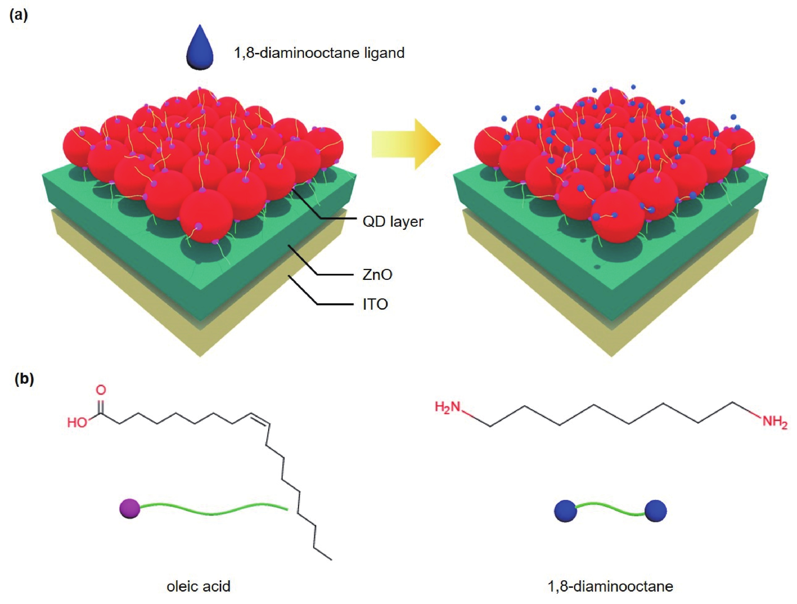
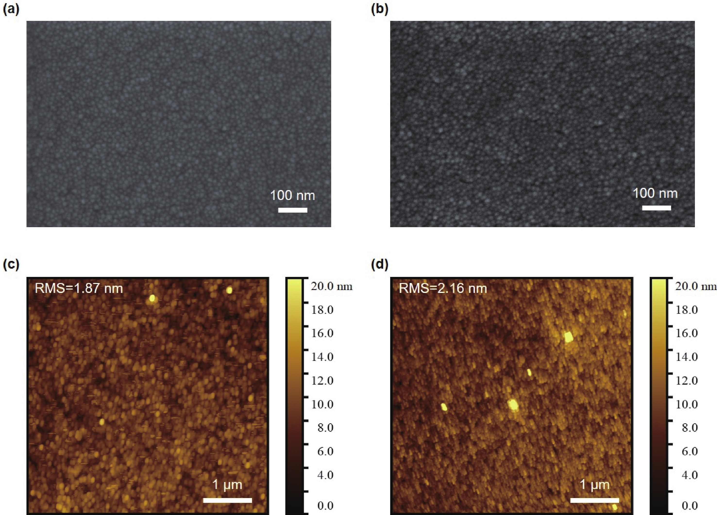
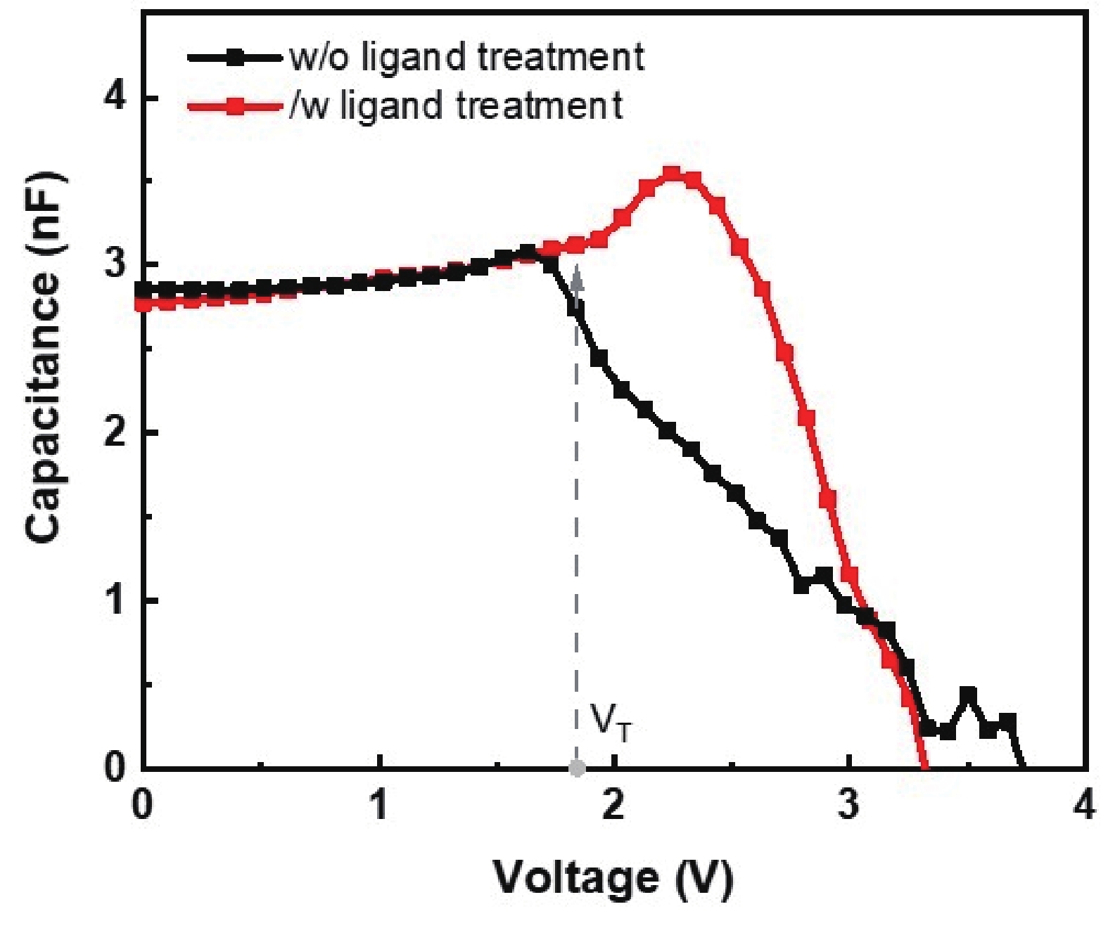
The performance of inverted quantum-dot light-emitting diodes (QLEDs) based on solution-processed hole transport layers (HTLs) has been limited by the solvent-induced damage to the quantum dot (QD) layer during the spin-coating of the HTL. The lack of compatibility between the HTL's solvent and the QD layer results in an uneven surface, which negatively impacts the overall device performance. In this work, we develop a novel method to solve this problem by modifying the QD film with 1,8-diaminooctane to improve the resistance of the QD layer for the HTL’s solvent. The uniform QD layer leads the inverted red QLED device to achieve a low turn-on voltage of 1.8 V, a high maximum luminance of 105 500 cd/m2, and a remarkable maximum external quantum efficiency of 13.34%. This approach releases the considerable potential of HTL materials selection and offers a promising avenue for the development of high-performance inverted QLEDs.


J. Semicond.
2023, 44(9): 092604 doi: 10.1088/1674-4926/44/9/092604

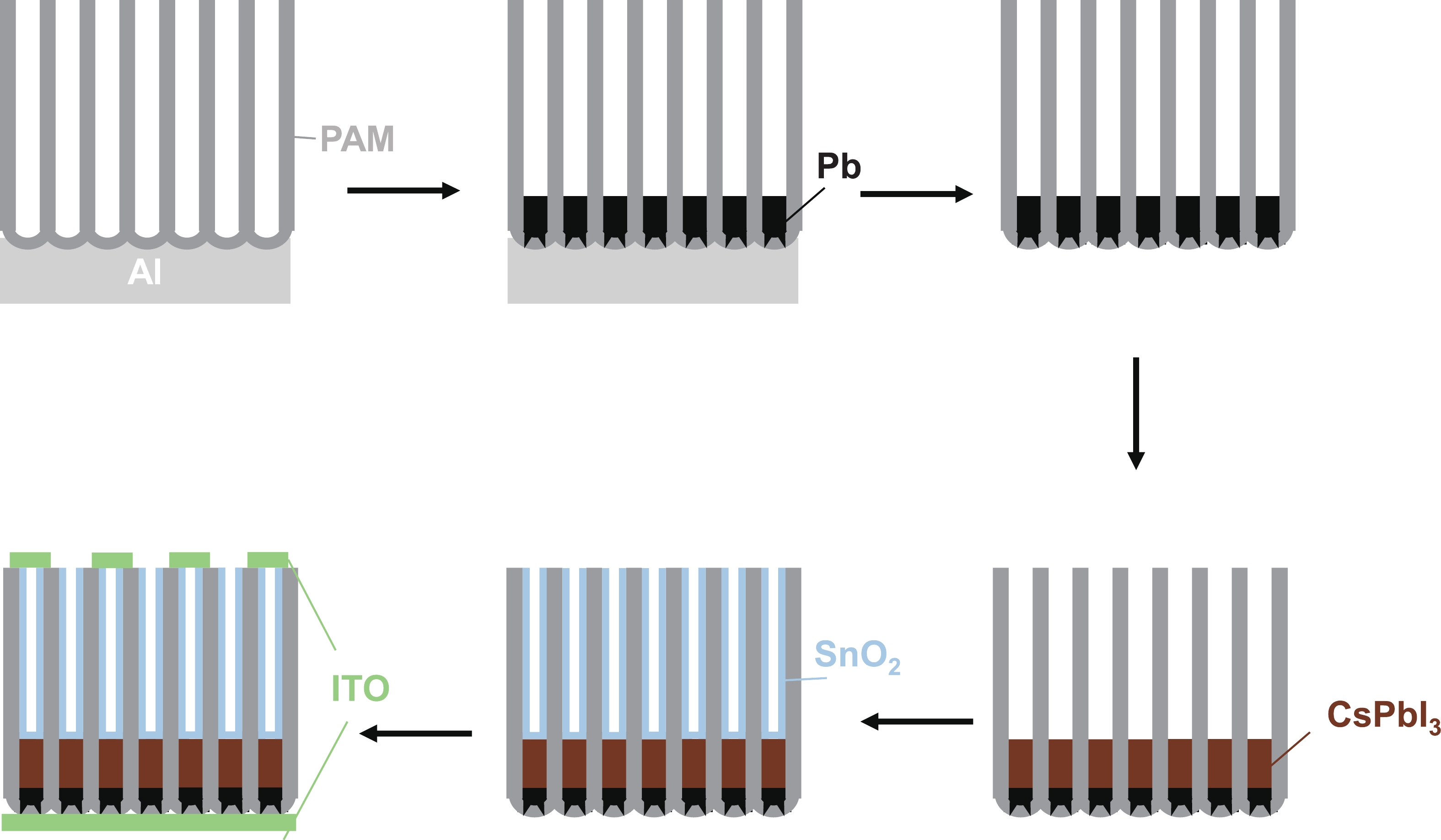
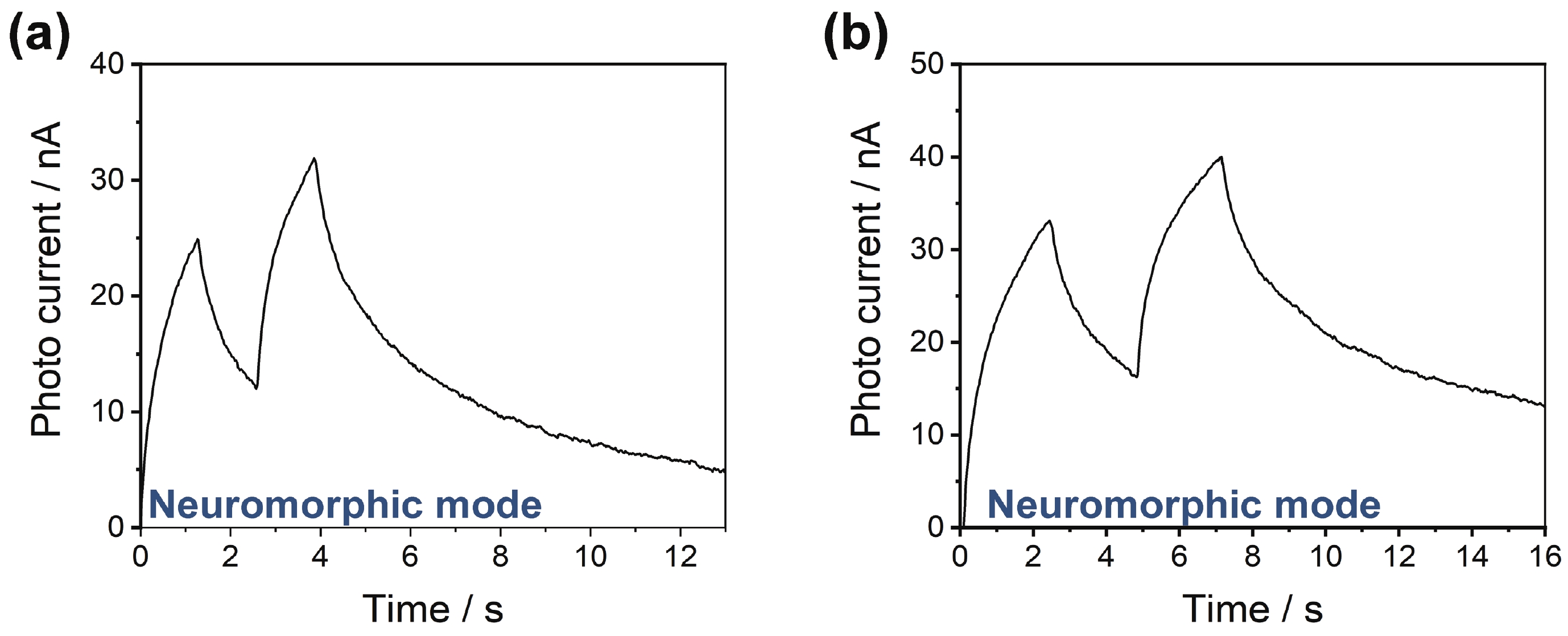
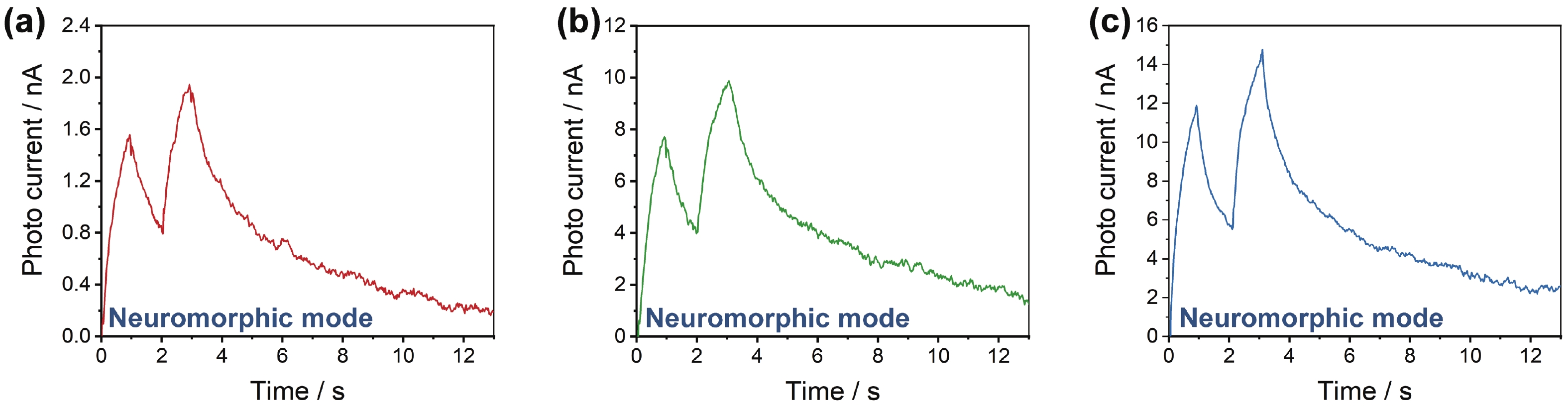
The high-density, vertically aligned retinal neuron array provides effective vision, a feature we aim to replicate with electronic devices. However, the conventional complementary metal-oxide-semiconductor (CMOS) image sensor, based on separate designs for sensing, memory, and processing units, limits its integration density. Moreover, redundant signal communication significantly increases energy consumption. Current neuromorphic devices integrating sensing and signal processing show promise in various computer vision applications, but there is still a need for frame-based imaging with good compatibility. In this study, we developed a dual-mode image sensor based on a high-density all-inorganic perovskite nanowire array. The device can switch between frame-based standard imaging mode and neuromorphic imaging mode by applying different biases. This unique bias-dependent photo response is based on a well-designed energy band diagram. The biomimetic alignment of nanowires ensures the potential for high-resolution imaging. To further demonstrate the imaging ability, we conducted pattern reconstruction in both modes with a 10 × 10 crossbar device. This study introduces a novel image sensor with high compatibility and efficiency, suitable for various applications including computer vision, surveillance, and robotics.


J. Semicond.
2023, 44(9): 092605 doi: 10.1088/1674-4926/44/9/092605
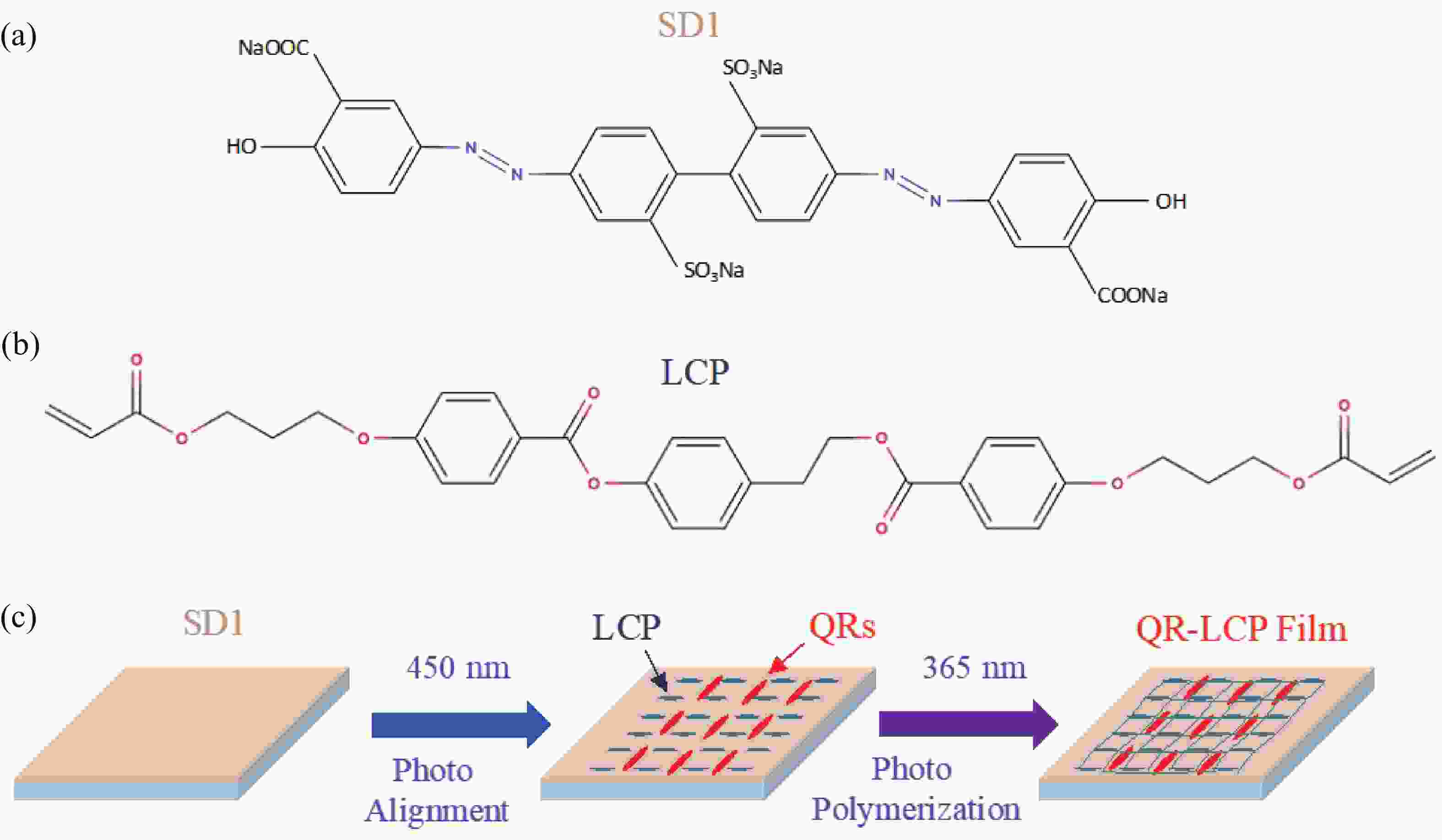
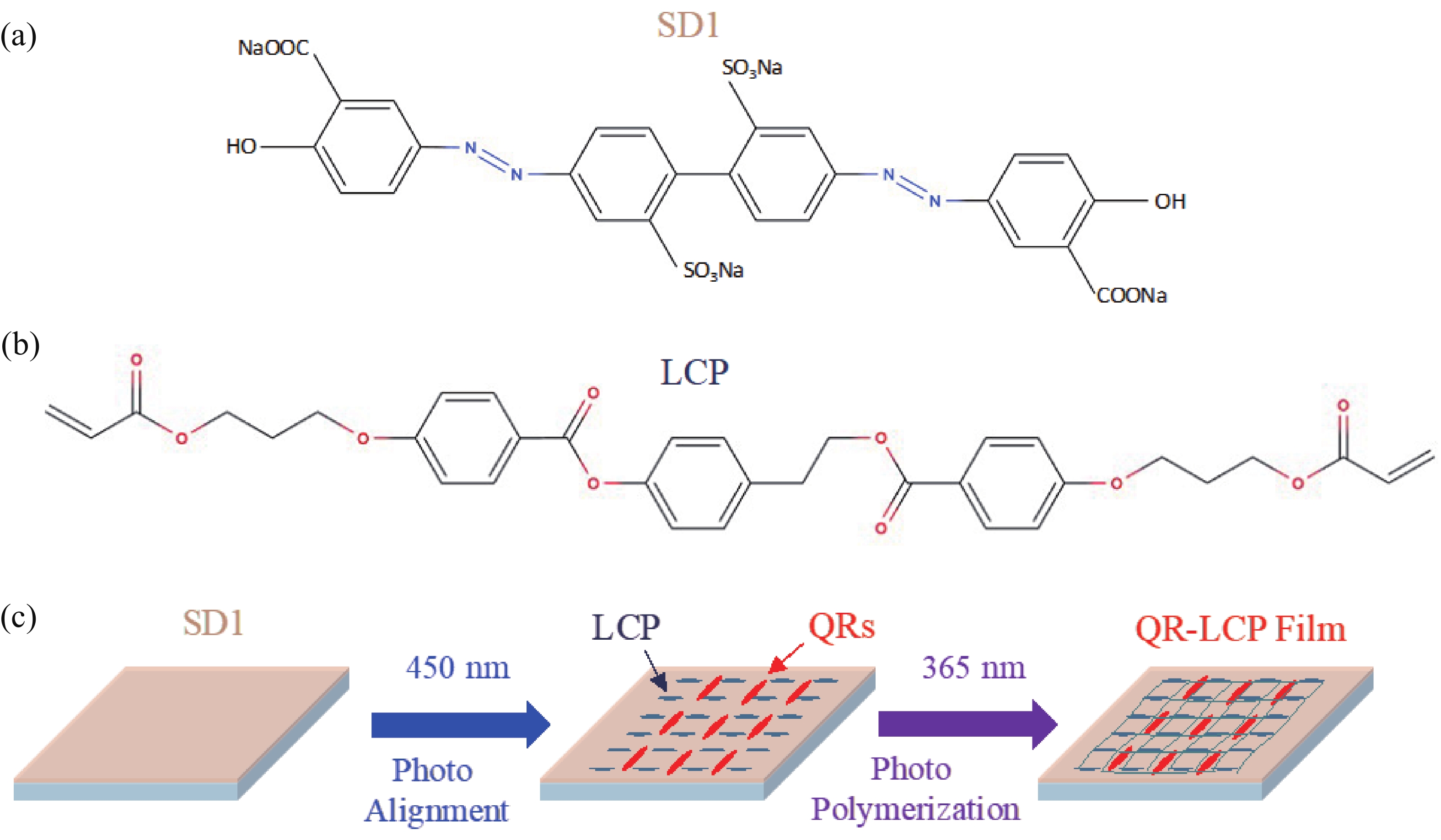
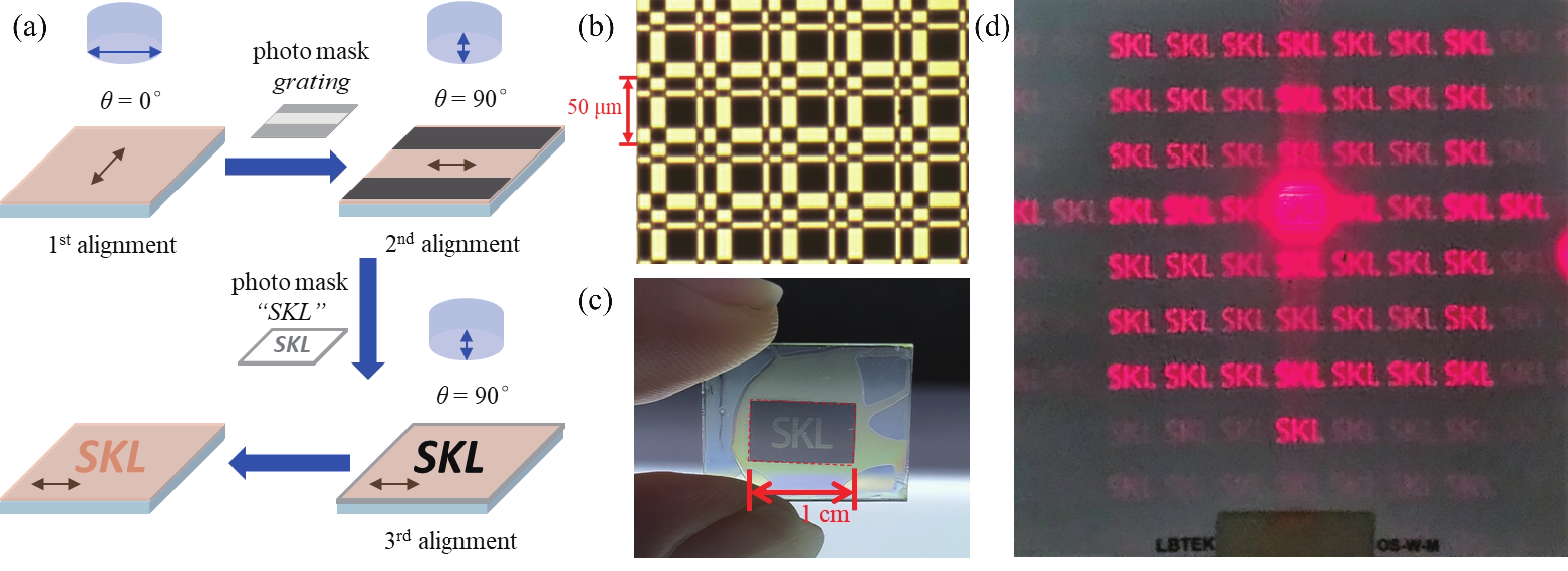
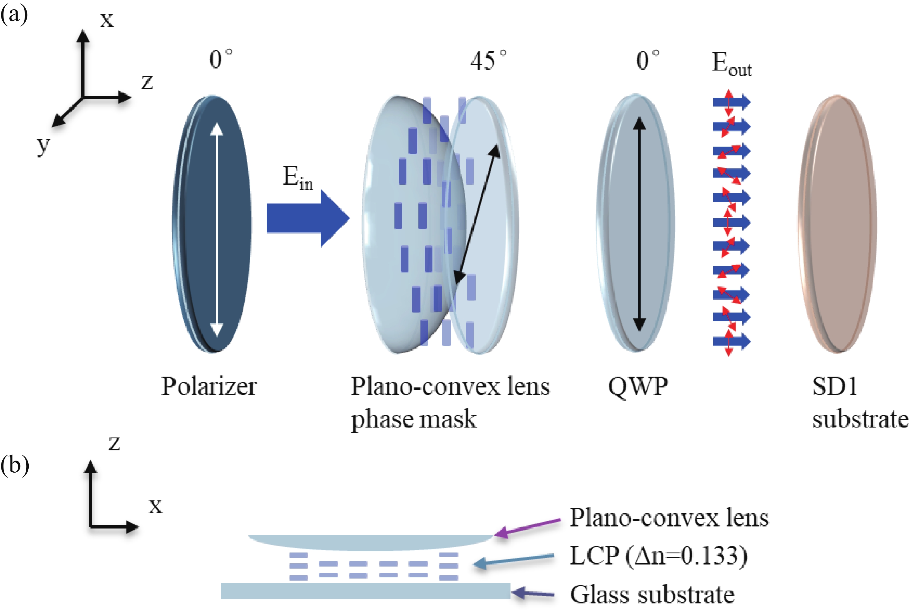
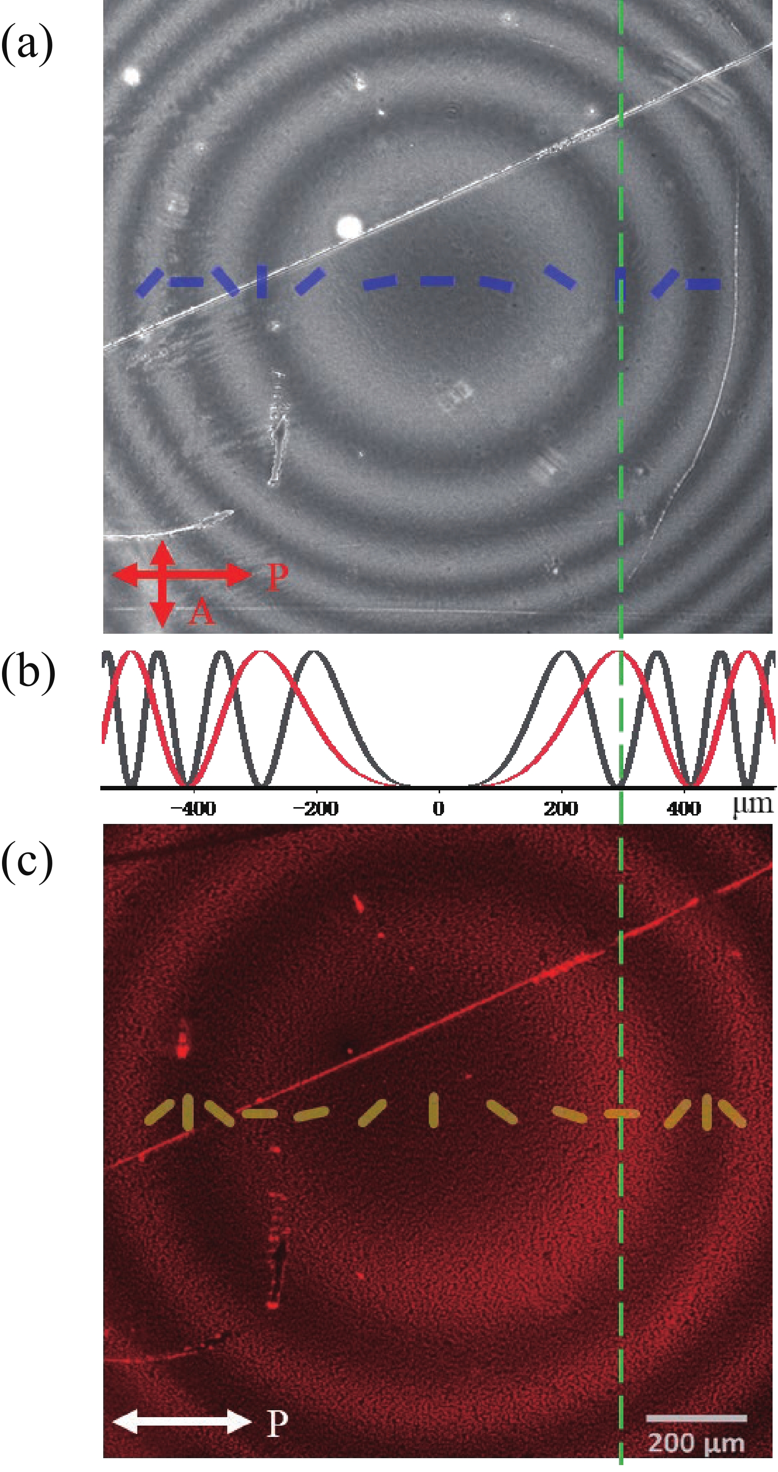
The anisotropic absorption and emission from semiconductor CdSe/CdS quantum rods (QRs) provide extra benefits among other photoluminescence nanocrystals. Using photo-induced alignment technique, the QRs can be oriented in liquid crystal polymer matrix at a large scale. In this article, a 2D Dammann grating pattern, within “SKL” characters domains aligned QRs in composite film, was fabricated by multi-step photo exposure using several photo masks, and a continuous geometric lens profile pattern aligned QRs was realized by the single step polarization converting holographic irradiation method. Both polarized optical microscope and fluorescence microscope are employed to determine the liquid crystal director profiles and QRs anisotropic excitation properties. We have been able to orient the QRs in fine binary and continuous patterns that confirms the strong quantum rod aligning ability of the proposed method. Thus, the proposed approach paves a way for photo-induced flexible QRs alignments to provide a highly specific and difficult-to-replicate security application at a large scale.