


Issue Browser
Volume 42, Issue 11,
Nov 2021
Column

J. Semicond.
2021, 42(11): 112001 doi: 10.1088/1674-4926/42/11/112001
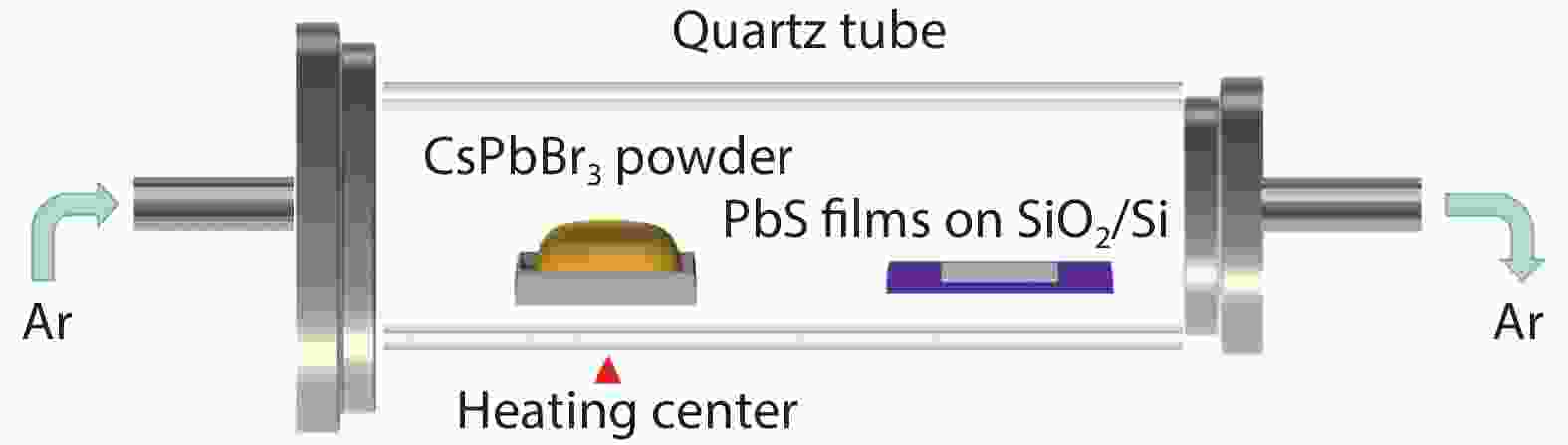
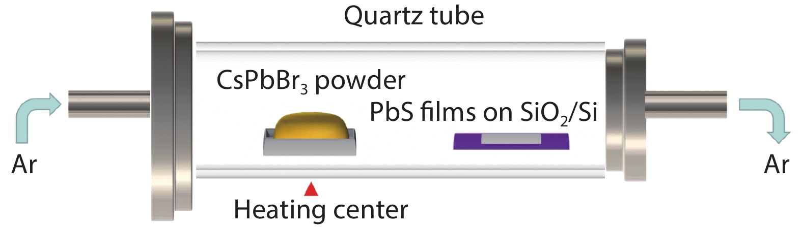
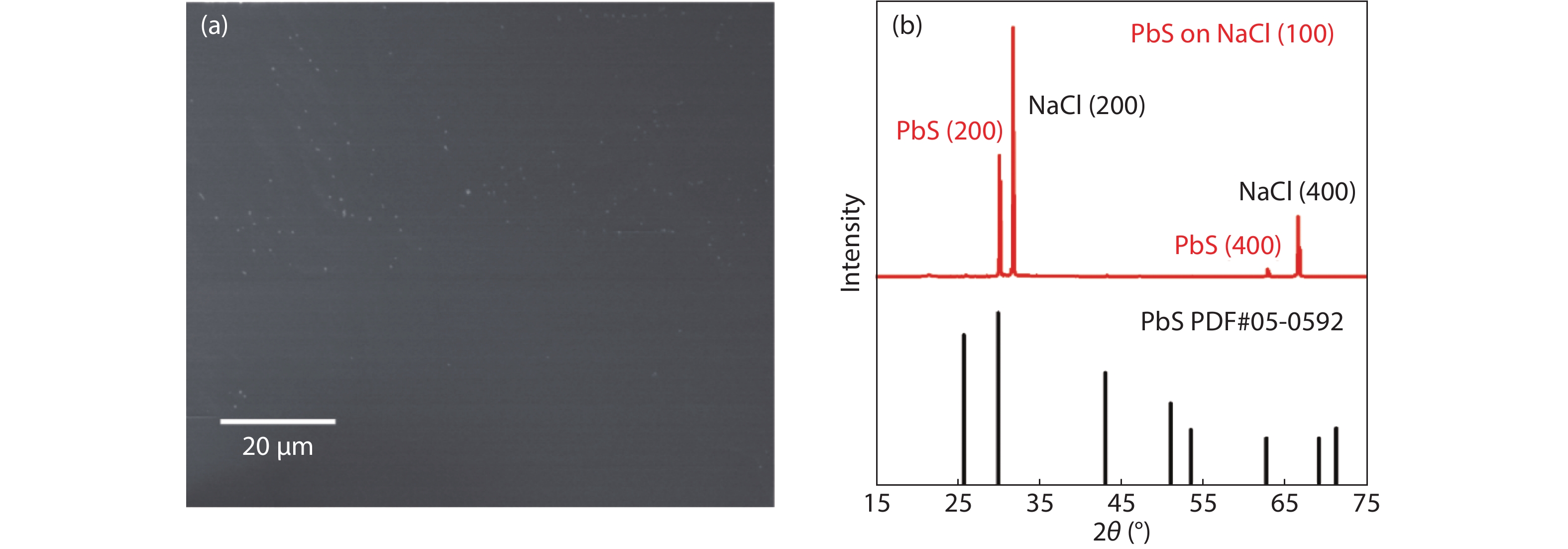
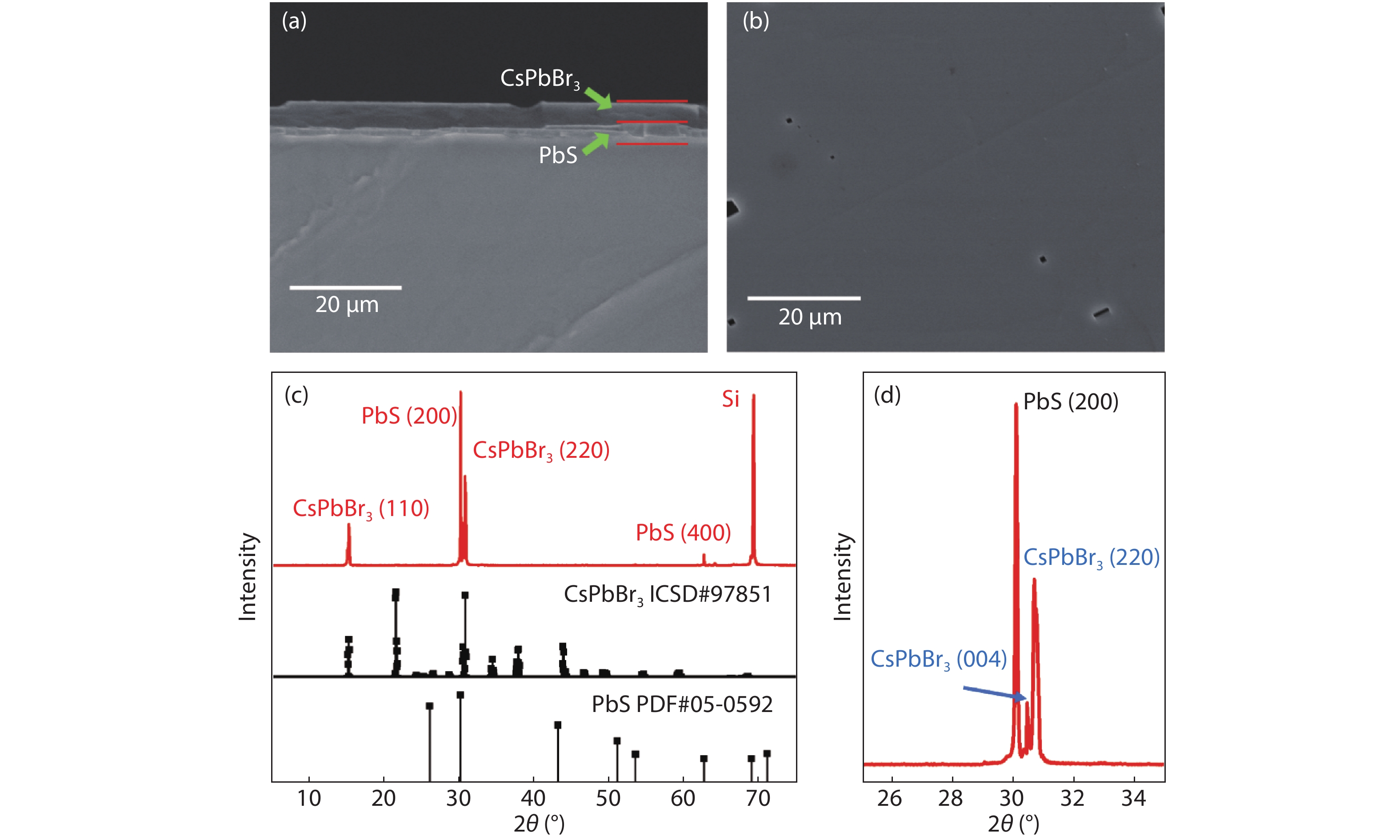
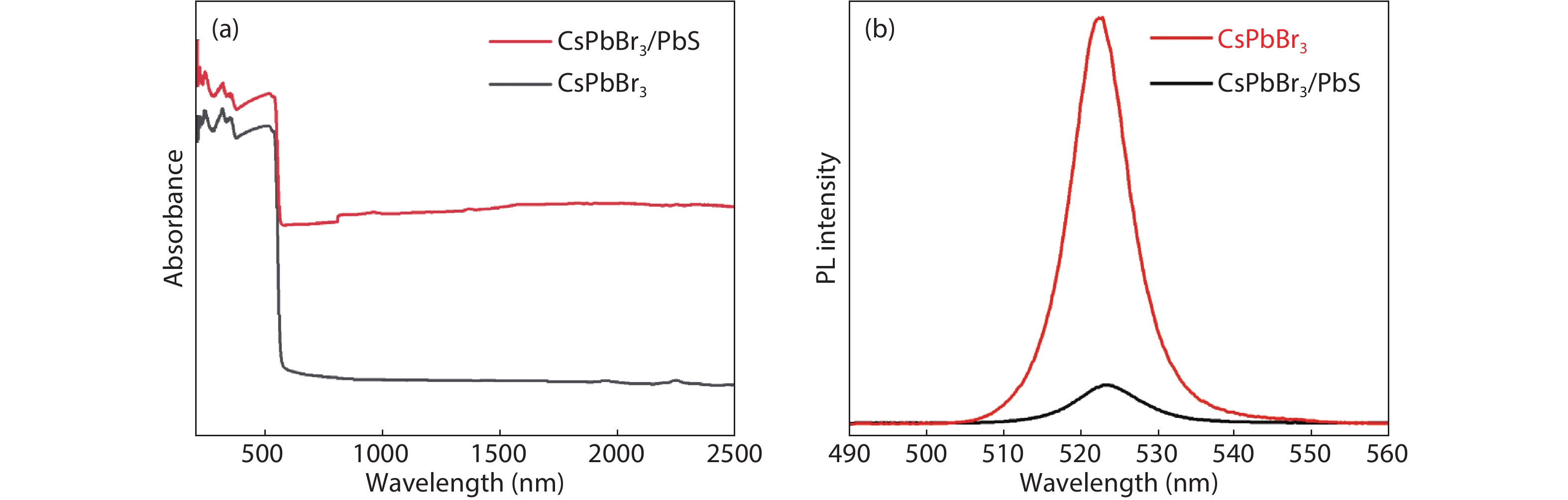
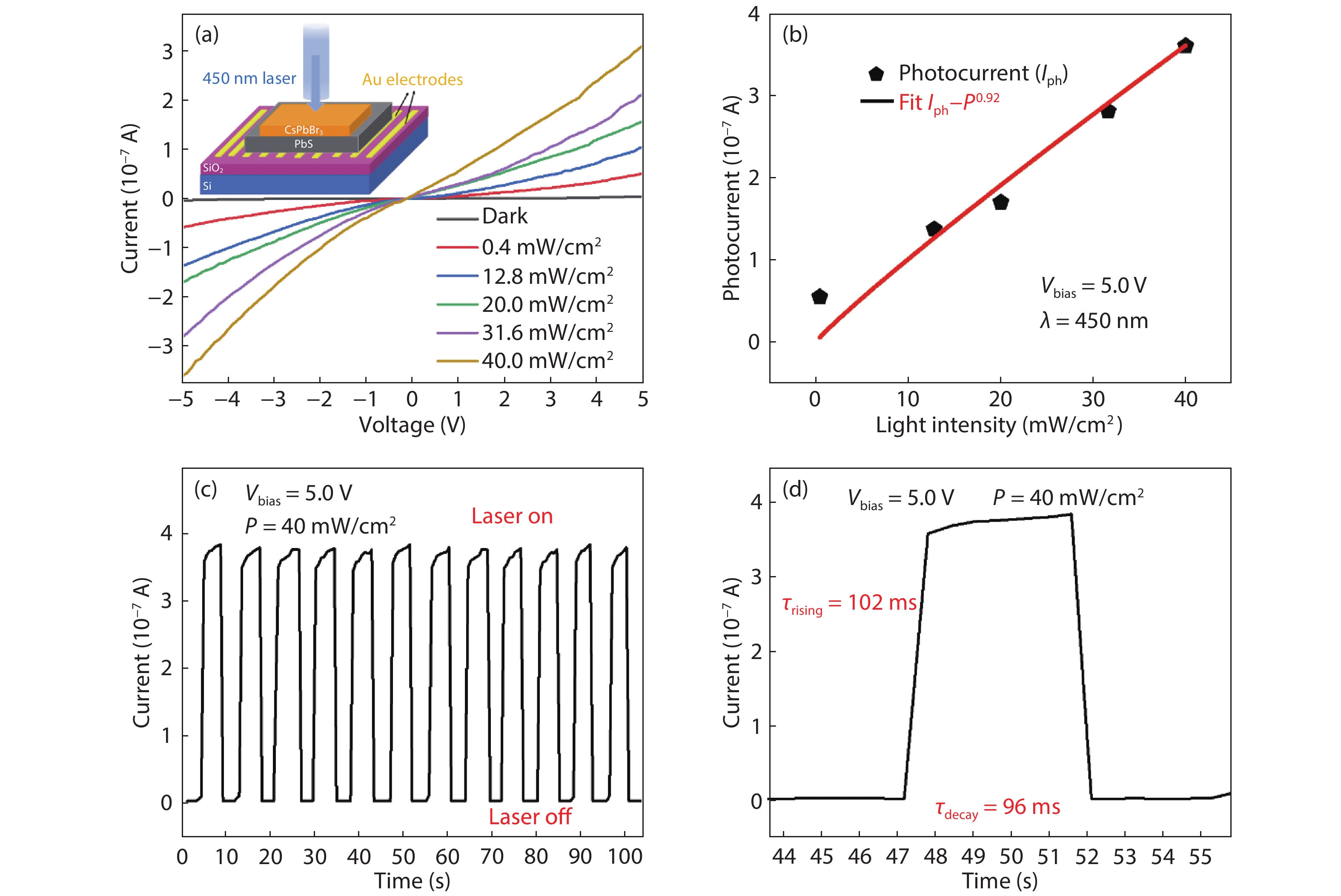
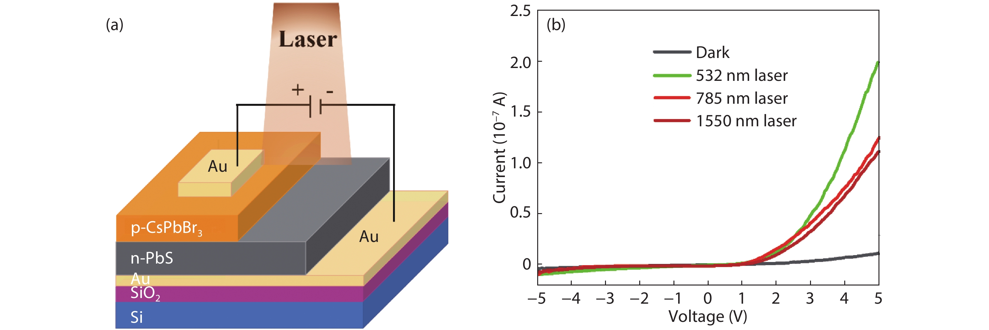
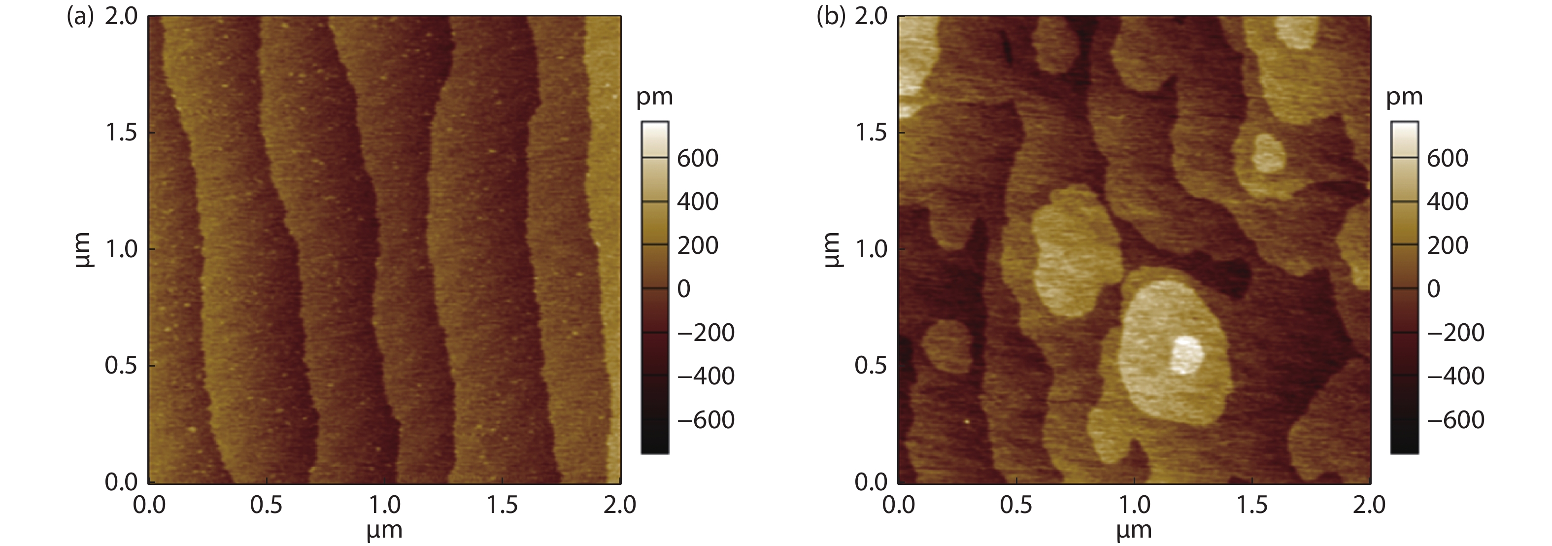
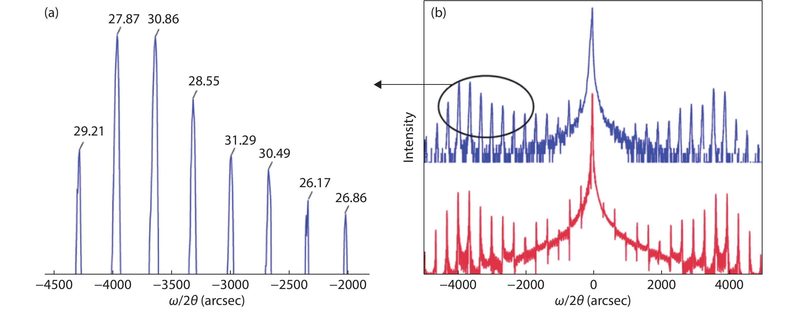
Epitaxial high-crystallization film semiconductor heterostructures has been proved to be an effective method to prepare single-crystal films for different functional devices in modern microelectronics, electro-optics, and optoelectronics. With superior semiconducting properties, halide perovskite materials are rising as building blocks for heterostructures. Here, the conformal vapor phase epitaxy of CsPbBr3 on PbS single-crystal films is realized to form the CsPbBr3/PbS heterostructures via a two-step vapor deposition process. The structural characterization reveals that PbS substrates and the epilayer CsPbBr3 have clear relationships: CsPbBr3(110) // PbS(100), CsPbBr3[


J. Semicond.
2021, 42(11): 112002 doi: 10.1088/1674-4926/42/11/112002
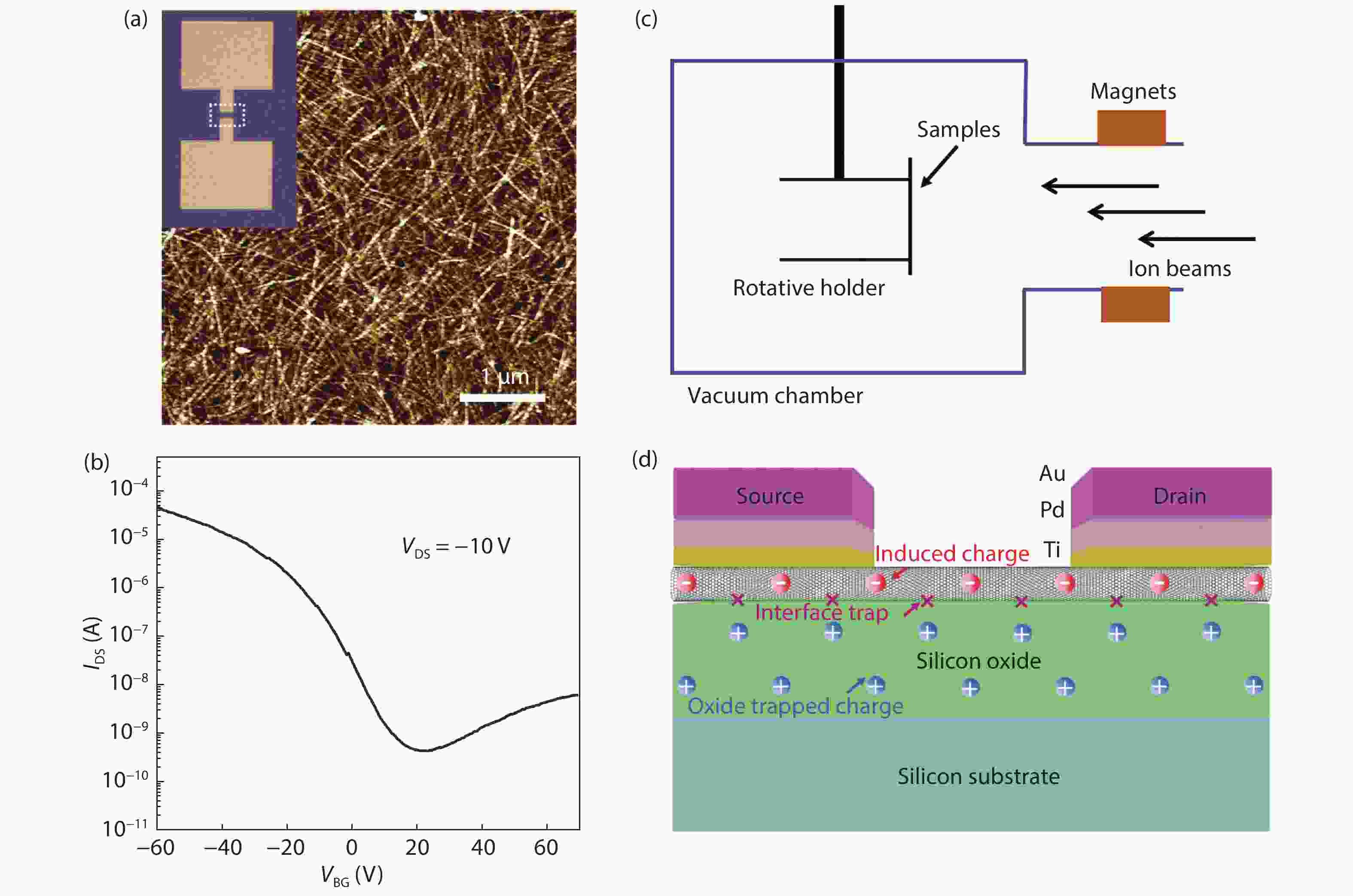
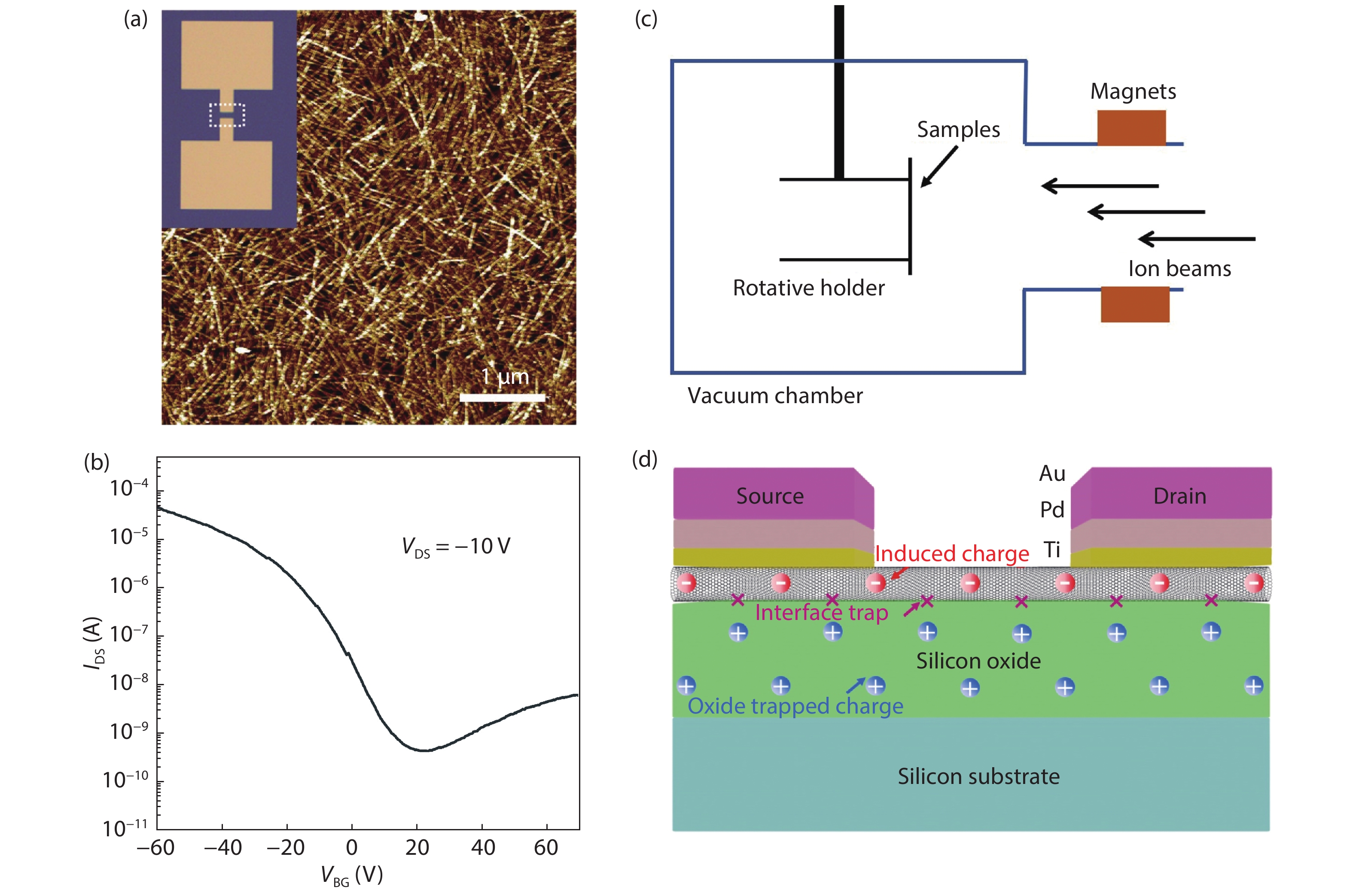
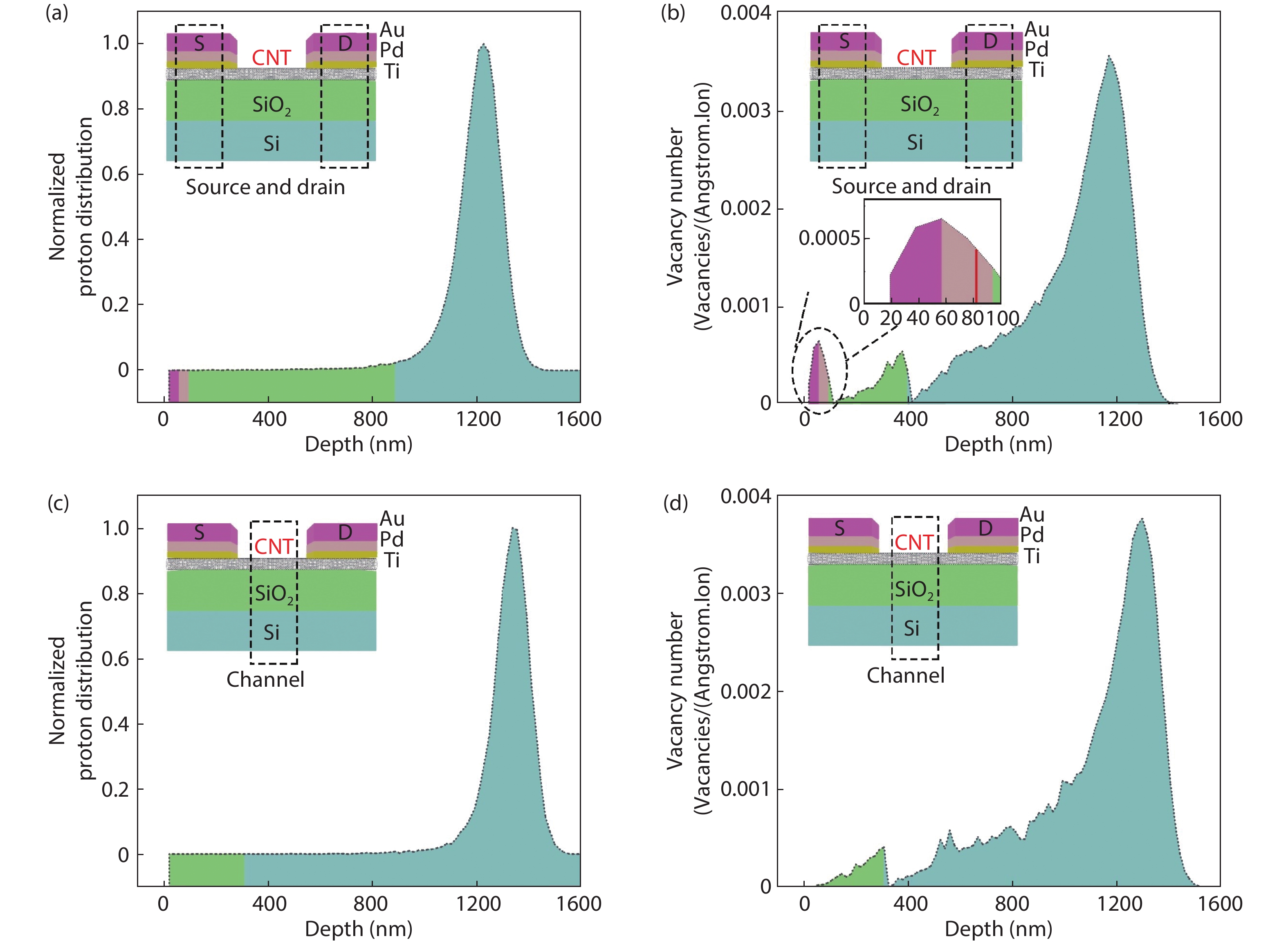
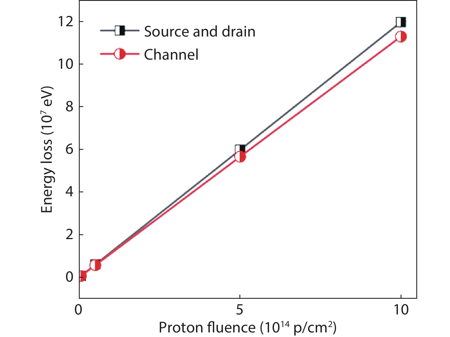
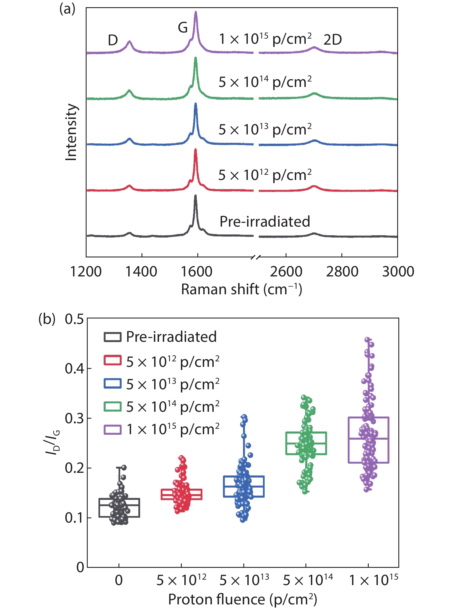
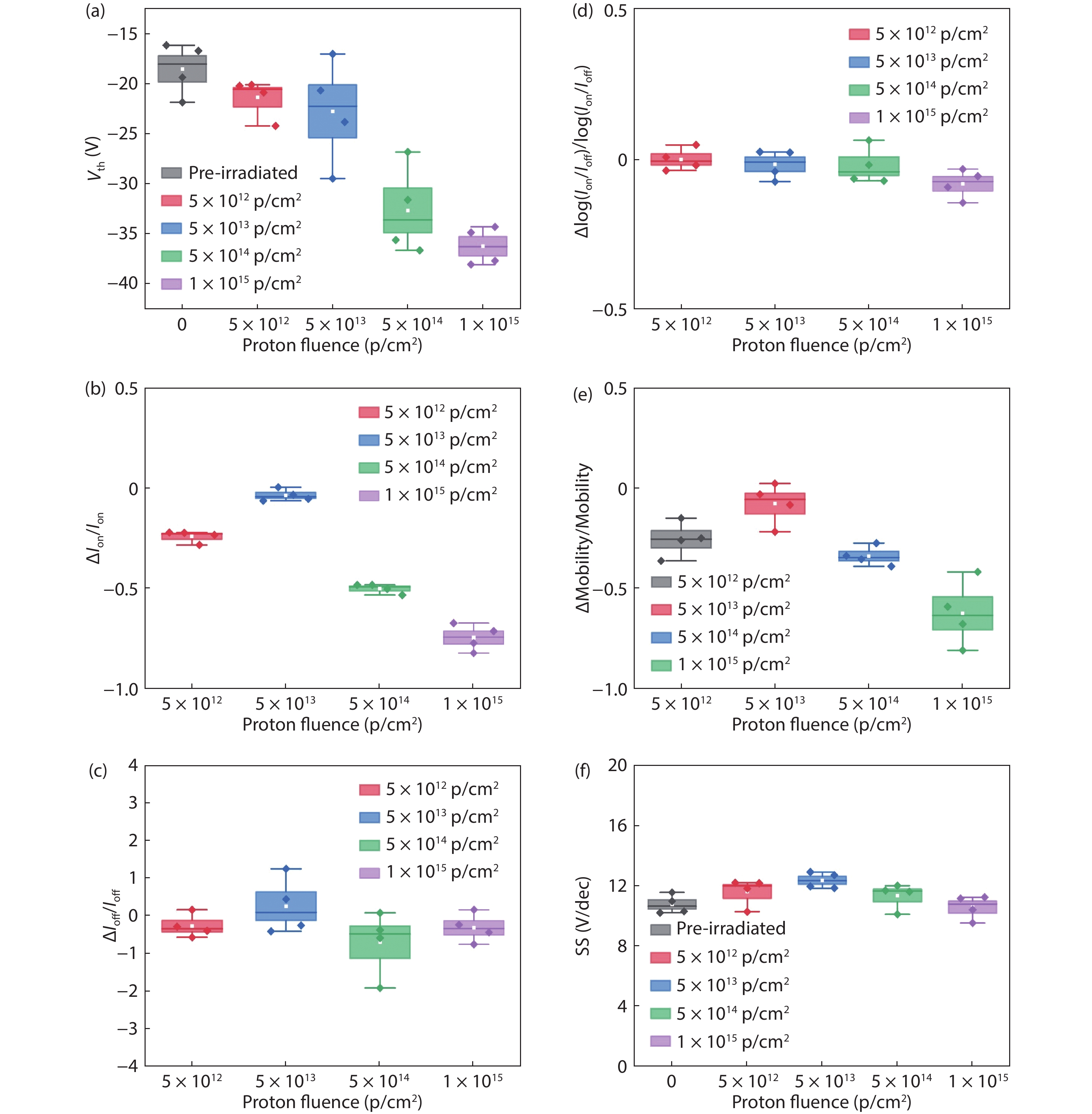
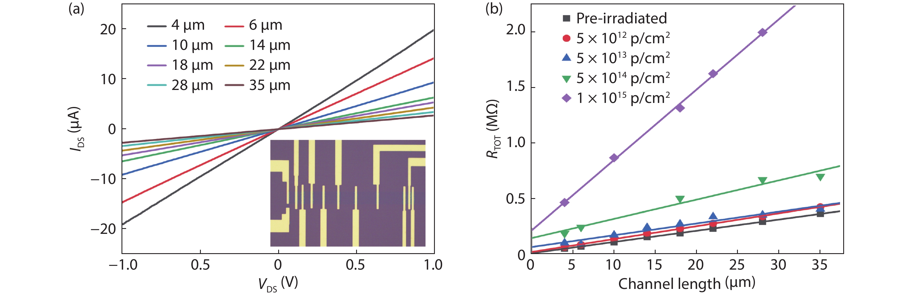
Strong C–C bonds, nanoscale cross-section and low atomic number make single-walled carbon nanotubes (SWCNTs) a potential candidate material for integrated circuits (ICs) applied in outer space. However, very little work combines the simulation calculations with the electrical measurements of SWCNT field-effect transistors (FETs), which limits further understanding on the mechanisms of radiation effects. Here, SWCNT film-based FETs were fabricated to explore the total ionizing dose (TID) and displacement damage effect on the electrical performance under low-energy proton irradiation with different fluences up to 1 × 10¹⁵ p/cm2. Large negative shift of the threshold voltage and obvious decrease of the on-state current verified the TID effect caused in the oxide layer. The stability of the subthreshold swing and the off-state current reveals that the displacement damage caused in the CNT layer is not serious, which proves that the CNT film is radiation-hardened. Specially, according to the simulation, we found the displacement damage caused by protons is different in the source/drain contact area and channel area, leading to varying degrees of change for the contact resistance and sheet resistance. Having analyzed the simulation results and electrical measurements, we explained the low-energy proton irradiation mechanism of the CNT FETs, which is essential for the construction of radiation-hardened CNT film-based ICs for aircrafts.

J. Semicond.
2021, 42(11): 112101 doi: 10.1088/1674-4926/42/11/112101
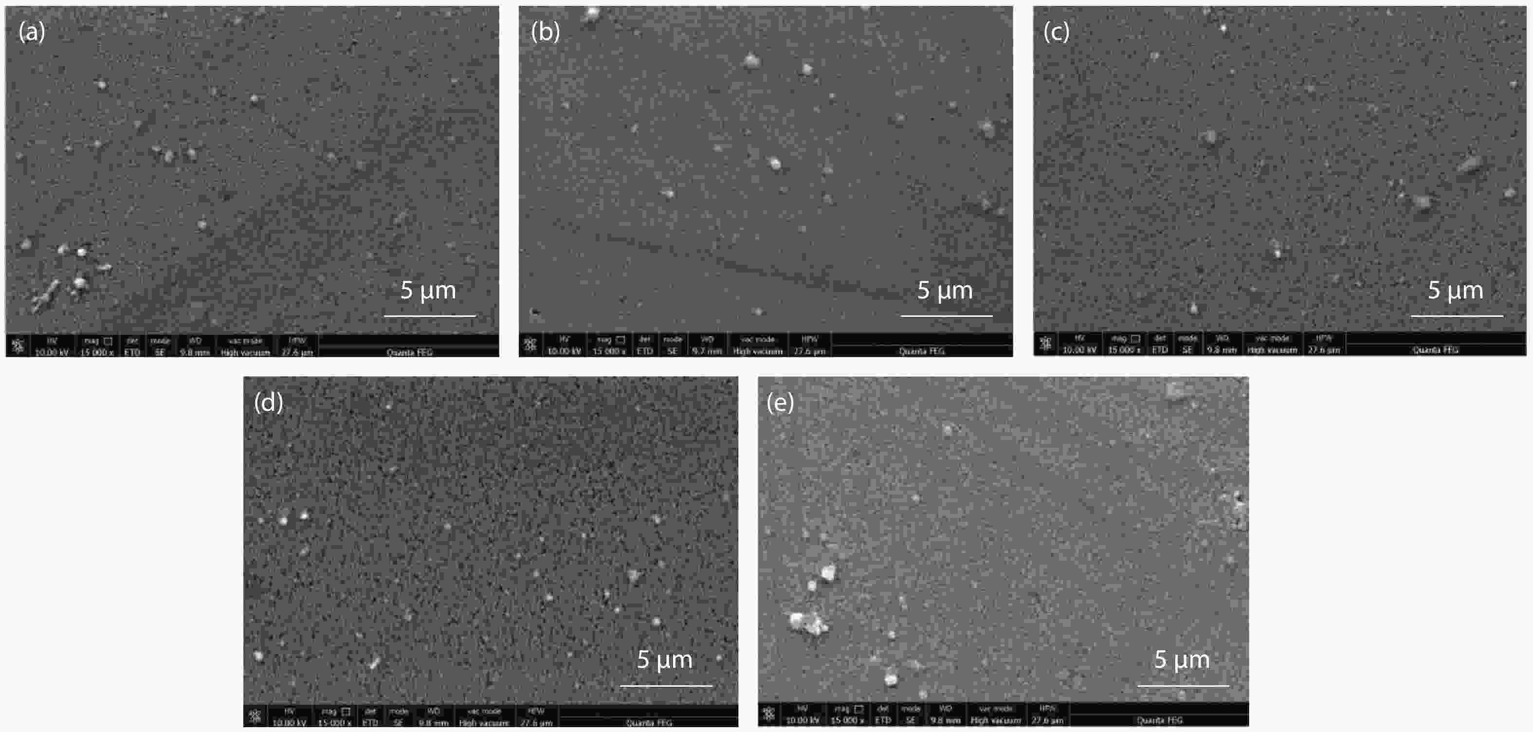
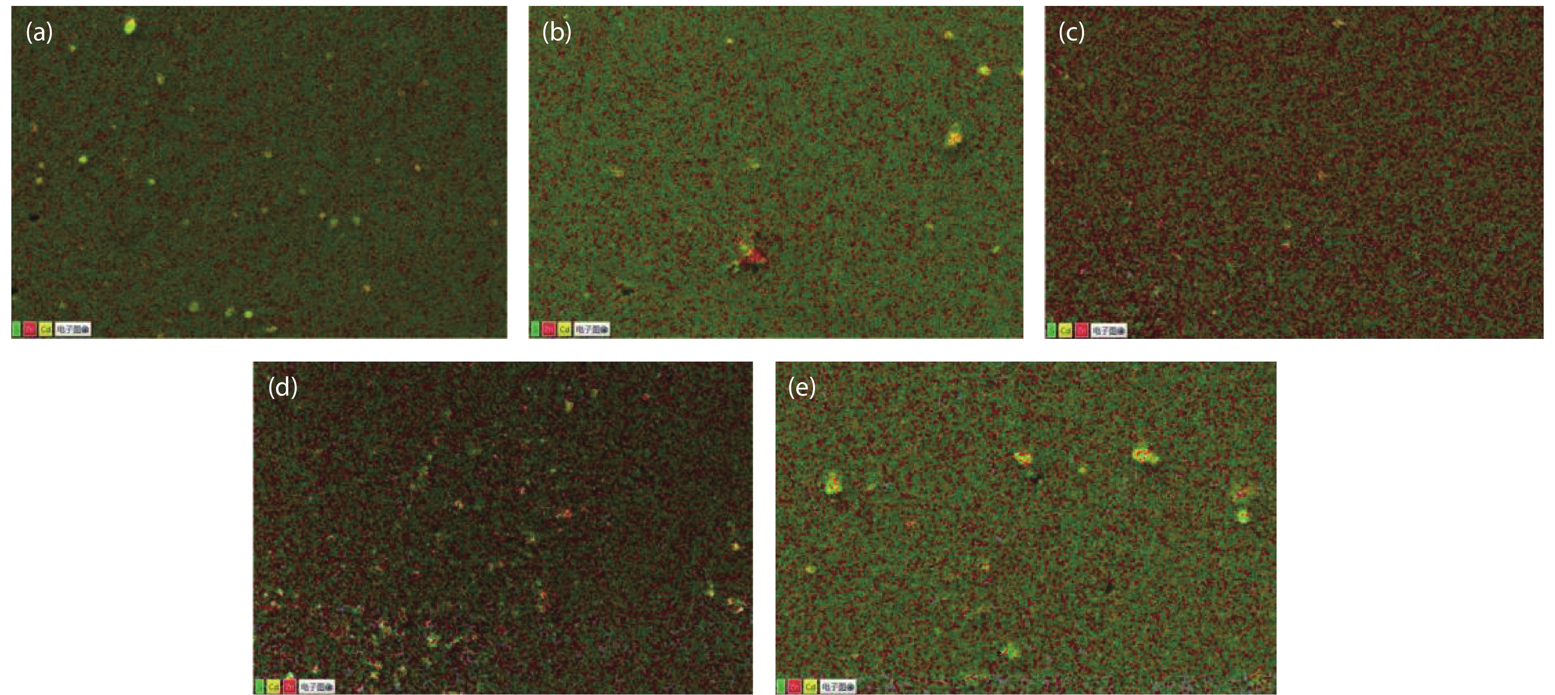
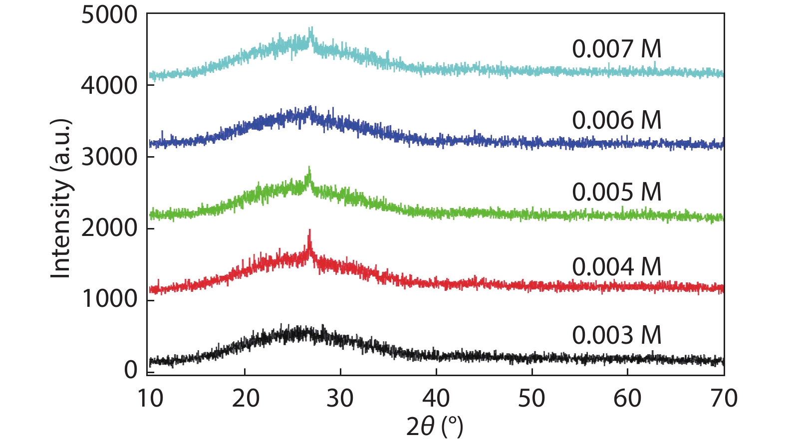
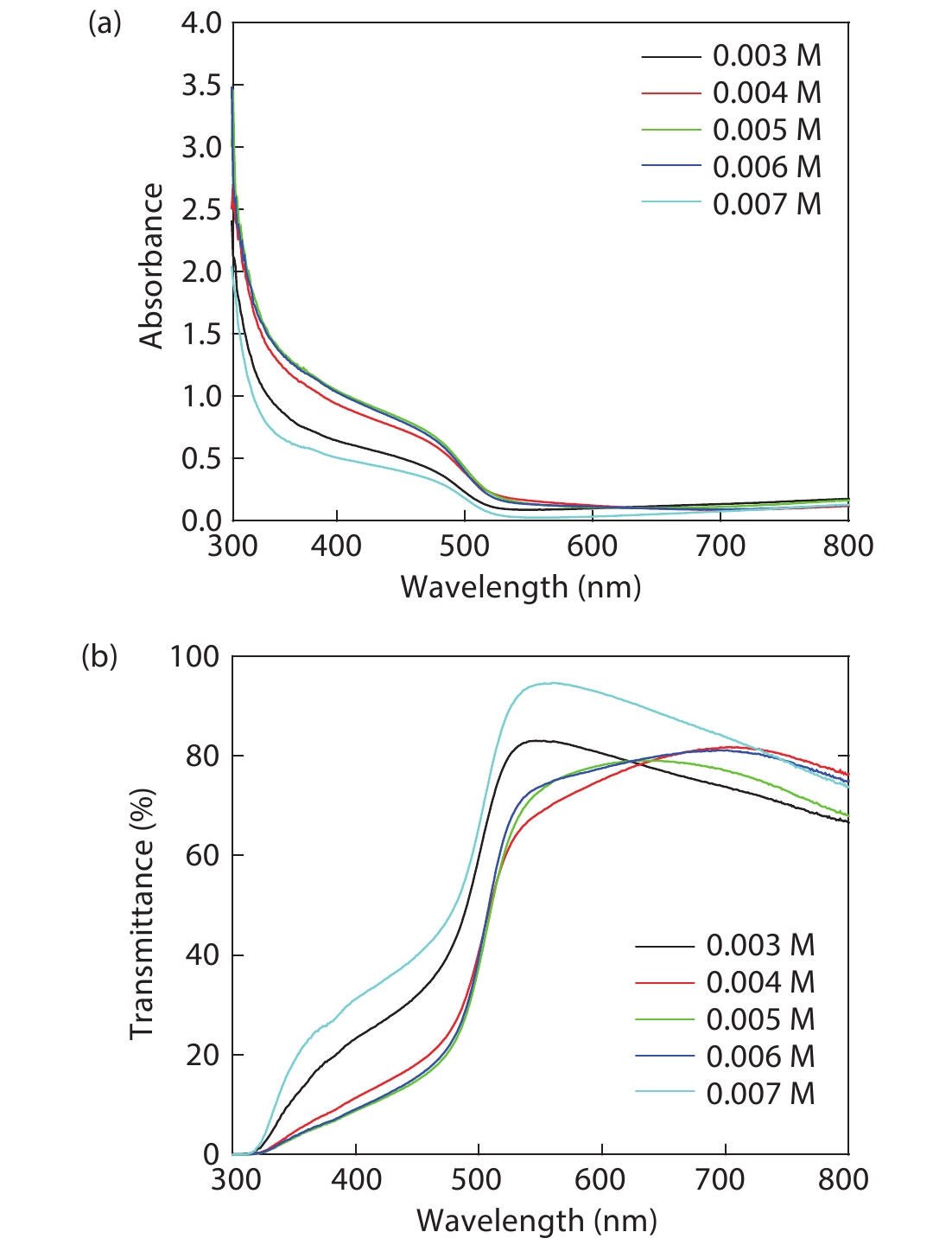
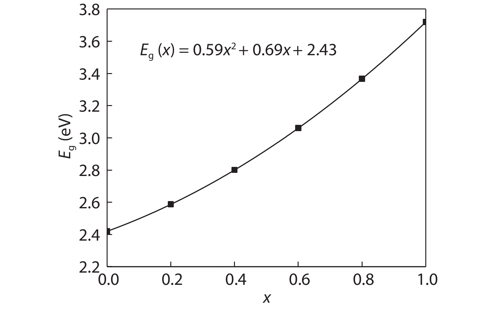
Cd1–xZnxS thin films were deposited by chemical bath deposition (CBD) on the glass substrate to study the influence of cadmium sulfate concentration on the structural characteristics of the thin film. The SEM results show that the thin film surfaces under the cadmium sulfate concentration of 0.005 M exhibit better compactness and uniformity. The distribution diagrams of thin film elements illustrate the film growth rate changes on the trend of the increase, decrease, and increase with the increase of cadmium sulfate concentration. XRD studies exhibit the crystal structure of the film is the hexagonal phase, and there are obvious diffraction peaks and better crystallinity when the concentration is 0.005 M. Spectrophotometer test results demonstrate that the relationship between zinc content x and optical band gap value Eg can be expressed by the equation Eg(x) = 0.59x2 + 0.69x + 2.43. Increasing the zinc content can increase the optical band gap, and the absorbance of the thin film can be improved by decreasing the cadmium sulfate concentration, however, all of them have good transmittance. At a concentration of 0.005 M, the thin film has good absorbance in the 300–800 nm range, 80% transmittance, and band gap value of 3.24 eV, which is suitable for use as a buffer layer for solar cells.


J. Semicond.
2021, 42(11): 112102 doi: 10.1088/1674-4926/42/11/112102

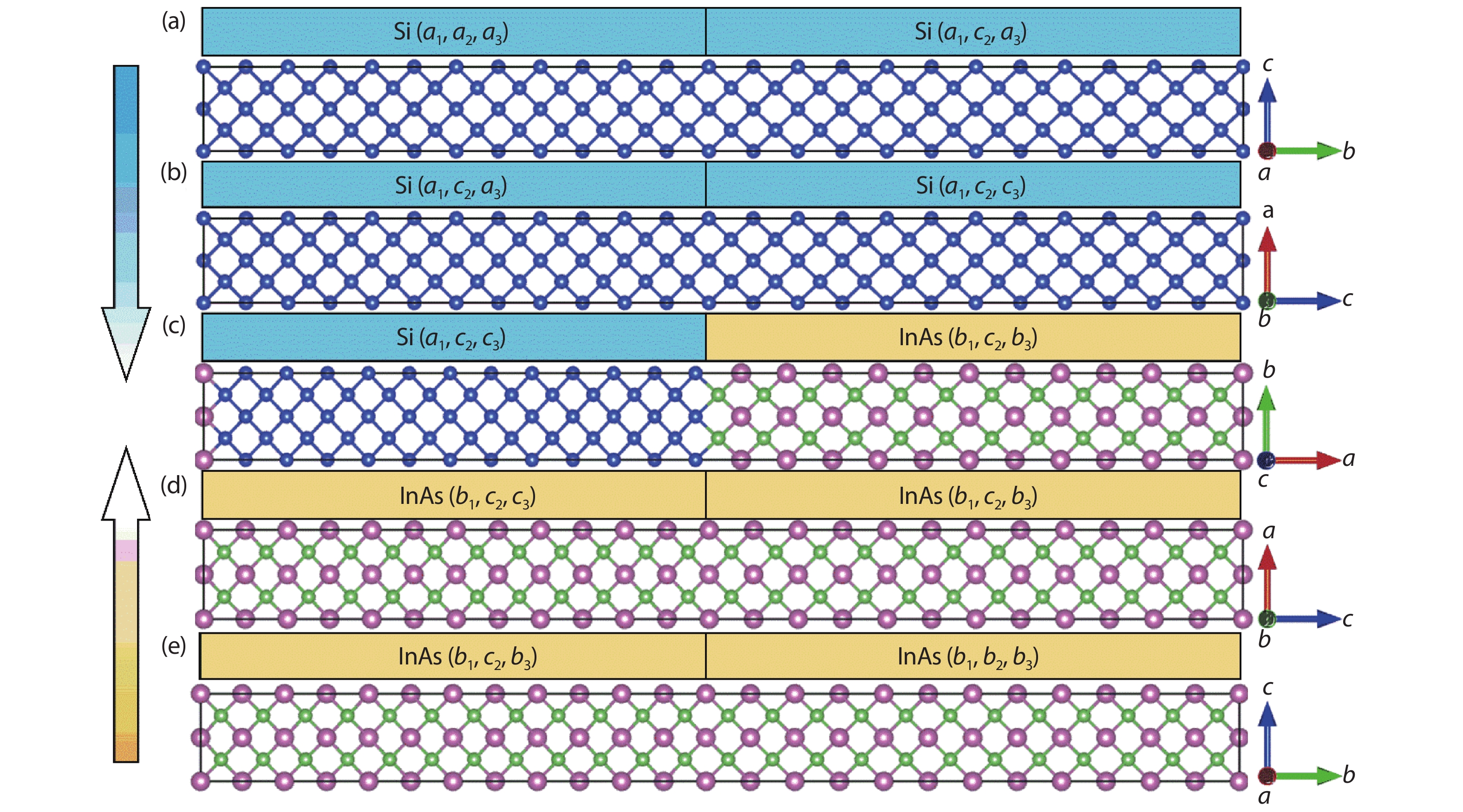
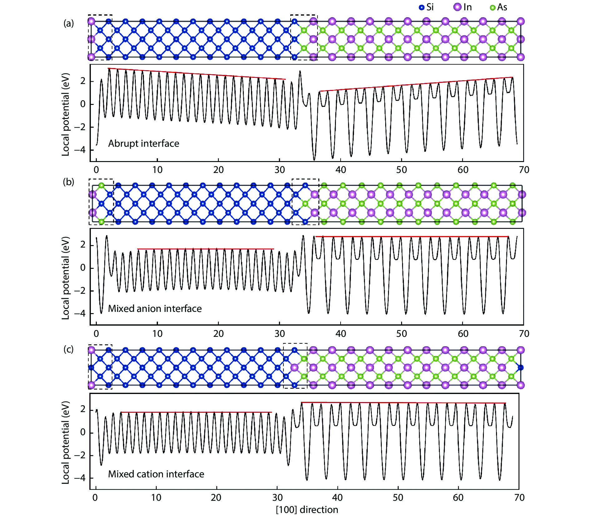
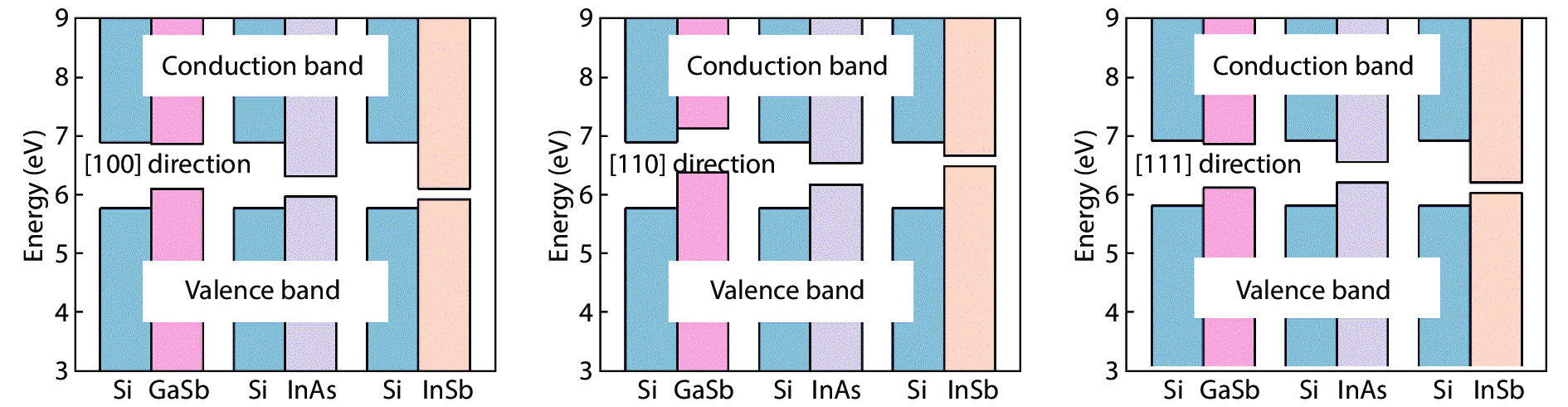
Band offset in semiconductors is a fundamental physical quantity that determines the performance of optoelectronic devices. However, the current method of calculating band offset is difficult to apply directly to the large-lattice-mismatched and heterovalent semiconductors because of the existing electric field and large strain at the interfaces. Here, we proposed a modified method to calculate band offsets for such systems, in which the core energy level shifts caused by heterovalent effects and lattice mismatch are estimated by interface reconstruction and the insertion of unidirectional strain structures as transitions, respectively. Taking the Si and III–V systems as examples, the results have the same accuracy as what is a widely used method for small-lattice-mismatched systems, and are much closer to the experimental values for the large-lattice-mismatched and heterovalent systems. Furthermore, by systematically studying the heterojunctions of Si and III–V semiconductors along different directions, it is found that the band offsets of Si/InAs and Si/InSb systems in [100], [110] and [111] directions belong to the type I, and could be beneficial for silicon-based luminescence performance. Our study offers a more reliable and direct method for calculating band offsets of large-lattice-mismatched and heterovalent semiconductors, and could provide theoretical support for the design of the high-performance silicon-based light sources.

J. Semicond.
2021, 42(11): 112201 doi: 10.1088/1674-4926/42/11/112201
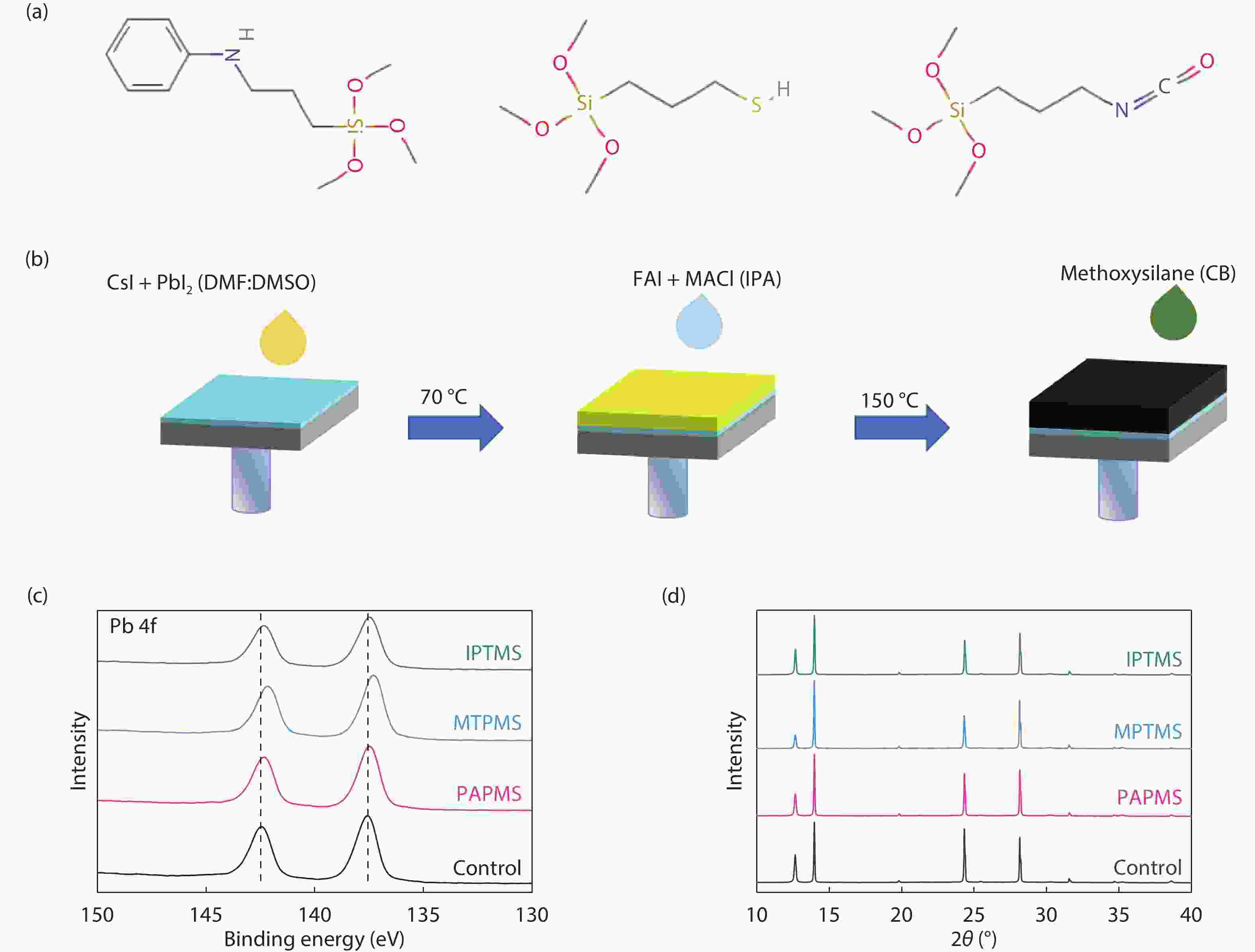
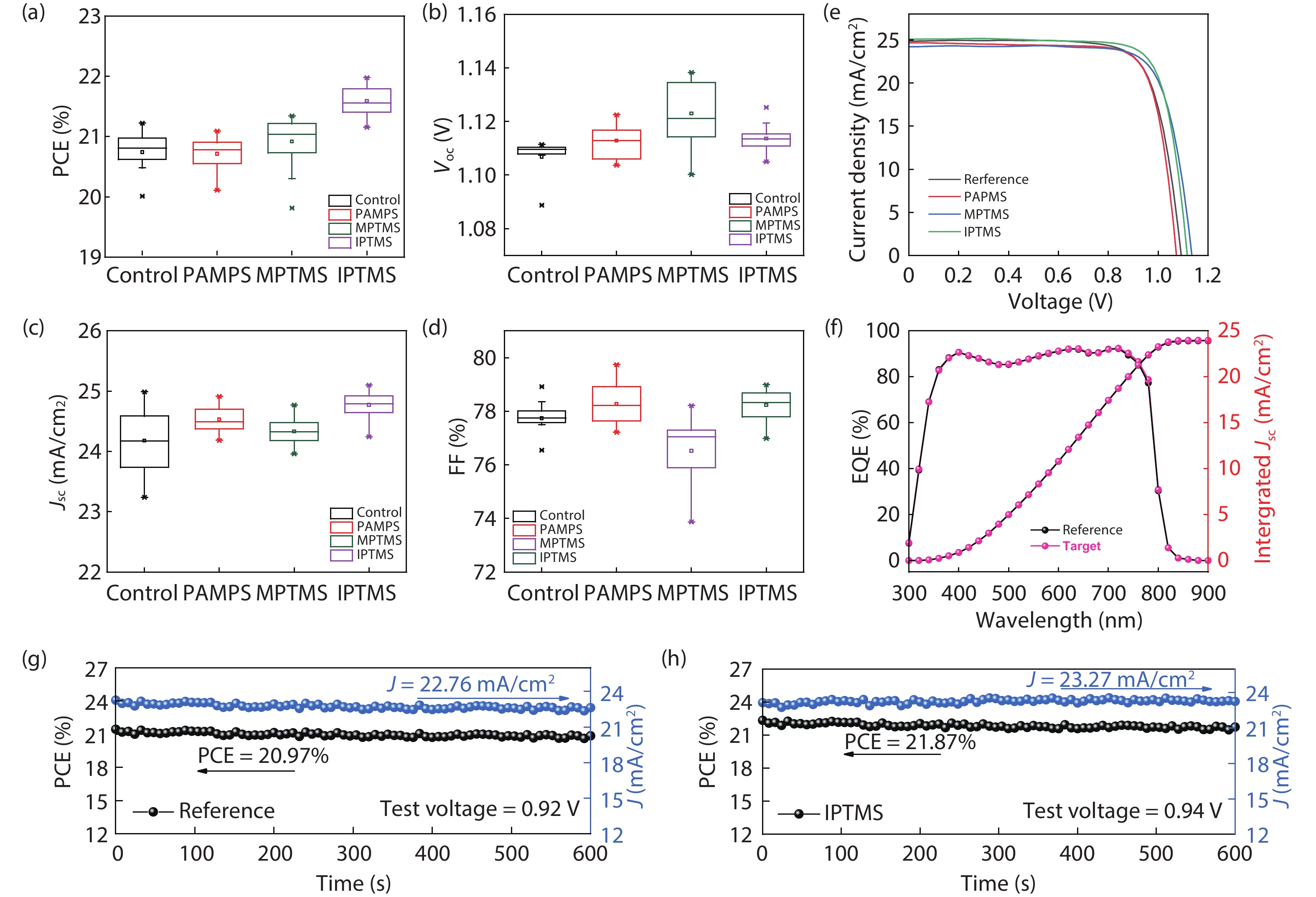
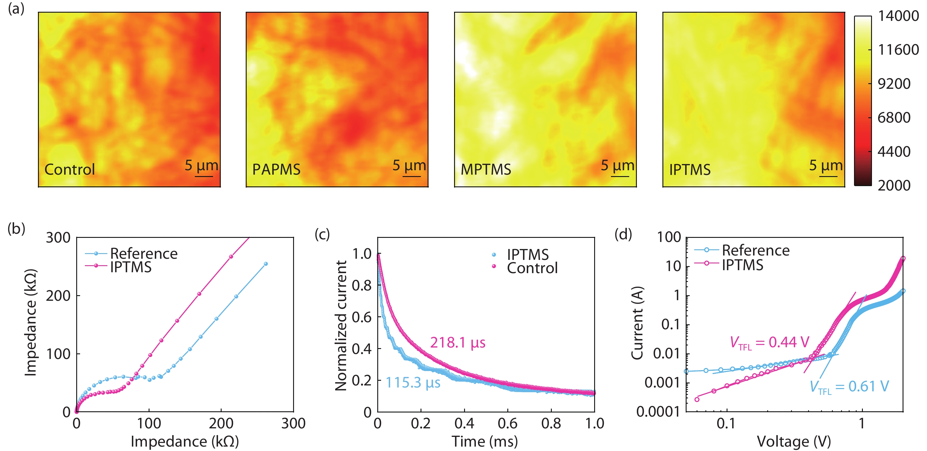
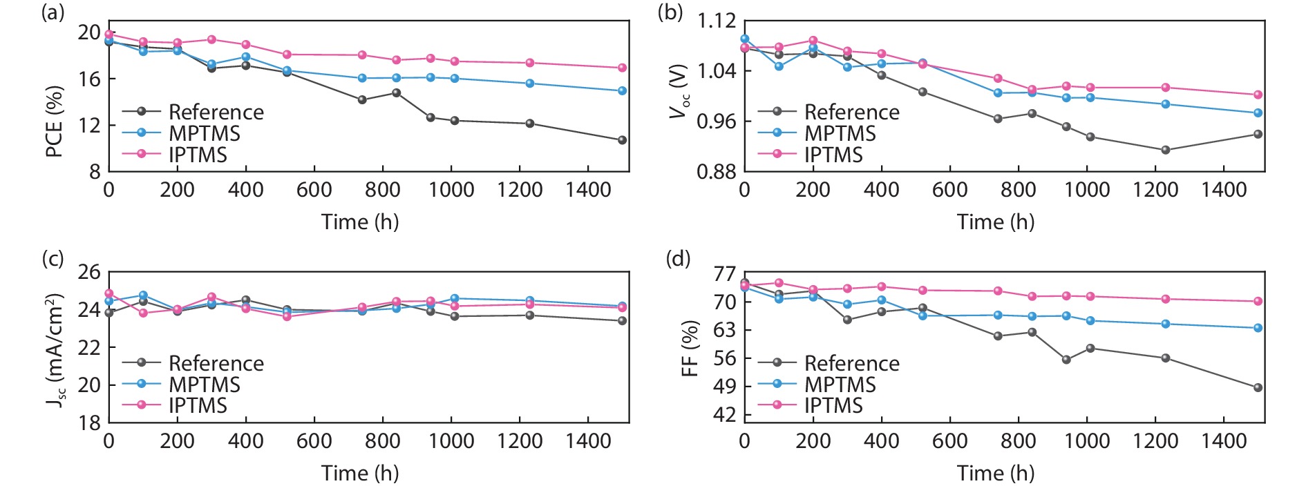
Interfacial engineering has made an outstanding contribution to the development of high-efficiency perovskite solar cells (PSCs). Here, we introduce an effective interface passivation strategy via methoxysilane molecules with different terminal groups. The power conversion efficiency (PCE) has increased from 20.97% to 21.97% after introducing a 3-isocyanatopropyltrimethoxy silane (IPTMS) molecule with carbonyl group, while a trimethoxy[3-(phenylamino)propyl] silane (PAPMS) molecule containing aniline group deteriorates the photovoltaic performance as a consequence of decreased open circuit voltage. The improved performance after IPTMS treatment is ascribed to the suppression of non-radiative recombination and enhancement of carrier transportation. In addition, the devices with carbonyl group modification exhibit outstanding thermal stability, which maintain 90% of its initial PCE after 1500 h exposure. This work provides a guideline for the design of passivation molecules aiming to deliver the efficiency and thermal stability simultaneously.

J. Semicond.
2021, 42(11): 112202 doi: 10.1088/1674-4926/42/11/112202

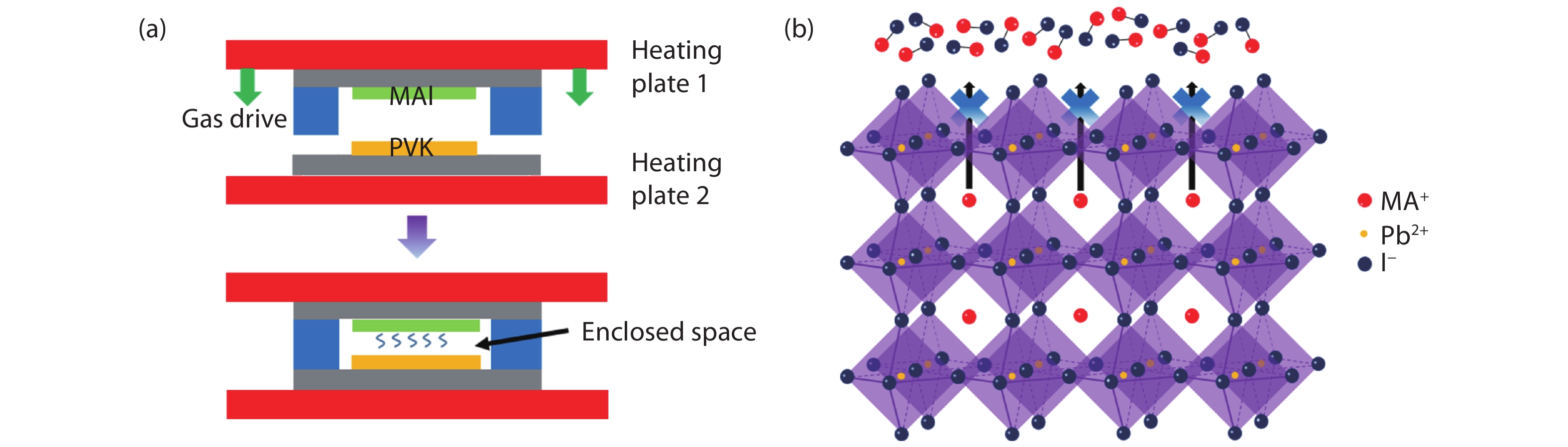
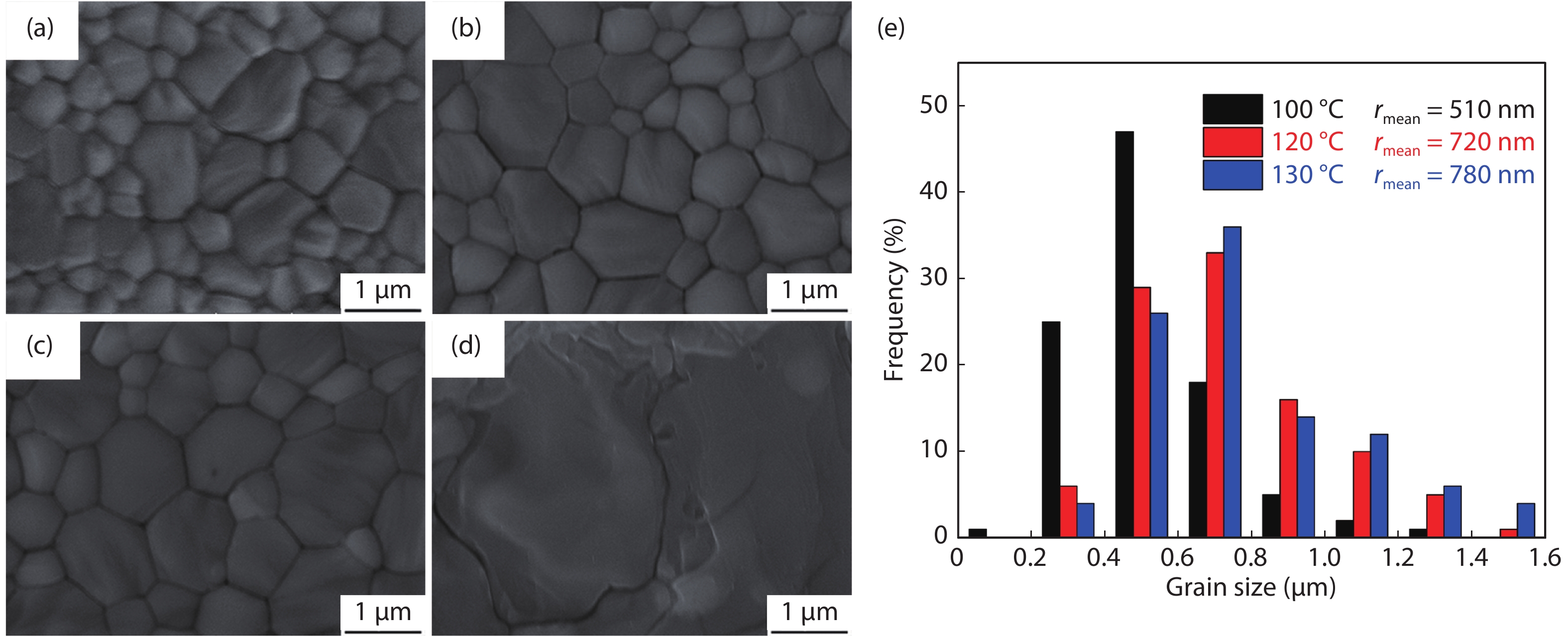
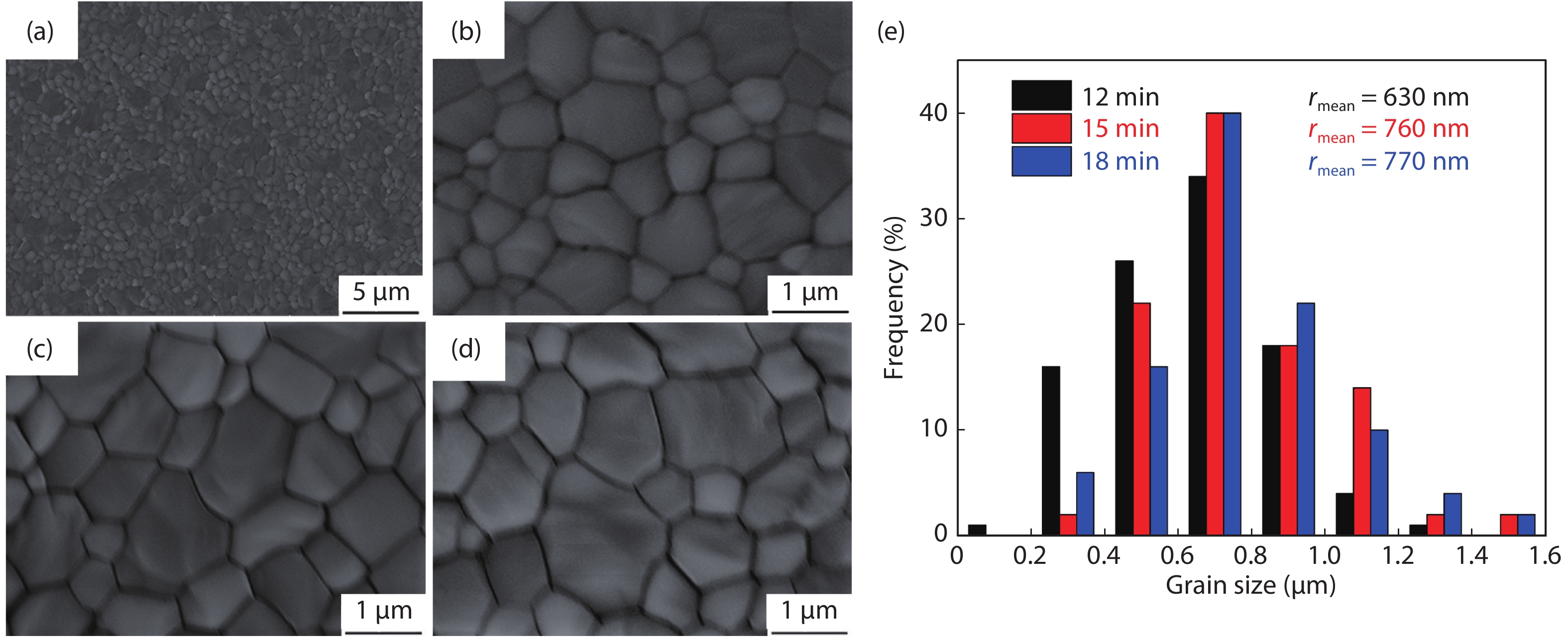
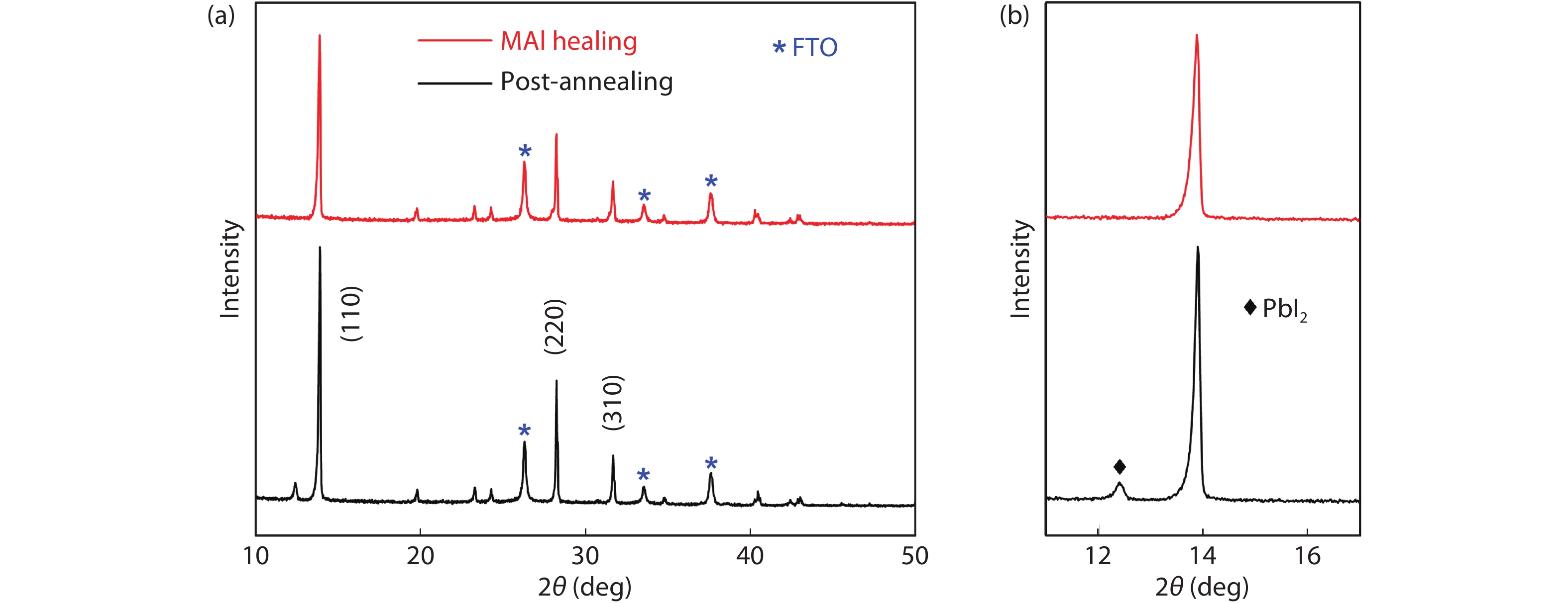
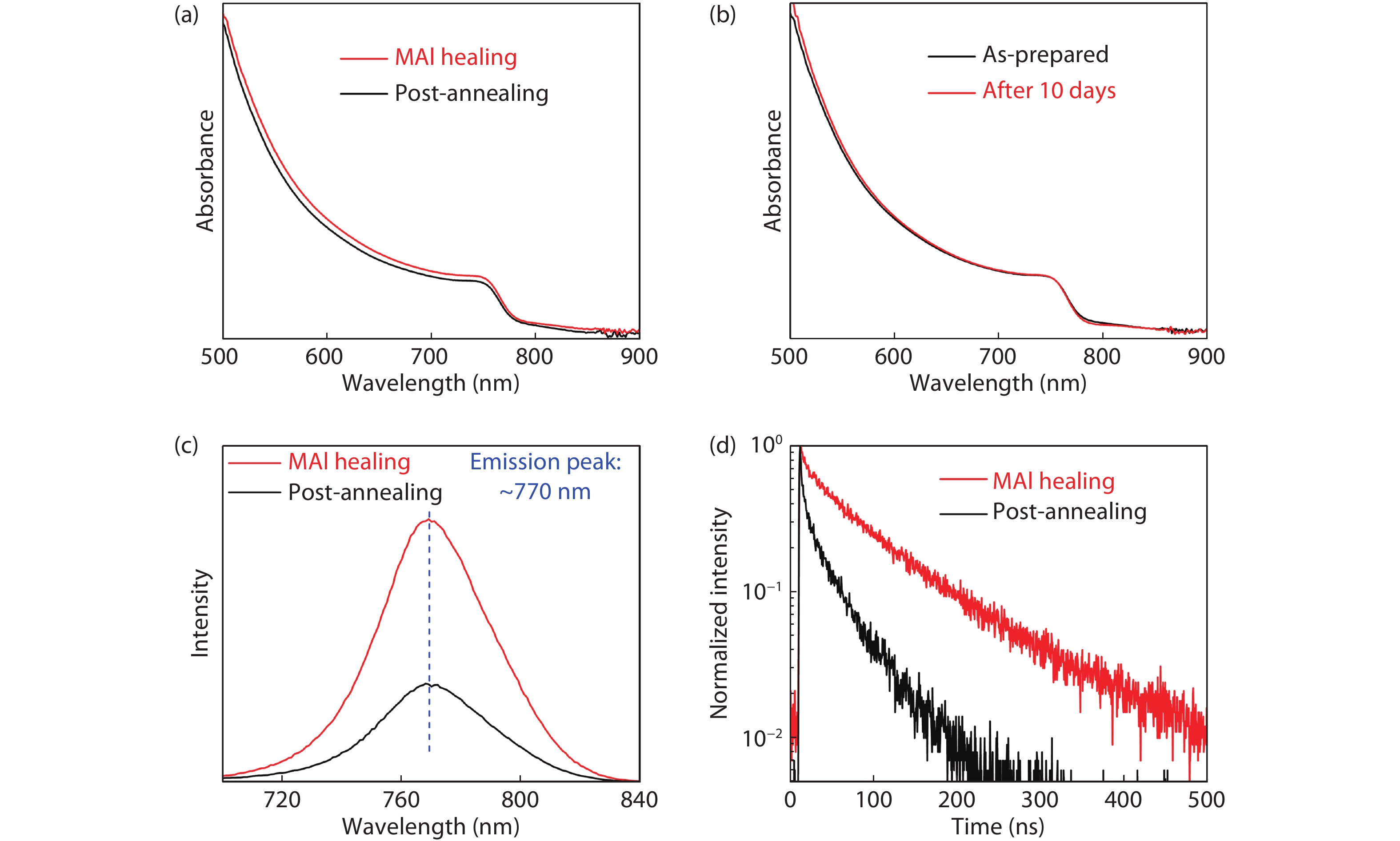
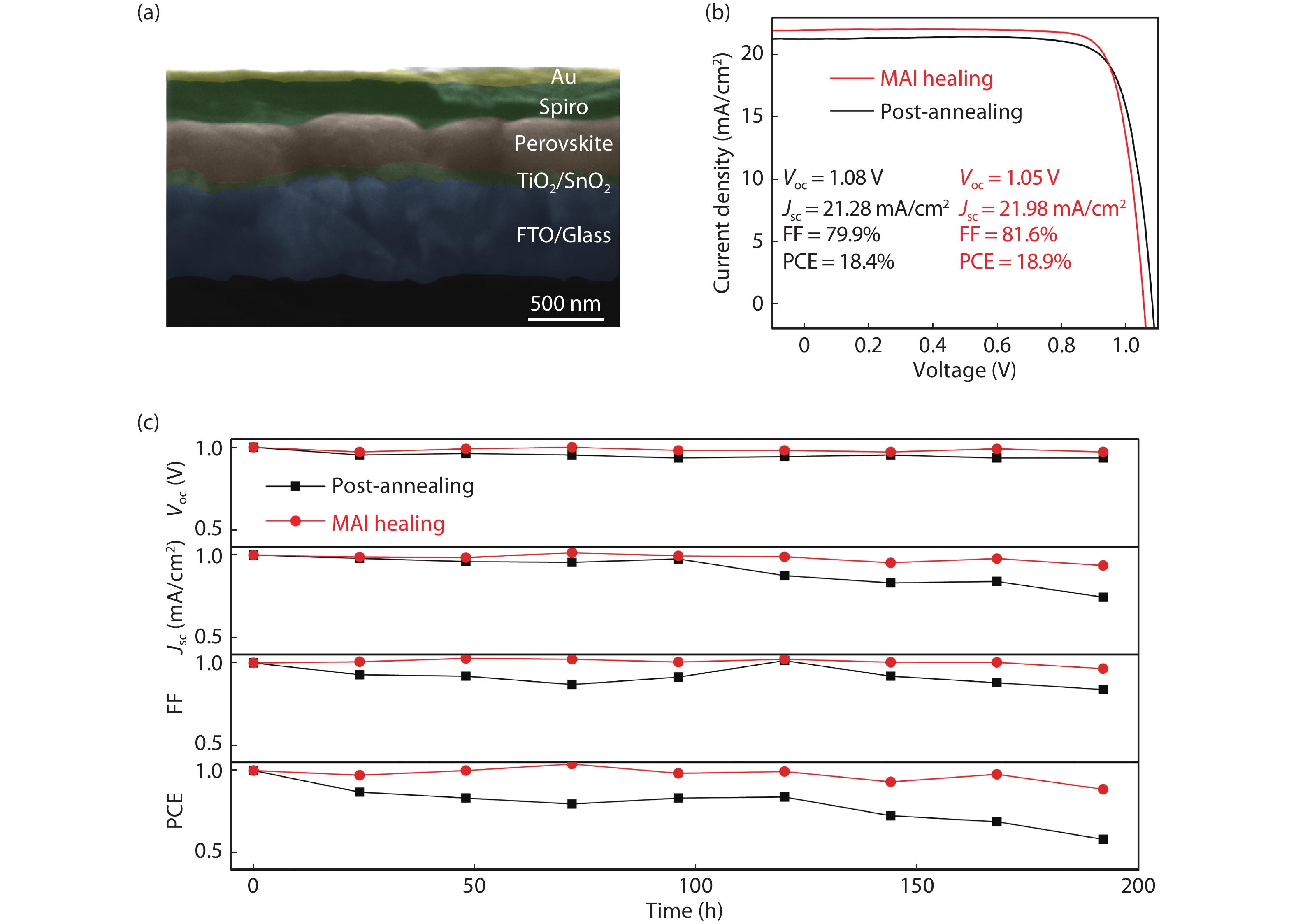
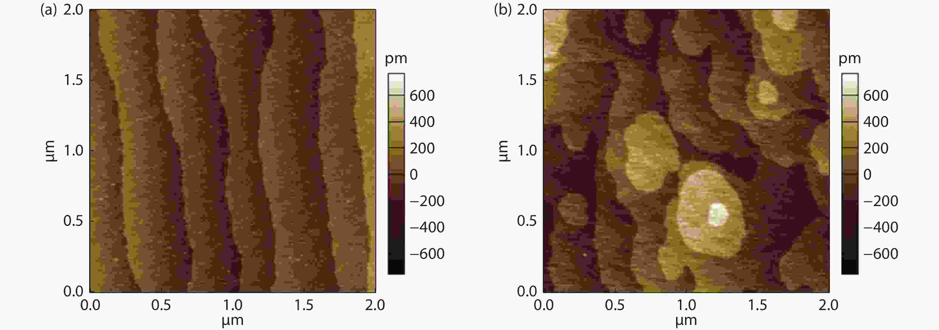
Repressing the thermal decomposition during the process of heat treatment plays an indispensable part in the preparation of perovskite films. Here, a methylammonium iodide healing method was applied to prevent the volatilization of the organic component inside the perovskite structure during the heat treatment. High-quality CH3NH3PbI3 film with a much larger grain size over 800 nm was successfully fabricated via this healing method. Besides, the absorption and photoluminescence intensity were also both improved. Finally, the best power conversion efficiency of 18.89% with a fill factor over 80% was realized in an n–i–p configuration while possessing outstanding stability. This work suggests that methylammonium iodide healing method is a reliable way to promote crystal growth and improve the photovoltaic performance and humidity stability of the CH3NH3PbI3 solar cells.

J. Semicond.
2021, 42(11): 112301 doi: 10.1088/1674-4926/42/11/112301
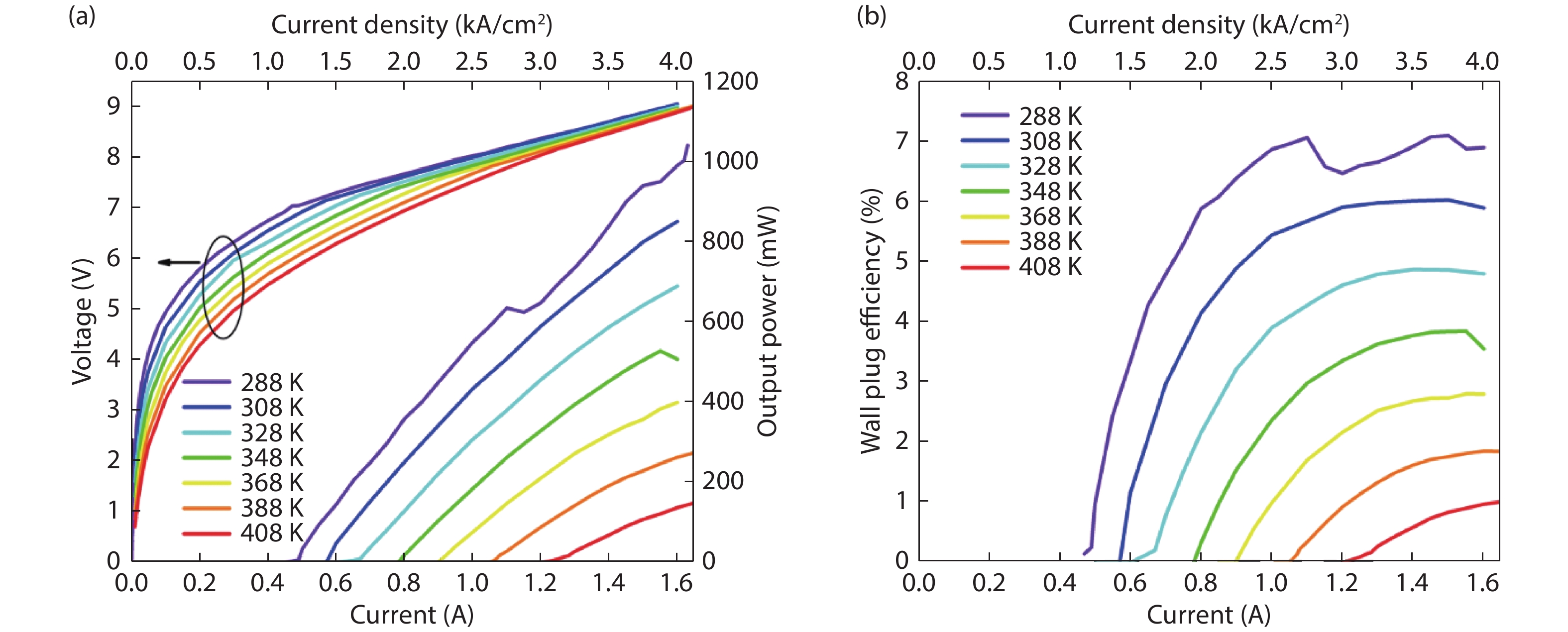
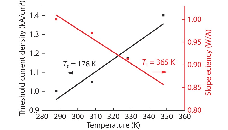
Robust quantum cascade laser (QCL) enduring high temperature continuous-wave (CW) operation is of critical importance for some applications. We report on the realization of lattice-matched InGaAs/InAlAs/InP QCL materials grown by metal-organic chemical vapor deposition (MOCVD). High interface quality structures designed for light emission at 8.5 μm are achieved by optimizing and precise controlling of growth conditions. A CW output power of 1.04 W at 288 K was obtained from a 4 mm-long and 10 μm-wide coated laser. Corresponding maximum wall-plug efficiency and threshold current density were 7.1% and 1.18 kA/cm2, respectively. The device can operate in CW mode up to 408 K with an output power of 160 mW.
J. Semicond.
2021, 42(11): 112701 doi: 10.1088/1674-4926/42/11/112701
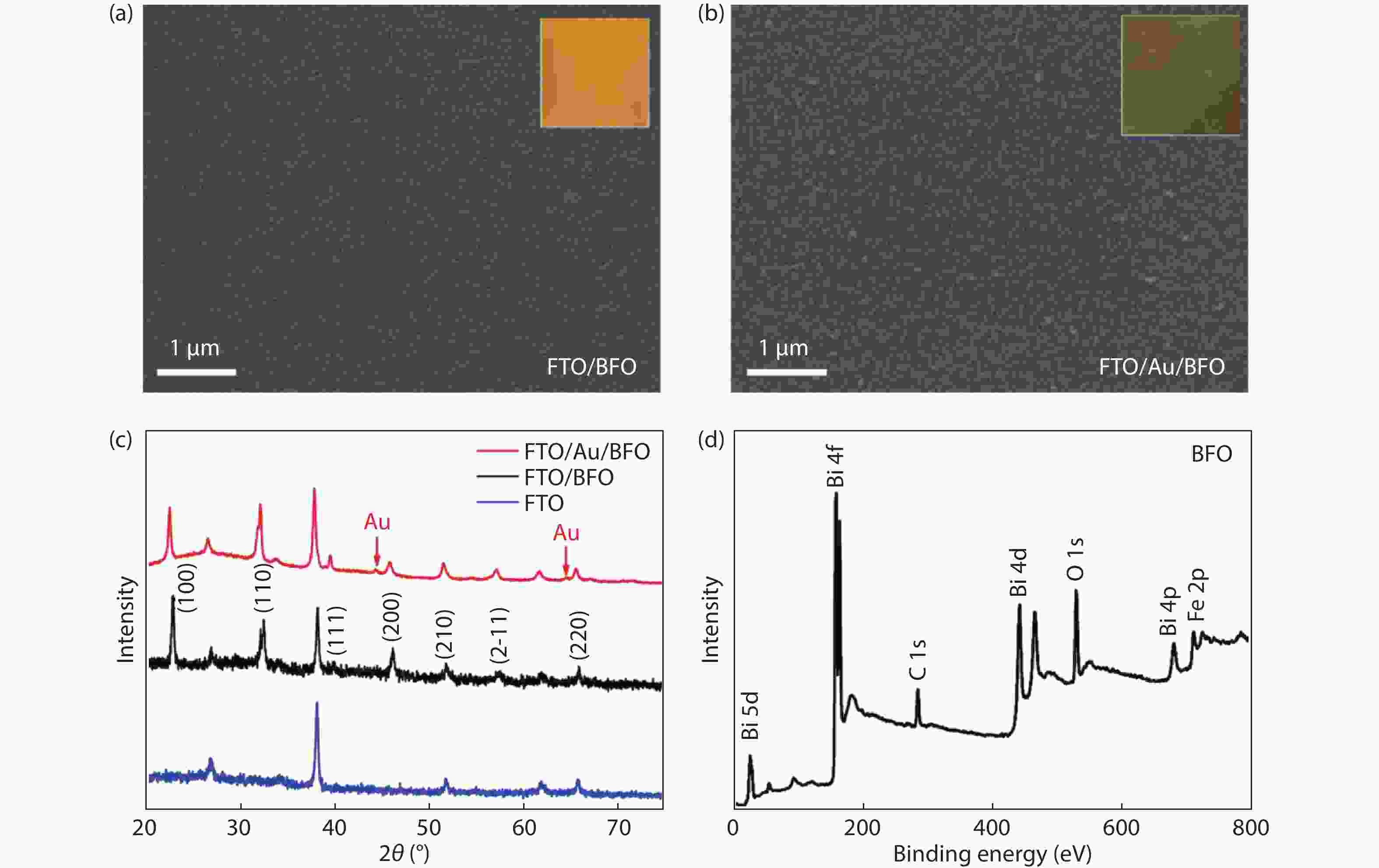
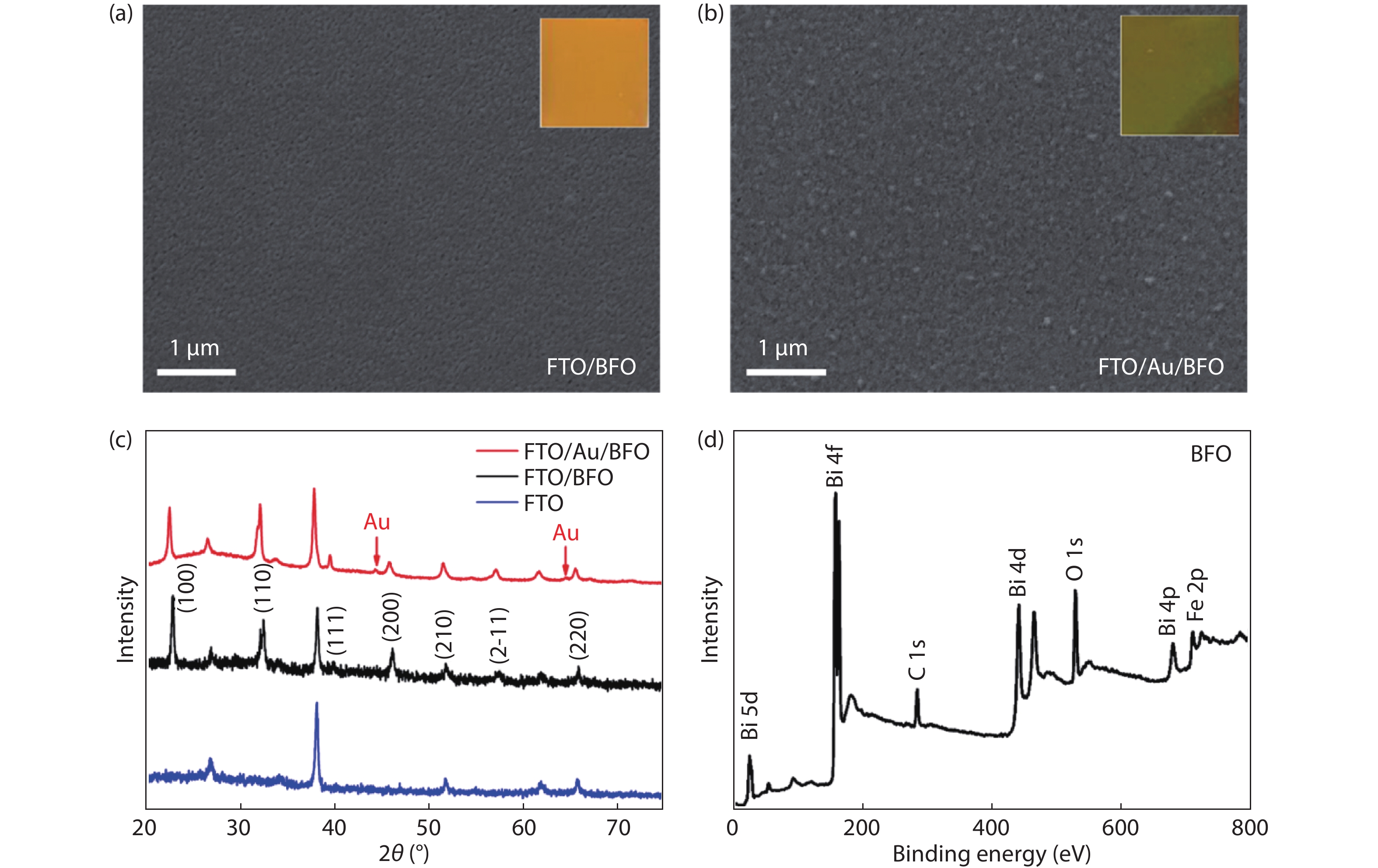
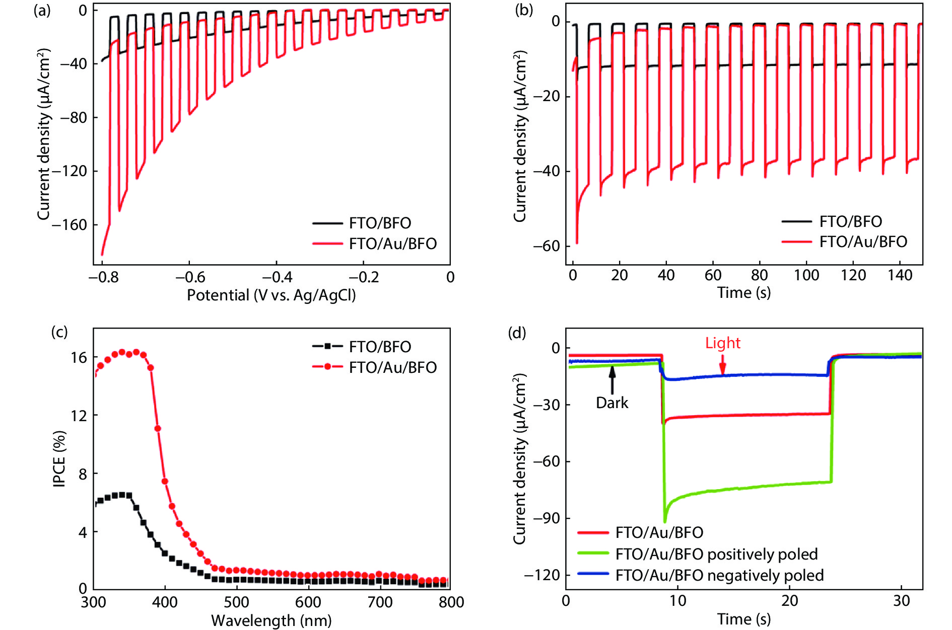
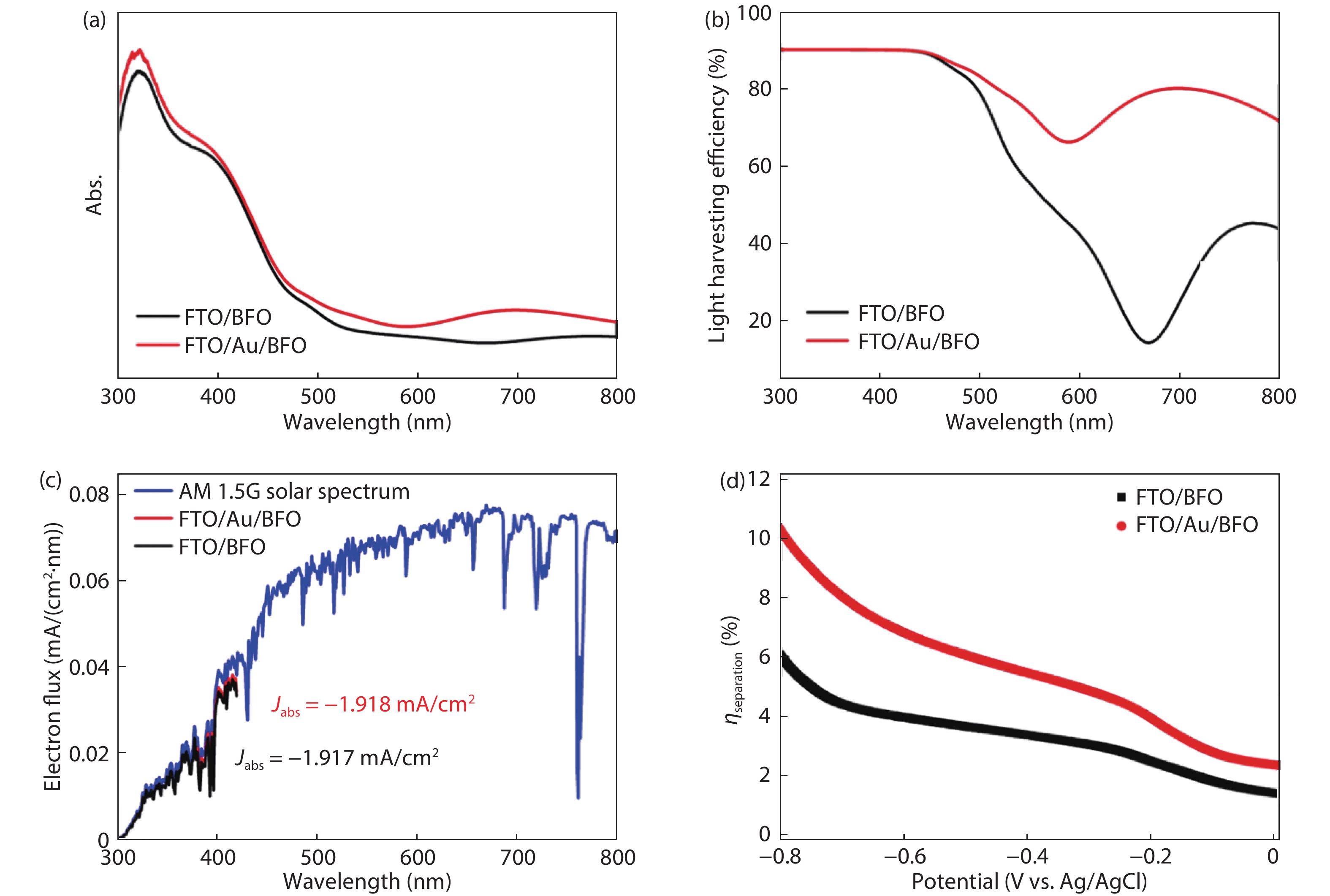
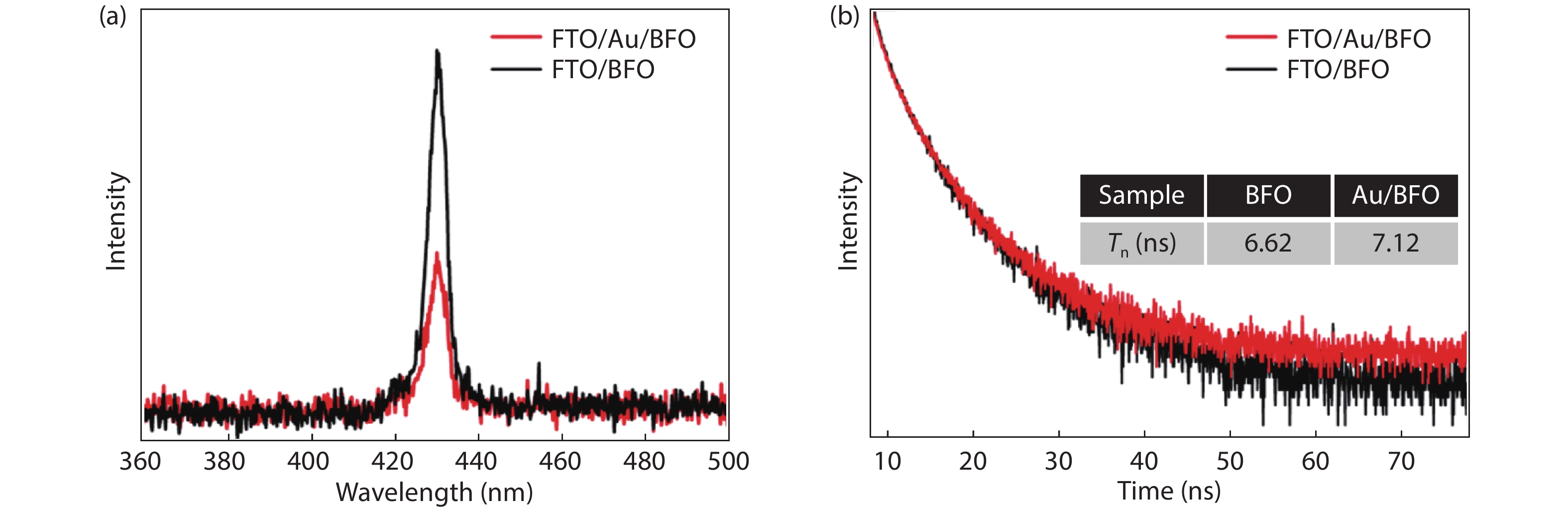
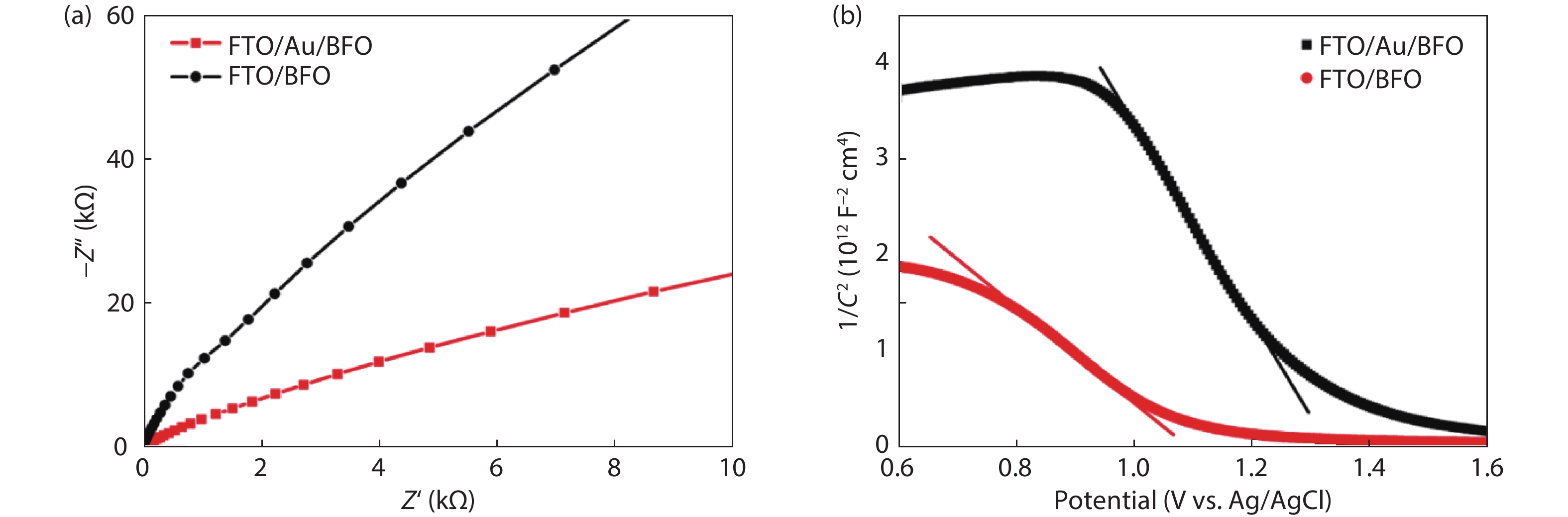
The inefficient separation of photogenerated carriers has become a serious problem that limits the photoelectrochemical (PEC) performance of semiconductors. Herein, a sol-gel method was used to prepare BiFeO3 ferroelectric thin films with FTO and FTO/Au as substrates, respectively. The polarization electric field of the ferroelectric can more effectively separate the carriers generated in the photoelectrode. Meanwhile, the introduction of an Au buffer layer can reduce the resistance in the process of charge transfer, accelerate the carrier migration, and enhance the efficiency of the charge separation. Under light irradiation, Au/BiFeO3 photoelectrode exhibited an extraordinary improvement in PEC water splitting compared with BiFeO3. In addition, the ferroelectric polarization electric field causes band bending, which further accelerates the separation of electrons and holes and improves the PEC performance of the photoelectrode. This work promotes the effective application of ferroelectric films in PEC water splitting.

J. Semicond.
2021, 42(11): 112801 doi: 10.1088/1674-4926/42/11/112801
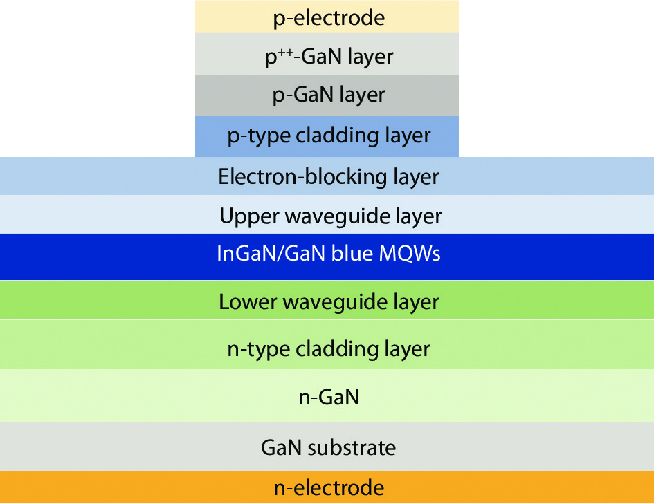
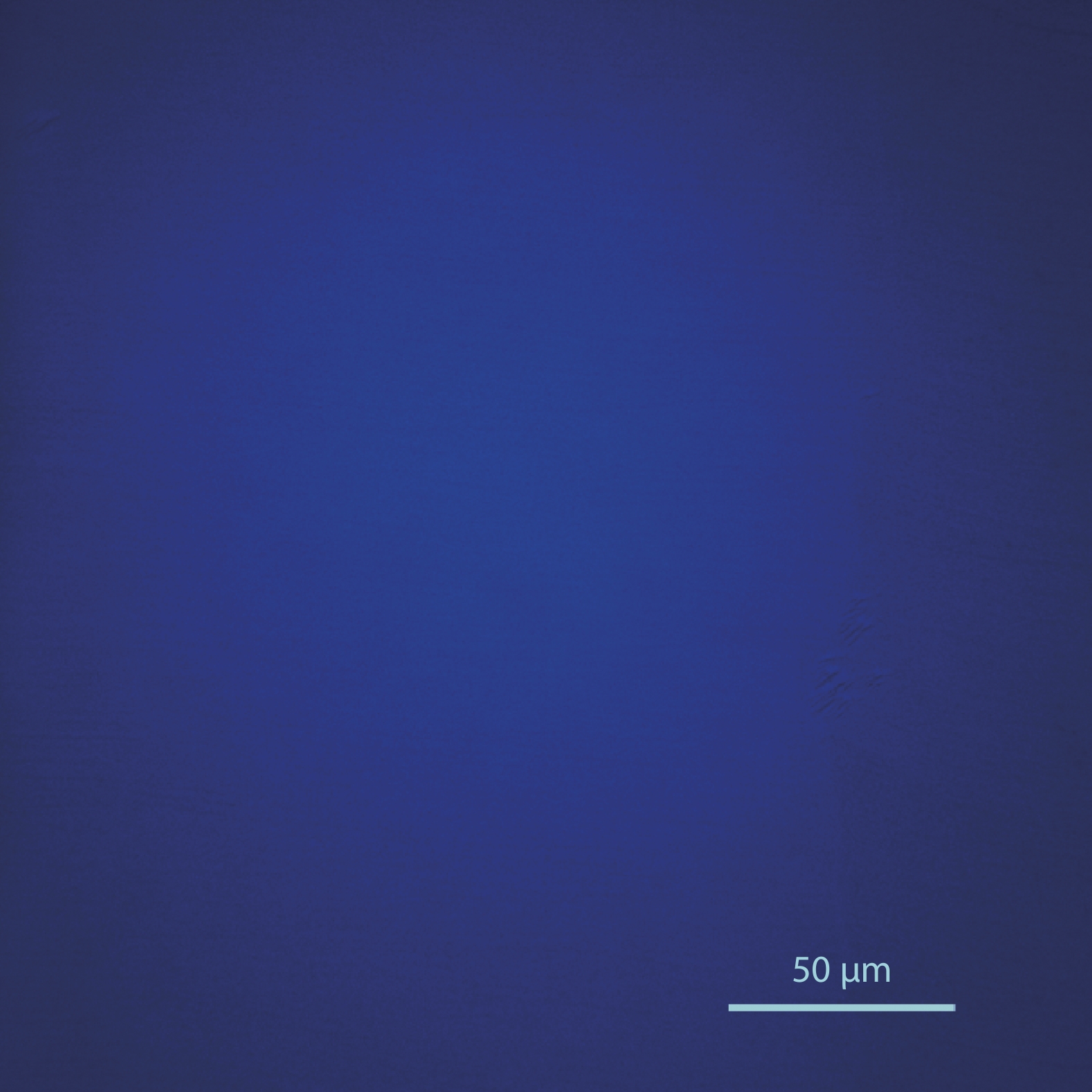
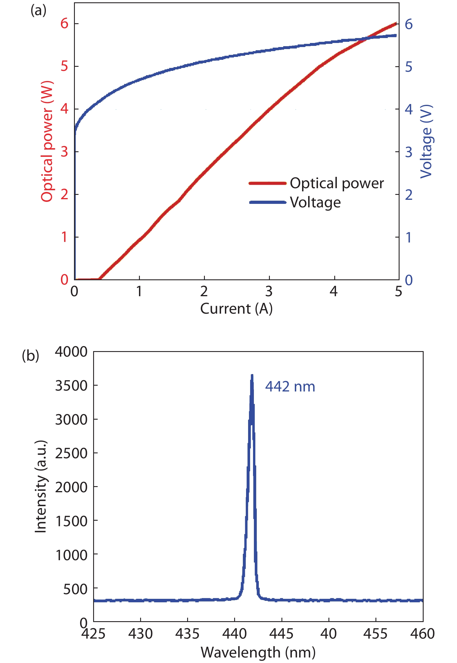
In this work, we reported the room-temperature continuous-wave operation of 6.0 W GaN-based blue laser diode (LD), and its stimulated emission wavelength is around 442 nm. The GaN-based high power blue LD is grown on a c-plane GaN substrate by metal organic chemical vapor deposition (MOCVD), and the width and length of the ridge waveguide structure are 30 and 1200 μm, respectively. The threshold current is about 400 mA, and corresponding threshold current density is 1.1 kA/cm2.
J. Semicond.
2021, 42(11): 112802 doi: 10.1088/1674-4926/42/11/112802

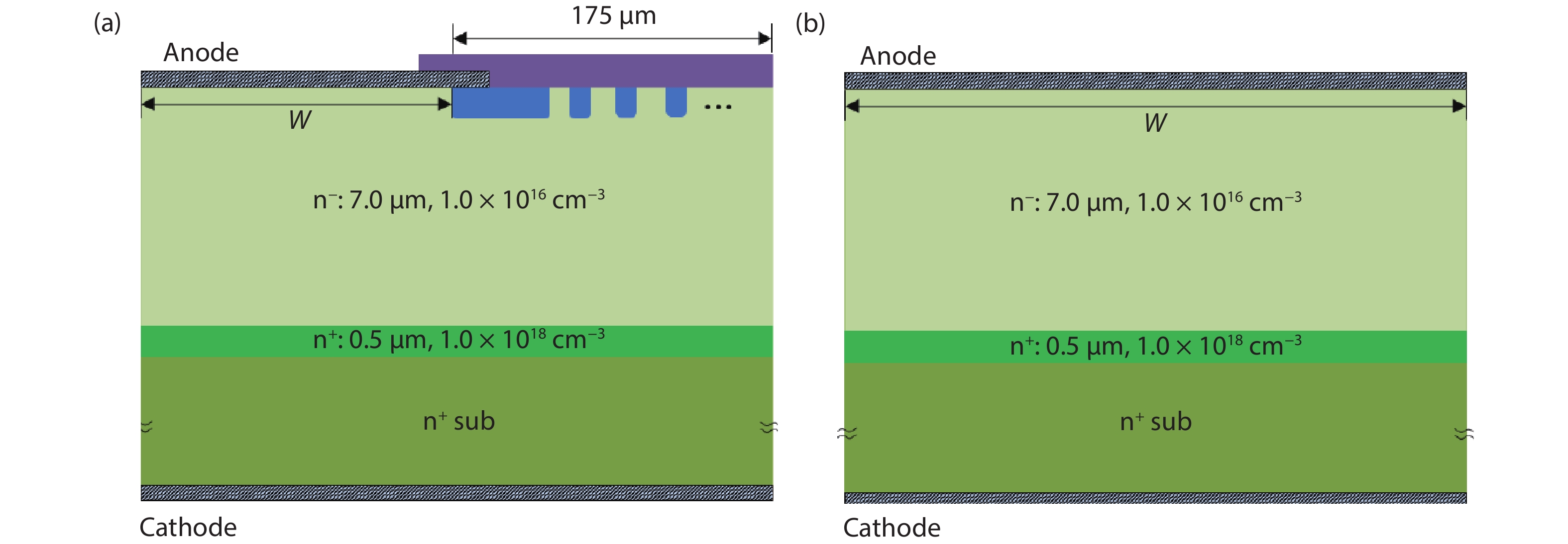
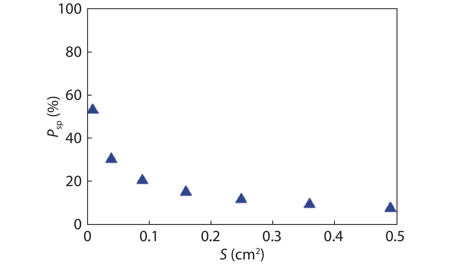
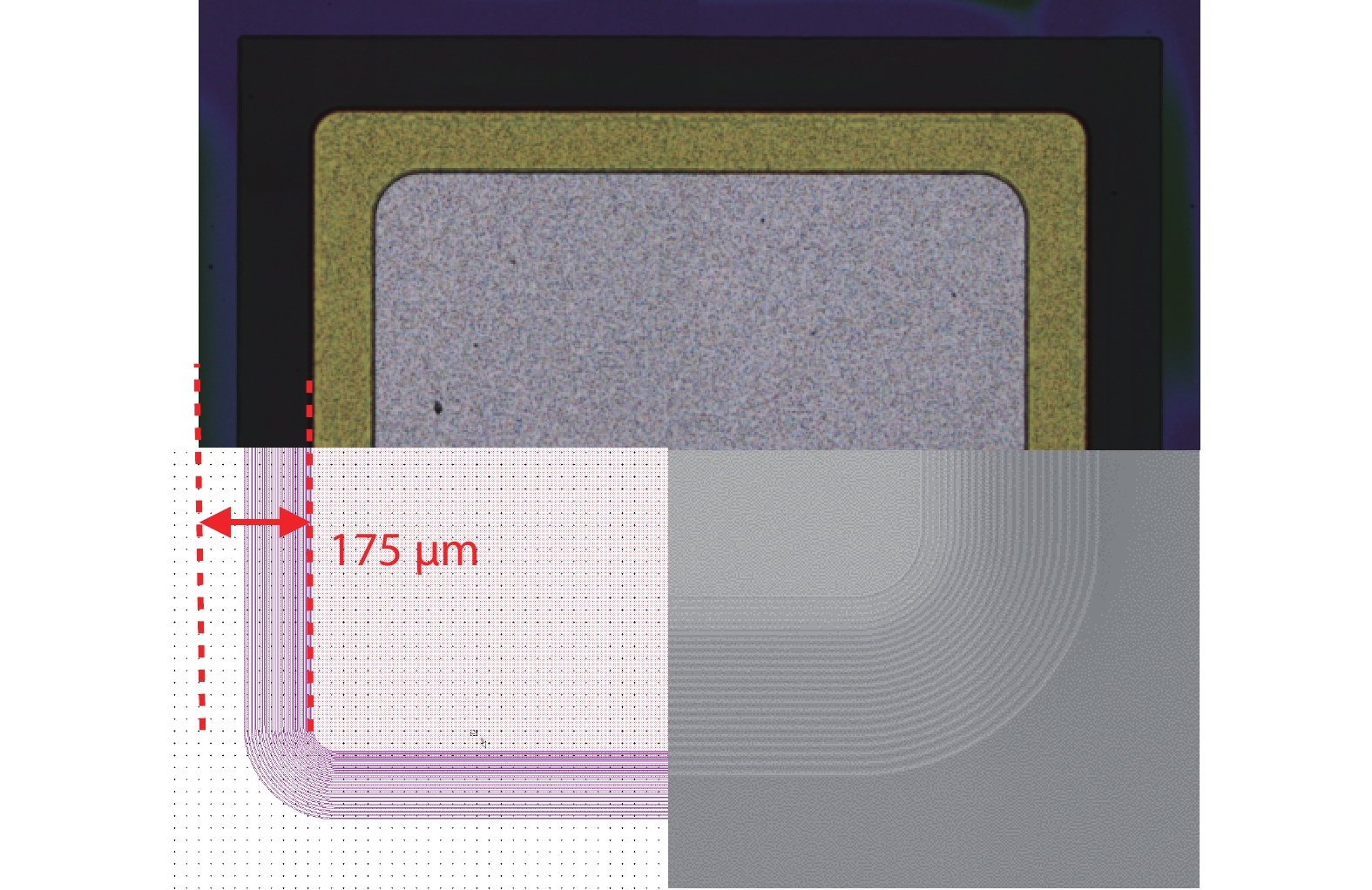
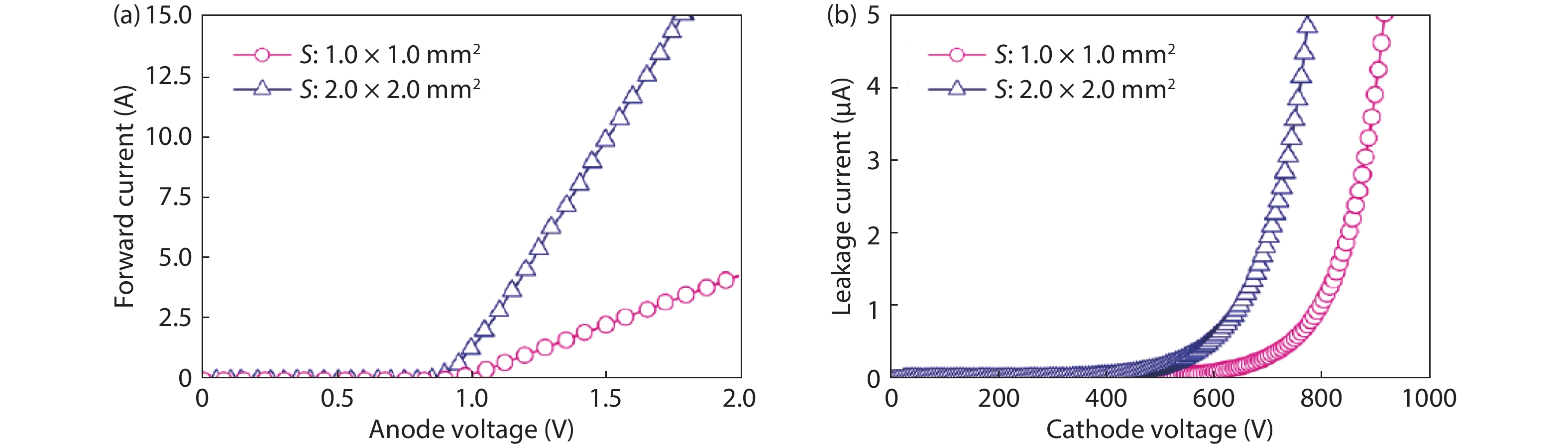
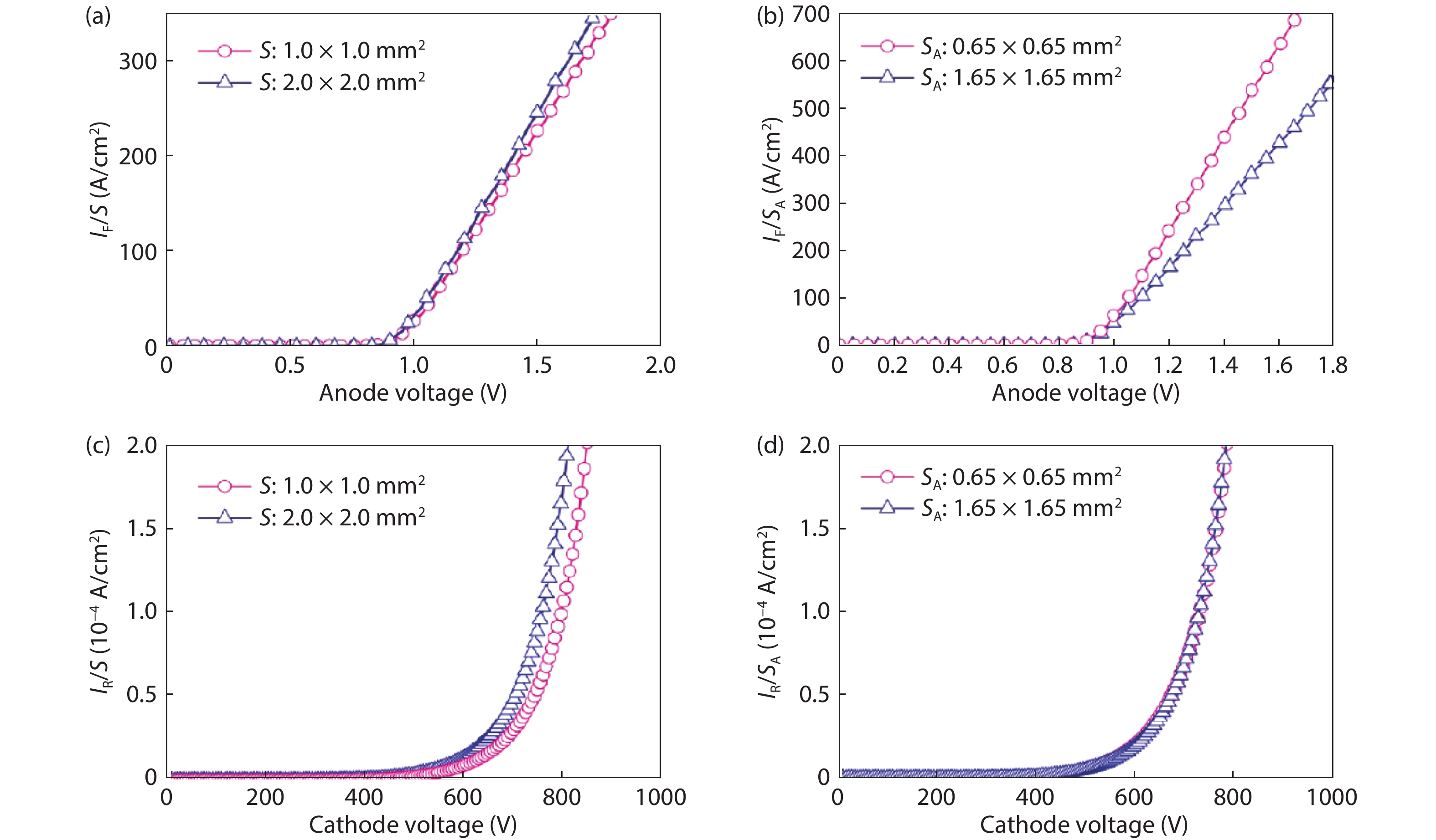
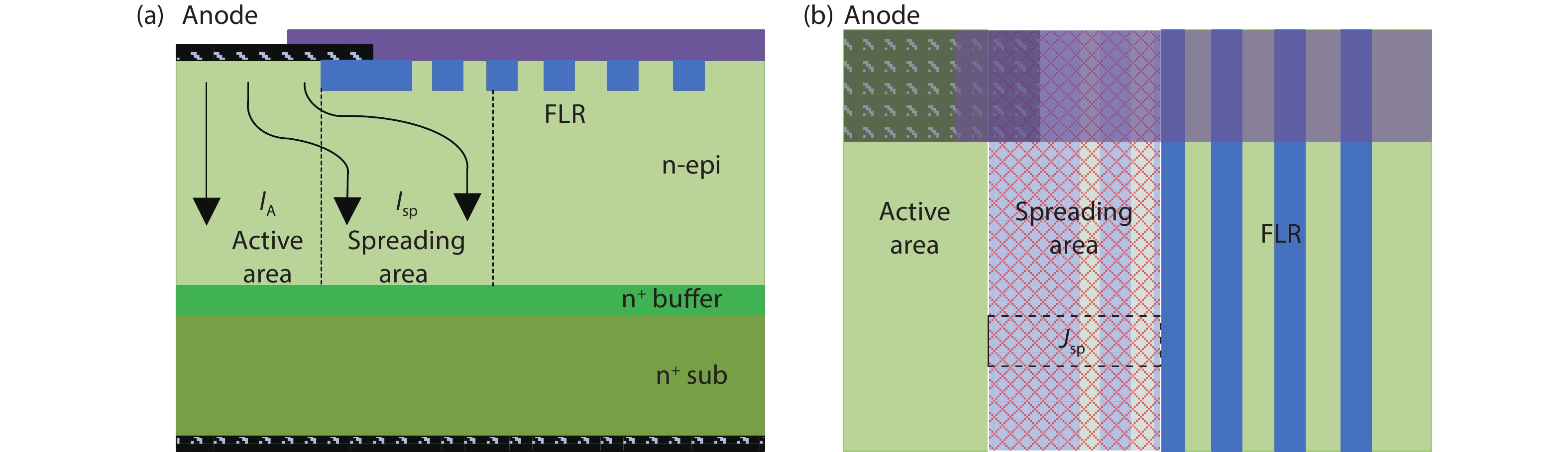
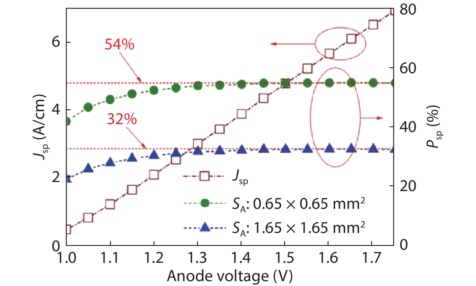
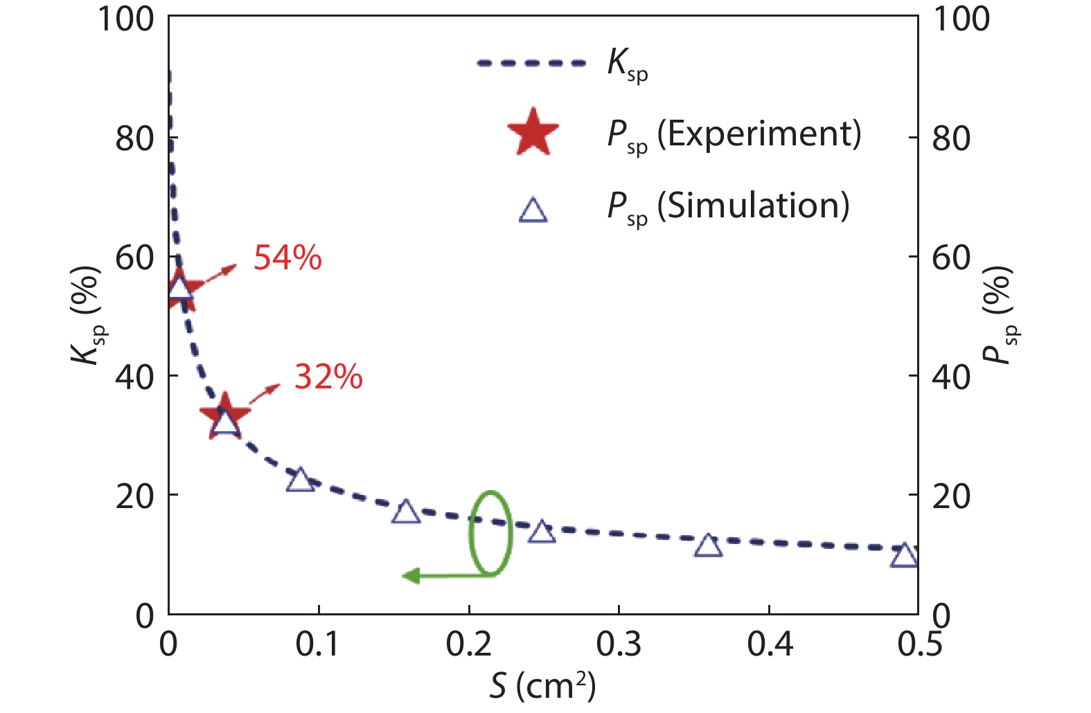
Lateral current spreading in the 4H-SiC Schottky barrier diode (SBD) chip is investigated. The 4H-SiC SBD chips with the same vertical parameters are simulated and fabricated. The results indicate that there is a fixed spreading resistance at on-state in current spreading region for a specific chip. The linear specific spreading resistance at the on-state is calculated to be 8.6 Ω/cm in the fabricated chips. The proportion of the lateral spreading current in total forward current (Psp) is related to anode voltage and the chip area. Psp is increased with the increase in the anode voltage during initial on-state and then tends to a stable value. The stable values of Psp of the two fabricated chips are 32% and 54%. Combined with theoretical analysis, the proportion of the terminal region and scribing trench in a whole chip (Ksp) is also calculated and compared with Psp. The Ksp values of the two fabricated chips are calculated to be 31.94% and 57.75%. The values of Ksp and Psp are close with each other in a specific chip. The calculated Ksp can be used to predict that when the chip area of SiC SBD becomes larger than 0.5 cm2, the value of Psp would be lower than 10%.
J. Semicond.
2021, 42(11): 114101 doi: 10.1088/1674-4926/42/11/114101

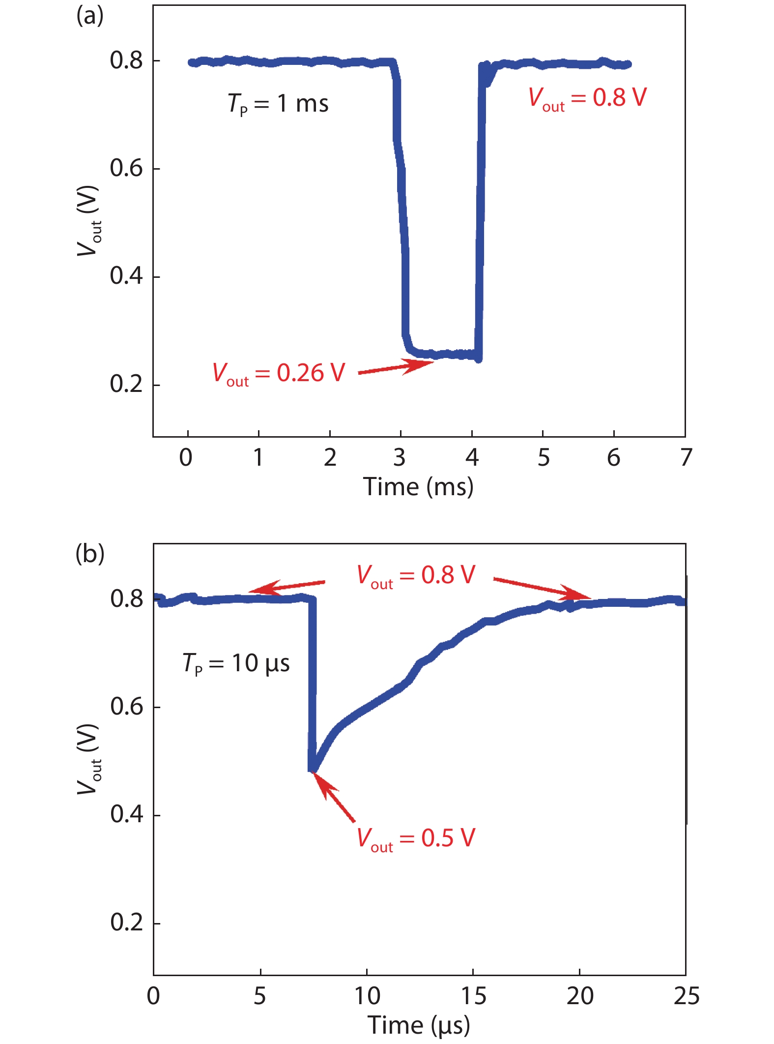
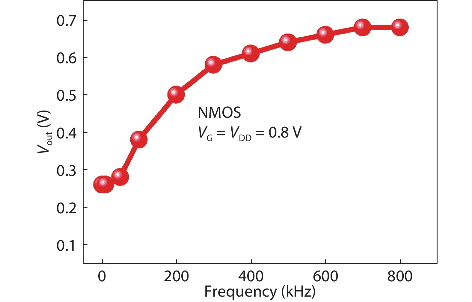
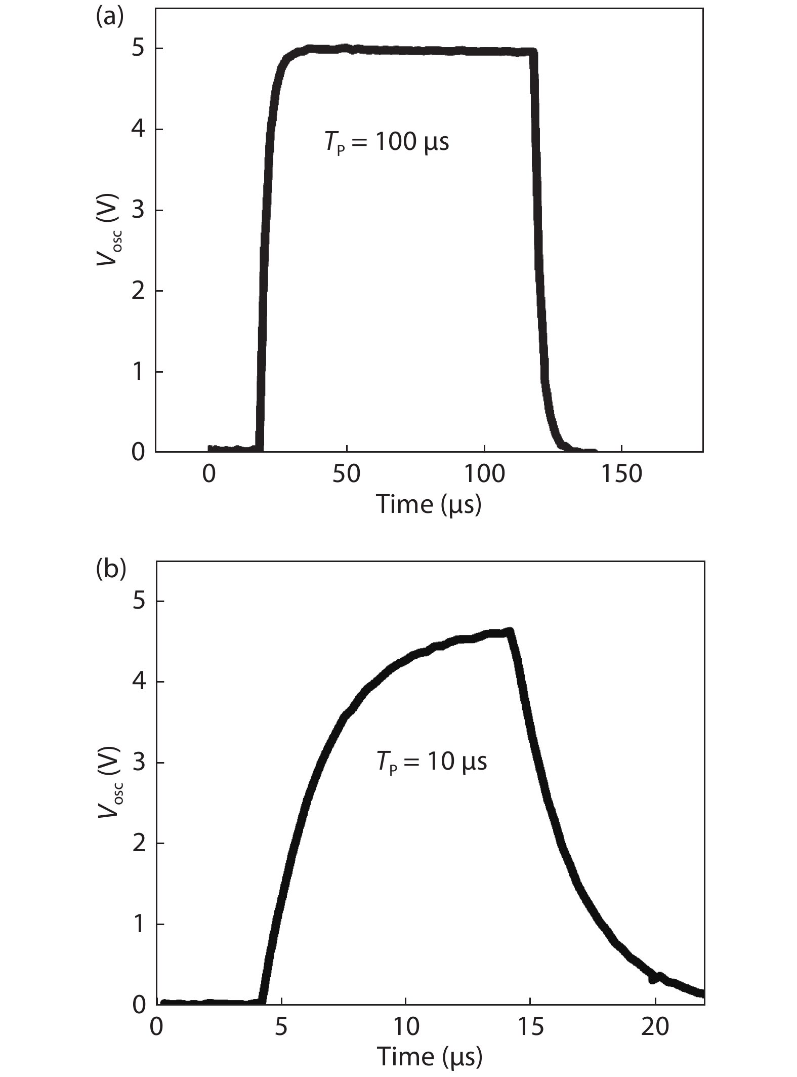
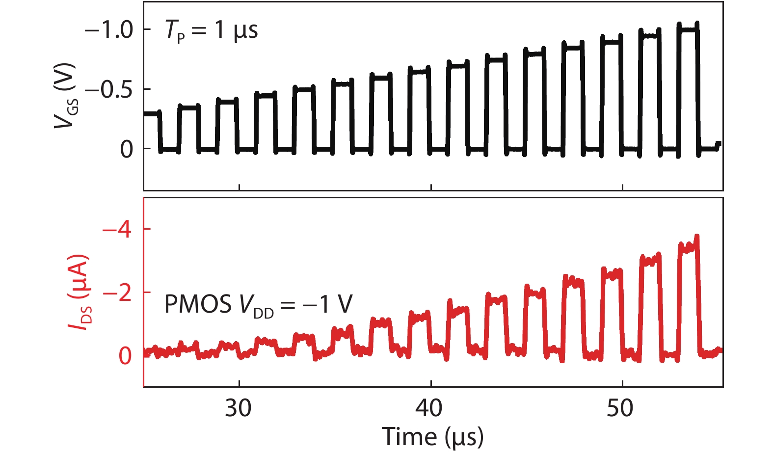
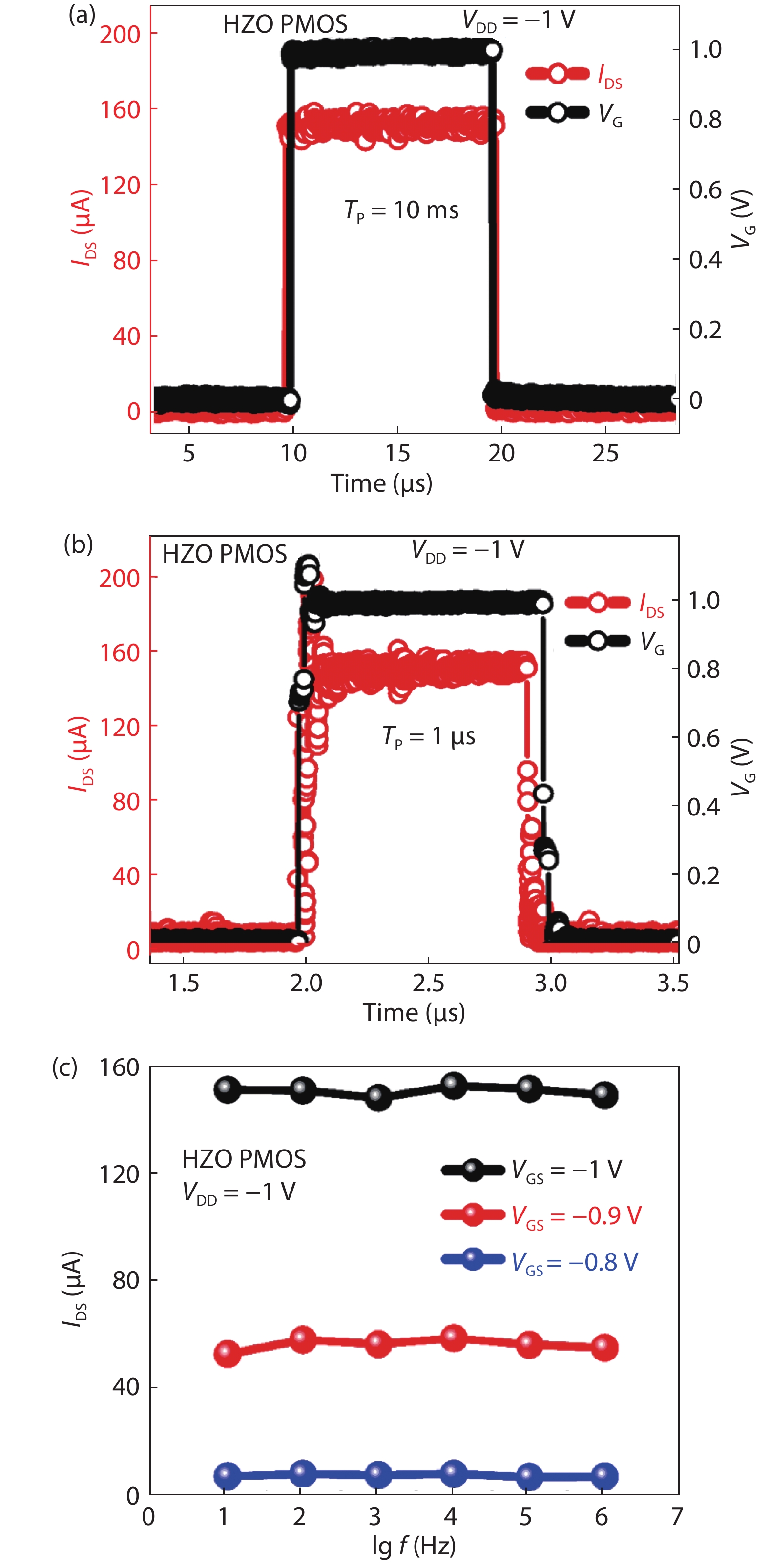
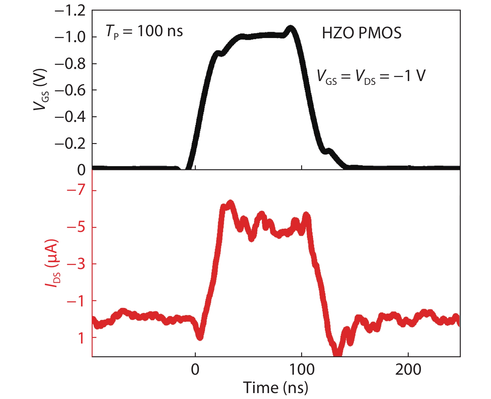
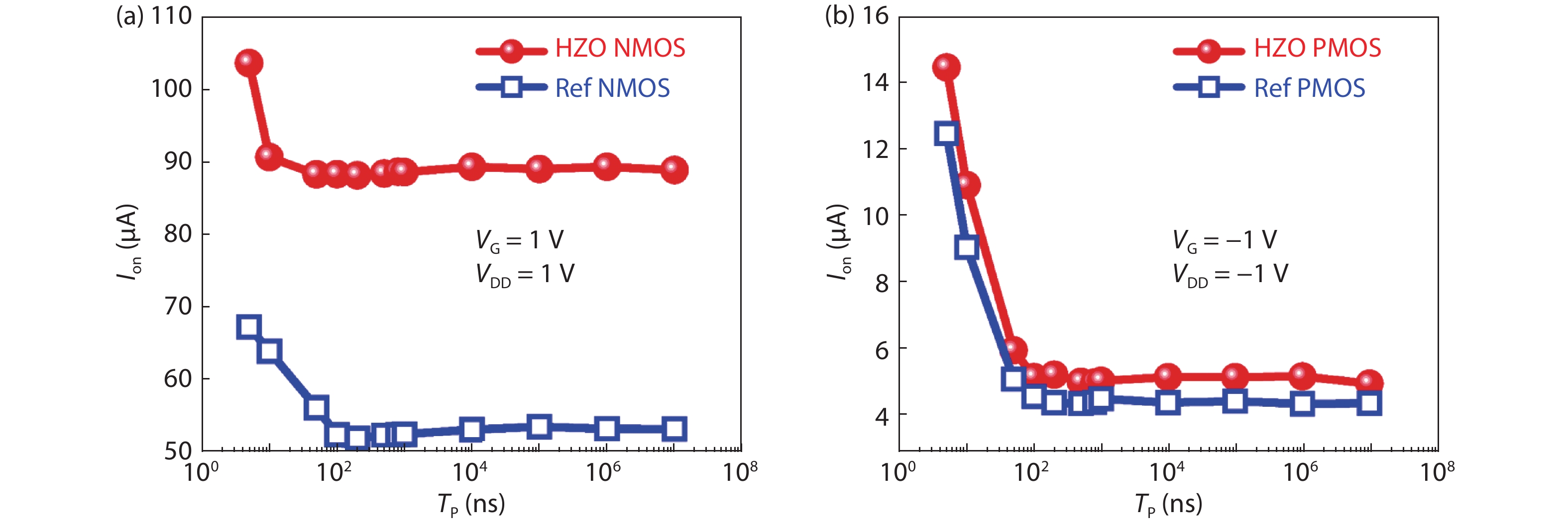
The HfO2-based ferroelectric field effect transistors (FeFET) have been widely studied for their ability in breaking the Boltzmann limit and the potential to be applied to low-power circuits. This article systematically investigates the transient response of negative capacitance (NC) fin field-effect transistors (FinFETs) through two kinds of self-built test schemes. By comparing the results with those of conventional FinFETs, we experimentally demonstrate that the on-current of the NC FinFET is not degraded in the MHz frequency domain. Further test results in the higher frequency domain show that the on-state current of the prepared NC FinFET increases with the decreasing gate pulse width at pulse widths below 100 ns and is consistently greater (about 80% with NC NMOS) than the on-state current of the conventional transistor, indicating the great potential of the NC FET for future high-frequency applications.
-01.jpg)


