


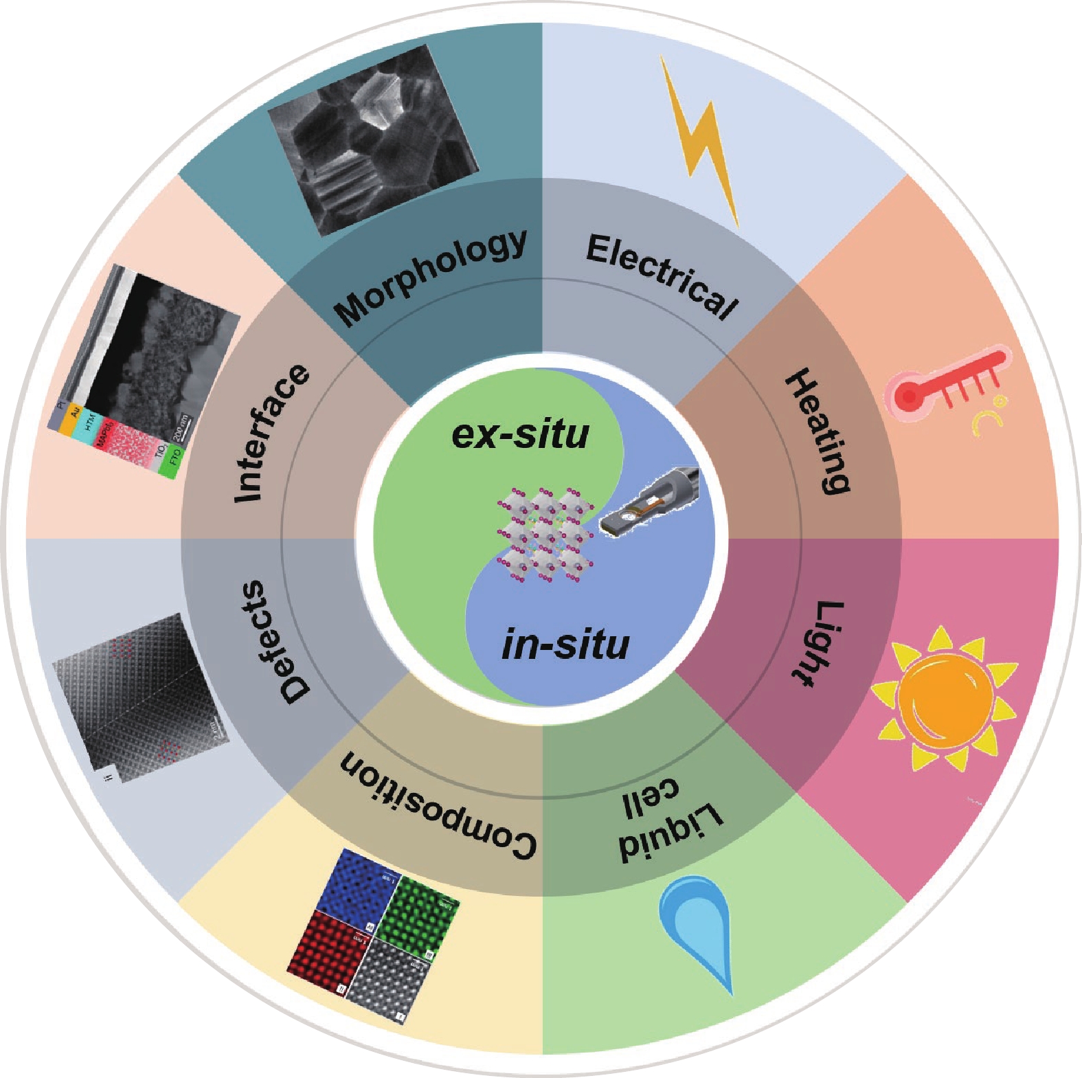
Fig. 1.
(Color online) Schematic illustration of advanced TEM characterization for halide perovskites.
REVIEWS
Xiaomei Wu, Xiaoxing Ke and Manling Sui
Corresponding author: Xiaoxing Ke, kexiaoxing@bjut.edu.cn; Manling Sui, mlsui@bjut.edu.cn
Abstract: Halide perovskites are strategically important in the field of energy materials. Along with the rapid development of the materials and related devices, there is an urgent need to understand the structure–property relationship from nanoscale to atomic scale. Much effort has been made in the past few years to overcome the difficulty of imaging limited by electron dose, and to further extend the investigation towards operando conditions. This review is dedicated to recent studies of advanced transmission electron microscopy (TEM) characterizations for halide perovskites. The irradiation damage caused by the interaction of electron beams and perovskites under conventional imaging conditions are first summarized and discussed. Low-dose TEM is then discussed, including electron diffraction and emerging techniques for high-resolution TEM (HRTEM) imaging. Atomic-resolution imaging, defects identification and chemical mapping on halide perovskites are reviewed. Cryo-TEM for halide perovskites is discussed, since it can readily suppress irradiation damage and has been rapidly developed in the past few years. Finally, the applications of in-situ TEM in the degradation study of perovskites under environmental conditions such as heating, biasing, light illumination and humidity are reviewed. More applications of emerging TEM characterizations are foreseen in the coming future, unveiling the structural origin of halide perovskite’s unique properties and degradation mechanism under operando conditions, so to assist the design of a more efficient and robust energy material.
Keywords: organic–inorganic hybrid perovskite solar cell materials, energy materials, scanning electron microscopy, transmission electron microscopy, irradiation damage
| [1] |
Jiang Q, Zhao Y, Zhang X W, et al. Surface passivation of perovskite film for efficient solar cells. Nat Photonics, 2019, 13, 460 doi: 10.1038/s41566-019-0398-2
|
| [2] |
Lin Y W, Lin G M, Sun B Y, et al. Nanocrystalline perovskite hybrid photodetectors with high performance in almost every figure of merit. Adv Funct Mater, 2018, 28, 1705589 doi: 10.1002/adfm.201705589
|
| [3] |
Ran J H, Dyck O, Wang X Z, et al. Electron-beam-related studies of halide perovskites: Challenges and opportunities. Adv Energy Mater, 2020, 10, 1903191 doi: 10.1002/aenm.201903191
|
| [4] |
Chen P F, Ong W J, Shi Z H, et al. Pb-based halide perovskites: Recent advances in photo(electro)catalytic applications and looking beyond. Adv Funct Mater, 2020, 30, 1909667 doi: 10.1002/adfm.201909667
|
| [5] |
Ye T, Pan L, Yang Y, et al. Synthesis of highly-oriented black CsPbI3 microstructures for high-performance solar cells. Chem Mater, 2020, 32, 3235 doi: 10.1021/acs.chemmater.0c00427
|
| [6] |
Green M A, Ho-Baillie A, Snaith H J. The emergence of perovskite solar cells. Nat Photonics, 2014, 8, 506 doi: 10.1038/nphoton.2014.134
|
| [7] |
Dong Q, Fang Y, Shao Y, et al. Electron-hole diffusion lengths > 175 μm in solution-grown CH3NH3PbI3 single crystals. Science, 2015, 347, 967 doi: 10.1126/science.aaa5760
|
| [8] |
Shi Z J, Guo J, Chen Y H, et al. Lead-free organic-inorganic hybrid perovskites for photovoltaic applications: Recent advances and perspectives. Adv Mater, 2017, 29, 1605005 doi: 10.1002/adma.201605005
|
| [9] |
Yang Z B, Rajagopal A, Jen A K Y. Ideal bandgap organic–inorganic hybrid perovskite solar cells. Adv Mater, 2017, 29, 1704418 doi: 10.1002/adma.201704418
|
| [10] |
Kim M, Jeong J, Lu H Z, et al. Conformal quantum dot–SnO2 layers as electron transporters for efficient perovskite solar cells. Science, 2022, 375, 302 doi: 10.1126/science.abh1885
|
| [11] |
Liu C, Sun J, Tan W L, et al. Alkali cation doping for improving the structural stability of 2D perovskite in 3D/2D PSCs. Nano Lett, 2020, 20, 1240 doi: 10.1021/acs.nanolett.9b04661
|
| [12] |
Xie F X, Chen C C, Wu Y Z, et al. Vertical recrystallization for highly efficient and stable formamidinium-based inverted-structure perovskite solar cells. Energy Environ Sci, 2017, 10, 1942 doi: 10.1039/C7EE01675A
|
| [13] |
Xiang W C, Wang Z W, Kubicki D J, et al. Europium-doped CsPbI2Br for stable and highly efficient inorganic perovskite solar cells. Joule, 2019, 3, 205 doi: 10.1016/j.joule.2018.10.008
|
| [14] |
Yang S, Niu W X, Wang A L, et al. Ultrathin two-dimensional organic-inorganic hybrid perovskite nanosheets with bright, tunable photoluminescence and high stability. Angew Chem Int Ed, 2017, 56, 4252 doi: 10.1002/anie.201701134
|
| [15] |
Sun Y, Yin Y, Pols M, et al. Engineering the phases and heterostructures of ultrathin hybrid perovskite nanosheets. Adv Mater, 2020, 32, 2002392 doi: 10.1002/adma.202002392
|
| [16] |
Su Y, Chen X J, Ji W Y, et al. Highly controllable and efficient synthesis of mixed-halide CsPbX3 (X = Cl, Br, I) perovskite QDs toward the tunability of entire visible light. ACS Appl Mater Interfaces, 2017, 9, 33020 doi: 10.1021/acsami.7b10612
|
| [17] |
Utzat H, Sun W W, Kaplan A E K, et al. Coherent single-photon emission from colloidal lead halide perovskite quantum dots. Science, 2019, 363, 1068 doi: 10.1126/science.aau7392
|
| [18] |
Filip M R, Hillman S, Haghighirad A A, et al. Band gaps of the lead-free halide double perovskites Cs2BiAgCl6 and Cs2BiAgBr6 from theory and experiment. J Phys Chem Lett, 2016, 7, 2579 doi: 10.1021/acs.jpclett.6b01041
|
| [19] |
Zhong H X, Yang M, Tang G, et al. Type-II lateral heterostructures of monolayer halide double perovskites for optoelectronic applications. ACS Energy Lett, 2020, 5, 2275 doi: 10.1021/acsenergylett.0c01046
|
| [20] |
McClure E T, Ball M R, Windl W, et al. Cs2AgBiX6 (X = Br, Cl): New visible light absorbing, lead-free halide perovskite semiconductors. Chem Mater, 2016, 28, 1348 doi: 10.1021/acs.chemmater.5b04231
|
| [21] |
Wu C C, Zhang Q H, Liu Y, et al. The dawn of lead-free perovskite solar cell: Highly stable double perovskite Cs2AgBiBr6 film. Adv Sci, 2018, 5, 1700759 doi: 10.1002/advs.201700759
|
| [22] |
Volonakis G, Haghighirad A A, Milot R L, et al. Cs2InAgCl6: A new lead-free halide double perovskite with direct band gap. J Phys Chem Lett, 2017, 8, 772 doi: 10.1021/acs.jpclett.6b02682
|
| [23] |
Li Z Z, Yin W J. Recent progress in Pb-free stable inorganic double halide perovskites. J Semicond, 2018, 39, 071003 doi: 10.1088/1674-4926/39/7/071003
|
| [24] |
Xiao Z W, Yan Y F. Progress in theoretical study of metal halide perovskite solar cell materials. Adv Energy Mater, 2017, 7, 1701136 doi: 10.1002/aenm.201701136
|
| [25] |
Yang Y, Sun Y B, Jiang Y S. Structure and photocatalytic property of perovskite and perovskite-related compounds. Mater Chem Phys, 2006, 96, 234 doi: 10.1016/j.matchemphys.2005.07.007
|
| [26] |
Zhang H, Fu X, Tang Y, et al. Phase segregation due to ion migration in all-inorganic mixed-halide perovskite nanocrystals. Nat Commun, 2019, 10, 1088 doi: 10.1038/s41467-019-09047-7
|
| [27] |
Huang B Y, Liu Z H, Wu C W, et al. Polar or nonpolar? That is not the question for perovskite solar cells. Natl Sci Rev, 2021, 8, nwab094 doi: 10.1093/nsr/nwab094
|
| [28] |
Lei Y T, Xu Y K, Wang M, et al. Origin, influence, and countermeasures of defects in perovskite solar cells. Small, 2021, 17, 2005495 doi: 10.1002/smll.202005495
|
| [29] |
Wu J P, Liu S C, Li Z B, et al. Strain in perovskite solar cells: Origins, impacts and regulation. Natl Sci Rev, 2021, 8, nwab047 doi: 10.1093/nsr/nwab047
|
| [30] |
Sin C K, Zhang J Z, Tse K, et al. A brief review of formation energies calculation of surfaces and edges in semiconductors. J Semicond, 2020, 41, 061101 doi: 10.1088/1674-4926/41/6/061101
|
| [31] |
Bhattacharya S, Chandra G K, Predeep P. A microstructural analysis of 2D halide perovskites: Stability and functionality. Front Nanotechnol, 2021, 3, 657948 doi: 10.3389/fnano.2021.657948
|
| [32] |
Kim T W, Park N G. Methodologies for structural investigations of organic lead halide perovskites. Mater Today, 2020, 38, 67 doi: 10.1016/j.mattod.2020.03.025
|
| [33] |
Kumar V, Nisika, Kumar M. Temporal-spatial-energy resolved advance multidimensional techniques to probe photovoltaic materials from atomistic viewpoint for next-generation energy solutions. Energy Environ Sci, 2021, 14, 4760 doi: 10.1039/D1EE01165K
|
| [34] |
Liu J J. Advances and applications of atomic-resolution scanning transmission electron microscopy. Microsc Microan, 2021, 27, 943 doi: 10.1017/S1431927621012125
|
| [35] |
Ribet S M, Murthy A A, Roth E W, et al. Making the most of your electrons: Challenges and opportunities in characterizing hybrid interfaces with STEM. Mater Today, 2021, 50, 100 doi: 10.1016/j.mattod.2021.05.006
|
| [36] |
Zha F X, Zhang Q Y, Dai H G, et al. The scanning tunneling microscopy and spectroscopy of GaSb1– xBi x films of a few-nanometer thickness grown by molecular beam epitaxy. J Semicond, 2021, 42, 092101 doi: 10.1088/1674-4926/42/9/092101
|
| [37] |
Yang Z, Liu S Z. Perspective on the imaging device based on perovskite materials. J Semicond, 2020, 41, 050401 doi: 10.1088/1674-4926/41/5/050401
|
| [38] |
Rothmann M U, Li W, Zhu Y, et al. Direct observation of intrinsic twin domains in tetragonal CH3NH3PbI3. Nat Commun, 2017, 8, 14547 doi: 10.1038/ncomms14547
|
| [39] |
Zhang D L, Zhu Y H, Liu L M, et al. Atomic-resolution transmission electron microscopy of electron beam-sensitive crystalline materials. Science, 2018, 359, 675 doi: 10.1126/science.aao0865
|
| [40] |
Zhu Y, Wang S, Li B, et al. Twist-to-untwist evolution and cation polarization behavior of hybrid halide perovskite nanoplatelets revealed by cryogenic transmission electron microscopy. J Phys Chem Lett, 2021, 12, 12187-95 doi: 10.1021/acs.jpclett.1c03570
|
| [41] |
Yu Y, Zhang D D, Kisielowski C, et al. Atomic resolution imaging of halide perovskites. Nano Lett, 2016, 16, 7530 doi: 10.1021/acs.nanolett.6b03331
|
| [42] |
Divitini G, Cacovich S, Matteocci F, et al. In situ observation of heat-induced degradation of perovskite solar cells. Nat Energy, 2016, 1, 15012 doi: 10.1038/nenergy.2015.12
|
| [43] |
Seo Y H, Kim J H, Kim D H, et al. In situ TEM observation of the heat-induced degradation of single- and triple-cation planar perovskite solar cells. Nano Energy, 2020, 77, 105164 doi: 10.1016/j.nanoen.2020.105164
|
| [44] |
Ge Y, Mu X L, Lu Y, et al. Photoinduced degradation of lead halide perovskite thin films in air. Acta Phys Chim Sin, 2020, 36, 1905039 doi: 10.3866/PKU.WHXB201905039
|
| [45] |
Rothmann M U, Li W, Etheridge J, et al. Microstructural characterisations of perovskite solar cells - from grains to interfaces: Techniques, features, and challenges. Adv Energy Mater, 2017, 7, 1700912 doi: 10.1002/aenm.201700912
|
| [46] |
Rothmann M U, Li W, Zhu Y, et al. Structural and chemical changes to CH3NH3PbI3 induced by electron and gallium ion beams. Adv Mater, 2018, 30, 1800629 doi: 10.1002/adma.201800629
|
| [47] |
Chen X Y, Wang Z W. Investigating chemical and structural instabilities of lead halide perovskite induced by electron beam irradiation. Micron, 2019, 116, 73 doi: 10.1016/j.micron.2018.09.010
|
| [48] |
Li Y B, Zhou W J, Li Y Z, et al. Unravelling degradation mechanisms and atomic structure of organic-inorganic halide perovskites by cryo-EM. Joule, 2019, 3, 2854 doi: 10.1016/j.joule.2019.08.016
|
| [49] |
Kim T W, Kondo T. Direction-selective electron beam damage to CH3NH3PbI3 based on crystallographic anisotropy. Appl Phys Express, 2020, 13, 091001 doi: 10.35848/1882-0786/ababee
|
| [50] |
Alberti A, Bongiorno C, Smecca E, et al. Pb clustering and PbI2 nanofragmentation during methylammonium lead iodide perovskite degradation. Nat Commun, 2019, 10, 2196 doi: 10.1038/s41467-019-09909-0
|
| [51] |
Manekkathodi A, Marzouk A, Ponraj J, et al. Observation of structural phase transitions and PbI2 formation during the degradation of triple-cation double-halide perovskites. ACS Appl Energy Mater, 2020, 3, 6302 doi: 10.1021/acsaem.0c00515
|
| [52] |
Dou L T, Wong A B, Yu Y, et al. Atomically thin two-dimensional organic-inorganic hybrid perovskites. Science, 2015, 349, 1518 doi: 10.1126/science.aac7660
|
| [53] |
Nie L F, Ke X X, Sui M L. Microstructural study of two-dimensional organic-inorganic hybrid perovskite nanosheet degradation under illumination. Nanomaterials, 2019, 9, 722 doi: 10.3390/nano9050722
|
| [54] |
Li F, Liu Y, Wang H, et al. Postsynthetic surface trap removal of CsPbX3 (X = Cl, Br, or I) quantum dots via a ZnX2/hexane solution toward an enhanced luminescence quantum yield. Chem Mater, 2018, 30, 8546 doi: 10.1021/acs.chemmater.8b03442
|
| [55] |
Su G D, He B L, Gong Z K, et al. Enhanced charge extraction in carbon-based all-inorganic CsPbBr3 perovskite solar cells by dual-function interface engineering. Electrochim Acta, 2019, 328, 135102 doi: 10.1016/j.electacta.2019.135102
|
| [56] |
Dang Z Y, Shamsi J, Palazon F, et al. In situ transmission electron microscopy study of electron beam-induced transformations in colloidal cesium lead halide perovskite nanocrystals. ACS Nano, 2017, 11, 2124 doi: 10.1021/acsnano.6b08324
|
| [57] |
Zou S H, Liu C P, Li R F, et al. From nonluminescent to blue-emitting Cs4PbBr6 nanocrystals: Tailoring the insulator bandgap of 0D perovskite through Sn cation doping. Adv Mater, 2019, 31, 1900606 doi: 10.1002/adma.201900606
|
| [58] |
Wang T, Yang Z, Yang L, et al. Atomic-scale insights into the dynamics of growth and degradation of all-inorganic perovskite nanocrystals. J Phys Chem Lett, 2020, 11, 4618 doi: 10.1021/acs.jpclett.0c01220
|
| [59] |
Funk H, Shargaieva O, Eljarrat A, et al. In situ TEM monitoring of phase-segregation in inorganic mixed halide perovskite. J Phys Chem Lett, 2020, 11, 4945 doi: 10.1021/acs.jpclett.0c01296
|
| [60] |
Zhou W, Han P, Zhang X, et al. Lead-free small-bandgap Cs2CuSbCl6 double perovskite nanocrystals. J Phys Chem Lett, 2020, 11, 6463 doi: 10.1021/acs.jpclett.0c01968
|
| [61] |
Creutz S E, Crites E N, de Siena M C, et al. Colloidal nanocrystals of lead-free double-perovskite (elpasolite) semiconductors: Synthesis and anion exchange to access new materials. Nano Lett, 2018, 18, 1118 doi: 10.1021/acs.nanolett.7b04659
|
| [62] |
Feng Y H, Ke X X, Sui M L. Effect of electron irradiation on inorganic double perovskite solar cell material Cs2AgBiBr6. J Chin Electron Microsc Soc, 2020, 39, 1 doi: 10.3969/j.issn.1000-6281.2020.01.001
|
| [63] |
Egerton R F, Li P, Malac M. Radiation damage in the TEM and SEM. Micron, 2004, 35, 399 doi: 10.1016/j.micron.2004.02.003
|
| [64] |
Gong Z L, Yang Y. The application of synchrotron X-ray techniques to the study of rechargeable batteries. J Energy Chem, 2018, 27, 1566 doi: 10.1016/j.jechem.2018.03.020
|
| [65] |
Cai Z H, Wu Y N, Chen S Y. Energy-dependent knock-on damage of organic-inorganic hybrid perovskites under electron beam irradiation: First-principles insights. Appl Phys Lett, 2021, 119, 123901 doi: 10.1063/5.0065849
|
| [66] |
Chen Z X, Ke X X, Zhu L J, et al. Electron microscopy of organic-inorganic hybrid perovskite solar cell materials: degradation mechanism study and imaging condition optimization. J Chin Electron Microsc Soc, 2019, 38, 15 doi: 10.3969/j.issn.1000-6281.2019.01.003
|
| [67] |
Rothmann M U, Kim J S, Borchert J, et al. Atomic-scale microstructure of metal halide perovskite. Science, 2020, 370, 6516 doi: 10.1126/science.abb5940
|
| [68] |
Chen S, Zhang X, Zhao J, et al. Atomic scale insights into structure instability and decomposition pathway of methylammonium lead iodide perovskite. Nat Commun, 2018, 9, 4807 doi: 10.1038/s41467-018-07177-y
|
| [69] |
Chen S L, Zhang Y, Zhang X W, et al. General decomposition pathway of organic-inorganic hybrid perovskites through an intermediate superstructure and its suppression mechanism. Adv Mater, 2020, 32, 2001107 doi: 10.1002/adma.202001107
|
| [70] |
Chen S L, Gao P. Challenges, myths, and opportunities of electron microscopy on halide perovskites. J Appl Phys, 2020, 128, 010901 doi: 10.1063/5.0012310
|
| [71] |
Chen S L, Zhang Y, Zhao J J, et al. Transmission electron microscopy of organic-inorganic hybrid perovskites: Myths and truths. Sci Bull, 2020, 65, 1643 doi: 10.1016/j.scib.2020.05.020
|
| [72] |
Zhou X G, Yang C Q, Sang X, et al. Probing the electron beam-induced structural evolution of halide perovskite thin films by scanning transmission electron microscopy. J Phys Chem C, 2021, 125, 10786 doi: 10.1021/acs.jpcc.1c02156
|
| [73] |
Yuan B, Shi E Z, Liang C, et al. Structural damage of two-dimensional organic–inorganic halide perovskites. Inorganics, 2020, 8, 13 doi: 10.3390/inorganics8020013
|
| [74] |
Li W, Rothmann M U, Zhu Y, et al. The critical role of composition-dependent intragrain planar defects in the performance of MA1– xFA xPbI3 perovskite solar cells. Nat Energy, 2021, 6, 624 doi: 10.1038/s41560-021-00830-9
|
| [75] |
Gao Y, Shi E, Deng S, et al. Molecular engineering of organic–inorganic hybrid perovskites quantum wells. Nat Chem, 2019, 11, 1151 doi: 10.1038/s41557-019-0354-2
|
| [76] |
Pan W, Wu H, Luo J, et al. Cs2AgBiBr6 single-crystal X-ray detectors with a low detection limit. Nat Photonics, 2017, 11, 726 doi: 10.1038/s41566-017-0012-4
|
| [77] |
Luo J, Wang X, Li S, et al. Efficient and stable emission of warm-white light from lead-free halide double perovskites. Nature, 2018, 563, 541 doi: 10.1038/s41586-018-0691-0
|
| [78] |
Pham H T, Yin Y T, Andersson G, et al. Unraveling the influence of CsCl/MACl on the formation of nanotwins, stacking faults and cubic supercell structure in FA-based perovskite solar cells. Nano Energy, 2021, 87, 106226 doi: 10.1016/j.nanoen.2021.106226
|
| [79] |
Doherty T A S, Nagane S, Kubicki D J, et al. Stabilized tilted-octahedra halide perovskites inhibit local formation of performance-limiting phases. Science, 2021, 374, 1598 doi: 10.1126/science.abl4890
|
| [80] |
Brennan M C, Kuno M, Rouvimov S. Crystal structure of individual CsPbBr3 perovskite nanocubes. Inorg Chem, 2019, 58, 1555 doi: 10.1021/acs.inorgchem.8b03078
|
| [81] |
Song K P, Liu L M, Zhang D L, et al. Atomic-resolution imaging of halide perovskites using electron microscopy. Adv Energy Mater, 2020, 10, 1904006 doi: 10.1002/aenm.201904006
|
| [82] |
Chen S, Wu C, Han B, et al. Atomic-scale imaging of CH3NH3PbI3 structure and its decomposition pathway. Nat Commun, 2021, 12, 5516 doi: 10.1038/s41467-021-25832-9
|
| [83] |
Qiao G Y, Guan D H, Yuan S, et al. Perovskite quantum dots encapsulated in a mesoporous metal-organic framework as synergistic photocathode materials. J Am Chem Soc, 2021, 143, 14253 doi: 10.1021/jacs.1c05907
|
| [84] |
dos Reis R, Yang H, Ophus C, et al. Determination of the structural phase and octahedral rotation angle in halide perovskites. Appl Phys Lett, 2018, 112, 071901 doi: 10.1063/1.5017537
|
| [85] |
VandenBussche E J, Clark C P, Holmes R J, et al. Mitigating damage to hybrid perovskites using pulsed-beam TEM. ACS Omega, 2020, 5, 31867 doi: 10.1021/acsomega.0c04711
|
| [86] |
Cai S H, Dai J, Shao Z P, et al. Atomically resolved electrically active intragrain interfaces in perovskite semiconductors. J Am Chem Soc, 2022, 144, 1910 doi: 10.1021/jacs.1c12235
|
| [87] |
Shi E, Yuan B, Shiring S B, et al. Two-dimensional halide perovskite lateral epitaxial heterostructures. Nature, 2020, 580, 614 doi: 10.1038/s41586-020-2219-7
|
| [88] |
Jung H J, Stompus C C, Kanatzidis M G, et al. Self-passivation of 2D ruddlesden–popper perovskite by polytypic surface PbI2 encapsulation. Nano Lett, 2019, 19, 6109 doi: 10.1021/acs.nanolett.9b02069
|
| [89] |
Yu Y, Zhang D D, Yang P D. Ruddlesden-popper phase in two-dimensional inorganic halide perovskites: A plausible model and the supporting observations. Nano Lett, 2017, 17, 5489 doi: 10.1021/acs.nanolett.7b02146
|
| [90] |
Dang Z Y, Dhanabalan B, Castelli A, et al. Temperature-driven transformation of CsPbBr3 nanoplatelets into mosaic nanotiles in solution through self-assembly. Nano Lett, 2020, 20, 1808 doi: 10.1021/acs.nanolett.9b05036
|
| [91] |
Kosasih F U, Cacovich S, Divitini G, et al. Nanometric chemical analysis of beam-sensitive materials: A case study of STEM-EDX on perovskite solar cells. Small Methods, 2021, 5, 2000835 doi: 10.1002/smtd.202000835
|
| [92] |
Liu J, Song K, Zheng X, et al. Cyanamide passivation enables robust elemental imaging of metal halide perovskites at atomic resolution. J Phys Chem Lett, 2021, 12, 10402 doi: 10.1021/acs.jpclett.1c02830
|
| [93] |
Brescia R, Toso S, Ramasse Q, et al. Bandgap determination from individual orthorhombic thin cesium lead bromide nanosheets by electron energy-loss spectroscopy. Nanoscale Horiz, 2020, 5, 1610 doi: 10.1039/D0NH00477D
|
| [94] |
Li Y B, Huang W, Li Y Z, et al. Opportunities for cryogenic electron microscopy in materials science and nanoscience. ACS Nano, 2020, 14, 9263 doi: 10.1021/acsnano.0c05020
|
| [95] |
Zhang Z W, Cui Y, Vila R, et al. Cryogenic electron microscopy for energy materials. Acc Chem Res, 2021, 54, 3505 doi: 10.1021/acs.accounts.1c00183
|
| [96] |
Zhu Y M, Gui Z G, Wang Q, et al. Direct atomic scale characterization of the surface structure and planar defects in the organic-inorganic hybrid CH3NH3PbI3 by Cryo-TEM. Nano Energy, 2020, 73, 104820 doi: 10.1016/j.nanoen.2020.104820
|
| [97] |
Zhu Y M, Zhang Q, Yang X M, et al. Probing atomic structure of beam-sensitive energy materials in their native states using cryogenic transmission electron microscopes. iScience, 2021, 24, 103385 doi: 10.1016/j.isci.2021.103385
|
| [98] |
Dang Z Y, Shamsi J, Akkerman Q A, et al. Low-temperature electron beam-induced transformations of cesium lead halide perovskite nanocrystals. ACS Omega, 2017, 2, 5660 doi: 10.1021/acsomega.7b01009
|
| [99] |
Rivas N A, Babayigit A, Conings B, et al. Cryo-focused ion beam preparation of perovskite based solar cells for atom probe tomography. PLoS One, 2020, 15, e0227920 doi: 10.1371/journal.pone.0227920
|
| [100] |
Zhou J F, Wei N N, Zhang D L, et al. Cryogenic focused ion beam enables atomic-resolution imaging of local structures in highly sensitive bulk crystals and devices. J Am Chem Soc, 2022, 144, 3182 doi: 10.1021/jacs.1c12794
|
| [101] |
Lee J W, Seo S, Nandi P, et al. Dynamic structural property of organic-inorganic metal halide perovskite. iScience, 2021, 24, 101959 doi: 10.1016/j.isci.2020.101959
|
| [102] |
Stranks S D. Multimodal microscopy characterization of halide perovskite semiconductors: Revealing a new world (dis)order. Matter, 2021, 4, 3852 doi: 10.1016/j.matt.2021.10.025
|
| [103] |
Thampy S, Xu W J, Hsu J W P. Metal oxide-induced instability and its mitigation in halide perovskite solar cells. J Phys Chem Lett, 2021, 12, 8495 doi: 10.1021/acs.jpclett.1c02371
|
| [104] |
Zhang C C, Yuan S, Lou Y H, et al. Physical fields manipulation for high-performance perovskite photovoltaics. Small, 2022, 2107556 doi: 10.1002/smll.202107556
|
| [105] |
Kosasih F U, Ducati C. Characterising degradation of perovskite solar cells through in situ and operando electron microscopy. Nano Energy, 2018, 47, 243 doi: 10.1016/j.nanoen.2018.02.055
|
| [106] |
Kundu S, Kelly T L. In situ studies of the degradation mechanisms of perovskite solar cells. EcoMat, 2020, 2, e12025 doi: 10.1002/eom2.12025
|
| [107] |
McGrath F, Ghorpade U V, Ryan K M. Synthesis and dimensional control of CsPbBr3 perovskite nanocrystals using phosphorous based ligands. J Chem Phys, 2020, 152, 174702 doi: 10.1063/1.5128233
|
| [108] |
Jeangros Q, Duchamp M, Werner J, et al. In situ TEM analysis of organic-inorganic metal-halide perovskite solar cells under electrical bias. Nano Lett, 2016, 16, 7013 doi: 10.1021/acs.nanolett.6b03158
|
| [109] |
Jung H J, Kim D, Kim S, et al. Stability of halide perovskite solar cell devices: in situ observation of oxygen diffusion under biasing. Adv Mater, 2018, 30, 1802769 doi: 10.1002/adma.201802769
|
| [110] |
Kim M C, Ahn N, Cheng D Y, et al. Imaging real-time amorphization of hybrid perovskite solar cells under electrical biasing. ACS Energy Lett, 2021, 6, 3530 doi: 10.1021/acsenergylett.1c01707
|
| [111] |
Zhang C, Fernando J F S, Firestein K L, et al. Crystallography-derived optoelectronic and photovoltaic properties of CsPbBr3 perovskite single crystals as revealed by in situ transmission electron microscopy. Appl Mater Today, 2020, 20, 100788 doi: 10.1016/j.apmt.2020.100788
|
| [112] |
Akhavan Kazemi M A, Raval P, Cherednichekno K, et al. Molecular-level insight into correlation between surface defects and stability of methylammonium lead halide perovskite under controlled humidity. Small Methods, 2021, 5, 2000834 doi: 10.1002/smtd.202000834
|
| [113] |
Qin F Y, Wang Z W, Wang Z L. Anomalous growth and coalescence dynamics of hybrid perovskite nanoparticles observed by liquid-cell transmission electron microscopy. ACS Nano, 2016, 10, 9787 doi: 10.1021/acsnano.6b04234
|
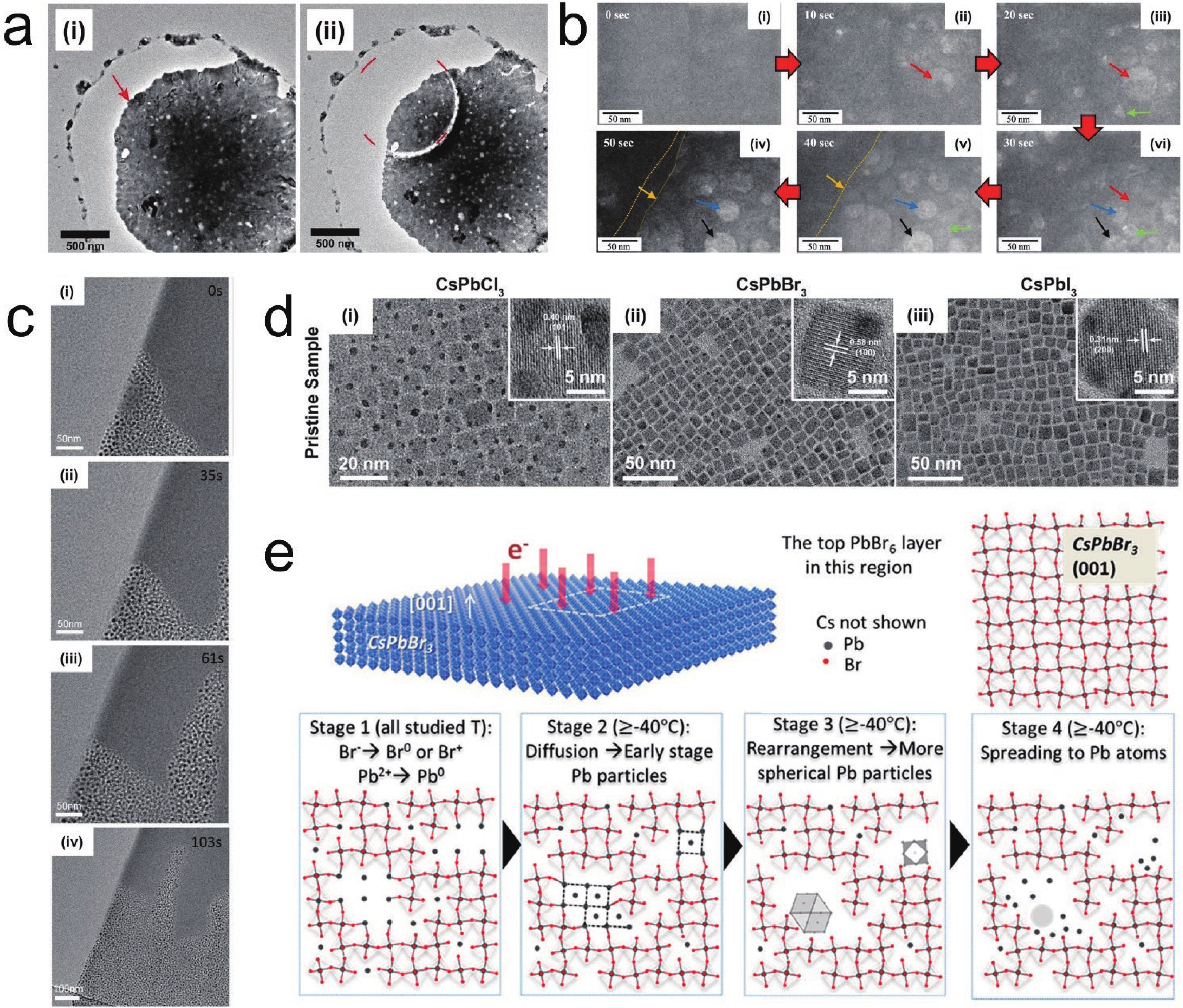
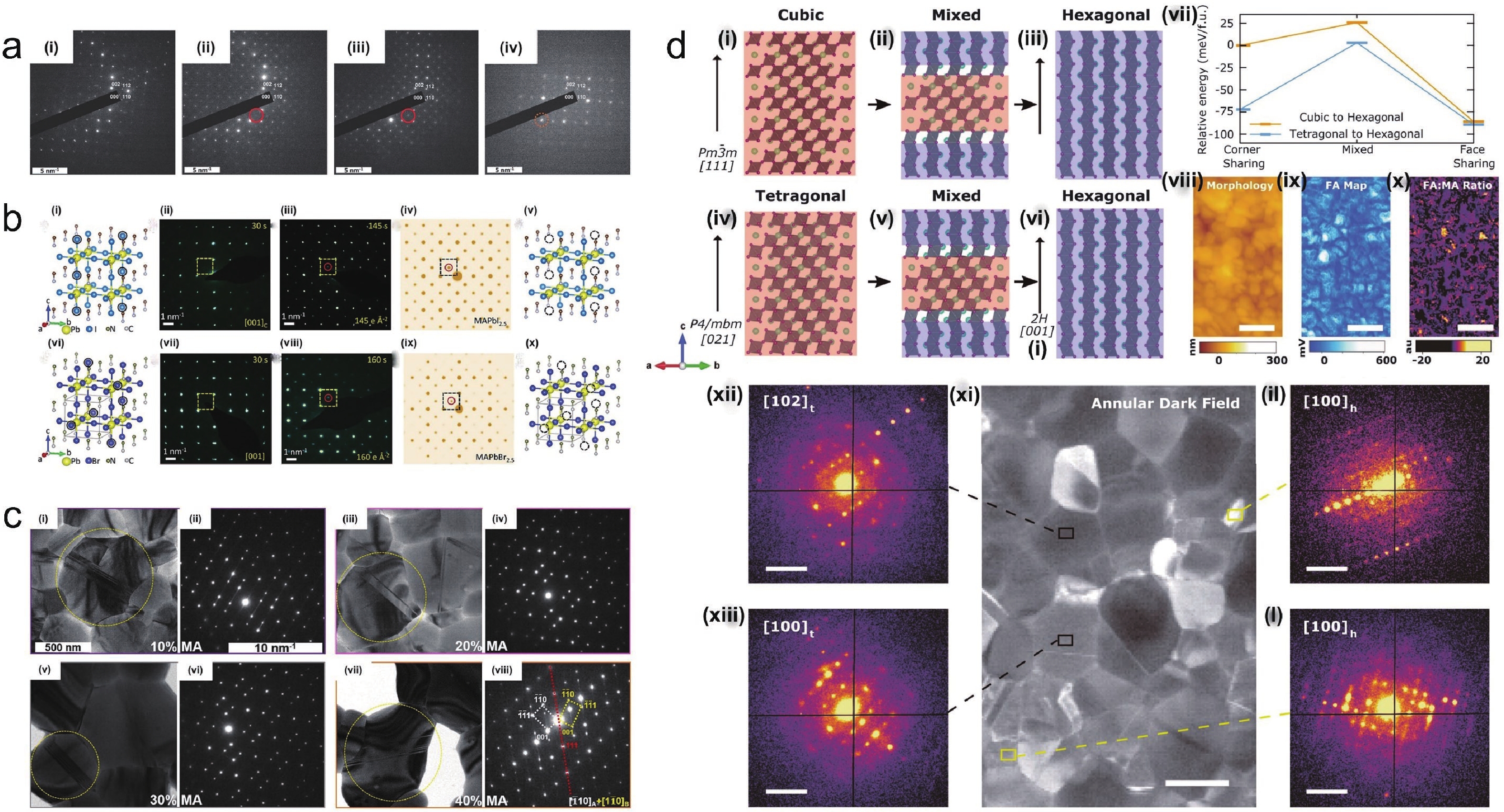
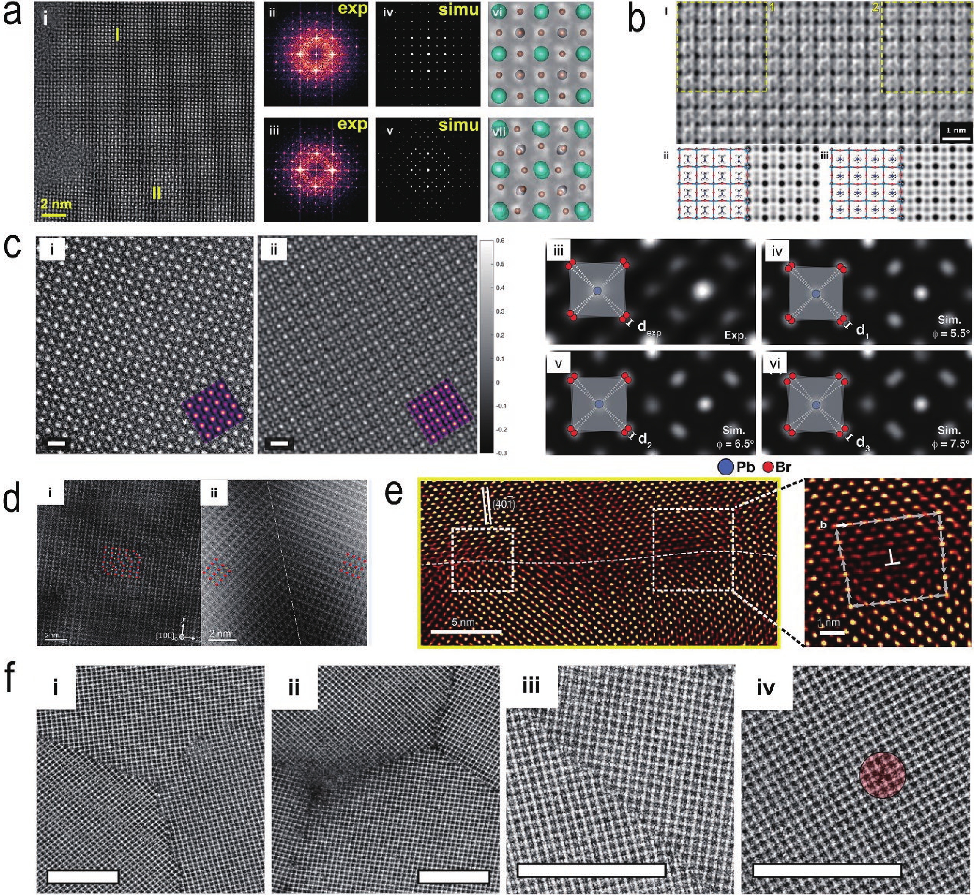
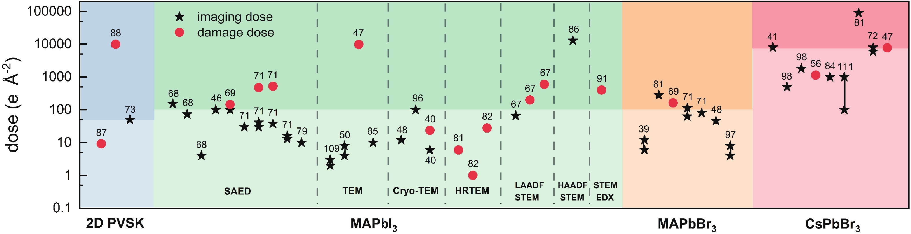
Table 1. Summary of TEM characterization details for MAPbI3 and related structures. No damage or little damage was reported unless specified in the table.
| Perovskite chemistry | Specimen morphology | TEM method | Special characterization tools | Accelerating voltage | Dose (e/Å2) | Dose rate (e/ (Å2·s)) | Damage evaluation and additional note | Corresponding figure in this review | Year and reference |
| MAPbI3 | Freestanding thin film | SAED | 200 | 1 | 2017, [38] | ||||
| MAPbI3 | Single crystal | SAED | 300 | 151 | 0.5 | Upper dose limit at mentioned dose rate before damage | 2018, [68] | ||
| 73 | 1 | ||||||||
| 4 | 2 | ||||||||
| MAPbI3 | Freestanding thin film | SAED | 200 | <100 | 2 | Exposure > 60 s at the mentioned dose rate led to damage | 3(a) | 2018, [46] | |
| MAPbI3 | Single crystal | SAED | 300 | <99 | 1 | Ordered vacancy was noticed at 145 e/(Å2·s) | 3(b) | 2020, [69] | |
| MAPbI3 | Single crystal | SAED | Cryogenic temperature | 300 | <30 | 2020, [71] | |||
| 25 | 300 | 30–41 | Damaged at the dose of 475 e/(Å2·s) | ||||||
| 90 | 300 | 38 | Damaged at the dose of 523 e/(Å2·s) | ||||||
| 80 | 13–16 | ||||||||
| MA/FAPbI3 | Freestanding thin film | SAED | 200 | 2 | 2021, [74] | ||||
| MAPbI3 | Single crystal | TEM | 200 | 4–8 | 1 | 2019, [50] | |||
| MAPbI3 | Freestanding thin film | TEM | 200 | 9870 | Damaged | 2(a) | 2019, [47] | ||
| MAPbI3 | Nanoparticles | TEM | Pulsed-beam TEM | 200 | 10 | 0.001 | 2020, [85] | ||
| MAPbI3/ FAPbI3 | Freestanding thin film | LAADF-STEM | 200 | 66 | Undamaged | 4(f) | 2020, [67] | ||
| 200 | Change in structure was noticed | ||||||||
| 600 | Damaged | ||||||||
| MAPbI3 | Nanowire | HRTEM | Cryo-TEM | 300 | 12 | 2019, [48] | |||
| MAPbI3 | Nanoparticles | HRTEM | Cryo-TEM | 300 | <100 | 6(a) | 2020, [96] | ||
| MAPbI3 | Nanoplatelets | HRTEM | Cryo-TEM | 300 | 5.96 | 2 | Lattice changed noticed at accumulated dose of 23.64 e/Å2 | 6(b) | 2021, [40] |
| MAPbI3 | – | HRTEM | Direct electron detector | 300 | 5.95 | Superstructure was noticed | 2021, [81] | ||
| MAPbI3 | Single crystal | HRTEM | Direct electron detector | 300 | 1 | MA loss at the mentioned dose | 2021, [82] | ||
| 300 | <28 | MA loss reached a balanced state between ~10.5 and 28.0 e/Å2 | |||||||
| MAPbI3 | FIB-milled PSC cross section | HAADF-STEM and STEM-EDX | In-situ heating ~150°C | 200 | 7(a) | 2016, [42] | |||
| MAPbI3 | FIB-milled PSC cross section | HAADF-STEM, STEM-EDX | In-situ biasing | 300 | Beam current of 50 pA was used | 2016, [108] | |||
| MAPbI3 | Nanoparticles | TEM | Liquid cell | 200 | <90 | Dose rate of >125 e/(Å2·s) causes damage | 2016, [113] | ||
| MAPbI3 | FIB-milled PSC cross section | TEM | In-situ biasing | 300 | 2–3 | 1–10 | 7(b) | 2018, [109] | |
| MAPbI3 | Nanoparticles | TEM | In-situ humidity | 200 | 1.3 | 7(c) | 2021, [112] | ||
| FA1−xCsxPbI3 FA0.5Cs0.5PbI3 | FIB-milled PSC cross section | HAADF-STEM | 300 | 1.3 × 10⁴ | A thin conformal coating of amorphous carbon about 10 nm thick was deposited to avoid beam damage | 4(d) | 2022, [86] | ||
| Cs0.05FA0.78 MA0.17Pb (I0.83Br0.17)3 | Nanoparticles | Scanning electron diffraction | 200 | 10 | 3(d) | 2021, [79] | |||
| Cs0.06FA0.79 MA0.15Pb (I0.85Br0.15)3 | FIB-milled PSC cross section | STEM-EDX | NA | >400 | Damaged | 2021, [91] |
 DownLoad: CSV
Table 2. Summary of TEM characterization details for MAPbBr3. No damage or little damage was reported unless specified in the table.
| Perovskite chemistry | Specimen morphology | TEM method | Special characteri- zation tool | Accelerating voltage | Dose (e/Å2) | Dose rate (e/(Å2·s)) | Damage evaluation and additional note | Corresponding figure in this review | Year and reference |
| MAPbBr3 | Single crystal | HRTEM | Direct electron detector | 300 | 6–12 | 4(b) | 2018, [39] | ||
| MAPbBr3 | – | HRTEM | iDPC | 300 | 280 | 2020, [81] | |||
| MAPbBr3 | Single crystal | SAED | 300 | 163 | <1 | Formation of ordered vacancy | 3(b) | 2020, [69] | |
| 300 | 63–113 | <1 | 2020, [71] | ||||||
| Cryogenic temperature | 300 | 81 | <1 | ||||||
| MAPbBr3 | Nanowire | HRTEM | Cryo-TEM | 46 | 2019, [48] | ||||
| MAPbBr3 | Nanoplatelets | HRTEM | Cryo-TEM | 300 | 4–8 | 4 | 2021, [97] |
DownLoad: CSV
Table 3. Summary of TEM characterization details for all-inorganic CsPbBr3 and related structures. No damage or little damage was reported unless specified in the table.
| Perovskite chemistry | Specimen morphology | TEM method | Special characteri- zation tool | Accelerating voltage | Dose (e/Å2) | Dose rate (e/(Å2·s)) | Damage evaluation and additional note | Corresponding figure in this review | Year and reference |
| CsPbBr3 | Nanosheets | HRTEM | In-line holography, imaging series | 80 | ~8000 | 100 | 4(a) | 2016, [41] | |
| Single frame acquisition | 80 | 3800 | |||||||
| CsPbBr3 | Nanosheets | HRTEM | <–40 ºC | 200 | 500 | 2017, [98] | |||
| HAADF-STEM | < –40 ºC | 200 | <1800 | ||||||
| CsPbBr3 | Nanosheets | HRTEM | 200 | 1140 | Pb formation | 2017, [56] | |||
| CsPbBr3 | Nanosheets | CBED | Cryogenic temperature | 200 | 4(c) | 2018, [84] | |||
| Ptycho graphy | Direct electron detector | 300 | 1000 | ||||||
| CsPbBr3 | Nanoparticles | TEM | 200 | 100–1000 | 2020, [111] | ||||
| CsPbBr3 | Nanosheets | EELS | 60 | The beam current was set to <5 pA | 2020, [93] | ||||
| CsPbBr3 | Nanoparticles | STEM-EDX | 300 | 9×10⁴ | Cyanamide passivation to protect surface from damage | 5(a)/5(b) | 2020, [81] 2021, [92] | ||
| CsPb (Br0.8I0.2)3 | Nanoparticles | HRTEM | 0 | 500 | Damaged | 2020, [59] | |||
| γ-CsPbIBr2 | Nanoparticles | HAADF-STEM | 300 | 6000–8000 | 2021, [72] | ||||
| CsPbI3 | Freestanding thin film | TEM | 200 | 7800 | Damaged | 2019, [47] |
DownLoad: CSV
Table 4. Summary of TEM characterization details for 2D halide perovskites. No damage or little damage was reported unless specified in the table.
| Perovskite chemistry | Specimen morphology | TEM method | Special characteri- zation tool | Accelerating voltage | Dose (e/Å2) | Dose rate (e/(Å2·s)) | Damage evaluation and additional note | Corresponding figure in this review | Year and reference |
| (2T)2PbI4– (2T)2PbBr4 | Nanosheets | HRTEM | 80 | 9.2 | 65 | Imaging series of 40 ms/frame. Damaged within 1 s | 4(e) | 2020, [87] | |
| BA2MA2Pb3I10 (n = 3) | Nanosheets | HRTEM | Direct electron detector | 300 | >104 | Surface damaged with reconstruction | 2019, [88] | ||
| BA2PbBr4 | Nanosheets | SAED | 300 | <1 | <1 (spot size 6) | 2(c) | 2019, [53] | ||
| BA2FAPb2I7/ BA2MAPb2I7 | Nanosheets | HRTEM | 200 | <50 | 2020, [73] |
DownLoad: CSV
| [1] |
Jiang Q, Zhao Y, Zhang X W, et al. Surface passivation of perovskite film for efficient solar cells. Nat Photonics, 2019, 13, 460 doi: 10.1038/s41566-019-0398-2
|
| [2] |
Lin Y W, Lin G M, Sun B Y, et al. Nanocrystalline perovskite hybrid photodetectors with high performance in almost every figure of merit. Adv Funct Mater, 2018, 28, 1705589 doi: 10.1002/adfm.201705589
|
| [3] |
Ran J H, Dyck O, Wang X Z, et al. Electron-beam-related studies of halide perovskites: Challenges and opportunities. Adv Energy Mater, 2020, 10, 1903191 doi: 10.1002/aenm.201903191
|
| [4] |
Chen P F, Ong W J, Shi Z H, et al. Pb-based halide perovskites: Recent advances in photo(electro)catalytic applications and looking beyond. Adv Funct Mater, 2020, 30, 1909667 doi: 10.1002/adfm.201909667
|
| [5] |
Ye T, Pan L, Yang Y, et al. Synthesis of highly-oriented black CsPbI3 microstructures for high-performance solar cells. Chem Mater, 2020, 32, 3235 doi: 10.1021/acs.chemmater.0c00427
|
| [6] |
Green M A, Ho-Baillie A, Snaith H J. The emergence of perovskite solar cells. Nat Photonics, 2014, 8, 506 doi: 10.1038/nphoton.2014.134
|
| [7] |
Dong Q, Fang Y, Shao Y, et al. Electron-hole diffusion lengths > 175 μm in solution-grown CH3NH3PbI3 single crystals. Science, 2015, 347, 967 doi: 10.1126/science.aaa5760
|
| [8] |
Shi Z J, Guo J, Chen Y H, et al. Lead-free organic-inorganic hybrid perovskites for photovoltaic applications: Recent advances and perspectives. Adv Mater, 2017, 29, 1605005 doi: 10.1002/adma.201605005
|
| [9] |
Yang Z B, Rajagopal A, Jen A K Y. Ideal bandgap organic–inorganic hybrid perovskite solar cells. Adv Mater, 2017, 29, 1704418 doi: 10.1002/adma.201704418
|
| [10] |
Kim M, Jeong J, Lu H Z, et al. Conformal quantum dot–SnO2 layers as electron transporters for efficient perovskite solar cells. Science, 2022, 375, 302 doi: 10.1126/science.abh1885
|
| [11] |
Liu C, Sun J, Tan W L, et al. Alkali cation doping for improving the structural stability of 2D perovskite in 3D/2D PSCs. Nano Lett, 2020, 20, 1240 doi: 10.1021/acs.nanolett.9b04661
|
| [12] |
Xie F X, Chen C C, Wu Y Z, et al. Vertical recrystallization for highly efficient and stable formamidinium-based inverted-structure perovskite solar cells. Energy Environ Sci, 2017, 10, 1942 doi: 10.1039/C7EE01675A
|
| [13] |
Xiang W C, Wang Z W, Kubicki D J, et al. Europium-doped CsPbI2Br for stable and highly efficient inorganic perovskite solar cells. Joule, 2019, 3, 205 doi: 10.1016/j.joule.2018.10.008
|
| [14] |
Yang S, Niu W X, Wang A L, et al. Ultrathin two-dimensional organic-inorganic hybrid perovskite nanosheets with bright, tunable photoluminescence and high stability. Angew Chem Int Ed, 2017, 56, 4252 doi: 10.1002/anie.201701134
|
| [15] |
Sun Y, Yin Y, Pols M, et al. Engineering the phases and heterostructures of ultrathin hybrid perovskite nanosheets. Adv Mater, 2020, 32, 2002392 doi: 10.1002/adma.202002392
|
| [16] |
Su Y, Chen X J, Ji W Y, et al. Highly controllable and efficient synthesis of mixed-halide CsPbX3 (X = Cl, Br, I) perovskite QDs toward the tunability of entire visible light. ACS Appl Mater Interfaces, 2017, 9, 33020 doi: 10.1021/acsami.7b10612
|
| [17] |
Utzat H, Sun W W, Kaplan A E K, et al. Coherent single-photon emission from colloidal lead halide perovskite quantum dots. Science, 2019, 363, 1068 doi: 10.1126/science.aau7392
|
| [18] |
Filip M R, Hillman S, Haghighirad A A, et al. Band gaps of the lead-free halide double perovskites Cs2BiAgCl6 and Cs2BiAgBr6 from theory and experiment. J Phys Chem Lett, 2016, 7, 2579 doi: 10.1021/acs.jpclett.6b01041
|
| [19] |
Zhong H X, Yang M, Tang G, et al. Type-II lateral heterostructures of monolayer halide double perovskites for optoelectronic applications. ACS Energy Lett, 2020, 5, 2275 doi: 10.1021/acsenergylett.0c01046
|
| [20] |
McClure E T, Ball M R, Windl W, et al. Cs2AgBiX6 (X = Br, Cl): New visible light absorbing, lead-free halide perovskite semiconductors. Chem Mater, 2016, 28, 1348 doi: 10.1021/acs.chemmater.5b04231
|
| [21] |
Wu C C, Zhang Q H, Liu Y, et al. The dawn of lead-free perovskite solar cell: Highly stable double perovskite Cs2AgBiBr6 film. Adv Sci, 2018, 5, 1700759 doi: 10.1002/advs.201700759
|
| [22] |
Volonakis G, Haghighirad A A, Milot R L, et al. Cs2InAgCl6: A new lead-free halide double perovskite with direct band gap. J Phys Chem Lett, 2017, 8, 772 doi: 10.1021/acs.jpclett.6b02682
|
| [23] |
Li Z Z, Yin W J. Recent progress in Pb-free stable inorganic double halide perovskites. J Semicond, 2018, 39, 071003 doi: 10.1088/1674-4926/39/7/071003
|
| [24] |
Xiao Z W, Yan Y F. Progress in theoretical study of metal halide perovskite solar cell materials. Adv Energy Mater, 2017, 7, 1701136 doi: 10.1002/aenm.201701136
|
| [25] |
Yang Y, Sun Y B, Jiang Y S. Structure and photocatalytic property of perovskite and perovskite-related compounds. Mater Chem Phys, 2006, 96, 234 doi: 10.1016/j.matchemphys.2005.07.007
|
| [26] |
Zhang H, Fu X, Tang Y, et al. Phase segregation due to ion migration in all-inorganic mixed-halide perovskite nanocrystals. Nat Commun, 2019, 10, 1088 doi: 10.1038/s41467-019-09047-7
|
| [27] |
Huang B Y, Liu Z H, Wu C W, et al. Polar or nonpolar? That is not the question for perovskite solar cells. Natl Sci Rev, 2021, 8, nwab094 doi: 10.1093/nsr/nwab094
|
| [28] |
Lei Y T, Xu Y K, Wang M, et al. Origin, influence, and countermeasures of defects in perovskite solar cells. Small, 2021, 17, 2005495 doi: 10.1002/smll.202005495
|
| [29] |
Wu J P, Liu S C, Li Z B, et al. Strain in perovskite solar cells: Origins, impacts and regulation. Natl Sci Rev, 2021, 8, nwab047 doi: 10.1093/nsr/nwab047
|
| [30] |
Sin C K, Zhang J Z, Tse K, et al. A brief review of formation energies calculation of surfaces and edges in semiconductors. J Semicond, 2020, 41, 061101 doi: 10.1088/1674-4926/41/6/061101
|
| [31] |
Bhattacharya S, Chandra G K, Predeep P. A microstructural analysis of 2D halide perovskites: Stability and functionality. Front Nanotechnol, 2021, 3, 657948 doi: 10.3389/fnano.2021.657948
|
| [32] |
Kim T W, Park N G. Methodologies for structural investigations of organic lead halide perovskites. Mater Today, 2020, 38, 67 doi: 10.1016/j.mattod.2020.03.025
|
| [33] |
Kumar V, Nisika, Kumar M. Temporal-spatial-energy resolved advance multidimensional techniques to probe photovoltaic materials from atomistic viewpoint for next-generation energy solutions. Energy Environ Sci, 2021, 14, 4760 doi: 10.1039/D1EE01165K
|
| [34] |
Liu J J. Advances and applications of atomic-resolution scanning transmission electron microscopy. Microsc Microan, 2021, 27, 943 doi: 10.1017/S1431927621012125
|
| [35] |
Ribet S M, Murthy A A, Roth E W, et al. Making the most of your electrons: Challenges and opportunities in characterizing hybrid interfaces with STEM. Mater Today, 2021, 50, 100 doi: 10.1016/j.mattod.2021.05.006
|
| [36] |
Zha F X, Zhang Q Y, Dai H G, et al. The scanning tunneling microscopy and spectroscopy of GaSb1– xBi x films of a few-nanometer thickness grown by molecular beam epitaxy. J Semicond, 2021, 42, 092101 doi: 10.1088/1674-4926/42/9/092101
|
| [37] |
Yang Z, Liu S Z. Perspective on the imaging device based on perovskite materials. J Semicond, 2020, 41, 050401 doi: 10.1088/1674-4926/41/5/050401
|
| [38] |
Rothmann M U, Li W, Zhu Y, et al. Direct observation of intrinsic twin domains in tetragonal CH3NH3PbI3. Nat Commun, 2017, 8, 14547 doi: 10.1038/ncomms14547
|
| [39] |
Zhang D L, Zhu Y H, Liu L M, et al. Atomic-resolution transmission electron microscopy of electron beam-sensitive crystalline materials. Science, 2018, 359, 675 doi: 10.1126/science.aao0865
|
| [40] |
Zhu Y, Wang S, Li B, et al. Twist-to-untwist evolution and cation polarization behavior of hybrid halide perovskite nanoplatelets revealed by cryogenic transmission electron microscopy. J Phys Chem Lett, 2021, 12, 12187-95 doi: 10.1021/acs.jpclett.1c03570
|
| [41] |
Yu Y, Zhang D D, Kisielowski C, et al. Atomic resolution imaging of halide perovskites. Nano Lett, 2016, 16, 7530 doi: 10.1021/acs.nanolett.6b03331
|
| [42] |
Divitini G, Cacovich S, Matteocci F, et al. In situ observation of heat-induced degradation of perovskite solar cells. Nat Energy, 2016, 1, 15012 doi: 10.1038/nenergy.2015.12
|
| [43] |
Seo Y H, Kim J H, Kim D H, et al. In situ TEM observation of the heat-induced degradation of single- and triple-cation planar perovskite solar cells. Nano Energy, 2020, 77, 105164 doi: 10.1016/j.nanoen.2020.105164
|
| [44] |
Ge Y, Mu X L, Lu Y, et al. Photoinduced degradation of lead halide perovskite thin films in air. Acta Phys Chim Sin, 2020, 36, 1905039 doi: 10.3866/PKU.WHXB201905039
|
| [45] |
Rothmann M U, Li W, Etheridge J, et al. Microstructural characterisations of perovskite solar cells - from grains to interfaces: Techniques, features, and challenges. Adv Energy Mater, 2017, 7, 1700912 doi: 10.1002/aenm.201700912
|
| [46] |
Rothmann M U, Li W, Zhu Y, et al. Structural and chemical changes to CH3NH3PbI3 induced by electron and gallium ion beams. Adv Mater, 2018, 30, 1800629 doi: 10.1002/adma.201800629
|
| [47] |
Chen X Y, Wang Z W. Investigating chemical and structural instabilities of lead halide perovskite induced by electron beam irradiation. Micron, 2019, 116, 73 doi: 10.1016/j.micron.2018.09.010
|
| [48] |
Li Y B, Zhou W J, Li Y Z, et al. Unravelling degradation mechanisms and atomic structure of organic-inorganic halide perovskites by cryo-EM. Joule, 2019, 3, 2854 doi: 10.1016/j.joule.2019.08.016
|
| [49] |
Kim T W, Kondo T. Direction-selective electron beam damage to CH3NH3PbI3 based on crystallographic anisotropy. Appl Phys Express, 2020, 13, 091001 doi: 10.35848/1882-0786/ababee
|
| [50] |
Alberti A, Bongiorno C, Smecca E, et al. Pb clustering and PbI2 nanofragmentation during methylammonium lead iodide perovskite degradation. Nat Commun, 2019, 10, 2196 doi: 10.1038/s41467-019-09909-0
|
| [51] |
Manekkathodi A, Marzouk A, Ponraj J, et al. Observation of structural phase transitions and PbI2 formation during the degradation of triple-cation double-halide perovskites. ACS Appl Energy Mater, 2020, 3, 6302 doi: 10.1021/acsaem.0c00515
|
| [52] |
Dou L T, Wong A B, Yu Y, et al. Atomically thin two-dimensional organic-inorganic hybrid perovskites. Science, 2015, 349, 1518 doi: 10.1126/science.aac7660
|
| [53] |
Nie L F, Ke X X, Sui M L. Microstructural study of two-dimensional organic-inorganic hybrid perovskite nanosheet degradation under illumination. Nanomaterials, 2019, 9, 722 doi: 10.3390/nano9050722
|
| [54] |
Li F, Liu Y, Wang H, et al. Postsynthetic surface trap removal of CsPbX3 (X = Cl, Br, or I) quantum dots via a ZnX2/hexane solution toward an enhanced luminescence quantum yield. Chem Mater, 2018, 30, 8546 doi: 10.1021/acs.chemmater.8b03442
|
| [55] |
Su G D, He B L, Gong Z K, et al. Enhanced charge extraction in carbon-based all-inorganic CsPbBr3 perovskite solar cells by dual-function interface engineering. Electrochim Acta, 2019, 328, 135102 doi: 10.1016/j.electacta.2019.135102
|
| [56] |
Dang Z Y, Shamsi J, Palazon F, et al. In situ transmission electron microscopy study of electron beam-induced transformations in colloidal cesium lead halide perovskite nanocrystals. ACS Nano, 2017, 11, 2124 doi: 10.1021/acsnano.6b08324
|
| [57] |
Zou S H, Liu C P, Li R F, et al. From nonluminescent to blue-emitting Cs4PbBr6 nanocrystals: Tailoring the insulator bandgap of 0D perovskite through Sn cation doping. Adv Mater, 2019, 31, 1900606 doi: 10.1002/adma.201900606
|
| [58] |
Wang T, Yang Z, Yang L, et al. Atomic-scale insights into the dynamics of growth and degradation of all-inorganic perovskite nanocrystals. J Phys Chem Lett, 2020, 11, 4618 doi: 10.1021/acs.jpclett.0c01220
|
| [59] |
Funk H, Shargaieva O, Eljarrat A, et al. In situ TEM monitoring of phase-segregation in inorganic mixed halide perovskite. J Phys Chem Lett, 2020, 11, 4945 doi: 10.1021/acs.jpclett.0c01296
|
| [60] |
Zhou W, Han P, Zhang X, et al. Lead-free small-bandgap Cs2CuSbCl6 double perovskite nanocrystals. J Phys Chem Lett, 2020, 11, 6463 doi: 10.1021/acs.jpclett.0c01968
|
| [61] |
Creutz S E, Crites E N, de Siena M C, et al. Colloidal nanocrystals of lead-free double-perovskite (elpasolite) semiconductors: Synthesis and anion exchange to access new materials. Nano Lett, 2018, 18, 1118 doi: 10.1021/acs.nanolett.7b04659
|
| [62] |
Feng Y H, Ke X X, Sui M L. Effect of electron irradiation on inorganic double perovskite solar cell material Cs2AgBiBr6. J Chin Electron Microsc Soc, 2020, 39, 1 doi: 10.3969/j.issn.1000-6281.2020.01.001
|
| [63] |
Egerton R F, Li P, Malac M. Radiation damage in the TEM and SEM. Micron, 2004, 35, 399 doi: 10.1016/j.micron.2004.02.003
|
| [64] |
Gong Z L, Yang Y. The application of synchrotron X-ray techniques to the study of rechargeable batteries. J Energy Chem, 2018, 27, 1566 doi: 10.1016/j.jechem.2018.03.020
|
| [65] |
Cai Z H, Wu Y N, Chen S Y. Energy-dependent knock-on damage of organic-inorganic hybrid perovskites under electron beam irradiation: First-principles insights. Appl Phys Lett, 2021, 119, 123901 doi: 10.1063/5.0065849
|
| [66] |
Chen Z X, Ke X X, Zhu L J, et al. Electron microscopy of organic-inorganic hybrid perovskite solar cell materials: degradation mechanism study and imaging condition optimization. J Chin Electron Microsc Soc, 2019, 38, 15 doi: 10.3969/j.issn.1000-6281.2019.01.003
|
| [67] |
Rothmann M U, Kim J S, Borchert J, et al. Atomic-scale microstructure of metal halide perovskite. Science, 2020, 370, 6516 doi: 10.1126/science.abb5940
|
| [68] |
Chen S, Zhang X, Zhao J, et al. Atomic scale insights into structure instability and decomposition pathway of methylammonium lead iodide perovskite. Nat Commun, 2018, 9, 4807 doi: 10.1038/s41467-018-07177-y
|
| [69] |
Chen S L, Zhang Y, Zhang X W, et al. General decomposition pathway of organic-inorganic hybrid perovskites through an intermediate superstructure and its suppression mechanism. Adv Mater, 2020, 32, 2001107 doi: 10.1002/adma.202001107
|
| [70] |
Chen S L, Gao P. Challenges, myths, and opportunities of electron microscopy on halide perovskites. J Appl Phys, 2020, 128, 010901 doi: 10.1063/5.0012310
|
| [71] |
Chen S L, Zhang Y, Zhao J J, et al. Transmission electron microscopy of organic-inorganic hybrid perovskites: Myths and truths. Sci Bull, 2020, 65, 1643 doi: 10.1016/j.scib.2020.05.020
|
| [72] |
Zhou X G, Yang C Q, Sang X, et al. Probing the electron beam-induced structural evolution of halide perovskite thin films by scanning transmission electron microscopy. J Phys Chem C, 2021, 125, 10786 doi: 10.1021/acs.jpcc.1c02156
|
| [73] |
Yuan B, Shi E Z, Liang C, et al. Structural damage of two-dimensional organic–inorganic halide perovskites. Inorganics, 2020, 8, 13 doi: 10.3390/inorganics8020013
|
| [74] |
Li W, Rothmann M U, Zhu Y, et al. The critical role of composition-dependent intragrain planar defects in the performance of MA1– xFA xPbI3 perovskite solar cells. Nat Energy, 2021, 6, 624 doi: 10.1038/s41560-021-00830-9
|
| [75] |
Gao Y, Shi E, Deng S, et al. Molecular engineering of organic–inorganic hybrid perovskites quantum wells. Nat Chem, 2019, 11, 1151 doi: 10.1038/s41557-019-0354-2
|
| [76] |
Pan W, Wu H, Luo J, et al. Cs2AgBiBr6 single-crystal X-ray detectors with a low detection limit. Nat Photonics, 2017, 11, 726 doi: 10.1038/s41566-017-0012-4
|
| [77] |
Luo J, Wang X, Li S, et al. Efficient and stable emission of warm-white light from lead-free halide double perovskites. Nature, 2018, 563, 541 doi: 10.1038/s41586-018-0691-0
|
| [78] |
Pham H T, Yin Y T, Andersson G, et al. Unraveling the influence of CsCl/MACl on the formation of nanotwins, stacking faults and cubic supercell structure in FA-based perovskite solar cells. Nano Energy, 2021, 87, 106226 doi: 10.1016/j.nanoen.2021.106226
|
| [79] |
Doherty T A S, Nagane S, Kubicki D J, et al. Stabilized tilted-octahedra halide perovskites inhibit local formation of performance-limiting phases. Science, 2021, 374, 1598 doi: 10.1126/science.abl4890
|
| [80] |
Brennan M C, Kuno M, Rouvimov S. Crystal structure of individual CsPbBr3 perovskite nanocubes. Inorg Chem, 2019, 58, 1555 doi: 10.1021/acs.inorgchem.8b03078
|
| [81] |
Song K P, Liu L M, Zhang D L, et al. Atomic-resolution imaging of halide perovskites using electron microscopy. Adv Energy Mater, 2020, 10, 1904006 doi: 10.1002/aenm.201904006
|
| [82] |
Chen S, Wu C, Han B, et al. Atomic-scale imaging of CH3NH3PbI3 structure and its decomposition pathway. Nat Commun, 2021, 12, 5516 doi: 10.1038/s41467-021-25832-9
|
| [83] |
Qiao G Y, Guan D H, Yuan S, et al. Perovskite quantum dots encapsulated in a mesoporous metal-organic framework as synergistic photocathode materials. J Am Chem Soc, 2021, 143, 14253 doi: 10.1021/jacs.1c05907
|
| [84] |
dos Reis R, Yang H, Ophus C, et al. Determination of the structural phase and octahedral rotation angle in halide perovskites. Appl Phys Lett, 2018, 112, 071901 doi: 10.1063/1.5017537
|
| [85] |
VandenBussche E J, Clark C P, Holmes R J, et al. Mitigating damage to hybrid perovskites using pulsed-beam TEM. ACS Omega, 2020, 5, 31867 doi: 10.1021/acsomega.0c04711
|
| [86] |
Cai S H, Dai J, Shao Z P, et al. Atomically resolved electrically active intragrain interfaces in perovskite semiconductors. J Am Chem Soc, 2022, 144, 1910 doi: 10.1021/jacs.1c12235
|
| [87] |
Shi E, Yuan B, Shiring S B, et al. Two-dimensional halide perovskite lateral epitaxial heterostructures. Nature, 2020, 580, 614 doi: 10.1038/s41586-020-2219-7
|
| [88] |
Jung H J, Stompus C C, Kanatzidis M G, et al. Self-passivation of 2D ruddlesden–popper perovskite by polytypic surface PbI2 encapsulation. Nano Lett, 2019, 19, 6109 doi: 10.1021/acs.nanolett.9b02069
|
| [89] |
Yu Y, Zhang D D, Yang P D. Ruddlesden-popper phase in two-dimensional inorganic halide perovskites: A plausible model and the supporting observations. Nano Lett, 2017, 17, 5489 doi: 10.1021/acs.nanolett.7b02146
|
| [90] |
Dang Z Y, Dhanabalan B, Castelli A, et al. Temperature-driven transformation of CsPbBr3 nanoplatelets into mosaic nanotiles in solution through self-assembly. Nano Lett, 2020, 20, 1808 doi: 10.1021/acs.nanolett.9b05036
|
| [91] |
Kosasih F U, Cacovich S, Divitini G, et al. Nanometric chemical analysis of beam-sensitive materials: A case study of STEM-EDX on perovskite solar cells. Small Methods, 2021, 5, 2000835 doi: 10.1002/smtd.202000835
|
| [92] |
Liu J, Song K, Zheng X, et al. Cyanamide passivation enables robust elemental imaging of metal halide perovskites at atomic resolution. J Phys Chem Lett, 2021, 12, 10402 doi: 10.1021/acs.jpclett.1c02830
|
| [93] |
Brescia R, Toso S, Ramasse Q, et al. Bandgap determination from individual orthorhombic thin cesium lead bromide nanosheets by electron energy-loss spectroscopy. Nanoscale Horiz, 2020, 5, 1610 doi: 10.1039/D0NH00477D
|
| [94] |
Li Y B, Huang W, Li Y Z, et al. Opportunities for cryogenic electron microscopy in materials science and nanoscience. ACS Nano, 2020, 14, 9263 doi: 10.1021/acsnano.0c05020
|
| [95] |
Zhang Z W, Cui Y, Vila R, et al. Cryogenic electron microscopy for energy materials. Acc Chem Res, 2021, 54, 3505 doi: 10.1021/acs.accounts.1c00183
|
| [96] |
Zhu Y M, Gui Z G, Wang Q, et al. Direct atomic scale characterization of the surface structure and planar defects in the organic-inorganic hybrid CH3NH3PbI3 by Cryo-TEM. Nano Energy, 2020, 73, 104820 doi: 10.1016/j.nanoen.2020.104820
|
| [97] |
Zhu Y M, Zhang Q, Yang X M, et al. Probing atomic structure of beam-sensitive energy materials in their native states using cryogenic transmission electron microscopes. iScience, 2021, 24, 103385 doi: 10.1016/j.isci.2021.103385
|
| [98] |
Dang Z Y, Shamsi J, Akkerman Q A, et al. Low-temperature electron beam-induced transformations of cesium lead halide perovskite nanocrystals. ACS Omega, 2017, 2, 5660 doi: 10.1021/acsomega.7b01009
|
| [99] |
Rivas N A, Babayigit A, Conings B, et al. Cryo-focused ion beam preparation of perovskite based solar cells for atom probe tomography. PLoS One, 2020, 15, e0227920 doi: 10.1371/journal.pone.0227920
|
| [100] |
Zhou J F, Wei N N, Zhang D L, et al. Cryogenic focused ion beam enables atomic-resolution imaging of local structures in highly sensitive bulk crystals and devices. J Am Chem Soc, 2022, 144, 3182 doi: 10.1021/jacs.1c12794
|
| [101] |
Lee J W, Seo S, Nandi P, et al. Dynamic structural property of organic-inorganic metal halide perovskite. iScience, 2021, 24, 101959 doi: 10.1016/j.isci.2020.101959
|
| [102] |
Stranks S D. Multimodal microscopy characterization of halide perovskite semiconductors: Revealing a new world (dis)order. Matter, 2021, 4, 3852 doi: 10.1016/j.matt.2021.10.025
|
| [103] |
Thampy S, Xu W J, Hsu J W P. Metal oxide-induced instability and its mitigation in halide perovskite solar cells. J Phys Chem Lett, 2021, 12, 8495 doi: 10.1021/acs.jpclett.1c02371
|
| [104] |
Zhang C C, Yuan S, Lou Y H, et al. Physical fields manipulation for high-performance perovskite photovoltaics. Small, 2022, 2107556 doi: 10.1002/smll.202107556
|
| [105] |
Kosasih F U, Ducati C. Characterising degradation of perovskite solar cells through in situ and operando electron microscopy. Nano Energy, 2018, 47, 243 doi: 10.1016/j.nanoen.2018.02.055
|
| [106] |
Kundu S, Kelly T L. In situ studies of the degradation mechanisms of perovskite solar cells. EcoMat, 2020, 2, e12025 doi: 10.1002/eom2.12025
|
| [107] |
McGrath F, Ghorpade U V, Ryan K M. Synthesis and dimensional control of CsPbBr3 perovskite nanocrystals using phosphorous based ligands. J Chem Phys, 2020, 152, 174702 doi: 10.1063/1.5128233
|
| [108] |
Jeangros Q, Duchamp M, Werner J, et al. In situ TEM analysis of organic-inorganic metal-halide perovskite solar cells under electrical bias. Nano Lett, 2016, 16, 7013 doi: 10.1021/acs.nanolett.6b03158
|
| [109] |
Jung H J, Kim D, Kim S, et al. Stability of halide perovskite solar cell devices: in situ observation of oxygen diffusion under biasing. Adv Mater, 2018, 30, 1802769 doi: 10.1002/adma.201802769
|
| [110] |
Kim M C, Ahn N, Cheng D Y, et al. Imaging real-time amorphization of hybrid perovskite solar cells under electrical biasing. ACS Energy Lett, 2021, 6, 3530 doi: 10.1021/acsenergylett.1c01707
|
| [111] |
Zhang C, Fernando J F S, Firestein K L, et al. Crystallography-derived optoelectronic and photovoltaic properties of CsPbBr3 perovskite single crystals as revealed by in situ transmission electron microscopy. Appl Mater Today, 2020, 20, 100788 doi: 10.1016/j.apmt.2020.100788
|
| [112] |
Akhavan Kazemi M A, Raval P, Cherednichekno K, et al. Molecular-level insight into correlation between surface defects and stability of methylammonium lead halide perovskite under controlled humidity. Small Methods, 2021, 5, 2000834 doi: 10.1002/smtd.202000834
|
| [113] |
Qin F Y, Wang Z W, Wang Z L. Anomalous growth and coalescence dynamics of hybrid perovskite nanoparticles observed by liquid-cell transmission electron microscopy. ACS Nano, 2016, 10, 9787 doi: 10.1021/acsnano.6b04234
|


Article views: 6288 Times PDF downloads: 522 Times Cited by: 0 Times
Received: 28 February 2022 Revised: 25 March 2022 Online: Accepted Manuscript: 06 April 2022Uncorrected proof: 12 April 2022Published: 18 April 2022
| Citation: |
Xiaomei Wu, Xiaoxing Ke, Manling Sui. Recent progress on advanced transmission electron microscopy characterization for halide perovskite semiconductors[J]. Journal of Semiconductors, 2022, 43(4): 041106. doi: 10.1088/1674-4926/43/4/041106
****
X M Wu, X X Ke, M L Sui. Recent progress on advanced transmission electron microscopy characterization for halide perovskite semiconductors[J]. J. Semicond, 2022, 43(4): 041106. doi: 10.1088/1674-4926/43/4/041106

|
| [1] |
Jiang Q, Zhao Y, Zhang X W, et al. Surface passivation of perovskite film for efficient solar cells. Nat Photonics, 2019, 13, 460 doi: 10.1038/s41566-019-0398-2
|
| [2] |
Lin Y W, Lin G M, Sun B Y, et al. Nanocrystalline perovskite hybrid photodetectors with high performance in almost every figure of merit. Adv Funct Mater, 2018, 28, 1705589 doi: 10.1002/adfm.201705589
|
| [3] |
Ran J H, Dyck O, Wang X Z, et al. Electron-beam-related studies of halide perovskites: Challenges and opportunities. Adv Energy Mater, 2020, 10, 1903191 doi: 10.1002/aenm.201903191
|
| [4] |
Chen P F, Ong W J, Shi Z H, et al. Pb-based halide perovskites: Recent advances in photo(electro)catalytic applications and looking beyond. Adv Funct Mater, 2020, 30, 1909667 doi: 10.1002/adfm.201909667
|
| [5] |
Ye T, Pan L, Yang Y, et al. Synthesis of highly-oriented black CsPbI3 microstructures for high-performance solar cells. Chem Mater, 2020, 32, 3235 doi: 10.1021/acs.chemmater.0c00427
|
| [6] |
Green M A, Ho-Baillie A, Snaith H J. The emergence of perovskite solar cells. Nat Photonics, 2014, 8, 506 doi: 10.1038/nphoton.2014.134
|
| [7] |
Dong Q, Fang Y, Shao Y, et al. Electron-hole diffusion lengths > 175 μm in solution-grown CH3NH3PbI3 single crystals. Science, 2015, 347, 967 doi: 10.1126/science.aaa5760
|
| [8] |
Shi Z J, Guo J, Chen Y H, et al. Lead-free organic-inorganic hybrid perovskites for photovoltaic applications: Recent advances and perspectives. Adv Mater, 2017, 29, 1605005 doi: 10.1002/adma.201605005
|
| [9] |
Yang Z B, Rajagopal A, Jen A K Y. Ideal bandgap organic–inorganic hybrid perovskite solar cells. Adv Mater, 2017, 29, 1704418 doi: 10.1002/adma.201704418
|
| [10] |
Kim M, Jeong J, Lu H Z, et al. Conformal quantum dot–SnO2 layers as electron transporters for efficient perovskite solar cells. Science, 2022, 375, 302 doi: 10.1126/science.abh1885
|
| [11] |
Liu C, Sun J, Tan W L, et al. Alkali cation doping for improving the structural stability of 2D perovskite in 3D/2D PSCs. Nano Lett, 2020, 20, 1240 doi: 10.1021/acs.nanolett.9b04661
|
| [12] |
Xie F X, Chen C C, Wu Y Z, et al. Vertical recrystallization for highly efficient and stable formamidinium-based inverted-structure perovskite solar cells. Energy Environ Sci, 2017, 10, 1942 doi: 10.1039/C7EE01675A
|
| [13] |
Xiang W C, Wang Z W, Kubicki D J, et al. Europium-doped CsPbI2Br for stable and highly efficient inorganic perovskite solar cells. Joule, 2019, 3, 205 doi: 10.1016/j.joule.2018.10.008
|
| [14] |
Yang S, Niu W X, Wang A L, et al. Ultrathin two-dimensional organic-inorganic hybrid perovskite nanosheets with bright, tunable photoluminescence and high stability. Angew Chem Int Ed, 2017, 56, 4252 doi: 10.1002/anie.201701134
|
| [15] |
Sun Y, Yin Y, Pols M, et al. Engineering the phases and heterostructures of ultrathin hybrid perovskite nanosheets. Adv Mater, 2020, 32, 2002392 doi: 10.1002/adma.202002392
|
| [16] |
Su Y, Chen X J, Ji W Y, et al. Highly controllable and efficient synthesis of mixed-halide CsPbX3 (X = Cl, Br, I) perovskite QDs toward the tunability of entire visible light. ACS Appl Mater Interfaces, 2017, 9, 33020 doi: 10.1021/acsami.7b10612
|
| [17] |
Utzat H, Sun W W, Kaplan A E K, et al. Coherent single-photon emission from colloidal lead halide perovskite quantum dots. Science, 2019, 363, 1068 doi: 10.1126/science.aau7392
|
| [18] |
Filip M R, Hillman S, Haghighirad A A, et al. Band gaps of the lead-free halide double perovskites Cs2BiAgCl6 and Cs2BiAgBr6 from theory and experiment. J Phys Chem Lett, 2016, 7, 2579 doi: 10.1021/acs.jpclett.6b01041
|
| [19] |
Zhong H X, Yang M, Tang G, et al. Type-II lateral heterostructures of monolayer halide double perovskites for optoelectronic applications. ACS Energy Lett, 2020, 5, 2275 doi: 10.1021/acsenergylett.0c01046
|
| [20] |
McClure E T, Ball M R, Windl W, et al. Cs2AgBiX6 (X = Br, Cl): New visible light absorbing, lead-free halide perovskite semiconductors. Chem Mater, 2016, 28, 1348 doi: 10.1021/acs.chemmater.5b04231
|
| [21] |
Wu C C, Zhang Q H, Liu Y, et al. The dawn of lead-free perovskite solar cell: Highly stable double perovskite Cs2AgBiBr6 film. Adv Sci, 2018, 5, 1700759 doi: 10.1002/advs.201700759
|
| [22] |
Volonakis G, Haghighirad A A, Milot R L, et al. Cs2InAgCl6: A new lead-free halide double perovskite with direct band gap. J Phys Chem Lett, 2017, 8, 772 doi: 10.1021/acs.jpclett.6b02682
|
| [23] |
Li Z Z, Yin W J. Recent progress in Pb-free stable inorganic double halide perovskites. J Semicond, 2018, 39, 071003 doi: 10.1088/1674-4926/39/7/071003
|
| [24] |
Xiao Z W, Yan Y F. Progress in theoretical study of metal halide perovskite solar cell materials. Adv Energy Mater, 2017, 7, 1701136 doi: 10.1002/aenm.201701136
|
| [25] |
Yang Y, Sun Y B, Jiang Y S. Structure and photocatalytic property of perovskite and perovskite-related compounds. Mater Chem Phys, 2006, 96, 234 doi: 10.1016/j.matchemphys.2005.07.007
|
| [26] |
Zhang H, Fu X, Tang Y, et al. Phase segregation due to ion migration in all-inorganic mixed-halide perovskite nanocrystals. Nat Commun, 2019, 10, 1088 doi: 10.1038/s41467-019-09047-7
|
| [27] |
Huang B Y, Liu Z H, Wu C W, et al. Polar or nonpolar? That is not the question for perovskite solar cells. Natl Sci Rev, 2021, 8, nwab094 doi: 10.1093/nsr/nwab094
|
| [28] |
Lei Y T, Xu Y K, Wang M, et al. Origin, influence, and countermeasures of defects in perovskite solar cells. Small, 2021, 17, 2005495 doi: 10.1002/smll.202005495
|
| [29] |
Wu J P, Liu S C, Li Z B, et al. Strain in perovskite solar cells: Origins, impacts and regulation. Natl Sci Rev, 2021, 8, nwab047 doi: 10.1093/nsr/nwab047
|
| [30] |
Sin C K, Zhang J Z, Tse K, et al. A brief review of formation energies calculation of surfaces and edges in semiconductors. J Semicond, 2020, 41, 061101 doi: 10.1088/1674-4926/41/6/061101
|
| [31] |
Bhattacharya S, Chandra G K, Predeep P. A microstructural analysis of 2D halide perovskites: Stability and functionality. Front Nanotechnol, 2021, 3, 657948 doi: 10.3389/fnano.2021.657948
|
| [32] |
Kim T W, Park N G. Methodologies for structural investigations of organic lead halide perovskites. Mater Today, 2020, 38, 67 doi: 10.1016/j.mattod.2020.03.025
|
| [33] |
Kumar V, Nisika, Kumar M. Temporal-spatial-energy resolved advance multidimensional techniques to probe photovoltaic materials from atomistic viewpoint for next-generation energy solutions. Energy Environ Sci, 2021, 14, 4760 doi: 10.1039/D1EE01165K
|
| [34] |
Liu J J. Advances and applications of atomic-resolution scanning transmission electron microscopy. Microsc Microan, 2021, 27, 943 doi: 10.1017/S1431927621012125
|
| [35] |
Ribet S M, Murthy A A, Roth E W, et al. Making the most of your electrons: Challenges and opportunities in characterizing hybrid interfaces with STEM. Mater Today, 2021, 50, 100 doi: 10.1016/j.mattod.2021.05.006
|
| [36] |
Zha F X, Zhang Q Y, Dai H G, et al. The scanning tunneling microscopy and spectroscopy of GaSb1– xBi x films of a few-nanometer thickness grown by molecular beam epitaxy. J Semicond, 2021, 42, 092101 doi: 10.1088/1674-4926/42/9/092101
|
| [37] |
Yang Z, Liu S Z. Perspective on the imaging device based on perovskite materials. J Semicond, 2020, 41, 050401 doi: 10.1088/1674-4926/41/5/050401
|
| [38] |
Rothmann M U, Li W, Zhu Y, et al. Direct observation of intrinsic twin domains in tetragonal CH3NH3PbI3. Nat Commun, 2017, 8, 14547 doi: 10.1038/ncomms14547
|
| [39] |
Zhang D L, Zhu Y H, Liu L M, et al. Atomic-resolution transmission electron microscopy of electron beam-sensitive crystalline materials. Science, 2018, 359, 675 doi: 10.1126/science.aao0865
|
| [40] |
Zhu Y, Wang S, Li B, et al. Twist-to-untwist evolution and cation polarization behavior of hybrid halide perovskite nanoplatelets revealed by cryogenic transmission electron microscopy. J Phys Chem Lett, 2021, 12, 12187-95 doi: 10.1021/acs.jpclett.1c03570
|
| [41] |
Yu Y, Zhang D D, Kisielowski C, et al. Atomic resolution imaging of halide perovskites. Nano Lett, 2016, 16, 7530 doi: 10.1021/acs.nanolett.6b03331
|
| [42] |
Divitini G, Cacovich S, Matteocci F, et al. In situ observation of heat-induced degradation of perovskite solar cells. Nat Energy, 2016, 1, 15012 doi: 10.1038/nenergy.2015.12
|
| [43] |
Seo Y H, Kim J H, Kim D H, et al. In situ TEM observation of the heat-induced degradation of single- and triple-cation planar perovskite solar cells. Nano Energy, 2020, 77, 105164 doi: 10.1016/j.nanoen.2020.105164
|
| [44] |
Ge Y, Mu X L, Lu Y, et al. Photoinduced degradation of lead halide perovskite thin films in air. Acta Phys Chim Sin, 2020, 36, 1905039 doi: 10.3866/PKU.WHXB201905039
|
| [45] |
Rothmann M U, Li W, Etheridge J, et al. Microstructural characterisations of perovskite solar cells - from grains to interfaces: Techniques, features, and challenges. Adv Energy Mater, 2017, 7, 1700912 doi: 10.1002/aenm.201700912
|
| [46] |
Rothmann M U, Li W, Zhu Y, et al. Structural and chemical changes to CH3NH3PbI3 induced by electron and gallium ion beams. Adv Mater, 2018, 30, 1800629 doi: 10.1002/adma.201800629
|
| [47] |
Chen X Y, Wang Z W. Investigating chemical and structural instabilities of lead halide perovskite induced by electron beam irradiation. Micron, 2019, 116, 73 doi: 10.1016/j.micron.2018.09.010
|
| [48] |
Li Y B, Zhou W J, Li Y Z, et al. Unravelling degradation mechanisms and atomic structure of organic-inorganic halide perovskites by cryo-EM. Joule, 2019, 3, 2854 doi: 10.1016/j.joule.2019.08.016
|
| [49] |
Kim T W, Kondo T. Direction-selective electron beam damage to CH3NH3PbI3 based on crystallographic anisotropy. Appl Phys Express, 2020, 13, 091001 doi: 10.35848/1882-0786/ababee
|
| [50] |
Alberti A, Bongiorno C, Smecca E, et al. Pb clustering and PbI2 nanofragmentation during methylammonium lead iodide perovskite degradation. Nat Commun, 2019, 10, 2196 doi: 10.1038/s41467-019-09909-0
|
| [51] |
Manekkathodi A, Marzouk A, Ponraj J, et al. Observation of structural phase transitions and PbI2 formation during the degradation of triple-cation double-halide perovskites. ACS Appl Energy Mater, 2020, 3, 6302 doi: 10.1021/acsaem.0c00515
|
| [52] |
Dou L T, Wong A B, Yu Y, et al. Atomically thin two-dimensional organic-inorganic hybrid perovskites. Science, 2015, 349, 1518 doi: 10.1126/science.aac7660
|
| [53] |
Nie L F, Ke X X, Sui M L. Microstructural study of two-dimensional organic-inorganic hybrid perovskite nanosheet degradation under illumination. Nanomaterials, 2019, 9, 722 doi: 10.3390/nano9050722
|
| [54] |
Li F, Liu Y, Wang H, et al. Postsynthetic surface trap removal of CsPbX3 (X = Cl, Br, or I) quantum dots via a ZnX2/hexane solution toward an enhanced luminescence quantum yield. Chem Mater, 2018, 30, 8546 doi: 10.1021/acs.chemmater.8b03442
|
| [55] |
Su G D, He B L, Gong Z K, et al. Enhanced charge extraction in carbon-based all-inorganic CsPbBr3 perovskite solar cells by dual-function interface engineering. Electrochim Acta, 2019, 328, 135102 doi: 10.1016/j.electacta.2019.135102
|
| [56] |
Dang Z Y, Shamsi J, Palazon F, et al. In situ transmission electron microscopy study of electron beam-induced transformations in colloidal cesium lead halide perovskite nanocrystals. ACS Nano, 2017, 11, 2124 doi: 10.1021/acsnano.6b08324
|
| [57] |
Zou S H, Liu C P, Li R F, et al. From nonluminescent to blue-emitting Cs4PbBr6 nanocrystals: Tailoring the insulator bandgap of 0D perovskite through Sn cation doping. Adv Mater, 2019, 31, 1900606 doi: 10.1002/adma.201900606
|
| [58] |
Wang T, Yang Z, Yang L, et al. Atomic-scale insights into the dynamics of growth and degradation of all-inorganic perovskite nanocrystals. J Phys Chem Lett, 2020, 11, 4618 doi: 10.1021/acs.jpclett.0c01220
|
| [59] |
Funk H, Shargaieva O, Eljarrat A, et al. In situ TEM monitoring of phase-segregation in inorganic mixed halide perovskite. J Phys Chem Lett, 2020, 11, 4945 doi: 10.1021/acs.jpclett.0c01296
|
| [60] |
Zhou W, Han P, Zhang X, et al. Lead-free small-bandgap Cs2CuSbCl6 double perovskite nanocrystals. J Phys Chem Lett, 2020, 11, 6463 doi: 10.1021/acs.jpclett.0c01968
|
| [61] |
Creutz S E, Crites E N, de Siena M C, et al. Colloidal nanocrystals of lead-free double-perovskite (elpasolite) semiconductors: Synthesis and anion exchange to access new materials. Nano Lett, 2018, 18, 1118 doi: 10.1021/acs.nanolett.7b04659
|
| [62] |
Feng Y H, Ke X X, Sui M L. Effect of electron irradiation on inorganic double perovskite solar cell material Cs2AgBiBr6. J Chin Electron Microsc Soc, 2020, 39, 1 doi: 10.3969/j.issn.1000-6281.2020.01.001
|
| [63] |
Egerton R F, Li P, Malac M. Radiation damage in the TEM and SEM. Micron, 2004, 35, 399 doi: 10.1016/j.micron.2004.02.003
|
| [64] |
Gong Z L, Yang Y. The application of synchrotron X-ray techniques to the study of rechargeable batteries. J Energy Chem, 2018, 27, 1566 doi: 10.1016/j.jechem.2018.03.020
|
| [65] |
Cai Z H, Wu Y N, Chen S Y. Energy-dependent knock-on damage of organic-inorganic hybrid perovskites under electron beam irradiation: First-principles insights. Appl Phys Lett, 2021, 119, 123901 doi: 10.1063/5.0065849
|
| [66] |
Chen Z X, Ke X X, Zhu L J, et al. Electron microscopy of organic-inorganic hybrid perovskite solar cell materials: degradation mechanism study and imaging condition optimization. J Chin Electron Microsc Soc, 2019, 38, 15 doi: 10.3969/j.issn.1000-6281.2019.01.003
|
| [67] |
Rothmann M U, Kim J S, Borchert J, et al. Atomic-scale microstructure of metal halide perovskite. Science, 2020, 370, 6516 doi: 10.1126/science.abb5940
|
| [68] |
Chen S, Zhang X, Zhao J, et al. Atomic scale insights into structure instability and decomposition pathway of methylammonium lead iodide perovskite. Nat Commun, 2018, 9, 4807 doi: 10.1038/s41467-018-07177-y
|
| [69] |
Chen S L, Zhang Y, Zhang X W, et al. General decomposition pathway of organic-inorganic hybrid perovskites through an intermediate superstructure and its suppression mechanism. Adv Mater, 2020, 32, 2001107 doi: 10.1002/adma.202001107
|
| [70] |
Chen S L, Gao P. Challenges, myths, and opportunities of electron microscopy on halide perovskites. J Appl Phys, 2020, 128, 010901 doi: 10.1063/5.0012310
|
| [71] |
Chen S L, Zhang Y, Zhao J J, et al. Transmission electron microscopy of organic-inorganic hybrid perovskites: Myths and truths. Sci Bull, 2020, 65, 1643 doi: 10.1016/j.scib.2020.05.020
|
| [72] |
Zhou X G, Yang C Q, Sang X, et al. Probing the electron beam-induced structural evolution of halide perovskite thin films by scanning transmission electron microscopy. J Phys Chem C, 2021, 125, 10786 doi: 10.1021/acs.jpcc.1c02156
|
| [73] |
Yuan B, Shi E Z, Liang C, et al. Structural damage of two-dimensional organic–inorganic halide perovskites. Inorganics, 2020, 8, 13 doi: 10.3390/inorganics8020013
|
| [74] |
Li W, Rothmann M U, Zhu Y, et al. The critical role of composition-dependent intragrain planar defects in the performance of MA1– xFA xPbI3 perovskite solar cells. Nat Energy, 2021, 6, 624 doi: 10.1038/s41560-021-00830-9
|
| [75] |
Gao Y, Shi E, Deng S, et al. Molecular engineering of organic–inorganic hybrid perovskites quantum wells. Nat Chem, 2019, 11, 1151 doi: 10.1038/s41557-019-0354-2
|
| [76] |
Pan W, Wu H, Luo J, et al. Cs2AgBiBr6 single-crystal X-ray detectors with a low detection limit. Nat Photonics, 2017, 11, 726 doi: 10.1038/s41566-017-0012-4
|
| [77] |
Luo J, Wang X, Li S, et al. Efficient and stable emission of warm-white light from lead-free halide double perovskites. Nature, 2018, 563, 541 doi: 10.1038/s41586-018-0691-0
|
| [78] |
Pham H T, Yin Y T, Andersson G, et al. Unraveling the influence of CsCl/MACl on the formation of nanotwins, stacking faults and cubic supercell structure in FA-based perovskite solar cells. Nano Energy, 2021, 87, 106226 doi: 10.1016/j.nanoen.2021.106226
|
| [79] |
Doherty T A S, Nagane S, Kubicki D J, et al. Stabilized tilted-octahedra halide perovskites inhibit local formation of performance-limiting phases. Science, 2021, 374, 1598 doi: 10.1126/science.abl4890
|
| [80] |
Brennan M C, Kuno M, Rouvimov S. Crystal structure of individual CsPbBr3 perovskite nanocubes. Inorg Chem, 2019, 58, 1555 doi: 10.1021/acs.inorgchem.8b03078
|
| [81] |
Song K P, Liu L M, Zhang D L, et al. Atomic-resolution imaging of halide perovskites using electron microscopy. Adv Energy Mater, 2020, 10, 1904006 doi: 10.1002/aenm.201904006
|
| [82] |
Chen S, Wu C, Han B, et al. Atomic-scale imaging of CH3NH3PbI3 structure and its decomposition pathway. Nat Commun, 2021, 12, 5516 doi: 10.1038/s41467-021-25832-9
|
| [83] |
Qiao G Y, Guan D H, Yuan S, et al. Perovskite quantum dots encapsulated in a mesoporous metal-organic framework as synergistic photocathode materials. J Am Chem Soc, 2021, 143, 14253 doi: 10.1021/jacs.1c05907
|
| [84] |
dos Reis R, Yang H, Ophus C, et al. Determination of the structural phase and octahedral rotation angle in halide perovskites. Appl Phys Lett, 2018, 112, 071901 doi: 10.1063/1.5017537
|
| [85] |
VandenBussche E J, Clark C P, Holmes R J, et al. Mitigating damage to hybrid perovskites using pulsed-beam TEM. ACS Omega, 2020, 5, 31867 doi: 10.1021/acsomega.0c04711
|
| [86] |
Cai S H, Dai J, Shao Z P, et al. Atomically resolved electrically active intragrain interfaces in perovskite semiconductors. J Am Chem Soc, 2022, 144, 1910 doi: 10.1021/jacs.1c12235
|
| [87] |
Shi E, Yuan B, Shiring S B, et al. Two-dimensional halide perovskite lateral epitaxial heterostructures. Nature, 2020, 580, 614 doi: 10.1038/s41586-020-2219-7
|
| [88] |
Jung H J, Stompus C C, Kanatzidis M G, et al. Self-passivation of 2D ruddlesden–popper perovskite by polytypic surface PbI2 encapsulation. Nano Lett, 2019, 19, 6109 doi: 10.1021/acs.nanolett.9b02069
|
| [89] |
Yu Y, Zhang D D, Yang P D. Ruddlesden-popper phase in two-dimensional inorganic halide perovskites: A plausible model and the supporting observations. Nano Lett, 2017, 17, 5489 doi: 10.1021/acs.nanolett.7b02146
|
| [90] |
Dang Z Y, Dhanabalan B, Castelli A, et al. Temperature-driven transformation of CsPbBr3 nanoplatelets into mosaic nanotiles in solution through self-assembly. Nano Lett, 2020, 20, 1808 doi: 10.1021/acs.nanolett.9b05036
|
| [91] |
Kosasih F U, Cacovich S, Divitini G, et al. Nanometric chemical analysis of beam-sensitive materials: A case study of STEM-EDX on perovskite solar cells. Small Methods, 2021, 5, 2000835 doi: 10.1002/smtd.202000835
|
| [92] |
Liu J, Song K, Zheng X, et al. Cyanamide passivation enables robust elemental imaging of metal halide perovskites at atomic resolution. J Phys Chem Lett, 2021, 12, 10402 doi: 10.1021/acs.jpclett.1c02830
|
| [93] |
Brescia R, Toso S, Ramasse Q, et al. Bandgap determination from individual orthorhombic thin cesium lead bromide nanosheets by electron energy-loss spectroscopy. Nanoscale Horiz, 2020, 5, 1610 doi: 10.1039/D0NH00477D
|
| [94] |
Li Y B, Huang W, Li Y Z, et al. Opportunities for cryogenic electron microscopy in materials science and nanoscience. ACS Nano, 2020, 14, 9263 doi: 10.1021/acsnano.0c05020
|
| [95] |
Zhang Z W, Cui Y, Vila R, et al. Cryogenic electron microscopy for energy materials. Acc Chem Res, 2021, 54, 3505 doi: 10.1021/acs.accounts.1c00183
|
| [96] |
Zhu Y M, Gui Z G, Wang Q, et al. Direct atomic scale characterization of the surface structure and planar defects in the organic-inorganic hybrid CH3NH3PbI3 by Cryo-TEM. Nano Energy, 2020, 73, 104820 doi: 10.1016/j.nanoen.2020.104820
|
| [97] |
Zhu Y M, Zhang Q, Yang X M, et al. Probing atomic structure of beam-sensitive energy materials in their native states using cryogenic transmission electron microscopes. iScience, 2021, 24, 103385 doi: 10.1016/j.isci.2021.103385
|
| [98] |
Dang Z Y, Shamsi J, Akkerman Q A, et al. Low-temperature electron beam-induced transformations of cesium lead halide perovskite nanocrystals. ACS Omega, 2017, 2, 5660 doi: 10.1021/acsomega.7b01009
|
| [99] |
Rivas N A, Babayigit A, Conings B, et al. Cryo-focused ion beam preparation of perovskite based solar cells for atom probe tomography. PLoS One, 2020, 15, e0227920 doi: 10.1371/journal.pone.0227920
|
| [100] |
Zhou J F, Wei N N, Zhang D L, et al. Cryogenic focused ion beam enables atomic-resolution imaging of local structures in highly sensitive bulk crystals and devices. J Am Chem Soc, 2022, 144, 3182 doi: 10.1021/jacs.1c12794
|
| [101] |
Lee J W, Seo S, Nandi P, et al. Dynamic structural property of organic-inorganic metal halide perovskite. iScience, 2021, 24, 101959 doi: 10.1016/j.isci.2020.101959
|
| [102] |
Stranks S D. Multimodal microscopy characterization of halide perovskite semiconductors: Revealing a new world (dis)order. Matter, 2021, 4, 3852 doi: 10.1016/j.matt.2021.10.025
|
| [103] |
Thampy S, Xu W J, Hsu J W P. Metal oxide-induced instability and its mitigation in halide perovskite solar cells. J Phys Chem Lett, 2021, 12, 8495 doi: 10.1021/acs.jpclett.1c02371
|
| [104] |
Zhang C C, Yuan S, Lou Y H, et al. Physical fields manipulation for high-performance perovskite photovoltaics. Small, 2022, 2107556 doi: 10.1002/smll.202107556
|
| [105] |
Kosasih F U, Ducati C. Characterising degradation of perovskite solar cells through in situ and operando electron microscopy. Nano Energy, 2018, 47, 243 doi: 10.1016/j.nanoen.2018.02.055
|
| [106] |
Kundu S, Kelly T L. In situ studies of the degradation mechanisms of perovskite solar cells. EcoMat, 2020, 2, e12025 doi: 10.1002/eom2.12025
|
| [107] |
McGrath F, Ghorpade U V, Ryan K M. Synthesis and dimensional control of CsPbBr3 perovskite nanocrystals using phosphorous based ligands. J Chem Phys, 2020, 152, 174702 doi: 10.1063/1.5128233
|
| [108] |
Jeangros Q, Duchamp M, Werner J, et al. In situ TEM analysis of organic-inorganic metal-halide perovskite solar cells under electrical bias. Nano Lett, 2016, 16, 7013 doi: 10.1021/acs.nanolett.6b03158
|
| [109] |
Jung H J, Kim D, Kim S, et al. Stability of halide perovskite solar cell devices: in situ observation of oxygen diffusion under biasing. Adv Mater, 2018, 30, 1802769 doi: 10.1002/adma.201802769
|
| [110] |
Kim M C, Ahn N, Cheng D Y, et al. Imaging real-time amorphization of hybrid perovskite solar cells under electrical biasing. ACS Energy Lett, 2021, 6, 3530 doi: 10.1021/acsenergylett.1c01707
|
| [111] |
Zhang C, Fernando J F S, Firestein K L, et al. Crystallography-derived optoelectronic and photovoltaic properties of CsPbBr3 perovskite single crystals as revealed by in situ transmission electron microscopy. Appl Mater Today, 2020, 20, 100788 doi: 10.1016/j.apmt.2020.100788
|
| [112] |
Akhavan Kazemi M A, Raval P, Cherednichekno K, et al. Molecular-level insight into correlation between surface defects and stability of methylammonium lead halide perovskite under controlled humidity. Small Methods, 2021, 5, 2000834 doi: 10.1002/smtd.202000834
|
| [113] |
Qin F Y, Wang Z W, Wang Z L. Anomalous growth and coalescence dynamics of hybrid perovskite nanoparticles observed by liquid-cell transmission electron microscopy. ACS Nano, 2016, 10, 9787 doi: 10.1021/acsnano.6b04234
|

 WeChat ID
Journal of Semiconductors © 2017 All Rights Reserved 京ICP备05085259号-2


