


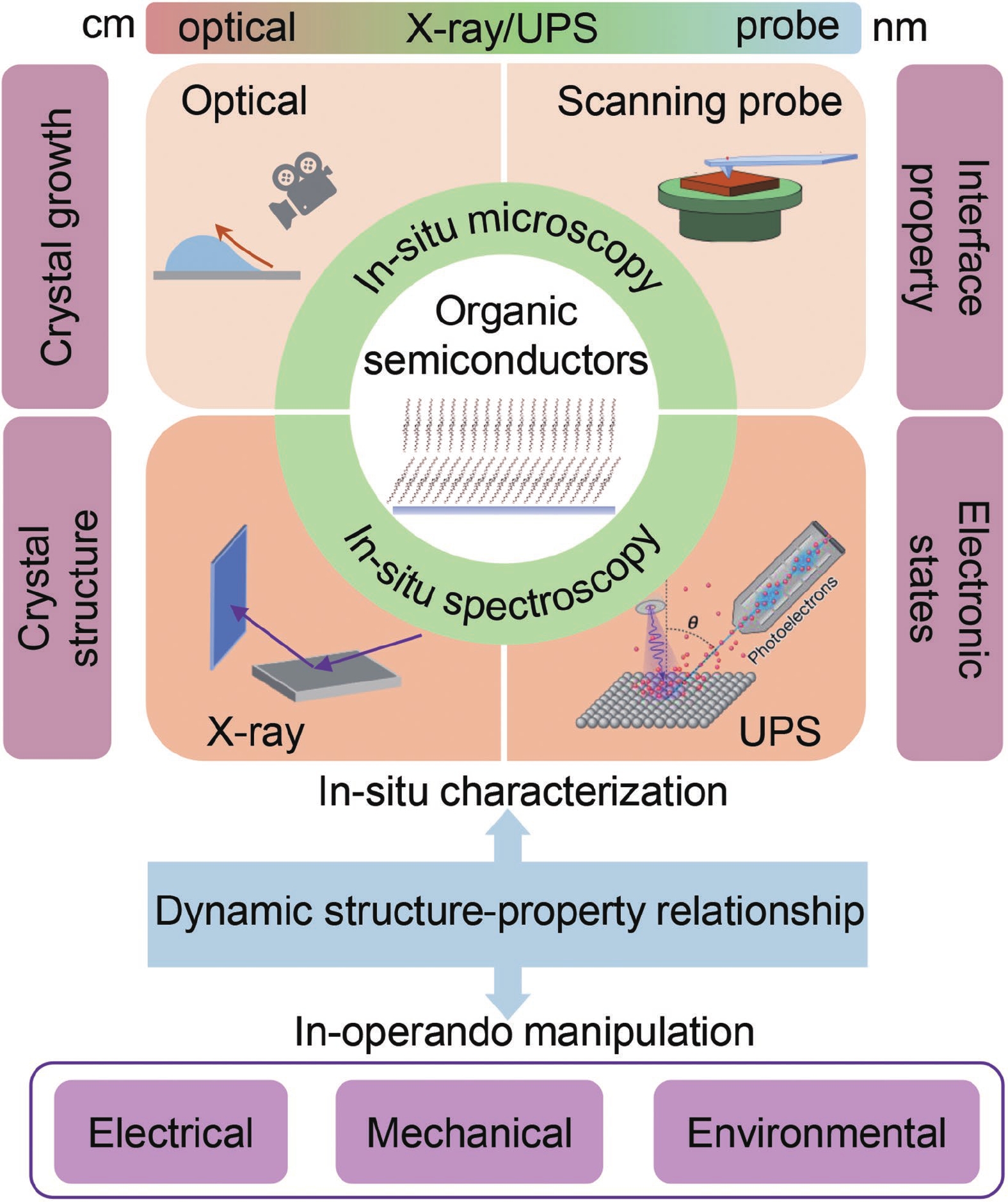
Fig. 1.
(Color online) Overview of various in-situ characterization techniques with different resolutions, from centimeter to nanometer, to study the dynamic structure-property relationship under manipulation.
REVIEWS
Sai Jiang1, , Qinyong Dai2, Jianhang Guo2 and Yun Li2,
Corresponding author: Sai Jiang, saijiang@cczu.edu.cn; Yun Li, yli@nju.edu.cn
Abstract: The increasing demands of multifunctional organic electronics require advanced organic semiconducting materials to be developed and significant improvements to be made to device performance. Thus, it is necessary to gain an in-depth understanding of the film growth process, electronic states, and dynamic structure-property relationship under realistic operation conditions, which can be obtained by in-situ/operando characterization techniques for organic devices. Here, the up-to-date developments in the in-situ/operando optical, scanning probe microscopy, and spectroscopy techniques that are employed for studies of film morphological evolution, crystal structures, semiconductor-electrolyte interface properties, and charge carrier dynamics are described and summarized. These advanced technologies leverage the traditional static characterizations into an in-situ and interactive manipulation of organic semiconducting films and devices without sacrificing the resolution, which facilitates the exploration of the intrinsic structure-property relationship of organic materials and the optimization of organic devices for advanced applications.
Keywords: in-situ/operando characterization, organic semiconductors, structure-property relationship
| [1] |
Tsumura A, Koezuka H, Ando T. Macromolecular electronic device: Field-effect transistor with a polythiophene thin film. Appl Phys Lett, 1986, 49, 1210 doi: 10.1063/1.97417
|
| [2] |
Li L Q, Gao P, Wang W C, et al. Growth of ultrathin organic semiconductor microstripes with thickness control in the monolayer precision. Angew Chem Int Ed, 2013, 52, 12530 doi: 10.1002/anie.201306953
|
| [3] |
Yuan Y B, Giri G, Ayzner A L, et al. Ultra-high mobility transparent organic thin film transistors grown by an off-centre spin-coating method. Nat Commun, 2014, 5, 3005 doi: 10.1038/ncomms4005
|
| [4] |
Zhang Y H, Qiao J S, Gao S, et al. Probing carrier transport and structure-property relationship of highly ordered organic semiconductors at the two-dimensional limit. Phys Rev Lett, 2016, 116, 016602 doi: 10.1103/PhysRevLett.116.016602
|
| [5] |
Lin P, Yan F. Organic thin-film transistors for chemical and biological sensing. Adv Mater, 2012, 24, 34 doi: 10.1002/adma.201103334
|
| [6] |
van de Burgt Y, Melianas A, Keene S T, et al. Organic electronics for neuromorphic computing. Nat Electron, 2018, 1, 386 doi: 10.1038/s41928-018-0103-3
|
| [7] |
Minemawari H, Yamada T, Matsui H, et al. Inkjet printing of single-crystal films. Nature, 2011, 475, 364 doi: 10.1038/nature10313
|
| [8] |
Wang C L, Dong H L, Jiang L, et al. Organic semiconductor crystals. Chem Soc Rev, 2018, 47, 422 doi: 10.1039/C7CS00490G
|
| [9] |
Wang Q J, Qian J, Li Y, et al. 2D single-crystalline molecular semiconductors with precise layer definition achieved by floating-coffee-ring-driven assembly. Adv Funct Mater, 2016, 26, 3191 doi: 10.1002/adfm.201600304
|
| [10] |
Qian J, Jiang S, Li S L, et al. Solution-processed 2D molecular crystals: Fabrication techniques, transistor applications, and physics. Adv Mater Technol, 2019, 4, 1800182 doi: 10.1002/admt.201800182
|
| [11] |
Yamamura A, Watanabe S, Uno M, et al. Wafer-scale, layer-controlled organic single crystals for high-speed circuit operation. Sci Adv, 2018, 4, eaao5758 doi: 10.1126/sciadv.aao5758
|
| [12] |
Jiang S, Qian J, Duan Y, et al. Millimeter-sized two-dimensional molecular crystalline semiconductors with precisely defined molecular layers via interfacial-interaction-modulated self-assembly. J Phys Chem Lett, 2018, 9, 6755 doi: 10.1021/acs.jpclett.8b03108
|
| [13] |
Wang Z W, Guo S J, Li H W, et al. The semiconductor/conductor interface piezoresistive effect in an organic transistor for highly sensitive pressure sensors. Adv Mater, 2018, 1805630 doi: 10.1002/adma.201805630
|
| [14] |
Sun W, Gao B, Chi M F, et al. Understanding memristive switching via in situ characterization and device modeling. Nat Commun, 2019, 10, 3453 doi: 10.1038/s41467-019-11411-6
|
| [15] |
Leever B J, Bailey C A, Marks T J, et al. In situ characterization of lifetime and morphology in operating bulk heterojunction organic photovoltaic devices by impedance spectroscopy. Adv Energy Mater, 2012, 2, 120 doi: 10.1002/aenm.201100357
|
| [16] |
Surgailis J, Savva A, Druet V, et al. Mixed conduction in an N-type organic semiconductor in the absence of hydrophilic side-chains. Adv Funct Mater, 2021, 31, 2010165 doi: 10.1002/adfm.202010165
|
| [17] |
Walter S R, Youn J, Emery J D, et al. In-situ probe of gate dielectric-semiconductor interfacial order in organic transistors: Origin and control of large performance sensitivities. J Am Chem Soc, 2012, 134, 11726 doi: 10.1021/ja3036493
|
| [18] |
Chulkin P. In-situ characterisation of charge transport in organic light-emitting diode by impedance spectroscopy. Electron Mater, 2021, 2, 253 doi: 10.3390/electronicmat2020018
|
| [19] |
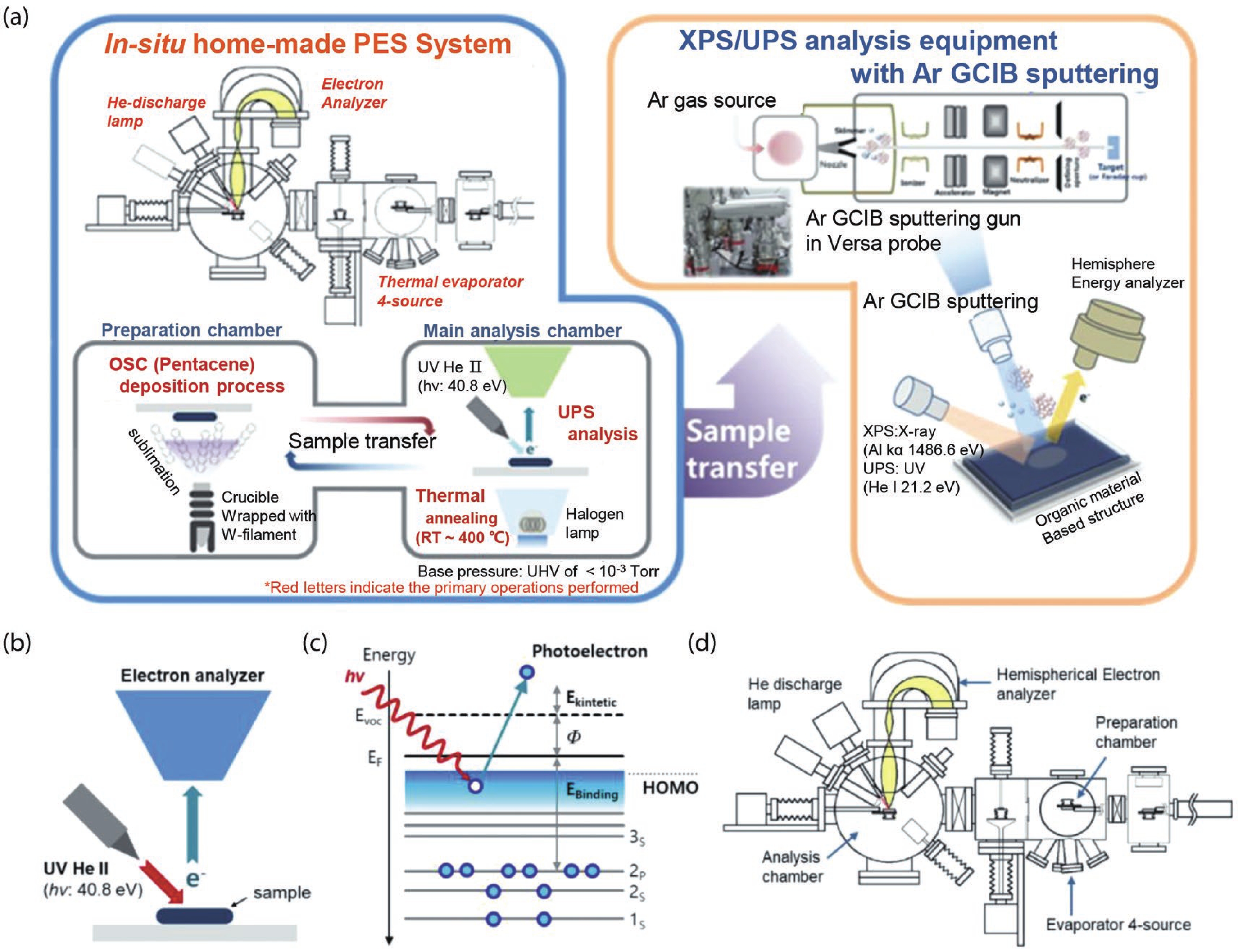
Yun D J, Lee S, Yong K, et al. In situ ultraviolet photoemission spectroscopy measurement of the pentacene-RuO2/Ti contact energy structure. Appl Phys Lett, 2010, 97, 073303 doi: 10.1063/1.3481084
|
| [20] |
Giridharagopal R, Flagg L Q, Harrison J S, et al. Electrochemical strain microscopy probes morphology-induced variations in ion uptake and performance in organic electrochemical transistors. Nat Mater, 2017, 16, 737 doi: 10.1038/nmat4918
|
| [21] |
Hosono N, Terashima A, Kusaka S, et al. Highly responsive nature of porous coordination polymer surfaces imaged by in situ atomic force microscopy. Nat Chem, 2019, 11, 109 doi: 10.1038/s41557-018-0170-0
|
| [22] |
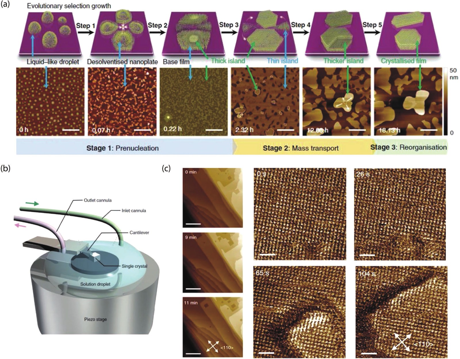
Lee J C, Lee M, Lee H J, et al. Flow patterns: Numerical simulations and in situ optical microscopy connecting flow pattern, crystallization, and thin-film properties for organic transistors with superior device-to-device uniformity. Adv Mater, 2020, 32, 2070357 doi: 10.1002/adma.202070357
|
| [23] |
Wienhold K S, Weindl C L, Yin S S, et al. Following in situ the evolution of morphology and optical properties during printing of thin films for application in non-fullerene acceptor based organic solar cells. ACS Appl Mater Interfaces, 2020, 12, 40381 doi: 10.1021/acsami.0c12390
|
| [24] |
Yang J L, Yan D H. Weak epitaxy growth of organic semiconductor thin films. Chem Soc Rev, 2009, 38, 2634 doi: 10.1039/b815723p
|
| [25] |
Yao Y F, Dong H L, Hu W P. Charge transport in organic and polymeric semiconductors for flexible and stretchable devices. Adv Mater, 2016, 28, 4513 doi: 10.1002/adma.201503007
|
| [26] |
Diao Y, Shaw L, Bao Z N, et al. Morphology control strategies for solution-processed organic semiconductor thin films. Energy Environ Sci, 2014, 7, 2145 doi: 10.1039/C4EE00688G
|
| [27] |
Minari T, Liu C, Kano M, et al. Controlled self-assembly of organic semiconductors for solution-based fabrication of organic field-effect transistors. Adv Mater, 2012, 24, 299 doi: 10.1002/adma.201102554
|
| [28] |
Furchner A, Aulich D. Organic materials for optoelectronic applications. Springer Ser Surf Sci, 2018, 52, 529
|
| [29] |
Li Y, Sun H B, Shi Y, et al. Patterning technology for solution-processed organic crystal field-effect transistors. Sci Technol Adv Mater, 2014, 15, 024203 doi: 10.1088/1468-6996/15/2/024203
|
| [30] |
Gu X D, Shaw L, Gu K, et al. The meniscus-guided deposition of semiconducting polymers. Nat Commun, 2018, 9, 534 doi: 10.1038/s41467-018-02833-9
|
| [31] |
Park K S, Kwok J J, Dilmurat R, et al. Tuning conformation, assembly, and charge transport properties of conjugated polymers by printing flow. Sci Adv, 2019, 5, eaaw7757 doi: 10.1126/sciadv.aaw7757
|
| [32] |
Zhang Z C, Peng B Y, Ji X D, et al. Marangoni-effect-assisted bar-coating method for high-quality organic crystals with compressive and tensile strains. Adv Funct Mater, 2017, 27, 1703443 doi: 10.1002/adfm.201703443
|
| [33] |
Peng B Y, Wang Z R, Chan P K L. A simulation-assisted solution-processing method for a large-area, high-performance C10-DNTT organic semiconductor crystal. J Mater Chem C, 2016, 4, 8628 doi: 10.1039/C6TC03432B
|
| [34] |
Lee J C, Seo H, Lee M, et al. Investigation of the effect of 3D meniscus geometry on fluid dynamics and crystallization via in situ optical microscopy-assisted mathematical modeling. Adv Mater, 2021, 2105035 doi: 10.1002/adma.202105035
|
| [35] |
Chiodini S, Straub A, Donati S, et al. Morphological transitions in organic ultrathin film growth imaged by in situ step-by-step atomic force microscopy. J Phys Chem C, 2020, 124, 14030 doi: 10.1021/acs.jpcc.0c03279
|
| [36] |
Lang S Y, Shi Y, Guo Y G, et al. Insight into the interfacial process and mechanism in lithium-sulfur batteries: An in situ AFM study. Angew Chem Int Ed, 2016, 55, 15835 doi: 10.1002/anie.201608730
|
| [37] |
Kyndiah A, Checa M, Leonardi F, et al. Nanoscale mapping of the conductivity and interfacial capacitance of an electrolyte-gated organic field-effect transistor under operation. Adv Funct Mater, 2021, 31, 2008032 doi: 10.1002/adfm.202008032
|
| [38] |
Chen H L, Li M L, Lu Z Y, et al. Multistep nucleation and growth mechanisms of organic crystals from amorphous solid states. Nat Commun, 2019, 10, 3872 doi: 10.1038/s41467-019-11887-2
|
| [39] |
Rivnay J, Inal S, Salleo A, et al. Organic electrochemical transistors. Nat Rev Mater, 2018, 3, 17086 doi: 10.1038/natrevmats.2017.86
|
| [40] |
Gerasimov J Y, Gabrielsson R, Forchheimer R, et al. An evolvable organic electrochemical transistor for neuromorphic applications. Adv Sci, 2019, 6, 1801339 doi: 10.1002/advs.201801339
|
| [41] |
Spyropoulos G D, Gelinas J N, Khodagholy D. Internal ion-gated organic electrochemical transistor: A building block for integrated bioelectronics. Sci Adv, 2019, 5, eaau7378 doi: 10.1126/sciadv.aau7378
|
| [42] |
Yi Z H, Natale G, Kumar P, et al. Ionic liquid–water mixtures and ion gels as electrolytes for organic electrochemical transistors. J Mater Chem C, 2015, 3, 6549 doi: 10.1039/c5tc00712g
|
| [43] |
Yuan H T, Shimotani H, Ye J T, et al. Electrostatic and electrochemical nature of liquid-gated electric-double-layer transistors based on oxide semiconductors. J Am Chem Soc, 2010, 132, 18402 doi: 10.1021/ja108912x
|
| [44] |
Giovannitti A, Nielsen C B, Sbircea D T, et al. N-type organic electrochemical transistors with stability in water. Nat Commun, 2016, 7, 13066 doi: 10.1038/ncomms13066
|
| [45] |
Lin P, Luo X T, Hsing I M, et al. Organic electrochemical transistors integrated in flexible microfluidic systems and used for label-free DNA sensing. Adv Mater, 2011, 23, 4035 doi: 10.1002/adma.201102017
|
| [46] |
Jimison L H, Tria S A, Khodagholy D, et al. Measurement of barrier tissue integrity with an organic electrochemical transistor. Adv Mater, 2012, 24, 5919 doi: 10.1002/adma.201202612
|
| [47] |
Campana A, Cramer T, Simon D T, et al. Electrocardiographic recording with conformable organic electrochemical transistor fabricated on resorbable bioscaffold. Adv Mater, 2014, 26, 3874 doi: 10.1002/adma.201400263
|
| [48] |
Leleux P, Johnson C, Strakosas X, et al. Ionic liquid gel-assisted electrodes for long-term cutaneous recordings. Adv Healthcare Mater, 2014, 3, 1377 doi: 10.1002/adhm.201300614
|
| [49] |
Gkoupidenis P, Koutsouras D A, Malliaras G G. Neuromorphic device architectures with global connectivity through electrolyte gating. Nat Commun, 2017, 8, 15448 doi: 10.1038/ncomms15448
|
| [50] |
Lin P, Yan F, Yu J J, et al. The application of organic electrochemical transistors in cell-based biosensors. Adv Mater, 2010, 22, 3655 doi: 10.1002/adma.201000971
|
| [51] |
Ji X D, Lau H Y, Ren X C, et al. Bioelectronics: highly sensitive metabolite biosensor based on organic electrochemical transistor integrated with microfluidic channel and poly(N-vinyl-2-pyrrolidone)-capped platinum nanoparticles. Adv Mater Technol, 2016, 1, 1 doi: 10.1002/admt.201670022
|
| [52] |
Sun H D, Gerasimov J, Berggren M, et al. N-Type organic electrochemical transistors: Materials and challenges. J Mater Chem C, 2018, 6, 11778 doi: 10.1039/C8TC03185A
|
| [53] |
Kim S H, Hong K, Xie W, et al. Electrolyte-gated transistors for organic and printed electronics. Adv Mater, 2013, 25, 1822 doi: 10.1002/adma.201202790
|
| [54] |
Strakosas X, Bongo M, Owens R M. The organic electrochemical transistor for biological applications. J Appl Polym Sci, 2015, 132, 1 doi: 10.1002/app.41735
|
| [55] |
Yokota T, Zalar P, Kaltenbrunner M, et al. Ultraflexible organic photonic skin. Sci Adv, 2016, 2, 1 doi: 10.1126/sciadv.1501856
|
| [56] |
Wu Y L, Liu P, Li Y N, et al. Enabling materials for printed electronics. 2006 IEEE LEOS Annual Meeting Conference Proceedings, 2006, 434
|
| [57] |
Ostroverkhova O. Organic optoelectronic materials: Mechanisms and applications. Chem Rev, 2016, 116, 13279 doi: 10.1021/acs.chemrev.6b00127
|
| [58] |
Forrest S R. Electronic appliances on plastic. Nature, 2004, 428, 911 doi: 10.1038/nature02498
|
| [59] |
Rivnay J, Jimison L H, Northrup J E, et al. Large modulation of carrier transport by grain-boundary molecular packing and microstructure in organic thin films. Nat Mater, 2009, 8, 952 doi: 10.1038/nmat2570
|
| [60] |
Yun D J, Chung J, Jung C, et al. Pentacene orientation on source/drain electrodes and its effect on charge carrier transport at pentacene/electrode interface, investigated using in situ ultraviolet photoemission spectroscopy and device characteristics. J Electrochem Soc, 2013, 160, H436 doi: 10.1149/2.038308jes
|
| [61] |
Sanyal M, Schmidt-Hansberg B, Klein M F G, et al. In situ X-ray study of drying-temperature influence on the structural evolution of bulk-heterojunction polymer-fullerene solar cells processed by doctor-blading. Adv Energy Mater, 2011, 1, 363 doi: 10.1002/aenm.201100007
|
| [62] |
Li R P, Khan H U, Payne M M, et al. Heterogeneous nucleation promotes carrier transport in solution-processed organic field-effect transistors. Adv Funct Mater, 2013, 23, 291 doi: 10.1002/adfm.201201264
|
| [63] |
Fang P H, Wu F C, Sheu H S, et al. Analysis of ultrathin organic inverters by using in situ grazing incidence X-ray diffraction under high bending times and low voltage. Org Electron, 2021, 88, 106002 doi: 10.1016/j.orgel.2020.106002
|
| [64] |
Yang D, Löhrer F C, Körstgens V, et al. In-operando study of the effects of solvent additives on the stability of organic solar cells based on PTB7-Th:PC71BM. ACS Energy Lett, 2019, 4, 464 doi: 10.1021/acsenergylett.8b02311
|
| [65] |
Wang G H, Huang K Q, Liu Z, et al. Flexible, low-voltage, and n-type infrared organic phototransistors with enhanced photosensitivity via interface trapping effect. ACS Appl Mater Interfaces, 2018, 10, 36177 doi: 10.1021/acsami.8b12009
|
| [66] |
Song Z Q, Tong Y H, Zhao X L, et al. A flexible conformable artificial organ-damage memory system towards hazardous gas leakage based on a single organic transistor. Mater Horiz, 2019, 6, 717 doi: 10.1039/C8MH01577E
|
| [67] |
Myny K. The development of flexible integrated circuits based on thin-film transistors. Nat Electron, 2018, 1, 30 doi: 10.1038/s41928-017-0008-6
|
| [68] |
Someya T, Kato Y, Sekitani T, et al. Conformable, flexible, large-area networks of pressure and thermal sensors with organic transistor active matrixes. PNAS, 2005, 102, 12321 doi: 10.1073/pnas.0502392102
|
| [69] |
Borchert J W, Peng B Y, Letzkus F, et al. Small contact resistance and high-frequency operation of flexible low-voltage inverted coplanar organic transistors. Nat Commun, 2019, 10, 1119 doi: 10.1038/s41467-019-09119-8
|
| [70] |
Sirringhaus H. Device physics of solution-processed organic field-effect transistors. Adv Mater, 2005, 17, 2411 doi: 10.1002/adma.200501152
|
| [71] |
Giri G, Li R P, Smilgies D M, et al. One-dimensional self-confinement promotes polymorph selection in large-area organic semiconductor thin films. Nat Commun, 2014, 5, 3573 doi: 10.1038/ncomms4573
|
| [72] |
Aliouat M Y, Escoubas S, Benoudia M C, et al. In situ measurements of the structure and strain of a π-conjugated semiconducting polymer under mechanical load. J Appl Phys, 2020, 127, 045108 doi: 10.1063/1.5127226
|
| [73] |
Grodd L S, Mikayelyan E, Dane T, et al. Local scale structural changes of working OFET devices. Nanoscale, 2020, 12, 2434 doi: 10.1039/C9NR07905J
|
| [74] |
Wang C L, Dong H L, Hu W P, et al. Semiconducting π-conjugated systems in field-effect transistors: A material odyssey of organic electronics. Chem Rev, 2012, 112, 2208 doi: 10.1021/cr100380z
|
| [75] |
Bässler H, Köhler A. Charge transport in organic semiconductors. Top Curr Chem, 2012, 312, 1 doi: 10.1007/128_2011_218
|
| [76] |
Olivier Y, Lemaur V, Brédas J L, et al. Charge hopping in organic semiconductors: Influence of molecular parameters on macroscopic mobilities in model one-dimensional stacks. J Phys Chem A, 2006, 110, 6356 doi: 10.1021/jp0571933
|
| [77] |
Yun D J, Chung J, Kim Y, et al. Direct comparative study on the energy level alignments in unoccupied/occupied states of organic semiconductor/electrode interface by constructing in situ photoemission spectroscopy and Ar gas cluster ion beam sputtering integrated analysis system. J Appl Phys, 2014, 116, 153702 doi: 10.1063/1.4897517
|
| [78] |
Braun S, Salaneck W R, Fahlman M. Energy-level alignment at organic/metal and organic/organic interfaces. Adv Mater, 2009, 21, 1450 doi: 10.1002/adma.200802893
|
| [79] |
Koch N, Kahn A, Ghijsen J, et al. Conjugated organic molecules on metal versus polymer electrodes: Demonstration of a key energy level alignment mechanism. Appl Phys Lett, 2002, 82, 70 doi: 10.1063/1.1532102
|
| [80] |
Yun D J, Park S H, Hwang J, et al. In situ photoelectron spectroscopy study on the buffer role of multiwalled carbon nanotubes against thermal degradation in organic conducting composite films with PEDOT:PSS. J Phys Chem C, 2019, 123, 2238 doi: 10.1021/acs.jpcc.8b10345
|
| [81] |
Yun D J, Yun Y, Lee J, et al. In-depth investigation of the correlation between organic semiconductor orientation and energy-level alignment using in situ photoelectron spectroscopy. ACS Appl Mater Interfaces, 2020, 12, 50628 doi: 10.1021/acsami.0c09602
|
| [82] |
Wang C, Ren X C, Xu C H, et al. Organic single crystals: N-type 2D organic single crystals for high-performance organic field-effect transistors and near-infrared phototransistors. Adv Mater, 2018, 30, 1870114 doi: 10.1002/adma.201870114
|
| [83] |
Cai S L, Zhang W G, Zuckermann R N, et al. The organic flatland-recent advances in synthetic 2D organic layers. Adv Mater, 2015, 27, 5762 doi: 10.1002/adma.201500124
|
| [84] |
Yang F X, Cheng S S, Zhang X T, et al. 2D organic materials for optoelectronic applications. Adv Mater, 2018, 30, 1702415 doi: 10.1002/adma.201702415
|


| [1] |
Tsumura A, Koezuka H, Ando T. Macromolecular electronic device: Field-effect transistor with a polythiophene thin film. Appl Phys Lett, 1986, 49, 1210 doi: 10.1063/1.97417
|
| [2] |
Li L Q, Gao P, Wang W C, et al. Growth of ultrathin organic semiconductor microstripes with thickness control in the monolayer precision. Angew Chem Int Ed, 2013, 52, 12530 doi: 10.1002/anie.201306953
|
| [3] |
Yuan Y B, Giri G, Ayzner A L, et al. Ultra-high mobility transparent organic thin film transistors grown by an off-centre spin-coating method. Nat Commun, 2014, 5, 3005 doi: 10.1038/ncomms4005
|
| [4] |
Zhang Y H, Qiao J S, Gao S, et al. Probing carrier transport and structure-property relationship of highly ordered organic semiconductors at the two-dimensional limit. Phys Rev Lett, 2016, 116, 016602 doi: 10.1103/PhysRevLett.116.016602
|
| [5] |
Lin P, Yan F. Organic thin-film transistors for chemical and biological sensing. Adv Mater, 2012, 24, 34 doi: 10.1002/adma.201103334
|
| [6] |
van de Burgt Y, Melianas A, Keene S T, et al. Organic electronics for neuromorphic computing. Nat Electron, 2018, 1, 386 doi: 10.1038/s41928-018-0103-3
|
| [7] |
Minemawari H, Yamada T, Matsui H, et al. Inkjet printing of single-crystal films. Nature, 2011, 475, 364 doi: 10.1038/nature10313
|
| [8] |
Wang C L, Dong H L, Jiang L, et al. Organic semiconductor crystals. Chem Soc Rev, 2018, 47, 422 doi: 10.1039/C7CS00490G
|
| [9] |
Wang Q J, Qian J, Li Y, et al. 2D single-crystalline molecular semiconductors with precise layer definition achieved by floating-coffee-ring-driven assembly. Adv Funct Mater, 2016, 26, 3191 doi: 10.1002/adfm.201600304
|
| [10] |
Qian J, Jiang S, Li S L, et al. Solution-processed 2D molecular crystals: Fabrication techniques, transistor applications, and physics. Adv Mater Technol, 2019, 4, 1800182 doi: 10.1002/admt.201800182
|
| [11] |
Yamamura A, Watanabe S, Uno M, et al. Wafer-scale, layer-controlled organic single crystals for high-speed circuit operation. Sci Adv, 2018, 4, eaao5758 doi: 10.1126/sciadv.aao5758
|
| [12] |
Jiang S, Qian J, Duan Y, et al. Millimeter-sized two-dimensional molecular crystalline semiconductors with precisely defined molecular layers via interfacial-interaction-modulated self-assembly. J Phys Chem Lett, 2018, 9, 6755 doi: 10.1021/acs.jpclett.8b03108
|
| [13] |
Wang Z W, Guo S J, Li H W, et al. The semiconductor/conductor interface piezoresistive effect in an organic transistor for highly sensitive pressure sensors. Adv Mater, 2018, 1805630 doi: 10.1002/adma.201805630
|
| [14] |
Sun W, Gao B, Chi M F, et al. Understanding memristive switching via in situ characterization and device modeling. Nat Commun, 2019, 10, 3453 doi: 10.1038/s41467-019-11411-6
|
| [15] |
Leever B J, Bailey C A, Marks T J, et al. In situ characterization of lifetime and morphology in operating bulk heterojunction organic photovoltaic devices by impedance spectroscopy. Adv Energy Mater, 2012, 2, 120 doi: 10.1002/aenm.201100357
|
| [16] |
Surgailis J, Savva A, Druet V, et al. Mixed conduction in an N-type organic semiconductor in the absence of hydrophilic side-chains. Adv Funct Mater, 2021, 31, 2010165 doi: 10.1002/adfm.202010165
|
| [17] |
Walter S R, Youn J, Emery J D, et al. In-situ probe of gate dielectric-semiconductor interfacial order in organic transistors: Origin and control of large performance sensitivities. J Am Chem Soc, 2012, 134, 11726 doi: 10.1021/ja3036493
|
| [18] |
Chulkin P. In-situ characterisation of charge transport in organic light-emitting diode by impedance spectroscopy. Electron Mater, 2021, 2, 253 doi: 10.3390/electronicmat2020018
|
| [19] |
Yun D J, Lee S, Yong K, et al. In situ ultraviolet photoemission spectroscopy measurement of the pentacene-RuO2/Ti contact energy structure. Appl Phys Lett, 2010, 97, 073303 doi: 10.1063/1.3481084
|
| [20] |
Giridharagopal R, Flagg L Q, Harrison J S, et al. Electrochemical strain microscopy probes morphology-induced variations in ion uptake and performance in organic electrochemical transistors. Nat Mater, 2017, 16, 737 doi: 10.1038/nmat4918
|
| [21] |
Hosono N, Terashima A, Kusaka S, et al. Highly responsive nature of porous coordination polymer surfaces imaged by in situ atomic force microscopy. Nat Chem, 2019, 11, 109 doi: 10.1038/s41557-018-0170-0
|
| [22] |
Lee J C, Lee M, Lee H J, et al. Flow patterns: Numerical simulations and in situ optical microscopy connecting flow pattern, crystallization, and thin-film properties for organic transistors with superior device-to-device uniformity. Adv Mater, 2020, 32, 2070357 doi: 10.1002/adma.202070357
|
| [23] |
Wienhold K S, Weindl C L, Yin S S, et al. Following in situ the evolution of morphology and optical properties during printing of thin films for application in non-fullerene acceptor based organic solar cells. ACS Appl Mater Interfaces, 2020, 12, 40381 doi: 10.1021/acsami.0c12390
|
| [24] |
Yang J L, Yan D H. Weak epitaxy growth of organic semiconductor thin films. Chem Soc Rev, 2009, 38, 2634 doi: 10.1039/b815723p
|
| [25] |
Yao Y F, Dong H L, Hu W P. Charge transport in organic and polymeric semiconductors for flexible and stretchable devices. Adv Mater, 2016, 28, 4513 doi: 10.1002/adma.201503007
|
| [26] |
Diao Y, Shaw L, Bao Z N, et al. Morphology control strategies for solution-processed organic semiconductor thin films. Energy Environ Sci, 2014, 7, 2145 doi: 10.1039/C4EE00688G
|
| [27] |
Minari T, Liu C, Kano M, et al. Controlled self-assembly of organic semiconductors for solution-based fabrication of organic field-effect transistors. Adv Mater, 2012, 24, 299 doi: 10.1002/adma.201102554
|
| [28] |
Furchner A, Aulich D. Organic materials for optoelectronic applications. Springer Ser Surf Sci, 2018, 52, 529
|
| [29] |
Li Y, Sun H B, Shi Y, et al. Patterning technology for solution-processed organic crystal field-effect transistors. Sci Technol Adv Mater, 2014, 15, 024203 doi: 10.1088/1468-6996/15/2/024203
|
| [30] |
Gu X D, Shaw L, Gu K, et al. The meniscus-guided deposition of semiconducting polymers. Nat Commun, 2018, 9, 534 doi: 10.1038/s41467-018-02833-9
|
| [31] |
Park K S, Kwok J J, Dilmurat R, et al. Tuning conformation, assembly, and charge transport properties of conjugated polymers by printing flow. Sci Adv, 2019, 5, eaaw7757 doi: 10.1126/sciadv.aaw7757
|
| [32] |
Zhang Z C, Peng B Y, Ji X D, et al. Marangoni-effect-assisted bar-coating method for high-quality organic crystals with compressive and tensile strains. Adv Funct Mater, 2017, 27, 1703443 doi: 10.1002/adfm.201703443
|
| [33] |
Peng B Y, Wang Z R, Chan P K L. A simulation-assisted solution-processing method for a large-area, high-performance C10-DNTT organic semiconductor crystal. J Mater Chem C, 2016, 4, 8628 doi: 10.1039/C6TC03432B
|
| [34] |
Lee J C, Seo H, Lee M, et al. Investigation of the effect of 3D meniscus geometry on fluid dynamics and crystallization via in situ optical microscopy-assisted mathematical modeling. Adv Mater, 2021, 2105035 doi: 10.1002/adma.202105035
|
| [35] |
Chiodini S, Straub A, Donati S, et al. Morphological transitions in organic ultrathin film growth imaged by in situ step-by-step atomic force microscopy. J Phys Chem C, 2020, 124, 14030 doi: 10.1021/acs.jpcc.0c03279
|
| [36] |
Lang S Y, Shi Y, Guo Y G, et al. Insight into the interfacial process and mechanism in lithium-sulfur batteries: An in situ AFM study. Angew Chem Int Ed, 2016, 55, 15835 doi: 10.1002/anie.201608730
|
| [37] |
Kyndiah A, Checa M, Leonardi F, et al. Nanoscale mapping of the conductivity and interfacial capacitance of an electrolyte-gated organic field-effect transistor under operation. Adv Funct Mater, 2021, 31, 2008032 doi: 10.1002/adfm.202008032
|
| [38] |
Chen H L, Li M L, Lu Z Y, et al. Multistep nucleation and growth mechanisms of organic crystals from amorphous solid states. Nat Commun, 2019, 10, 3872 doi: 10.1038/s41467-019-11887-2
|
| [39] |
Rivnay J, Inal S, Salleo A, et al. Organic electrochemical transistors. Nat Rev Mater, 2018, 3, 17086 doi: 10.1038/natrevmats.2017.86
|
| [40] |
Gerasimov J Y, Gabrielsson R, Forchheimer R, et al. An evolvable organic electrochemical transistor for neuromorphic applications. Adv Sci, 2019, 6, 1801339 doi: 10.1002/advs.201801339
|
| [41] |
Spyropoulos G D, Gelinas J N, Khodagholy D. Internal ion-gated organic electrochemical transistor: A building block for integrated bioelectronics. Sci Adv, 2019, 5, eaau7378 doi: 10.1126/sciadv.aau7378
|
| [42] |
Yi Z H, Natale G, Kumar P, et al. Ionic liquid–water mixtures and ion gels as electrolytes for organic electrochemical transistors. J Mater Chem C, 2015, 3, 6549 doi: 10.1039/c5tc00712g
|
| [43] |
Yuan H T, Shimotani H, Ye J T, et al. Electrostatic and electrochemical nature of liquid-gated electric-double-layer transistors based on oxide semiconductors. J Am Chem Soc, 2010, 132, 18402 doi: 10.1021/ja108912x
|
| [44] |
Giovannitti A, Nielsen C B, Sbircea D T, et al. N-type organic electrochemical transistors with stability in water. Nat Commun, 2016, 7, 13066 doi: 10.1038/ncomms13066
|
| [45] |
Lin P, Luo X T, Hsing I M, et al. Organic electrochemical transistors integrated in flexible microfluidic systems and used for label-free DNA sensing. Adv Mater, 2011, 23, 4035 doi: 10.1002/adma.201102017
|
| [46] |
Jimison L H, Tria S A, Khodagholy D, et al. Measurement of barrier tissue integrity with an organic electrochemical transistor. Adv Mater, 2012, 24, 5919 doi: 10.1002/adma.201202612
|
| [47] |
Campana A, Cramer T, Simon D T, et al. Electrocardiographic recording with conformable organic electrochemical transistor fabricated on resorbable bioscaffold. Adv Mater, 2014, 26, 3874 doi: 10.1002/adma.201400263
|
| [48] |
Leleux P, Johnson C, Strakosas X, et al. Ionic liquid gel-assisted electrodes for long-term cutaneous recordings. Adv Healthcare Mater, 2014, 3, 1377 doi: 10.1002/adhm.201300614
|
| [49] |
Gkoupidenis P, Koutsouras D A, Malliaras G G. Neuromorphic device architectures with global connectivity through electrolyte gating. Nat Commun, 2017, 8, 15448 doi: 10.1038/ncomms15448
|
| [50] |
Lin P, Yan F, Yu J J, et al. The application of organic electrochemical transistors in cell-based biosensors. Adv Mater, 2010, 22, 3655 doi: 10.1002/adma.201000971
|
| [51] |
Ji X D, Lau H Y, Ren X C, et al. Bioelectronics: highly sensitive metabolite biosensor based on organic electrochemical transistor integrated with microfluidic channel and poly(N-vinyl-2-pyrrolidone)-capped platinum nanoparticles. Adv Mater Technol, 2016, 1, 1 doi: 10.1002/admt.201670022
|
| [52] |
Sun H D, Gerasimov J, Berggren M, et al. N-Type organic electrochemical transistors: Materials and challenges. J Mater Chem C, 2018, 6, 11778 doi: 10.1039/C8TC03185A
|
| [53] |
Kim S H, Hong K, Xie W, et al. Electrolyte-gated transistors for organic and printed electronics. Adv Mater, 2013, 25, 1822 doi: 10.1002/adma.201202790
|
| [54] |
Strakosas X, Bongo M, Owens R M. The organic electrochemical transistor for biological applications. J Appl Polym Sci, 2015, 132, 1 doi: 10.1002/app.41735
|
| [55] |
Yokota T, Zalar P, Kaltenbrunner M, et al. Ultraflexible organic photonic skin. Sci Adv, 2016, 2, 1 doi: 10.1126/sciadv.1501856
|
| [56] |
Wu Y L, Liu P, Li Y N, et al. Enabling materials for printed electronics. 2006 IEEE LEOS Annual Meeting Conference Proceedings, 2006, 434
|
| [57] |
Ostroverkhova O. Organic optoelectronic materials: Mechanisms and applications. Chem Rev, 2016, 116, 13279 doi: 10.1021/acs.chemrev.6b00127
|
| [58] |
Forrest S R. Electronic appliances on plastic. Nature, 2004, 428, 911 doi: 10.1038/nature02498
|
| [59] |
Rivnay J, Jimison L H, Northrup J E, et al. Large modulation of carrier transport by grain-boundary molecular packing and microstructure in organic thin films. Nat Mater, 2009, 8, 952 doi: 10.1038/nmat2570
|
| [60] |
Yun D J, Chung J, Jung C, et al. Pentacene orientation on source/drain electrodes and its effect on charge carrier transport at pentacene/electrode interface, investigated using in situ ultraviolet photoemission spectroscopy and device characteristics. J Electrochem Soc, 2013, 160, H436 doi: 10.1149/2.038308jes
|
| [61] |
Sanyal M, Schmidt-Hansberg B, Klein M F G, et al. In situ X-ray study of drying-temperature influence on the structural evolution of bulk-heterojunction polymer-fullerene solar cells processed by doctor-blading. Adv Energy Mater, 2011, 1, 363 doi: 10.1002/aenm.201100007
|
| [62] |
Li R P, Khan H U, Payne M M, et al. Heterogeneous nucleation promotes carrier transport in solution-processed organic field-effect transistors. Adv Funct Mater, 2013, 23, 291 doi: 10.1002/adfm.201201264
|
| [63] |
Fang P H, Wu F C, Sheu H S, et al. Analysis of ultrathin organic inverters by using in situ grazing incidence X-ray diffraction under high bending times and low voltage. Org Electron, 2021, 88, 106002 doi: 10.1016/j.orgel.2020.106002
|
| [64] |
Yang D, Löhrer F C, Körstgens V, et al. In-operando study of the effects of solvent additives on the stability of organic solar cells based on PTB7-Th:PC71BM. ACS Energy Lett, 2019, 4, 464 doi: 10.1021/acsenergylett.8b02311
|
| [65] |
Wang G H, Huang K Q, Liu Z, et al. Flexible, low-voltage, and n-type infrared organic phototransistors with enhanced photosensitivity via interface trapping effect. ACS Appl Mater Interfaces, 2018, 10, 36177 doi: 10.1021/acsami.8b12009
|
| [66] |
Song Z Q, Tong Y H, Zhao X L, et al. A flexible conformable artificial organ-damage memory system towards hazardous gas leakage based on a single organic transistor. Mater Horiz, 2019, 6, 717 doi: 10.1039/C8MH01577E
|
| [67] |
Myny K. The development of flexible integrated circuits based on thin-film transistors. Nat Electron, 2018, 1, 30 doi: 10.1038/s41928-017-0008-6
|
| [68] |
Someya T, Kato Y, Sekitani T, et al. Conformable, flexible, large-area networks of pressure and thermal sensors with organic transistor active matrixes. PNAS, 2005, 102, 12321 doi: 10.1073/pnas.0502392102
|
| [69] |
Borchert J W, Peng B Y, Letzkus F, et al. Small contact resistance and high-frequency operation of flexible low-voltage inverted coplanar organic transistors. Nat Commun, 2019, 10, 1119 doi: 10.1038/s41467-019-09119-8
|
| [70] |
Sirringhaus H. Device physics of solution-processed organic field-effect transistors. Adv Mater, 2005, 17, 2411 doi: 10.1002/adma.200501152
|
| [71] |
Giri G, Li R P, Smilgies D M, et al. One-dimensional self-confinement promotes polymorph selection in large-area organic semiconductor thin films. Nat Commun, 2014, 5, 3573 doi: 10.1038/ncomms4573
|
| [72] |
Aliouat M Y, Escoubas S, Benoudia M C, et al. In situ measurements of the structure and strain of a π-conjugated semiconducting polymer under mechanical load. J Appl Phys, 2020, 127, 045108 doi: 10.1063/1.5127226
|
| [73] |
Grodd L S, Mikayelyan E, Dane T, et al. Local scale structural changes of working OFET devices. Nanoscale, 2020, 12, 2434 doi: 10.1039/C9NR07905J
|
| [74] |
Wang C L, Dong H L, Hu W P, et al. Semiconducting π-conjugated systems in field-effect transistors: A material odyssey of organic electronics. Chem Rev, 2012, 112, 2208 doi: 10.1021/cr100380z
|
| [75] |
Bässler H, Köhler A. Charge transport in organic semiconductors. Top Curr Chem, 2012, 312, 1 doi: 10.1007/128_2011_218
|
| [76] |
Olivier Y, Lemaur V, Brédas J L, et al. Charge hopping in organic semiconductors: Influence of molecular parameters on macroscopic mobilities in model one-dimensional stacks. J Phys Chem A, 2006, 110, 6356 doi: 10.1021/jp0571933
|
| [77] |
Yun D J, Chung J, Kim Y, et al. Direct comparative study on the energy level alignments in unoccupied/occupied states of organic semiconductor/electrode interface by constructing in situ photoemission spectroscopy and Ar gas cluster ion beam sputtering integrated analysis system. J Appl Phys, 2014, 116, 153702 doi: 10.1063/1.4897517
|
| [78] |
Braun S, Salaneck W R, Fahlman M. Energy-level alignment at organic/metal and organic/organic interfaces. Adv Mater, 2009, 21, 1450 doi: 10.1002/adma.200802893
|
| [79] |
Koch N, Kahn A, Ghijsen J, et al. Conjugated organic molecules on metal versus polymer electrodes: Demonstration of a key energy level alignment mechanism. Appl Phys Lett, 2002, 82, 70 doi: 10.1063/1.1532102
|
| [80] |
Yun D J, Park S H, Hwang J, et al. In situ photoelectron spectroscopy study on the buffer role of multiwalled carbon nanotubes against thermal degradation in organic conducting composite films with PEDOT:PSS. J Phys Chem C, 2019, 123, 2238 doi: 10.1021/acs.jpcc.8b10345
|
| [81] |
Yun D J, Yun Y, Lee J, et al. In-depth investigation of the correlation between organic semiconductor orientation and energy-level alignment using in situ photoelectron spectroscopy. ACS Appl Mater Interfaces, 2020, 12, 50628 doi: 10.1021/acsami.0c09602
|
| [82] |
Wang C, Ren X C, Xu C H, et al. Organic single crystals: N-type 2D organic single crystals for high-performance organic field-effect transistors and near-infrared phototransistors. Adv Mater, 2018, 30, 1870114 doi: 10.1002/adma.201870114
|
| [83] |
Cai S L, Zhang W G, Zuckermann R N, et al. The organic flatland-recent advances in synthetic 2D organic layers. Adv Mater, 2015, 27, 5762 doi: 10.1002/adma.201500124
|
| [84] |
Yang F X, Cheng S S, Zhang X T, et al. 2D organic materials for optoelectronic applications. Adv Mater, 2018, 30, 1702415 doi: 10.1002/adma.201702415
|


Article views: 6776 Times PDF downloads: 689 Times Cited by: 0 Times
Received: 02 November 2021 Revised: 10 November 2021 Online: Accepted Manuscript: 06 January 2022Uncorrected proof: 07 January 2022Published: 18 April 2022
| Citation: |
Sai Jiang, Qinyong Dai, Jianhang Guo, Yun Li. In-situ/operando characterization techniques for organic semiconductors and devices[J]. Journal of Semiconductors, 2022, 43(4): 041101. doi: 10.1088/1674-4926/43/4/041101
****
S Jiang, Q Y Dai, J H Guo, Y Li. In-situ/operando characterization techniques for organic semiconductors and devices[J]. J. Semicond, 2022, 43(4): 041101. doi: 10.1088/1674-4926/43/4/041101

|
| [1] |
Tsumura A, Koezuka H, Ando T. Macromolecular electronic device: Field-effect transistor with a polythiophene thin film. Appl Phys Lett, 1986, 49, 1210 doi: 10.1063/1.97417
|
| [2] |
Li L Q, Gao P, Wang W C, et al. Growth of ultrathin organic semiconductor microstripes with thickness control in the monolayer precision. Angew Chem Int Ed, 2013, 52, 12530 doi: 10.1002/anie.201306953
|
| [3] |
Yuan Y B, Giri G, Ayzner A L, et al. Ultra-high mobility transparent organic thin film transistors grown by an off-centre spin-coating method. Nat Commun, 2014, 5, 3005 doi: 10.1038/ncomms4005
|
| [4] |
Zhang Y H, Qiao J S, Gao S, et al. Probing carrier transport and structure-property relationship of highly ordered organic semiconductors at the two-dimensional limit. Phys Rev Lett, 2016, 116, 016602 doi: 10.1103/PhysRevLett.116.016602
|
| [5] |
Lin P, Yan F. Organic thin-film transistors for chemical and biological sensing. Adv Mater, 2012, 24, 34 doi: 10.1002/adma.201103334
|
| [6] |
van de Burgt Y, Melianas A, Keene S T, et al. Organic electronics for neuromorphic computing. Nat Electron, 2018, 1, 386 doi: 10.1038/s41928-018-0103-3
|
| [7] |
Minemawari H, Yamada T, Matsui H, et al. Inkjet printing of single-crystal films. Nature, 2011, 475, 364 doi: 10.1038/nature10313
|
| [8] |
Wang C L, Dong H L, Jiang L, et al. Organic semiconductor crystals. Chem Soc Rev, 2018, 47, 422 doi: 10.1039/C7CS00490G
|
| [9] |
Wang Q J, Qian J, Li Y, et al. 2D single-crystalline molecular semiconductors with precise layer definition achieved by floating-coffee-ring-driven assembly. Adv Funct Mater, 2016, 26, 3191 doi: 10.1002/adfm.201600304
|
| [10] |
Qian J, Jiang S, Li S L, et al. Solution-processed 2D molecular crystals: Fabrication techniques, transistor applications, and physics. Adv Mater Technol, 2019, 4, 1800182 doi: 10.1002/admt.201800182
|
| [11] |
Yamamura A, Watanabe S, Uno M, et al. Wafer-scale, layer-controlled organic single crystals for high-speed circuit operation. Sci Adv, 2018, 4, eaao5758 doi: 10.1126/sciadv.aao5758
|
| [12] |
Jiang S, Qian J, Duan Y, et al. Millimeter-sized two-dimensional molecular crystalline semiconductors with precisely defined molecular layers via interfacial-interaction-modulated self-assembly. J Phys Chem Lett, 2018, 9, 6755 doi: 10.1021/acs.jpclett.8b03108
|
| [13] |
Wang Z W, Guo S J, Li H W, et al. The semiconductor/conductor interface piezoresistive effect in an organic transistor for highly sensitive pressure sensors. Adv Mater, 2018, 1805630 doi: 10.1002/adma.201805630
|
| [14] |
Sun W, Gao B, Chi M F, et al. Understanding memristive switching via in situ characterization and device modeling. Nat Commun, 2019, 10, 3453 doi: 10.1038/s41467-019-11411-6
|
| [15] |
Leever B J, Bailey C A, Marks T J, et al. In situ characterization of lifetime and morphology in operating bulk heterojunction organic photovoltaic devices by impedance spectroscopy. Adv Energy Mater, 2012, 2, 120 doi: 10.1002/aenm.201100357
|
| [16] |
Surgailis J, Savva A, Druet V, et al. Mixed conduction in an N-type organic semiconductor in the absence of hydrophilic side-chains. Adv Funct Mater, 2021, 31, 2010165 doi: 10.1002/adfm.202010165
|
| [17] |
Walter S R, Youn J, Emery J D, et al. In-situ probe of gate dielectric-semiconductor interfacial order in organic transistors: Origin and control of large performance sensitivities. J Am Chem Soc, 2012, 134, 11726 doi: 10.1021/ja3036493
|
| [18] |
Chulkin P. In-situ characterisation of charge transport in organic light-emitting diode by impedance spectroscopy. Electron Mater, 2021, 2, 253 doi: 10.3390/electronicmat2020018
|
| [19] |
Yun D J, Lee S, Yong K, et al. In situ ultraviolet photoemission spectroscopy measurement of the pentacene-RuO2/Ti contact energy structure. Appl Phys Lett, 2010, 97, 073303 doi: 10.1063/1.3481084
|
| [20] |
Giridharagopal R, Flagg L Q, Harrison J S, et al. Electrochemical strain microscopy probes morphology-induced variations in ion uptake and performance in organic electrochemical transistors. Nat Mater, 2017, 16, 737 doi: 10.1038/nmat4918
|
| [21] |
Hosono N, Terashima A, Kusaka S, et al. Highly responsive nature of porous coordination polymer surfaces imaged by in situ atomic force microscopy. Nat Chem, 2019, 11, 109 doi: 10.1038/s41557-018-0170-0
|
| [22] |
Lee J C, Lee M, Lee H J, et al. Flow patterns: Numerical simulations and in situ optical microscopy connecting flow pattern, crystallization, and thin-film properties for organic transistors with superior device-to-device uniformity. Adv Mater, 2020, 32, 2070357 doi: 10.1002/adma.202070357
|
| [23] |
Wienhold K S, Weindl C L, Yin S S, et al. Following in situ the evolution of morphology and optical properties during printing of thin films for application in non-fullerene acceptor based organic solar cells. ACS Appl Mater Interfaces, 2020, 12, 40381 doi: 10.1021/acsami.0c12390
|
| [24] |
Yang J L, Yan D H. Weak epitaxy growth of organic semiconductor thin films. Chem Soc Rev, 2009, 38, 2634 doi: 10.1039/b815723p
|
| [25] |
Yao Y F, Dong H L, Hu W P. Charge transport in organic and polymeric semiconductors for flexible and stretchable devices. Adv Mater, 2016, 28, 4513 doi: 10.1002/adma.201503007
|
| [26] |
Diao Y, Shaw L, Bao Z N, et al. Morphology control strategies for solution-processed organic semiconductor thin films. Energy Environ Sci, 2014, 7, 2145 doi: 10.1039/C4EE00688G
|
| [27] |
Minari T, Liu C, Kano M, et al. Controlled self-assembly of organic semiconductors for solution-based fabrication of organic field-effect transistors. Adv Mater, 2012, 24, 299 doi: 10.1002/adma.201102554
|
| [28] |
Furchner A, Aulich D. Organic materials for optoelectronic applications. Springer Ser Surf Sci, 2018, 52, 529
|
| [29] |
Li Y, Sun H B, Shi Y, et al. Patterning technology for solution-processed organic crystal field-effect transistors. Sci Technol Adv Mater, 2014, 15, 024203 doi: 10.1088/1468-6996/15/2/024203
|
| [30] |
Gu X D, Shaw L, Gu K, et al. The meniscus-guided deposition of semiconducting polymers. Nat Commun, 2018, 9, 534 doi: 10.1038/s41467-018-02833-9
|
| [31] |
Park K S, Kwok J J, Dilmurat R, et al. Tuning conformation, assembly, and charge transport properties of conjugated polymers by printing flow. Sci Adv, 2019, 5, eaaw7757 doi: 10.1126/sciadv.aaw7757
|
| [32] |
Zhang Z C, Peng B Y, Ji X D, et al. Marangoni-effect-assisted bar-coating method for high-quality organic crystals with compressive and tensile strains. Adv Funct Mater, 2017, 27, 1703443 doi: 10.1002/adfm.201703443
|
| [33] |
Peng B Y, Wang Z R, Chan P K L. A simulation-assisted solution-processing method for a large-area, high-performance C10-DNTT organic semiconductor crystal. J Mater Chem C, 2016, 4, 8628 doi: 10.1039/C6TC03432B
|
| [34] |
Lee J C, Seo H, Lee M, et al. Investigation of the effect of 3D meniscus geometry on fluid dynamics and crystallization via in situ optical microscopy-assisted mathematical modeling. Adv Mater, 2021, 2105035 doi: 10.1002/adma.202105035
|
| [35] |
Chiodini S, Straub A, Donati S, et al. Morphological transitions in organic ultrathin film growth imaged by in situ step-by-step atomic force microscopy. J Phys Chem C, 2020, 124, 14030 doi: 10.1021/acs.jpcc.0c03279
|
| [36] |
Lang S Y, Shi Y, Guo Y G, et al. Insight into the interfacial process and mechanism in lithium-sulfur batteries: An in situ AFM study. Angew Chem Int Ed, 2016, 55, 15835 doi: 10.1002/anie.201608730
|
| [37] |
Kyndiah A, Checa M, Leonardi F, et al. Nanoscale mapping of the conductivity and interfacial capacitance of an electrolyte-gated organic field-effect transistor under operation. Adv Funct Mater, 2021, 31, 2008032 doi: 10.1002/adfm.202008032
|
| [38] |
Chen H L, Li M L, Lu Z Y, et al. Multistep nucleation and growth mechanisms of organic crystals from amorphous solid states. Nat Commun, 2019, 10, 3872 doi: 10.1038/s41467-019-11887-2
|
| [39] |
Rivnay J, Inal S, Salleo A, et al. Organic electrochemical transistors. Nat Rev Mater, 2018, 3, 17086 doi: 10.1038/natrevmats.2017.86
|
| [40] |
Gerasimov J Y, Gabrielsson R, Forchheimer R, et al. An evolvable organic electrochemical transistor for neuromorphic applications. Adv Sci, 2019, 6, 1801339 doi: 10.1002/advs.201801339
|
| [41] |
Spyropoulos G D, Gelinas J N, Khodagholy D. Internal ion-gated organic electrochemical transistor: A building block for integrated bioelectronics. Sci Adv, 2019, 5, eaau7378 doi: 10.1126/sciadv.aau7378
|
| [42] |
Yi Z H, Natale G, Kumar P, et al. Ionic liquid–water mixtures and ion gels as electrolytes for organic electrochemical transistors. J Mater Chem C, 2015, 3, 6549 doi: 10.1039/c5tc00712g
|
| [43] |
Yuan H T, Shimotani H, Ye J T, et al. Electrostatic and electrochemical nature of liquid-gated electric-double-layer transistors based on oxide semiconductors. J Am Chem Soc, 2010, 132, 18402 doi: 10.1021/ja108912x
|
| [44] |
Giovannitti A, Nielsen C B, Sbircea D T, et al. N-type organic electrochemical transistors with stability in water. Nat Commun, 2016, 7, 13066 doi: 10.1038/ncomms13066
|
| [45] |
Lin P, Luo X T, Hsing I M, et al. Organic electrochemical transistors integrated in flexible microfluidic systems and used for label-free DNA sensing. Adv Mater, 2011, 23, 4035 doi: 10.1002/adma.201102017
|
| [46] |
Jimison L H, Tria S A, Khodagholy D, et al. Measurement of barrier tissue integrity with an organic electrochemical transistor. Adv Mater, 2012, 24, 5919 doi: 10.1002/adma.201202612
|
| [47] |
Campana A, Cramer T, Simon D T, et al. Electrocardiographic recording with conformable organic electrochemical transistor fabricated on resorbable bioscaffold. Adv Mater, 2014, 26, 3874 doi: 10.1002/adma.201400263
|
| [48] |
Leleux P, Johnson C, Strakosas X, et al. Ionic liquid gel-assisted electrodes for long-term cutaneous recordings. Adv Healthcare Mater, 2014, 3, 1377 doi: 10.1002/adhm.201300614
|
| [49] |
Gkoupidenis P, Koutsouras D A, Malliaras G G. Neuromorphic device architectures with global connectivity through electrolyte gating. Nat Commun, 2017, 8, 15448 doi: 10.1038/ncomms15448
|
| [50] |
Lin P, Yan F, Yu J J, et al. The application of organic electrochemical transistors in cell-based biosensors. Adv Mater, 2010, 22, 3655 doi: 10.1002/adma.201000971
|
| [51] |
Ji X D, Lau H Y, Ren X C, et al. Bioelectronics: highly sensitive metabolite biosensor based on organic electrochemical transistor integrated with microfluidic channel and poly(N-vinyl-2-pyrrolidone)-capped platinum nanoparticles. Adv Mater Technol, 2016, 1, 1 doi: 10.1002/admt.201670022
|
| [52] |
Sun H D, Gerasimov J, Berggren M, et al. N-Type organic electrochemical transistors: Materials and challenges. J Mater Chem C, 2018, 6, 11778 doi: 10.1039/C8TC03185A
|
| [53] |
Kim S H, Hong K, Xie W, et al. Electrolyte-gated transistors for organic and printed electronics. Adv Mater, 2013, 25, 1822 doi: 10.1002/adma.201202790
|
| [54] |
Strakosas X, Bongo M, Owens R M. The organic electrochemical transistor for biological applications. J Appl Polym Sci, 2015, 132, 1 doi: 10.1002/app.41735
|
| [55] |
Yokota T, Zalar P, Kaltenbrunner M, et al. Ultraflexible organic photonic skin. Sci Adv, 2016, 2, 1 doi: 10.1126/sciadv.1501856
|
| [56] |
Wu Y L, Liu P, Li Y N, et al. Enabling materials for printed electronics. 2006 IEEE LEOS Annual Meeting Conference Proceedings, 2006, 434
|
| [57] |
Ostroverkhova O. Organic optoelectronic materials: Mechanisms and applications. Chem Rev, 2016, 116, 13279 doi: 10.1021/acs.chemrev.6b00127
|
| [58] |
Forrest S R. Electronic appliances on plastic. Nature, 2004, 428, 911 doi: 10.1038/nature02498
|
| [59] |
Rivnay J, Jimison L H, Northrup J E, et al. Large modulation of carrier transport by grain-boundary molecular packing and microstructure in organic thin films. Nat Mater, 2009, 8, 952 doi: 10.1038/nmat2570
|
| [60] |
Yun D J, Chung J, Jung C, et al. Pentacene orientation on source/drain electrodes and its effect on charge carrier transport at pentacene/electrode interface, investigated using in situ ultraviolet photoemission spectroscopy and device characteristics. J Electrochem Soc, 2013, 160, H436 doi: 10.1149/2.038308jes
|
| [61] |
Sanyal M, Schmidt-Hansberg B, Klein M F G, et al. In situ X-ray study of drying-temperature influence on the structural evolution of bulk-heterojunction polymer-fullerene solar cells processed by doctor-blading. Adv Energy Mater, 2011, 1, 363 doi: 10.1002/aenm.201100007
|
| [62] |
Li R P, Khan H U, Payne M M, et al. Heterogeneous nucleation promotes carrier transport in solution-processed organic field-effect transistors. Adv Funct Mater, 2013, 23, 291 doi: 10.1002/adfm.201201264
|
| [63] |
Fang P H, Wu F C, Sheu H S, et al. Analysis of ultrathin organic inverters by using in situ grazing incidence X-ray diffraction under high bending times and low voltage. Org Electron, 2021, 88, 106002 doi: 10.1016/j.orgel.2020.106002
|
| [64] |
Yang D, Löhrer F C, Körstgens V, et al. In-operando study of the effects of solvent additives on the stability of organic solar cells based on PTB7-Th:PC71BM. ACS Energy Lett, 2019, 4, 464 doi: 10.1021/acsenergylett.8b02311
|
| [65] |
Wang G H, Huang K Q, Liu Z, et al. Flexible, low-voltage, and n-type infrared organic phototransistors with enhanced photosensitivity via interface trapping effect. ACS Appl Mater Interfaces, 2018, 10, 36177 doi: 10.1021/acsami.8b12009
|
| [66] |
Song Z Q, Tong Y H, Zhao X L, et al. A flexible conformable artificial organ-damage memory system towards hazardous gas leakage based on a single organic transistor. Mater Horiz, 2019, 6, 717 doi: 10.1039/C8MH01577E
|
| [67] |
Myny K. The development of flexible integrated circuits based on thin-film transistors. Nat Electron, 2018, 1, 30 doi: 10.1038/s41928-017-0008-6
|
| [68] |
Someya T, Kato Y, Sekitani T, et al. Conformable, flexible, large-area networks of pressure and thermal sensors with organic transistor active matrixes. PNAS, 2005, 102, 12321 doi: 10.1073/pnas.0502392102
|
| [69] |
Borchert J W, Peng B Y, Letzkus F, et al. Small contact resistance and high-frequency operation of flexible low-voltage inverted coplanar organic transistors. Nat Commun, 2019, 10, 1119 doi: 10.1038/s41467-019-09119-8
|
| [70] |
Sirringhaus H. Device physics of solution-processed organic field-effect transistors. Adv Mater, 2005, 17, 2411 doi: 10.1002/adma.200501152
|
| [71] |
Giri G, Li R P, Smilgies D M, et al. One-dimensional self-confinement promotes polymorph selection in large-area organic semiconductor thin films. Nat Commun, 2014, 5, 3573 doi: 10.1038/ncomms4573
|
| [72] |
Aliouat M Y, Escoubas S, Benoudia M C, et al. In situ measurements of the structure and strain of a π-conjugated semiconducting polymer under mechanical load. J Appl Phys, 2020, 127, 045108 doi: 10.1063/1.5127226
|
| [73] |
Grodd L S, Mikayelyan E, Dane T, et al. Local scale structural changes of working OFET devices. Nanoscale, 2020, 12, 2434 doi: 10.1039/C9NR07905J
|
| [74] |
Wang C L, Dong H L, Hu W P, et al. Semiconducting π-conjugated systems in field-effect transistors: A material odyssey of organic electronics. Chem Rev, 2012, 112, 2208 doi: 10.1021/cr100380z
|
| [75] |
Bässler H, Köhler A. Charge transport in organic semiconductors. Top Curr Chem, 2012, 312, 1 doi: 10.1007/128_2011_218
|
| [76] |
Olivier Y, Lemaur V, Brédas J L, et al. Charge hopping in organic semiconductors: Influence of molecular parameters on macroscopic mobilities in model one-dimensional stacks. J Phys Chem A, 2006, 110, 6356 doi: 10.1021/jp0571933
|
| [77] |
Yun D J, Chung J, Kim Y, et al. Direct comparative study on the energy level alignments in unoccupied/occupied states of organic semiconductor/electrode interface by constructing in situ photoemission spectroscopy and Ar gas cluster ion beam sputtering integrated analysis system. J Appl Phys, 2014, 116, 153702 doi: 10.1063/1.4897517
|
| [78] |
Braun S, Salaneck W R, Fahlman M. Energy-level alignment at organic/metal and organic/organic interfaces. Adv Mater, 2009, 21, 1450 doi: 10.1002/adma.200802893
|
| [79] |
Koch N, Kahn A, Ghijsen J, et al. Conjugated organic molecules on metal versus polymer electrodes: Demonstration of a key energy level alignment mechanism. Appl Phys Lett, 2002, 82, 70 doi: 10.1063/1.1532102
|
| [80] |
Yun D J, Park S H, Hwang J, et al. In situ photoelectron spectroscopy study on the buffer role of multiwalled carbon nanotubes against thermal degradation in organic conducting composite films with PEDOT:PSS. J Phys Chem C, 2019, 123, 2238 doi: 10.1021/acs.jpcc.8b10345
|
| [81] |
Yun D J, Yun Y, Lee J, et al. In-depth investigation of the correlation between organic semiconductor orientation and energy-level alignment using in situ photoelectron spectroscopy. ACS Appl Mater Interfaces, 2020, 12, 50628 doi: 10.1021/acsami.0c09602
|
| [82] |
Wang C, Ren X C, Xu C H, et al. Organic single crystals: N-type 2D organic single crystals for high-performance organic field-effect transistors and near-infrared phototransistors. Adv Mater, 2018, 30, 1870114 doi: 10.1002/adma.201870114
|
| [83] |
Cai S L, Zhang W G, Zuckermann R N, et al. The organic flatland-recent advances in synthetic 2D organic layers. Adv Mater, 2015, 27, 5762 doi: 10.1002/adma.201500124
|
| [84] |
Yang F X, Cheng S S, Zhang X T, et al. 2D organic materials for optoelectronic applications. Adv Mater, 2018, 30, 1702415 doi: 10.1002/adma.201702415
|

 WeChat ID
Journal of Semiconductors © 2017 All Rights Reserved 京ICP备05085259号-2

 DownLoad:

