Issue Browser
Volume 43, Issue 10,
Oct 2022

J. Semicond.
2022, 43(10): 101301 doi: 10.1088/1674-4926/43/10/101301
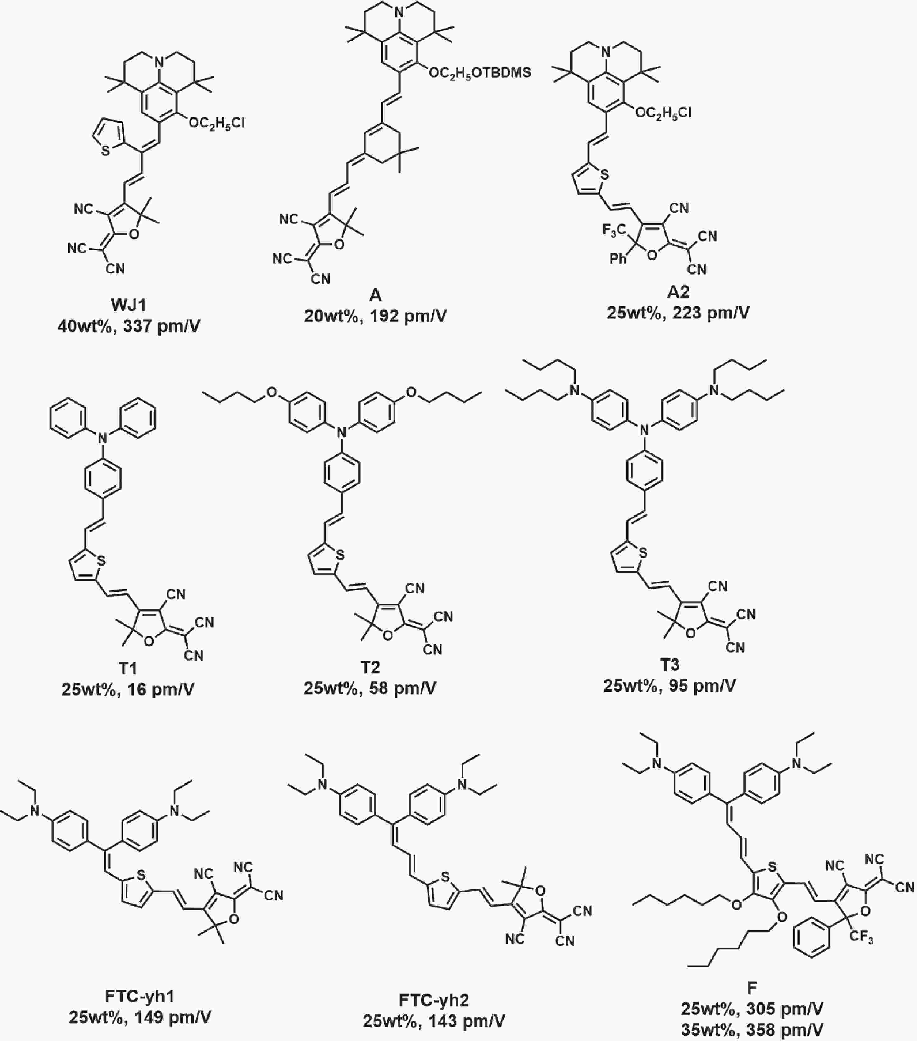
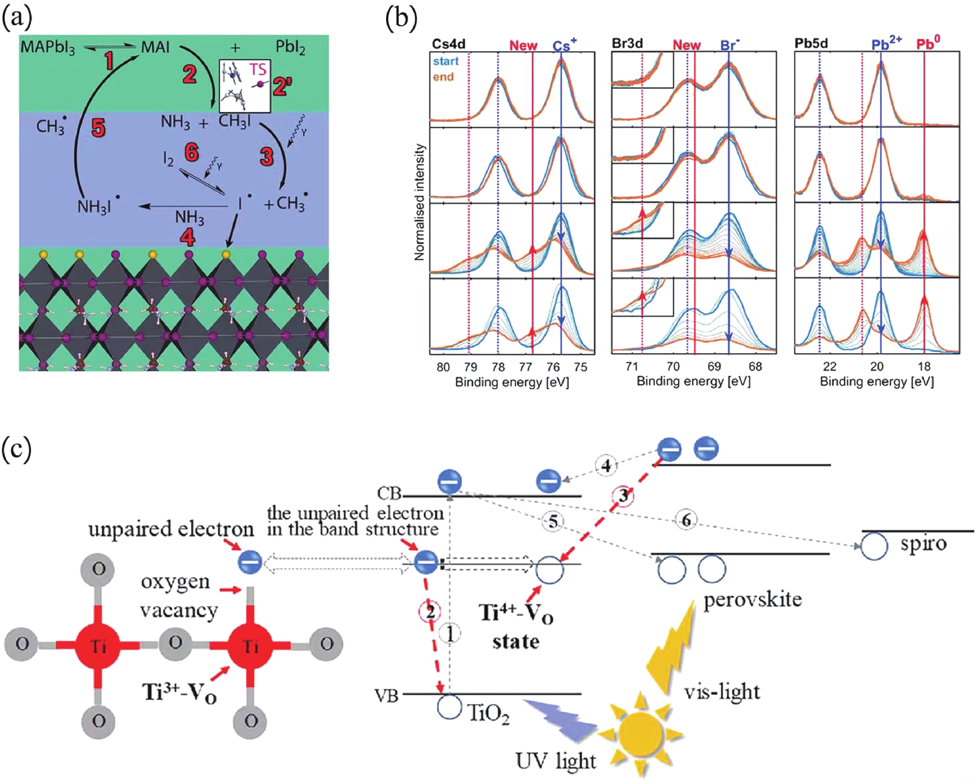
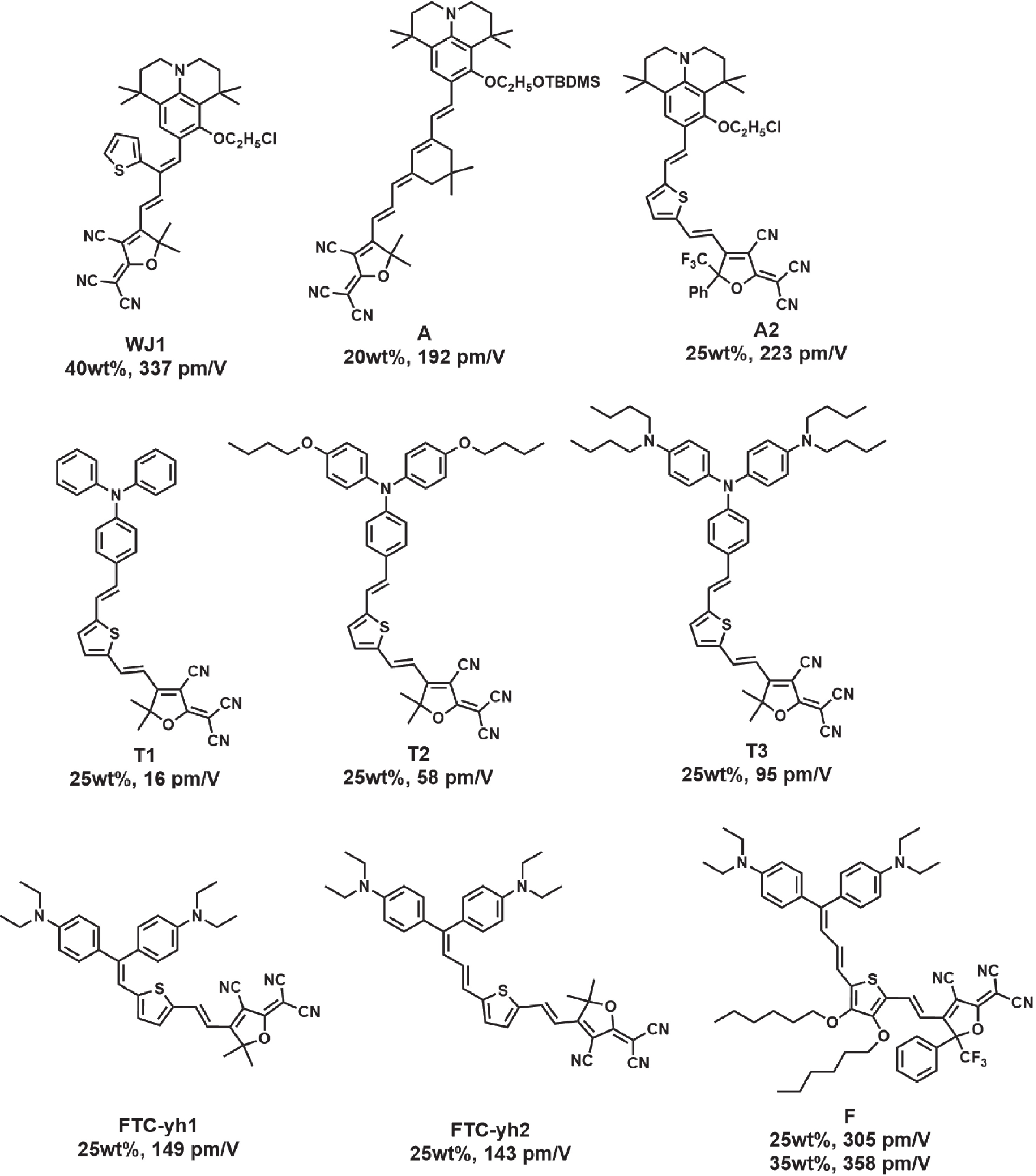
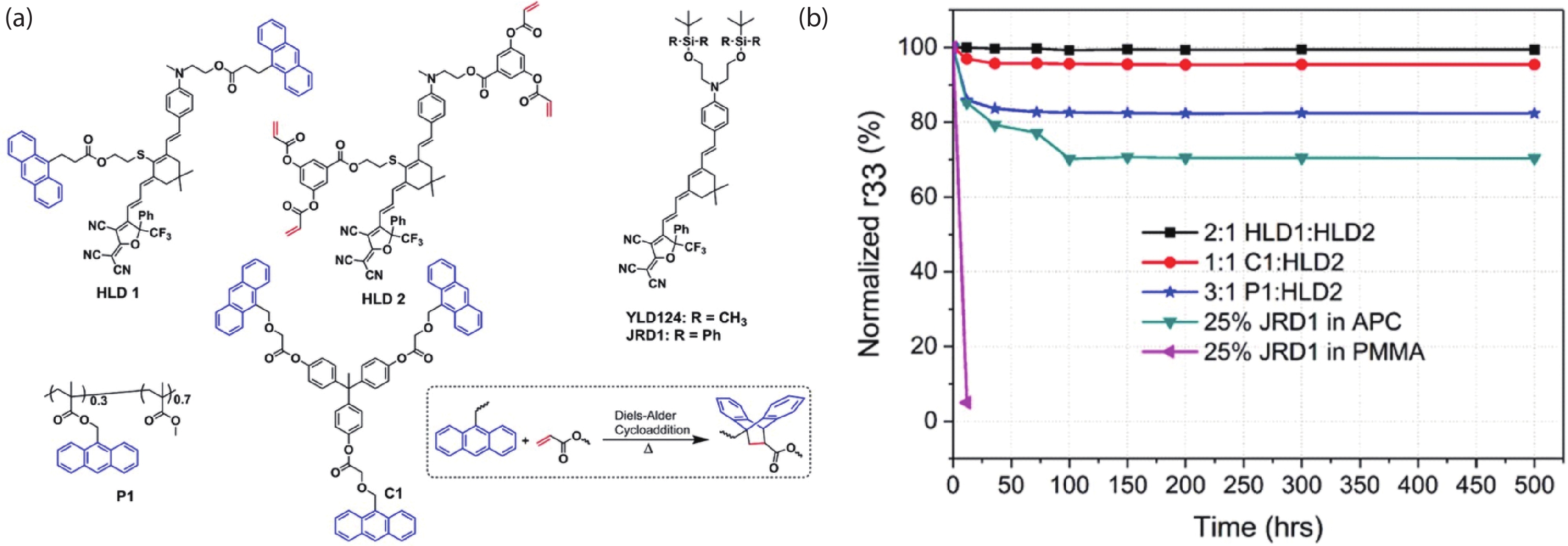
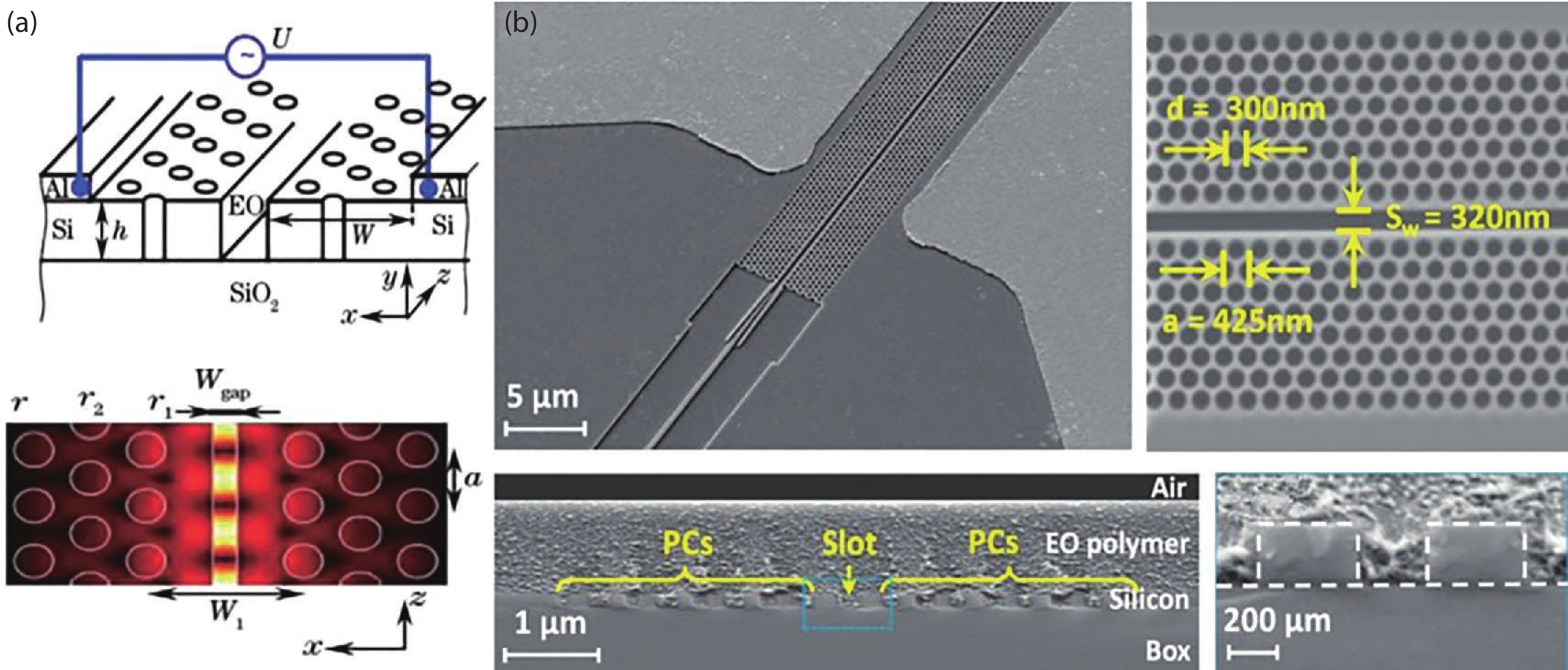
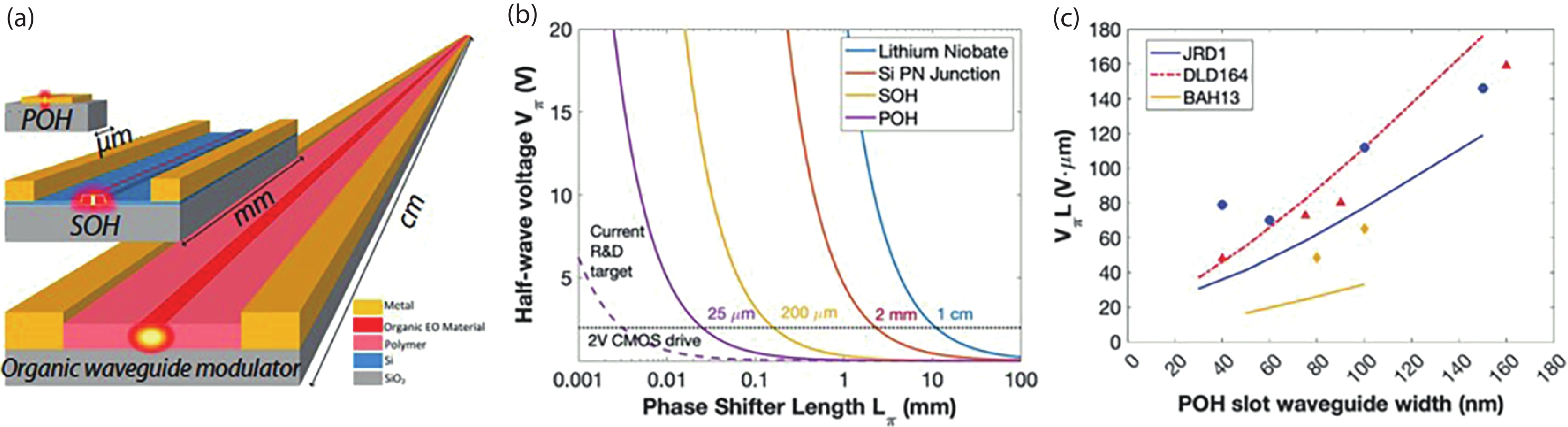
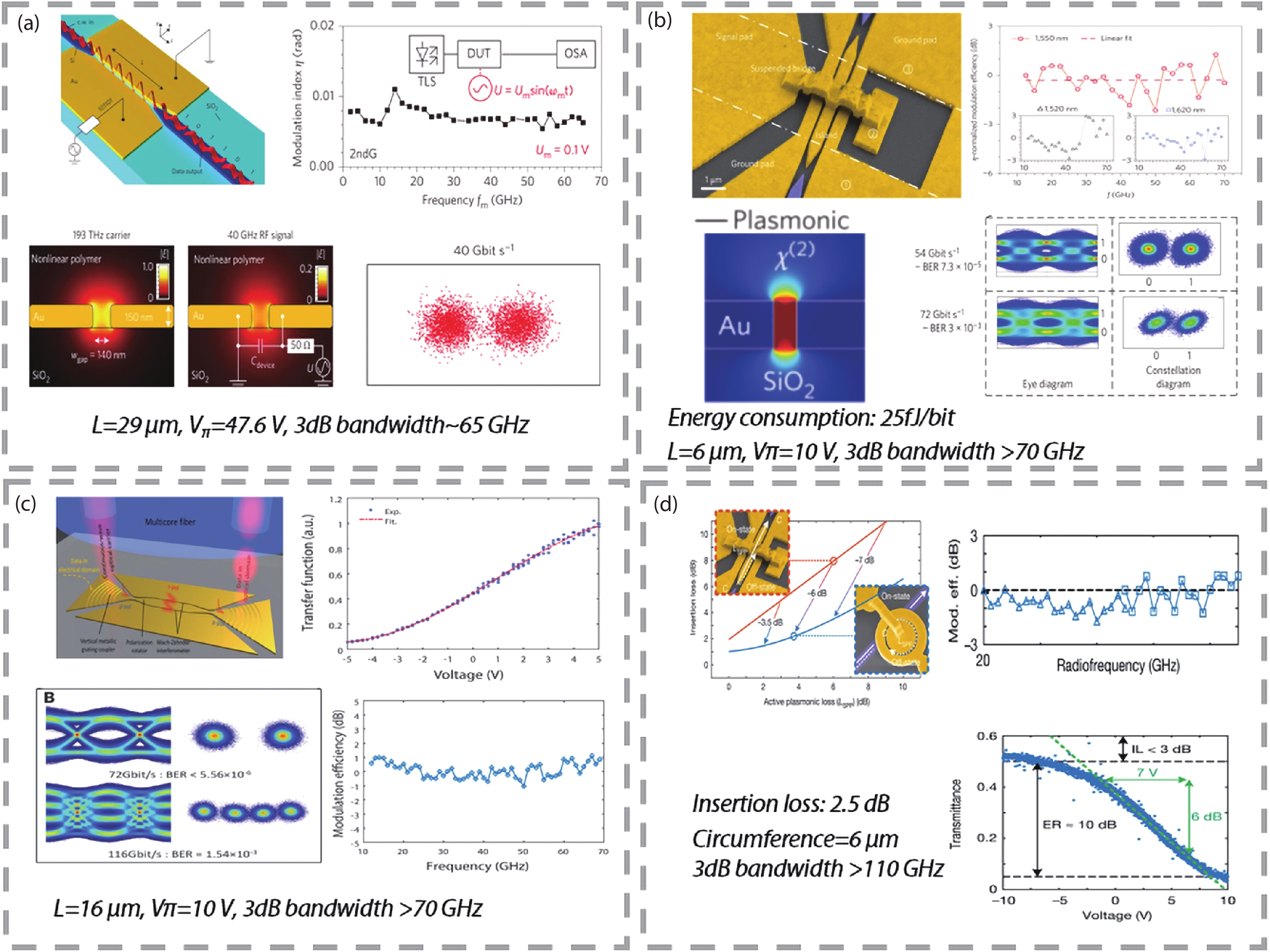
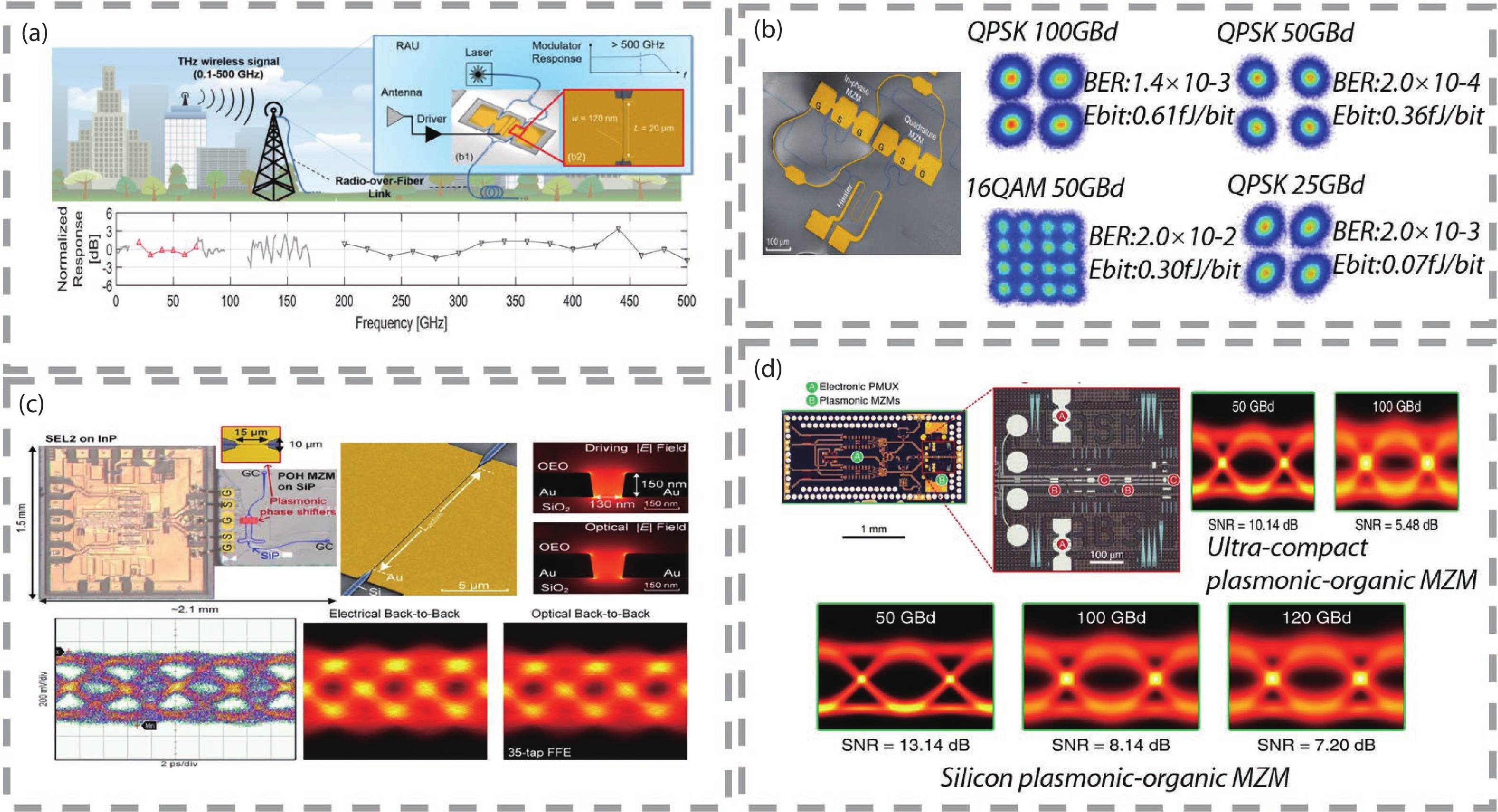
High performance electro-optic modulator, as the key device of integrated ultra-wideband optical systems, have become the focus of research. Meanwhile, the organic-based hybrid electro-optic modulators, which make full use of the advantages of organic electro-optic (OEO) materials (e.g. high electro-optic coefficient, fast response speed, high bandwidth, easy processing/integration and low cost) have attracted considerable attention. In this paper, we introduce a series of high-performance OEO materials that exhibit good properties in electro-optic activity and thermal stability. In addition, the recent progress of organic-based hybrid electro-optic devices is reviewed, including photonic crystal-organic hybrid (PCOH), silicon-organic hybrid (SOH) and plasmonic-organic hybrid (POH) modulators. A high-performance integrated optical platform based on OEO materials is a promising solution for growing high speeds and low power consumption in compact sizes.


J. Semicond.
2022, 43(10): 103101 doi: 10.1088/1674-4926/43/10/103101
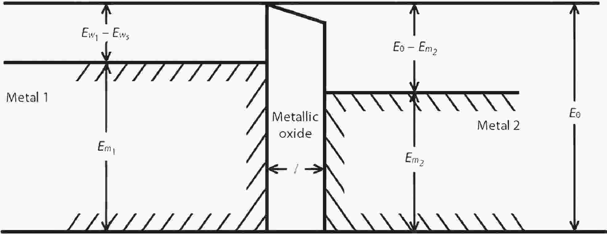
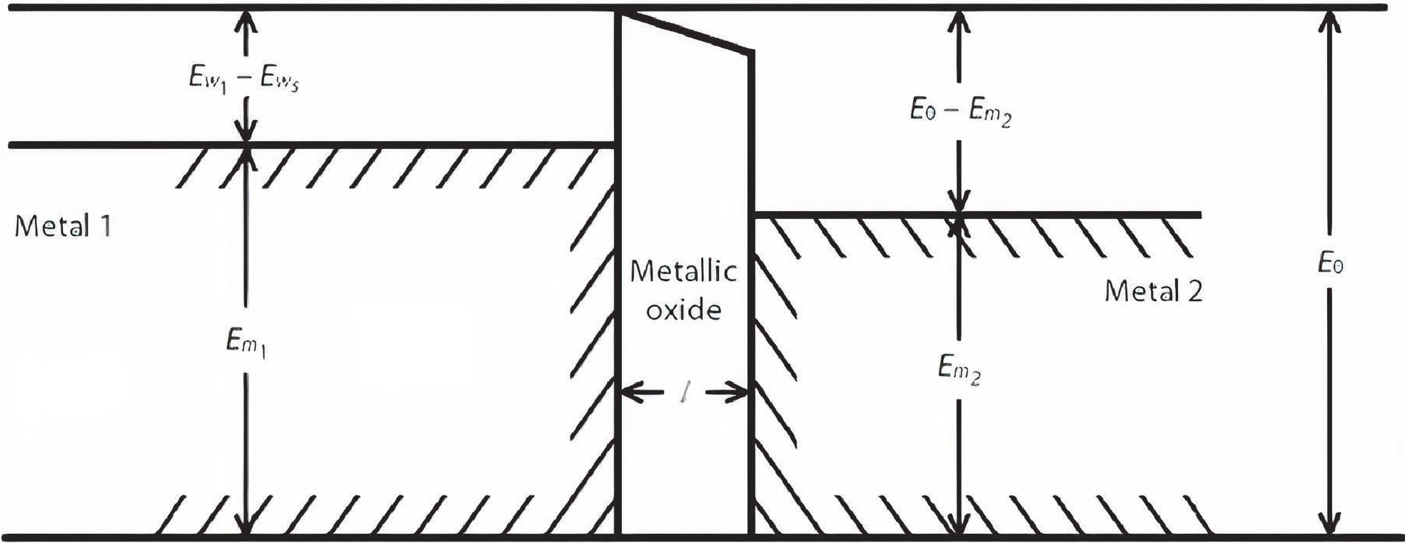
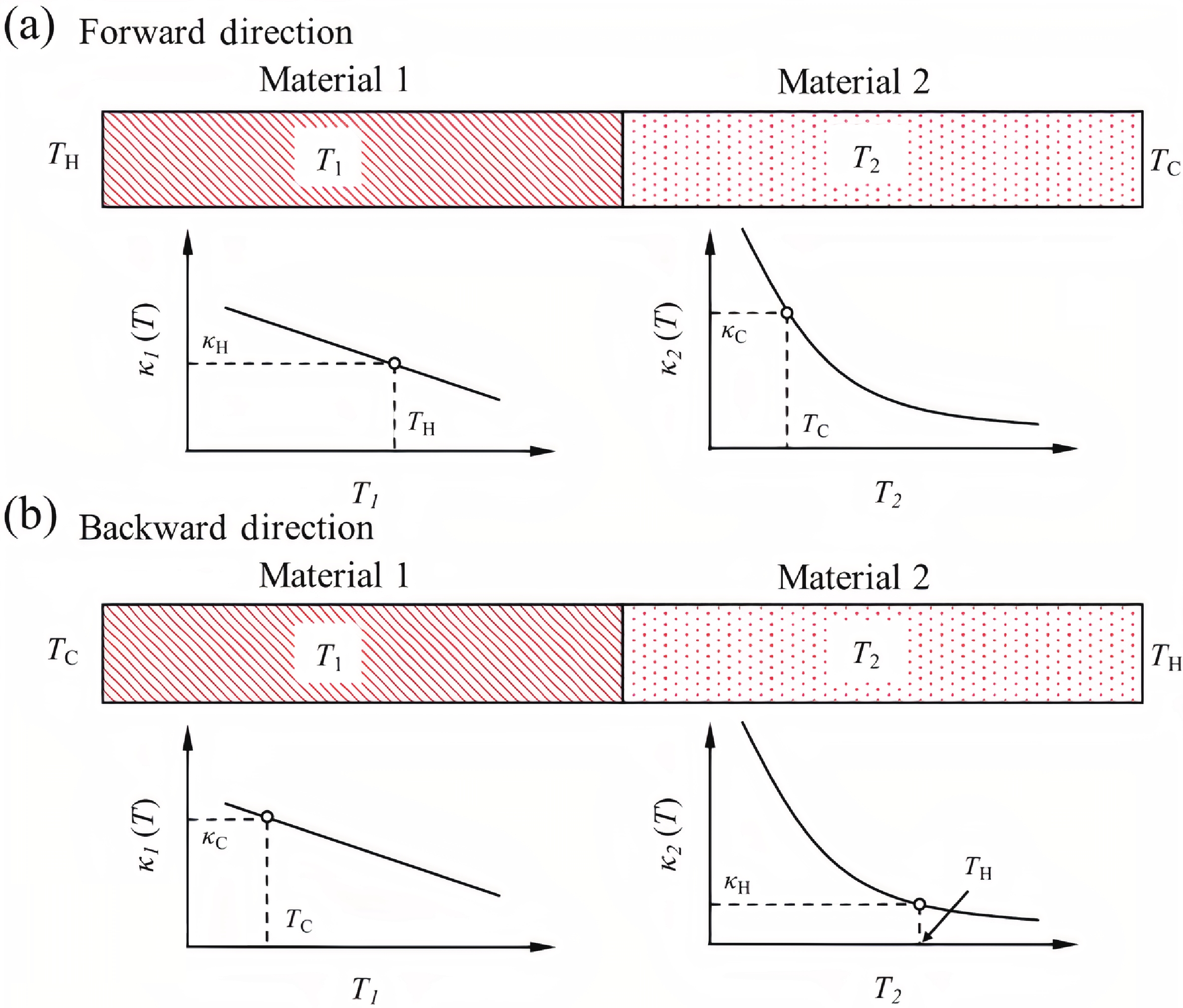
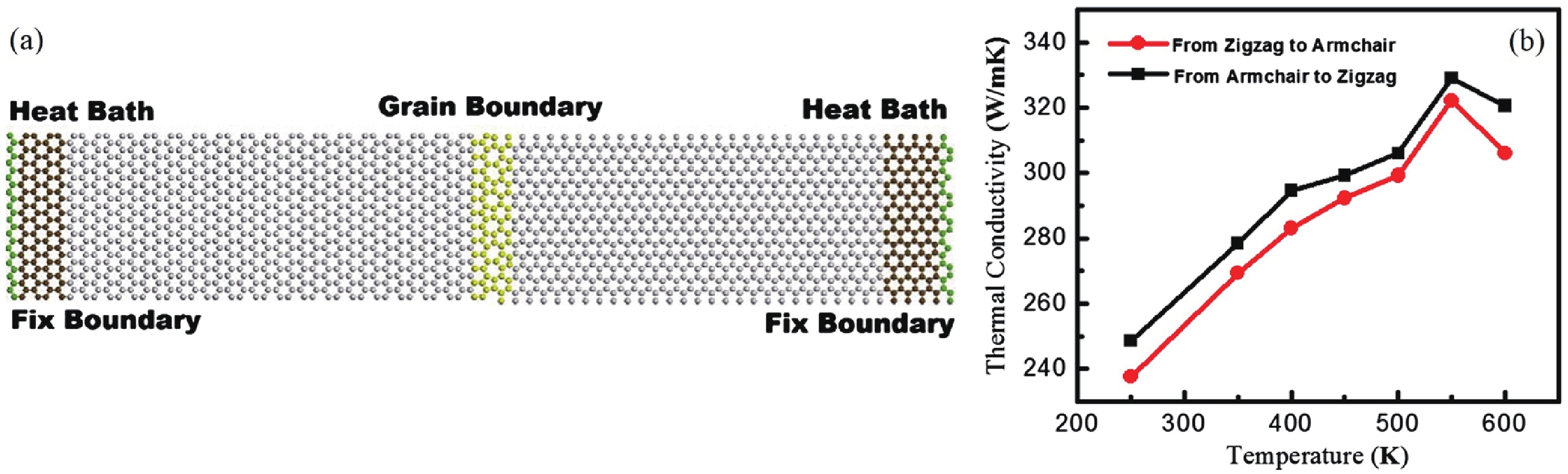
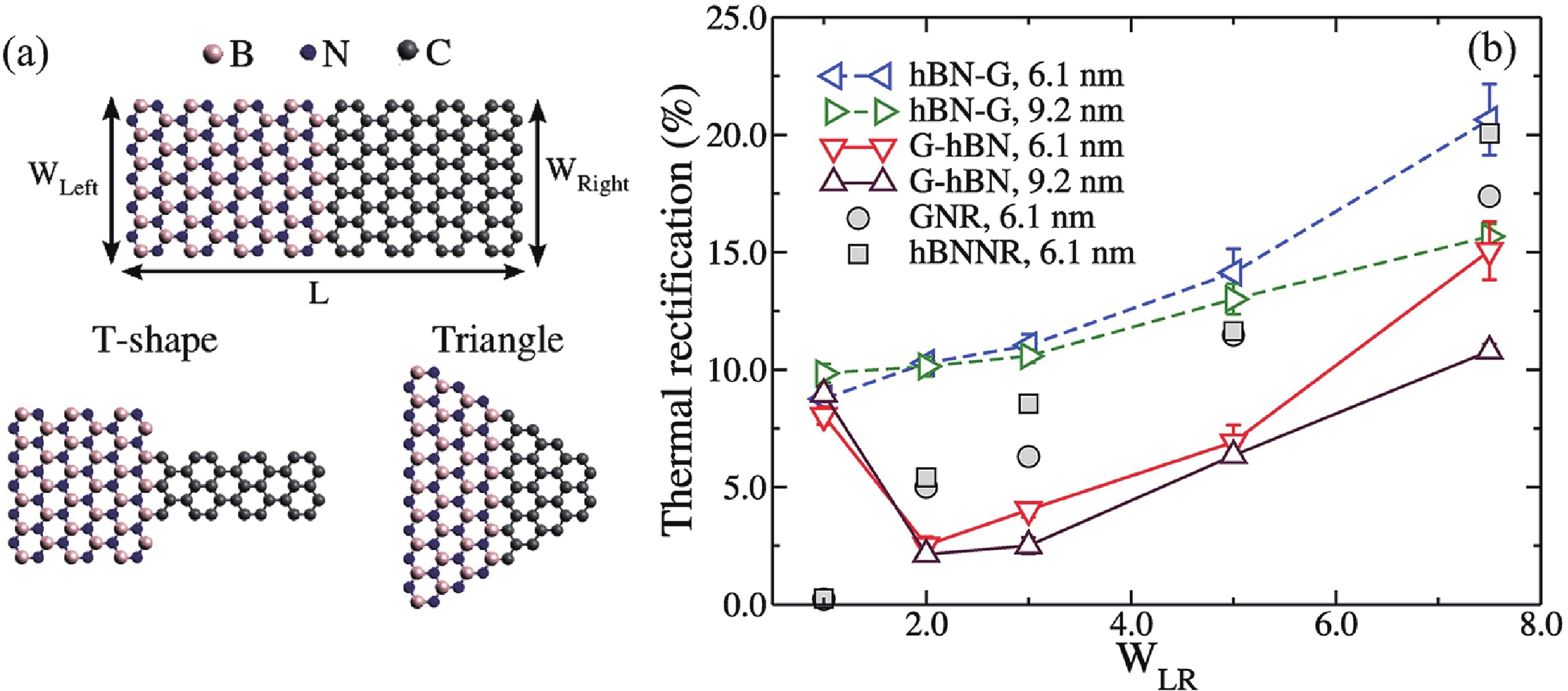
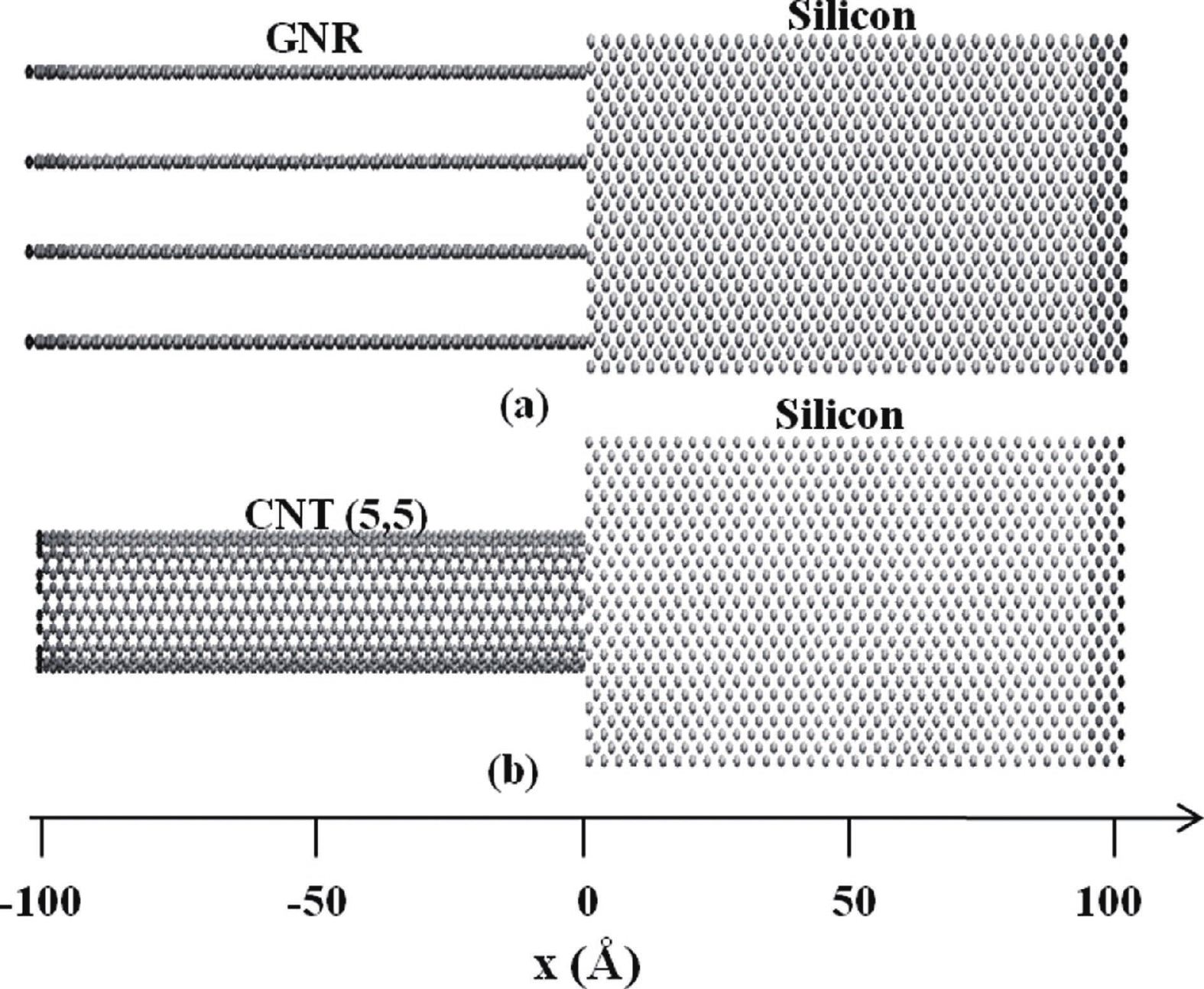
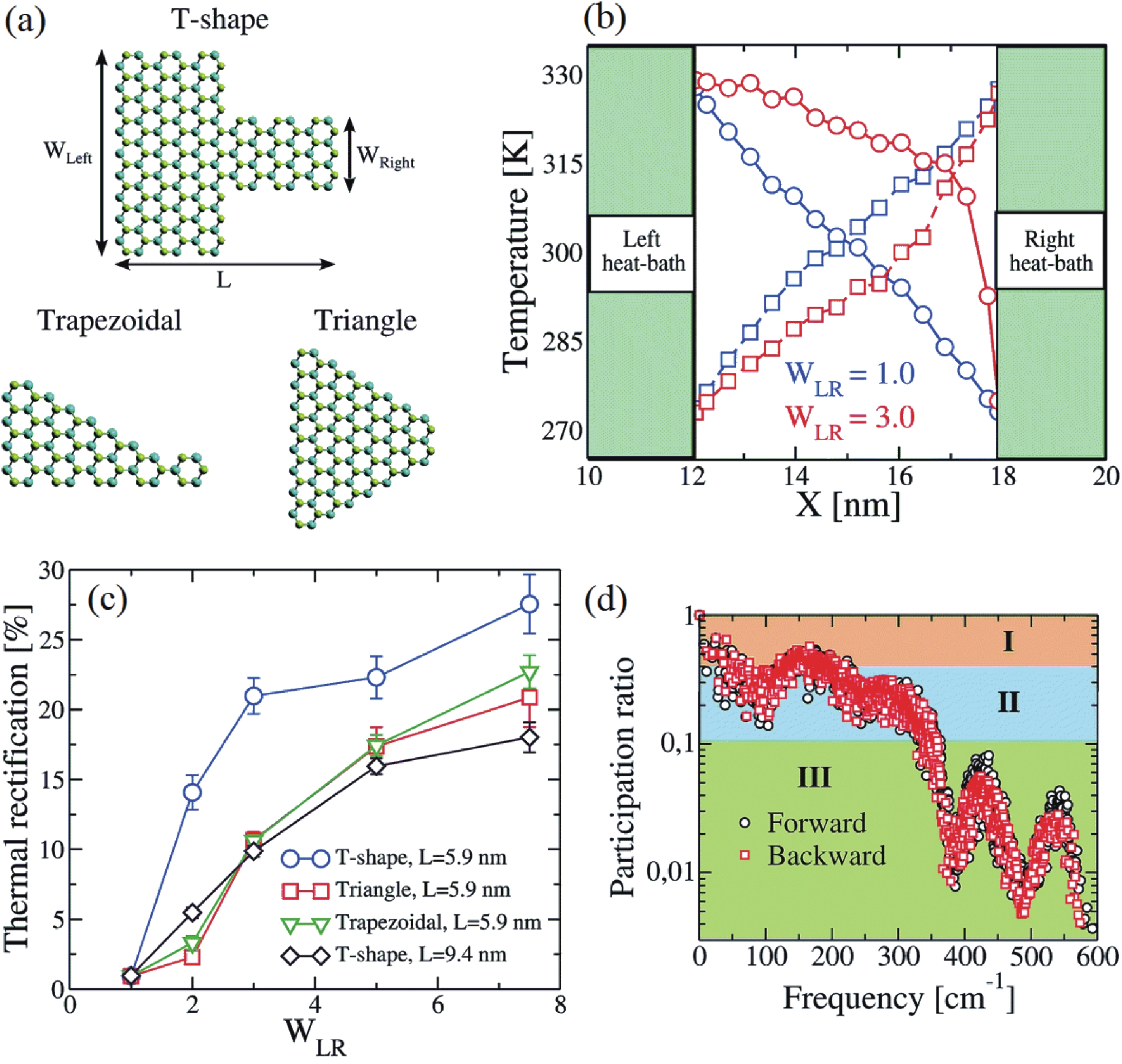
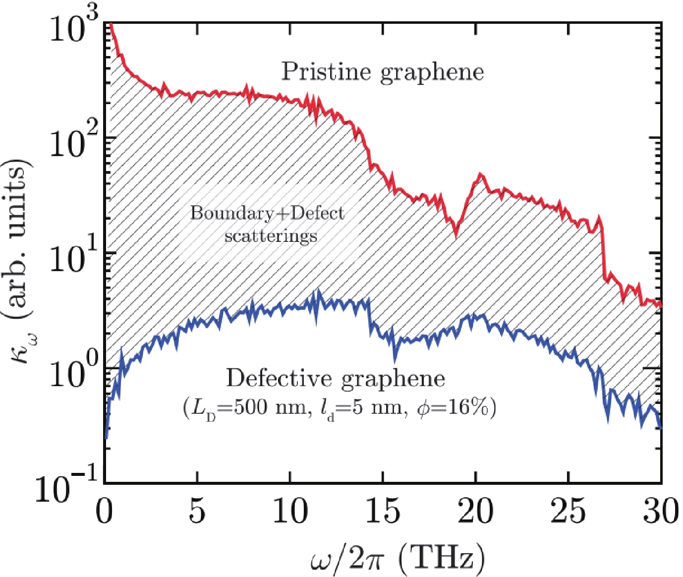
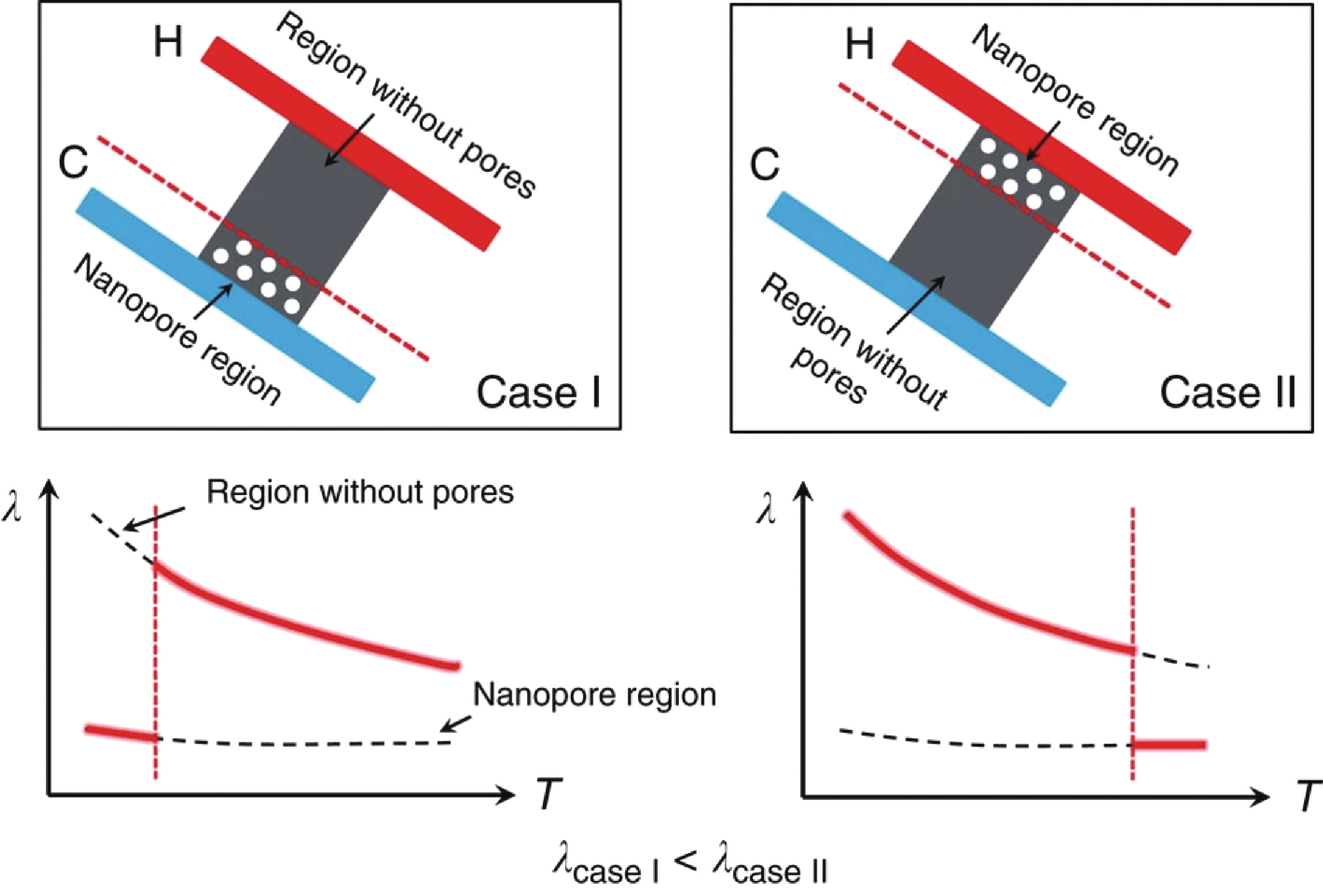
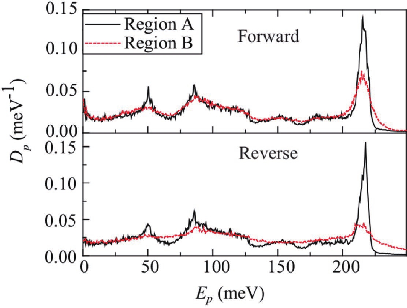
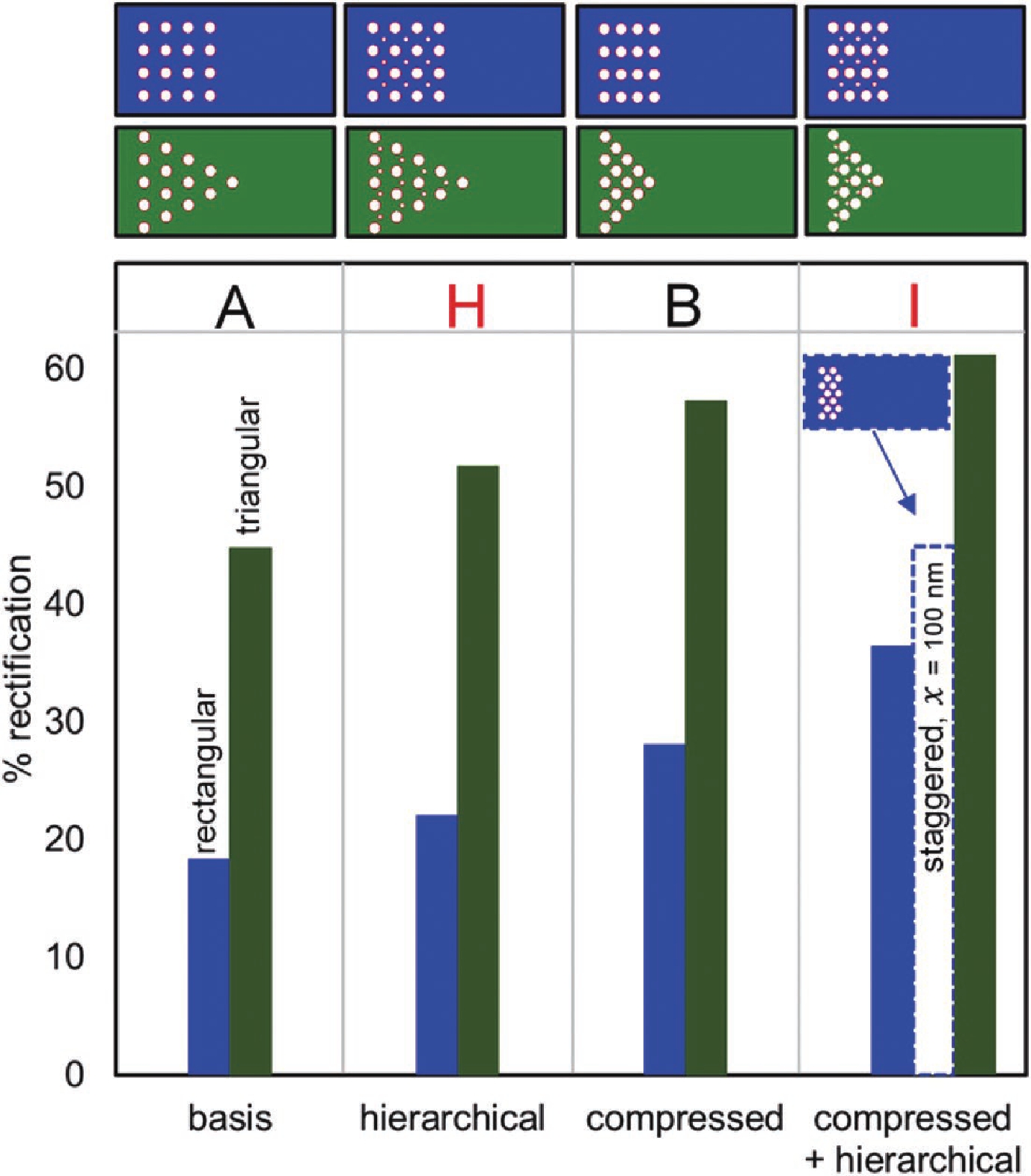
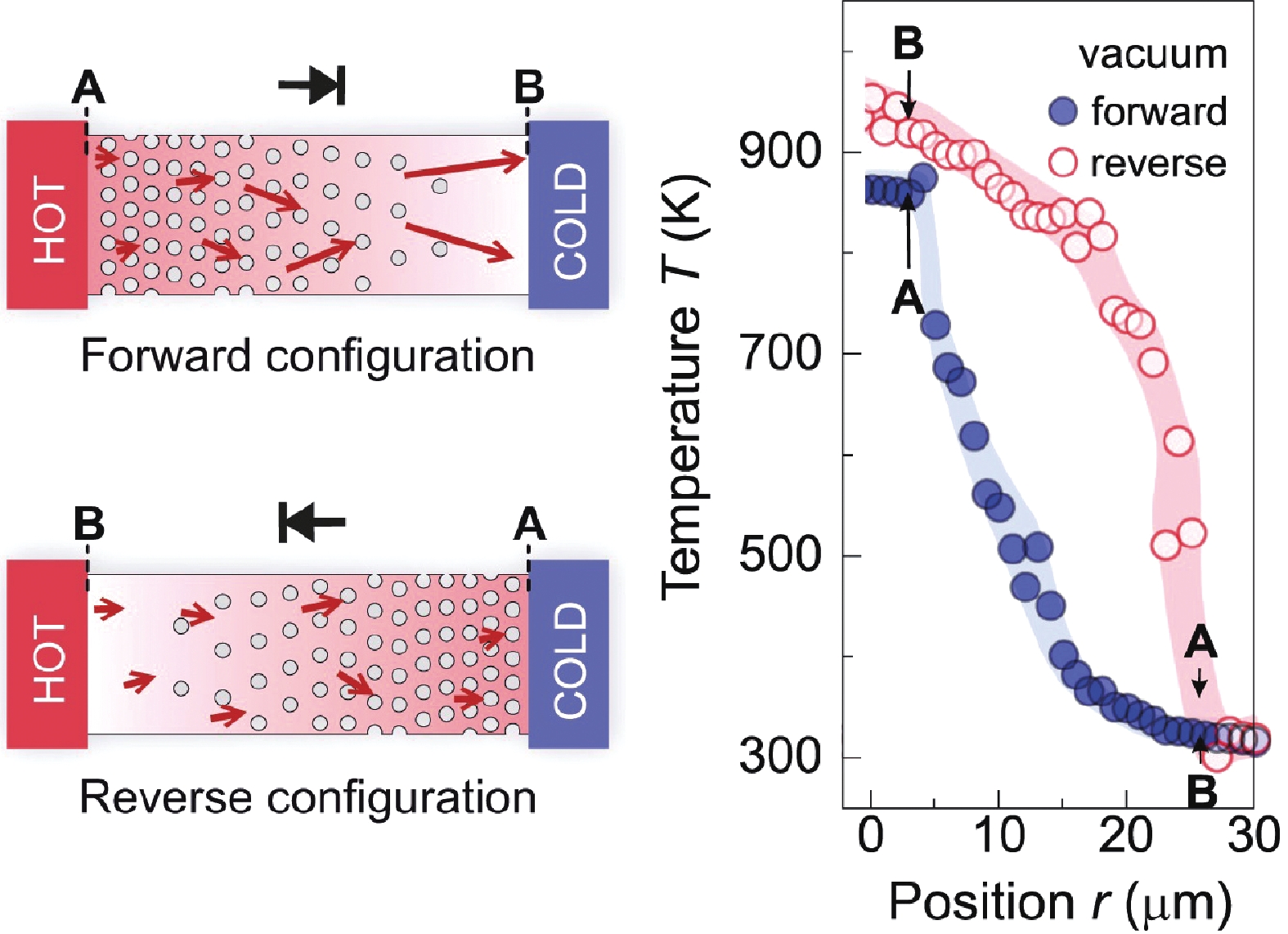
Thermal rectification, or the asymmetric transport of heat along a structure, has recently been investigated as a potential solution to the thermal management issues that accompany the miniaturization of electronic devices. Applications of this concept in thermal logic circuits analogous to existing electronics-based processor logic have also been proposed. This review highlights some of the techniques that have been recently investigated for their potential to induce asymmetric thermal conductivity in solid-state structures that are composed of materials of interest to the electronics industry. These rectification approaches are compared in terms of their quantitative performance, as well as the range of practical applications that they would be best suited to. Techniques applicable to a range of length scales, from the continuum regime to quantum dots, are discussed, and where available, experimental findings that build upon numerical simulations or analytical predictions are also highlighted.


J. Semicond.
2022, 43(10): 102002 doi: 10.1088/1674-4926/43/10/102002
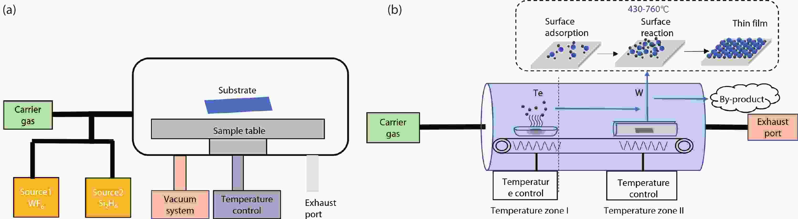
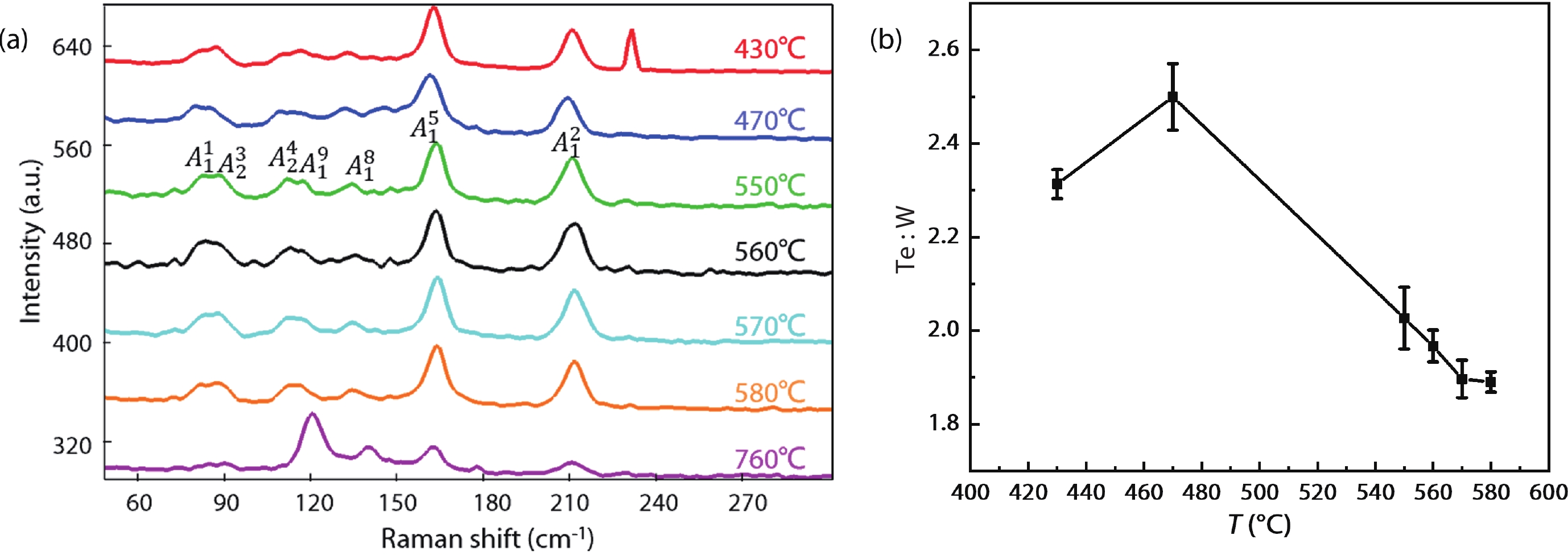
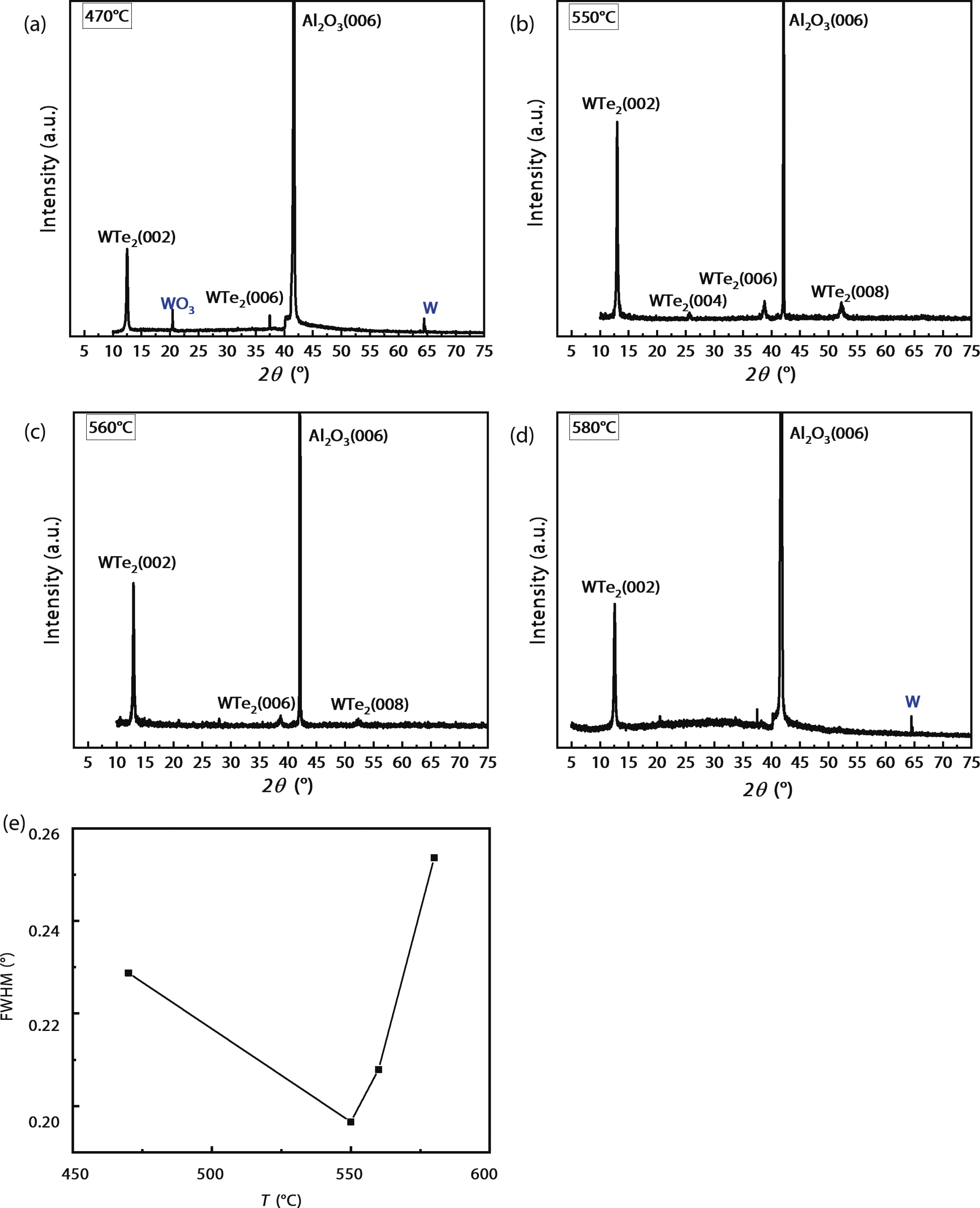
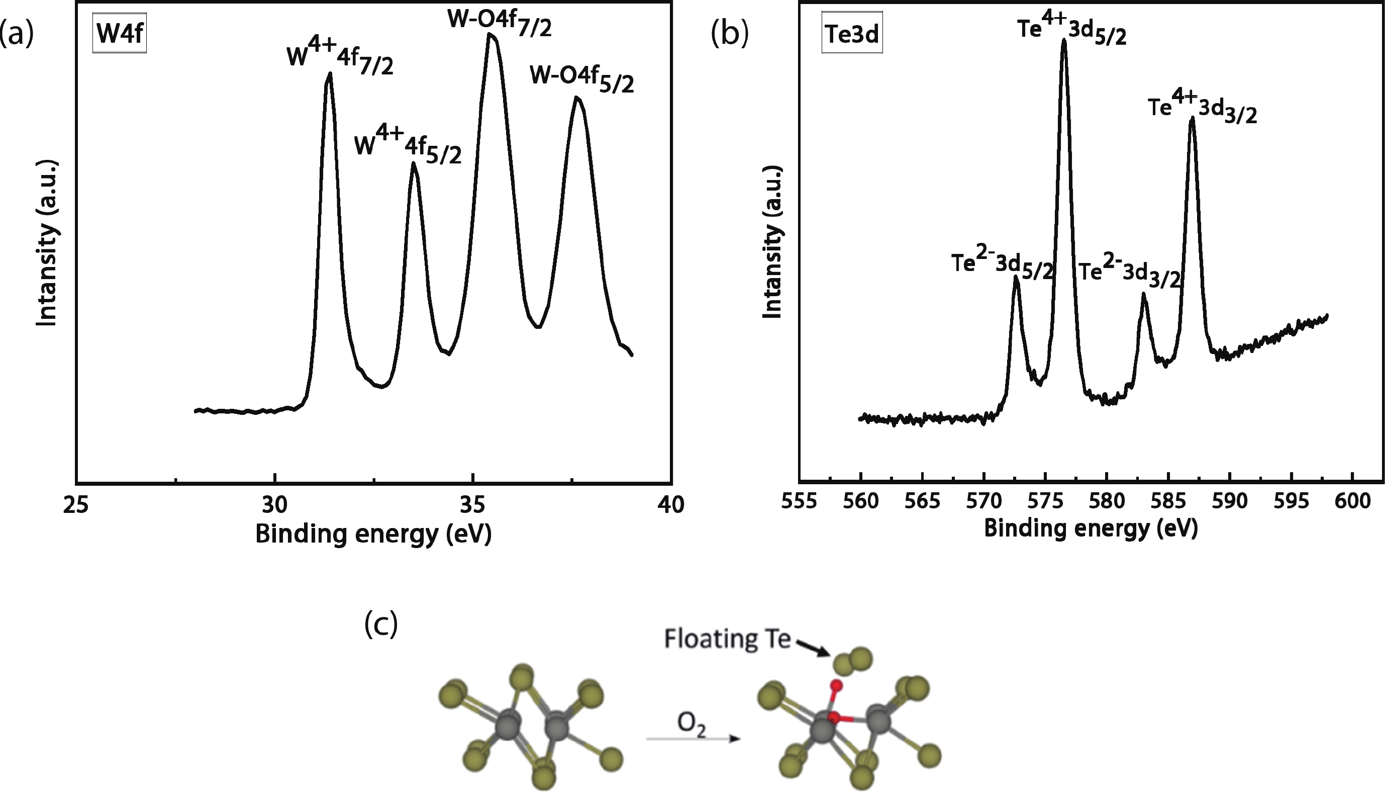
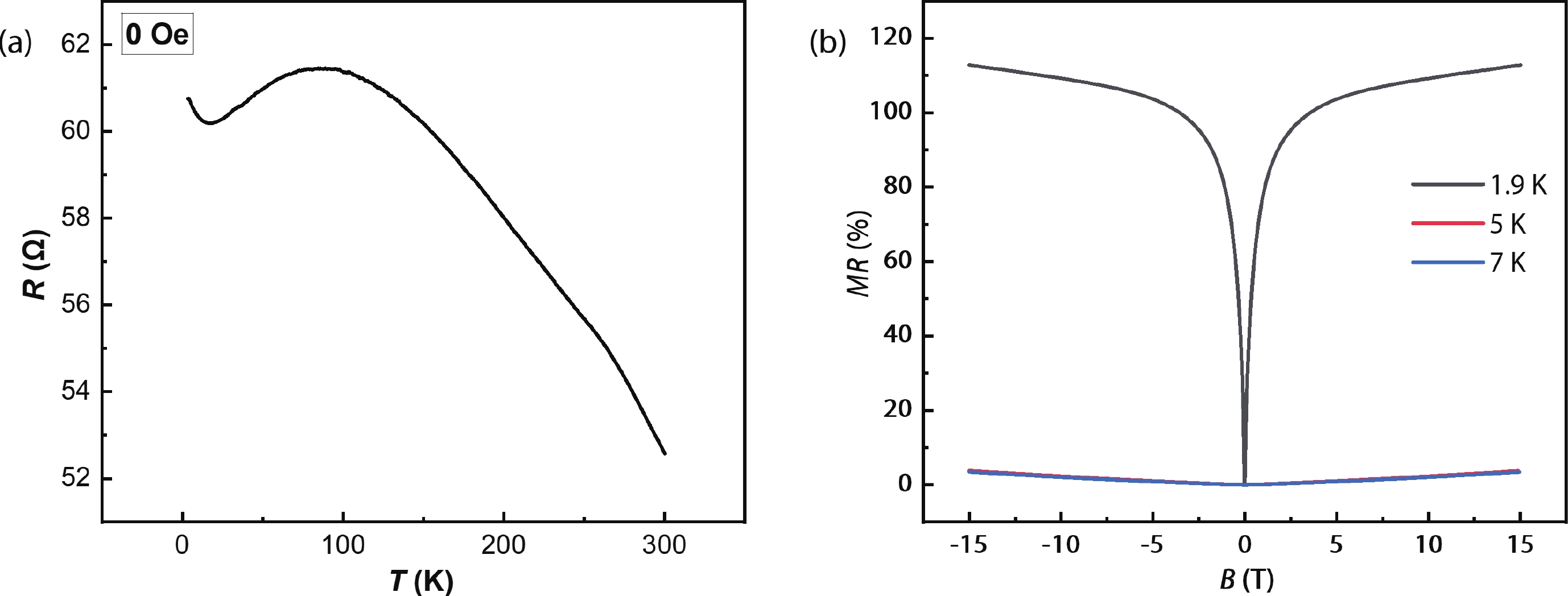
Tungsten telluride thin films were successfully prepared on monocrystal sapphire substrates by using atomic layer deposition and chemical vapor deposition technology, and the effects of different tellurization temperatures on the properties of tungsten telluride films were investigated. The growth rate, crystal structure and composition of the film samples were characterized and analyzed by using scanning electron microscope, Raman spectroscopy and X-ray photoelectron spectroscopy. The results showed that tungsten telluride thin films with good crystal orientation in (001) were obtained at telluride temperature of 550 °C. When the telluride temperature reached 570 °C, the tungsten telluride began to decompose and unsaturated magnetoresistance was found.


J. Semicond.
2022, 43(10): 102301 doi: 10.1088/1674-4926/43/10/102301
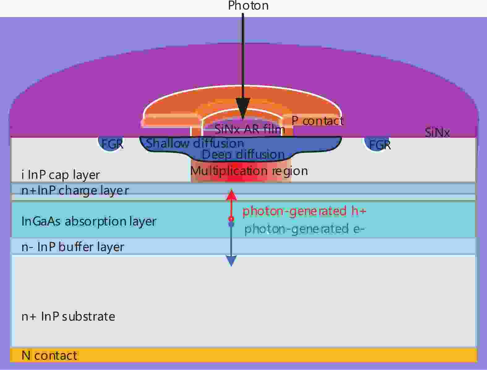
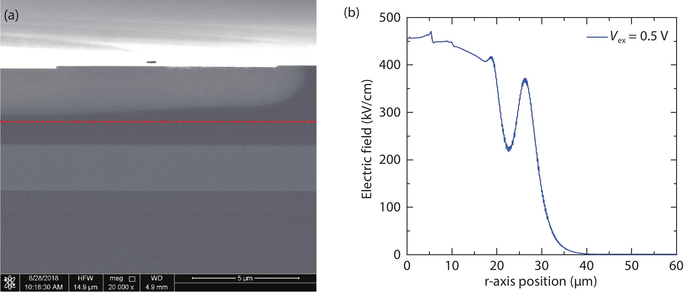
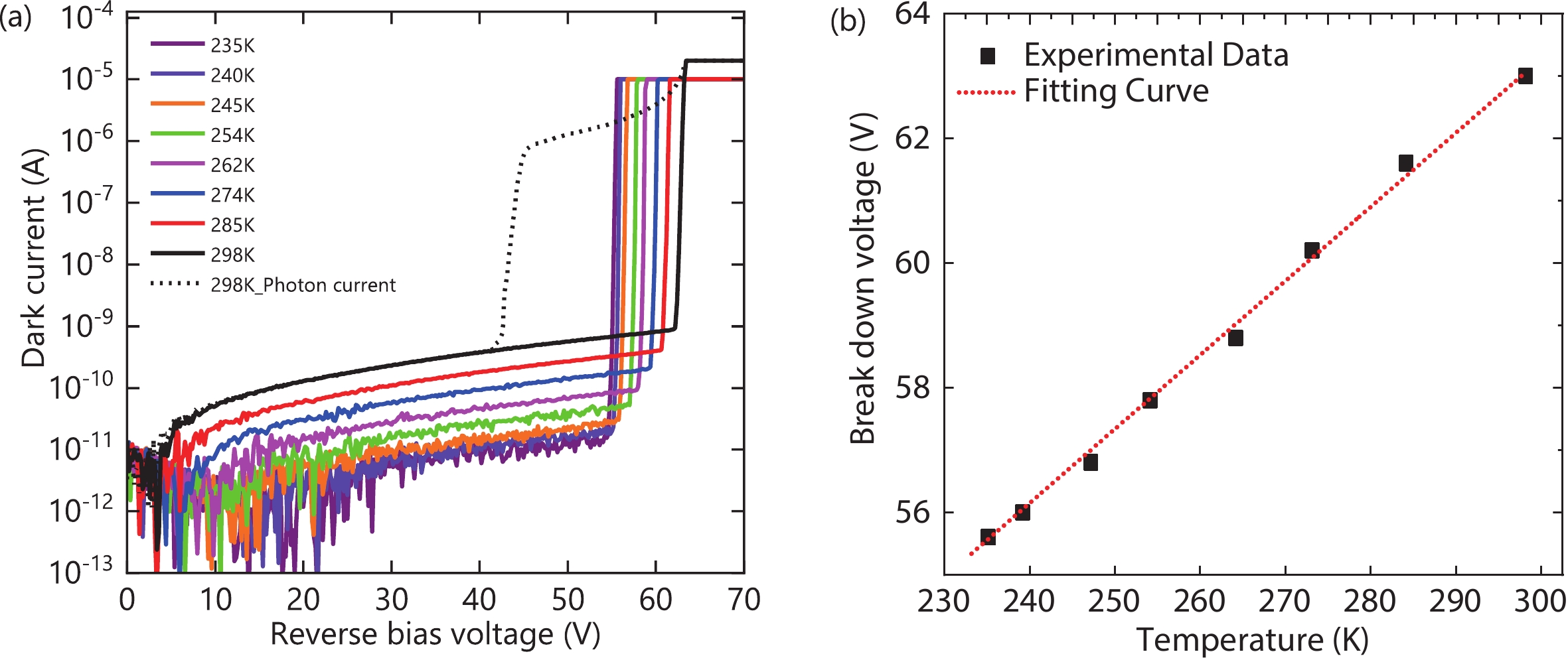
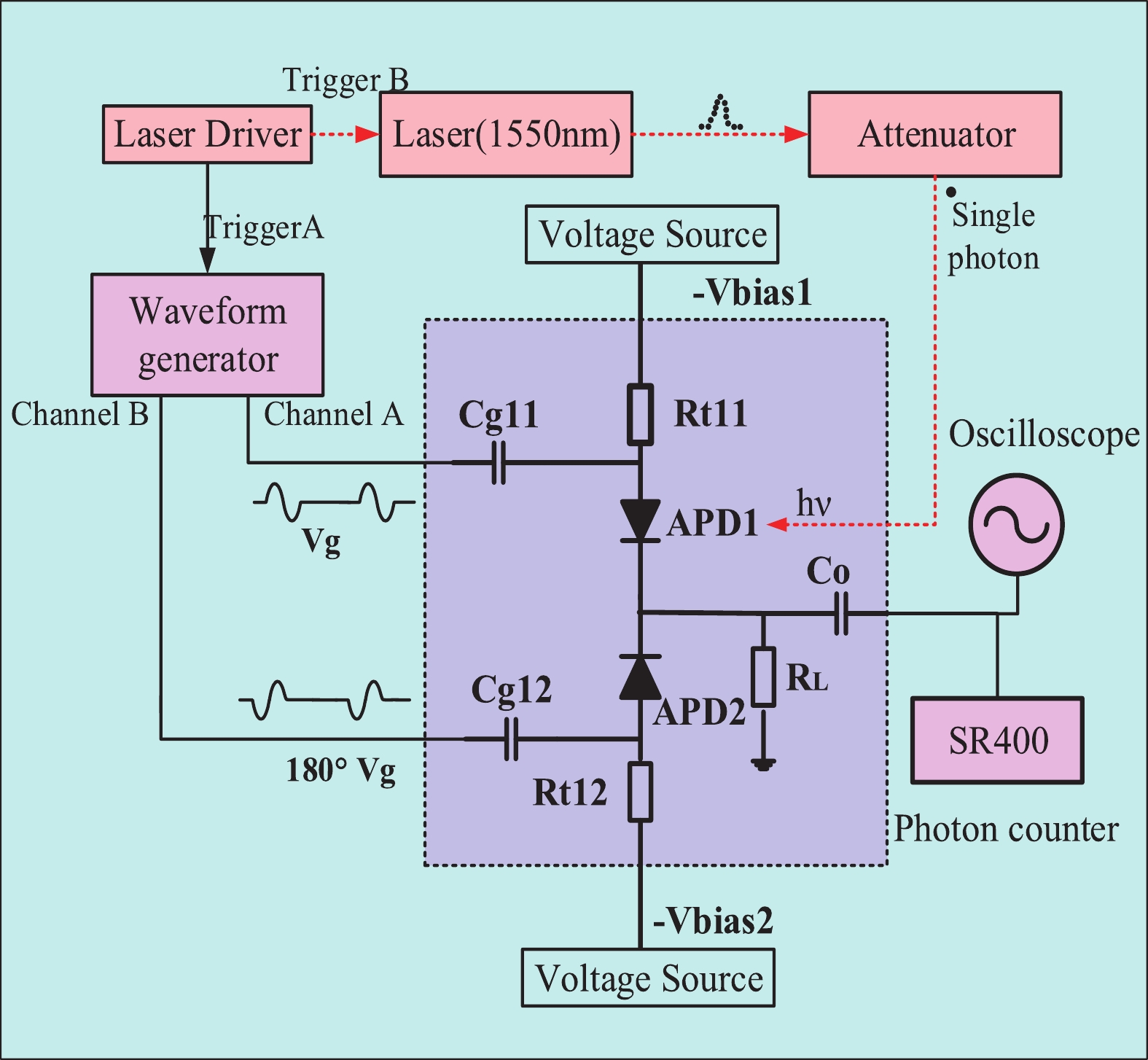
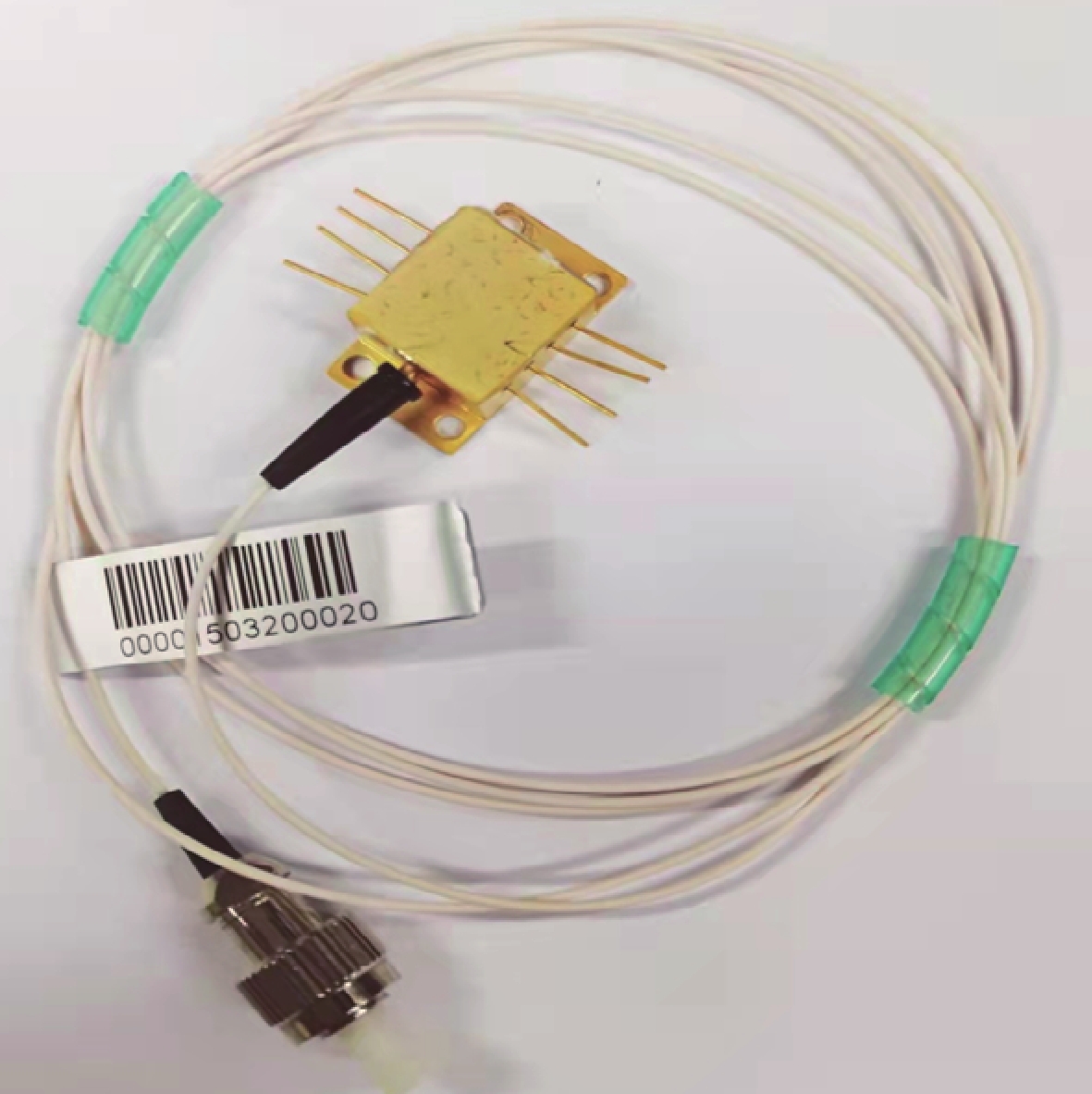
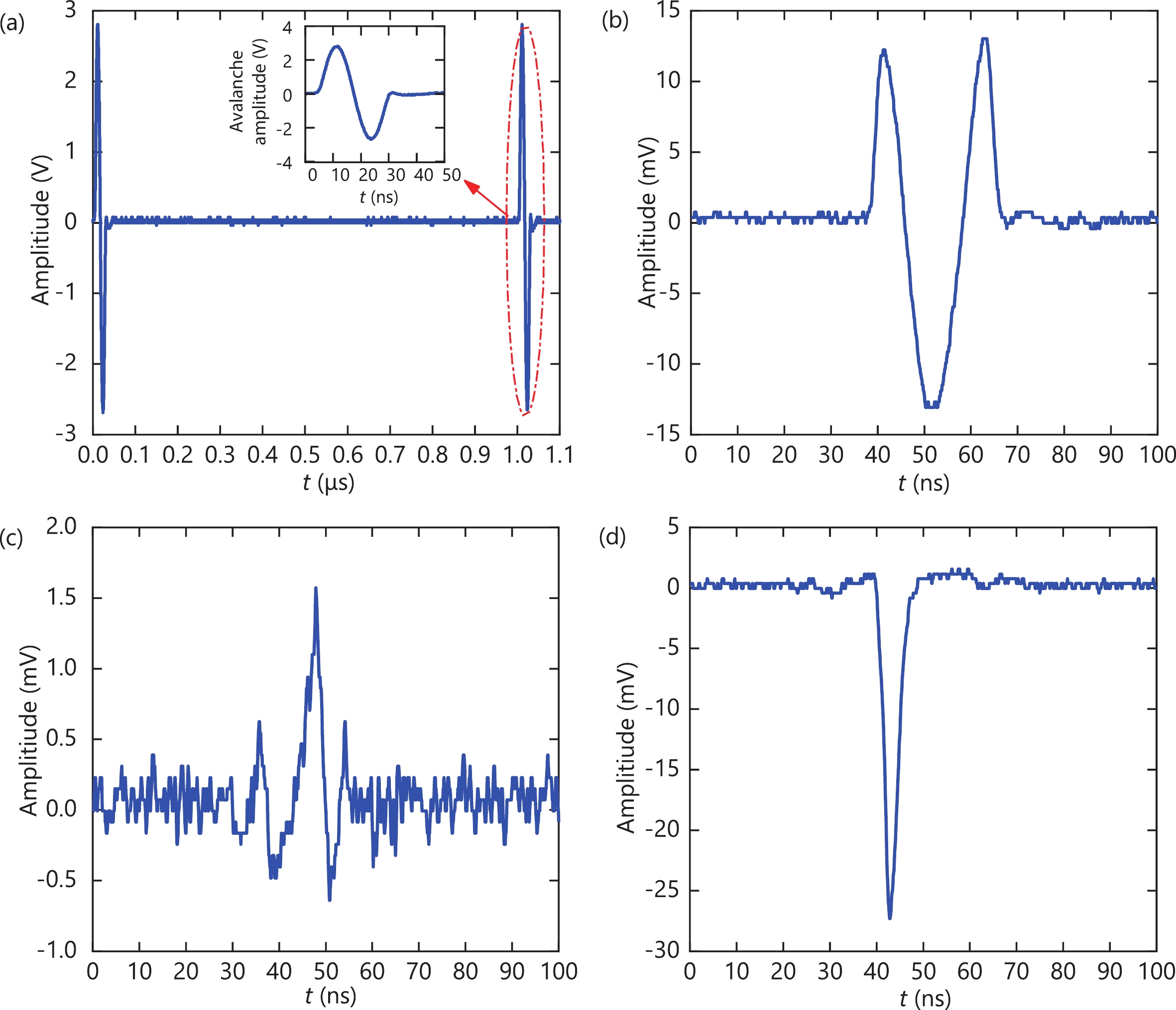
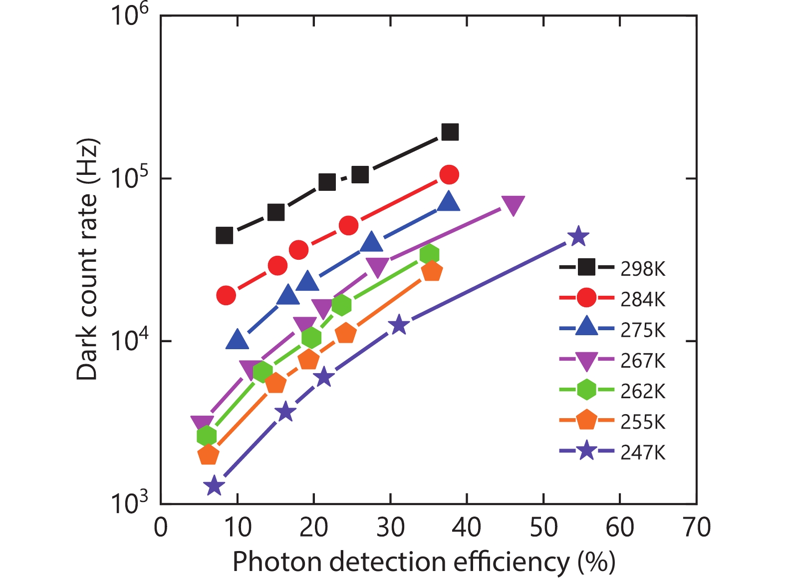
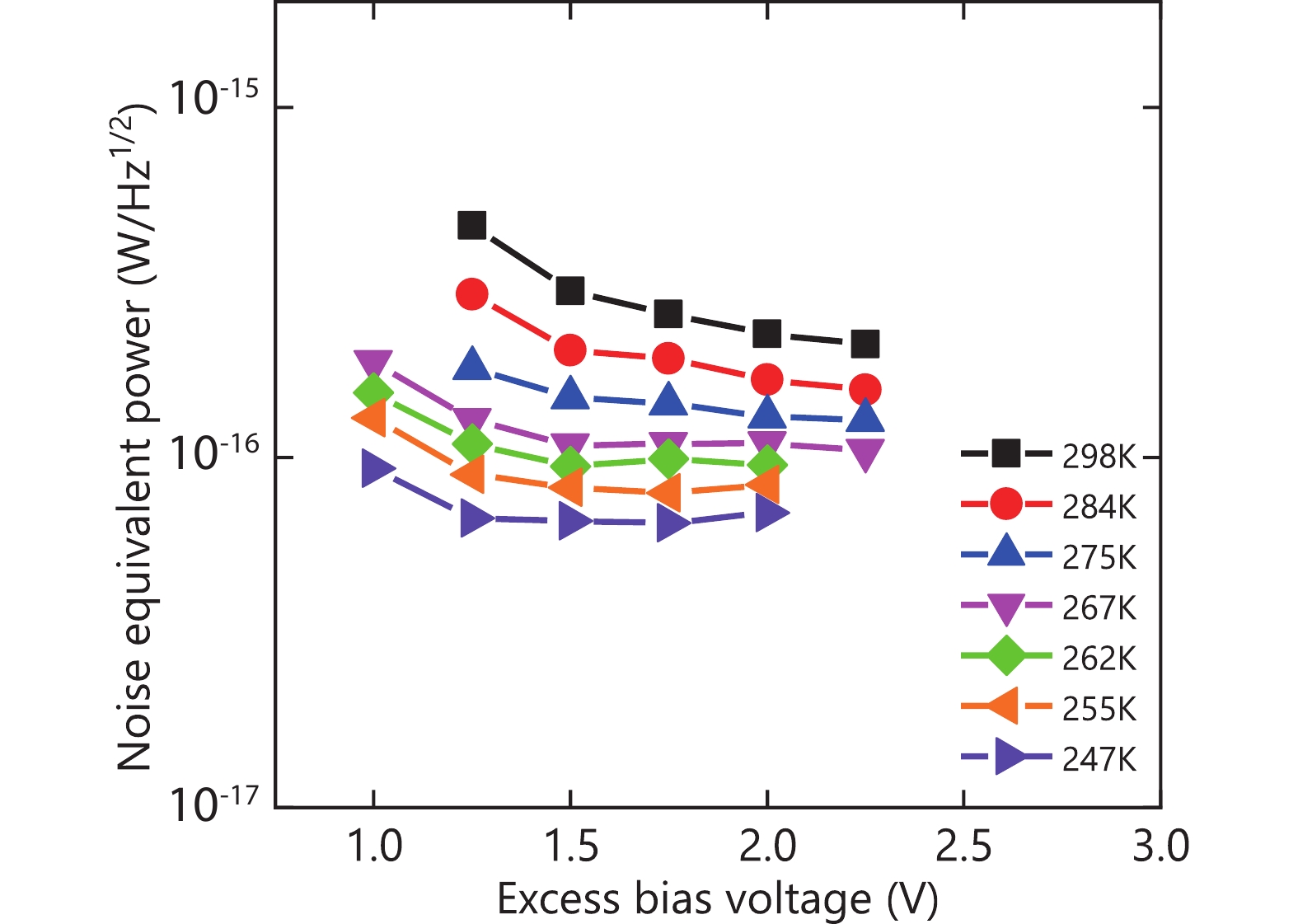
Planar semiconductor InGaAs/InP single photon avalanche diodes with high responsivity and low dark count rate are preferred single photon detectors in near-infrared communication. However, even with well-designed structures and well-controlled operational conditions, the performance of InGaAs/InP SPADs is limited by the inherent characteristics of avalanche process and the growth quality of InGaAs/InP materials. It is difficult to ensure high detection efficiency while the dark count rate is controlled within a certain range at present. In this paper, we fabricated a device with a thick InGaAs absorption region and an anti-reflection layer. The quantum efficiency of this device reaches 83.2%. We characterized the single-photon performance of the device by a quenching circuit consisting of parallel-balanced InGaAs/InP single photon detectors and single-period sinusoidal pulse gating. The spike pulse caused by the capacitance effect of the device is eliminated by using the characteristics of parallel balanced common mode signal elimination, and the detection of small avalanche pulse amplitude signal is realized. The maximum detection efficiency is 55.4% with a dark count rate of 43.8 kHz and a noise equivalent power of 6.96 × 10⁻¹⁷ W/Hz1/2 at 247 K. Compared with other reported detectors, this SPAD exhibits higher SPDE and lower noise-equivalent power at a higher cooling temperature.


J. Semicond.
2022, 43(10): 102501 doi: 10.1088/1674-4926/43/10/102501
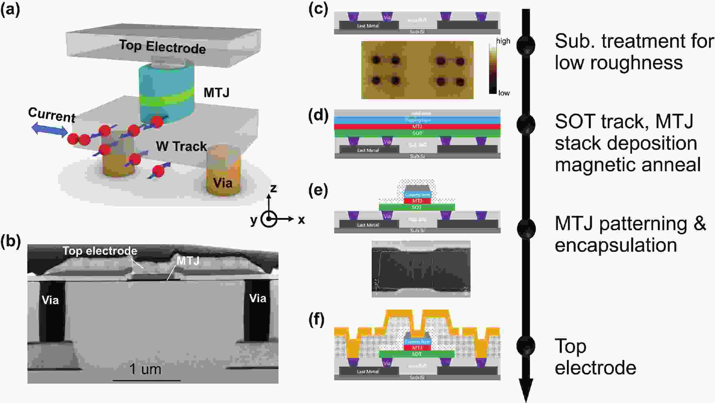
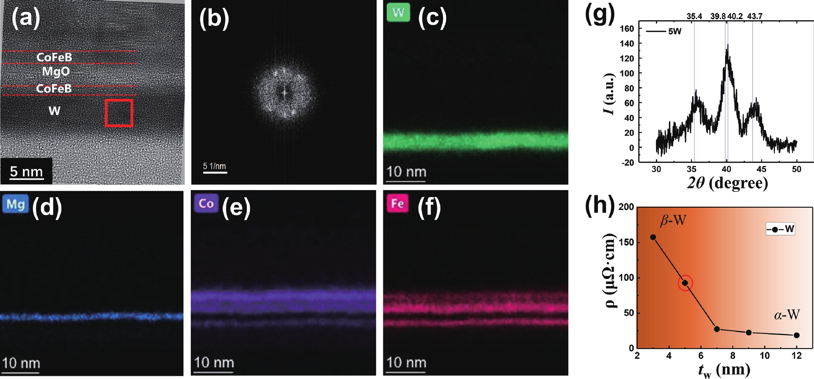
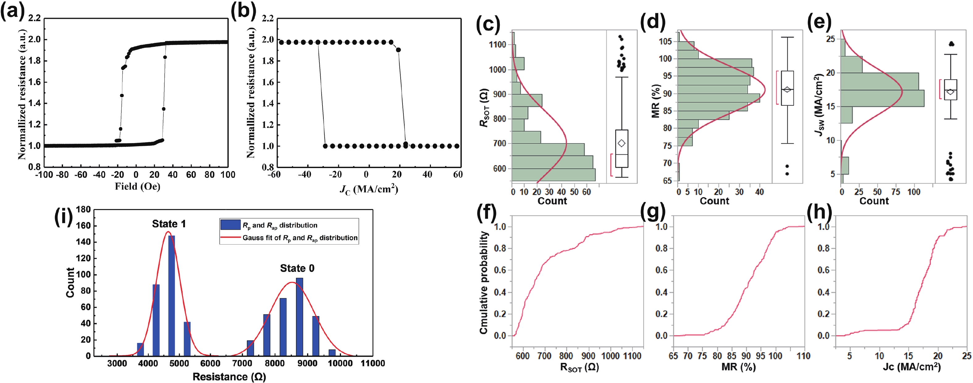
We demonstrate in-plane field-free-switching spin-orbit torque (SOT) magnetic tunnel junction (MTJ) devices that are capable of low switching current density, fast speed, high reliability, and, most importantly, manufactured uniformly by the 200-mm-wafer platform. The performance of the devices is systematically studied, including their magnetic properties, switching behaviors, endurance and data retention. The successful integration of SOT devices within the 200-mm-wafer manufacturing platform provides a feasible way to industrialize SOT MRAMs. It is expected to obtain excellent performance of the devices by further optimizing the MTJ film stacks and the corresponding fabrication processes in the future.


J. Semicond.
2022, 43(10): 102801 doi: 10.1088/1674-4926/43/10/102801
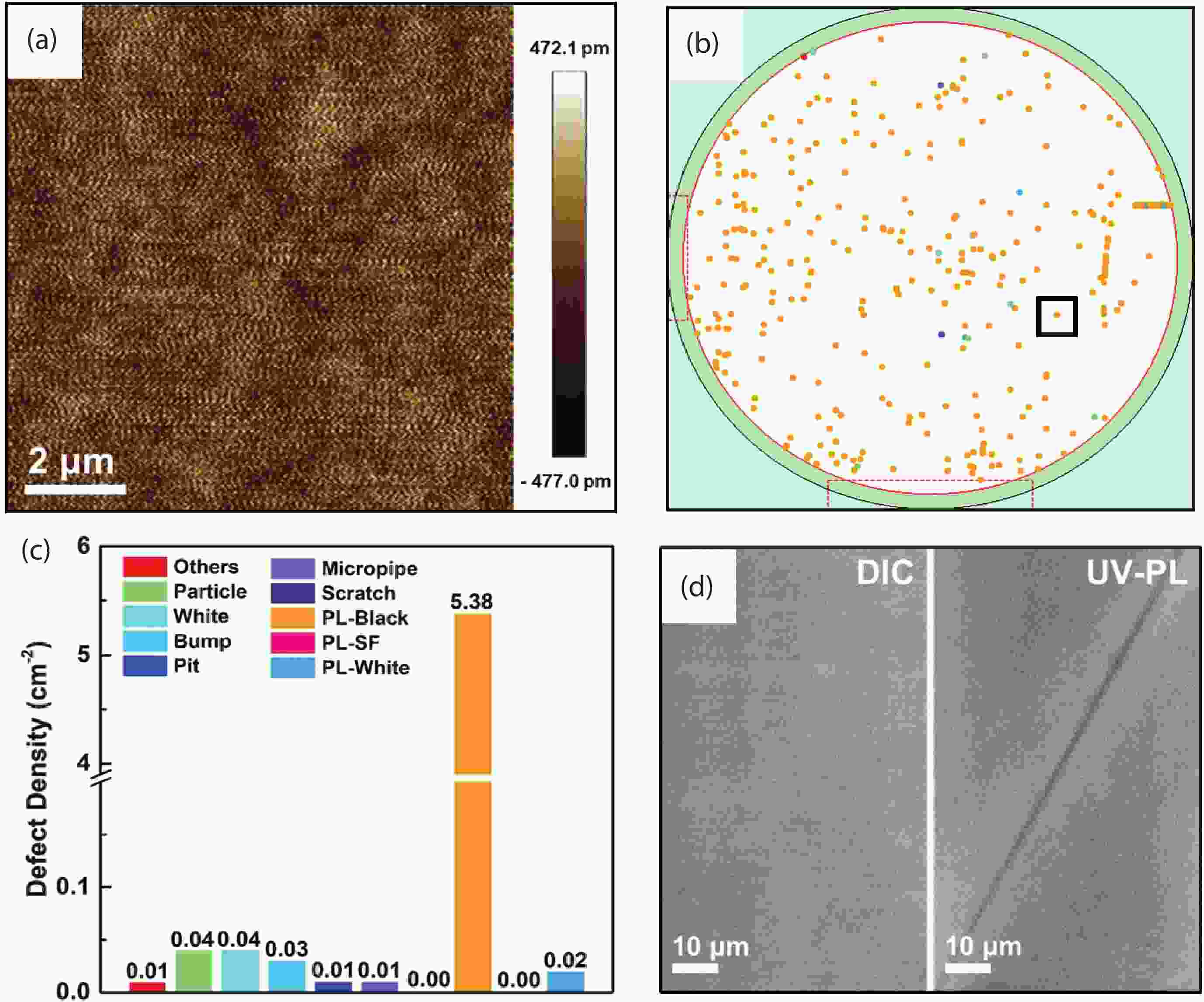
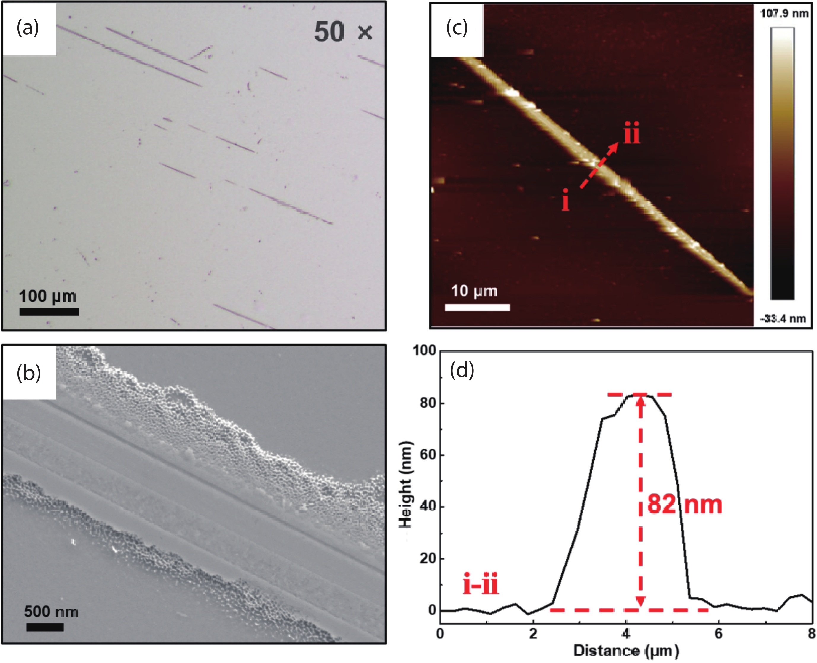
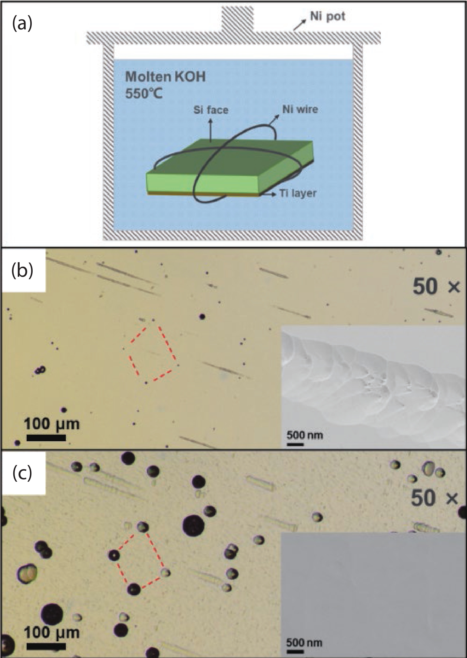
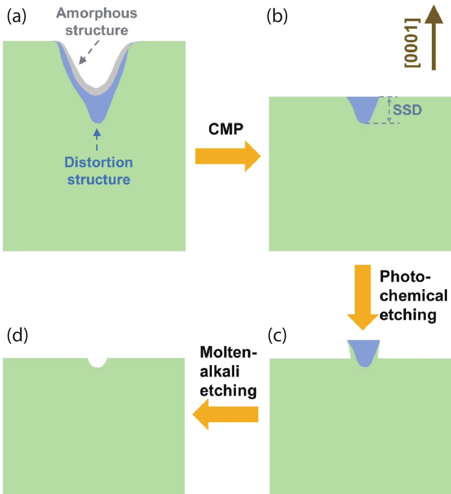
In this work, we propose to reveal the subsurface damage (SSD) of 4H-SiC wafers by photo-chemical etching and identify the nature of SSD by molten-alkali etching. Under UV illumination, SSD acts as a photoluminescence-black defect. The selective photo-chemical etching reveals SSD as the ridge-like defect. It is found that the ridge-like SSD is still crystalline 4H-SiC with lattice distortion. The molten-KOH etching of the 4H-SiC wafer with ridge-like SSD transforms the ridge-like SSD into groove lines, which are typical features of scratches. This means that the underlying scratches under mechanical stress give rise to the formation of SSD in 4H-SiC wafers. SSD is incorporated into 4H-SiC wafers during the lapping, rather than the chemical mechanical polishing (CMP).


J. Semicond.
2022, 43(10): 104101 doi: 10.1088/1674-4926/43/10/104101
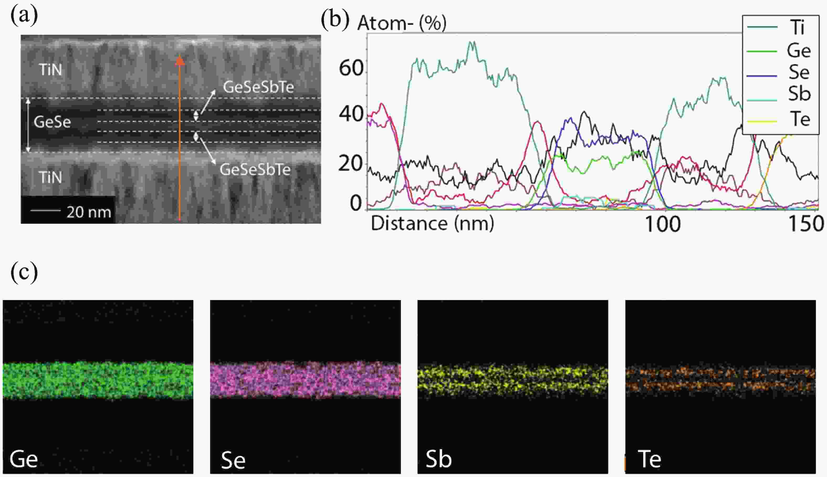
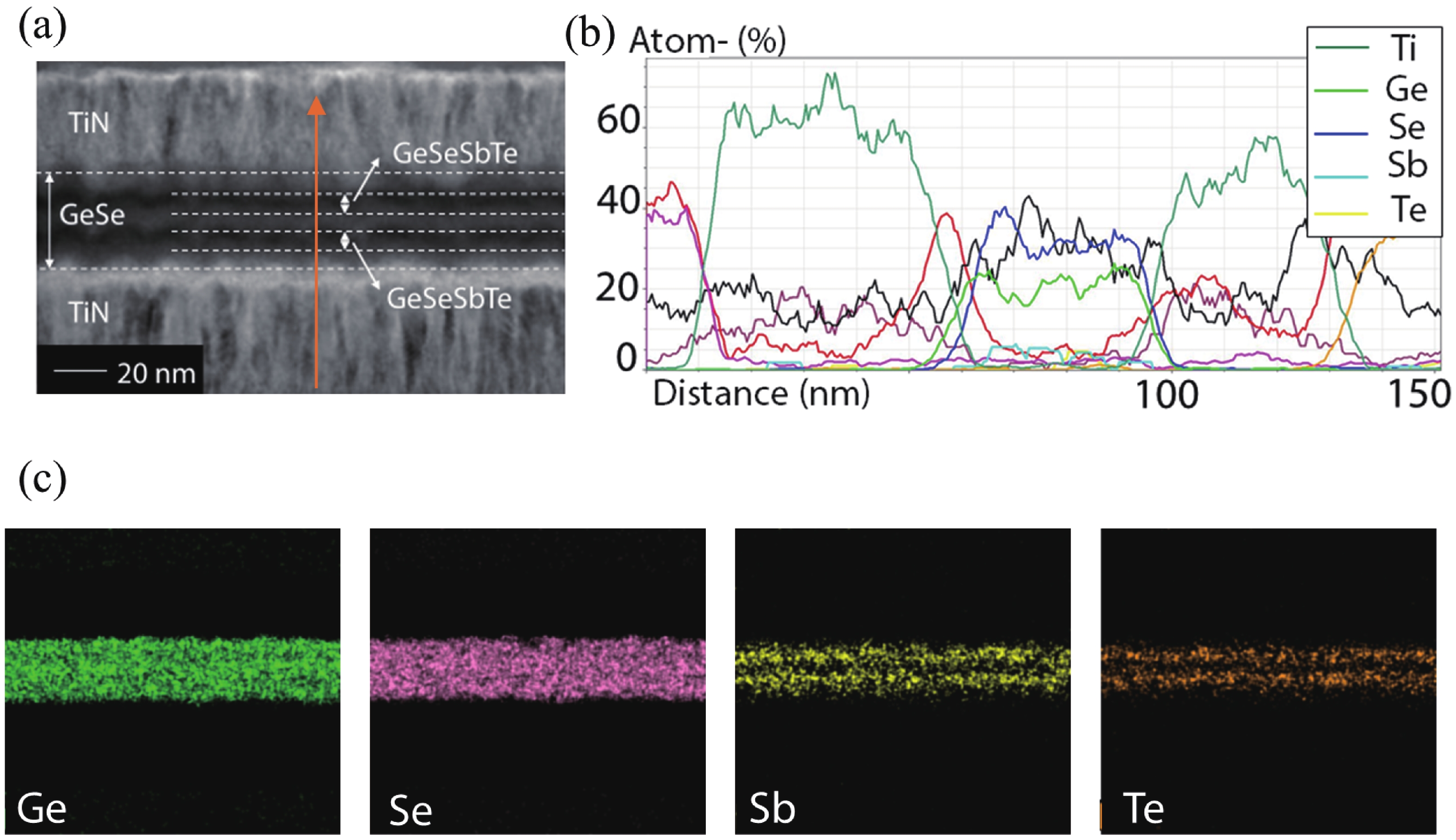
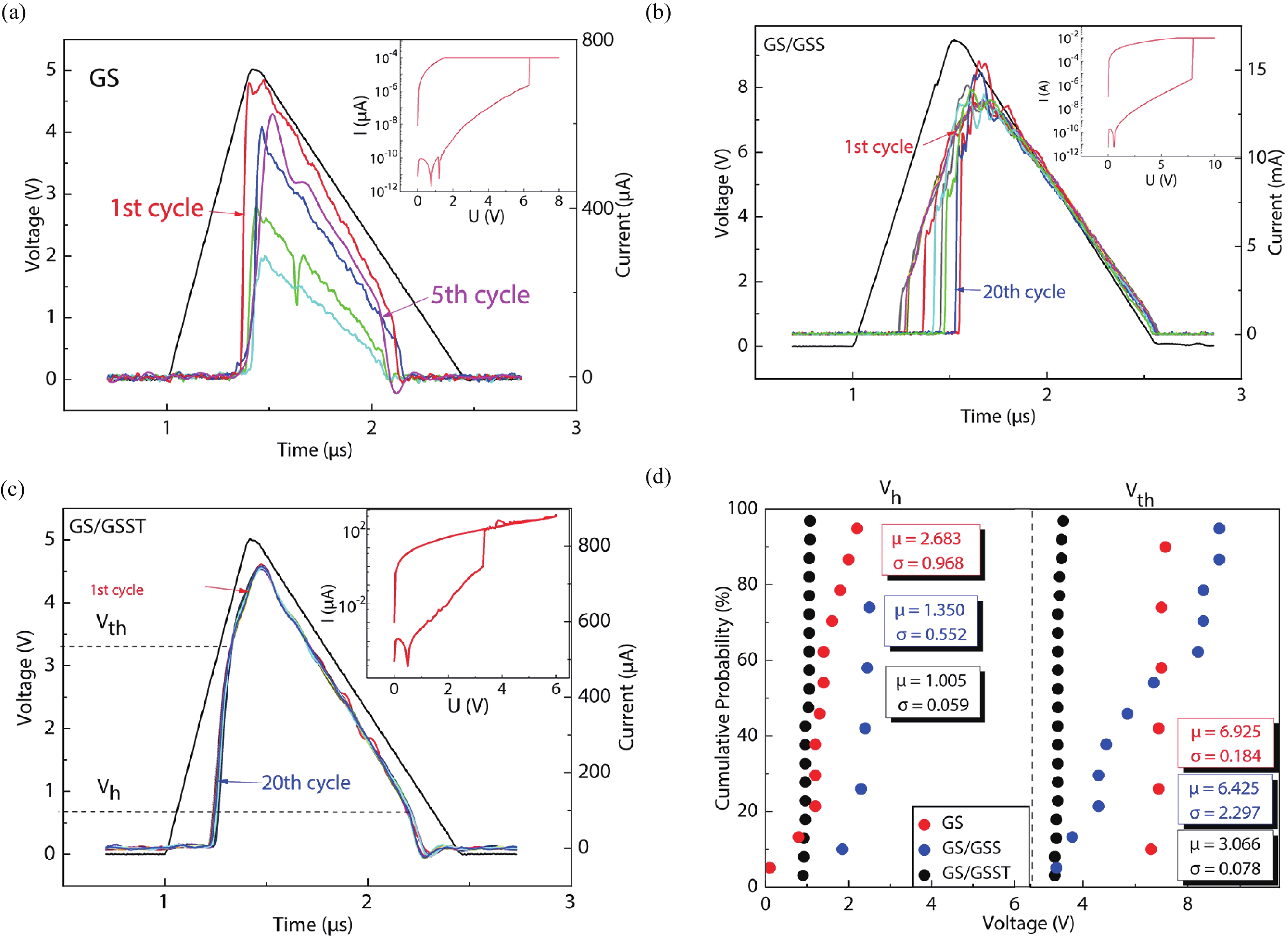
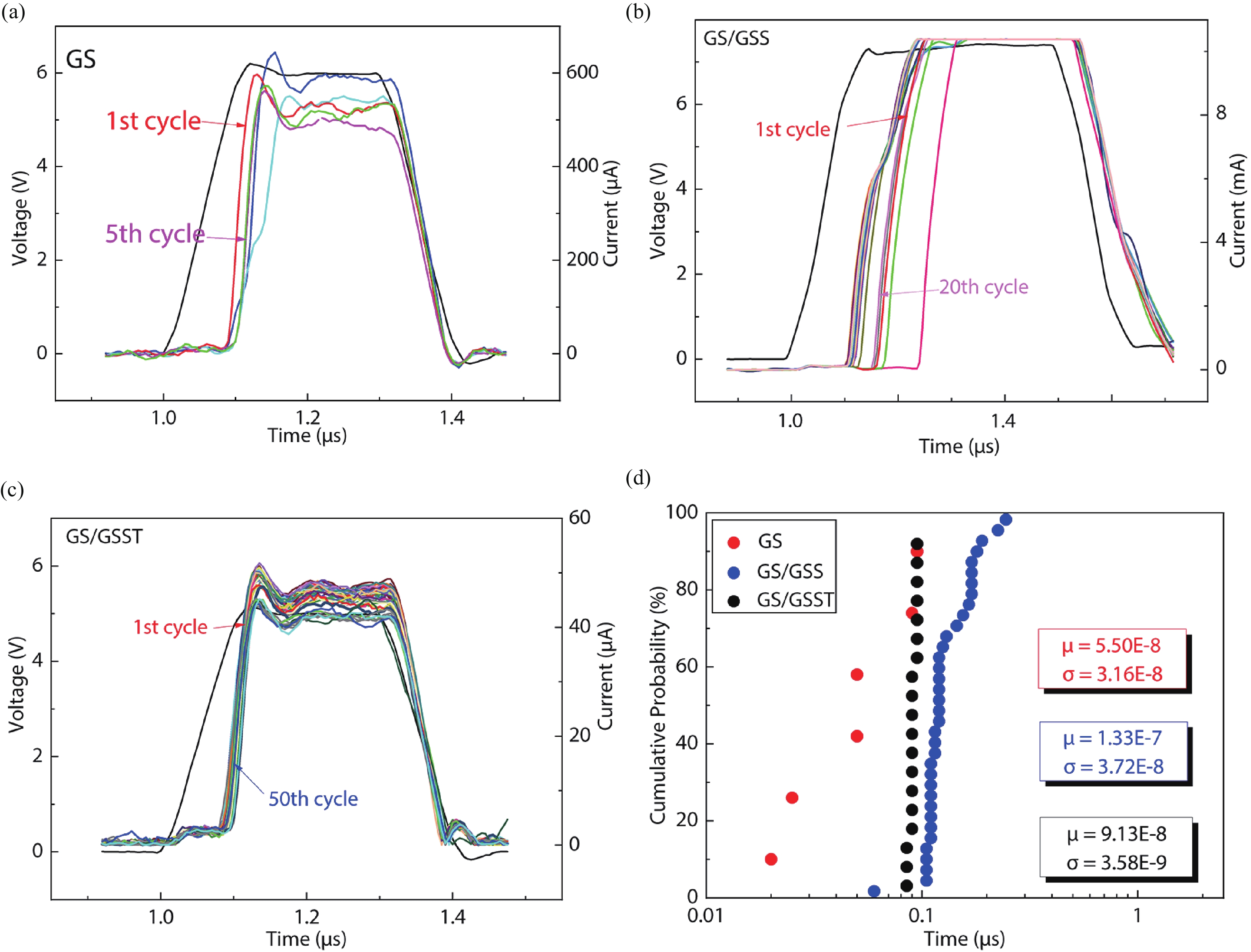
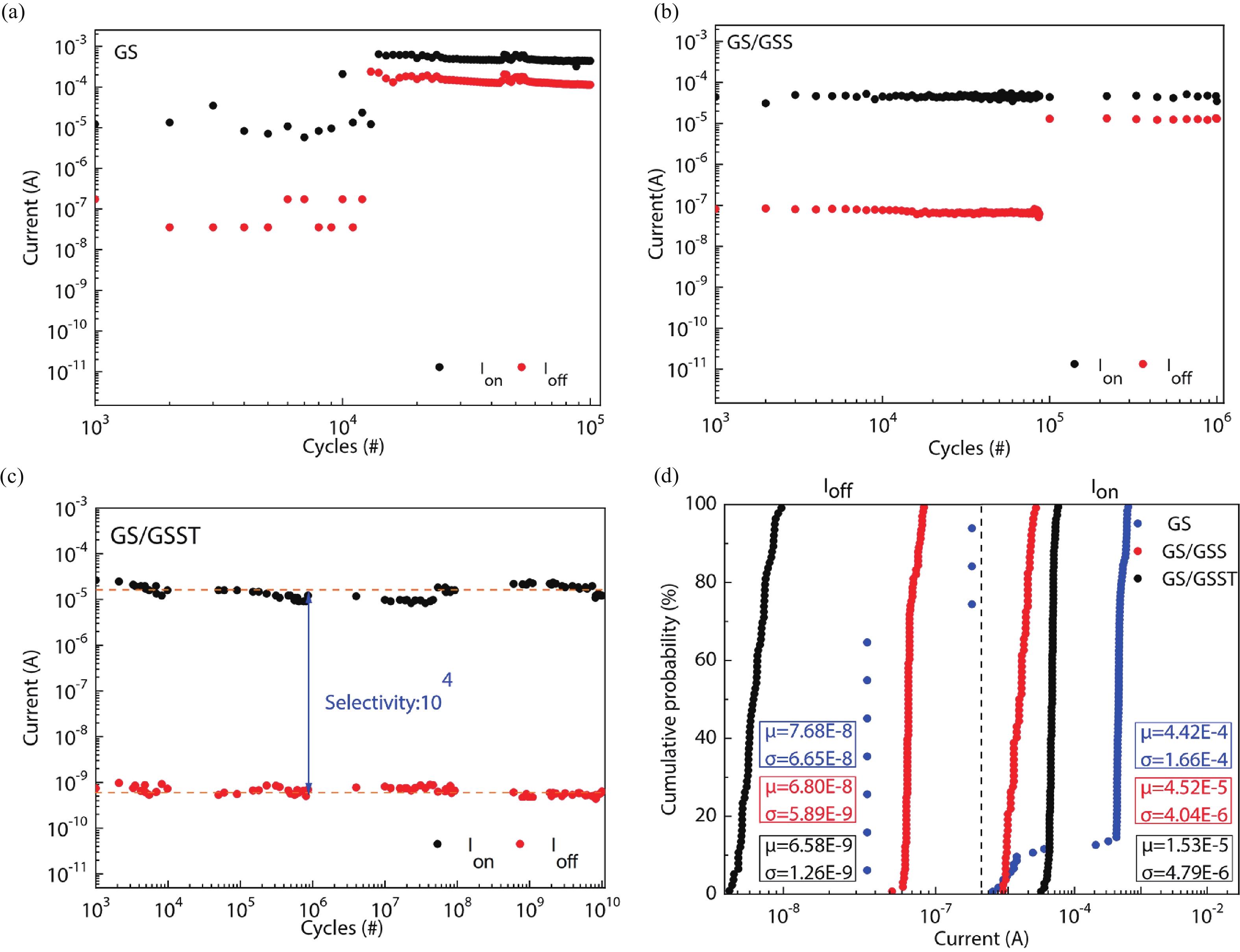
Selector devices are indispensable components of large-scale memristor array systems. The thereinto, ovonic threshold switching (OTS) selector is one of the most suitable candidates for selector devices, owing to its high selectivity and scalability. However, OTS selectors suffer from poor endurance and stability which are persistent tricky problems for application. Here, we report on a multilayer OTS selector based on simple GeSe and doped-GeSe. The experimental results show improving selector performed extraordinary endurance up to 1010 and the fluctuation of threshold voltage is 2.5%. The reason for the improvement may lie in more interface states which strengthen the interaction among individual layers. These developments pave the way towards tuning a new class of OTS materials engineering, ensuring improvement of electrical performance.
J. Semicond.
2022, 43(10): 104102 doi: 10.1088/1674-4926/43/10/104102
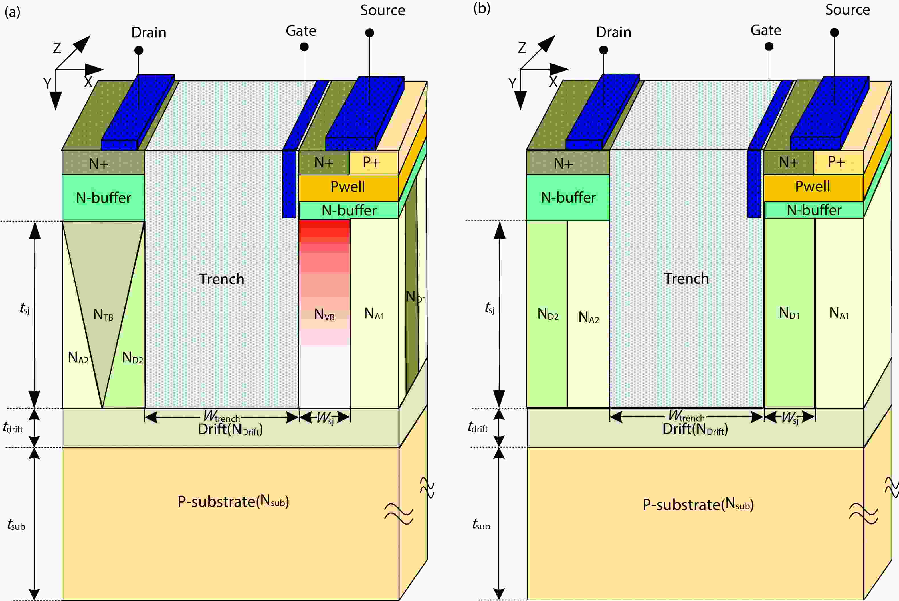
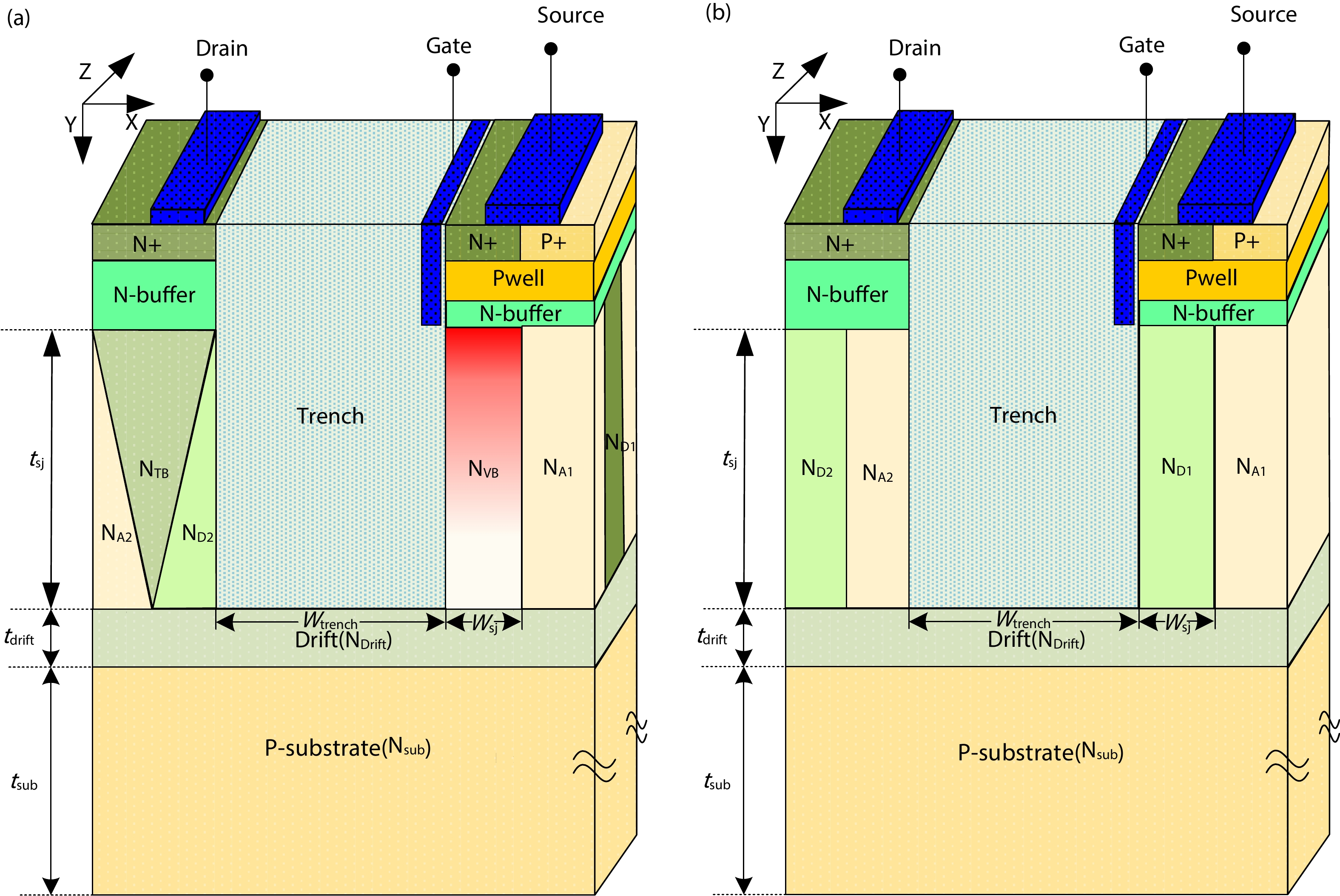
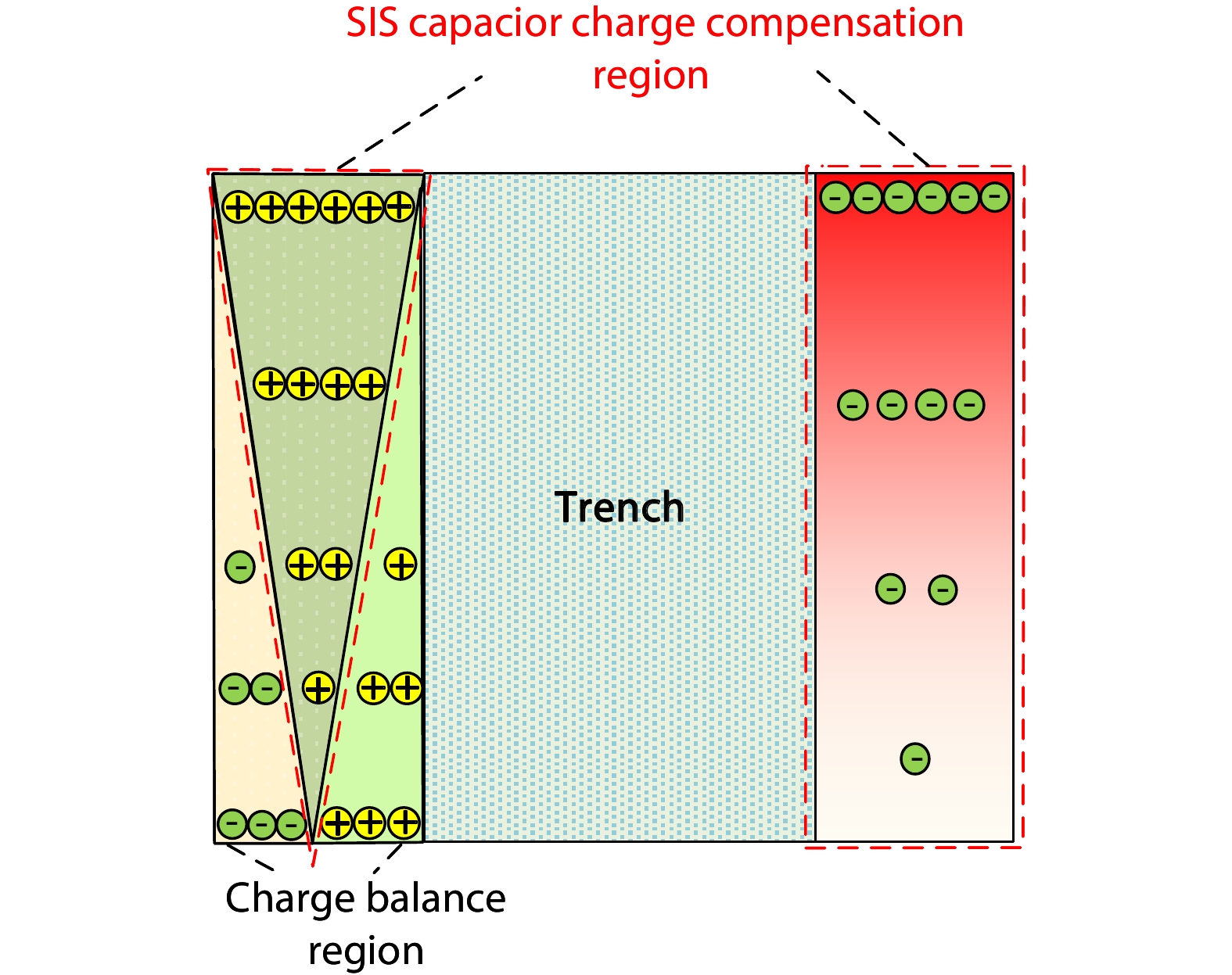
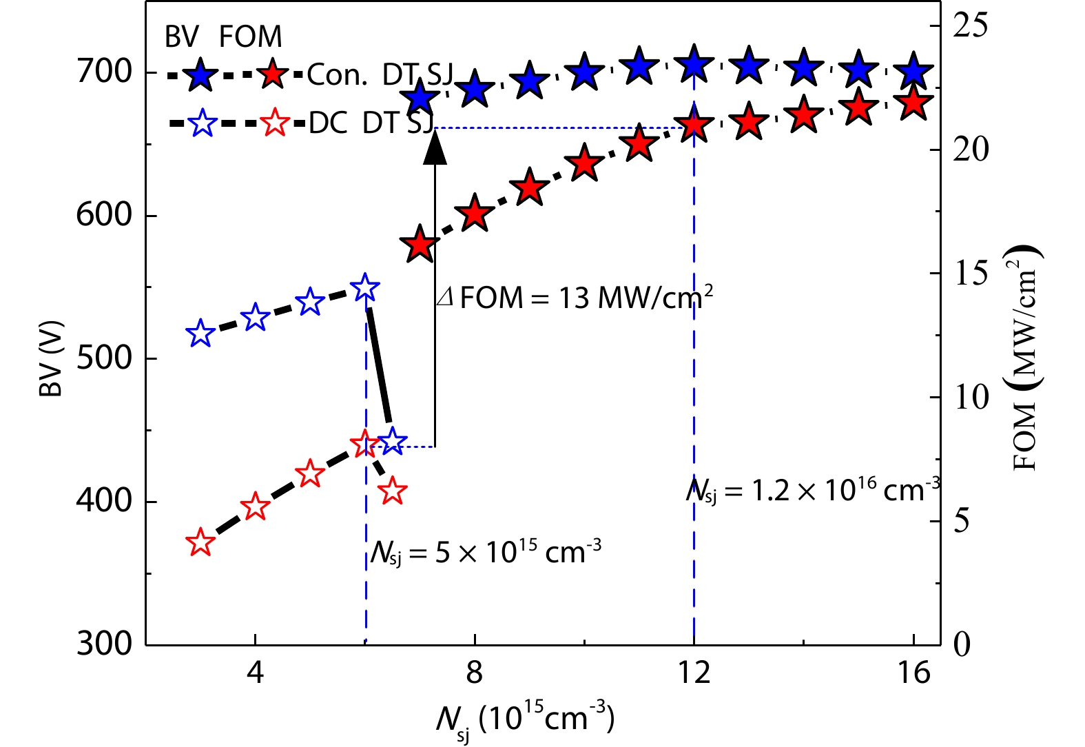
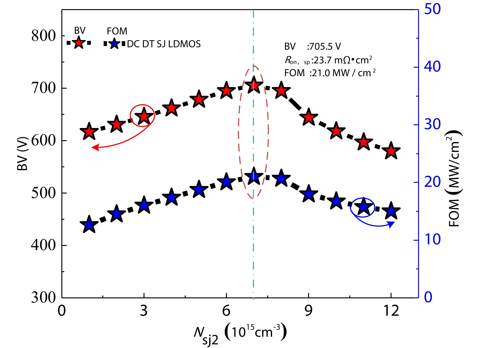
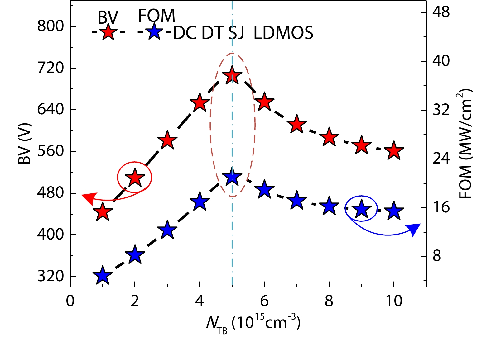
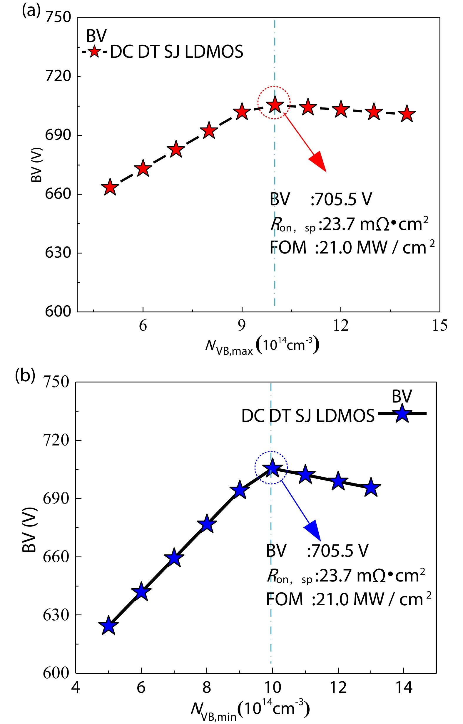
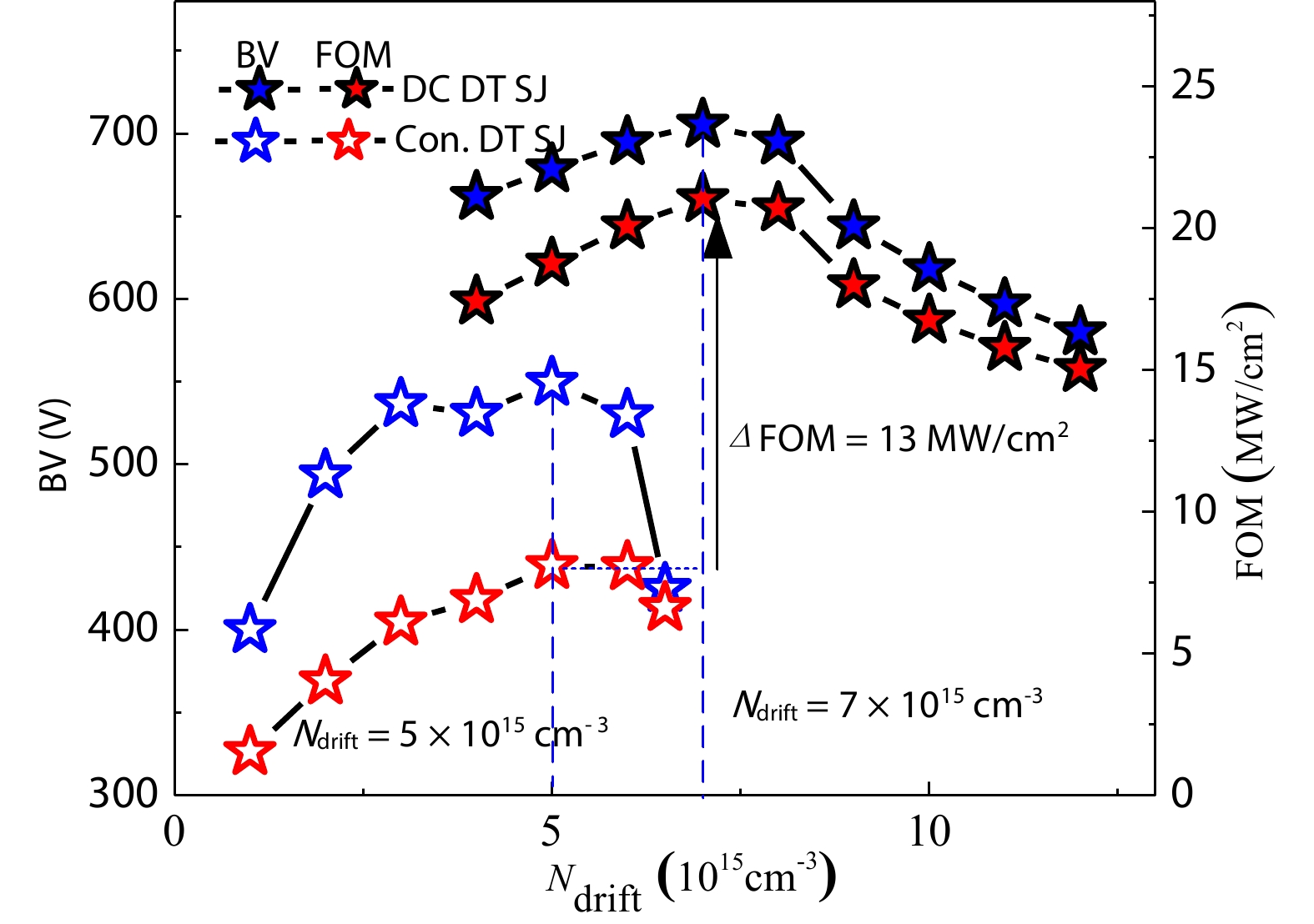
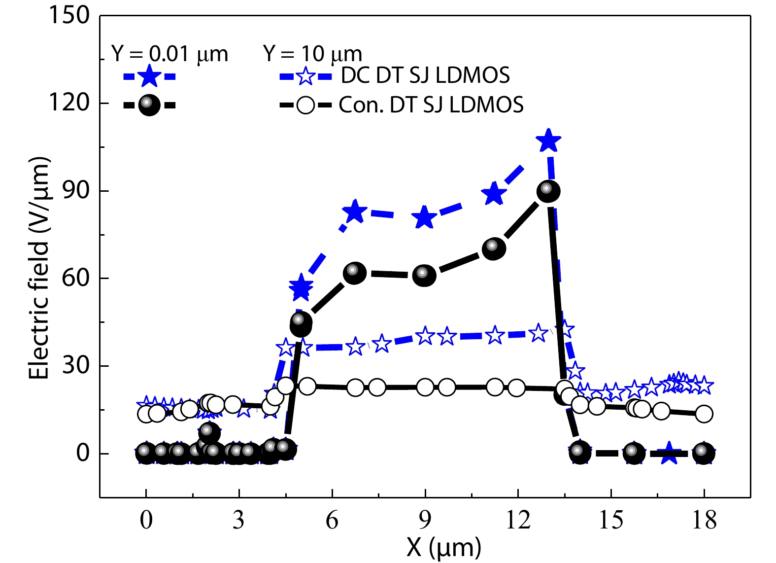
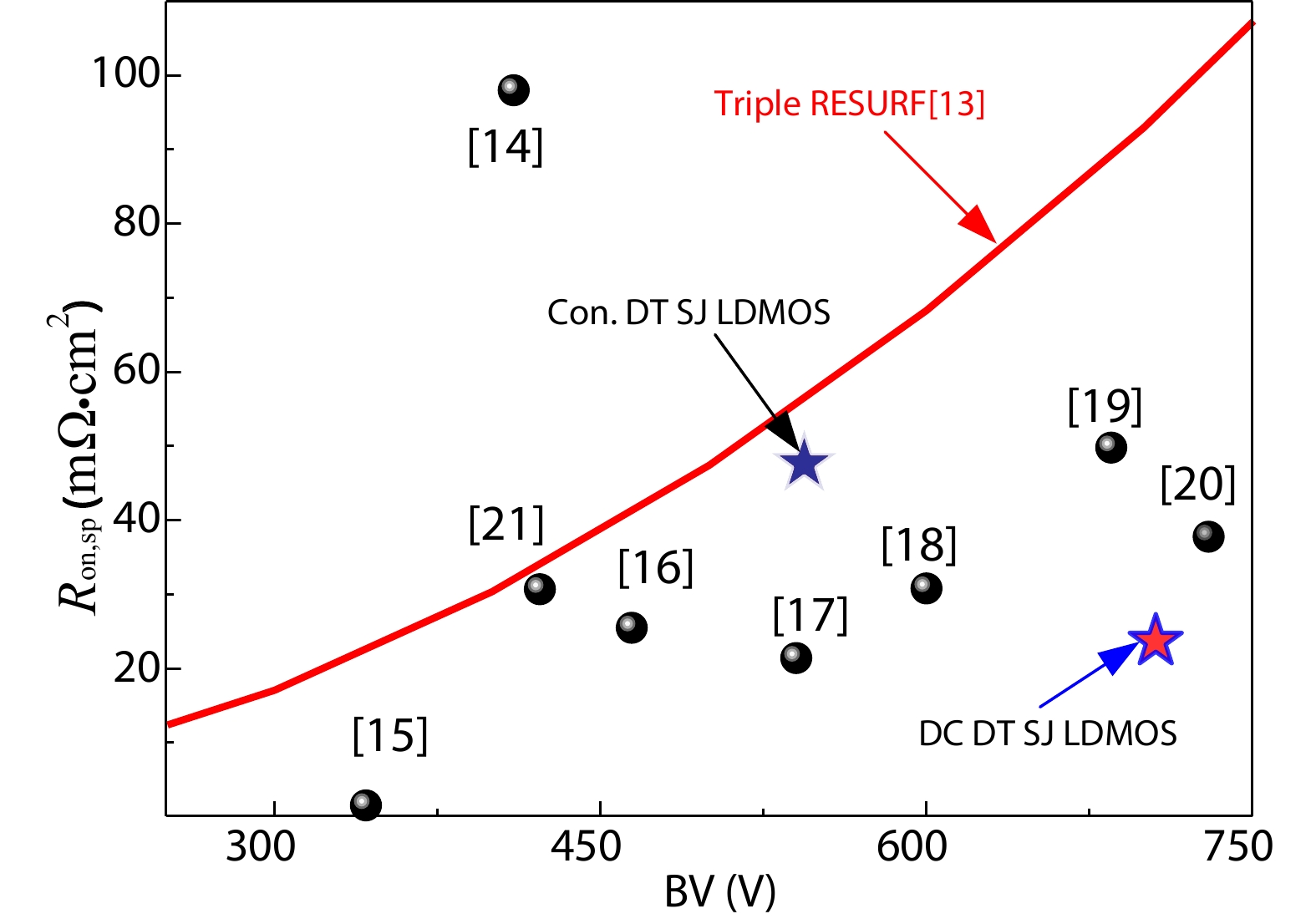
A deep trench super-junction LDMOS with double charge compensation layer (DC DT SJ LDMOS) is proposed in this paper. Due to the capacitance effect of the deep trench which is known as silicon–insulator–silicon (SIS) capacitance, the charge balance in the super-junction region of the conventional deep trench SJ LDMOS (Con. DT SJ LDMOS) device will be broken, resulting in breakdown voltage (BV) of the device drops. DC DT SJ LDMOS solves the SIS capacitance effect by adding a vertical variable doped charge compensation layer and a triangular charge compensation layer inside the Con. DT SJ LDMOS device. Therefore, the drift region reaches an ideal charge balance state again. The electric field is optimized by double charge compensation and gate field plate so that the breakdown voltage of the proposed device is improved sharply, meanwhile the enlarged on-current region reduces its specific on-resistance. The simulation results show that compared with the Con. DT SJ LDMOS, the BV of the DC DT SJ LDMOS has been increased from 549.5 to 705.5 V, and the Ron,sp decreased to 23.7 mΩ·cm2.


J. Semicond.
2022, 43(10): 102001 doi: 10.1088/1674-4926/43/10/102001
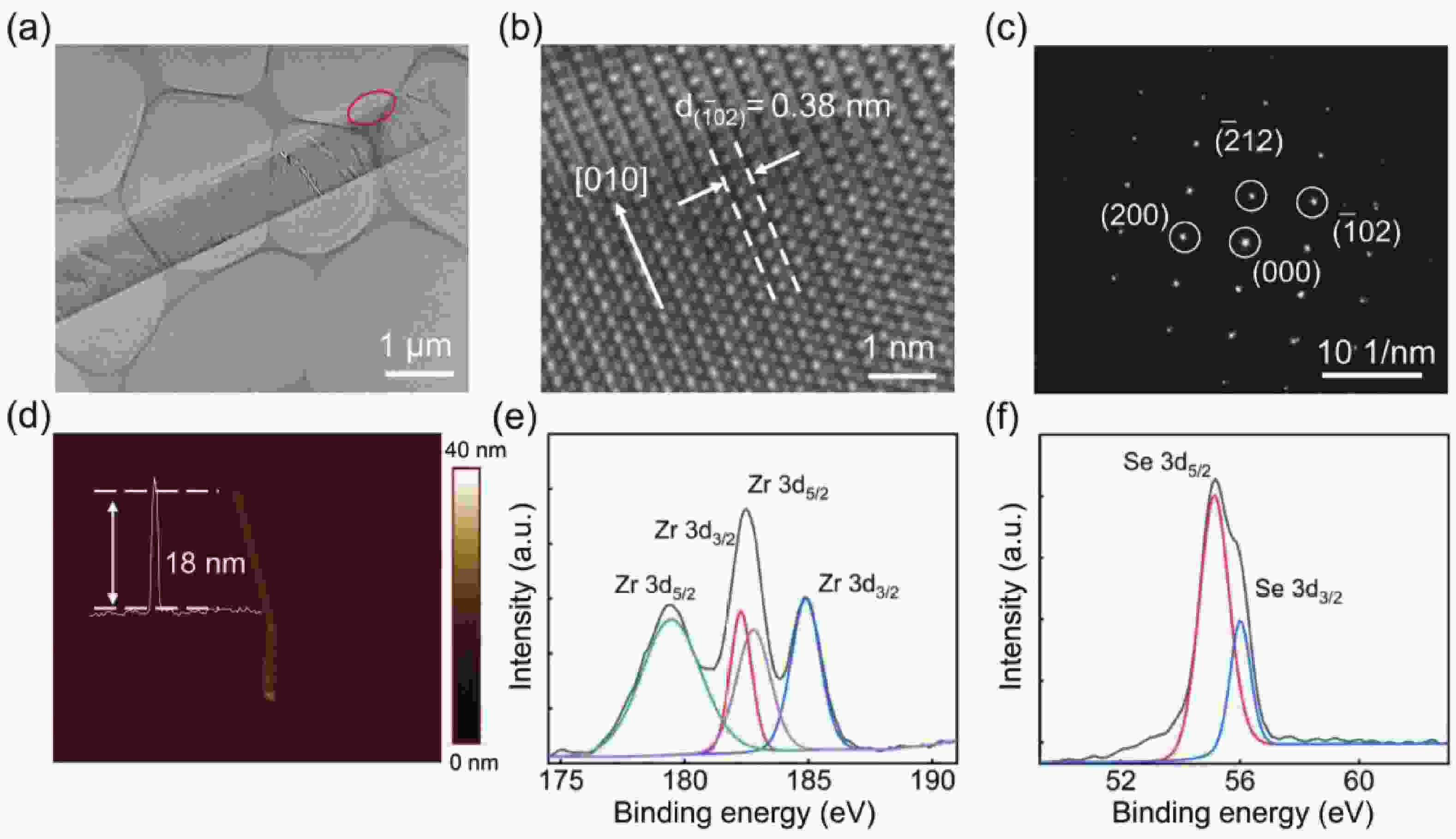
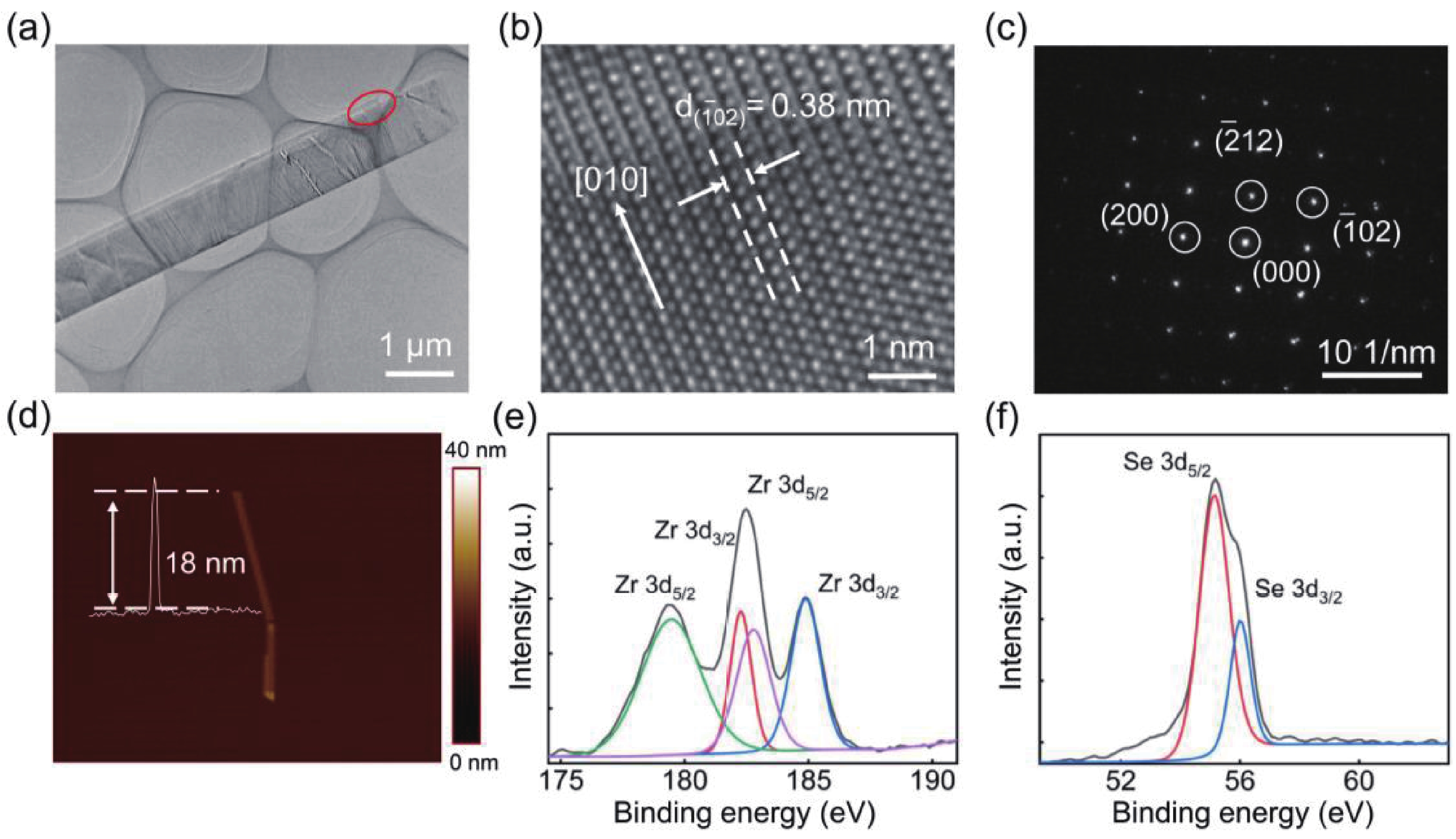
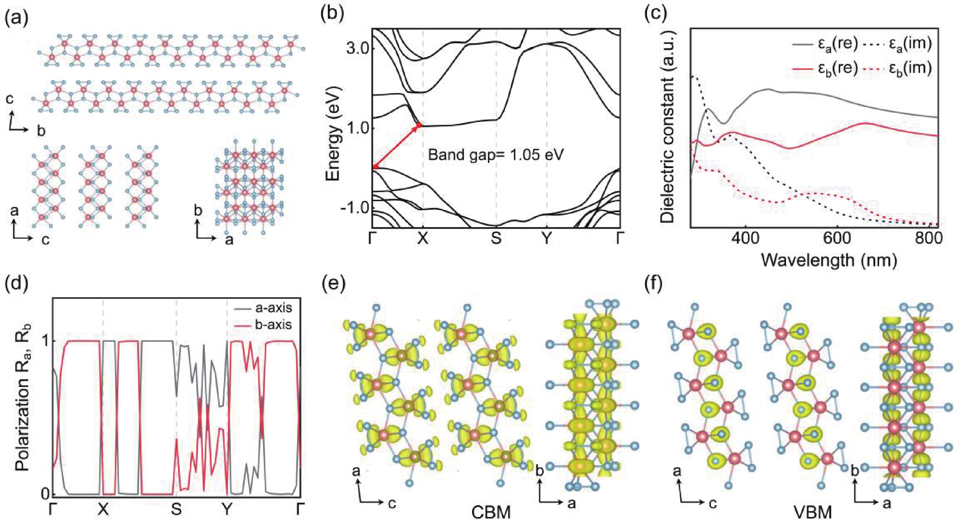
The in-plane anisotropy of transition metal trichalcogenides (MX3) has a significant impact on the molding of materials and MX3 is a perfect choice for polarized photodetectors. In this study, the crystal structure, optical and optoelectronic anisotropy of one kind of quasi-one-dimensional (1D) semiconductors, ZrSe3, are systematically investigated through experiments and theoretical studies. The ZrSe3-based photodetector shows impressive wide spectral response from ultraviolet (UV) to near infrared (NIR) and exhibits great optoelectrical properties with photoresponsivity of 11.9 mA·W-1 and detectivity of ~106 at 532 nm. Moreover, the dichroic ratio of ZrSe3-based polarized photodetector is around 1.1 at 808 nm. This study suggests that ZrSe3 has potential in optoelectronic applications and polarization detectors.