ARTICLES

Ni/Pd-based ohmic contacts to p-GaN through p-InGaN/p+-GaN contacting layers

Minglong Zhang1, 2, Masao Ikeda1, 2, , Siyi Huang1, 2, Jianping Liu1, 2, , Jianjun Zhu2, Shuming Zhang1, 2 and Hui Yang1, 2

+ Author Affiliations

 Corresponding author: Masao Ikeda, mikeda2013@sinano.ac.cn; Jianping Liu, jpliu2010@sinano.ac.cn

PDF

Turn off MathJax

Abstract: Specific contact resistance $ {\rho }_{\mathrm{c}} $ to p-GaN was measured for various structures of Ni/Pd-based metals and thin (20–30 nm thick) p-InGaN/p+-GaN contacting layers. The effects of surface chemical treatment and annealing temperature were examined. The optimal annealing temperature was determined to be 550 °C, above which the sheet resistance of the samples degraded considerably, suggesting that undesirable alloying had occurred. Pd-containing metal showed ~35% lower $ {\rho }_{\mathrm{c}} $ compared to that of single Ni. Very thin (2–3.5 nm thick) p-InGaN contacting layers grown on 20–25 nm thick p+-GaN layers exhibited one to two orders of magnitude smaller values of $ {\rho }_{\mathrm{c}} $ compared to that of p+-GaN without p-InGaN. The current density dependence of $ {\rho }_{\mathrm{c}} $, which is indicative of nonlinearity in current-voltage relation, was also examined. The lowest $ {\rho }_{\mathrm{c}} $ achieved through this study was 4.9 × 10⁻⁵ Ω·cm2 @ J = 3.4 kA/cm2.

Key words: GaNohmic contactspecific contact resistance


[1]
Nakamura S. The roles of structural imperfections in InGaN-based blue light-emitting diodes and laser diodes. Science, 1998, 281, 956 doi: 10.1126/science.281.5379.956
[2]
Hu L, Ren X Y, Liu J P, et al. High-power hybrid GaN-based green laser diodes with ITO cladding layer. Photonics Res, 2020, 8, 279 doi: 10.1364/PRJ.381262
[3]
Li L, Nomoto K, Pan M, et al. GaN HEMTs on Si with regrown contacts and cutoff/maximum oscillation frequencies of 250/204 GHz. IEEE Electron Device Lett, 2020, 41, 689 doi: 10.1109/LED.2020.2984727
[4]
Koide Y, Maeda T, Kawakami T, et al. Effects of annealing in an oxygen ambient on electrical properties of ohmic contacts to p-type GaN. J Electron Mater, 1999, 28, 341 doi: 10.1007/s11664-999-0037-7
[5]
Luther B P, Mohney S E, Jackson T N, et al. Investigation of the mechanism for Ohmic contact formation in Al and Ti/Al contacts to n-type GaN. Appl Phys Lett, 1997, 70, 57 doi: 10.1063/1.119305
[6]
Singh K, Chauhan A, Mathew M, et al. Formation of non-alloyed Ti/Al/Ni/Au low-resistance ohmic contacts on reactively ion-etched n-type GaN by surface treatment for GaN light-emitting diodes applications. Appl Phys A, 2019, 125, 24 doi: 10.1007/s00339-018-2322-x
[7]
Tanaka T, Watanabe A, Amano H, et al. P-type conduction in Mg-doped GaN and Al0.08Ga0.92N grown by metalorganic vapor phase epitaxy. Appl Phys Lett, 1994, 65, 593 doi: 10.1063/1.112309
[8]
Ho J K, Jong C S, Chiu C C, et al. Low-resistance ohmic contacts to p-type GaN. Appl Phys Lett, 1999, 74, 1275 doi: 10.1063/1.123546
[9]
Kim J K, Lee J L, Lee J W, et al. Low resistance Pd/Au ohmic contacts to p-type GaN using surface treatment. Appl Phys Lett, 1998, 73, 2953 doi: 10.1063/1.122641
[10]
Wahid S, Chowdhury N, Alam M K, et al. Barrier heights and Fermi level pinning in metal contacts on p-type GaN. Appl Phys Lett, 2020, 116, 213506 doi: 10.1063/5.0010699
[11]
Wang W J, Xie W Z, Deng Z J, et al. Performance improvement of GaN based laser diode using Pd/Ni/Au metallization ohmic contact. Coatings, 2019, 9, 291 doi: 10.3390/coatings9050291
[12]
Chary I, Chandolu A, Borisov B, et al. Influence of surface treatment and annealing temperature. J Electron Mater, 2009, 38, 545 doi: 10.1007/s11664-008-0655-5
[13]
Mallem S P R, Ahn W H, Lee J H, et al. Influence of thermal annealing on the PdAl/Au metal stack ohmic contacts to p-AlGaN. Crystals, 2020, 10, 1091 doi: 10.3390/cryst10121091
[14]
Lee J L, Weber M, Kim J K, et al. Ohmic contact formation mechanism of nonalloyed Pd contacts to p-type GaN observed by positron annihilation spectroscopy. Appl Phys Lett, 1999, 74, 2289 doi: 10.1063/1.123827
[15]
Song J O, Leem D S, Kwak J S, et al. High-quality nonalloyed rhodium-based ohmic contacts to p-type GaN. Appl Phys Lett, 2003, 83, 2372 doi: 10.1063/1.1613991
[16]
He J L, Zhong Y Z, Zhou Y, et al. Recovery of p-GaN surface damage induced by dry etching for the formation of p-type Ohmic contact. Appl Phys Express, 2019, 12, 055507 doi: 10.7567/1882-0786/ab13d7
[17]
Kumakura K, Makimoto T, Kobayashi N. Ohmic contact to p-GaN using a strained InGaN contact layer and its thermal stability. Jpn J Appl Phys, 2003, 42, 2254 doi: 10.1143/JJAP.42.2254
[18]
Trexler J T, Pearton S J, Holloway P H, et al. Comparison of Ni/Au, Pd/Au, and Cr/Au metallizations for ohmic contacts to p-GaN. MRS Online Proc Libr, 1996, 449, 1091 doi: 10.1557/PROC-449-1091
[19]
Bernardini F, Fiorentini V. Spontaneous versus piezoelectric polarization in III-V nitrides: Conceptual aspects and practical consequences. Phys Status Solidi B, 1999, 216, 391 doi: 10.1002/(SICI)1521-3951(199911)216:1<391::AID-PSSB391>3.0.CO;2-K
[20]
Weimar A, Lell A, Brüderl G, et al. Investigation of low-resistance metal contacts on p-type GaN using the linear and circular transmission line method. Phys Status Solidi A, 2001, 183, 169 doi: 10.1002/1521-396X(200101)183:1<169::AID-PSSA169>3.0.CO;2-D
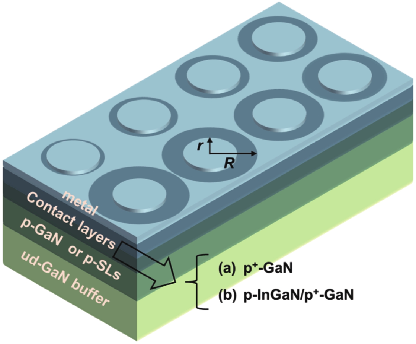
Fig. 1.  (Color online) Schematic illustration of the contact layer structure and c-TLM pattern used to measure contact resistance.

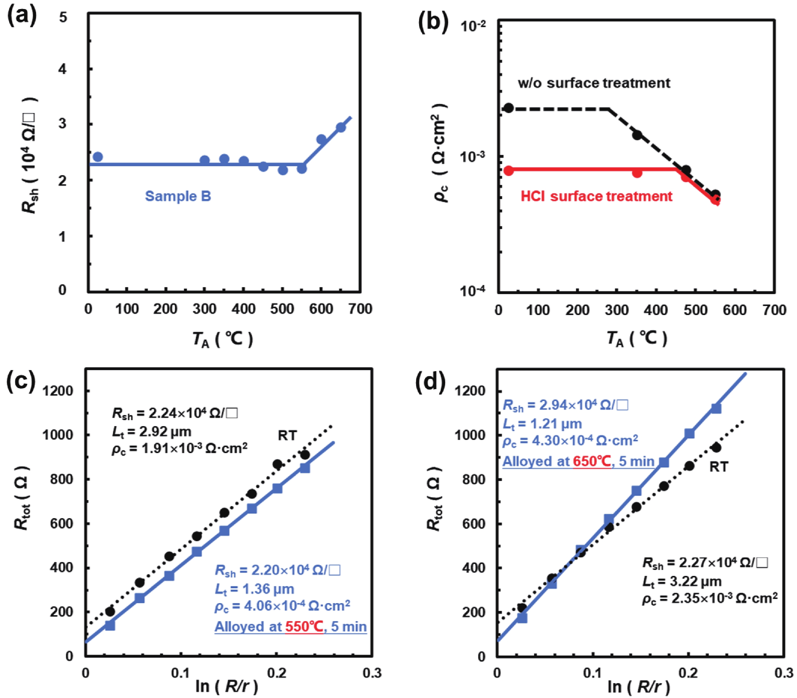
Fig. 2.  (Color online) (a) The measured values of sheet resistance after annealing at various temperatures. (b) Comparison of the annealing temperature dependence of $ {\rho }_{\mathrm{c}} $ between with and without the chemical surface treatment. (c, d) c-TLM-data examples for annealing temperature of 550 and 650 °C, respectively.

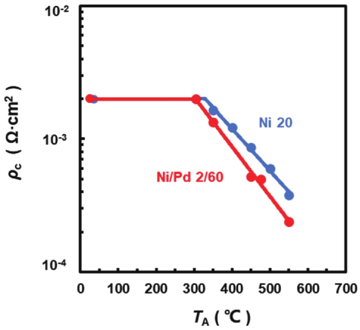
Fig. 3.  (Color online) Comparison of TA-dependence of ${\rho }_{\rm c}$ between Ni 20 and Ni/Pd 2/60 contacts.

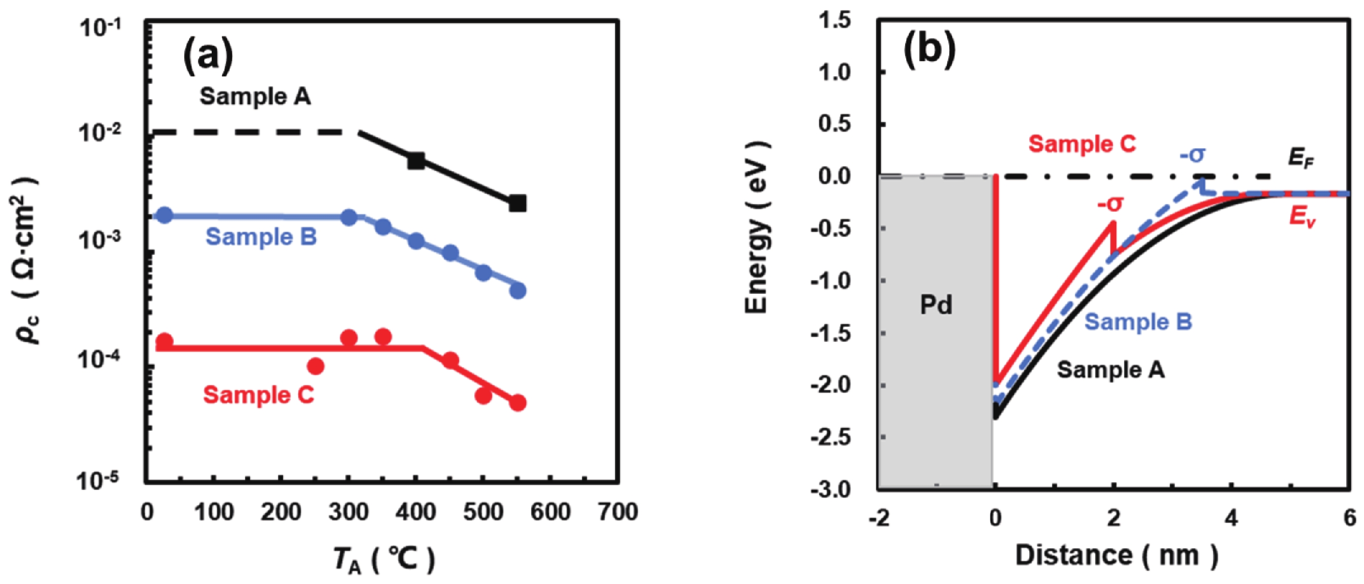
Fig. 4.  (Color online) (a) Comparison of $ {\rho }_{\mathrm{c}} $TA relation among three samples listed in Table 1. (b) Simulated valence band curves near the contact depletion region for the three samples.

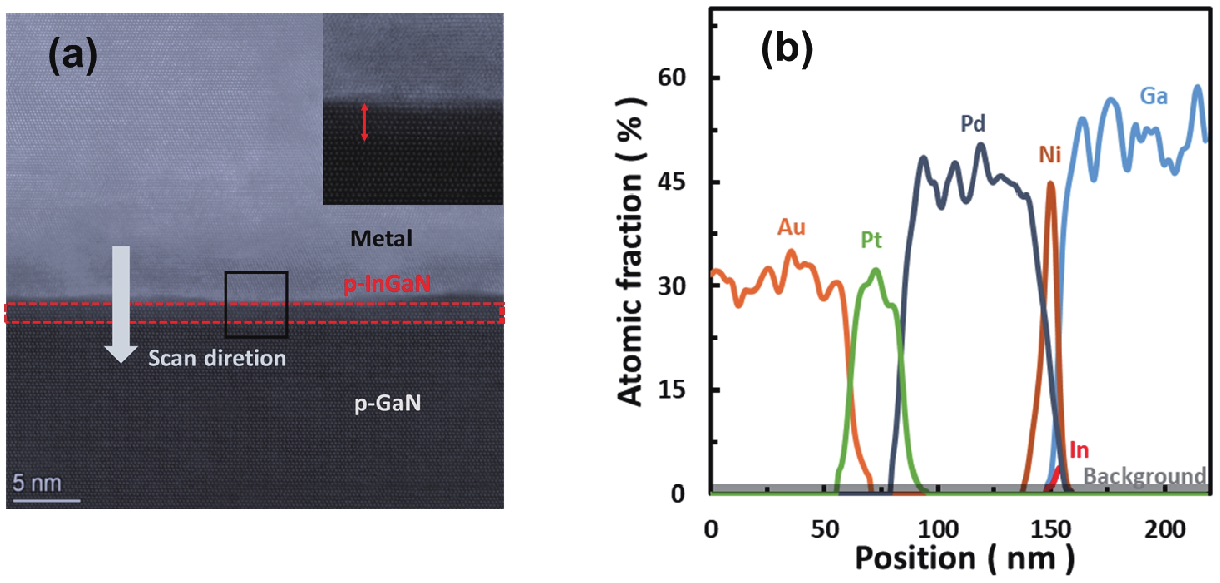
Fig. 5.  (Color online) (a) STEM cross-sectional image of the sample C annealed at 550 °C. (b) EDX line analysis of Ga, In, Ni, Pd, Pt, and Au recorded along the blue arrow in Fig. 5(a).

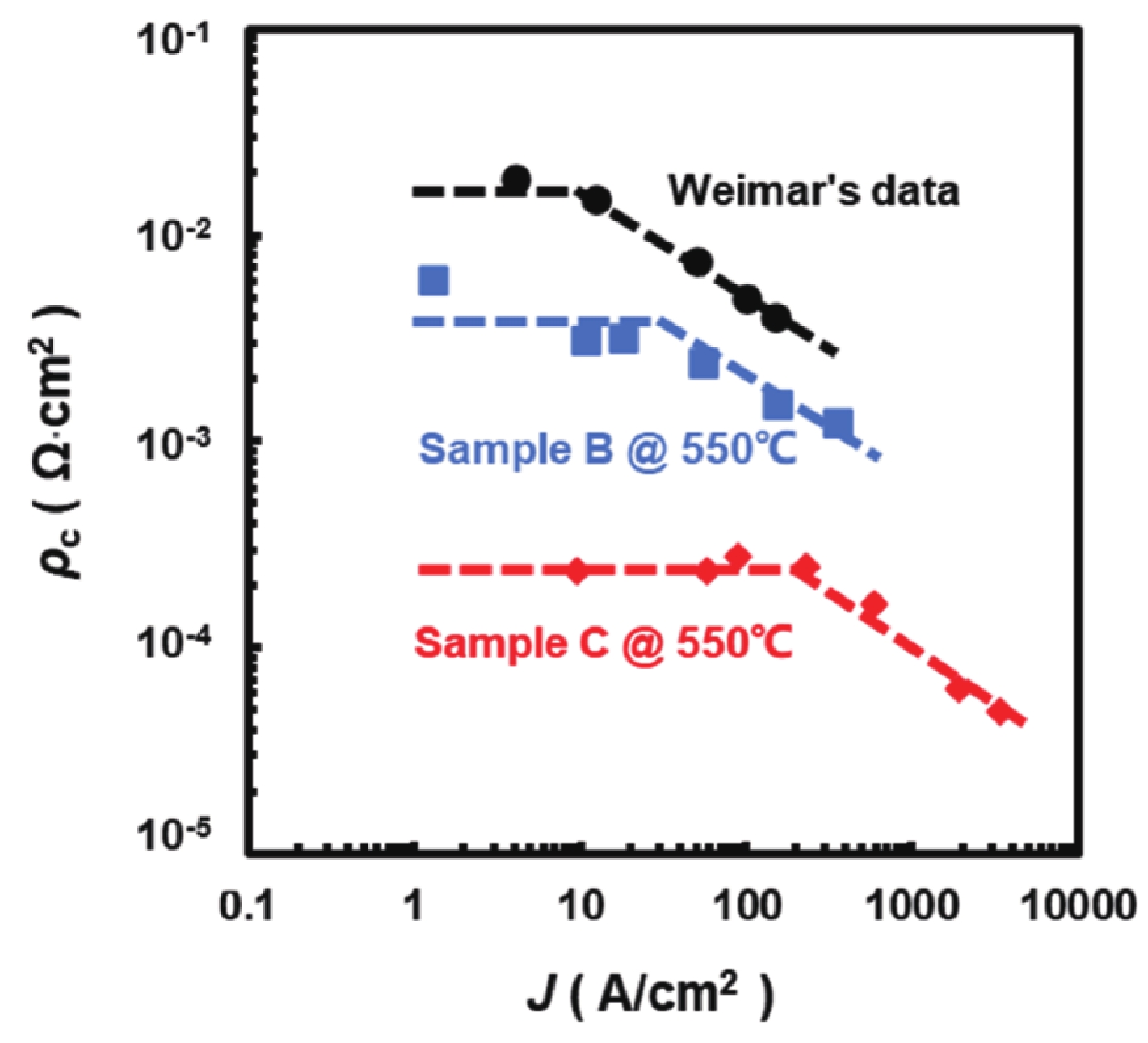
Fig. 6.  (Color online) The specific contact resistance $ {\rho }_{\mathrm{c}} $ as a function of current density.

Table 1.   Details of the structures of Ni/Pd-based metals and p-InGaN/p+-GaN contacting layers.

Sample
dp+-GaN (nm)[Mg]p+-GaN (1020 cm–3)dp-InGaN (nm)[Mg]p-InGaN (1019 cm–3)Xp-InGaN (%)Metal scheme
Surface treatment
A251Ni 20w/o
B2013.587Ni 20w/o
C2212420Ni/Pd 2/60w
DownLoad: CSV
[1]
Nakamura S. The roles of structural imperfections in InGaN-based blue light-emitting diodes and laser diodes. Science, 1998, 281, 956 doi: 10.1126/science.281.5379.956
[2]
Hu L, Ren X Y, Liu J P, et al. High-power hybrid GaN-based green laser diodes with ITO cladding layer. Photonics Res, 2020, 8, 279 doi: 10.1364/PRJ.381262
[3]
Li L, Nomoto K, Pan M, et al. GaN HEMTs on Si with regrown contacts and cutoff/maximum oscillation frequencies of 250/204 GHz. IEEE Electron Device Lett, 2020, 41, 689 doi: 10.1109/LED.2020.2984727
[4]
Koide Y, Maeda T, Kawakami T, et al. Effects of annealing in an oxygen ambient on electrical properties of ohmic contacts to p-type GaN. J Electron Mater, 1999, 28, 341 doi: 10.1007/s11664-999-0037-7
[5]
Luther B P, Mohney S E, Jackson T N, et al. Investigation of the mechanism for Ohmic contact formation in Al and Ti/Al contacts to n-type GaN. Appl Phys Lett, 1997, 70, 57 doi: 10.1063/1.119305
[6]
Singh K, Chauhan A, Mathew M, et al. Formation of non-alloyed Ti/Al/Ni/Au low-resistance ohmic contacts on reactively ion-etched n-type GaN by surface treatment for GaN light-emitting diodes applications. Appl Phys A, 2019, 125, 24 doi: 10.1007/s00339-018-2322-x
[7]
Tanaka T, Watanabe A, Amano H, et al. P-type conduction in Mg-doped GaN and Al0.08Ga0.92N grown by metalorganic vapor phase epitaxy. Appl Phys Lett, 1994, 65, 593 doi: 10.1063/1.112309
[8]
Ho J K, Jong C S, Chiu C C, et al. Low-resistance ohmic contacts to p-type GaN. Appl Phys Lett, 1999, 74, 1275 doi: 10.1063/1.123546
[9]
Kim J K, Lee J L, Lee J W, et al. Low resistance Pd/Au ohmic contacts to p-type GaN using surface treatment. Appl Phys Lett, 1998, 73, 2953 doi: 10.1063/1.122641
[10]
Wahid S, Chowdhury N, Alam M K, et al. Barrier heights and Fermi level pinning in metal contacts on p-type GaN. Appl Phys Lett, 2020, 116, 213506 doi: 10.1063/5.0010699
[11]
Wang W J, Xie W Z, Deng Z J, et al. Performance improvement of GaN based laser diode using Pd/Ni/Au metallization ohmic contact. Coatings, 2019, 9, 291 doi: 10.3390/coatings9050291
[12]
Chary I, Chandolu A, Borisov B, et al. Influence of surface treatment and annealing temperature. J Electron Mater, 2009, 38, 545 doi: 10.1007/s11664-008-0655-5
[13]
Mallem S P R, Ahn W H, Lee J H, et al. Influence of thermal annealing on the PdAl/Au metal stack ohmic contacts to p-AlGaN. Crystals, 2020, 10, 1091 doi: 10.3390/cryst10121091
[14]
Lee J L, Weber M, Kim J K, et al. Ohmic contact formation mechanism of nonalloyed Pd contacts to p-type GaN observed by positron annihilation spectroscopy. Appl Phys Lett, 1999, 74, 2289 doi: 10.1063/1.123827
[15]
Song J O, Leem D S, Kwak J S, et al. High-quality nonalloyed rhodium-based ohmic contacts to p-type GaN. Appl Phys Lett, 2003, 83, 2372 doi: 10.1063/1.1613991
[16]
He J L, Zhong Y Z, Zhou Y, et al. Recovery of p-GaN surface damage induced by dry etching for the formation of p-type Ohmic contact. Appl Phys Express, 2019, 12, 055507 doi: 10.7567/1882-0786/ab13d7
[17]
Kumakura K, Makimoto T, Kobayashi N. Ohmic contact to p-GaN using a strained InGaN contact layer and its thermal stability. Jpn J Appl Phys, 2003, 42, 2254 doi: 10.1143/JJAP.42.2254
[18]
Trexler J T, Pearton S J, Holloway P H, et al. Comparison of Ni/Au, Pd/Au, and Cr/Au metallizations for ohmic contacts to p-GaN. MRS Online Proc Libr, 1996, 449, 1091 doi: 10.1557/PROC-449-1091
[19]
Bernardini F, Fiorentini V. Spontaneous versus piezoelectric polarization in III-V nitrides: Conceptual aspects and practical consequences. Phys Status Solidi B, 1999, 216, 391 doi: 10.1002/(SICI)1521-3951(199911)216:1<391::AID-PSSB391>3.0.CO;2-K
[20]
Weimar A, Lell A, Brüderl G, et al. Investigation of low-resistance metal contacts on p-type GaN using the linear and circular transmission line method. Phys Status Solidi A, 2001, 183, 169 doi: 10.1002/1521-396X(200101)183:1<169::AID-PSSA169>3.0.CO;2-D
  • Search

    Advanced Search >>

    GET CITATION

    shu

    Export: BibTex EndNote

    Article Metrics

    Article views: 985 Times PDF downloads: 127 Times Cited by: 0 Times

    History

    Received: 29 March 2022 Revised: 08 May 2022 Online: Accepted Manuscript: 26 June 2022Uncorrected proof: 27 June 2022Published: 02 September 2022

    Catalog

      Email This Article

      User name:
      Email:*请输入正确邮箱
      Code:*验证码错误
      Minglong Zhang, Masao Ikeda, Siyi Huang, Jianping Liu, Jianjun Zhu, Shuming Zhang, Hui Yang. Ni/Pd-based ohmic contacts to p-GaN through p-InGaN/p+-GaN contacting layers[J]. Journal of Semiconductors, 2022, 43(9): 092803. doi: 10.1088/1674-4926/43/9/092803 M L Zhang, M Ikeda, S Y Huang, J P Liu, J J Zhu, S M Zhang, H Yang. Ni/Pd-based ohmic contacts to p-GaN through p-InGaN/p+-GaN contacting layers[J]. J. Semicond, 2022, 43(9): 092803. doi: 10.1088/1674-4926/43/9/092803Export: BibTex EndNote
      Citation:
      Minglong Zhang, Masao Ikeda, Siyi Huang, Jianping Liu, Jianjun Zhu, Shuming Zhang, Hui Yang. Ni/Pd-based ohmic contacts to p-GaN through p-InGaN/p+-GaN contacting layers[J]. Journal of Semiconductors, 2022, 43(9): 092803. doi: 10.1088/1674-4926/43/9/092803

      M L Zhang, M Ikeda, S Y Huang, J P Liu, J J Zhu, S M Zhang, H Yang. Ni/Pd-based ohmic contacts to p-GaN through p-InGaN/p+-GaN contacting layers[J]. J. Semicond, 2022, 43(9): 092803. doi: 10.1088/1674-4926/43/9/092803
      Export: BibTex EndNote

      Ni/Pd-based ohmic contacts to p-GaN through p-InGaN/p+-GaN contacting layers

      doi: 10.1088/1674-4926/43/9/092803
      More Information
      • Author Bio:

        Minglong Zhang is a Master’s student at the School of Nano-Tech and Nano-Bionics, University ofScience and Technology of China, under the supervision of Prof. Masao Ikeda and Prof. Jianping Liu. His research focuses on the fabrication process of GaN-based lasers

        Masao Ikeda received the Ph.D. degree from Waseda University, Tokyo, Japan, in 1991. He is currently a Professor with the Suzhou Institute of Nano-Tech and Nano-Bionics, Chinese Academy of Sciences, Suzhou, China. His current research interests include III–V compound semiconductor materials and devices

        Jianping Liu is a professor in Suzhou Institute of Nano-Tech and Nano-Bionics, Chinese Academy of Sciences. He earned his doctoral degree from Institute of Semiconductors, Chinese Academy of Sciences in 2004. He worked at Lab of Optoelectronics Technology at Beijing University of Technology from 2004 to 2006. He did postdoctoral research in Department of Electrical Engineering at Georgia Institute of Technology from 2006 to 2010. His research interests include MOCVD growth, GaN-based materials and devices

      • Corresponding author: mikeda2013@sinano.ac.cnjpliu2010@sinano.ac.cn
      • Received Date: 2022-03-29
      • Revised Date: 2022-05-08
      • Available Online: 2022-06-26

      Catalog

        /

        DownLoad:  Full-Size Img  PowerPoint
        Return
        Return