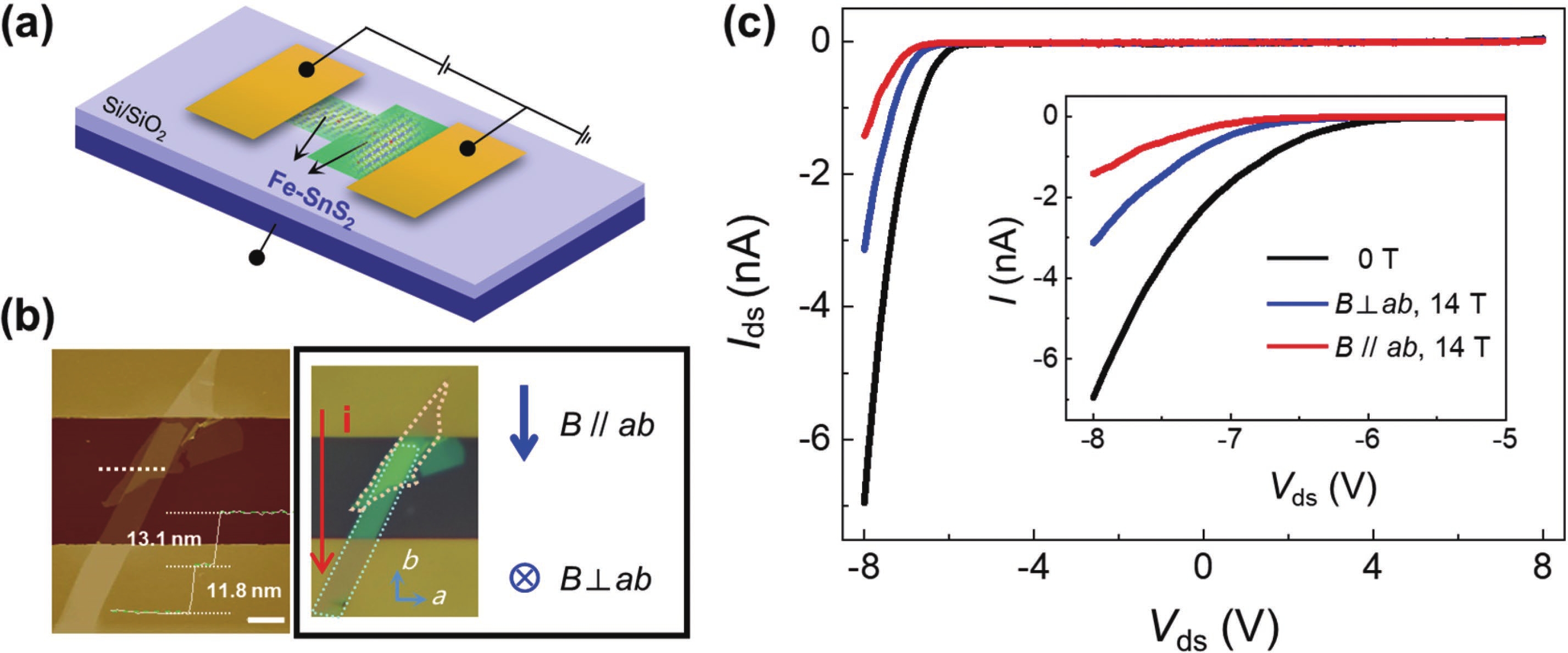
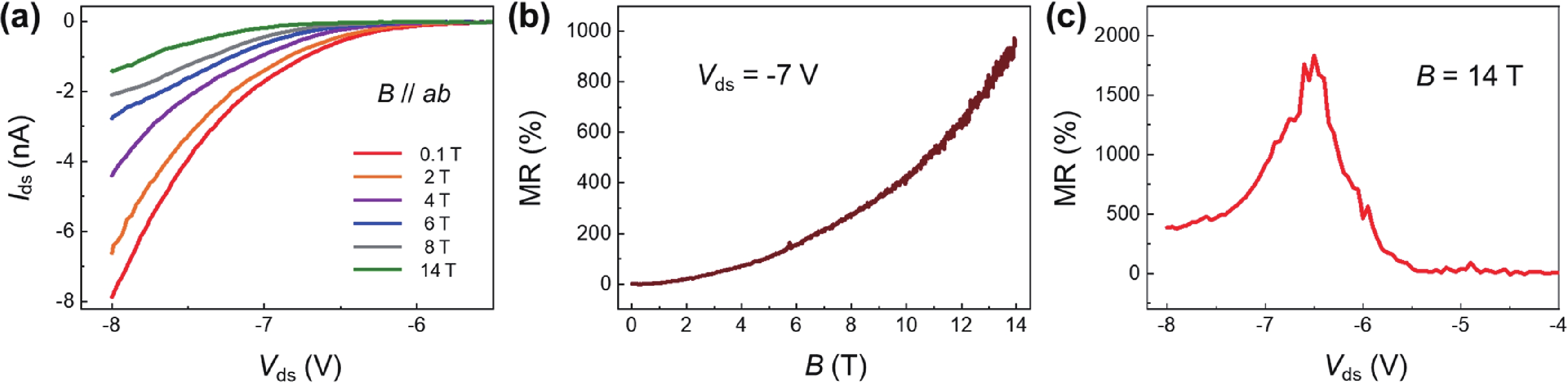
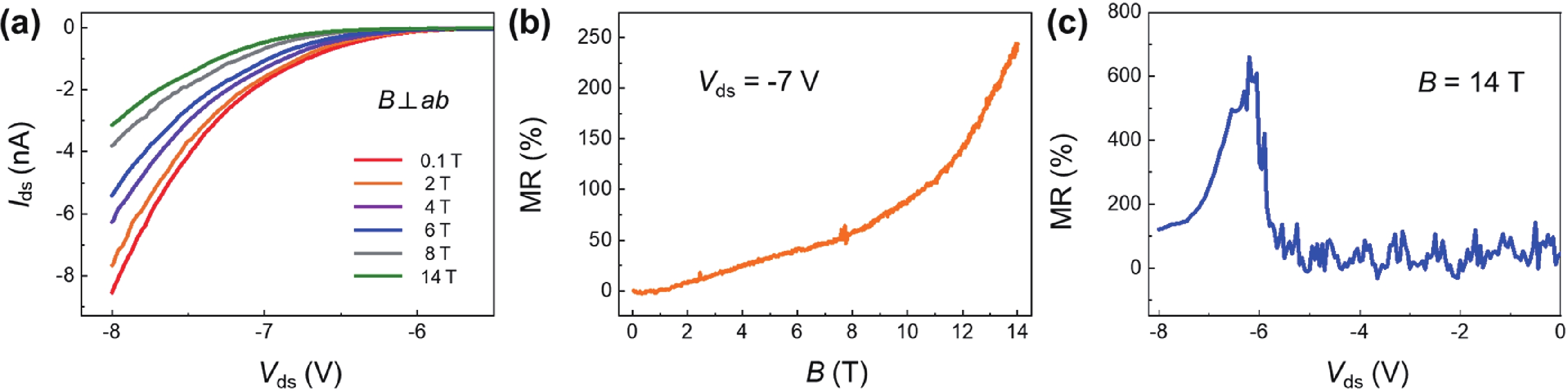
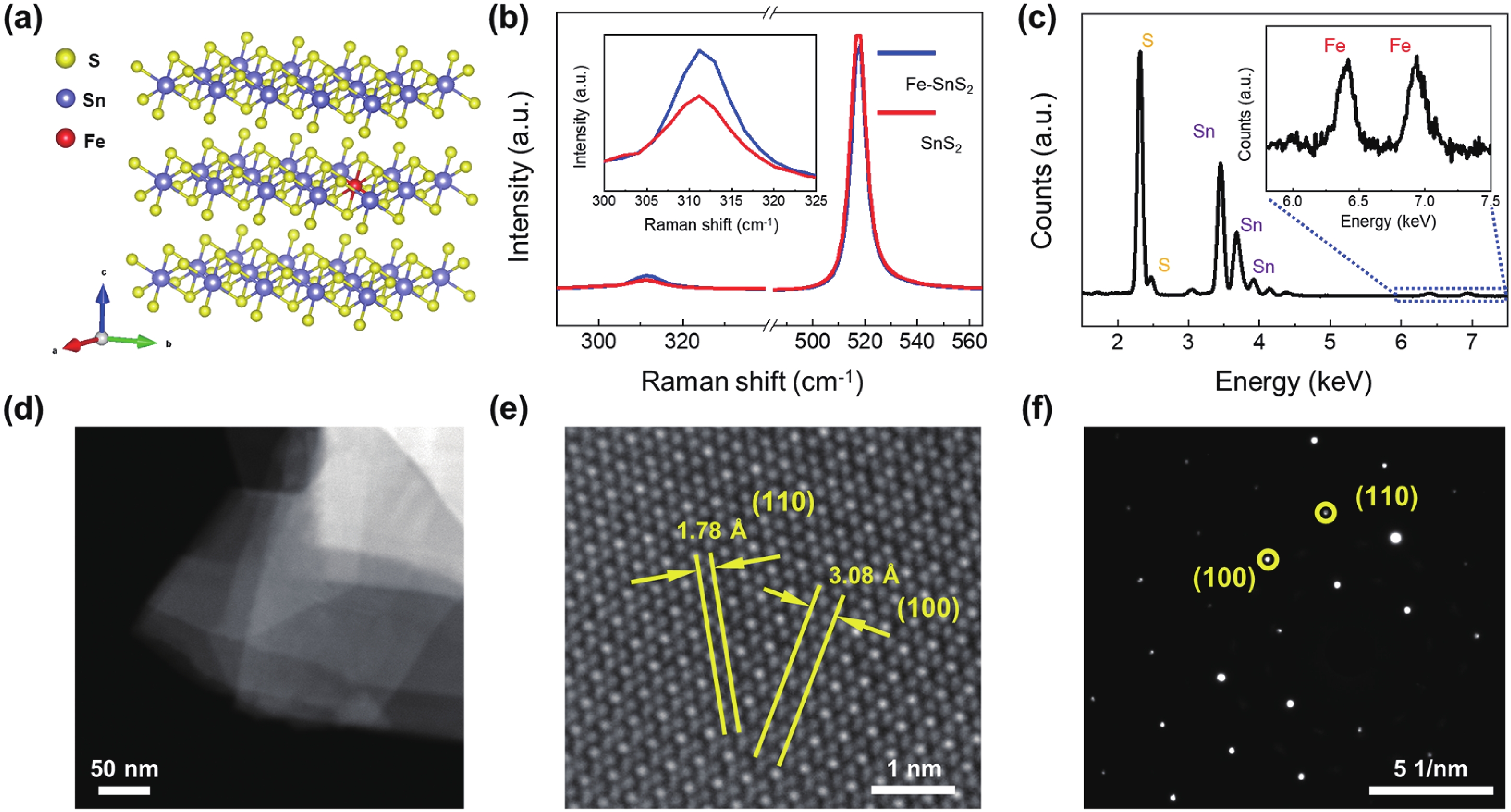
ARTICLES

Large unsaturated magnetoresistance of 2D magnetic semiconductor Fe-SnS2 homojunction

Jingzhi Fang1, 2, 3, 4, Huading Song3, Bo Li5, Ziqi Zhou1, 2, 3, Juehan Yang1, 2, Benchuan Lin4, Zhimin Liao3, and Zhongming Wei1, 2,

+ Author Affiliations

 Corresponding author: Zhimin Liao, liaozm@pku.edu.cn; Zhongming Wei, zmwei@semi.ac.cn

PDF

Turn off MathJax

Abstract: A magnetic semiconductor whose electronic charge and spin can be regulated together will be an important component of future spintronic devices. Here, we construct a two-dimensional (2D) Fe doped SnS2 (Fe-SnS2) homogeneous junction and investigate its electromagnetic transport feature. The Fe-SnS2 homojunction device showed large positive and unsaturated magnetoresistance (MR) of 1800% in the parallel magnetic field and 600% in the vertical magnetic field, indicating an obvious anisotropic MR feature. In contrast, The MR of Fe-SnS2 homojunction is much larger than the pure diamagnetic SnS2 and most 2D materials. The application of a gate voltage can regulate the MR effect of Fe-SnS2 homojunction devices. Moreover, the stability of Fe-SnS2 in air has great application potential. Our Fe-SnS2 homojunction has a significant potential in future magnetic memory applications.

Key words: magnetic semiconductorhomojunctionmagnetoresistanceMR anisotropic


[1]
Gong C, Zhang X. Two-dimensional magnetic crystals and emergent heterostructure devices. Science, 2019, 363, 706 doi: 10.1126/science.aav4450
[2]
Song T, Cai X, Tu M W, et al. Giant tunneling magnetoresistance in spin-filter van der Waals heterostructures. Science, 2018, 360, 1214 doi: 10.1126/science.aar4851
[3]
Bhatti S, Sbiaa R, Hirohata A, et al. Spintronics based random access memory: a review. Mater Today, 2017, 20, 530 doi: 10.1016/j.mattod.2017.07.007
[4]
Wang Z, Gutierrez-Lezama I, Ubrig N, et al. Very large tunneling magnetoresistance in layered magnetic semiconductor CrI3. Nat Commun, 2018, 9, 2516 doi: 10.1038/s41467-018-04953-8
[5]
Ikeda S, Hayakawa J, Ashizawa Y, et al. Tunnel magnetoresistance of 604% at 300 K by suppression of Ta diffusion in CoFeB/MgO/CoFeB pseudo-spin-valves annealed at high temperature. Appl Phys Lett, 2008, 93, 082508 doi: 10.1063/1.2976435
[6]
Ikeda S, Miura K, Yamamoto H, et al. A perpendicular-anisotropy CoFeB-MgO magnetic tunnel junction. Nat Mater, 2010, 9, 721 doi: 10.1038/nmat2804
[7]
Niu R, Zhu W. Materials and possible mechanisms of extremely large magnetoresistance: a review. J Phys: Condens Matter, 2022, 34, 113001 doi: 10.1088/1361-648X/ac3b24
[8]
Ali M, Xiong J, Flynn S, et al. Large, non-saturating magnetoresistance in WTe2. Nature, 2014, 514, 205 doi: 10.1038/nature13763
[9]
Dietl T, Ohno H. Dilute ferromagnetic semiconductors: Physics and spintronic structures. Rev Mod Phys, 2014, 86, 187 doi: 10.1103/RevModPhys.86.187
[10]
Dietl T. A ten-year perspective on dilute magnetic semiconductors and oxides. Nat Mater, 2010, 9, 965 doi: 10.1038/nmat2898
[11]
Ramasubramaniam A, Naveh D. Mn-doped monolayer MoS2: An atomically thin dilute magnetic semiconductor. Phys Rev B, 2013, 87, 195201 doi: 10.1103/PhysRevB.87.195201
[12]
Loh L, Zhang Z, Bosman M, et al. Substitutional doping in 2D transition metal dichalcogenides. Nano Res, 2021, 14, 1668 doi: 10.1007/s12274-020-3013-4
[13]
Tedstone A A, Lewis D J, O’Brien P. Synthesis, properties, and applications of transition metal-doped layered transition metal dichalcogenides. Chem Mater, 2016, 28, 1965 doi: 10.1021/acs.chemmater.6b00430
[14]
Fang J Z, Zhou Z Z, Xiao M Q, et al. Recent advances in low-dimensional semiconductor nanomaterials and their applications in high-performance photodetectors. InfoMat, 2019, 2, 291 doi: 10.1002/inf2.12067
[15]
Hossain M, Qin B, Li B, et al. Synthesis, characterization, properties and applications of two-dimensional magnetic materials. Nano Today, 2022, 42, 101338 doi: 10.1016/j.nantod.2021.101338
[16]
Kochat V, Apte A, Hachtel J A, et al. Re Doping in 2D transition metal dichalcogenides as a new route to tailor structural phases and induced magnetism. Adv Mater, 2017, 29, 1703754 doi: 10.1002/adma.201703754
[17]
Li B, Xing T, Zhong M Z, et al. A two-dimensional Fe-doped SnS2 magnetic semiconductor. Nat Commun, 2017, 8, 1958 doi: 10.1038/s41467-017-02077-z
[18]
Bouzid H, Sahoo R, Yun S J, et al. Multiple magnetic phases in van der Waals Mn-doped SnS2 semiconductor. Adv Func Mater, 2021, 31, 2102560 doi: 10.1002/adfm.202102560
[19]
Li B. Huang L, Zhong M Z, et al. Synthesis and transport properties of large-scale alloy Co0.16Mo0.84S2 bilayer nanosheets. ACS Nano, 2015, 9, 1257 doi: 10.1021/nn505048y
[20]
Zhou J, Lin J, Sims H, et al. Synthesis of Co-doped MoS2 monolayers with enhanced valley splitting. Adv Mater, 2020, 32, 1906536 doi: 10.1002/adma.201906536
[21]
Coelho P M, Komsa H, Lasek K, et al. Room-temperature ferromagnetism in MoTe2 by post-growth incorporation of vanadium impurities. Adv Elec Mater, 2019, 5, 1900044 doi: 10.1002/aelm.201900044
[22]
Fu S, Kang K, Shayan K, et al. Enabling room temperature ferromagnetism in monolayer MoS2 via in situ iron-doping. Nat Commun, 2020, 11, 2034 doi: 10.1038/s41467-020-15877-7
[23]
Pham Y T H, Liu M, Jimenez V O, et al. Tunable ferromagnetism and thermally induced spin flip in vanadium-doped tungsten diselenide monolayers at room temperature. Adv Mater, 2020, 32, 2003607 doi: 10.1002/adma.202003607
[24]
Yang L, Wu H, Zhang W, et al. Ta doping enhanced room-temperature ferromagnetism in 2D semiconducting MoTe2 nanosheets. Adv Electrin Mater, 2019, 5, 1900552 doi: 10.1002/aelm.201900552
[25]
Yun S J, Duong D L, Ha D M, et al. Ferromagnetic order at room temperature in monolayer WSe2 semiconductor via vanadium dopant. Adv Sci, 2020, 7, 1903076 doi: 10.1002/advs.201903076
[26]
Zhang F, Zheng B, Sebastian A, et al. Monolayer vanadium-doped tungsten disulfide: A room-temperature dilute magnetic semiconductor. Adv Sci, 2020, 7, 2001174 doi: 10.1002/advs.202001174
[27]
Huang B, Clark G, Klein D, et al. Electrical control of 2D magnetism in bilayer CrI3. Nat Nanotech, 2018, 13, 544 doi: 10.1038/s41565-018-0121-3
[28]
Jiang S, Li L, Wang Z, et al. Controlling magnetism in 2D CrI3 by electrostatic doping. Nat Nanotech, 2018, 13, 549 doi: 10.1038/s41565-018-0135-x
[29]
Jiang S, Shan J, Mak K F. Electric-field switching of two-dimensional van der Waals magnets. Nat Mater, 2018, 17, 406 doi: 10.1038/s41563-018-0040-6
[30]
Huang B, Clark G, Navarro-Moratalla E, et al. Layer-dependent ferromagnetism in a van der Waals crystal down to the monolayer limit. Nature, 2017, 546, 270 doi: 10.1038/nature22391
[31]
Lee J U, Lee S, Ryoo J H, et al. Ising-type magnetic ordering in atomically thin FePS3. Nano Lett, 2016, 16, 7433 doi: 10.1021/acs.nanolett.6b03052
[32]
Gong C, Li L, Li Z, et al. Discovery of intrinsic ferromagnetism in two-dimensional van der Waals crystals. Nature, 2017, 546, 265 doi: 10.1038/nature22060
[33]
Xing W, Chen Y, Odenthal P M, et al. Electric field effect in multilayer Cr2Ge2Te6: a ferromagnetic 2D material. 2D Mater, 2017, 4, 2053 doi: 10.1088/2053-1583/aa7034
[34]
Wang Z, Zhang T, Ding M, et al. Electric-field control of magnetism in a few-layered van der Waals ferromagnetic semiconductor. Nat Nanotech, 2018, 13, 554 doi: 10.1038/s41565-018-0186-z
[35]
Mogi M, Tsukazaki A, Kaneko Y, et al. Ferromagnetic insulator Cr2Ge2Te6 thin films with perpendicular remanence. APL Mater, 2018, 6, 091104 doi: 10.1063/1.5046166
[36]
Deng Y J, Yu Y J, Song Y C, et al. Gate-tunable room-temperature ferromagnetism in two-dimensional Fe3GeTe2. Nature, 2018, 563, 94 doi: 10.1038/s41586-018-0626-9
[37]
Fei Z, Huang B, Malinowski P, et al. Two-dimensional itinerant ferromagnetism in atomically thin Fe3GeTe2. Nat Mater, 2018, 17, 778 doi: 10.1038/s41563-018-0149-7
[38]
Bonilla M, Kolekar S, Ma Y, et al. Strong room-temperature ferromagnetism in VSe2 monolayers on van der Waals substrates. Nat Nanotech, 2018, 13, 289 doi: 10.1038/s41565-018-0063-9
[39]
Li X, Lu J T, Zhang J, et al. Spin-dependent transport in van der Waals magnetic tunnel junctions with Fe3GeTe2 electrodes. Nano Lett, 2019, 19, 5133 doi: 10.1021/acs.nanolett.9b01506
[40]
Miao G, Müller M, Moodera J S, et al. Magnetoresistance in double spin filter tunnel junctions with nonmagnetic electrodes and its unconventional bias dependence. Phys Rev Lett, 2009, 102, 076601 doi: 10.1103/PhysRevLett.102.076601
[41]
Song H D, Zhu P F, Fang J Z, et al. Anomalous Hall effect in graphene coupled to a layered magnetic semiconductor. Phys Rev B, 2021, 103, 125304 doi: 10.1103/PhysRevB.103.125304
[42]
Chen Y, Dumcenco D, Zhu Y, et al. Composition-dependent Raman modes of Mo1–xWxS2 monolayer alloys. Nanoscale, 2014, 6, 2833 doi: 10.1039/C3NR05630A
Fig. 1.  (Color online) Characterization of the Fe-SnS2 flakes. (a) The atomic structure of Fe-SnS2. One Sn atom is replaced by one Fe atom and surrounded by six Sn atoms. (b) Raman spectra of Fe-SnS2 and SnS2 flakes. (c) EDS of the Fe-SnS2 flake. Inset is a partially enlarged view of the characteristic peaks of Fe. (d) Low-resolution TEM image of the Fe-SnS2 flake. (e) High resolution TEM image of Fe-SnS2 flake. (f) SAED patterns of Fe-SnS2 flake.

Fig. 2.  (Color online) (a) Schematic diagram of Fe-SnS2 homojunction device. (b) AFM image of a typical device. On the right-hand is the corresponding optical microscope image, and the relative direction of the applied magnetic field is marked. The scale is 5 μm. (c) IVds curves at zero magnetic field, 14 T vertical magnetic field and 14 T parallel magnetic field. The inset is an enlarged view of the conduction part.

Fig. 3.  (Color online) MR of the Fe-SnS2 homojunction device under parallel magnetic field. (a) IVds curves under different magnetic fields. (b) Dependence of MR on magnetic field extracted from IdsB curves at Vds = –7 V. (c) Extracted MR as a function of bias based on the IVds curves at zero magnetic field and 14 T. There is a peak value of MR at Vds ~ –6.5 V.

Fig. 4.  (Color online) MR of the Fe-SnS2 homojunction device under vertical magnetic field. (a) IVds curves under different magnetic fields. (b) Dependence of MR on magnetic field extracted from IdsB curves at Vds = –7 V. The magnetic field direction is vertical to the device plane. (c) Extracted MR as a function of bias based on the IVds curves at zero magnetic field and 14 T. There is a peak value of MR at Vds ~ –6.2 V.

Fig. 5.  (Color online) Vg dependence of the Fe-SnS2 homojunction device. IVds curves under different gate voltages in (a) parallel and (b) vertical magnetic fields. The black line is the curve at 14 T and the red line is the curve at zero magnetic field. At large negative Vg (–8 V and –5 V), MR tends to infinity under parallel magnetic field.

[1]
Gong C, Zhang X. Two-dimensional magnetic crystals and emergent heterostructure devices. Science, 2019, 363, 706 doi: 10.1126/science.aav4450
[2]
Song T, Cai X, Tu M W, et al. Giant tunneling magnetoresistance in spin-filter van der Waals heterostructures. Science, 2018, 360, 1214 doi: 10.1126/science.aar4851
[3]
Bhatti S, Sbiaa R, Hirohata A, et al. Spintronics based random access memory: a review. Mater Today, 2017, 20, 530 doi: 10.1016/j.mattod.2017.07.007
[4]
Wang Z, Gutierrez-Lezama I, Ubrig N, et al. Very large tunneling magnetoresistance in layered magnetic semiconductor CrI3. Nat Commun, 2018, 9, 2516 doi: 10.1038/s41467-018-04953-8
[5]
Ikeda S, Hayakawa J, Ashizawa Y, et al. Tunnel magnetoresistance of 604% at 300 K by suppression of Ta diffusion in CoFeB/MgO/CoFeB pseudo-spin-valves annealed at high temperature. Appl Phys Lett, 2008, 93, 082508 doi: 10.1063/1.2976435
[6]
Ikeda S, Miura K, Yamamoto H, et al. A perpendicular-anisotropy CoFeB-MgO magnetic tunnel junction. Nat Mater, 2010, 9, 721 doi: 10.1038/nmat2804
[7]
Niu R, Zhu W. Materials and possible mechanisms of extremely large magnetoresistance: a review. J Phys: Condens Matter, 2022, 34, 113001 doi: 10.1088/1361-648X/ac3b24
[8]
Ali M, Xiong J, Flynn S, et al. Large, non-saturating magnetoresistance in WTe2. Nature, 2014, 514, 205 doi: 10.1038/nature13763
[9]
Dietl T, Ohno H. Dilute ferromagnetic semiconductors: Physics and spintronic structures. Rev Mod Phys, 2014, 86, 187 doi: 10.1103/RevModPhys.86.187
[10]
Dietl T. A ten-year perspective on dilute magnetic semiconductors and oxides. Nat Mater, 2010, 9, 965 doi: 10.1038/nmat2898
[11]
Ramasubramaniam A, Naveh D. Mn-doped monolayer MoS2: An atomically thin dilute magnetic semiconductor. Phys Rev B, 2013, 87, 195201 doi: 10.1103/PhysRevB.87.195201
[12]
Loh L, Zhang Z, Bosman M, et al. Substitutional doping in 2D transition metal dichalcogenides. Nano Res, 2021, 14, 1668 doi: 10.1007/s12274-020-3013-4
[13]
Tedstone A A, Lewis D J, O’Brien P. Synthesis, properties, and applications of transition metal-doped layered transition metal dichalcogenides. Chem Mater, 2016, 28, 1965 doi: 10.1021/acs.chemmater.6b00430
[14]
Fang J Z, Zhou Z Z, Xiao M Q, et al. Recent advances in low-dimensional semiconductor nanomaterials and their applications in high-performance photodetectors. InfoMat, 2019, 2, 291 doi: 10.1002/inf2.12067
[15]
Hossain M, Qin B, Li B, et al. Synthesis, characterization, properties and applications of two-dimensional magnetic materials. Nano Today, 2022, 42, 101338 doi: 10.1016/j.nantod.2021.101338
[16]
Kochat V, Apte A, Hachtel J A, et al. Re Doping in 2D transition metal dichalcogenides as a new route to tailor structural phases and induced magnetism. Adv Mater, 2017, 29, 1703754 doi: 10.1002/adma.201703754
[17]
Li B, Xing T, Zhong M Z, et al. A two-dimensional Fe-doped SnS2 magnetic semiconductor. Nat Commun, 2017, 8, 1958 doi: 10.1038/s41467-017-02077-z
[18]
Bouzid H, Sahoo R, Yun S J, et al. Multiple magnetic phases in van der Waals Mn-doped SnS2 semiconductor. Adv Func Mater, 2021, 31, 2102560 doi: 10.1002/adfm.202102560
[19]
Li B. Huang L, Zhong M Z, et al. Synthesis and transport properties of large-scale alloy Co0.16Mo0.84S2 bilayer nanosheets. ACS Nano, 2015, 9, 1257 doi: 10.1021/nn505048y
[20]
Zhou J, Lin J, Sims H, et al. Synthesis of Co-doped MoS2 monolayers with enhanced valley splitting. Adv Mater, 2020, 32, 1906536 doi: 10.1002/adma.201906536
[21]
Coelho P M, Komsa H, Lasek K, et al. Room-temperature ferromagnetism in MoTe2 by post-growth incorporation of vanadium impurities. Adv Elec Mater, 2019, 5, 1900044 doi: 10.1002/aelm.201900044
[22]
Fu S, Kang K, Shayan K, et al. Enabling room temperature ferromagnetism in monolayer MoS2 via in situ iron-doping. Nat Commun, 2020, 11, 2034 doi: 10.1038/s41467-020-15877-7
[23]
Pham Y T H, Liu M, Jimenez V O, et al. Tunable ferromagnetism and thermally induced spin flip in vanadium-doped tungsten diselenide monolayers at room temperature. Adv Mater, 2020, 32, 2003607 doi: 10.1002/adma.202003607
[24]
Yang L, Wu H, Zhang W, et al. Ta doping enhanced room-temperature ferromagnetism in 2D semiconducting MoTe2 nanosheets. Adv Electrin Mater, 2019, 5, 1900552 doi: 10.1002/aelm.201900552
[25]
Yun S J, Duong D L, Ha D M, et al. Ferromagnetic order at room temperature in monolayer WSe2 semiconductor via vanadium dopant. Adv Sci, 2020, 7, 1903076 doi: 10.1002/advs.201903076
[26]
Zhang F, Zheng B, Sebastian A, et al. Monolayer vanadium-doped tungsten disulfide: A room-temperature dilute magnetic semiconductor. Adv Sci, 2020, 7, 2001174 doi: 10.1002/advs.202001174
[27]
Huang B, Clark G, Klein D, et al. Electrical control of 2D magnetism in bilayer CrI3. Nat Nanotech, 2018, 13, 544 doi: 10.1038/s41565-018-0121-3
[28]
Jiang S, Li L, Wang Z, et al. Controlling magnetism in 2D CrI3 by electrostatic doping. Nat Nanotech, 2018, 13, 549 doi: 10.1038/s41565-018-0135-x
[29]
Jiang S, Shan J, Mak K F. Electric-field switching of two-dimensional van der Waals magnets. Nat Mater, 2018, 17, 406 doi: 10.1038/s41563-018-0040-6
[30]
Huang B, Clark G, Navarro-Moratalla E, et al. Layer-dependent ferromagnetism in a van der Waals crystal down to the monolayer limit. Nature, 2017, 546, 270 doi: 10.1038/nature22391
[31]
Lee J U, Lee S, Ryoo J H, et al. Ising-type magnetic ordering in atomically thin FePS3. Nano Lett, 2016, 16, 7433 doi: 10.1021/acs.nanolett.6b03052
[32]
Gong C, Li L, Li Z, et al. Discovery of intrinsic ferromagnetism in two-dimensional van der Waals crystals. Nature, 2017, 546, 265 doi: 10.1038/nature22060
[33]
Xing W, Chen Y, Odenthal P M, et al. Electric field effect in multilayer Cr2Ge2Te6: a ferromagnetic 2D material. 2D Mater, 2017, 4, 2053 doi: 10.1088/2053-1583/aa7034
[34]
Wang Z, Zhang T, Ding M, et al. Electric-field control of magnetism in a few-layered van der Waals ferromagnetic semiconductor. Nat Nanotech, 2018, 13, 554 doi: 10.1038/s41565-018-0186-z
[35]
Mogi M, Tsukazaki A, Kaneko Y, et al. Ferromagnetic insulator Cr2Ge2Te6 thin films with perpendicular remanence. APL Mater, 2018, 6, 091104 doi: 10.1063/1.5046166
[36]
Deng Y J, Yu Y J, Song Y C, et al. Gate-tunable room-temperature ferromagnetism in two-dimensional Fe3GeTe2. Nature, 2018, 563, 94 doi: 10.1038/s41586-018-0626-9
[37]
Fei Z, Huang B, Malinowski P, et al. Two-dimensional itinerant ferromagnetism in atomically thin Fe3GeTe2. Nat Mater, 2018, 17, 778 doi: 10.1038/s41563-018-0149-7
[38]
Bonilla M, Kolekar S, Ma Y, et al. Strong room-temperature ferromagnetism in VSe2 monolayers on van der Waals substrates. Nat Nanotech, 2018, 13, 289 doi: 10.1038/s41565-018-0063-9
[39]
Li X, Lu J T, Zhang J, et al. Spin-dependent transport in van der Waals magnetic tunnel junctions with Fe3GeTe2 electrodes. Nano Lett, 2019, 19, 5133 doi: 10.1021/acs.nanolett.9b01506
[40]
Miao G, Müller M, Moodera J S, et al. Magnetoresistance in double spin filter tunnel junctions with nonmagnetic electrodes and its unconventional bias dependence. Phys Rev Lett, 2009, 102, 076601 doi: 10.1103/PhysRevLett.102.076601
[41]
Song H D, Zhu P F, Fang J Z, et al. Anomalous Hall effect in graphene coupled to a layered magnetic semiconductor. Phys Rev B, 2021, 103, 125304 doi: 10.1103/PhysRevB.103.125304
[42]
Chen Y, Dumcenco D, Zhu Y, et al. Composition-dependent Raman modes of Mo1–xWxS2 monolayer alloys. Nanoscale, 2014, 6, 2833 doi: 10.1039/C3NR05630A
  • Search

    Advanced Search >>

    GET CITATION

    shu

    Export: BibTex EndNote

    Article Metrics

    Article views: 872 Times PDF downloads: 95 Times Cited by: 0 Times

    History

    Received: 22 March 2022 Revised: 12 April 2022 Online: Uncorrected proof: 22 June 2022Accepted Manuscript: 22 June 2022Published: 02 September 2022

    Catalog

      Email This Article

      User name:
      Email:*请输入正确邮箱
      Code:*验证码错误
      Jingzhi Fang, Huading Song, Bo Li, Ziqi Zhou, Juehan Yang, Benchuan Lin, Zhimin Liao, Zhongming Wei. Large unsaturated magnetoresistance of 2D magnetic semiconductor Fe-SnS2 homojunction[J]. Journal of Semiconductors, 2022, 43(9): 092501. doi: 10.1088/1674-4926/43/9/092501 J Z Fang, H D Song, B Li, Z Q Zhou, J H Yang, B C Lin, Z M Liao, Z M Wei. Large unsaturated magnetoresistance of 2D magnetic semiconductor Fe-SnS2 homojunction[J]. J. Semicond, 2022, 43(9): 092501. doi: 10.1088/1674-4926/43/9/092501Export: BibTex EndNote
      Citation:
      Jingzhi Fang, Huading Song, Bo Li, Ziqi Zhou, Juehan Yang, Benchuan Lin, Zhimin Liao, Zhongming Wei. Large unsaturated magnetoresistance of 2D magnetic semiconductor Fe-SnS2 homojunction[J]. Journal of Semiconductors, 2022, 43(9): 092501. doi: 10.1088/1674-4926/43/9/092501

      J Z Fang, H D Song, B Li, Z Q Zhou, J H Yang, B C Lin, Z M Liao, Z M Wei. Large unsaturated magnetoresistance of 2D magnetic semiconductor Fe-SnS2 homojunction[J]. J. Semicond, 2022, 43(9): 092501. doi: 10.1088/1674-4926/43/9/092501
      Export: BibTex EndNote

      Large unsaturated magnetoresistance of 2D magnetic semiconductor Fe-SnS2 homojunction

      doi: 10.1088/1674-4926/43/9/092501
      More Information
      • Author Bio:

        Jingzhi Fang is a Ph.D. candidate at Institute of Semiconductors, Chinese Academy of Sciences. His research interests focus on the low-temperature transport properties of two-dimensional magnetic semiconductors and magnetic topological insulators, as well as the construction of two-dimensional magnetic material heterostructures

        Zhimin Liao received his B.S. and Ph.D. degrees in 2002 and 2007, respectively. He joined Peking University as a Lecturer in April 2007, and was then promoted to an Associate Professor, Associate Professor with tenure, and Boya Distinguished Professor in 2011, 2017 and 2019, respectively. His research focuses on quantum transport properties of low-dimensional materials and their applications in nanoelectronics

        Zhongming Wei received his B.S. from Wuhan University in 2005, and Ph.D. from Institute of Chemistry, Chinese Academy of Sciences. From August 2010 to January 2015, he worked as a postdoctoral fellow and then Assistant Professor at University of Copenhagen, Denmark. Currently, he is a Professor at the Institute of Semiconductors, Chinese Academy of Sciences. His research interests include low-dimensional semiconductors and their optoelectronic devices

      • Corresponding author: liaozm@pku.edu.cnzmwei@semi.ac.cn
      • Received Date: 2022-03-22
      • Revised Date: 2022-04-12
      • Available Online: 2022-06-22

      Catalog

        /

        DownLoad:  Full-Size Img  PowerPoint
        Return
        Return