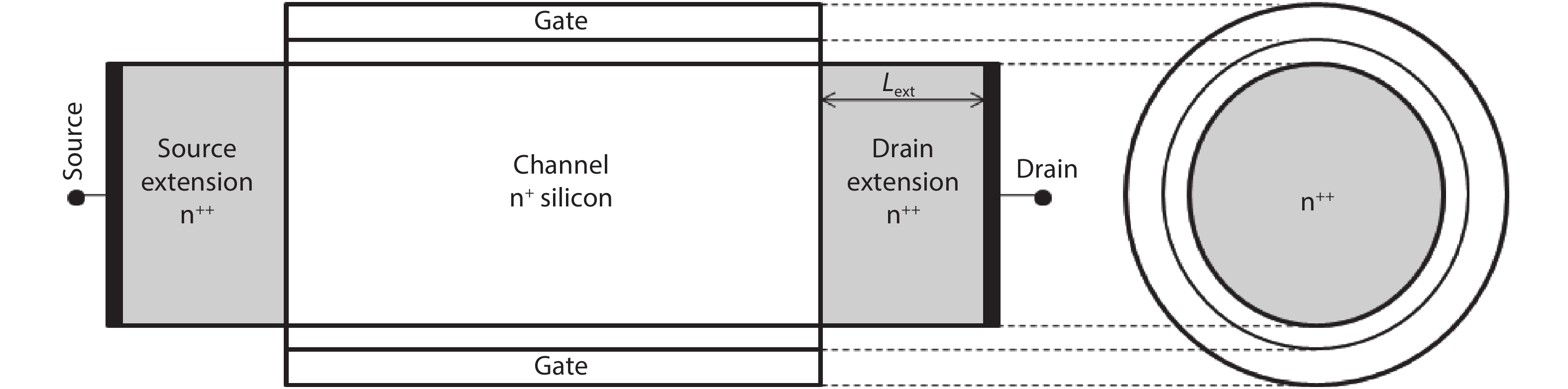
Fig. 1.
TM-DG MOSFET structure.
REVIEWS
Namrata Mendiratta and Suman Lata Tripathi
Corresponding author: Suman Lata Tripathi, tri.suman78@gmail.com
Abstract: CMOS technology is one of the most frequently used technologies in the semiconductor industry as it can be successfully integrated with ICs. Every two years the number of MOS transistors doubles because the size of the MOSFET is reduced. Reducing the size of the MOSFET reduces the size of the channel length which causes short channel effects and it increases the leakage current. To reduce the short channel effects new designs and technologies are implemented. Double gate MOSFET design has shown improvement in performance as amplifiers over a single MOSFET. Silicon-based MOSFET design can be used in a harsh environment. It has been used in various applications such as in detecting biomolecules. The increase in number of gates increases the current drive capability of transistors. GAA MOSFET is an example of a quadruple gate around the four sides of channel that increases gate control over the channel region. It also increases effective channel width that improves drain current and reduces leakage current keeping short channel effects under limit. Junctionless MOSFET operates faster and uses less power with increase in ON-state current leading to a good value of ION/IOFF ratio. In this paper, several gate and channel engineered MOSFET structures are analyzed and compared for sub 45 nm technology node. A comparison among different MOSFET structures has been made for subthreshold performance parameters in terms of IOFF, subthreshold slope and DIBL values. The analog/RF performance is analyzed for transconductance, effective transistor capacitances, stability factor and critical frequency. The paper also covers different applications of advance MOSFET structures in analog/digital or IoT/ biomedical applications.
Key words: MOSFET, junctionless, RF, biosensor, DIBL, double gate
| [1] |
Radamson H H. CMOS past, present and future. Woodhead Publishing Series in Electronic and Optical Materials, 2018
|
| [2] |
Buvaneswari B, Balamurugan N B. 2D analytical modeling and simulation of dual material DG MOSFET for biosensing application. Int J Electron Commun, 2019, 99, 193 doi: 10.1016/j.aeue.2018.11.039
|
| [3] |
Srivastava V M, Yadav K S, Singh G. Design and performance analysis of double-gate MOSFET over single-gate MOSFET for RF switch. Microelectron J, 2012, 43(9), 873 doi: 10.1016/j.mejo.2010.12.007
|
| [4] |
Colinge J P. Multi-gate SOI MOSFETs. Microelectron Eng, 2007, 84, 2071 doi: 10.1016/j.mee.2007.04.038
|
| [5] |
Gili E, Kunz V D, Groot C H D, et al. Single, double and surround gate vertical MOSFETs with reduced parasitic capacitance. Solid-State Electron, 2004, 48, 511 doi: 10.1016/j.sse.2003.09.019
|
| [6] |
Verma J H K, Pratap Y, Haldar S, et al. Capacitance modeling of gate material engineered cylindrical/surrounded gate MOSFETs for sensor applications. Superlattices Microstruct, 2015, 88, 271 doi: 10.1016/j.spmi.2015.09.015
|
| [7] |
Tienda-Luna I M, Roldan J B, Ruiz F G, et al. An analytical mobility model for square gate-all-around MOSFETs. Solid-State Electron, 2013, 90, 18 doi: 10.1016/j.sse.2013.02.058
|
| [8] |
Djeffal F, Ferhati H, Bentrcia T. Improved analog and RF performances of gate-all-around junctionless MOSFET with drain and source extensions. Superlattices Microstruct, 2016, 90, 193 doi: 10.1016/j.spmi.2015.09.041
|
| [9] |
Sarkar A, Das A K, De S, et al. Effect of gate engineering in double-gate MOSFETs for analog/RF applications. Microelectron J, 2012, 43, 873 doi: 10.1016/j.mejo.2012.06.002
|
| [10] |
Nasri F, Aissa M F B, Gazzah M H, et al. 3D thermal conduction in ananoscale tri-Gate MOSFET based on single-phase-lag model. Appl Therm Eng, 2015, 91(5), 647 doi: 10.1016/j.applthermaleng.2015.08.045
|
| [11] |
Pakaree J E, Srivastava V M. Realization with fabrication of double-gate MOSFET based differential amplifier. Microelectron J, 2019, 91, 70 doi: 10.1016/j.mejo.2019.07.012
|
| [12] |
Abhinav, Rai S. Reliability analysis of junction-less double gate (JLDG) MOSFET for analog/RF circuits for high linearity applications. Microelectron J, 2017, 64, 60 doi: 10.1016/j.mejo.2017.04.009
|
| [13] |
Srivastava V M, Yadav K S, Singh G. Design and performance analysis of cylindrical surrounding double-gate MOSFET for RF switch. Microelectron J, 2011, 42, 1124 doi: 10.1016/j.mejo.2011.07.003
|
| [14] |
Ku W H. Unilateral gain and stability criterion of active two-ports in terms of scattering parameters. Proc IEEE, 1966, 54(11), 1617 doi: 10.1109/PROC.1966.5229
|
| [15] |
Sivasankaran K, Kannadassan D, Seetaram K, et al. Bias and geometry optimization of silicon nanowire transistor: radio frequency stability perspective. Micro Optic Technol Lett, 2012, 54(9), 2114 doi: 10.1002/mop.27016
|
| [16] |
Orouji A A, Heydari S, Fathipour M. Double step buried oxide (DSBO) SOI-MOSFET: A proposed structure for improving self-heating effects. Physica E, 2009, 41, 1665 doi: 10.1016/j.physe.2009.05.017
|
| [17] |
Kwona I, Kwonb H I, Cho H I. Development of high temperatureoperation silicon based MOSFET for harsh environment application. Results Phys, 2018, 11, 475 doi: 10.1016/j.rinp.2018.09.035
|
| [18] |
Tahirparveen. Operational transconductance amplifier and analog integrated circuits. I K International Publishing House, 2009
|
| [19] |
Narang R, Saxena M, Gupta M. Modeling of gate underlap junctionless double gate MOSFET as bio-sensor. Mater Sci Semicond Process, 2017, 71, 240 doi: 10.1016/j.mssp.2017.08.008
|
| [20] |
Kumar A, Tripathi M M, Chaujar R. Comprehensive analysis of sub-20 nm black phosphorus based junctionless-recessed channel MOSFET for analog/RF applications. Superlattices Microstruct, 2018, 116, 171 doi: 10.1016/j.spmi.2018.02.018
|
| [21] |
Djeffal F, Lakhdar N, Yousfi A. An optimized design of 10-nm-scale dual-material surrounded gate MOSFETs for digital circuit applications. Physica E, 2011, 44, 339 doi: 10.1016/j.physe.2011.09.007
|
| [22] |
Pathak V, Saini G. A Graded channel dual-material gate junctionless MOSFET for analog applications. Proced Comput Sci, 2018, 125, 825 doi: 10.1016/j.procs.2017.12.105
|
| [23] |
Narang R, Saxena M, Gupta M. Investigation of dielectric modulated (DM) double gate (DG) junctionless MOSFETs for application as a biosensors. Superlattices Microstruct, 2015, 85, 557 doi: 10.1016/j.spmi.2015.04.040
|
| [24] |
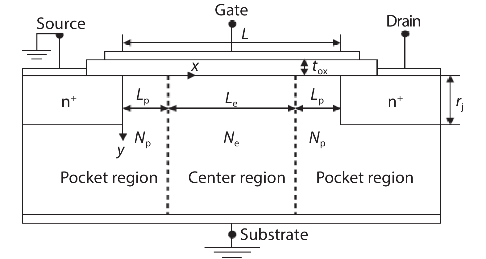
Pang Y S, Brews J R. Design of 0.1-μm pocket n-MOSFETs for low-voltage applications. Solid-State Electron, 2002, 46, 2315 doi: 10.1016/S0038-1101(02)00226-5
|
| [25] |
Orouji A A, Kumar M J. Nanoscale SOI MOSFETs with electrically induced source/drain extension: Novel attributes and design considerations for suppressed short-channel effects. Superlattices Microstruct, 2006, 39, 395 doi: 10.1016/j.spmi.2005.08.020
|
| [26] |
Pal A, Sarkar A. Analytical study of dual material surrounding gate MOSFET to suppress short-channel effects (SCEs). Eng Sci Technol, 2014, 17, 205 doi: 10.1016/j.jestch.2014.06.002
|
| [27] |
Chebaki E, Djeffal F, Ferhati H, et al. Improved analog/RF performance of double gate junctionless MOSFET using both gate material engineering and drain/source extensions. Superlattices Microstruct, 2016, 92, 80 doi: 10.1016/j.spmi.2016.02.009
|
| [28] |
Wang Y, Tang Y, Sun L L, et al. High performance of junctionless MOSFET with asymmetric gate. Superlattices Microstruct, 2016, 97, 2016 doi: 10.1016/j.spmi.2016.06.003
|
| [29] |
Awadhiya B, Kondekar P N, Meshram A D. Understanding negative differential resistance and region of operation in undoped HfO2-based negative capacitance field effect transistor. Appl Phys A, 2019, 125, 427 doi: 10.1007/s00339-019-2718-2
|
| [30] |
Kumar A, Gupta N, Chaujar R. TCAD RF performance investigation of transparent gate recessed channel MOSFET. Microelectron J, 2016, 49, 36 doi: 10.1016/j.mejo.2015.12.007
|
| [31] |
Mishra V K, Chauhan R K. Efficient layout design of junctionless transistor based 6-T SRAM cell using SOI technology. ECS J Solid State Sci Technol, 2018, 9, 456 doi: 10.1149/2.0061809jss
|
| [32] |
Roy N C, Gupta A, Rai S. Analytical surface potential modeling and simulation of junction-less double gate (JLDG) MOSFET for ultra-low power analog/RF circuits. Microelectron J, 2015, 46, 916 doi: 10.1016/j.mejo.2015.07.009
|
| [33] |
Saramekala G K, Santra A, Dubey S, et al. An analytical threshold voltage model for a short-channel dual-metal-gate (DMG) recessed-source/drain (Re-S/D) SOI MOSFET. Superlattices Microstruct, 2013, 60, 580 doi: 10.1016/j.spmi.2013.05.022
|
| [34] |
Tripathi S L, Patel R, Agrawal V K. Low leakage pocket junction-less DGTFET with bio sensing cavity region. Turk J Electr Eng Comput Sci, 2019, 27(4), 2466 doi: 10.3906/elk-1807-186
|

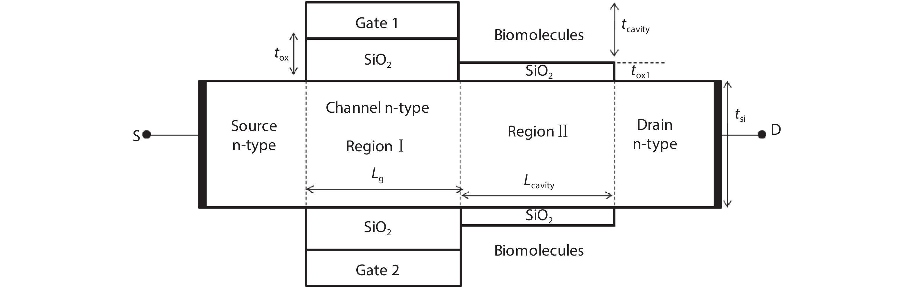
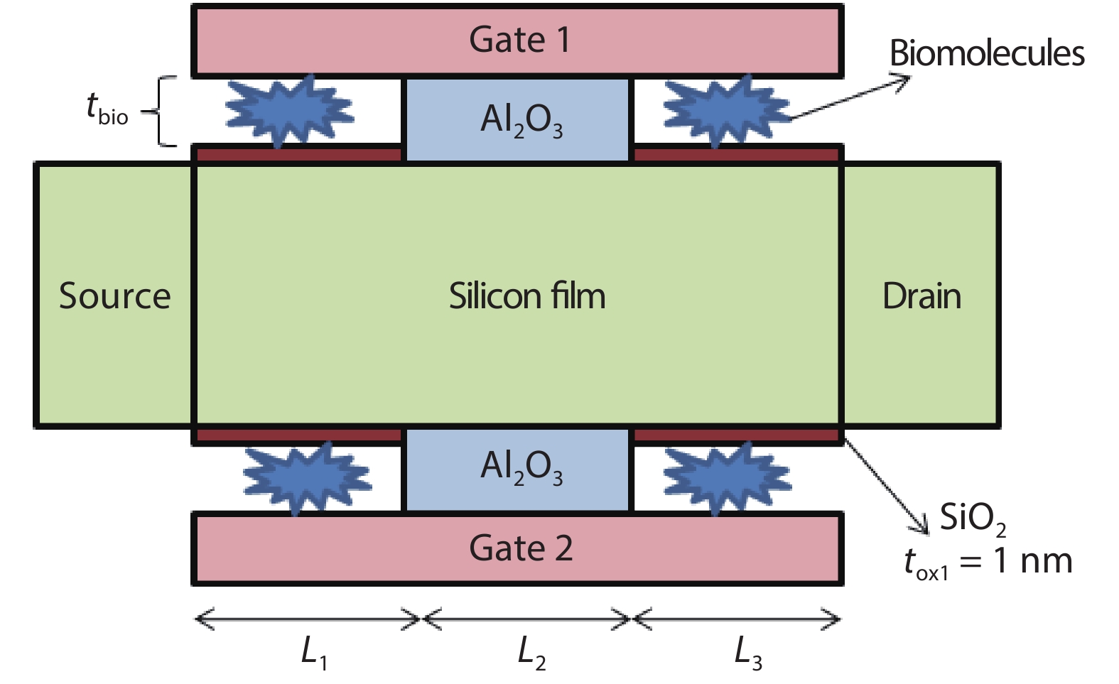


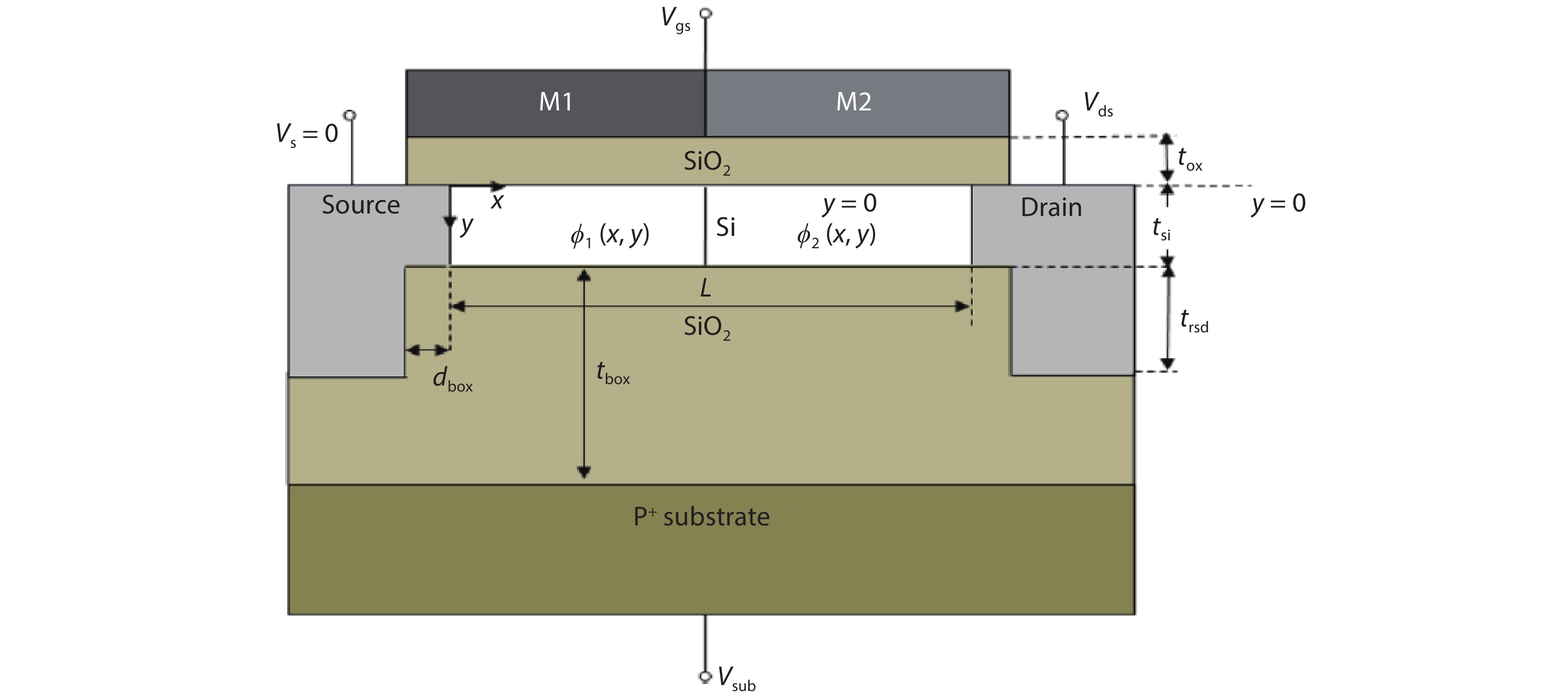
Table 1. Comparison of performance parameters of different MOSFET structures.
| Parameter | ION (A/μm) | IOFF (A/μm) | ION/IOFF | SS (mV/dec) | DIBL (mV/V) | Channel length (nm) | Application |
| (GC-DMGJL) MOSFET[22] | 7.695 × 10⁻⁴ | 3.741 × 10⁻¹⁰ | 2.057 × 10⁶ | 73.42 | 21 | 15 | Analog circuit |
| AG-JL MOSFET[28] | 127 × 10–4 | 1 × 10–15 | 1.27 × 10⁵ | 68 | 65 | 20 | Digital circuit |
| (DMSG) MOSFET[21] | – | 1.053 × 10⁻¹⁶ | – | 64.7978 | – | 10 | Digital circuit |
| JLDG[32] | – | – | 4.86 × 10⁹ | 62.32 | 75.98 | 20 | Analog/RF |
| DGJL MOSFET[27] | – | – | 4.03 × 10⁹ | 63.34 | 79.58 | 20 | Analog/RF |
 DownLoad: CSV
| [1] |
Radamson H H. CMOS past, present and future. Woodhead Publishing Series in Electronic and Optical Materials, 2018
|
| [2] |
Buvaneswari B, Balamurugan N B. 2D analytical modeling and simulation of dual material DG MOSFET for biosensing application. Int J Electron Commun, 2019, 99, 193 doi: 10.1016/j.aeue.2018.11.039
|
| [3] |
Srivastava V M, Yadav K S, Singh G. Design and performance analysis of double-gate MOSFET over single-gate MOSFET for RF switch. Microelectron J, 2012, 43(9), 873 doi: 10.1016/j.mejo.2010.12.007
|
| [4] |
Colinge J P. Multi-gate SOI MOSFETs. Microelectron Eng, 2007, 84, 2071 doi: 10.1016/j.mee.2007.04.038
|
| [5] |
Gili E, Kunz V D, Groot C H D, et al. Single, double and surround gate vertical MOSFETs with reduced parasitic capacitance. Solid-State Electron, 2004, 48, 511 doi: 10.1016/j.sse.2003.09.019
|
| [6] |
Verma J H K, Pratap Y, Haldar S, et al. Capacitance modeling of gate material engineered cylindrical/surrounded gate MOSFETs for sensor applications. Superlattices Microstruct, 2015, 88, 271 doi: 10.1016/j.spmi.2015.09.015
|
| [7] |
Tienda-Luna I M, Roldan J B, Ruiz F G, et al. An analytical mobility model for square gate-all-around MOSFETs. Solid-State Electron, 2013, 90, 18 doi: 10.1016/j.sse.2013.02.058
|
| [8] |
Djeffal F, Ferhati H, Bentrcia T. Improved analog and RF performances of gate-all-around junctionless MOSFET with drain and source extensions. Superlattices Microstruct, 2016, 90, 193 doi: 10.1016/j.spmi.2015.09.041
|
| [9] |
Sarkar A, Das A K, De S, et al. Effect of gate engineering in double-gate MOSFETs for analog/RF applications. Microelectron J, 2012, 43, 873 doi: 10.1016/j.mejo.2012.06.002
|
| [10] |
Nasri F, Aissa M F B, Gazzah M H, et al. 3D thermal conduction in ananoscale tri-Gate MOSFET based on single-phase-lag model. Appl Therm Eng, 2015, 91(5), 647 doi: 10.1016/j.applthermaleng.2015.08.045
|
| [11] |
Pakaree J E, Srivastava V M. Realization with fabrication of double-gate MOSFET based differential amplifier. Microelectron J, 2019, 91, 70 doi: 10.1016/j.mejo.2019.07.012
|
| [12] |
Abhinav, Rai S. Reliability analysis of junction-less double gate (JLDG) MOSFET for analog/RF circuits for high linearity applications. Microelectron J, 2017, 64, 60 doi: 10.1016/j.mejo.2017.04.009
|
| [13] |
Srivastava V M, Yadav K S, Singh G. Design and performance analysis of cylindrical surrounding double-gate MOSFET for RF switch. Microelectron J, 2011, 42, 1124 doi: 10.1016/j.mejo.2011.07.003
|
| [14] |
Ku W H. Unilateral gain and stability criterion of active two-ports in terms of scattering parameters. Proc IEEE, 1966, 54(11), 1617 doi: 10.1109/PROC.1966.5229
|
| [15] |
Sivasankaran K, Kannadassan D, Seetaram K, et al. Bias and geometry optimization of silicon nanowire transistor: radio frequency stability perspective. Micro Optic Technol Lett, 2012, 54(9), 2114 doi: 10.1002/mop.27016
|
| [16] |
Orouji A A, Heydari S, Fathipour M. Double step buried oxide (DSBO) SOI-MOSFET: A proposed structure for improving self-heating effects. Physica E, 2009, 41, 1665 doi: 10.1016/j.physe.2009.05.017
|
| [17] |
Kwona I, Kwonb H I, Cho H I. Development of high temperatureoperation silicon based MOSFET for harsh environment application. Results Phys, 2018, 11, 475 doi: 10.1016/j.rinp.2018.09.035
|
| [18] |
Tahirparveen. Operational transconductance amplifier and analog integrated circuits. I K International Publishing House, 2009
|
| [19] |
Narang R, Saxena M, Gupta M. Modeling of gate underlap junctionless double gate MOSFET as bio-sensor. Mater Sci Semicond Process, 2017, 71, 240 doi: 10.1016/j.mssp.2017.08.008
|
| [20] |
Kumar A, Tripathi M M, Chaujar R. Comprehensive analysis of sub-20 nm black phosphorus based junctionless-recessed channel MOSFET for analog/RF applications. Superlattices Microstruct, 2018, 116, 171 doi: 10.1016/j.spmi.2018.02.018
|
| [21] |
Djeffal F, Lakhdar N, Yousfi A. An optimized design of 10-nm-scale dual-material surrounded gate MOSFETs for digital circuit applications. Physica E, 2011, 44, 339 doi: 10.1016/j.physe.2011.09.007
|
| [22] |
Pathak V, Saini G. A Graded channel dual-material gate junctionless MOSFET for analog applications. Proced Comput Sci, 2018, 125, 825 doi: 10.1016/j.procs.2017.12.105
|
| [23] |
Narang R, Saxena M, Gupta M. Investigation of dielectric modulated (DM) double gate (DG) junctionless MOSFETs for application as a biosensors. Superlattices Microstruct, 2015, 85, 557 doi: 10.1016/j.spmi.2015.04.040
|
| [24] |
Pang Y S, Brews J R. Design of 0.1-μm pocket n-MOSFETs for low-voltage applications. Solid-State Electron, 2002, 46, 2315 doi: 10.1016/S0038-1101(02)00226-5
|
| [25] |
Orouji A A, Kumar M J. Nanoscale SOI MOSFETs with electrically induced source/drain extension: Novel attributes and design considerations for suppressed short-channel effects. Superlattices Microstruct, 2006, 39, 395 doi: 10.1016/j.spmi.2005.08.020
|
| [26] |
Pal A, Sarkar A. Analytical study of dual material surrounding gate MOSFET to suppress short-channel effects (SCEs). Eng Sci Technol, 2014, 17, 205 doi: 10.1016/j.jestch.2014.06.002
|
| [27] |
Chebaki E, Djeffal F, Ferhati H, et al. Improved analog/RF performance of double gate junctionless MOSFET using both gate material engineering and drain/source extensions. Superlattices Microstruct, 2016, 92, 80 doi: 10.1016/j.spmi.2016.02.009
|
| [28] |
Wang Y, Tang Y, Sun L L, et al. High performance of junctionless MOSFET with asymmetric gate. Superlattices Microstruct, 2016, 97, 2016 doi: 10.1016/j.spmi.2016.06.003
|
| [29] |
Awadhiya B, Kondekar P N, Meshram A D. Understanding negative differential resistance and region of operation in undoped HfO2-based negative capacitance field effect transistor. Appl Phys A, 2019, 125, 427 doi: 10.1007/s00339-019-2718-2
|
| [30] |
Kumar A, Gupta N, Chaujar R. TCAD RF performance investigation of transparent gate recessed channel MOSFET. Microelectron J, 2016, 49, 36 doi: 10.1016/j.mejo.2015.12.007
|
| [31] |
Mishra V K, Chauhan R K. Efficient layout design of junctionless transistor based 6-T SRAM cell using SOI technology. ECS J Solid State Sci Technol, 2018, 9, 456 doi: 10.1149/2.0061809jss
|
| [32] |
Roy N C, Gupta A, Rai S. Analytical surface potential modeling and simulation of junction-less double gate (JLDG) MOSFET for ultra-low power analog/RF circuits. Microelectron J, 2015, 46, 916 doi: 10.1016/j.mejo.2015.07.009
|
| [33] |
Saramekala G K, Santra A, Dubey S, et al. An analytical threshold voltage model for a short-channel dual-metal-gate (DMG) recessed-source/drain (Re-S/D) SOI MOSFET. Superlattices Microstruct, 2013, 60, 580 doi: 10.1016/j.spmi.2013.05.022
|
| [34] |
Tripathi S L, Patel R, Agrawal V K. Low leakage pocket junction-less DGTFET with bio sensing cavity region. Turk J Electr Eng Comput Sci, 2019, 27(4), 2466 doi: 10.3906/elk-1807-186
|


Article views: 8982 Times PDF downloads: 524 Times Cited by: 0 Times
Received: 04 November 2019 Revised: 18 November 2019 Online: Accepted Manuscript: 13 January 2020Uncorrected proof: 15 January 2020Published: 01 June 2020
| Citation: |
Namrata Mendiratta, Suman Lata Tripathi. A review on performance comparison of advanced MOSFET structures below 45 nm technology node[J]. Journal of Semiconductors, 2020, 41(6): 061401. doi: 10.1088/1674-4926/41/6/061401
****
N Mendiratta, S L Tripathi, A review on performance comparison of advanced MOSFET structures below 45 nm technology node[J]. J. Semicond., 2020, 41(6): 061401. doi: 10.1088/1674-4926/41/6/061401.

|
| [1] |
Radamson H H. CMOS past, present and future. Woodhead Publishing Series in Electronic and Optical Materials, 2018
|
| [2] |
Buvaneswari B, Balamurugan N B. 2D analytical modeling and simulation of dual material DG MOSFET for biosensing application. Int J Electron Commun, 2019, 99, 193 doi: 10.1016/j.aeue.2018.11.039
|
| [3] |
Srivastava V M, Yadav K S, Singh G. Design and performance analysis of double-gate MOSFET over single-gate MOSFET for RF switch. Microelectron J, 2012, 43(9), 873 doi: 10.1016/j.mejo.2010.12.007
|
| [4] |
Colinge J P. Multi-gate SOI MOSFETs. Microelectron Eng, 2007, 84, 2071 doi: 10.1016/j.mee.2007.04.038
|
| [5] |
Gili E, Kunz V D, Groot C H D, et al. Single, double and surround gate vertical MOSFETs with reduced parasitic capacitance. Solid-State Electron, 2004, 48, 511 doi: 10.1016/j.sse.2003.09.019
|
| [6] |
Verma J H K, Pratap Y, Haldar S, et al. Capacitance modeling of gate material engineered cylindrical/surrounded gate MOSFETs for sensor applications. Superlattices Microstruct, 2015, 88, 271 doi: 10.1016/j.spmi.2015.09.015
|
| [7] |
Tienda-Luna I M, Roldan J B, Ruiz F G, et al. An analytical mobility model for square gate-all-around MOSFETs. Solid-State Electron, 2013, 90, 18 doi: 10.1016/j.sse.2013.02.058
|
| [8] |
Djeffal F, Ferhati H, Bentrcia T. Improved analog and RF performances of gate-all-around junctionless MOSFET with drain and source extensions. Superlattices Microstruct, 2016, 90, 193 doi: 10.1016/j.spmi.2015.09.041
|
| [9] |
Sarkar A, Das A K, De S, et al. Effect of gate engineering in double-gate MOSFETs for analog/RF applications. Microelectron J, 2012, 43, 873 doi: 10.1016/j.mejo.2012.06.002
|
| [10] |
Nasri F, Aissa M F B, Gazzah M H, et al. 3D thermal conduction in ananoscale tri-Gate MOSFET based on single-phase-lag model. Appl Therm Eng, 2015, 91(5), 647 doi: 10.1016/j.applthermaleng.2015.08.045
|
| [11] |
Pakaree J E, Srivastava V M. Realization with fabrication of double-gate MOSFET based differential amplifier. Microelectron J, 2019, 91, 70 doi: 10.1016/j.mejo.2019.07.012
|
| [12] |
Abhinav, Rai S. Reliability analysis of junction-less double gate (JLDG) MOSFET for analog/RF circuits for high linearity applications. Microelectron J, 2017, 64, 60 doi: 10.1016/j.mejo.2017.04.009
|
| [13] |
Srivastava V M, Yadav K S, Singh G. Design and performance analysis of cylindrical surrounding double-gate MOSFET for RF switch. Microelectron J, 2011, 42, 1124 doi: 10.1016/j.mejo.2011.07.003
|
| [14] |
Ku W H. Unilateral gain and stability criterion of active two-ports in terms of scattering parameters. Proc IEEE, 1966, 54(11), 1617 doi: 10.1109/PROC.1966.5229
|
| [15] |
Sivasankaran K, Kannadassan D, Seetaram K, et al. Bias and geometry optimization of silicon nanowire transistor: radio frequency stability perspective. Micro Optic Technol Lett, 2012, 54(9), 2114 doi: 10.1002/mop.27016
|
| [16] |
Orouji A A, Heydari S, Fathipour M. Double step buried oxide (DSBO) SOI-MOSFET: A proposed structure for improving self-heating effects. Physica E, 2009, 41, 1665 doi: 10.1016/j.physe.2009.05.017
|
| [17] |
Kwona I, Kwonb H I, Cho H I. Development of high temperatureoperation silicon based MOSFET for harsh environment application. Results Phys, 2018, 11, 475 doi: 10.1016/j.rinp.2018.09.035
|
| [18] |
Tahirparveen. Operational transconductance amplifier and analog integrated circuits. I K International Publishing House, 2009
|
| [19] |
Narang R, Saxena M, Gupta M. Modeling of gate underlap junctionless double gate MOSFET as bio-sensor. Mater Sci Semicond Process, 2017, 71, 240 doi: 10.1016/j.mssp.2017.08.008
|
| [20] |
Kumar A, Tripathi M M, Chaujar R. Comprehensive analysis of sub-20 nm black phosphorus based junctionless-recessed channel MOSFET for analog/RF applications. Superlattices Microstruct, 2018, 116, 171 doi: 10.1016/j.spmi.2018.02.018
|
| [21] |
Djeffal F, Lakhdar N, Yousfi A. An optimized design of 10-nm-scale dual-material surrounded gate MOSFETs for digital circuit applications. Physica E, 2011, 44, 339 doi: 10.1016/j.physe.2011.09.007
|
| [22] |
Pathak V, Saini G. A Graded channel dual-material gate junctionless MOSFET for analog applications. Proced Comput Sci, 2018, 125, 825 doi: 10.1016/j.procs.2017.12.105
|
| [23] |
Narang R, Saxena M, Gupta M. Investigation of dielectric modulated (DM) double gate (DG) junctionless MOSFETs for application as a biosensors. Superlattices Microstruct, 2015, 85, 557 doi: 10.1016/j.spmi.2015.04.040
|
| [24] |
Pang Y S, Brews J R. Design of 0.1-μm pocket n-MOSFETs for low-voltage applications. Solid-State Electron, 2002, 46, 2315 doi: 10.1016/S0038-1101(02)00226-5
|
| [25] |
Orouji A A, Kumar M J. Nanoscale SOI MOSFETs with electrically induced source/drain extension: Novel attributes and design considerations for suppressed short-channel effects. Superlattices Microstruct, 2006, 39, 395 doi: 10.1016/j.spmi.2005.08.020
|
| [26] |
Pal A, Sarkar A. Analytical study of dual material surrounding gate MOSFET to suppress short-channel effects (SCEs). Eng Sci Technol, 2014, 17, 205 doi: 10.1016/j.jestch.2014.06.002
|
| [27] |
Chebaki E, Djeffal F, Ferhati H, et al. Improved analog/RF performance of double gate junctionless MOSFET using both gate material engineering and drain/source extensions. Superlattices Microstruct, 2016, 92, 80 doi: 10.1016/j.spmi.2016.02.009
|
| [28] |
Wang Y, Tang Y, Sun L L, et al. High performance of junctionless MOSFET with asymmetric gate. Superlattices Microstruct, 2016, 97, 2016 doi: 10.1016/j.spmi.2016.06.003
|
| [29] |
Awadhiya B, Kondekar P N, Meshram A D. Understanding negative differential resistance and region of operation in undoped HfO2-based negative capacitance field effect transistor. Appl Phys A, 2019, 125, 427 doi: 10.1007/s00339-019-2718-2
|
| [30] |
Kumar A, Gupta N, Chaujar R. TCAD RF performance investigation of transparent gate recessed channel MOSFET. Microelectron J, 2016, 49, 36 doi: 10.1016/j.mejo.2015.12.007
|
| [31] |
Mishra V K, Chauhan R K. Efficient layout design of junctionless transistor based 6-T SRAM cell using SOI technology. ECS J Solid State Sci Technol, 2018, 9, 456 doi: 10.1149/2.0061809jss
|
| [32] |
Roy N C, Gupta A, Rai S. Analytical surface potential modeling and simulation of junction-less double gate (JLDG) MOSFET for ultra-low power analog/RF circuits. Microelectron J, 2015, 46, 916 doi: 10.1016/j.mejo.2015.07.009
|
| [33] |
Saramekala G K, Santra A, Dubey S, et al. An analytical threshold voltage model for a short-channel dual-metal-gate (DMG) recessed-source/drain (Re-S/D) SOI MOSFET. Superlattices Microstruct, 2013, 60, 580 doi: 10.1016/j.spmi.2013.05.022
|
| [34] |
Tripathi S L, Patel R, Agrawal V K. Low leakage pocket junction-less DGTFET with bio sensing cavity region. Turk J Electr Eng Comput Sci, 2019, 27(4), 2466 doi: 10.3906/elk-1807-186
|

 WeChat ID
Journal of Semiconductors © 2017 All Rights Reserved 京ICP备05085259号-2