Issue Browser
Volume 41, Issue 6,
Jun 2020
Column

J. Semicond.
2020, 41(6): 061101 doi: 10.1088/1674-4926/41/6/061101
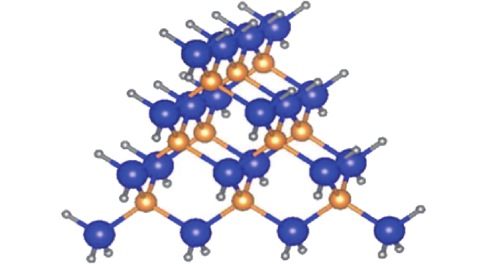
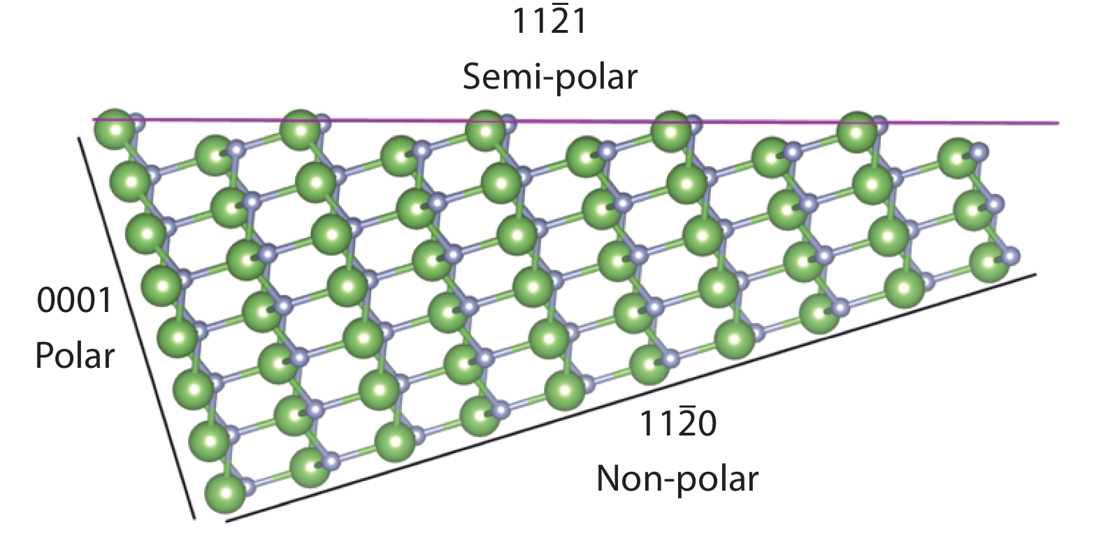
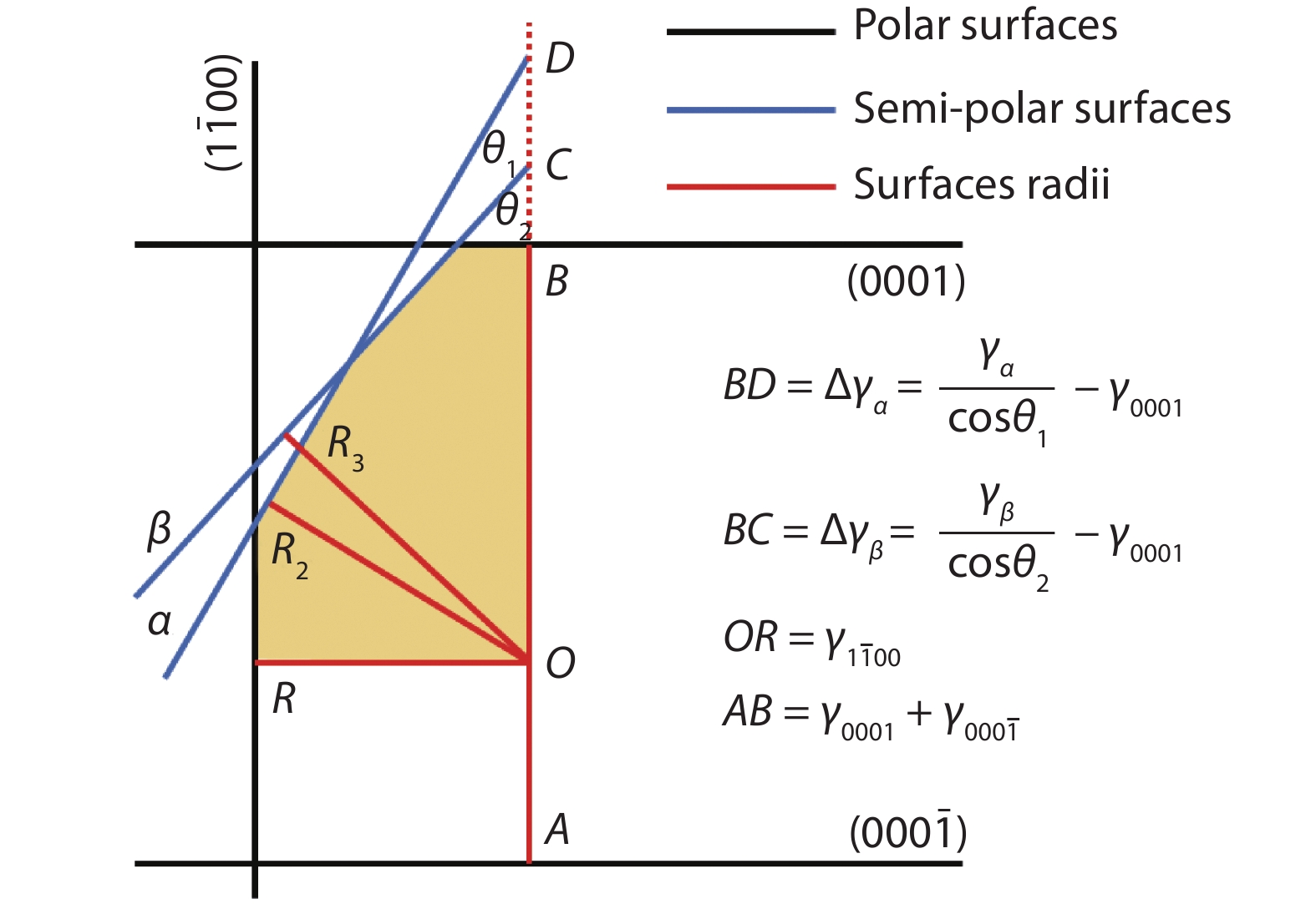
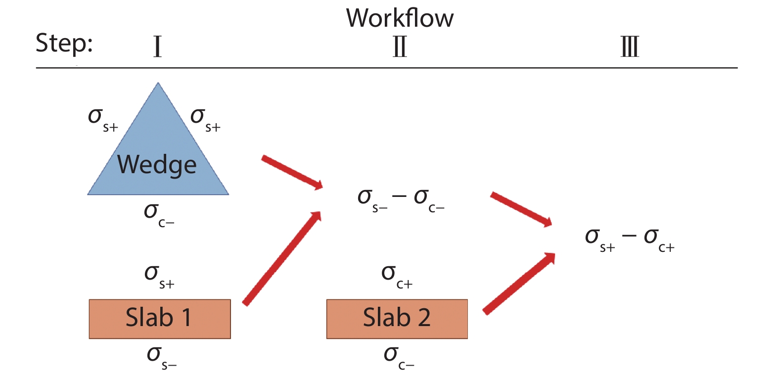
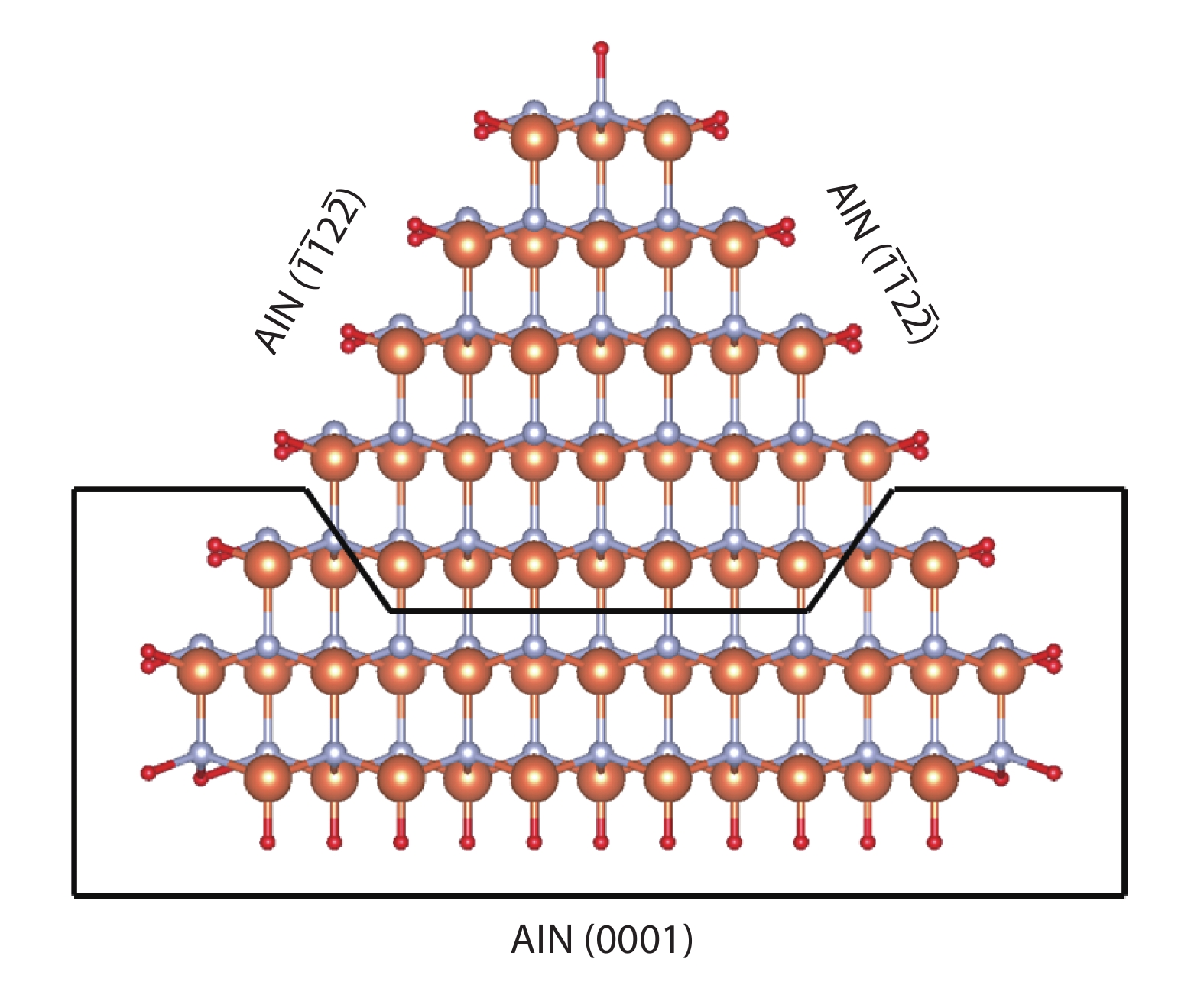
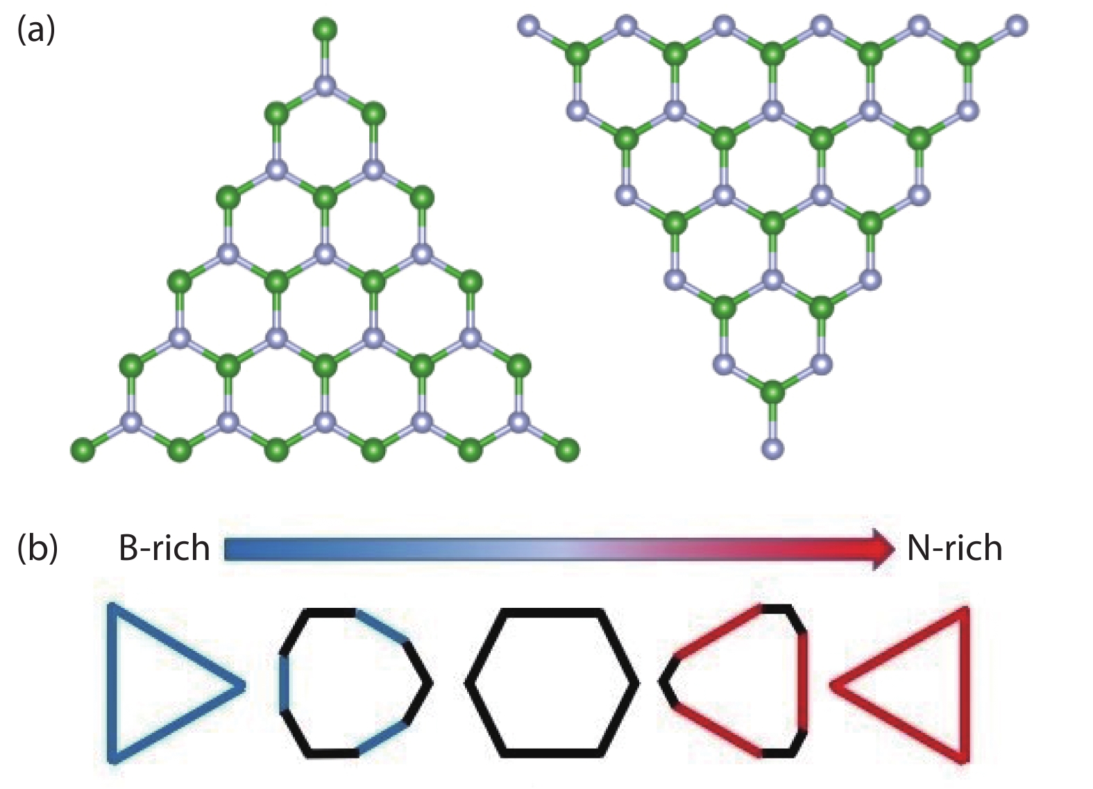
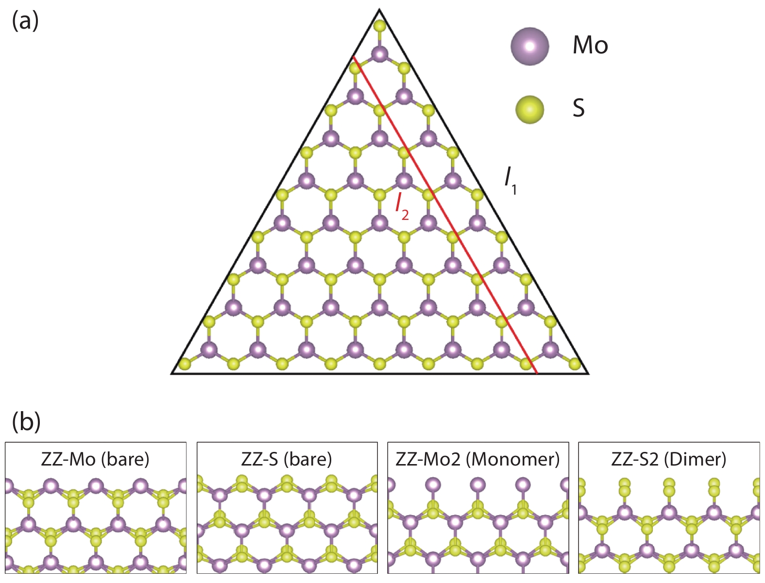
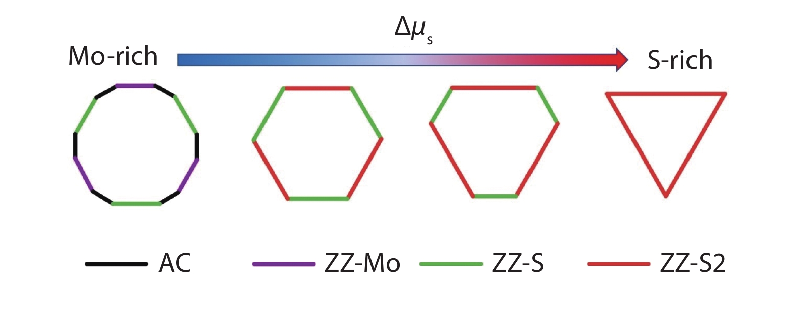
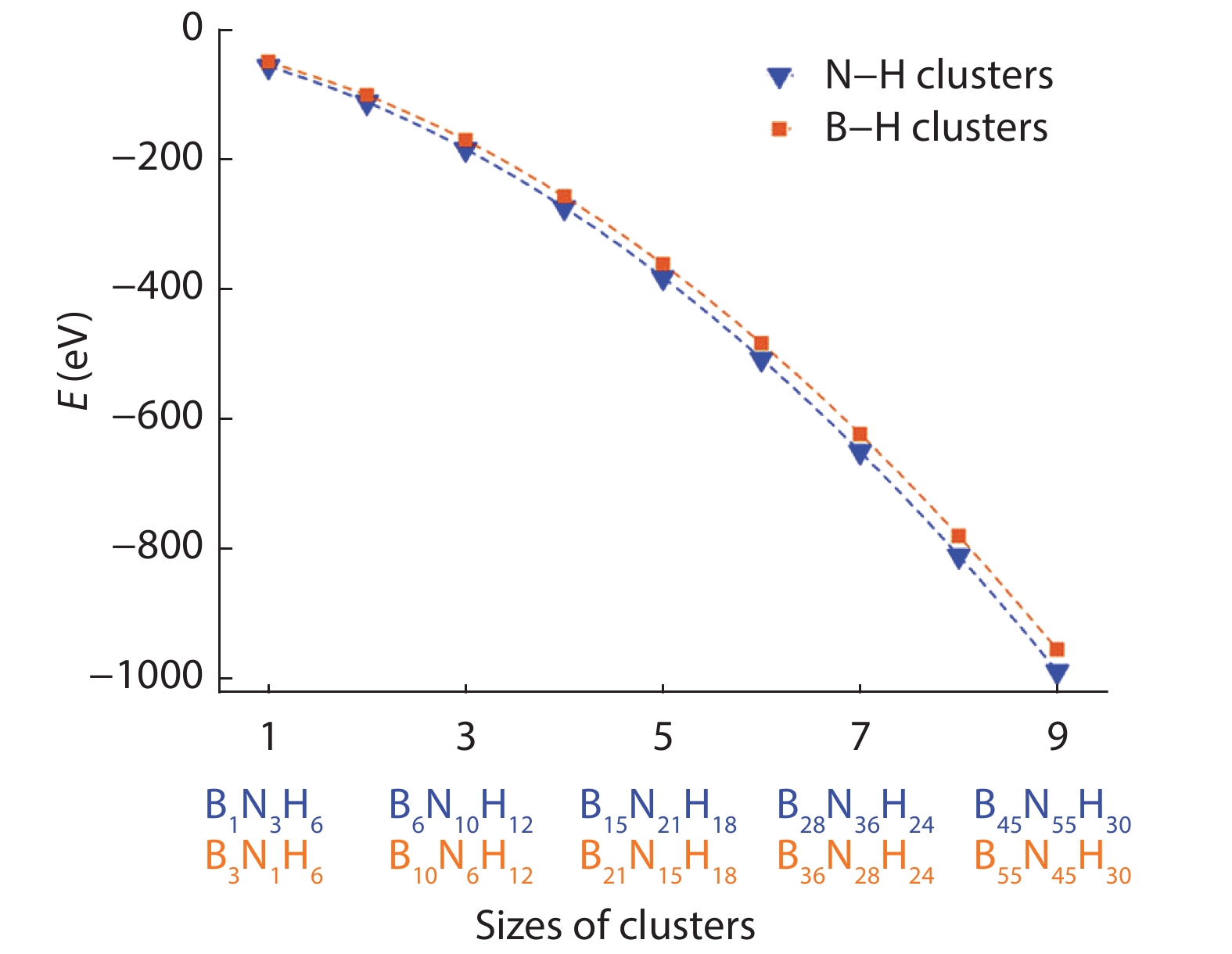
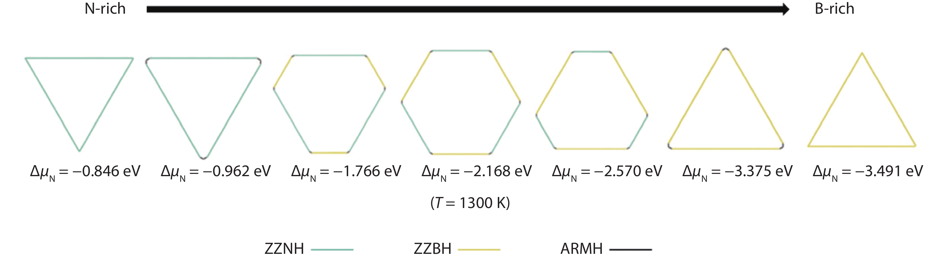
To have a high quality experimental growth of crystals, understanding the equilibrium crystal shape (ECS) in different thermodynamic growth conditions is important. The factor governing the ECS is usually the absolute surface formation energies for surfaces (or edges in 2D) in different orientations. Therefore, it is necessary to obtain an accurate value of these energies in order to give a good explanation for the observation in growth experiment. Historically, there have been different approaches proposed to solve this problem. This paper is going to review these representative literatures and discuss the pitfalls and advantages of different methods.


J. Semicond.
2020, 41(6): 061401 doi: 10.1088/1674-4926/41/6/061401
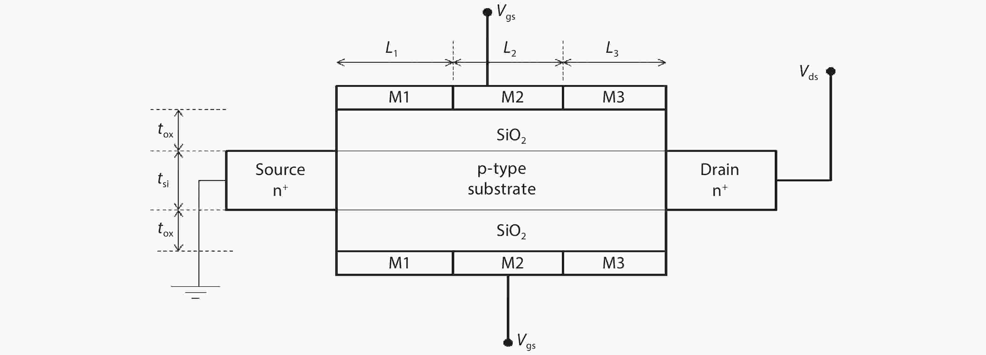
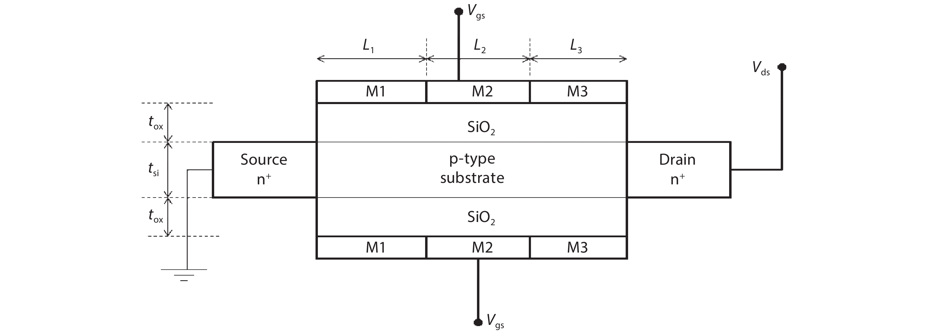
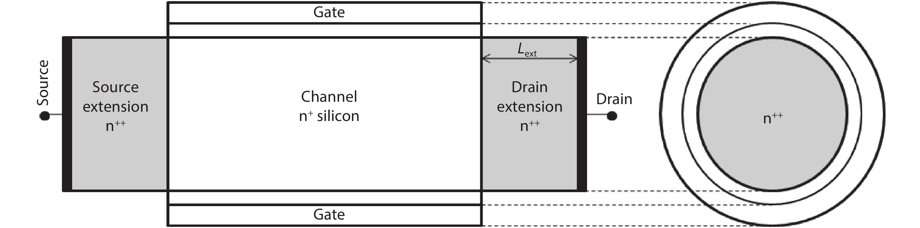
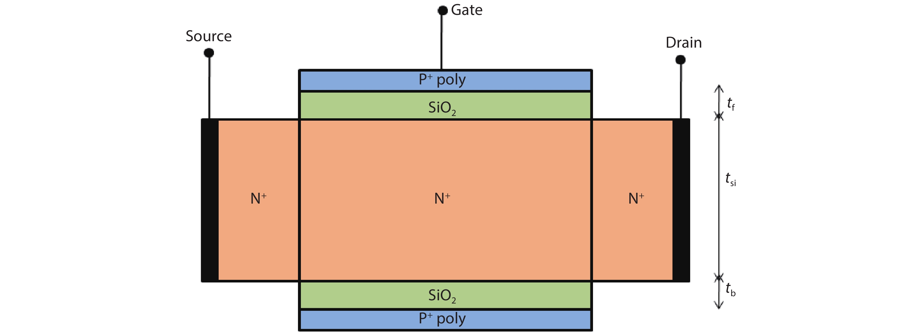
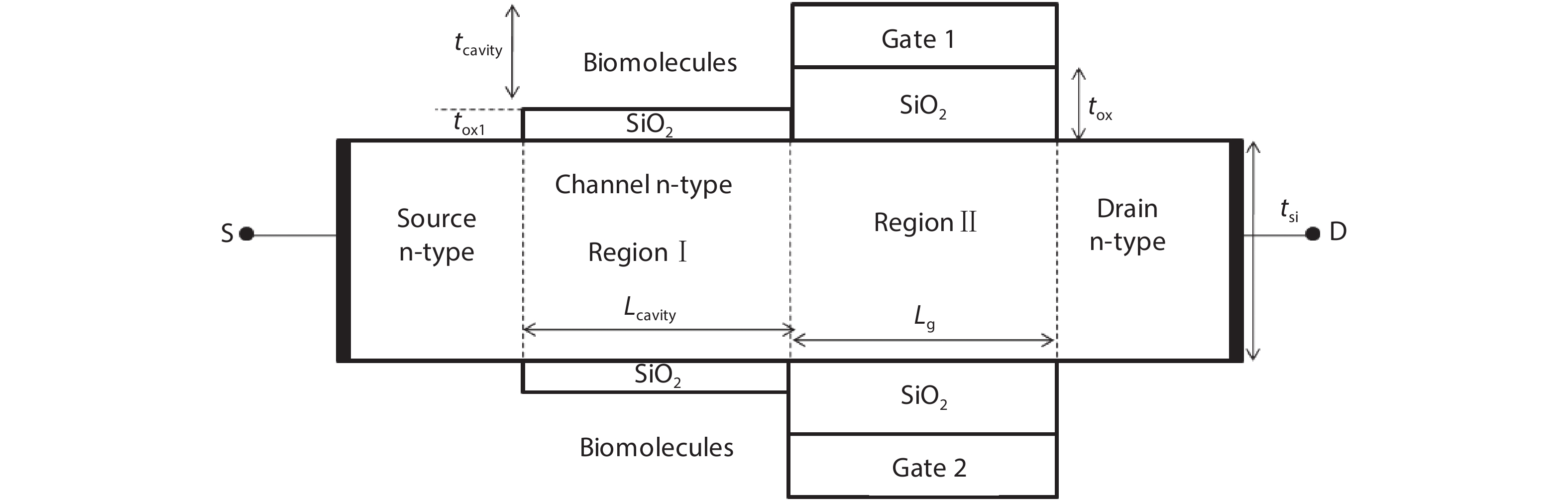
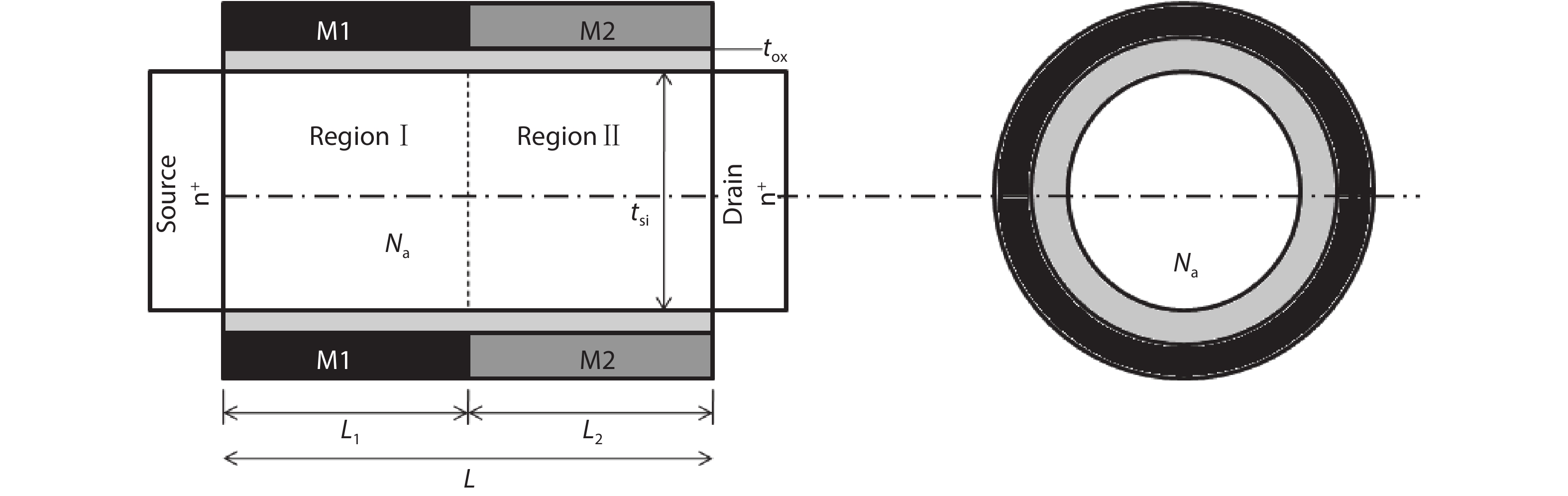
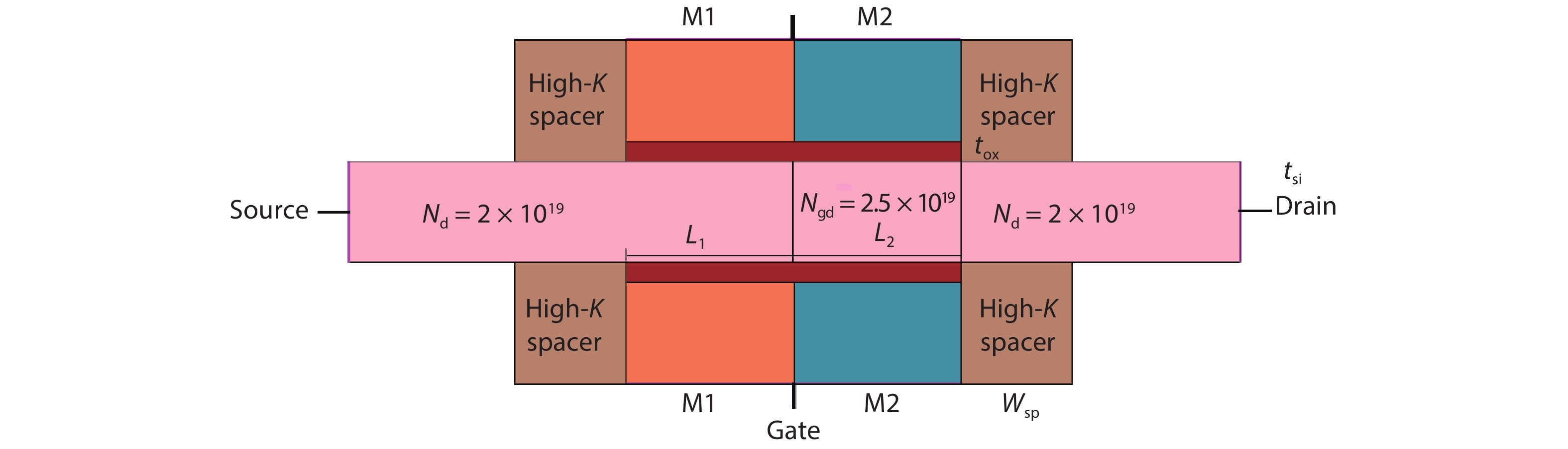
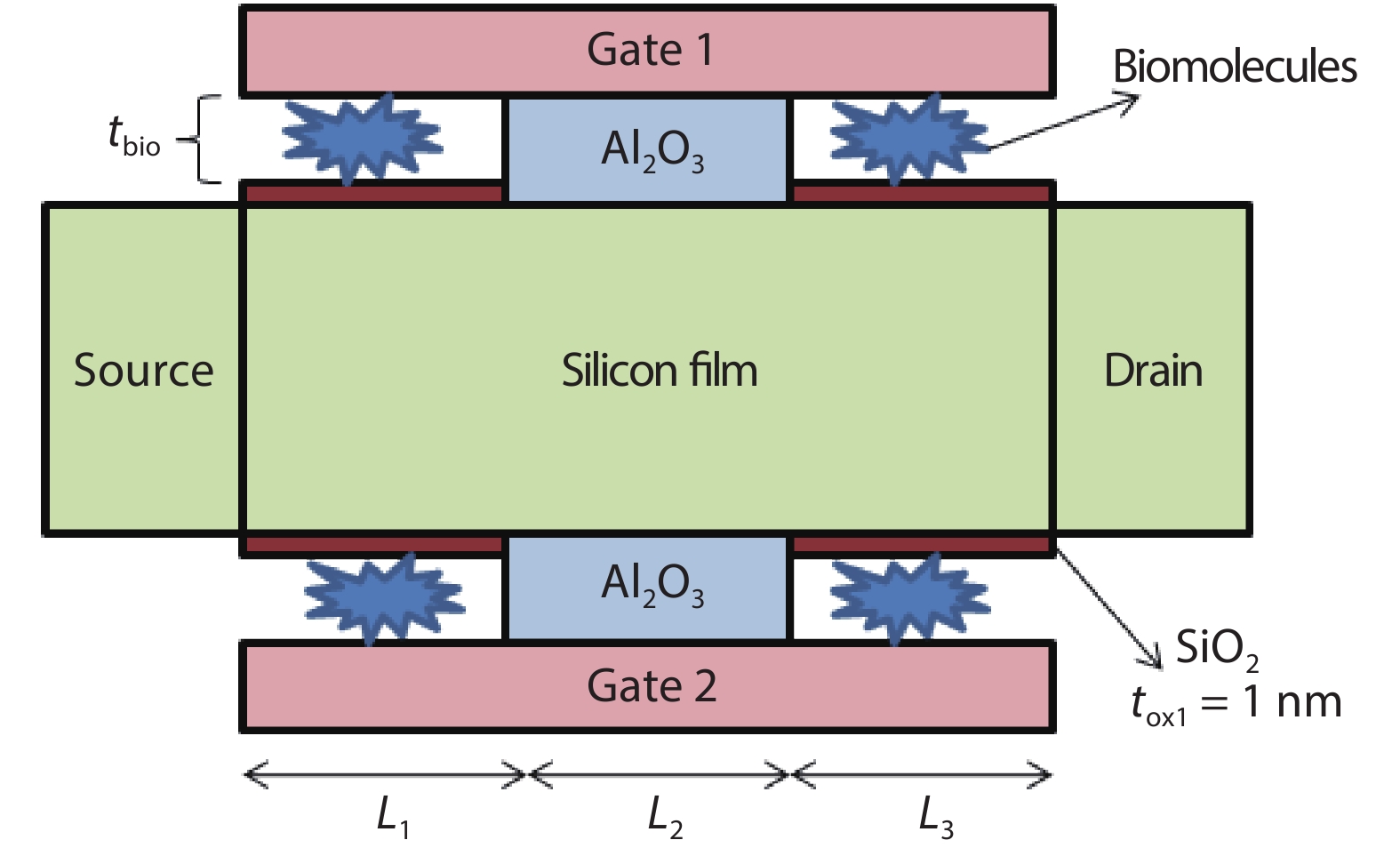
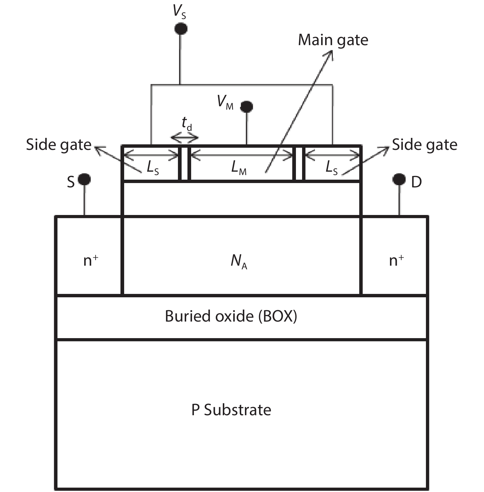
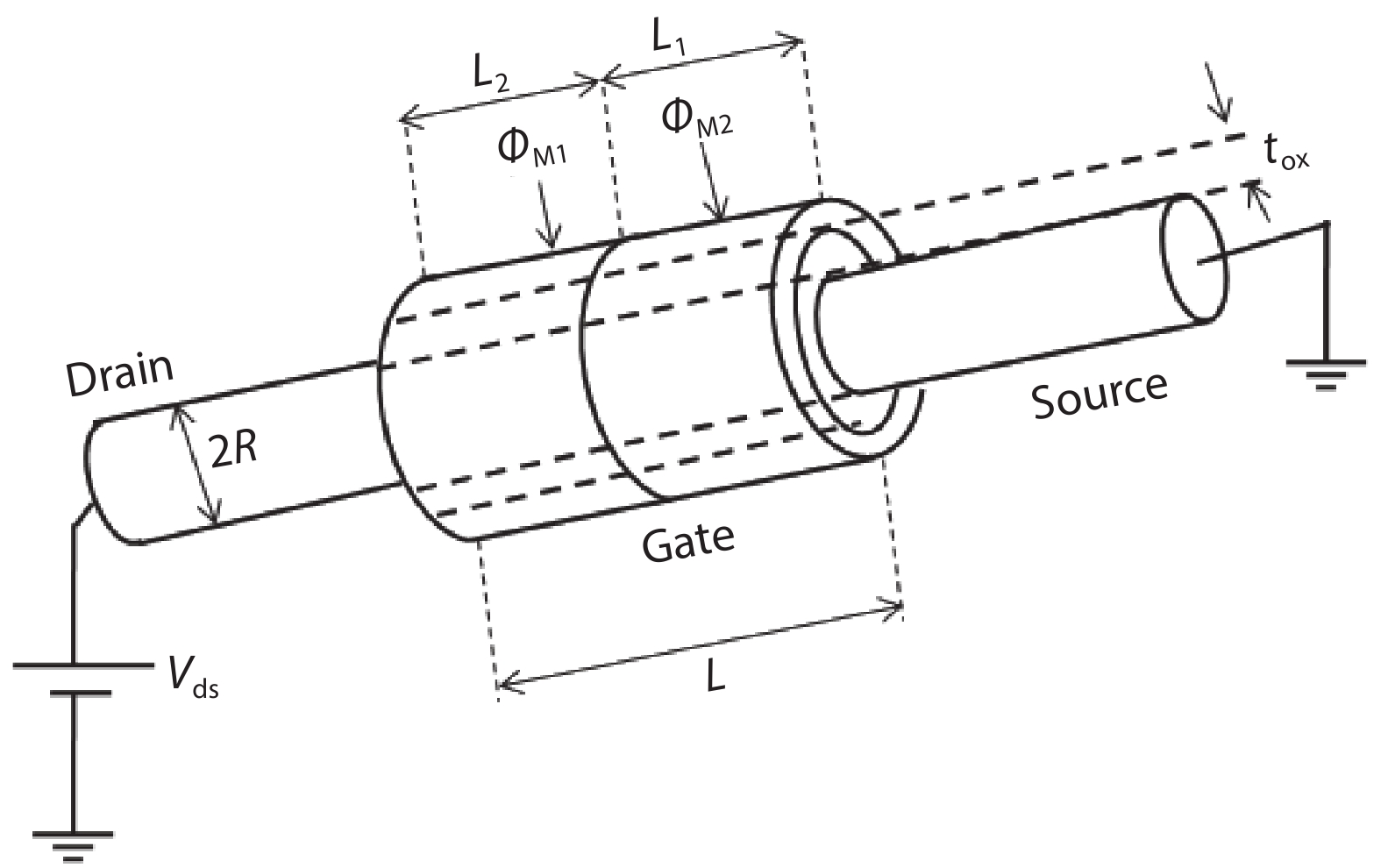
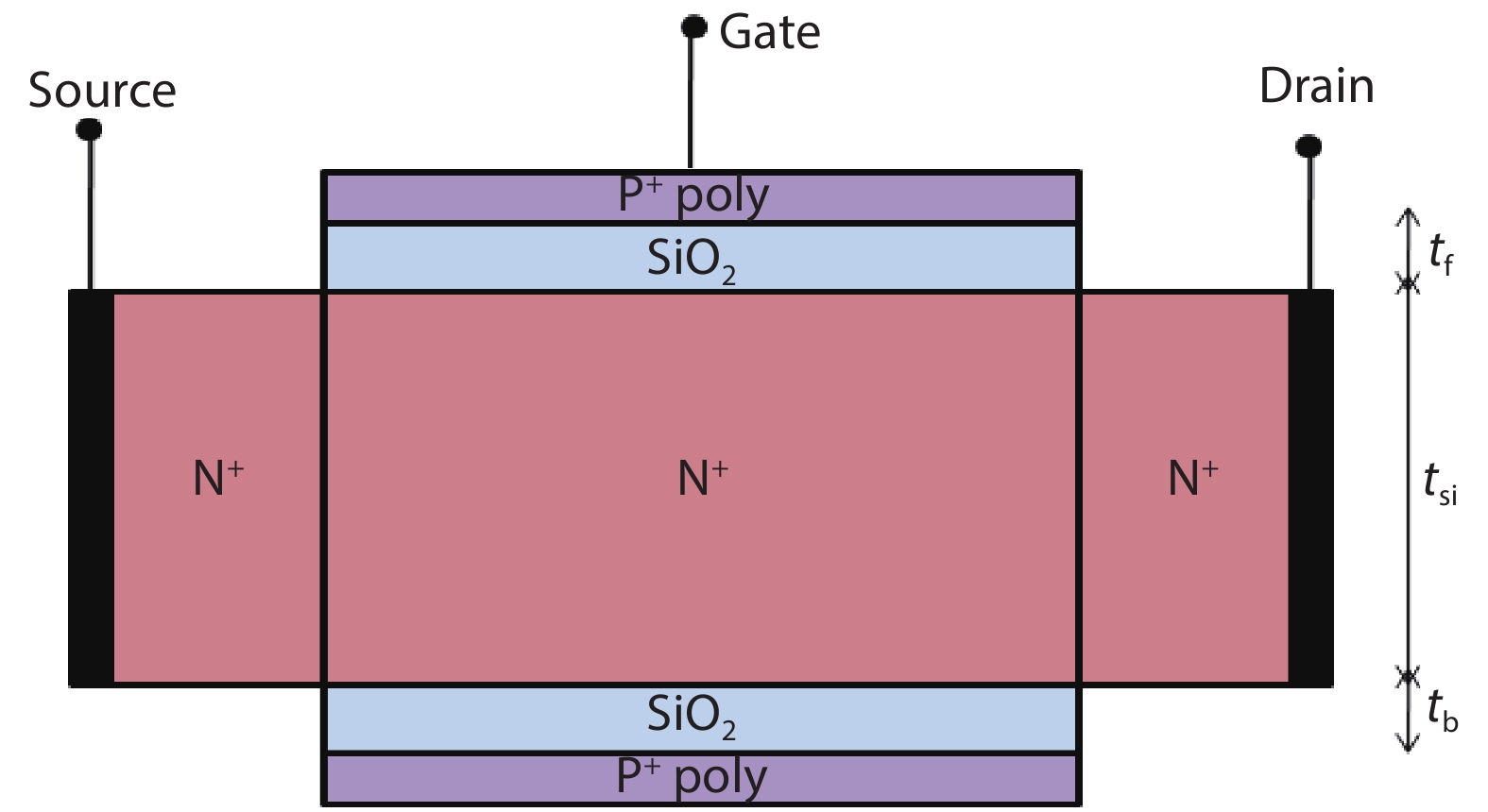
CMOS technology is one of the most frequently used technologies in the semiconductor industry as it can be successfully integrated with ICs. Every two years the number of MOS transistors doubles because the size of the MOSFET is reduced. Reducing the size of the MOSFET reduces the size of the channel length which causes short channel effects and it increases the leakage current. To reduce the short channel effects new designs and technologies are implemented. Double gate MOSFET design has shown improvement in performance as amplifiers over a single MOSFET. Silicon-based MOSFET design can be used in a harsh environment. It has been used in various applications such as in detecting biomolecules. The increase in number of gates increases the current drive capability of transistors. GAA MOSFET is an example of a quadruple gate around the four sides of channel that increases gate control over the channel region. It also increases effective channel width that improves drain current and reduces leakage current keeping short channel effects under limit. Junctionless MOSFET operates faster and uses less power with increase in ON-state current leading to a good value of ION/IOFF ratio. In this paper, several gate and channel engineered MOSFET structures are analyzed and compared for sub 45 nm technology node. A comparison among different MOSFET structures has been made for subthreshold performance parameters in terms of IOFF, subthreshold slope and DIBL values. The analog/RF performance is analyzed for transconductance, effective transistor capacitances, stability factor and critical frequency. The paper also covers different applications of advance MOSFET structures in analog/digital or IoT/ biomedical applications.


J. Semicond.
2020, 41(6): 062301 doi: 10.1088/1674-4926/41/6/062301
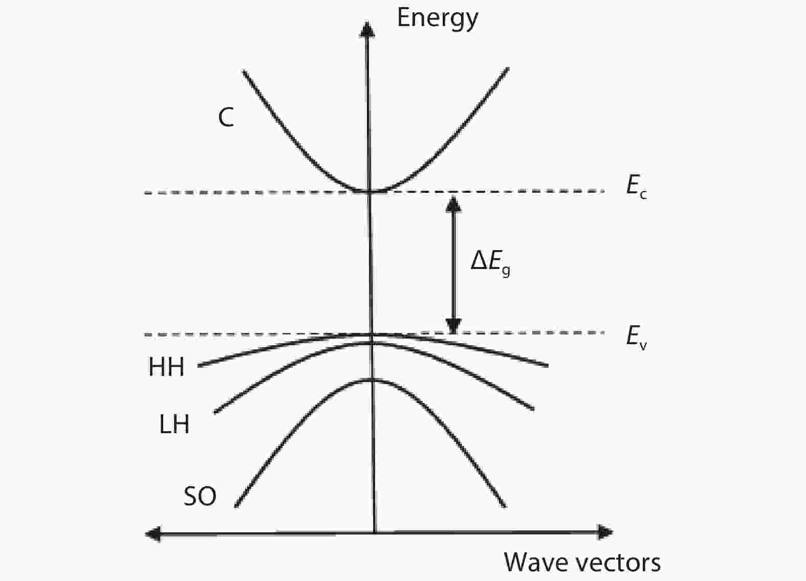
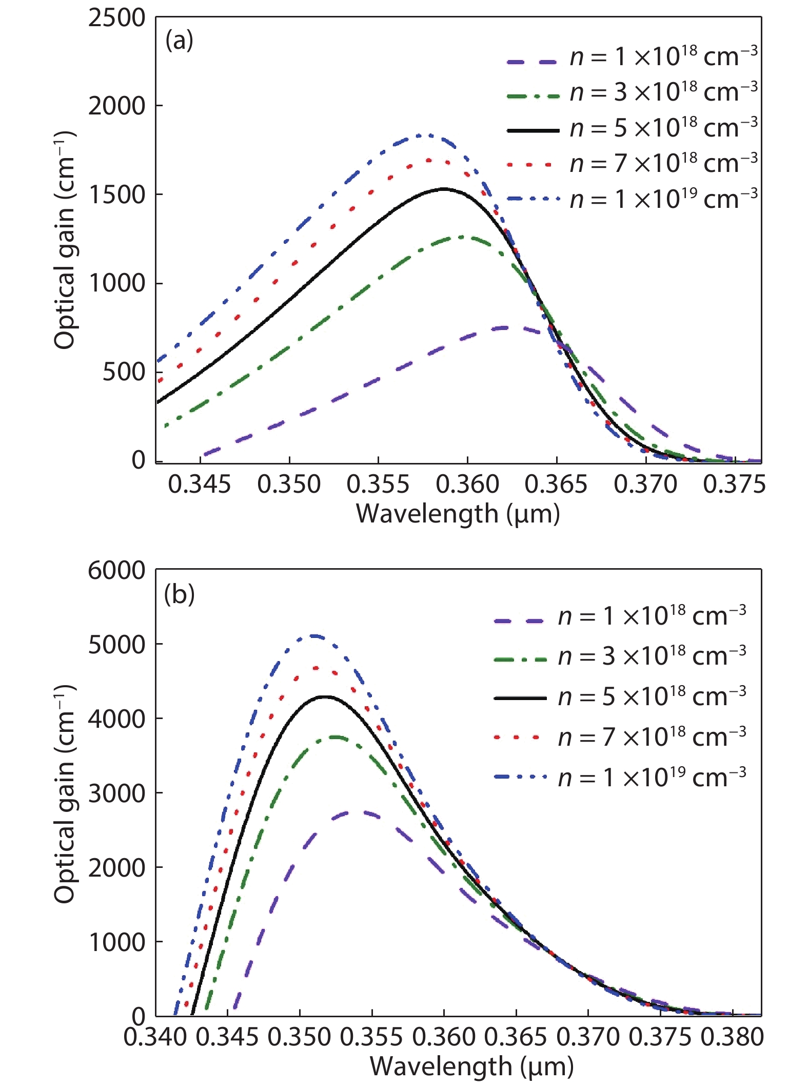
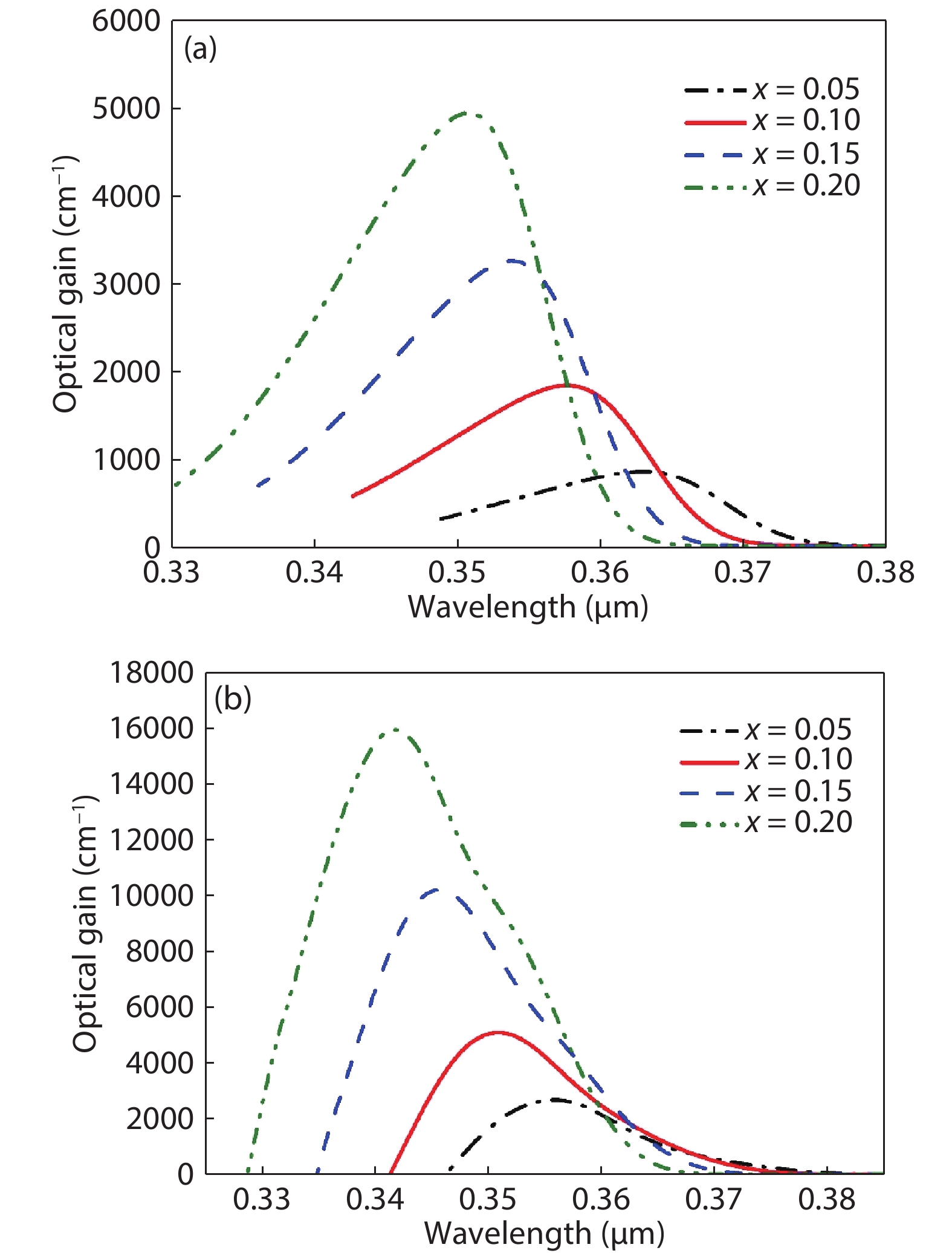
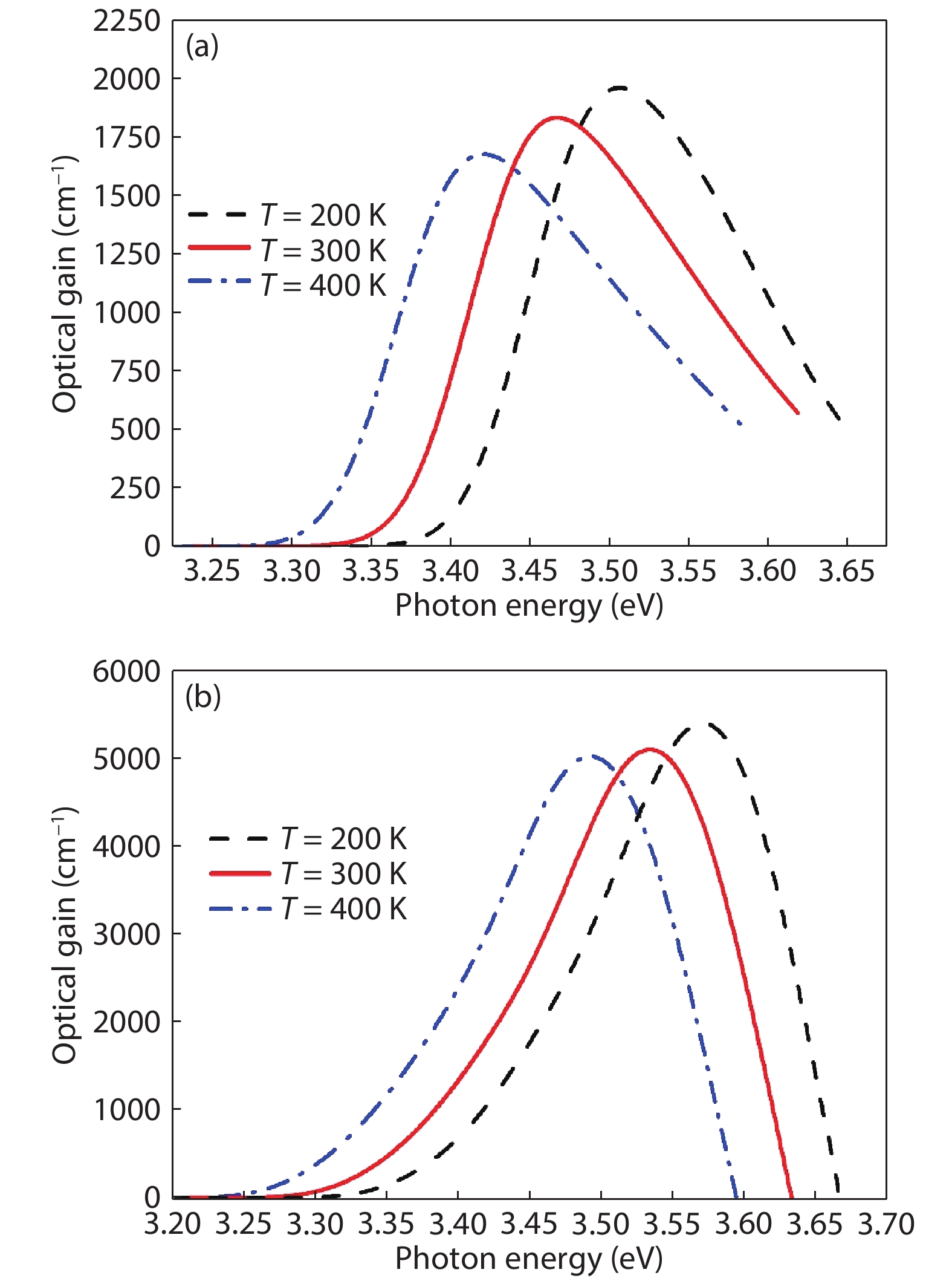
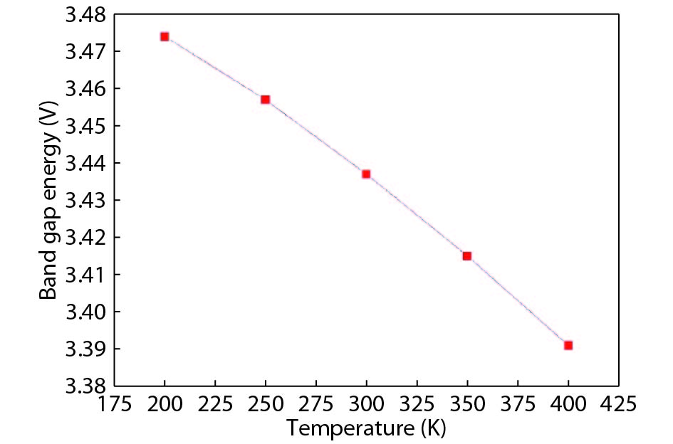
The effects of the quantum well (QW) width, carrier density, and aluminium (Al) concentration in the barrier layers on the optical characteristics of a gallium nitride (GaN)-based QW laser diode are investigated by means of a careful modelling analysis in a wide range of temperatures. The device’s optical gain is calculated by using two different band energy models. The first is based on the simple band-to-band model that accounts for carrier transitions between the first levels of the conduction band and valence band, whereas the second assumes the perturbation theory (k.p model) for considering the valence intersubband transitions and the relative absorption losses in the QW. The results reveal that the optical gain increases with increasing the n-type doping density as well as the Al molar fraction of the AlxGa1–xN layers, which originate the GaN compressive-strained QW. In particular, a significant optical gain on the order of 5000 cm–1 is calculated for a QW width of 40 Å at room temperature. In addition, the laser threshold current density is of few tens of A/cm2 at low temperatures.


J. Semicond.
2020, 41(6): 062302 doi: 10.1088/1674-4926/41/6/062302

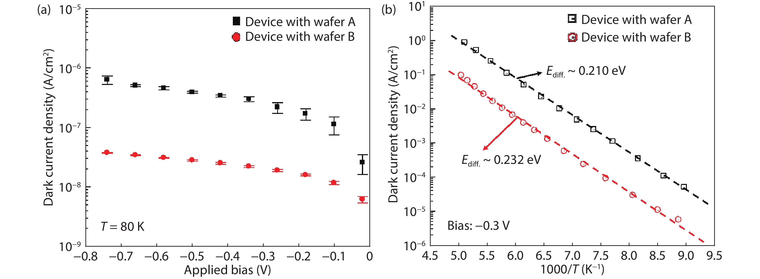
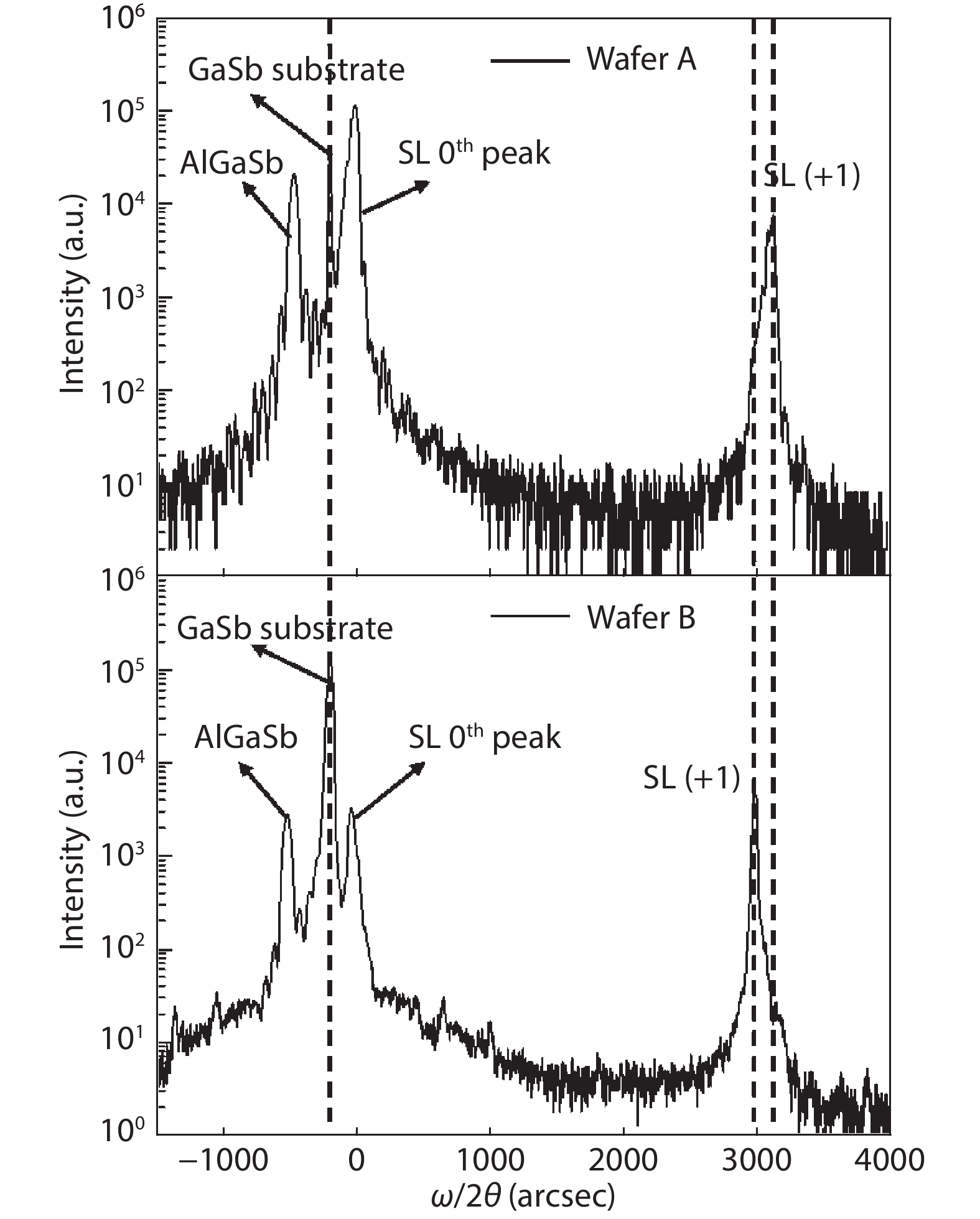
Type-II superlattice (T2SL) materials are the key element for infrared (IR) detectors. However, it is well known that the characteristics of the detectors with the T2SL layer are greatly affected by the strain developed during the growth process, which determines the performance of IR detectors. Therefore, great efforts have been made to properly control the strain effect and develop relevant analysis methods to evaluate the strain-induced dark current characteristics. In this work, we report the strain-induced dark current characteristics in InAs/GaSb T2SL MWIR photodetector. The overall strain of InAs/GaSb T2SL layer was analyzed by both high-resolution X-ray diffraction (HRXRD) and the dark current measured from the absorber layer at the elevated temperatures (≥ 110 K), where the major leakage current component is originated from the reduced minority carrier lifetime in the absorber layer. Our findings indicate that minority carrier lifetime increases as the tensile strain on the InAs/GaSb T2SL is more compensated by the compressive strain through ‘InSb-like’ interface, which reduces the dark current density of the device. Specifically, tensile strain compensated devices exhibited the dark current density of less than 2 ×10⁻⁵ A/cm2 at 120 K, which is more than one order of magnitude lower value compared to that of the device without tensile strain relaxation.


J. Semicond.
2020, 41(6): 062303 doi: 10.1088/1674-4926/41/6/062303
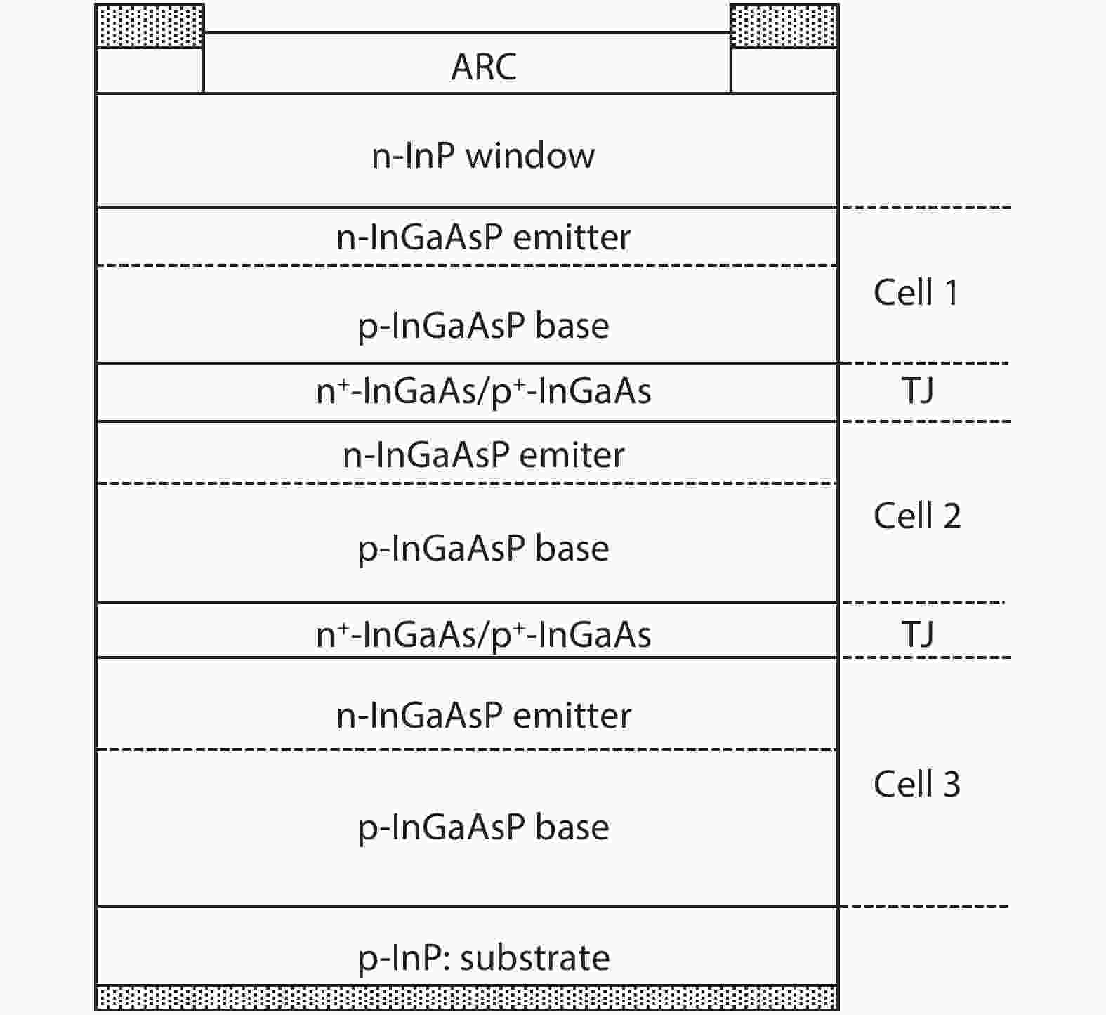
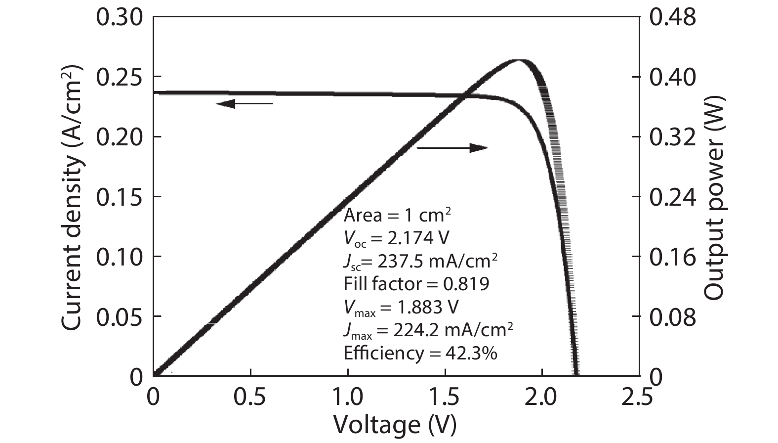
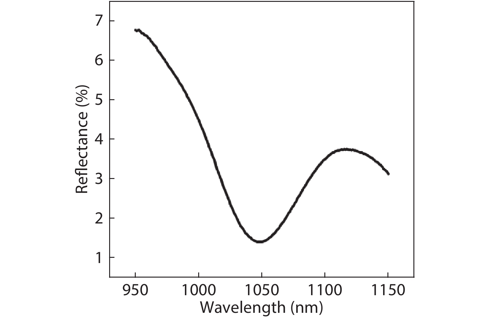
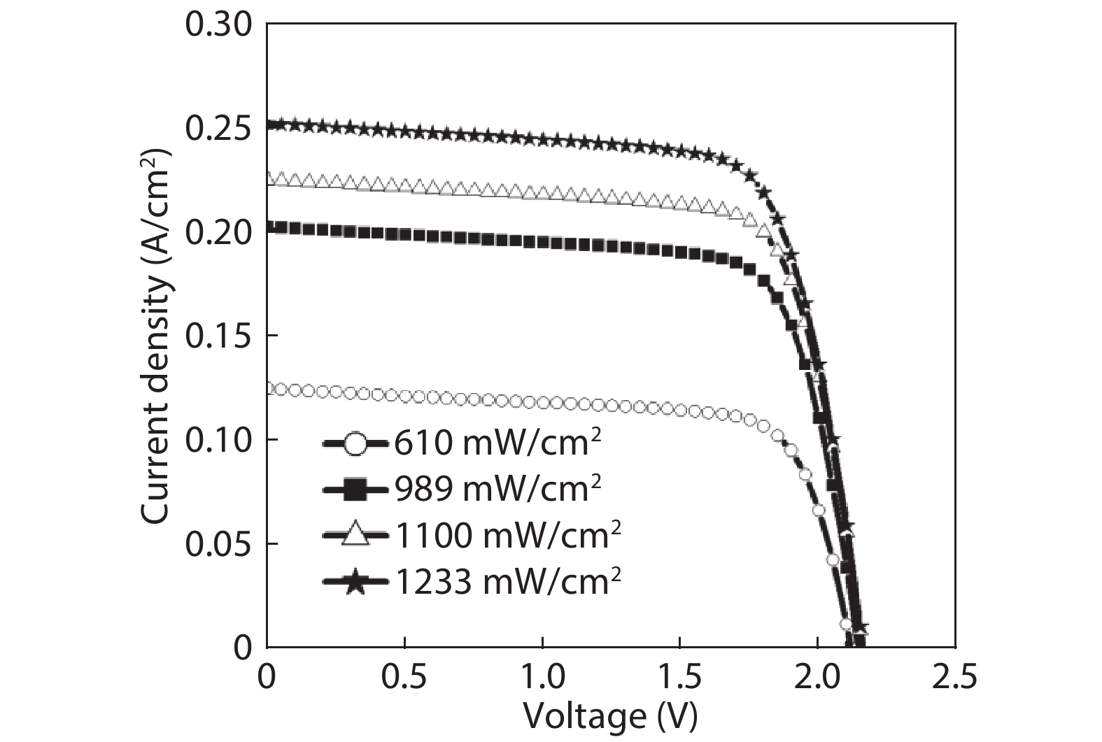
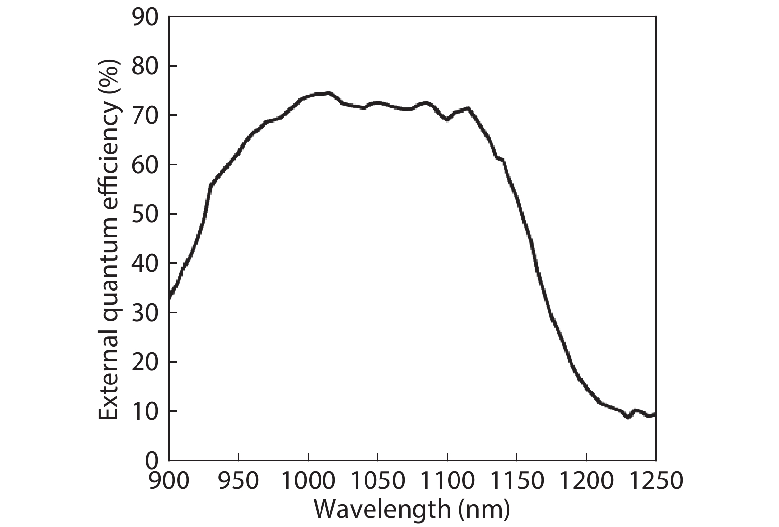
Laser photovoltaic devices converting 1064 nm light energy into electric energy present a promising prospect in wireless energy transmission due to the commercial availability of high power 1064 nm lasers with very small divergence. Besides their high conversion efficiency, a high output voltage is also expected in a laser energy transmission system. Meanwhile, 1064 nm InGaAsP multi-junction laser power converters have been developed using p+-InGaAs/n+-InGaAs tunnel junctions to connect sub-cells in series to obtain a high output voltage. The triple-junction laser power converter structures are grown on p-type InP substrates by metal-organic chemical vapor deposition (MOCVD), and InGaAsP laser power converters are fabricated by conventional photovoltaic device processing. The room-temperature I–V measurements show that the 1 × 1 cm2 triple-junction InGaAsP laser power converters demonstrate a conversion efficiency of 32.6% at a power density of 1.1 W/cm2, with an open-circuit voltage of 2.16 V and a fill factor of 0.74. In this paper, the characteristics of the laser power converters are analyzed and ways to improve the conversion efficiency are discussed.

J. Semicond.
2020, 41(6): 062401 doi: 10.1088/1674-4926/41/6/062401

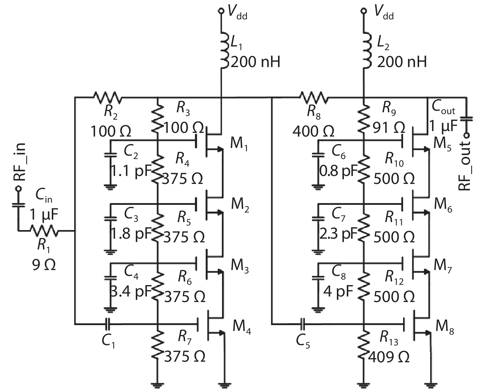
In this letter, we design and analyze 0.1–1.5 GHz multi-octave quadruple-stacked CMOS power amplifier (PA) in 0.18 μm CMOS technology. By using two-stage quadruple-stacked topology and feedback technology, the proposed PA realizes an ultra-wideband CMOS PA in a small chip area. Wideband impedance matching is achieved with smaller chip dimension. The effects of feedback resistors on the RF performance are also discussed for this stacked-FET PA. The PA shows measured input return loss (< –10.8 dB) and output return loss (< –9.6 dB) in the entire bandwidth. A saturated output power of 22 dBm with maximum 20% power added efficiency (PAE) is also measured with the drain voltage at 5 V. The chip size is 0.44 mm2 including all pads.


J. Semicond.
2020, 41(6): 062402 doi: 10.1088/1674-4926/41/6/062402
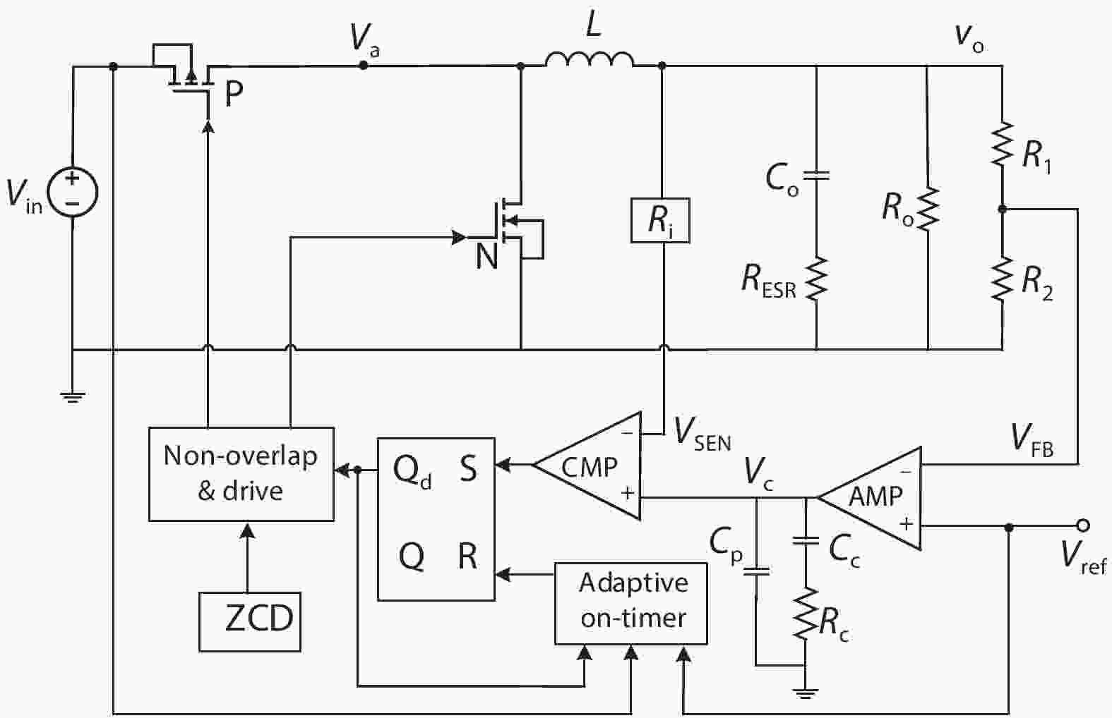
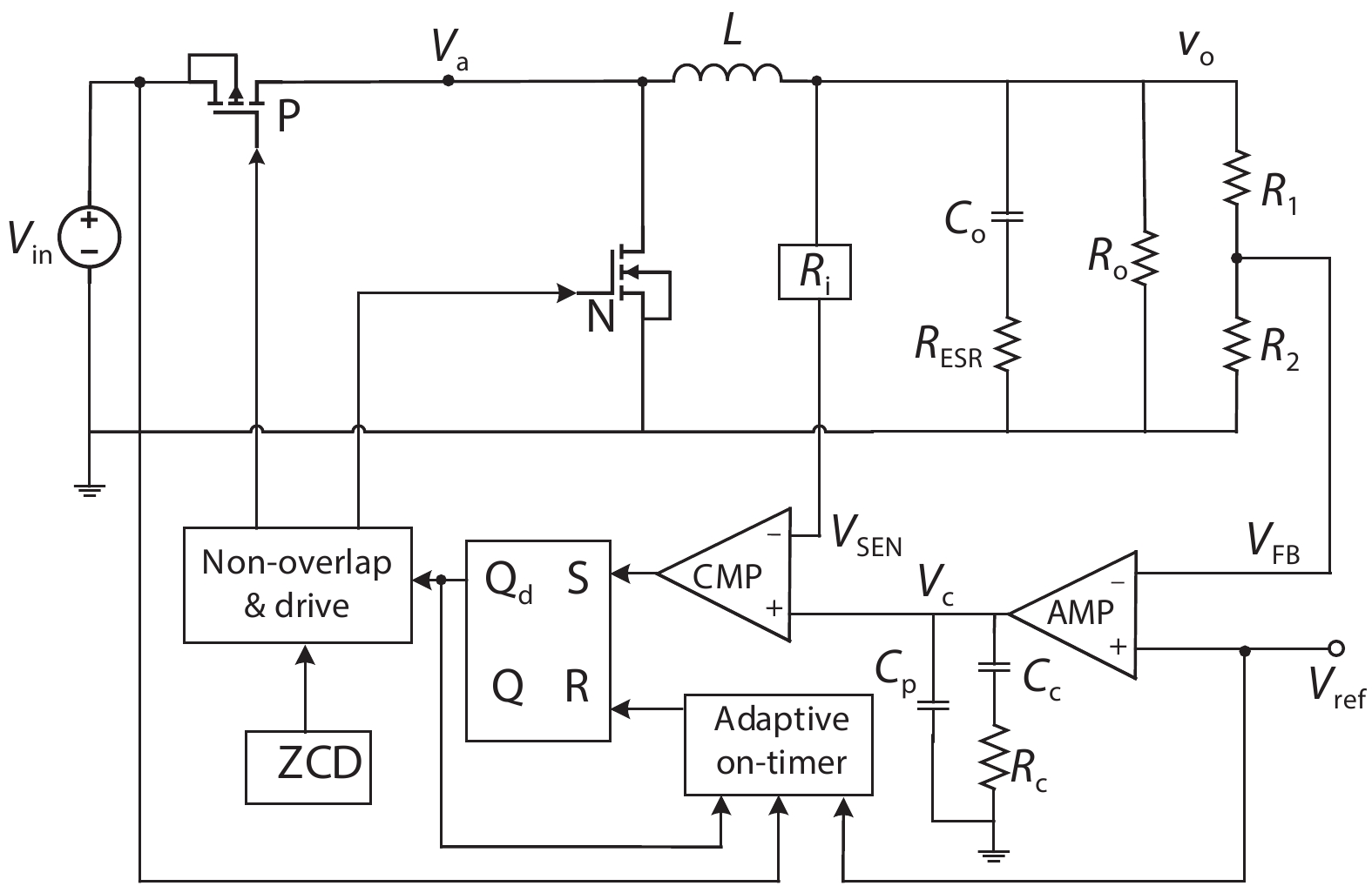
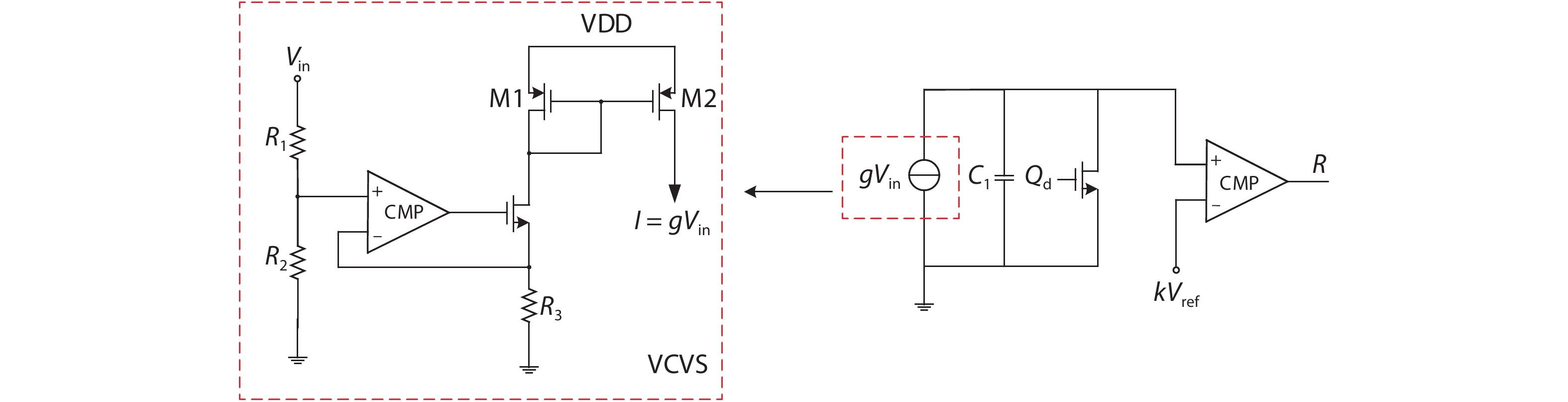
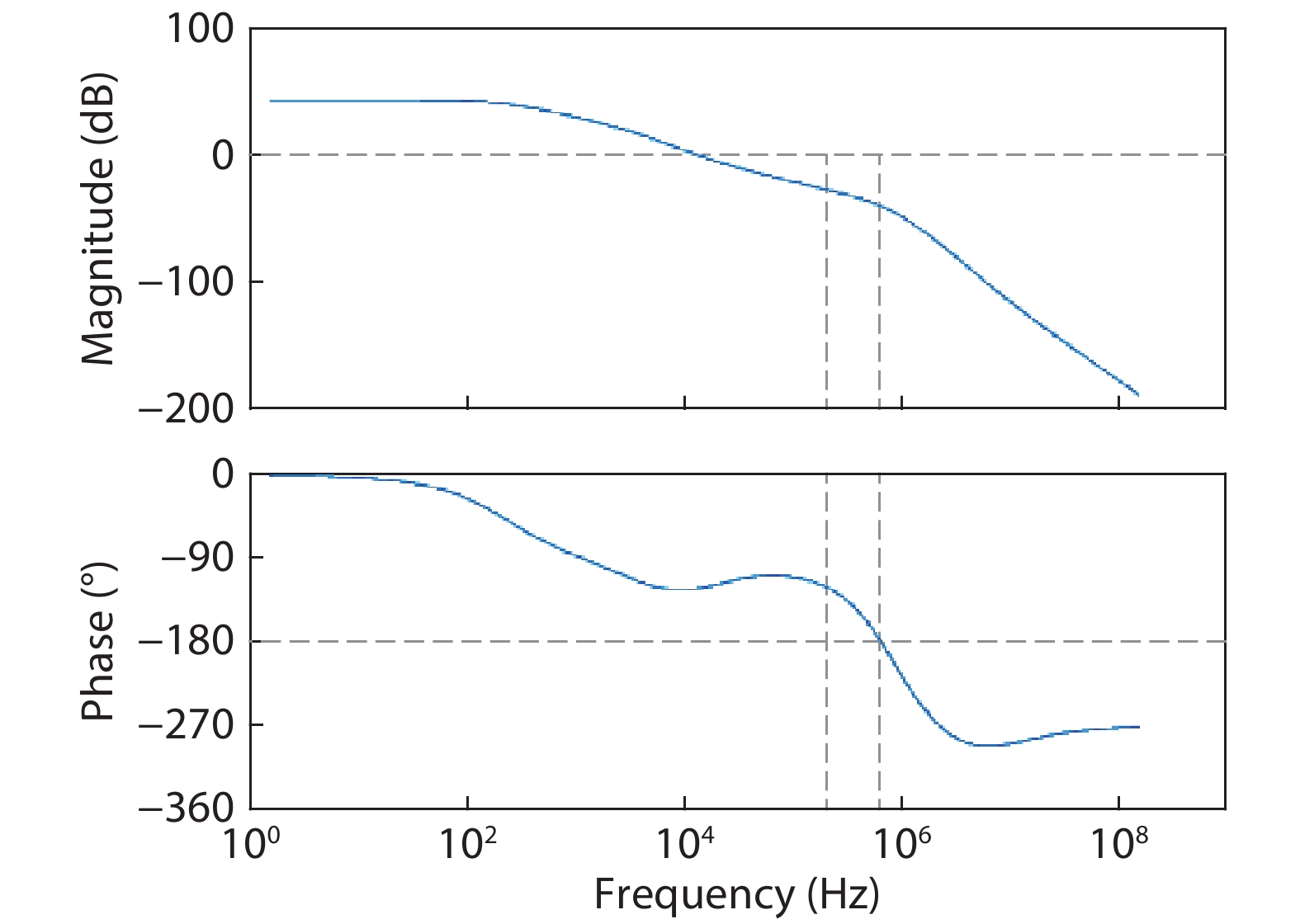
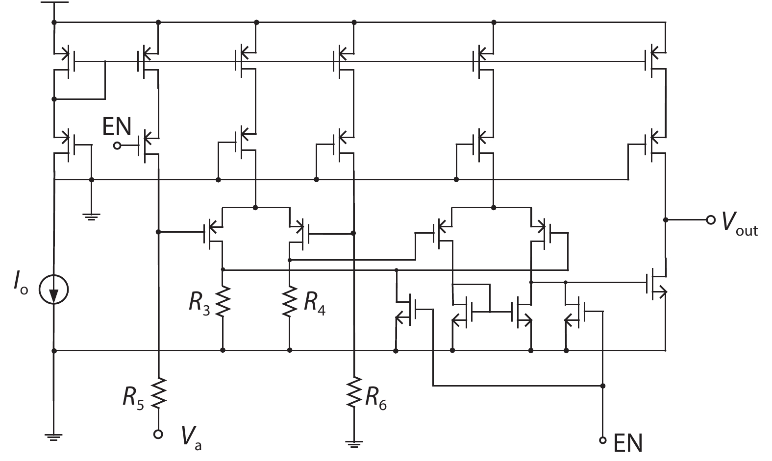
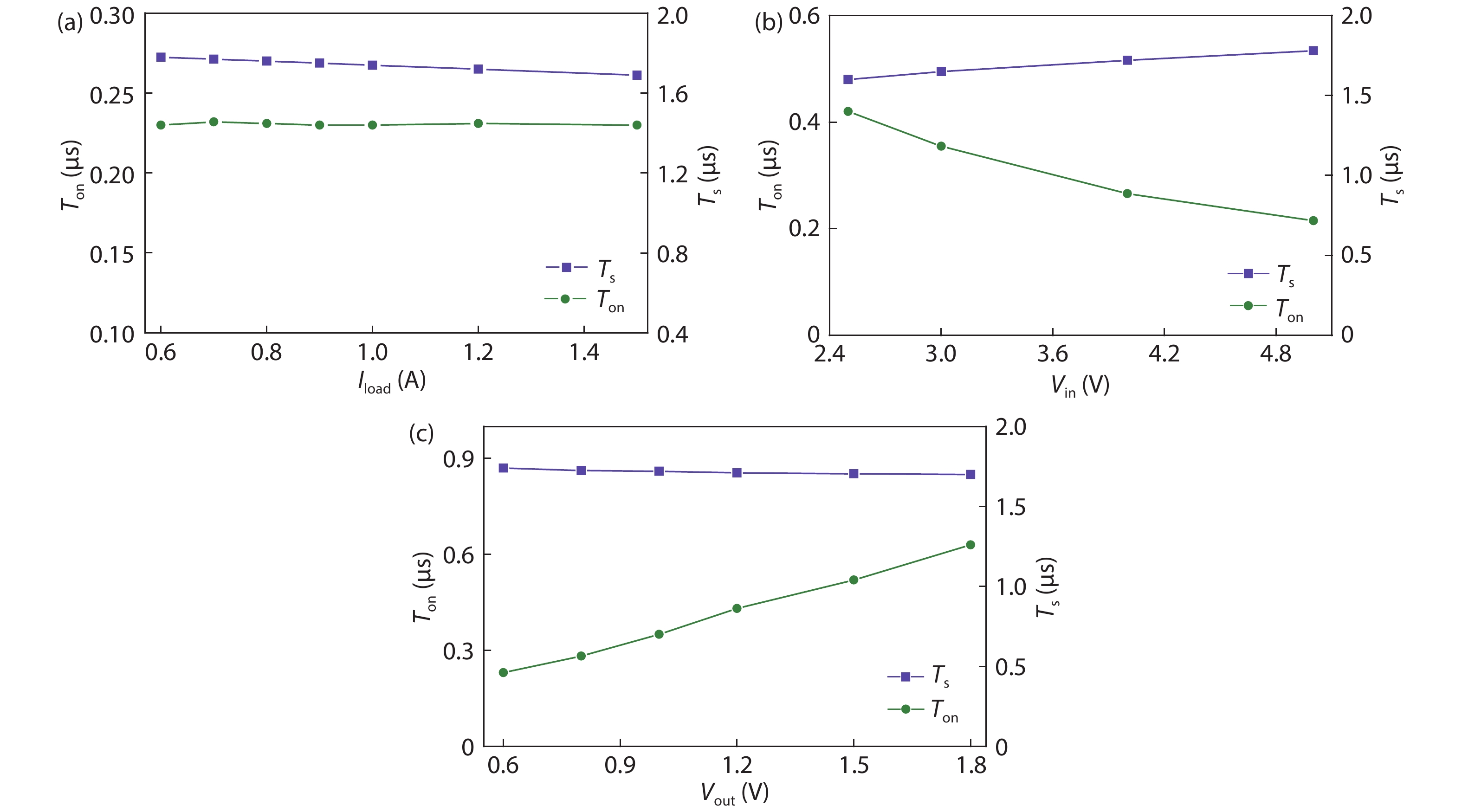
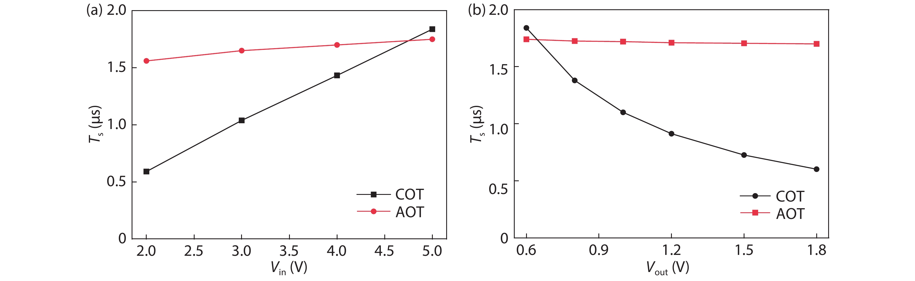
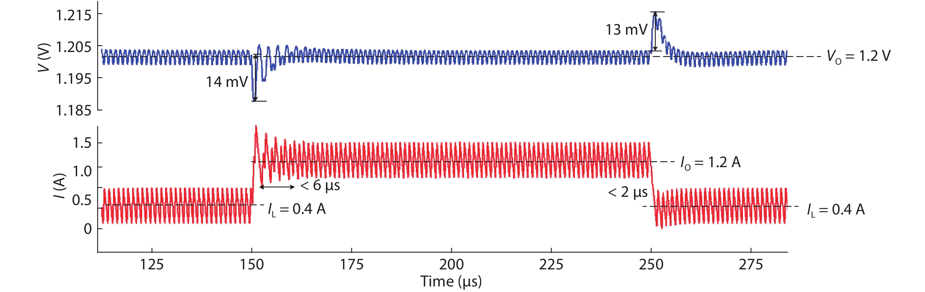
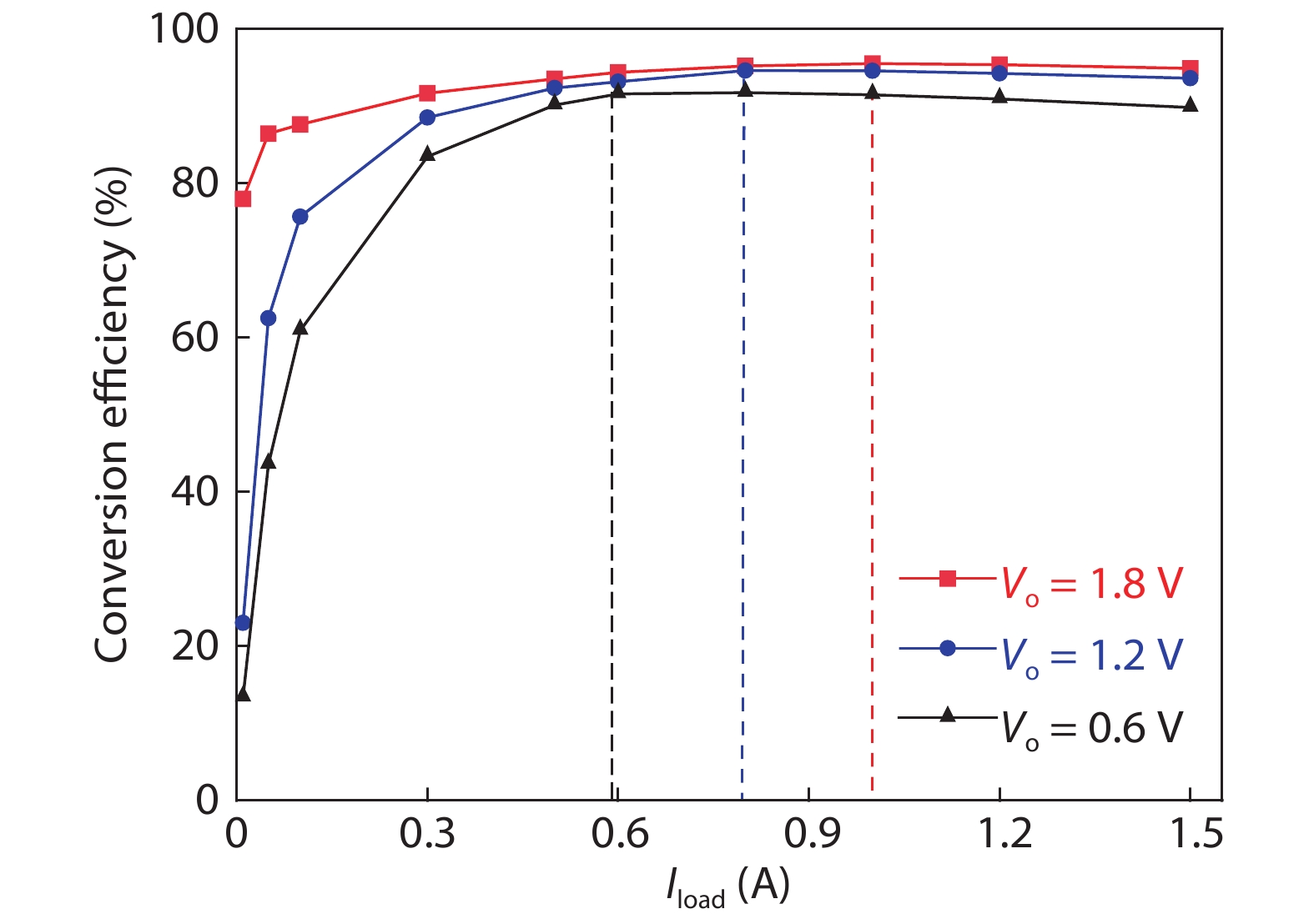
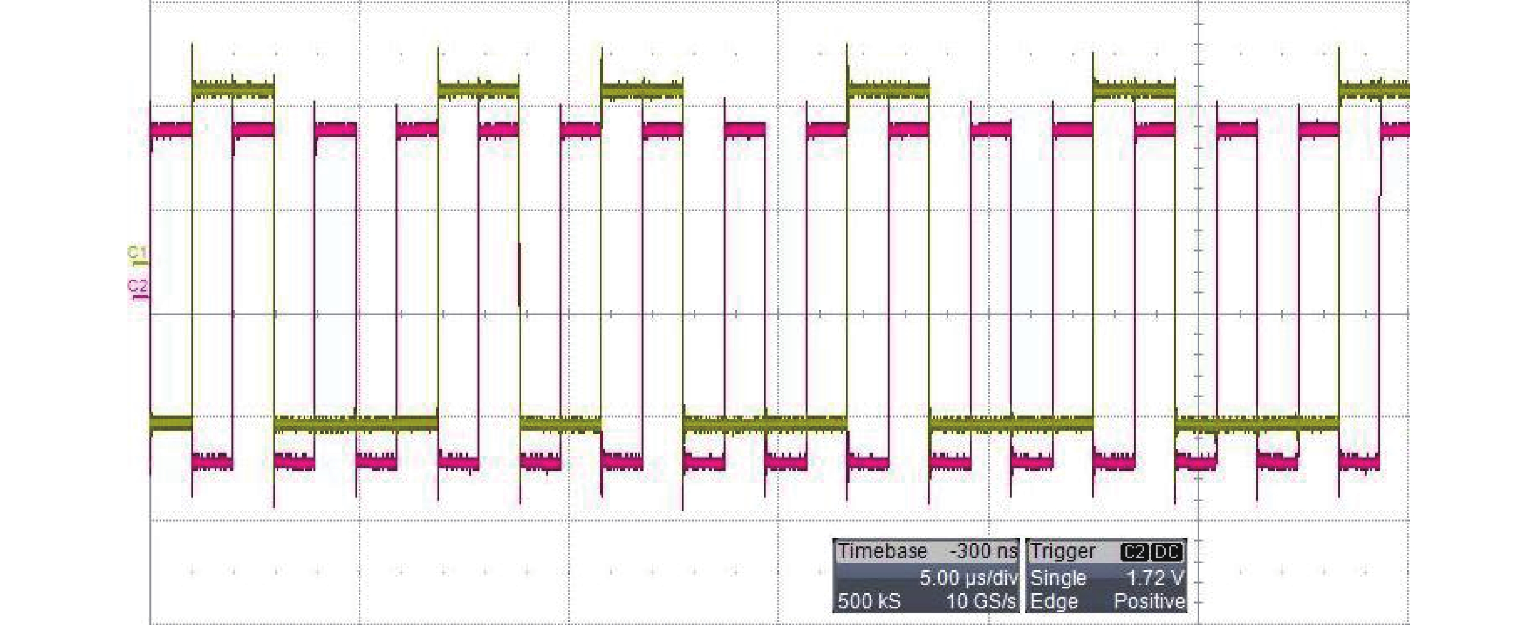
This paper presents an AOT-controlled (adaptive-on-time, AOT) valley-current-mode buck converter for portable application. The buck converter with synchronous rectifier not only uses valley-current-mode control but also possesses hybrid-mode control functions at the same time. Due to the presence of the zero-current detection circuit, the converter can switch freely between the two operating modes without the need for an external mode selection circuit, which further reduces the design difficulty and chip area. The converter for the application of high power efficiency and wide current range is used to generate the voltage of 0.6–3.0 V with a battery source of 3.3–5.0 V, while the load current range is 0.05–2 A. The circuit can work in continuous conduction mode with constant frequency in high load current range. In addition, a stable output voltage can be obtained with small voltage ripple. In pace with the load current decreases to a critical value, the converter transforms into the discontinuous conduction mode smoothly. As the switching period increases, the switching loss decreases, which can significantly improve the conversion efficiency. The proposed AOT controlled valley current mode buck converter is integrated with standard 0.18 μm process and the simulation results show that the converter provides well-loaded regulations with power efficiency over 95%. When the circuit switches between the two conduction modes drastically, the response time can be controlled within 30 μs. The undershoot voltage is controlled within 25 mV under a large current hopping range.


J. Semicond.
2020, 41(6): 062403 doi: 10.1088/1674-4926/41/6/062403
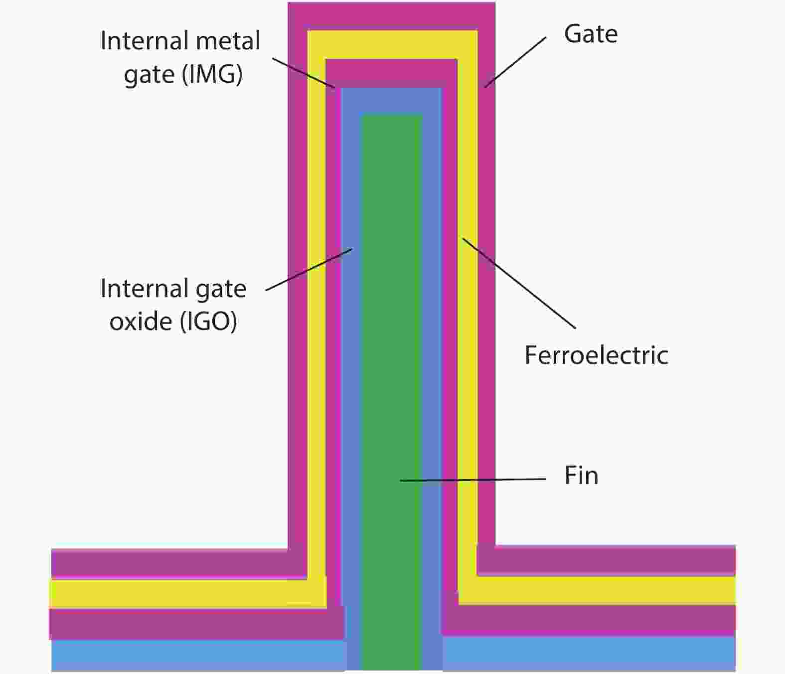
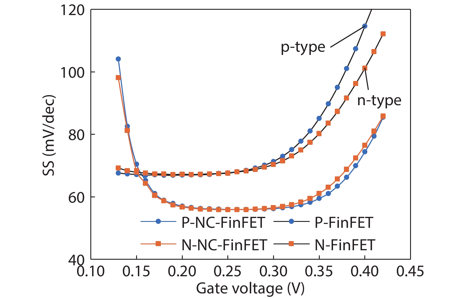
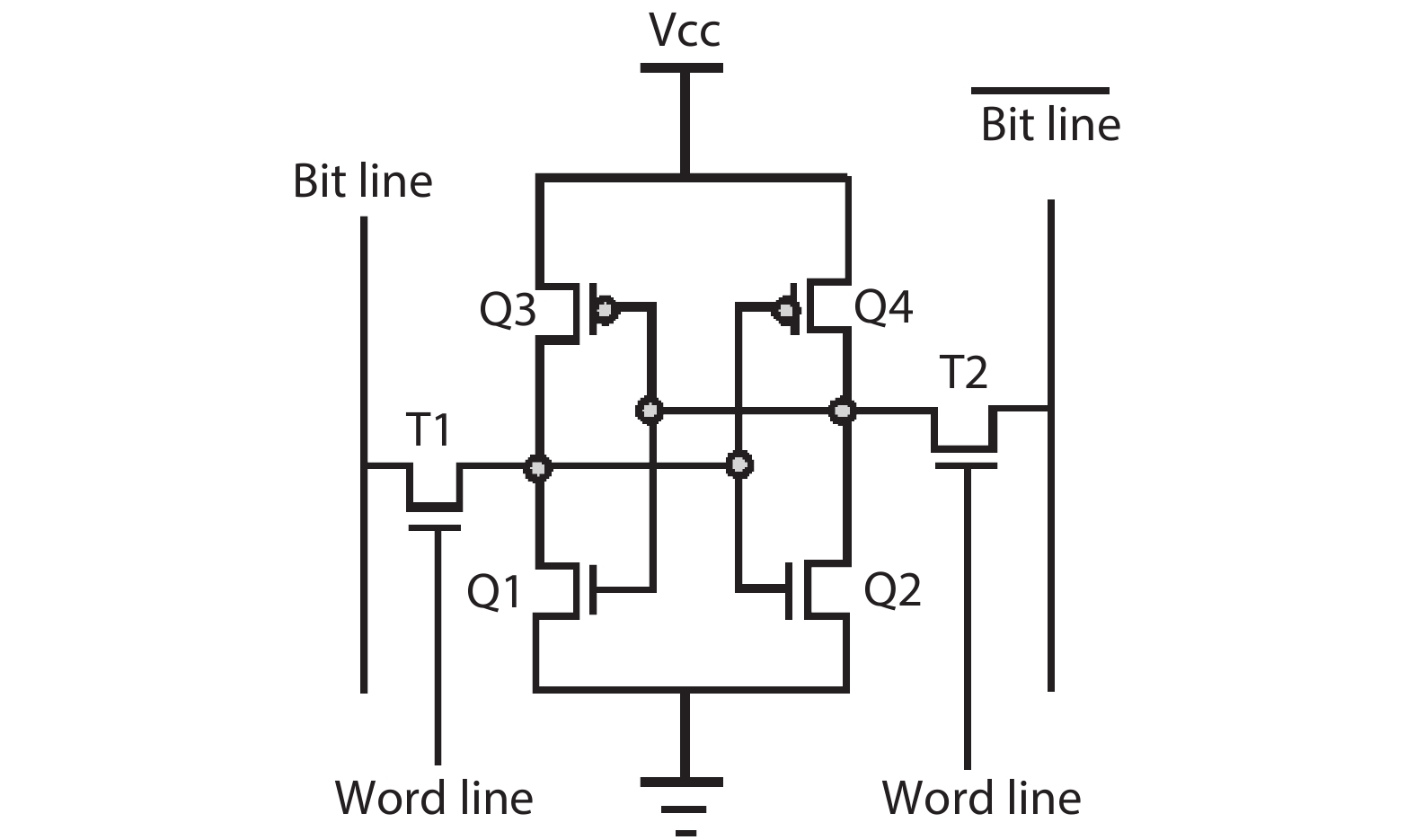
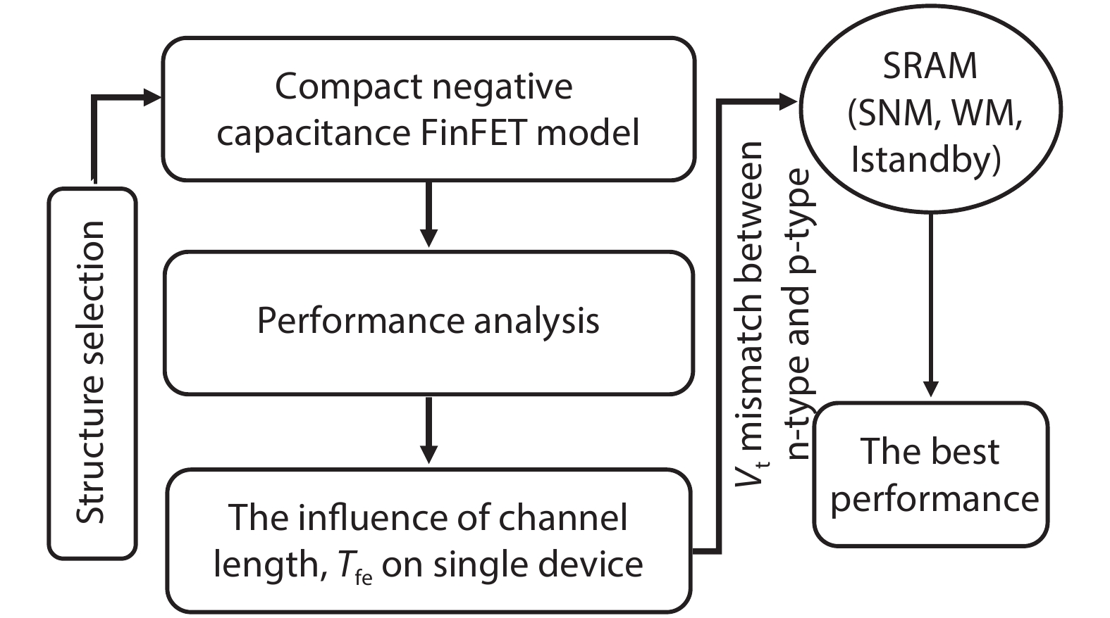
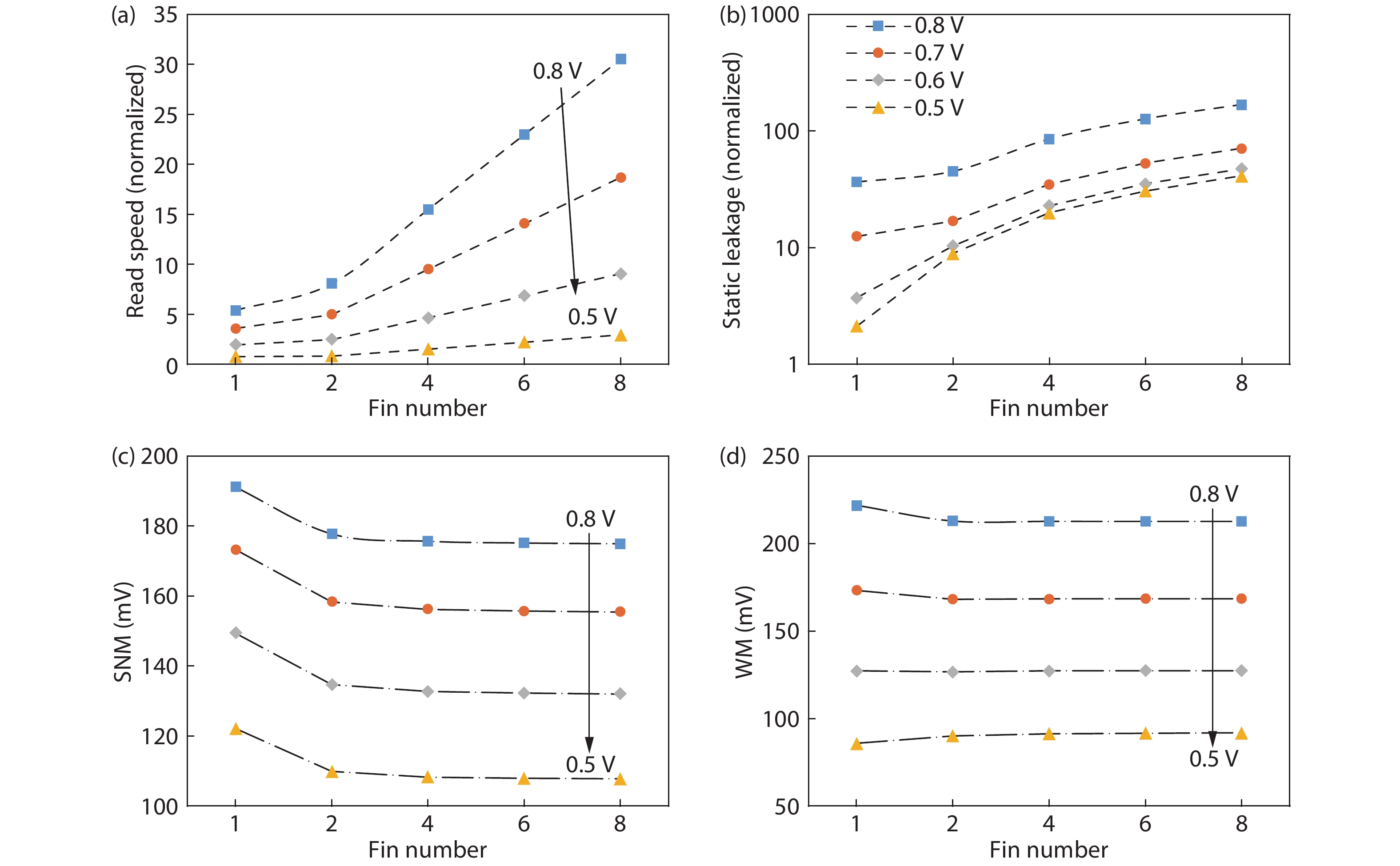
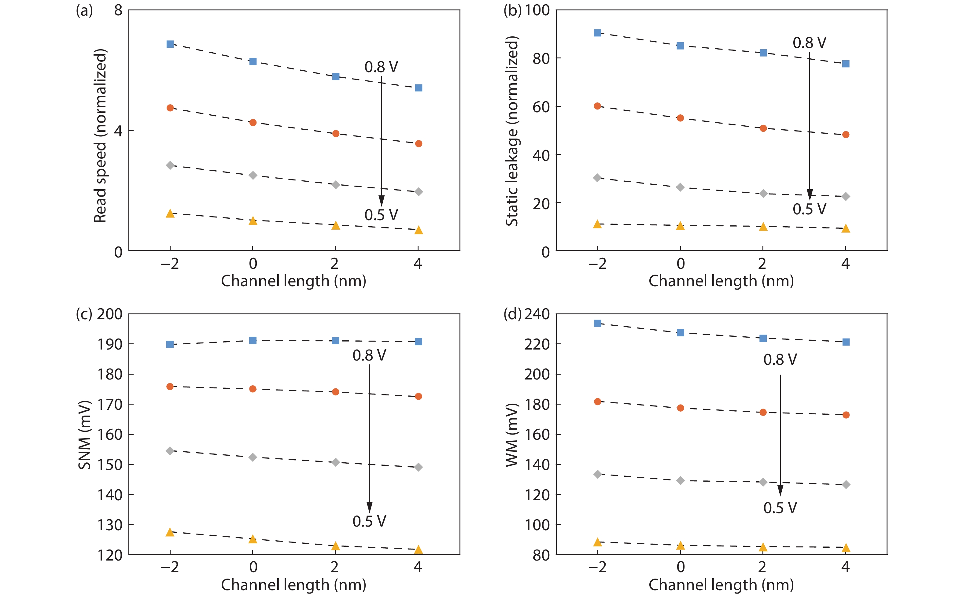
Negative capacitance FinFET (NC-FinFET) has a promising developmental prospect due to its superior performance in SS < 60 mV/dec (subthreshold swing), especially in SRAM. Noise margin is an important metric to evaluate the performance for SRAM, together with static leakage, read speed, etc. In this paper, we study the effects of the variation of ferroelectric material (thickness, polarization), FinFET critical physical parameters (fin number, channel length) and some ambient factors (working temperature, supply voltage) on the performance of NC-FinFET SRAM within the reasonable fluctuation tolerance range. The SRAM bit cell is analyzed with a basic 6T structure. The impact of fin number and channel length for NC-FinFET SRAM is different from that of conventional FinFETs. Additionally, the ferroelectric material and some other factors are assessed in detail.


J. Semicond.
2020, 41(6): 062404 doi: 10.1088/1674-4926/41/6/062404
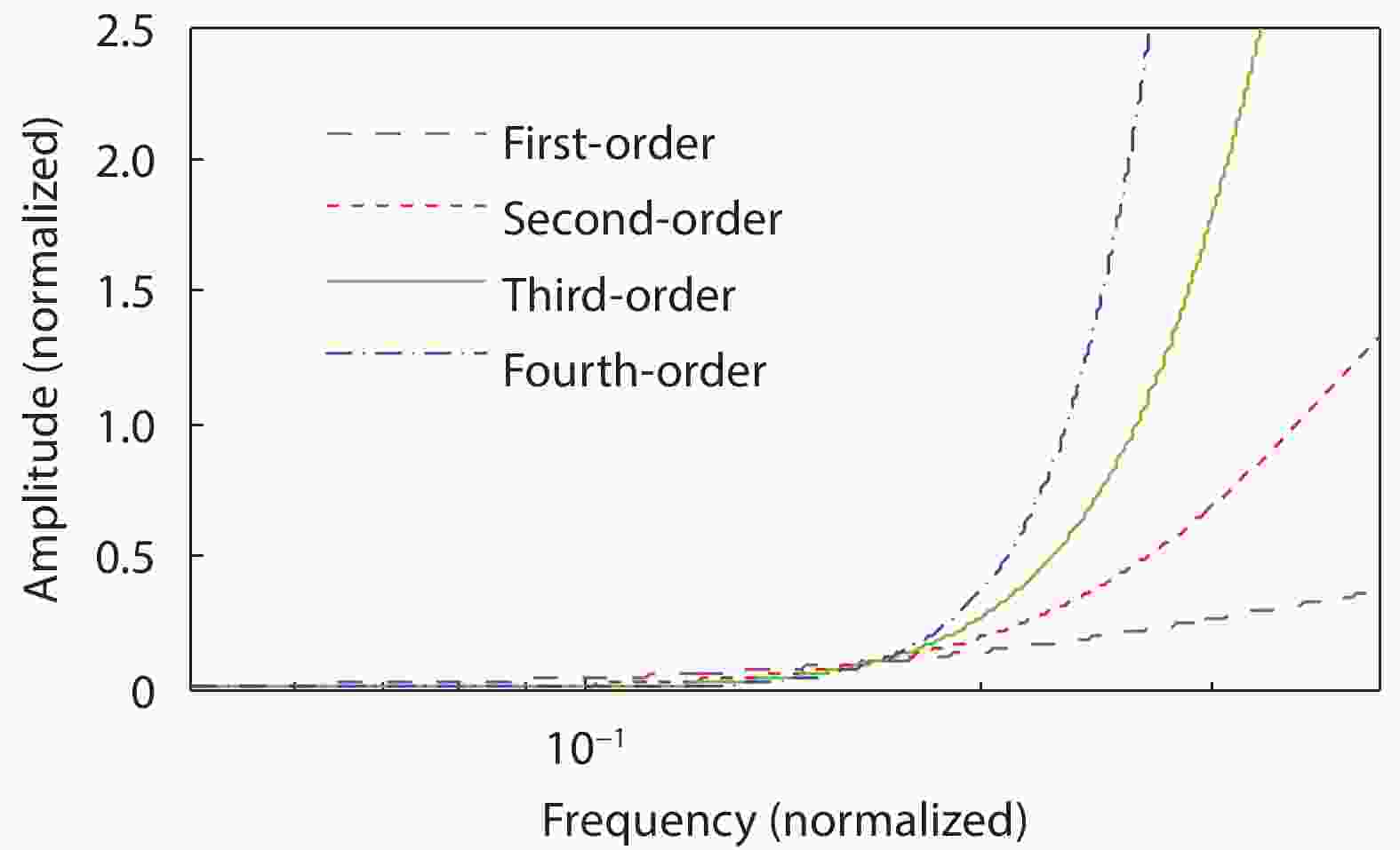
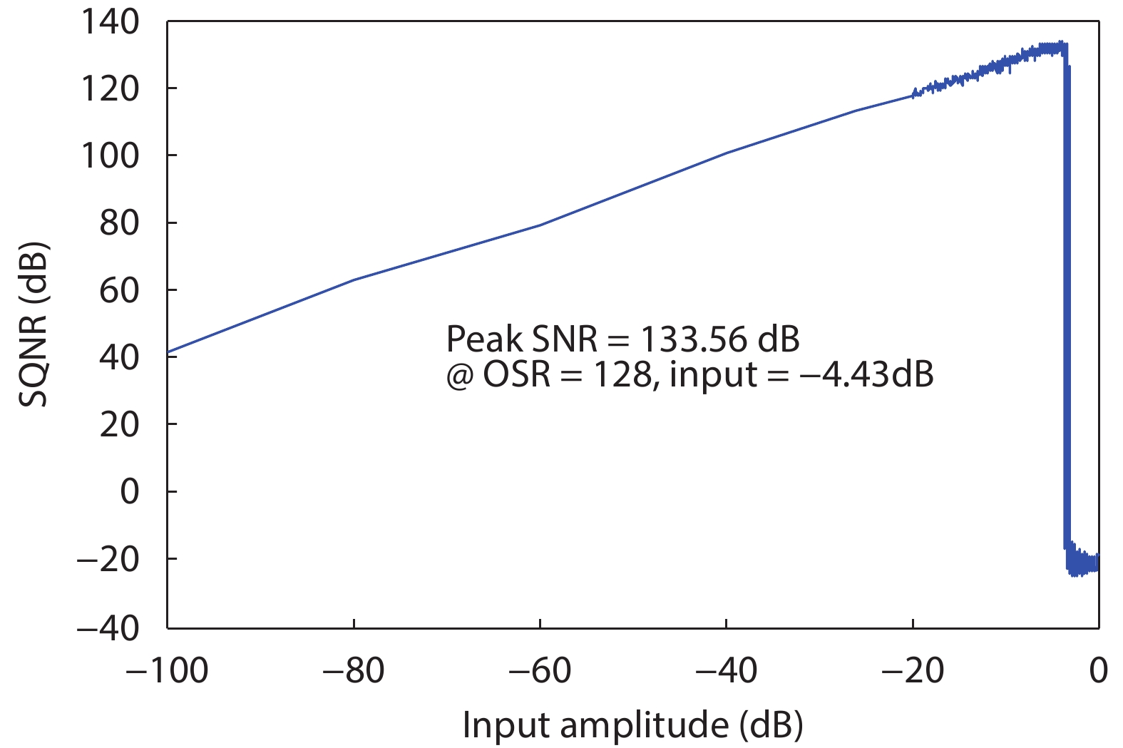
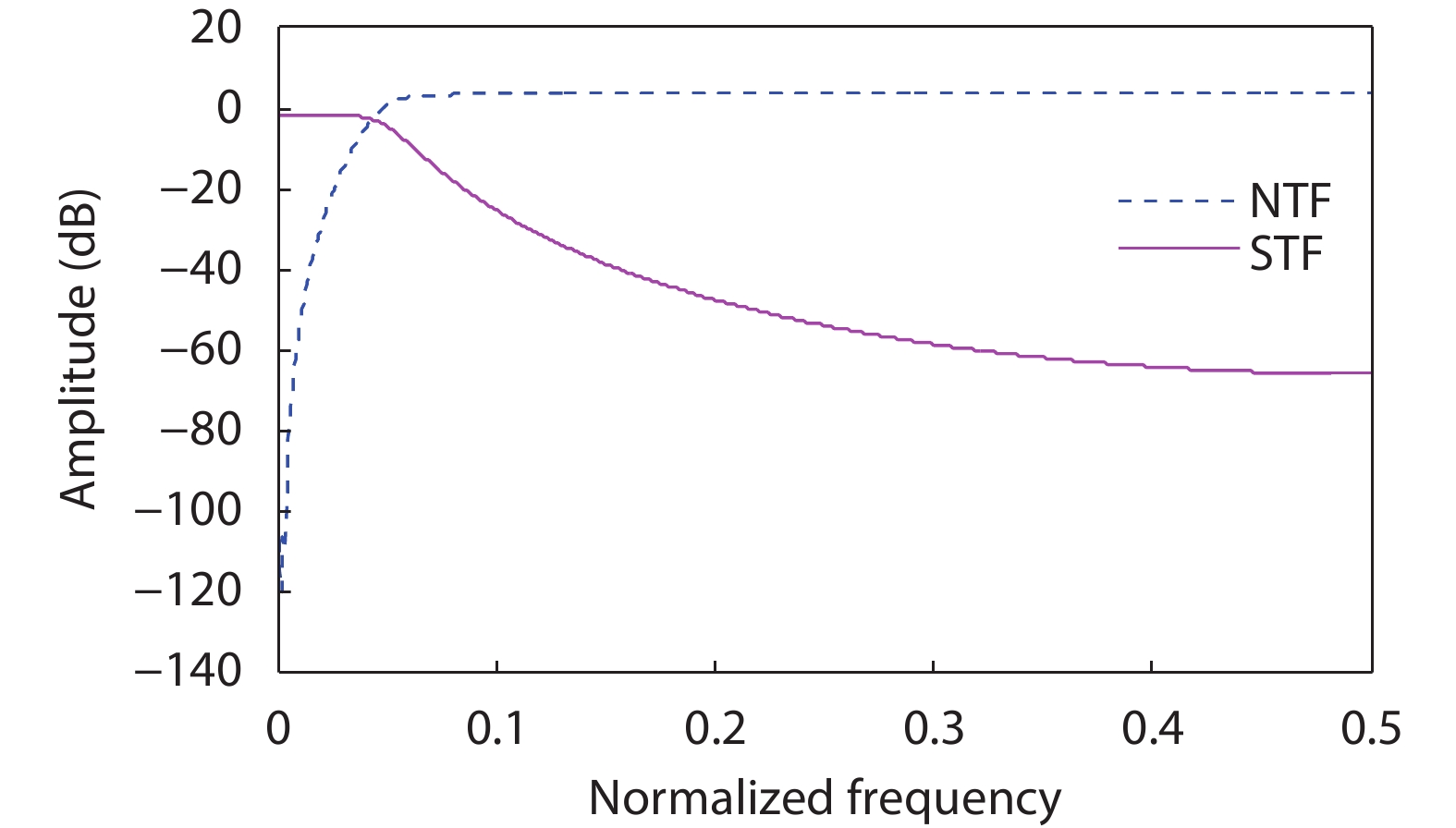
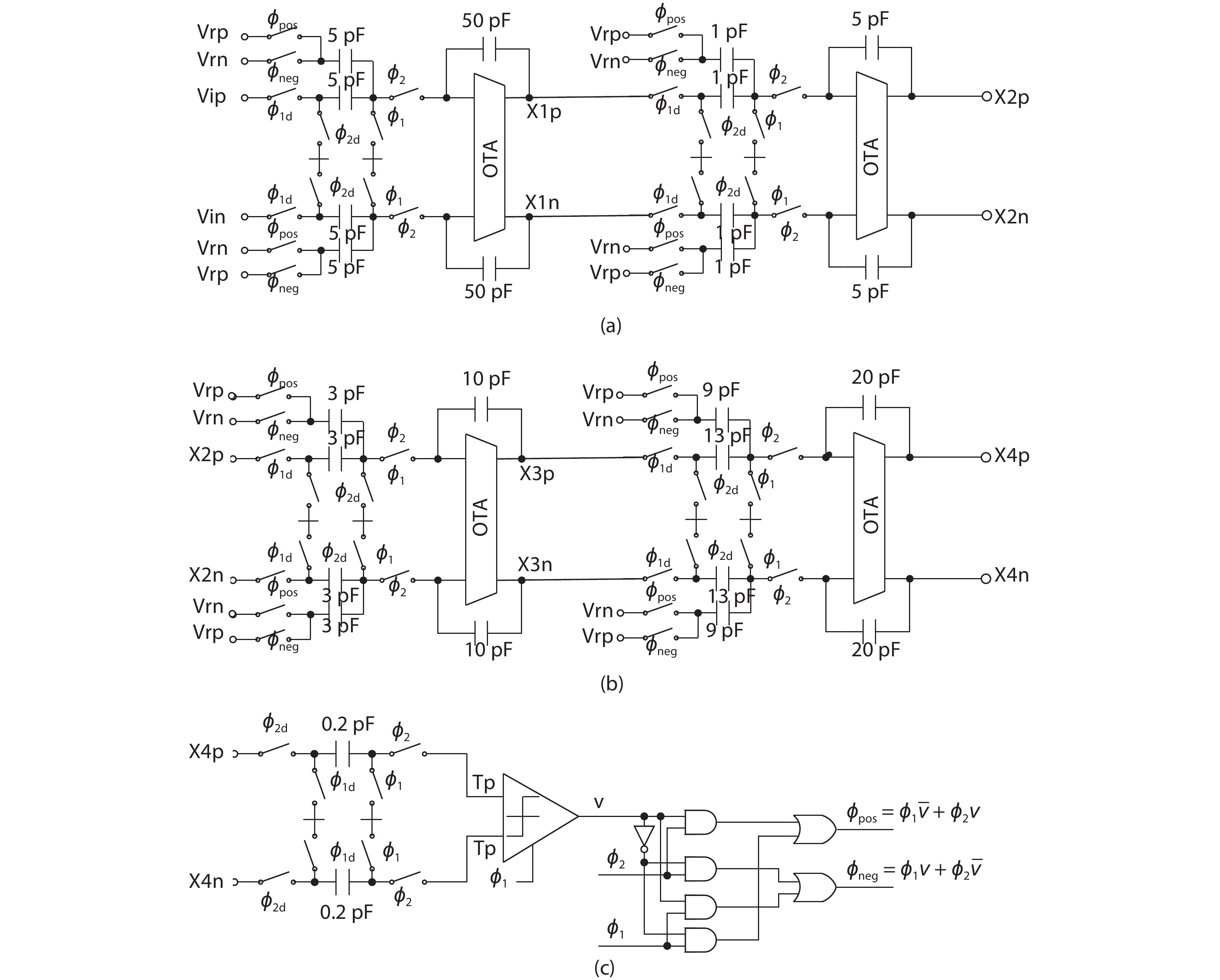
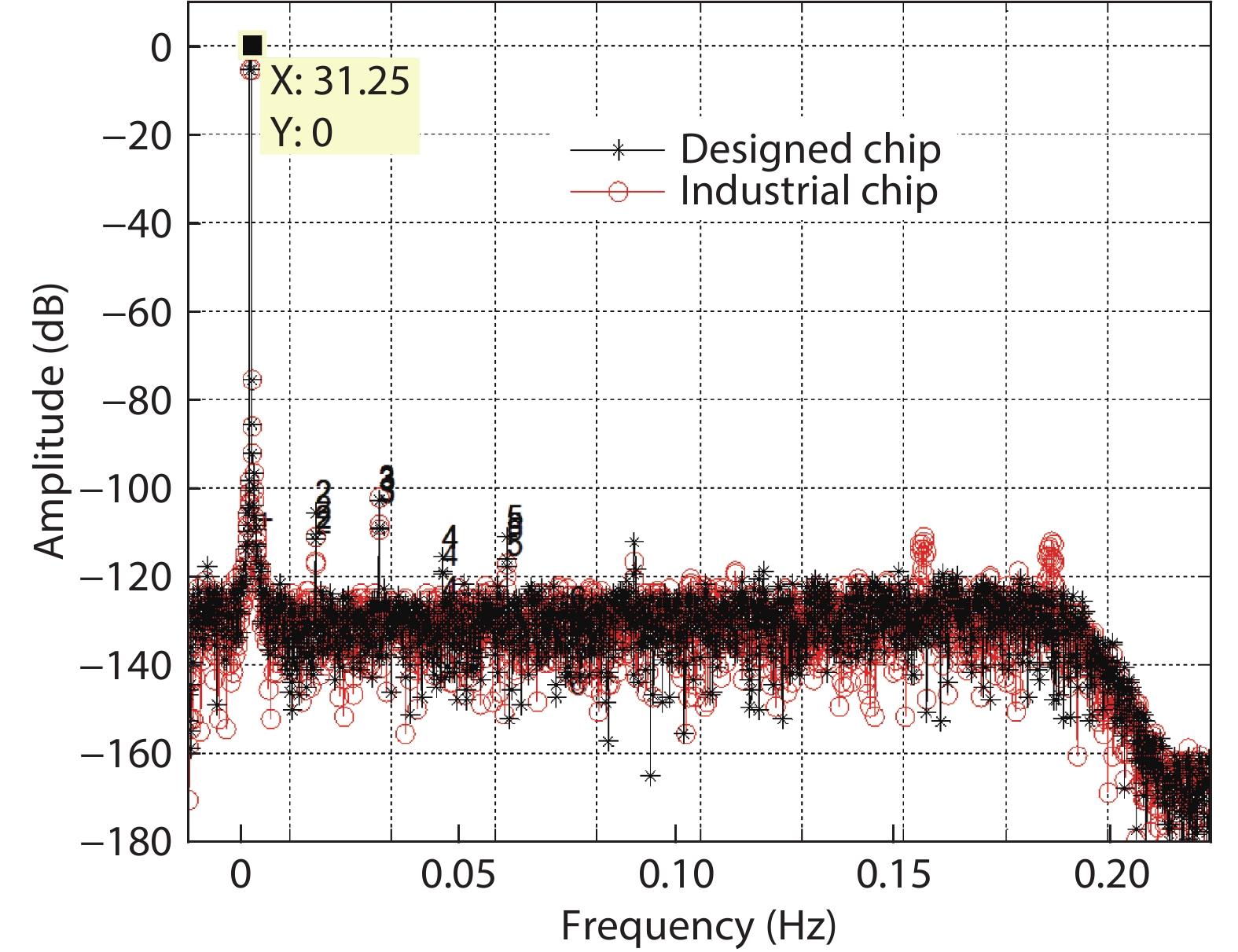
Oversampling sigma–delta (Σ–Δ) analog-to-digital converters (ADCs) are currently one of the most widely used architectures for high-resolution ADCs. The rapid development of integrated circuit manufacturing processes has allowed the realization of a high resolution in exchange for speed. Structurally, the Σ–Δ ADC is divided into two parts: a front-end analog modulator and a back-end digital filter. The performance of the front-end analog modulator has a marked influence on the entire Σ–Δ ADC system. In this paper, a 4-order single-loop switched-capacitor modulator with a CIFB (cascade-of-integrators feed-back) structure is proposed. Based on the chosen modulator architecture, the ASIC circuit is implemented using a chartered 0.35 μm CMOS process with a chip area of 1.72 × 0.75 mm2. The chip operates with a 3.3-V power supply and a power dissipation of 22 mW. According to the results, the performance of the designed modulator has been improved compared with a mature industrial chip and the effective number of bits (ENOB) was almost 18-bit.


J. Semicond.
2020, 41(6): 062601 doi: 10.1088/1674-4926/41/6/062601
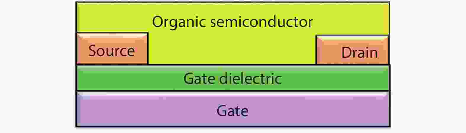
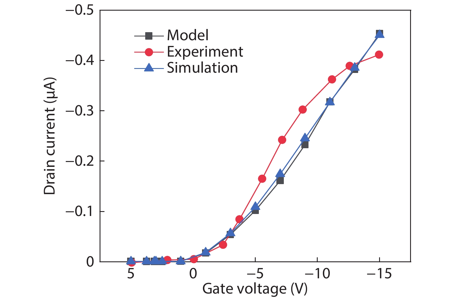
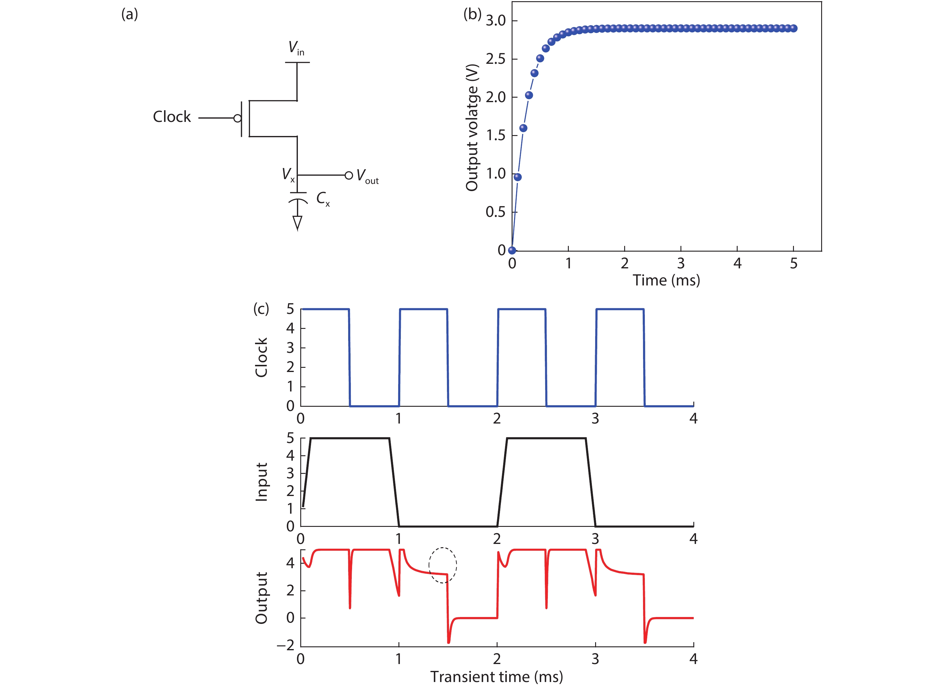
Steady state behavior analysis of organic thin film transistor (OTFTs) has been thoroughly researched in the past few decades. Yet, this static logic analysis has drawbacks of high power dissipation and high power consumption, and a large number of prerequisites in the number of transistors for the digital logic circuit application. Hence, to overcome these basic fundamental drawbacks of static logic, the dynamic logic study of organic thin film transistor has been analyzed in this paper. The fundamental basic of dynamic logic is a pass transistor for which logic high and logic low model is designed at an operating voltage of 5 V and frequency of 5 kHz. Additionally, the novel approach of analytical model for organic pass transistor (OPT) circuit is included and verified using MATLAB. The transient individualities of organic pass transistor OPT are examined through Atlas 2-D numerical device simulator. The reduction in the power dissipation along with additional voltage scaling and reduction in the clock frequency such as pipelining may further enable the applications into more complex VLSI ICs.


J. Semicond.
2020, 41(6): 062701 doi: 10.1088/1674-4926/41/6/062701
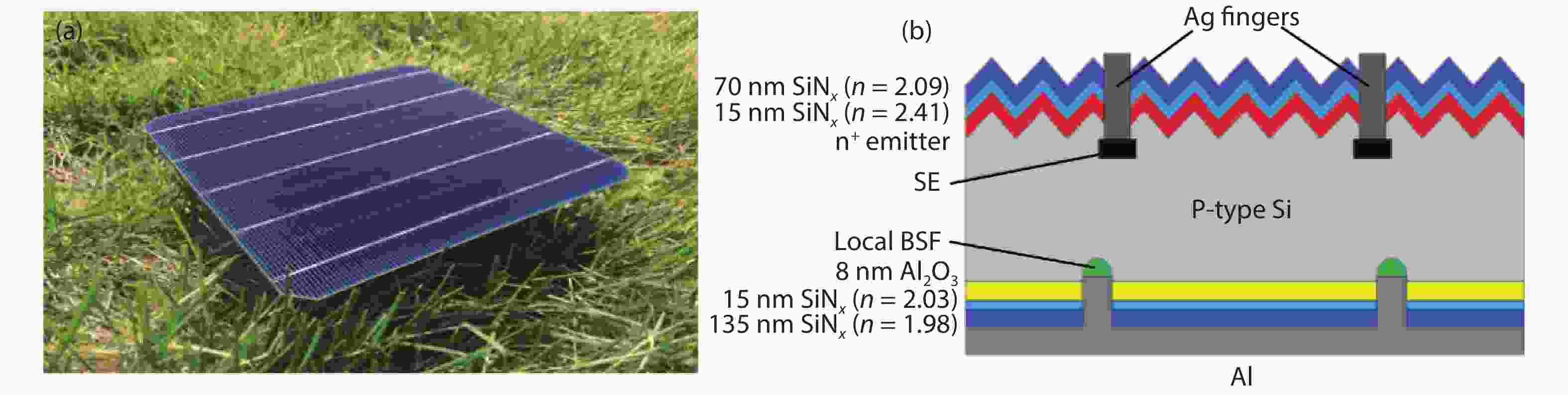
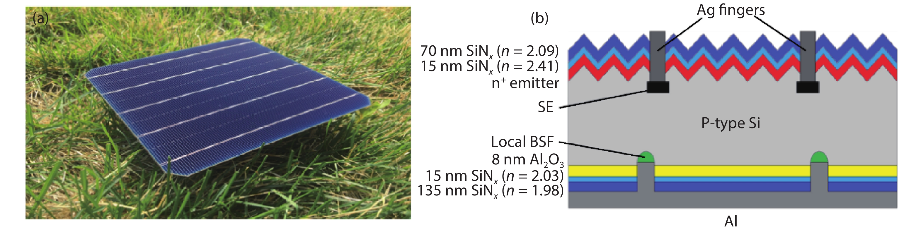
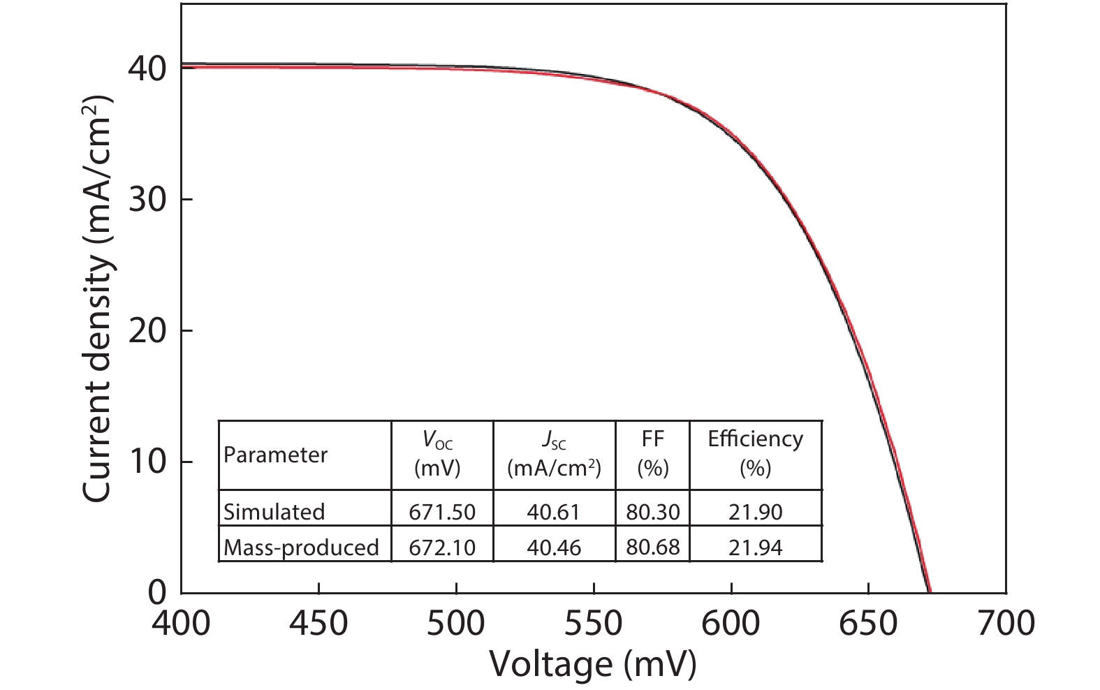
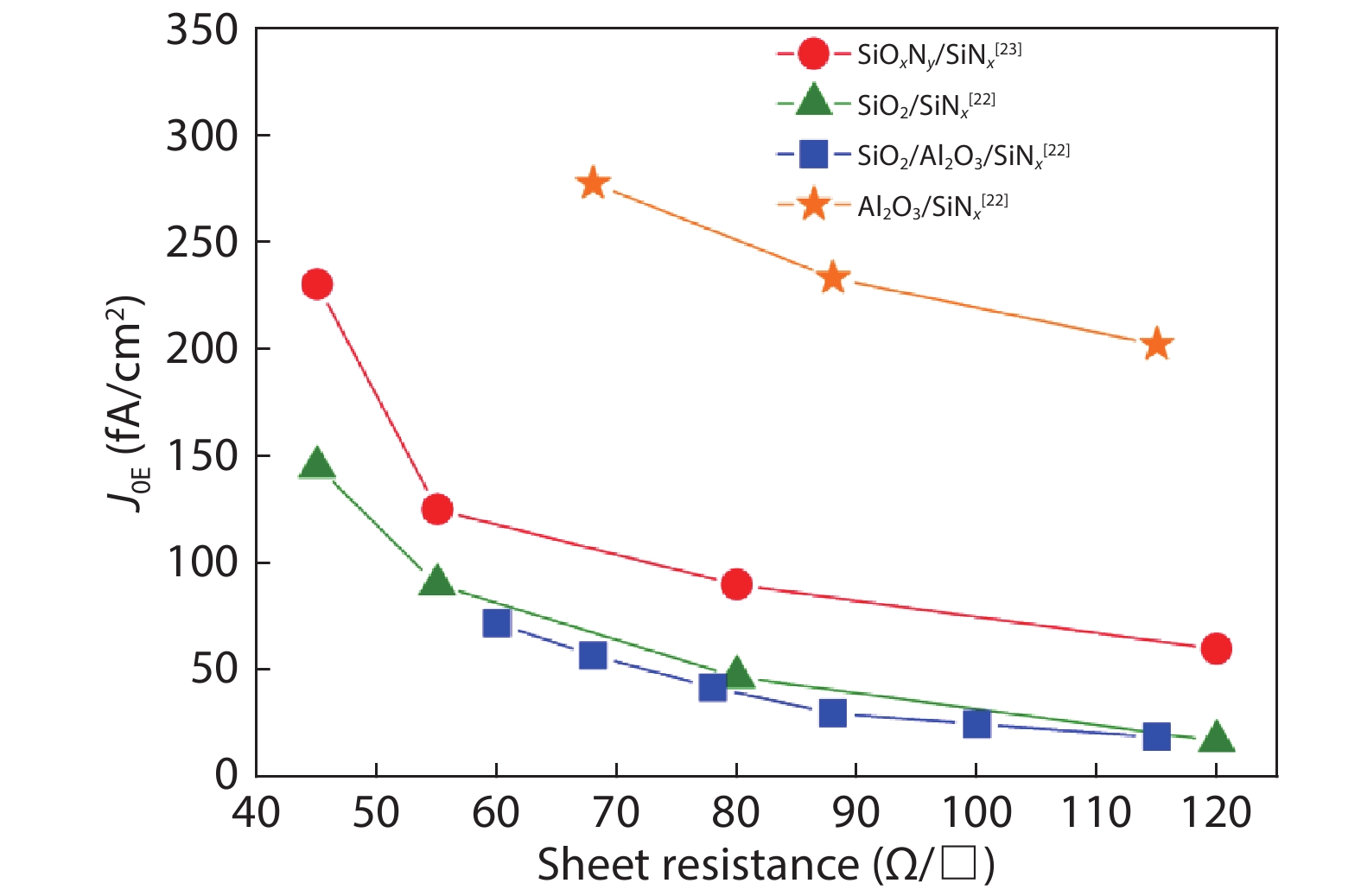
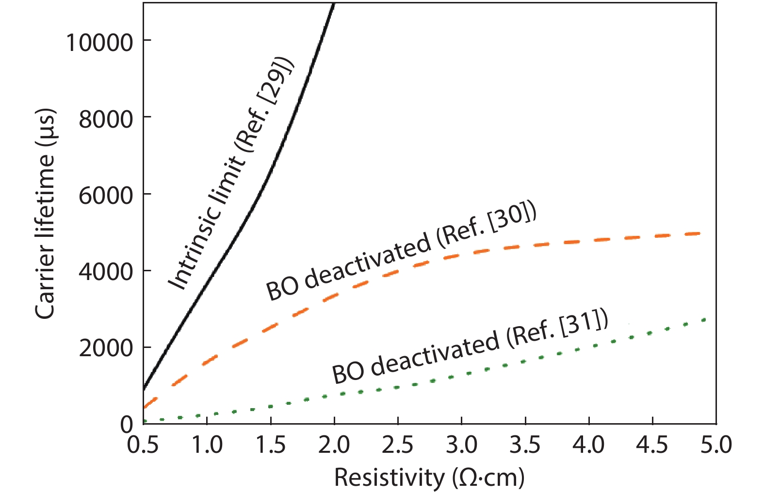
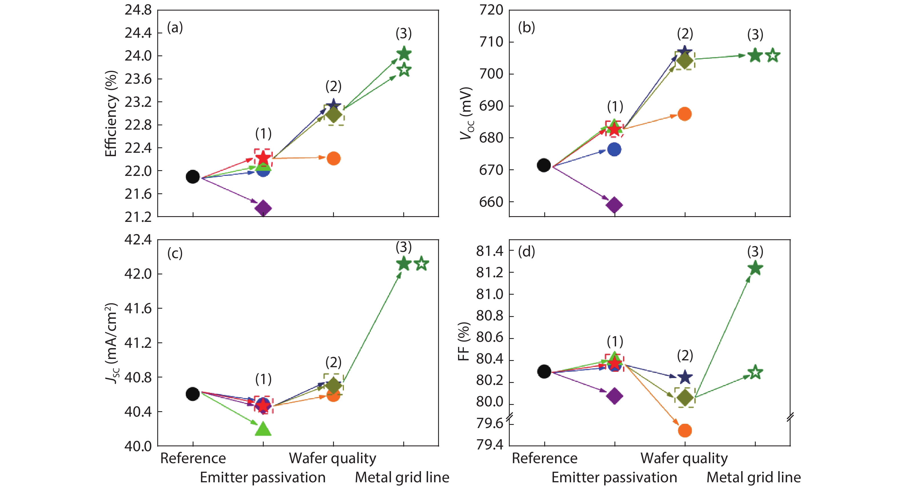
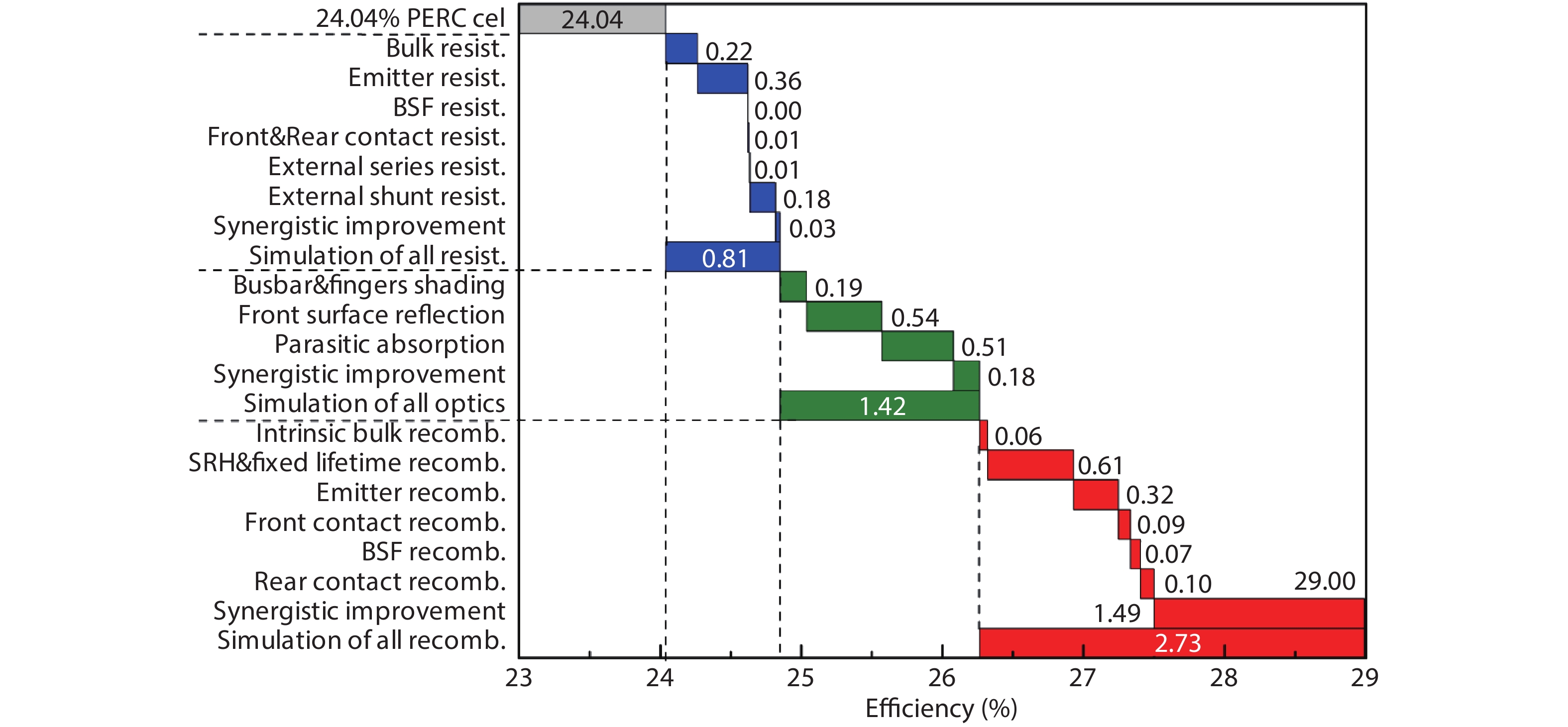
Mono-crystalline silicon solar cells with a passivated emitter rear contact (PERC) configuration have attracted extensive attention from both industry and scientific communities. A record efficiency of 24.06% on p-type silicon wafer and mass production efficiency around 22% have been demonstrated, mainly due to its superior rear side passivation. In this work, the PERC solar cells with a p-type silicon wafer were numerically studied in terms of the surface passivation, quality of silicon wafer and metal electrodes. A rational way to achieve a 24% mass-production efficiency was proposed. Free energy loss analyses were adopted to address the loss sources with respect to the limit efficiency of 29%, which provides a guideline for the design and manufacture of a high-efficiency PERC solar cell.


J. Semicond.
2020, 41(6): 062801 doi: 10.1088/1674-4926/41/6/062801
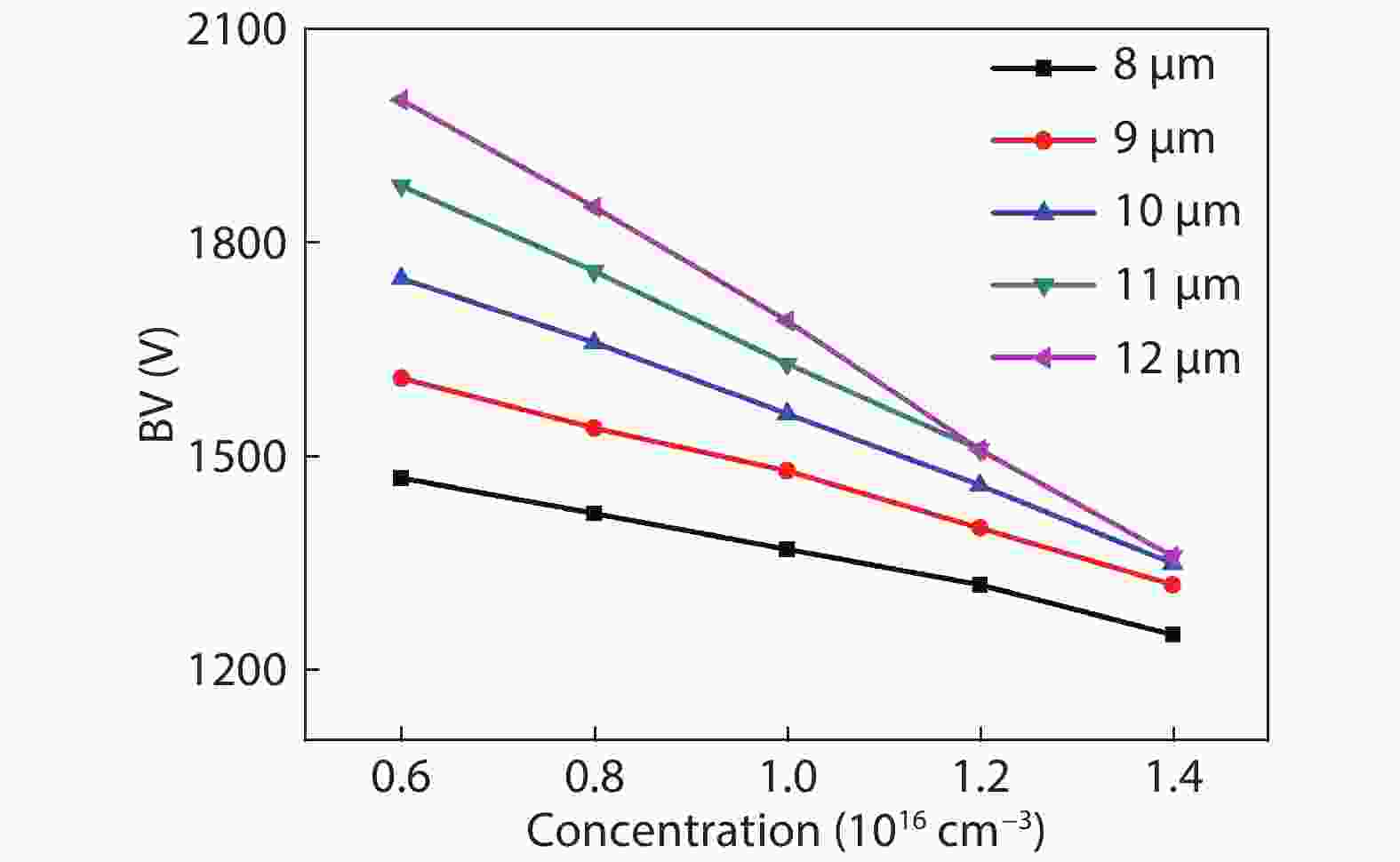
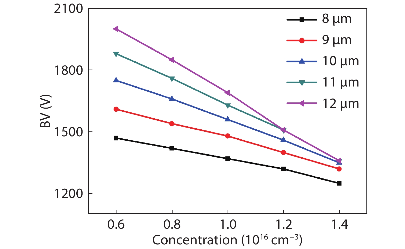
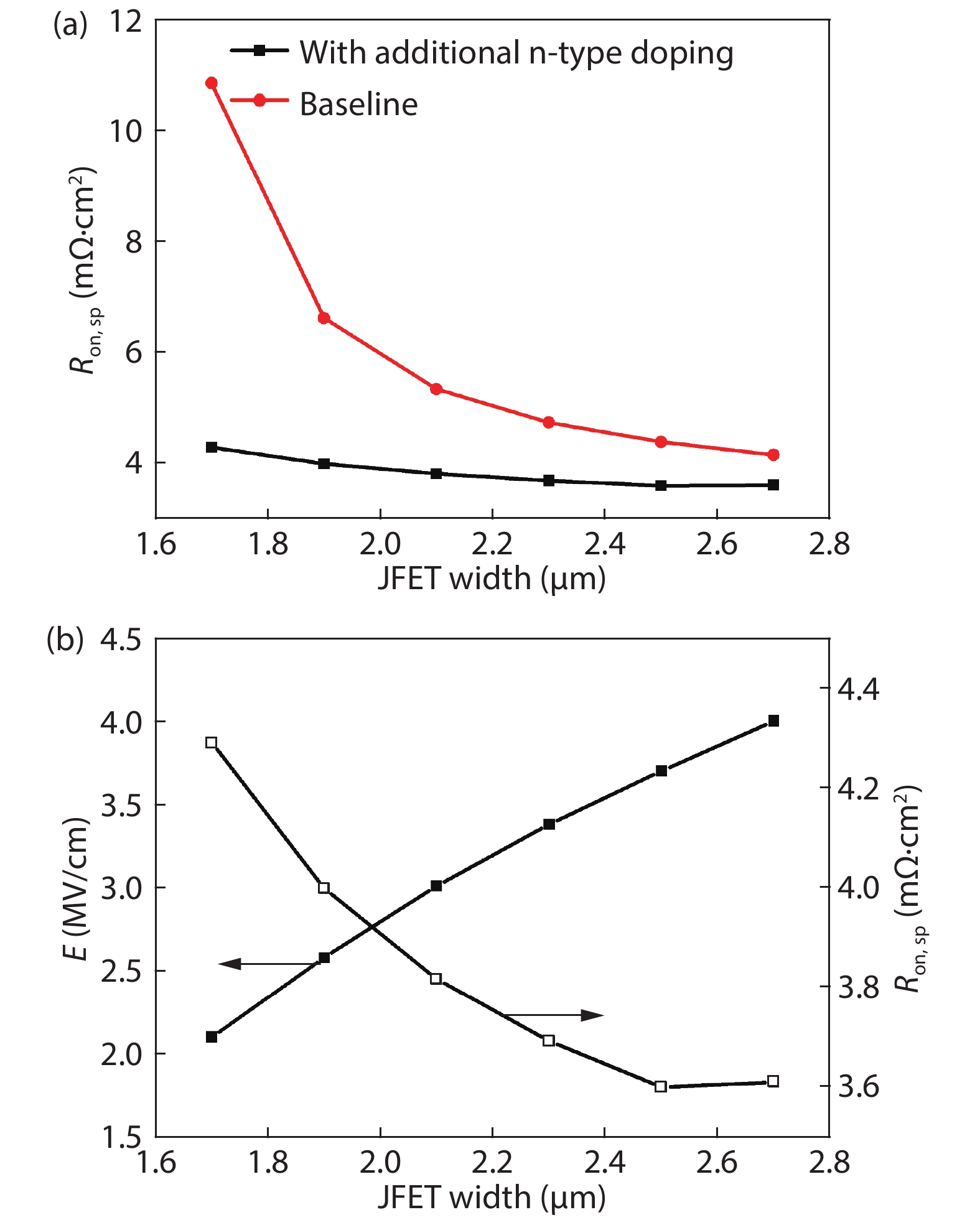
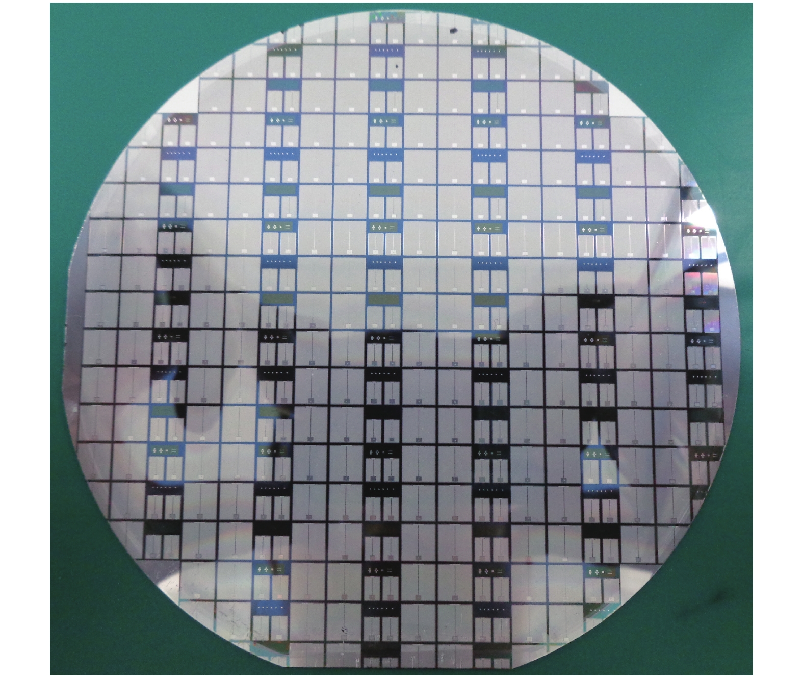
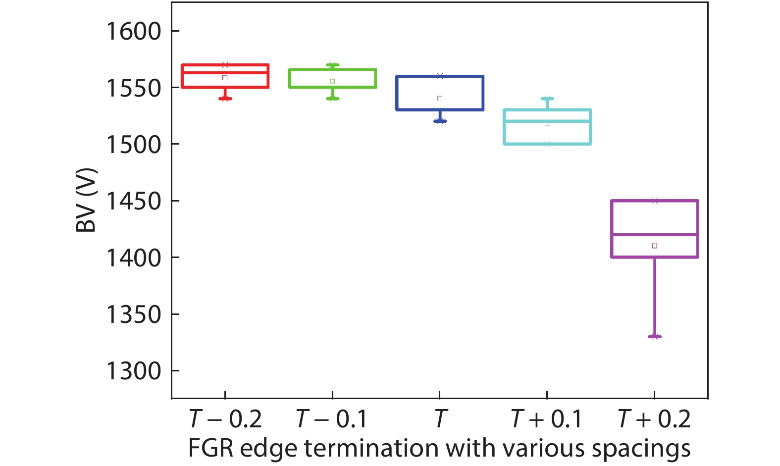
A 4H-SiC power MOSFET with specific on-resistance of 3.4 mΩ·cm2 and breakdown voltage exceeding 1.5 kV is designed and fabricated. Numerical simulations are carried out to optimize the electric field strength in gate oxide and at the surface of the semiconductor material in the edge termination region. Additional n-type implantation in JFET region is implemented to reduce the specific on-resistance. The typical leakage current is less than 1 μA at VDS = 1.4 kV. Drain–source current reaches 50 A at VDS = 0.75 V and VGS = 20 V corresponding to an on-resistance of 15 mΩ. The typical gate threshold voltage is 2.6 V.