


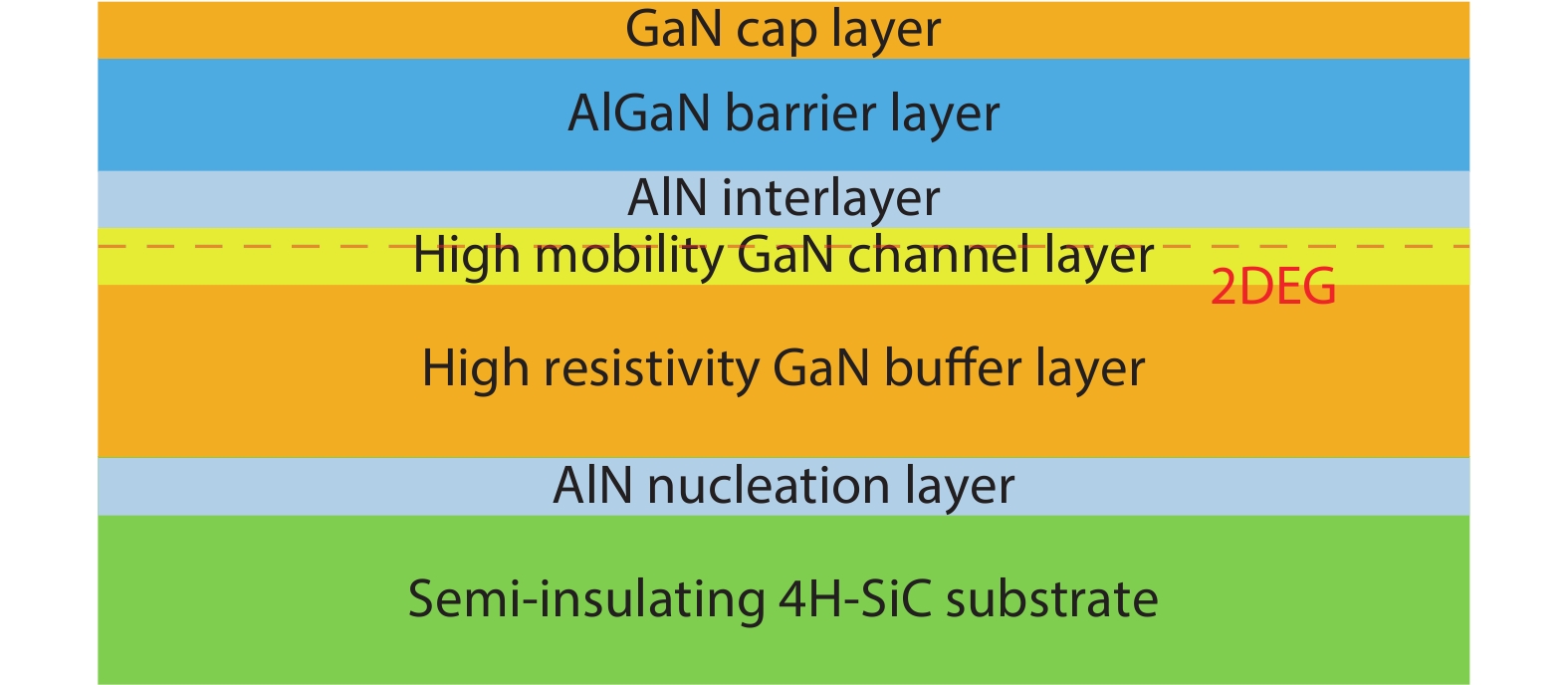
Fig. 1.
(Color online) The schematic of the grown AlGaN/GaN HEMT structure.
ARTICLES
Quan Wang1, 2, 3, Changxi Chen3, 4, Wei Li3, 4, Yanbin Qin3, 4, Lijuan Jiang3, 4, 5, Chun Feng3, 4, 5, Qian Wang3, 5, Hongling Xiao3, 4, 5, Xiufang Chen1, 2, Fengqi Liu3, 4, 5, Xiaoliang Wang3, 4, 5, , Xiangang Xu1, 2, and Zhanguo Wang3, 4
Corresponding author: Xiaoliang Wang, xlwang@semi.ac.cn; Xiangang Xu, xxu@sdu.edu.cn
Abstract: State-of-the-art AlGaN/GaN high electron mobility structures were grown on semi-insulating 4H-SiC substrates by MOCVD and X-band microwave power high electron mobility transistors were fabricated and characterized. Hall mobility of 2291.1 cm2/(V·s) and two-dimensional electron gas density of 9.954 × 1012 cm–2 were achieved at 300 K. The HEMT devices with a 0.45-μm gate length exhibited maximum drain current density as high as 1039.6 mA/mm and peak extrinsic transconductance of 229.7 mS/mm. The fT of 30.89 GHz and fmax of 38.71 GHz were measured on the device. Load-pull measurements were performed and analyzed under (–3.5, 28) V, (–3.5, 34) V and (–3.5, 40) V gate/drain direct current bias in class-AB, respectively. The uncooled device showed high linear power gain of 17.04 dB and high power-added efficiency of 50.56% at 8 GHz when drain biased at (–3.5, 28) V. In addition, when drain biased at (–3.5, 40) V, the device exhibited a saturation output power density up to 6.21 W/mm at 8 GHz, with a power gain of 11.94 dB and a power-added efficiency of 39.56%. Furthermore, the low fmax/fT ratio and the variation of the power sweep of the device at 8 GHz with drain bias voltage were analyzed.
Key words: AlGaN/GaN heterostructure, MOCVD, HEMTs, power amplifier
| [1] |
Khan M A, Kuznia J N, Bhattarai A R, et al. Metal semiconductor field effect transistor based on single crystal GaN. Appl Phys Lett, 1993, 62(15), 1786 doi: 10.1063/1.109549
|
| [2] |
Ambacher O, Smart J, Shealy J R, et al. Two-dimensional electron gases induced by spontaneous and piezoelectric polarization in undoped. J Appl Phys, 2000, 85(6), 3222 doi: 10.1063/1.369664
|
| [3] |
Jain S C, Willander M, Narayan J, et al. III-nitrides: Growth, characterization, and properties. J Appl Phys, 2000, 87(3), 965 doi: 10.1063/1.371971
|
| [4] |
Wang X L, Hu G X, Ma Z Y, et al. MOCVD-grown AlGaN/AlN/GaN HEMT structure with high mobility GaN thin layer as channel on SiC. Chin J Semicond, 2006, 27(9), 1521
|
| [5] |
Fletcher A, Nirmal D, Ajayan J, et al. An intensive study on assorted substrates suitable for high JFOM AlGaN/GaN HEMT. Silicon, 2020, 13(3), 1591 doi: 10.1007/s12633-020-00549-4
|
| [6] |
Gao Y, Zhang H, Zong Y, et al. 150 mm 4H-SiC substrate with low defect density. Mater Sci Forum, 2016, 858, 41 doi: 10.4028/www.scientific.net/MSF.858.41
|
| [7] |
Jang B K, Park J H, Choi J W, et al. Modified hot-zone design of growth cell for reducing the warpage of 6"-SiC wafer. Mater Sci Forum, 2020, 1004, 32 doi: 10.4028/www.scientific.net/MSF.1004.32
|
| [8] |
Mishra U K, Parikh P, Wu Y F. AlGaN/GaN HEMTs-an overview of device operation and applications. Proc IEEE, 2002, 90(6), 1022 doi: 10.1109/JPROC.2002.1021567
|
| [9] |
Pengelly R S. A review of GaN on SiC high electron-mobility power transistors and MMICs. IEEE Trans Microwave Theory Tech, 2012, 60(6), 1764 doi: 10.1109/TMTT.2012.2187535
|
| [10] |
Camarchia V, Quaglia R, Piacibello A, et al. A review of technologies and design techniques of millimeter-wave power amplifiers. IEEE Trans Microwave Theory Tech, 2020, 68(7), 2957 doi: 10.1109/TMTT.2020.2989792
|
| [11] |
Wang X L, Chen T S, Xiao H L, et al. High-performance 2 mm gate width GaN HEMTs on 6H-SiC with output power of 22.4W@8GHz. Solid-State Electron, 2008, 52(6), 926 doi: 10.1016/j.sse.2007.12.014
|
| [12] |
Wang X L, Chen T S, Xiao H L, et al. An internally-matched GaN HEMTs device with 45.2 W at 8 GHz for X-band application. Solid State Electron, 2009, 53(3), 332 doi: 10.1016/j.sse.2009.01.003
|
| [13] |
Wang Q, Wang X L, Xiao H L, et al. X-band GaN high electron mobility transistor power amplifier on 6H-SiC with 110 W output power. J Nanosci Nanotechnol, 2018, 18(11), 7451 doi: 10.1166/jnn.2018.16075
|
| [14] |
Mishra U K, Shen L, Kazior T E, et al. GaN-based RF power devices and amplifiers. Proc IEEE, 2008, 96(2), 287 doi: 10.1109/JPROC.2007.911060
|
| [15] |
Chen C, Sadler R, Wang D, et al. The interplay of thermal, time and Poole-Frenkel emission on the trap-based physical modeling of GaN HEMT drain characteristics. 2017 IEEE Compound Semiconductor Integrated Circuit Symposium (CSICS), 2017, 1
|
| [16] |
Kellogg K, Khandelwal S, Dunleavy L, et al. Characterization of thermal and trapping time constants in a GaN HEMT. 2020 94th ARFTG Microwave Measurement Symposium (ARFTG), 2020, 1
|
| [17] |
Zhang L Q, Wang P F. AlGaN/GaN HEMT with LPCVD deposited SiN and PECVD deposited SiCOH low-k passivation. Appl Phys Express, 2019, 12(3), 036501 doi: 10.7567/1882-0786/ab0139
|
| [18] |
Nakajima A, Itagaki K, Horio K. Effects of field plate on buffer trapping in AlGaN/GaN HEMTs. Phys Status Solidi C, 2009, 6(12), 2840 doi: 10.1002/pssc.200982557
|
| [19] |
Bi Y, Wang X L, Xiao H L, et al. The influence of the InGaN back-barrier on the properties of Al0.3Ga0.7N/AlN/GaN/InGaN/GaN structure. Eur Phys J-Appl Phys, 2011, 55(1), 10102 doi: 10.1051/epjap/2011110184
|
| [20] |
Shen L, Heikman S, Moran B, et al. AlGaN/AlN/GaN high-power microwave HEMT. IEEE Electron Device Lett, 2001, 22(10), 457 doi: 10.1109/55.954910
|
| [21] |
Yu E T, Dang X Z, Yu L S, et al. Schottky barrier engineering in III-V nitrides via the piezoelectric effect. Appl Phys Lett, 1998, 73(13), 1880 doi: 10.1063/1.122312
|
| [22] |
Gessmann T, Graff J W, Li Y L, et al. Ohmic contact technology in III-V nitrides using polarization effects in cap layers. IEEE Lester Eastman Conference on High Performance Devices, 2002, 492
|
| [23] |
Arulkumaran S, Egawa T, Ishikawa H. Studies on the influences of i-GaN, n-GaN, p-GaN and InGaN cap layers in AlGaN/GaN high-electron-mobility transistors. Jpn J Appl Phys, 2005, 44(5R), 2953 doi: 10.1143/jjap.44.2953
|
| [24] |
Gong J M, Wang Q, Yan J D, et al. Comparison of GaN/AlGaN/AlN/GaN HEMTs grown on sapphire with Fe-modulation-doped and unintentionally doped GaN buffer: Material growth and device fabrication. Chin Phys Lett, 2016, 33(11), 103 doi: 10.1088/0256-307x/33/11/117303
|
| [25] |
Singh M, Uren M J, Martin T, et al. 'Kink' in AlGaN/GaN-HEMTs: Floating buffer model. IEEE Trans Electron Devices, 2018, 65(9), 3746 doi: 10.1109/TED.2018.2860902
|
| [26] |
Fu L H, Lu H, Chen D J, et al. Field-dependent carrier trapping induced kink effect in AlGaN/GaN high electron mobility transistors. Appl Phys Lett, 2011, 98(17), 586 doi: 10.1063/1.3584861
|
| [27] |
Alim M A, Afrin S, Rezazadeh A A, et al. Thermal response and correlation between mobility and kink effect in GaN HEMTs. Microelectron Eng, 2020, 219, 111148.1 doi: 10.1016/j.mee.2019.111148
|
| [28] |
Wu Y. AlGaN/GaN microwave power high-mobility-transistors. PhD Dissertation, University of California, Santa Barbara, 1997
|
| [29] |
Gelmont B, Kim K, Shur M. Monte Carlo simulation of electron transport in gallium nitride. J Appl Phys, 1993, 74(3), 1818 doi: 10.1063/1.354787
|
| [30] |
Steven M. N-polar deep recess MISHEMTs for mm-wave applications. PhD Dissertation, University of California, Santa Barbara, 2018
|
| [31] |
Cripps S C. RF power amplifiers for wireless communications. Norwood, MA: Artech House, 2006
|
| [32] |
Darwish A M, Huebschman B D, Viveiros E, et al. Dependence of GaN HEMT millimeter-wave performance on temperature. IEEE Trans Microwave Theory Tech, 2009, 57(12), 3205 doi: 10.1109/TMTT.2009.2034050
|
| [33] |
Kühn J. AlGaN/GaN-HEMT power amplifiers with optimized power-added efficiency for X-band applications. KIT Scientific Publishing, 2011
|
| [34] |
Vetury R, Zhang N Q, Keller S, et al. The impact of surface states on the DC and RF characteristics of AlGaN/GaN HFETs. IEEE Trans Electron Devices, 2001, 48(3), 560 doi: 10.1109/16.906451
|
| [35] |
Chu R, Shen L, Fichtenbaum N, et al. Correlation between DC–RF dispersion and gate leakage in deeply recessed GaN/AlGaN/GaN HEMTs. IEEE Electron Device Lett, 2008, 29(4), 303 doi: 10.1109/LED.2008.917939
|
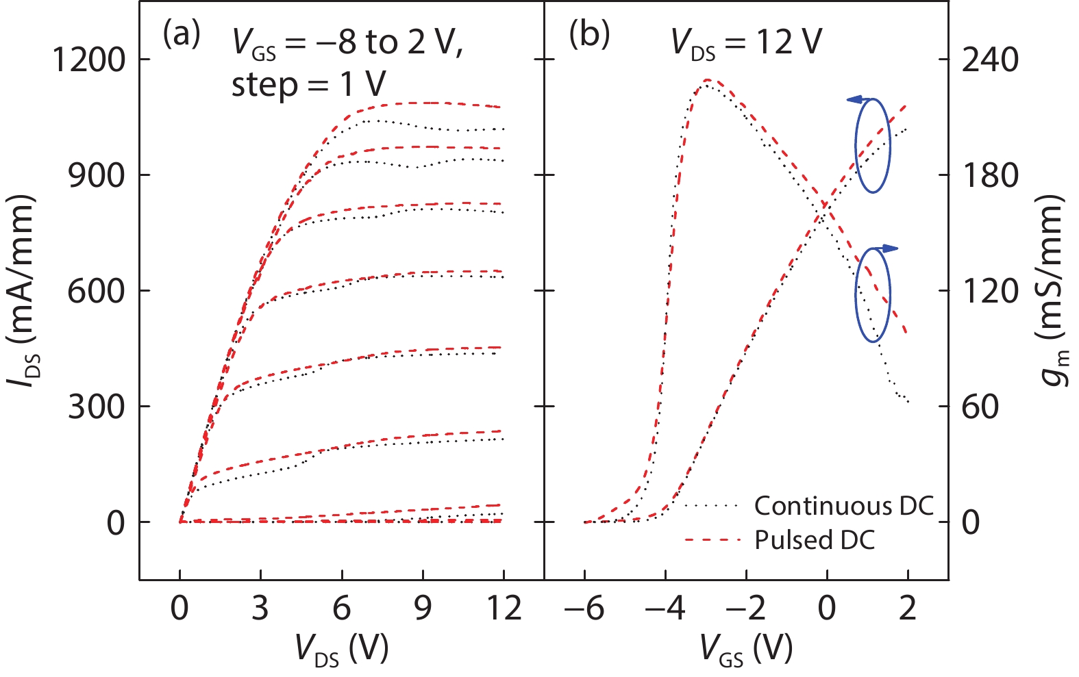
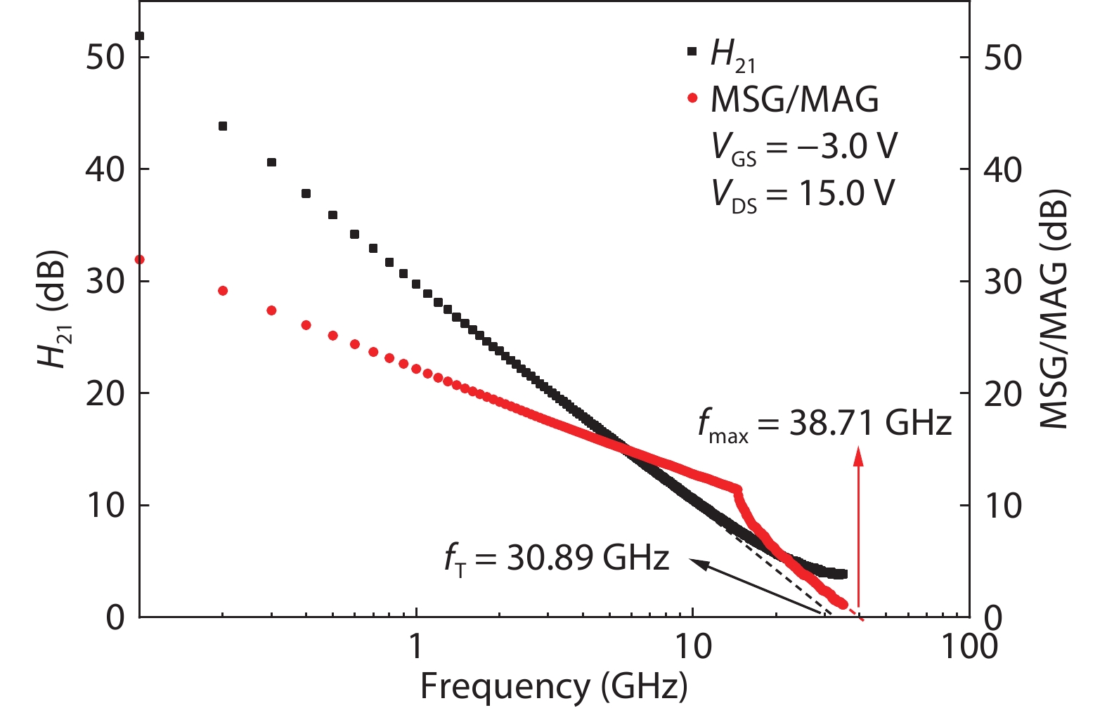
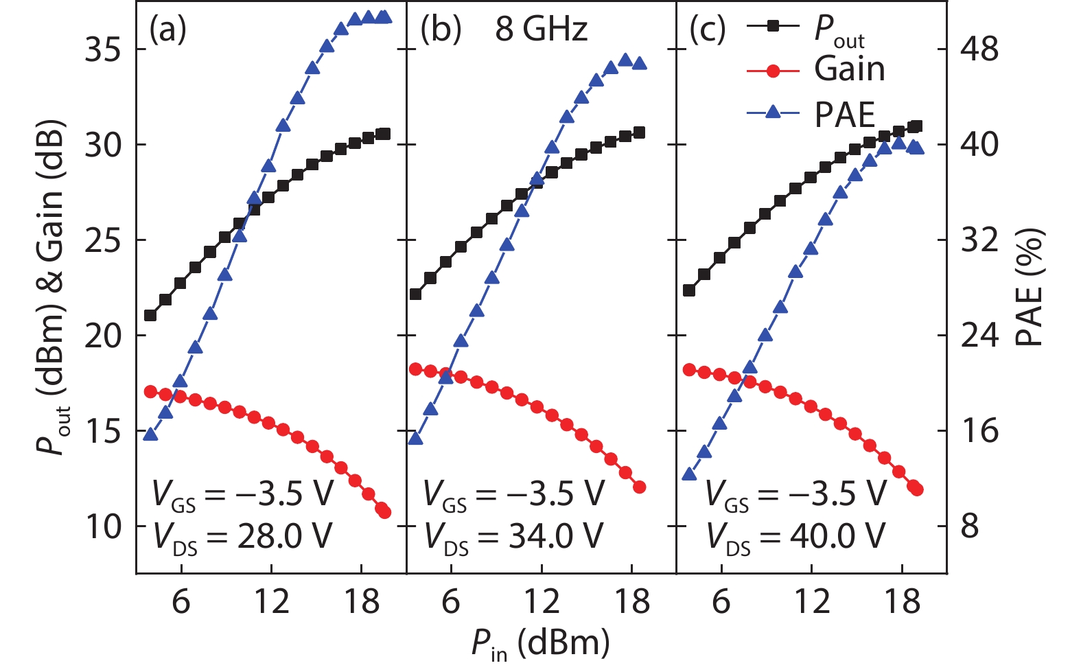
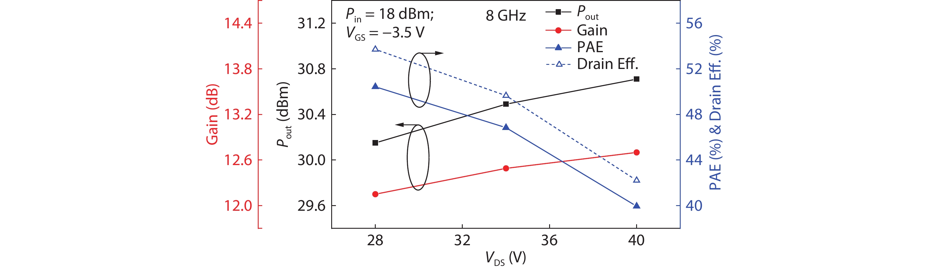
Table 1. The growth parameters of the AlGaN / GaN HEMT structure.
| Order | Material | Purpose | Thickness (nm) | Temperature (°C) |
| 1 | AlN | Nucleation layer | 50 | 1000–1050 |
| 2 | GaN | Buffer layer with high resistivity | 2000 | 1050 |
| 3 | GaN | High mobility channel layer | 100 | 1050 |
| 4 | AlN | Interlayer | 1 | 1000 |
| 5 | Al0.255Ga0.745N | Barrier layer | 21.5 | 1000 |
| 6 | GaN | Cap layer | 3 | 1050 |
 DownLoad: CSV
Table 2. The detailed measurement results of power performances of the fabricated AlGaN/GaN HEMT device.
| DC bias (VGS, VDS) (V) | Pout (max) (dBm) | Pin (dBm) | G (dB) | PAE (%) | G (compression) (dB) | G (linear) (dB) | Pout density (saturated) (W/mm) |
| (–3.5, 28) | 30.54 | 19.54 | 11.00 | 50.56 | 6 | 17.04 | 5.66 |
| (–3.5, 34) | 30.61 | 18.52 | 12.09 | 46.67 | 6 | 18.22 | 5.75 |
| (–3.5, 40) | 30.94 | 19.00 | 11.94 | 39.56 | 6 | 18.19 | 6.21 |
DownLoad: CSV
Table 3. The calculated possible output power and drain efficiency corresponding to different VDS from 28 to 40 V when VGS = –3.5 V.
| DC bias (VGS, VDS) (V) | VDS − VK (V) | PDC (W/mm) | PRF (W/mm) (VK = 4.2 V) | ηD (%) |
| (–3.5, 28) | 23.80 | 10.68 | 6.53 | 61.09 |
| (–3.5, 34) | 29.80 | 12.97 | 8.17 | 62.99 |
| (–3.5, 40) | 35.80 | 15.26 | 9.82 | 64.32 |
DownLoad: CSV
| [1] |
Khan M A, Kuznia J N, Bhattarai A R, et al. Metal semiconductor field effect transistor based on single crystal GaN. Appl Phys Lett, 1993, 62(15), 1786 doi: 10.1063/1.109549
|
| [2] |
Ambacher O, Smart J, Shealy J R, et al. Two-dimensional electron gases induced by spontaneous and piezoelectric polarization in undoped. J Appl Phys, 2000, 85(6), 3222 doi: 10.1063/1.369664
|
| [3] |
Jain S C, Willander M, Narayan J, et al. III-nitrides: Growth, characterization, and properties. J Appl Phys, 2000, 87(3), 965 doi: 10.1063/1.371971
|
| [4] |
Wang X L, Hu G X, Ma Z Y, et al. MOCVD-grown AlGaN/AlN/GaN HEMT structure with high mobility GaN thin layer as channel on SiC. Chin J Semicond, 2006, 27(9), 1521
|
| [5] |
Fletcher A, Nirmal D, Ajayan J, et al. An intensive study on assorted substrates suitable for high JFOM AlGaN/GaN HEMT. Silicon, 2020, 13(3), 1591 doi: 10.1007/s12633-020-00549-4
|
| [6] |
Gao Y, Zhang H, Zong Y, et al. 150 mm 4H-SiC substrate with low defect density. Mater Sci Forum, 2016, 858, 41 doi: 10.4028/www.scientific.net/MSF.858.41
|
| [7] |
Jang B K, Park J H, Choi J W, et al. Modified hot-zone design of growth cell for reducing the warpage of 6"-SiC wafer. Mater Sci Forum, 2020, 1004, 32 doi: 10.4028/www.scientific.net/MSF.1004.32
|
| [8] |
Mishra U K, Parikh P, Wu Y F. AlGaN/GaN HEMTs-an overview of device operation and applications. Proc IEEE, 2002, 90(6), 1022 doi: 10.1109/JPROC.2002.1021567
|
| [9] |
Pengelly R S. A review of GaN on SiC high electron-mobility power transistors and MMICs. IEEE Trans Microwave Theory Tech, 2012, 60(6), 1764 doi: 10.1109/TMTT.2012.2187535
|
| [10] |
Camarchia V, Quaglia R, Piacibello A, et al. A review of technologies and design techniques of millimeter-wave power amplifiers. IEEE Trans Microwave Theory Tech, 2020, 68(7), 2957 doi: 10.1109/TMTT.2020.2989792
|
| [11] |
Wang X L, Chen T S, Xiao H L, et al. High-performance 2 mm gate width GaN HEMTs on 6H-SiC with output power of 22.4W@8GHz. Solid-State Electron, 2008, 52(6), 926 doi: 10.1016/j.sse.2007.12.014
|
| [12] |
Wang X L, Chen T S, Xiao H L, et al. An internally-matched GaN HEMTs device with 45.2 W at 8 GHz for X-band application. Solid State Electron, 2009, 53(3), 332 doi: 10.1016/j.sse.2009.01.003
|
| [13] |
Wang Q, Wang X L, Xiao H L, et al. X-band GaN high electron mobility transistor power amplifier on 6H-SiC with 110 W output power. J Nanosci Nanotechnol, 2018, 18(11), 7451 doi: 10.1166/jnn.2018.16075
|
| [14] |
Mishra U K, Shen L, Kazior T E, et al. GaN-based RF power devices and amplifiers. Proc IEEE, 2008, 96(2), 287 doi: 10.1109/JPROC.2007.911060
|
| [15] |
Chen C, Sadler R, Wang D, et al. The interplay of thermal, time and Poole-Frenkel emission on the trap-based physical modeling of GaN HEMT drain characteristics. 2017 IEEE Compound Semiconductor Integrated Circuit Symposium (CSICS), 2017, 1
|
| [16] |
Kellogg K, Khandelwal S, Dunleavy L, et al. Characterization of thermal and trapping time constants in a GaN HEMT. 2020 94th ARFTG Microwave Measurement Symposium (ARFTG), 2020, 1
|
| [17] |
Zhang L Q, Wang P F. AlGaN/GaN HEMT with LPCVD deposited SiN and PECVD deposited SiCOH low-k passivation. Appl Phys Express, 2019, 12(3), 036501 doi: 10.7567/1882-0786/ab0139
|
| [18] |
Nakajima A, Itagaki K, Horio K. Effects of field plate on buffer trapping in AlGaN/GaN HEMTs. Phys Status Solidi C, 2009, 6(12), 2840 doi: 10.1002/pssc.200982557
|
| [19] |
Bi Y, Wang X L, Xiao H L, et al. The influence of the InGaN back-barrier on the properties of Al0.3Ga0.7N/AlN/GaN/InGaN/GaN structure. Eur Phys J-Appl Phys, 2011, 55(1), 10102 doi: 10.1051/epjap/2011110184
|
| [20] |
Shen L, Heikman S, Moran B, et al. AlGaN/AlN/GaN high-power microwave HEMT. IEEE Electron Device Lett, 2001, 22(10), 457 doi: 10.1109/55.954910
|
| [21] |
Yu E T, Dang X Z, Yu L S, et al. Schottky barrier engineering in III-V nitrides via the piezoelectric effect. Appl Phys Lett, 1998, 73(13), 1880 doi: 10.1063/1.122312
|
| [22] |
Gessmann T, Graff J W, Li Y L, et al. Ohmic contact technology in III-V nitrides using polarization effects in cap layers. IEEE Lester Eastman Conference on High Performance Devices, 2002, 492
|
| [23] |
Arulkumaran S, Egawa T, Ishikawa H. Studies on the influences of i-GaN, n-GaN, p-GaN and InGaN cap layers in AlGaN/GaN high-electron-mobility transistors. Jpn J Appl Phys, 2005, 44(5R), 2953 doi: 10.1143/jjap.44.2953
|
| [24] |
Gong J M, Wang Q, Yan J D, et al. Comparison of GaN/AlGaN/AlN/GaN HEMTs grown on sapphire with Fe-modulation-doped and unintentionally doped GaN buffer: Material growth and device fabrication. Chin Phys Lett, 2016, 33(11), 103 doi: 10.1088/0256-307x/33/11/117303
|
| [25] |
Singh M, Uren M J, Martin T, et al. 'Kink' in AlGaN/GaN-HEMTs: Floating buffer model. IEEE Trans Electron Devices, 2018, 65(9), 3746 doi: 10.1109/TED.2018.2860902
|
| [26] |
Fu L H, Lu H, Chen D J, et al. Field-dependent carrier trapping induced kink effect in AlGaN/GaN high electron mobility transistors. Appl Phys Lett, 2011, 98(17), 586 doi: 10.1063/1.3584861
|
| [27] |
Alim M A, Afrin S, Rezazadeh A A, et al. Thermal response and correlation between mobility and kink effect in GaN HEMTs. Microelectron Eng, 2020, 219, 111148.1 doi: 10.1016/j.mee.2019.111148
|
| [28] |
Wu Y. AlGaN/GaN microwave power high-mobility-transistors. PhD Dissertation, University of California, Santa Barbara, 1997
|
| [29] |
Gelmont B, Kim K, Shur M. Monte Carlo simulation of electron transport in gallium nitride. J Appl Phys, 1993, 74(3), 1818 doi: 10.1063/1.354787
|
| [30] |
Steven M. N-polar deep recess MISHEMTs for mm-wave applications. PhD Dissertation, University of California, Santa Barbara, 2018
|
| [31] |
Cripps S C. RF power amplifiers for wireless communications. Norwood, MA: Artech House, 2006
|
| [32] |
Darwish A M, Huebschman B D, Viveiros E, et al. Dependence of GaN HEMT millimeter-wave performance on temperature. IEEE Trans Microwave Theory Tech, 2009, 57(12), 3205 doi: 10.1109/TMTT.2009.2034050
|
| [33] |
Kühn J. AlGaN/GaN-HEMT power amplifiers with optimized power-added efficiency for X-band applications. KIT Scientific Publishing, 2011
|
| [34] |
Vetury R, Zhang N Q, Keller S, et al. The impact of surface states on the DC and RF characteristics of AlGaN/GaN HFETs. IEEE Trans Electron Devices, 2001, 48(3), 560 doi: 10.1109/16.906451
|
| [35] |
Chu R, Shen L, Fichtenbaum N, et al. Correlation between DC–RF dispersion and gate leakage in deeply recessed GaN/AlGaN/GaN HEMTs. IEEE Electron Device Lett, 2008, 29(4), 303 doi: 10.1109/LED.2008.917939
|


Article views: 2592 Times PDF downloads: 159 Times Cited by: 0 Times
Received: 26 April 2021 Revised: 01 June 2021 Online: Uncorrected proof: 18 June 2021Accepted Manuscript: 18 June 2021Published: 03 December 2021
| Citation: |
Quan Wang, Changxi Chen, Wei Li, Yanbin Qin, Lijuan Jiang, Chun Feng, Qian Wang, Hongling Xiao, Xiufang Chen, Fengqi Liu, Xiaoliang Wang, Xiangang Xu, Zhanguo Wang. Fabrication and characterization of AlGaN/GaN HEMTs with high power gain and efficiency at 8 GHz[J]. Journal of Semiconductors, 2021, 42(12): 122802. doi: 10.1088/1674-4926/42/12/122802
Q Wang, C X Chen, W Li, Y B Qin, L J Jiang, C Feng, Q Wang, H L Xiao, X F Chen, F Q Liu, X L Wang, X G Xu, Z G Wang, Fabrication and characterization of AlGaN/GaN HEMTs with high power gain and efficiency at 8 GHz[J]. J. Semicond., 2021, 42(12): 122802. doi: 10.1088/1674-4926/42/12/122802.
Export: BibTex EndNote

|
| [1] |
Khan M A, Kuznia J N, Bhattarai A R, et al. Metal semiconductor field effect transistor based on single crystal GaN. Appl Phys Lett, 1993, 62(15), 1786 doi: 10.1063/1.109549
|
| [2] |
Ambacher O, Smart J, Shealy J R, et al. Two-dimensional electron gases induced by spontaneous and piezoelectric polarization in undoped. J Appl Phys, 2000, 85(6), 3222 doi: 10.1063/1.369664
|
| [3] |
Jain S C, Willander M, Narayan J, et al. III-nitrides: Growth, characterization, and properties. J Appl Phys, 2000, 87(3), 965 doi: 10.1063/1.371971
|
| [4] |
Wang X L, Hu G X, Ma Z Y, et al. MOCVD-grown AlGaN/AlN/GaN HEMT structure with high mobility GaN thin layer as channel on SiC. Chin J Semicond, 2006, 27(9), 1521
|
| [5] |
Fletcher A, Nirmal D, Ajayan J, et al. An intensive study on assorted substrates suitable for high JFOM AlGaN/GaN HEMT. Silicon, 2020, 13(3), 1591 doi: 10.1007/s12633-020-00549-4
|
| [6] |
Gao Y, Zhang H, Zong Y, et al. 150 mm 4H-SiC substrate with low defect density. Mater Sci Forum, 2016, 858, 41 doi: 10.4028/www.scientific.net/MSF.858.41
|
| [7] |
Jang B K, Park J H, Choi J W, et al. Modified hot-zone design of growth cell for reducing the warpage of 6"-SiC wafer. Mater Sci Forum, 2020, 1004, 32 doi: 10.4028/www.scientific.net/MSF.1004.32
|
| [8] |
Mishra U K, Parikh P, Wu Y F. AlGaN/GaN HEMTs-an overview of device operation and applications. Proc IEEE, 2002, 90(6), 1022 doi: 10.1109/JPROC.2002.1021567
|
| [9] |
Pengelly R S. A review of GaN on SiC high electron-mobility power transistors and MMICs. IEEE Trans Microwave Theory Tech, 2012, 60(6), 1764 doi: 10.1109/TMTT.2012.2187535
|
| [10] |
Camarchia V, Quaglia R, Piacibello A, et al. A review of technologies and design techniques of millimeter-wave power amplifiers. IEEE Trans Microwave Theory Tech, 2020, 68(7), 2957 doi: 10.1109/TMTT.2020.2989792
|
| [11] |
Wang X L, Chen T S, Xiao H L, et al. High-performance 2 mm gate width GaN HEMTs on 6H-SiC with output power of 22.4W@8GHz. Solid-State Electron, 2008, 52(6), 926 doi: 10.1016/j.sse.2007.12.014
|
| [12] |
Wang X L, Chen T S, Xiao H L, et al. An internally-matched GaN HEMTs device with 45.2 W at 8 GHz for X-band application. Solid State Electron, 2009, 53(3), 332 doi: 10.1016/j.sse.2009.01.003
|
| [13] |
Wang Q, Wang X L, Xiao H L, et al. X-band GaN high electron mobility transistor power amplifier on 6H-SiC with 110 W output power. J Nanosci Nanotechnol, 2018, 18(11), 7451 doi: 10.1166/jnn.2018.16075
|
| [14] |
Mishra U K, Shen L, Kazior T E, et al. GaN-based RF power devices and amplifiers. Proc IEEE, 2008, 96(2), 287 doi: 10.1109/JPROC.2007.911060
|
| [15] |
Chen C, Sadler R, Wang D, et al. The interplay of thermal, time and Poole-Frenkel emission on the trap-based physical modeling of GaN HEMT drain characteristics. 2017 IEEE Compound Semiconductor Integrated Circuit Symposium (CSICS), 2017, 1
|
| [16] |
Kellogg K, Khandelwal S, Dunleavy L, et al. Characterization of thermal and trapping time constants in a GaN HEMT. 2020 94th ARFTG Microwave Measurement Symposium (ARFTG), 2020, 1
|
| [17] |
Zhang L Q, Wang P F. AlGaN/GaN HEMT with LPCVD deposited SiN and PECVD deposited SiCOH low-k passivation. Appl Phys Express, 2019, 12(3), 036501 doi: 10.7567/1882-0786/ab0139
|
| [18] |
Nakajima A, Itagaki K, Horio K. Effects of field plate on buffer trapping in AlGaN/GaN HEMTs. Phys Status Solidi C, 2009, 6(12), 2840 doi: 10.1002/pssc.200982557
|
| [19] |
Bi Y, Wang X L, Xiao H L, et al. The influence of the InGaN back-barrier on the properties of Al0.3Ga0.7N/AlN/GaN/InGaN/GaN structure. Eur Phys J-Appl Phys, 2011, 55(1), 10102 doi: 10.1051/epjap/2011110184
|
| [20] |
Shen L, Heikman S, Moran B, et al. AlGaN/AlN/GaN high-power microwave HEMT. IEEE Electron Device Lett, 2001, 22(10), 457 doi: 10.1109/55.954910
|
| [21] |
Yu E T, Dang X Z, Yu L S, et al. Schottky barrier engineering in III-V nitrides via the piezoelectric effect. Appl Phys Lett, 1998, 73(13), 1880 doi: 10.1063/1.122312
|
| [22] |
Gessmann T, Graff J W, Li Y L, et al. Ohmic contact technology in III-V nitrides using polarization effects in cap layers. IEEE Lester Eastman Conference on High Performance Devices, 2002, 492
|
| [23] |
Arulkumaran S, Egawa T, Ishikawa H. Studies on the influences of i-GaN, n-GaN, p-GaN and InGaN cap layers in AlGaN/GaN high-electron-mobility transistors. Jpn J Appl Phys, 2005, 44(5R), 2953 doi: 10.1143/jjap.44.2953
|
| [24] |
Gong J M, Wang Q, Yan J D, et al. Comparison of GaN/AlGaN/AlN/GaN HEMTs grown on sapphire with Fe-modulation-doped and unintentionally doped GaN buffer: Material growth and device fabrication. Chin Phys Lett, 2016, 33(11), 103 doi: 10.1088/0256-307x/33/11/117303
|
| [25] |
Singh M, Uren M J, Martin T, et al. 'Kink' in AlGaN/GaN-HEMTs: Floating buffer model. IEEE Trans Electron Devices, 2018, 65(9), 3746 doi: 10.1109/TED.2018.2860902
|
| [26] |
Fu L H, Lu H, Chen D J, et al. Field-dependent carrier trapping induced kink effect in AlGaN/GaN high electron mobility transistors. Appl Phys Lett, 2011, 98(17), 586 doi: 10.1063/1.3584861
|
| [27] |
Alim M A, Afrin S, Rezazadeh A A, et al. Thermal response and correlation between mobility and kink effect in GaN HEMTs. Microelectron Eng, 2020, 219, 111148.1 doi: 10.1016/j.mee.2019.111148
|
| [28] |
Wu Y. AlGaN/GaN microwave power high-mobility-transistors. PhD Dissertation, University of California, Santa Barbara, 1997
|
| [29] |
Gelmont B, Kim K, Shur M. Monte Carlo simulation of electron transport in gallium nitride. J Appl Phys, 1993, 74(3), 1818 doi: 10.1063/1.354787
|
| [30] |
Steven M. N-polar deep recess MISHEMTs for mm-wave applications. PhD Dissertation, University of California, Santa Barbara, 2018
|
| [31] |
Cripps S C. RF power amplifiers for wireless communications. Norwood, MA: Artech House, 2006
|
| [32] |
Darwish A M, Huebschman B D, Viveiros E, et al. Dependence of GaN HEMT millimeter-wave performance on temperature. IEEE Trans Microwave Theory Tech, 2009, 57(12), 3205 doi: 10.1109/TMTT.2009.2034050
|
| [33] |
Kühn J. AlGaN/GaN-HEMT power amplifiers with optimized power-added efficiency for X-band applications. KIT Scientific Publishing, 2011
|
| [34] |
Vetury R, Zhang N Q, Keller S, et al. The impact of surface states on the DC and RF characteristics of AlGaN/GaN HFETs. IEEE Trans Electron Devices, 2001, 48(3), 560 doi: 10.1109/16.906451
|
| [35] |
Chu R, Shen L, Fichtenbaum N, et al. Correlation between DC–RF dispersion and gate leakage in deeply recessed GaN/AlGaN/GaN HEMTs. IEEE Electron Device Lett, 2008, 29(4), 303 doi: 10.1109/LED.2008.917939
|

 WeChat ID
Journal of Semiconductors © 2017 All Rights Reserved 京ICP备05085259号-2


