


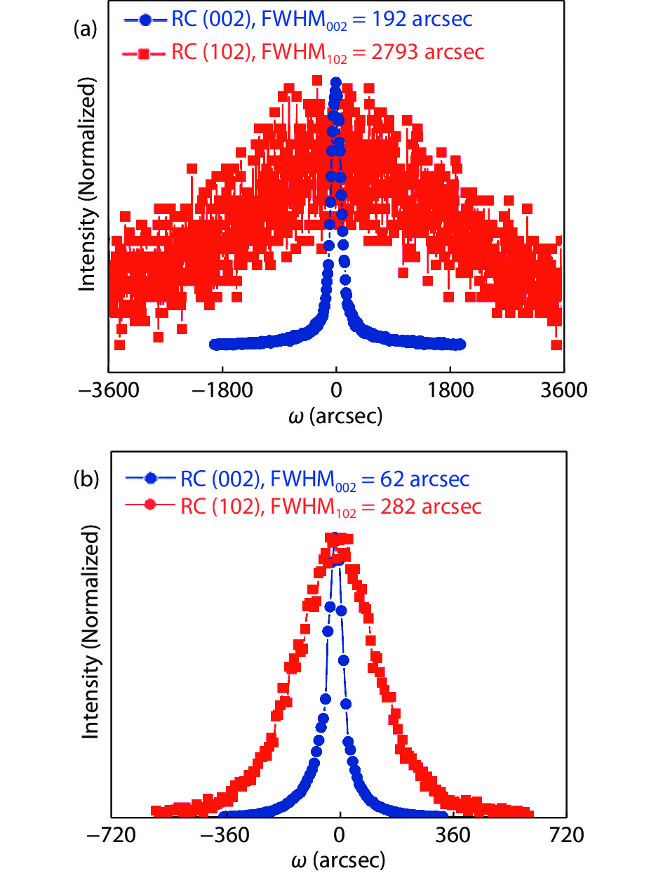
Fig. 1.
(Color online) The XRD rocking curves (XRC) of (002) (circles) and (102) (squares) planes for (a) as-sputtered and (b) HTA AlN samples.
ARTICLES
Shangfeng Liu1, 2, Ye Yuan2, , Shanshan Sheng1, Tao Wang4, Jin Zhang2, Lijie Huang2, Xiaohu Zhang2, Junjie Kang2, Wei Luo2, Yongde Li2, Houjin Wang2, Weiyun Wang2, Chuan Xiao2, Yaoping Liu2, Qi Wang3 and Xinqiang Wang1, 2,
Corresponding author: Ye Yuan, yuanye@sslab.org.cn; Xinqiang Wang, wangshi@pku.edu.cn
Abstract: In this work, based on physical vapor deposition and high-temperature annealing (HTA), the 4-inch crack-free high-quality AlN template is initialized. Benefiting from the crystal recrystallization during the HTA process, the FWHMs of X-ray rocking curves for (002) and (102) planes are encouragingly decreased to 62 and 282 arcsec, respectively. On such an AlN template, an ultra-thin AlN with a thickness of ~700 nm grown by MOCVD shows good quality, thus avoiding the epitaxial lateral overgrowth (ELOG) process in which 3–4 μm AlN is essential to obtain the flat surface and high crystalline quality. The 4-inch scaled wafer provides an avenue to match UVC-LED with the fabrication process of traditional GaN-based blue LED, therefore significantly improving yields and decreasing cost.
Key words: AlN, high temperature annealing, MOCVD
| [1] |
Hamzavi I H, Lyons A B, Kohli I, et al. Ultraviolet germicidal irradiation: Possible method for respirator disinfection to facilitate reuse during the COVID-19 pandemic. J Am Acad Dermatol, 2020, 82, 1511 doi: 10.1016/j.jaad.2020.03.085
|
| [2] |
Torres A E, Lyons A B, Narla S, et al. Ultraviolet-C and other methods of decontamination of filtering facepiece N-95 respirators during the COVID-19 pandemic. Photochem Photobiol Sci, 2020, 19, 746 doi: 10.1039/D0PP00131G
|
| [3] |
Liu S F, Luo W, Li D, et al. Sec-eliminating the SARS-CoV-2 by AlGaN based high power deep ultraviolet light source. Adv Funct Mater, 2021, 31, 2008452 doi: 10.1002/adfm.202008452
|
| [4] |
Kashima Y, Maeda N, Matsuura E, et al. High external quantum efficiency (10%) AlGaN-based deep-ultraviolet light-emitting diodes achieved by using highly reflective photonic crystal on p-AlGaN contact layer. Appl Phys Express, 2018, 11, 012101 doi: 10.7567/APEX.11.012101
|
| [5] |
Wang D, Uesugi K, Xiao S Y, et al. Low dislocation density AlN on sapphire prepared by double sputtering and annealing. Appl Phys Express, 2020, 13, 095501 doi: 10.35848/1882-0786/ababec
|
| [6] |
Miyake H, Lin C H, Tokoro K, et al. Preparation of high-quality AlN on sapphire by high-temperature face-to-face annealing. J Cryst Growth, 2016, 456, 155 doi: 10.1016/j.jcrysgro.2016.08.028
|
| [7] |
Huang C Y, Wu P Y, Chang K S, et al. High-quality and highly-transparent AlN template on annealed sputter-deposited AlN buffer layer for deep ultra-violet light-emitting diodes. AIP Adv, 2017, 7, 055110 doi: 10.1063/1.4983708
|
| [8] |
Yoshizawa R, Miyake H, Hiramatsu K. Effect of thermal annealing on AlN films grown on sputtered AlN templates by metalorganic vapor phase epitaxy. Jpn J Appl Phys, 2018, 57, 01AD05 doi: 10.7567/JJAP.57.01AD05
|
| [9] |
Hakamata J, Kawase Y, Dong L, et al. Growth of high-quality AlN and AlGaN films on sputtered AlN/sapphire templates via high-temperature annealing. Phys Status Solidi B, 2018, 255, 1700506 doi: 10.1002/pssb.201700506
|
| [10] |
Uesugi K, Shojiki K, Tezen Y, et al. Suppression of dislocation-induced spiral hillocks in MOVPE-grown AlGaN on face-to-face annealed sputter-deposited AlN template. Appl Phys Lett, 2020, 116, 062101 doi: 10.1063/1.5141825
|
| [11] |
Susilo N, Ziffer E, Hagedorn S, et al. Improved performance of UVC-LEDs by combination of high-temperature annealing and epitaxially laterally overgrown AlN/sapphire. Photon Res, 2020, 8, 589 doi: 10.1364/PRJ.385275
|
| [12] |
Susilo N, Hagedorn S, Jaeger D, et al. AlGaN-based deep UV LEDs grown on sputtered and high temperature annealed AlN/sapphire. Appl Phys Lett, 2018, 112, 041110 doi: 10.1063/1.5010265
|
| [13] |
Hagedorn S, Walde S, Mogilatenko A, et al. Stabilization of sputtered AlN/sapphire templates during high temperature annealing. J Cryst Growth, 2019, 512, 142 doi: 10.1016/j.jcrysgro.2019.02.024
|
| [14] |
Xiao S Y, Suzuki R, Miyake H, et al. Improvement mechanism of sputtered AlN films by high-temperature annealing. J Cryst Growth, 2018, 502, 41 doi: 10.1016/j.jcrysgro.2018.09.002
|
| [15] |
Wang M X, Xu F J, Xie N, et al. High-temperature annealing induced evolution of strain in AlN epitaxial films grown on sapphire substrates. Appl Phys Lett, 2019, 114, 112105 doi: 10.1063/1.5087547
|
| [16] |
Gu W, Liu Z B, Guo Y N, et al. Comprehensive study of crystalline AlN/sapphire templates after high-temperature annealing with various sputtering conditions. J Semicond, 2020, 41, 122802 doi: 10.1088/1674-4926/41/12/122802
|
| [17] |
Metzger T, Höpler R, Born E, et al. Defect structure of epitaxial GaN films determined by transmission electron microscopy and triple-axis X-ray diffractometry. Philos Mag A, 1998, 77, 1013 doi: 10.1080/01418619808221225
|
| [18] |
Pantha B N, Dahal R, Nakarmi M L, et al. Correlation between optoelectronic and structural properties and epilayer thickness of AlN. Appl Phys Lett, 2007, 90, 241101 doi: 10.1063/1.2747662
|
| [19] |
Ayers J E. The measurement of threading dislocation densities in semiconductor crystals by X-ray diffraction. J Cryst Growth, 1994, 135, 71 doi: 10.1016/0022-0248(94)90727-7
|
| [20] |
Srikant V, Speck J S, Clarke D R. Mosaic structure in epitaxial thin films having large lattice mismatch. J Appl Phys, 1997, 82, 4286 doi: 10.1063/1.366235
|
| [21] |
Chierchia R, Böttcher T, Heinke H, et al. Microstructure of heteroepitaxial GaN revealed by X-ray diffraction. J Appl Phys, 2003, 93, 8918 doi: 10.1063/1.1571217
|
| [22] |
Heinke H, Kirchner V, Einfeldt S, et al. X-ray diffraction analysis of the defect structure in epitaxial GaN. Appl Phys Lett, 2000, 77, 2145 doi: 10.1063/1.1314877
|
| [23] |
Wang X Q, Che S B, Ishitani Y, et al. Threading dislocations in In-polar InN films and their effects on surface morphology and electrical properties. Appl Phys Lett, 2007, 90, 151901 doi: 10.1063/1.2720717
|
| [24] |
Hagedorn S, Walde S, Knauer A, et al. Status and prospects of AlN templates on sapphire for ultraviolet light-emitting diodes. Phys Status Solidi A, 2020, 217, 1901022 doi: 10.1002/pssa.201901022
|
| [25] |
Yim W M, Paff R J. Thermal expansion of AlN, sapphire, and silicon. J Appl Phys, 1974, 45, 1456 doi: 10.1063/1.1663432
|
| [26] |
Fukuyama H, Miyake H, Nishio G, et al. Impact of high-temperature annealing of AlN layer on sapphire and its thermodynamic principle. Jpn J Appl Phys, 2016, 55, 05FL02 doi: 10.7567/JJAP.55.05FL02
|
| [27] |
Akiyma T, Uchino M, Nakamura K, et al. Structural analysis of polarity inversion boundary in sputtered AlN films annealed under high temperatures. Jpn J Appl Phys, 2019, 58, SCCB30 doi: 10.7567/1347-4065/ab0d01
|
| [28] |
Kamohara T, Akiyama M, Ueno N, et al. Influence of sputtering pressure on polarity distribution of aluminum nitride thin films. Appl Phys Lett, 2006, 89, 243507 doi: 10.1063/1.2405849
|
| [29] |
Kaur J, Kuwano N, Jamaludin K R, et al. Electron microscopy analysis of microstructure of postannealed aluminum nitride template. Appl Phys Express, 2016, 9, 065502 doi: 10.7567/APEX.9.065502
|
| [30] |
Yoshikawa A, Nagatomi T, Morishita T, et al. High-quality AlN film grown on a nanosized concave-convex surface sapphire substrate by metalorganic vapor phase epitaxy. Appl Phys Lett, 2017, 111, 162102 doi: 10.1063/1.5008258
|
| [31] |
Hayashi Y, Tanigawa K, Uesugi K, et al. Curvature-controllable and crack-free AlN/sapphire templates fabricated by sputtering and high-temperature annealing. J Cryst Growth, 2019, 512, 131 doi: 10.1016/j.jcrysgro.2019.02.026
|
| [32] |
Ben J W, Sun X J, Jia Y P, et al. Defect evolution in AlN templates on PVD-AlN/sapphire substrates by thermal annealing. CrystEngComm, 2018, 20, 4623 doi: 10.1039/C8CE00770E
|
| [33] |
Uedono A, Shojiki K, Uesugi K, et al. Annealing behaviors of vacancy-type defects in AlN deposited by radio-frequency sputtering and metalorganic vapor phase epitaxy studied using monoenergetic positron beams. J Appl Phys, 2020, 128, 085704 doi: 10.1063/5.0015225
|
| [34] |
Uesugi K, Hayashi Y, Shojiki K, et al. Reduction of threading dislocation density and suppression of cracking in sputter-deposited AlN templates annealed at high temperatures. Appl Phys Express, 2019, 12, 065501 doi: 10.7567/1882-0786/ab1ab8
|
| [35] |
Uesugi K, Hayashi Y, Shojiki K, et al. Fabrication of AlN templates on SiC substrates by sputtering-deposition and high-temperature annealing. J Cryst Growth, 2019, 510, 13 doi: 10.1016/j.jcrysgro.2019.01.011
|
| [36] |
Shojiki K, Uesugi K, Kuboya S, et al. High-quality AlN template prepared by face-to-face annealing of sputtered AlN on sapphire. Phys Status Solidi B, 2021, 258, 2000352 doi: 10.1002/pssb.202000352
|
| [37] |
Bryan I, Bryan Z, Mita S, et al. Surface kinetics in AlN growth: A universal model for the control of surface morphology in III-nitrides. J Cryst Growth, 2016, 438, 81 doi: 10.1016/j.jcrysgro.2015.12.022
|
| [38] |
Okada N, Kato N, Sato S, et al. Growth of high-quality and crack free AlN layers on sapphire substrate by multi-growth mode modification. J Cryst Growth, 2007, 298, 349 doi: 10.1016/j.jcrysgro.2006.10.123
|
| [39] |
Banal R G, Akashi Y, Matsuda K, et al. Crack-free thick AlN films obtained by NH3Nitridation of sapphire substrates. Jpn J Appl Phys, 2013, 52, 08JB21 doi: 10.7567/JJAP.52.08JB21
|
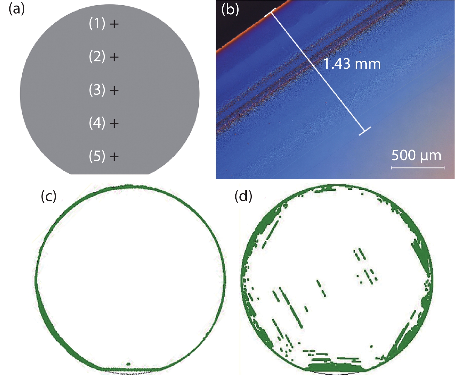
Table 1. Five points XRC FWHMs and θ–ω calculated strains of 4-inch post-HTA AlN and MOCVD regrown AlN wafers.
| Position | HTA AlN FWHM (002)/(102) (arcsec) | Regrown AlN FWHM (002)/(102) (arcsec) | Regrown AlN strain // c (%) |
| 1 | 87 / 310 | 162 / 381 | 0.0869 |
| 2 | 64 / 288 | 95 / 372 | 0.0799 |
| 3 | 57 / 283 | 85 / 320 | 0.0795 |
| 4 | 61 / 310 | 78 / 312 | 0.0795 |
| 5 | 70 / 321 | 89 / 329 | 0.0807 |
 DownLoad: CSV
| [1] |
Hamzavi I H, Lyons A B, Kohli I, et al. Ultraviolet germicidal irradiation: Possible method for respirator disinfection to facilitate reuse during the COVID-19 pandemic. J Am Acad Dermatol, 2020, 82, 1511 doi: 10.1016/j.jaad.2020.03.085
|
| [2] |
Torres A E, Lyons A B, Narla S, et al. Ultraviolet-C and other methods of decontamination of filtering facepiece N-95 respirators during the COVID-19 pandemic. Photochem Photobiol Sci, 2020, 19, 746 doi: 10.1039/D0PP00131G
|
| [3] |
Liu S F, Luo W, Li D, et al. Sec-eliminating the SARS-CoV-2 by AlGaN based high power deep ultraviolet light source. Adv Funct Mater, 2021, 31, 2008452 doi: 10.1002/adfm.202008452
|
| [4] |
Kashima Y, Maeda N, Matsuura E, et al. High external quantum efficiency (10%) AlGaN-based deep-ultraviolet light-emitting diodes achieved by using highly reflective photonic crystal on p-AlGaN contact layer. Appl Phys Express, 2018, 11, 012101 doi: 10.7567/APEX.11.012101
|
| [5] |
Wang D, Uesugi K, Xiao S Y, et al. Low dislocation density AlN on sapphire prepared by double sputtering and annealing. Appl Phys Express, 2020, 13, 095501 doi: 10.35848/1882-0786/ababec
|
| [6] |
Miyake H, Lin C H, Tokoro K, et al. Preparation of high-quality AlN on sapphire by high-temperature face-to-face annealing. J Cryst Growth, 2016, 456, 155 doi: 10.1016/j.jcrysgro.2016.08.028
|
| [7] |
Huang C Y, Wu P Y, Chang K S, et al. High-quality and highly-transparent AlN template on annealed sputter-deposited AlN buffer layer for deep ultra-violet light-emitting diodes. AIP Adv, 2017, 7, 055110 doi: 10.1063/1.4983708
|
| [8] |
Yoshizawa R, Miyake H, Hiramatsu K. Effect of thermal annealing on AlN films grown on sputtered AlN templates by metalorganic vapor phase epitaxy. Jpn J Appl Phys, 2018, 57, 01AD05 doi: 10.7567/JJAP.57.01AD05
|
| [9] |
Hakamata J, Kawase Y, Dong L, et al. Growth of high-quality AlN and AlGaN films on sputtered AlN/sapphire templates via high-temperature annealing. Phys Status Solidi B, 2018, 255, 1700506 doi: 10.1002/pssb.201700506
|
| [10] |
Uesugi K, Shojiki K, Tezen Y, et al. Suppression of dislocation-induced spiral hillocks in MOVPE-grown AlGaN on face-to-face annealed sputter-deposited AlN template. Appl Phys Lett, 2020, 116, 062101 doi: 10.1063/1.5141825
|
| [11] |
Susilo N, Ziffer E, Hagedorn S, et al. Improved performance of UVC-LEDs by combination of high-temperature annealing and epitaxially laterally overgrown AlN/sapphire. Photon Res, 2020, 8, 589 doi: 10.1364/PRJ.385275
|
| [12] |
Susilo N, Hagedorn S, Jaeger D, et al. AlGaN-based deep UV LEDs grown on sputtered and high temperature annealed AlN/sapphire. Appl Phys Lett, 2018, 112, 041110 doi: 10.1063/1.5010265
|
| [13] |
Hagedorn S, Walde S, Mogilatenko A, et al. Stabilization of sputtered AlN/sapphire templates during high temperature annealing. J Cryst Growth, 2019, 512, 142 doi: 10.1016/j.jcrysgro.2019.02.024
|
| [14] |
Xiao S Y, Suzuki R, Miyake H, et al. Improvement mechanism of sputtered AlN films by high-temperature annealing. J Cryst Growth, 2018, 502, 41 doi: 10.1016/j.jcrysgro.2018.09.002
|
| [15] |
Wang M X, Xu F J, Xie N, et al. High-temperature annealing induced evolution of strain in AlN epitaxial films grown on sapphire substrates. Appl Phys Lett, 2019, 114, 112105 doi: 10.1063/1.5087547
|
| [16] |
Gu W, Liu Z B, Guo Y N, et al. Comprehensive study of crystalline AlN/sapphire templates after high-temperature annealing with various sputtering conditions. J Semicond, 2020, 41, 122802 doi: 10.1088/1674-4926/41/12/122802
|
| [17] |
Metzger T, Höpler R, Born E, et al. Defect structure of epitaxial GaN films determined by transmission electron microscopy and triple-axis X-ray diffractometry. Philos Mag A, 1998, 77, 1013 doi: 10.1080/01418619808221225
|
| [18] |
Pantha B N, Dahal R, Nakarmi M L, et al. Correlation between optoelectronic and structural properties and epilayer thickness of AlN. Appl Phys Lett, 2007, 90, 241101 doi: 10.1063/1.2747662
|
| [19] |
Ayers J E. The measurement of threading dislocation densities in semiconductor crystals by X-ray diffraction. J Cryst Growth, 1994, 135, 71 doi: 10.1016/0022-0248(94)90727-7
|
| [20] |
Srikant V, Speck J S, Clarke D R. Mosaic structure in epitaxial thin films having large lattice mismatch. J Appl Phys, 1997, 82, 4286 doi: 10.1063/1.366235
|
| [21] |
Chierchia R, Böttcher T, Heinke H, et al. Microstructure of heteroepitaxial GaN revealed by X-ray diffraction. J Appl Phys, 2003, 93, 8918 doi: 10.1063/1.1571217
|
| [22] |
Heinke H, Kirchner V, Einfeldt S, et al. X-ray diffraction analysis of the defect structure in epitaxial GaN. Appl Phys Lett, 2000, 77, 2145 doi: 10.1063/1.1314877
|
| [23] |
Wang X Q, Che S B, Ishitani Y, et al. Threading dislocations in In-polar InN films and their effects on surface morphology and electrical properties. Appl Phys Lett, 2007, 90, 151901 doi: 10.1063/1.2720717
|
| [24] |
Hagedorn S, Walde S, Knauer A, et al. Status and prospects of AlN templates on sapphire for ultraviolet light-emitting diodes. Phys Status Solidi A, 2020, 217, 1901022 doi: 10.1002/pssa.201901022
|
| [25] |
Yim W M, Paff R J. Thermal expansion of AlN, sapphire, and silicon. J Appl Phys, 1974, 45, 1456 doi: 10.1063/1.1663432
|
| [26] |
Fukuyama H, Miyake H, Nishio G, et al. Impact of high-temperature annealing of AlN layer on sapphire and its thermodynamic principle. Jpn J Appl Phys, 2016, 55, 05FL02 doi: 10.7567/JJAP.55.05FL02
|
| [27] |
Akiyma T, Uchino M, Nakamura K, et al. Structural analysis of polarity inversion boundary in sputtered AlN films annealed under high temperatures. Jpn J Appl Phys, 2019, 58, SCCB30 doi: 10.7567/1347-4065/ab0d01
|
| [28] |
Kamohara T, Akiyama M, Ueno N, et al. Influence of sputtering pressure on polarity distribution of aluminum nitride thin films. Appl Phys Lett, 2006, 89, 243507 doi: 10.1063/1.2405849
|
| [29] |
Kaur J, Kuwano N, Jamaludin K R, et al. Electron microscopy analysis of microstructure of postannealed aluminum nitride template. Appl Phys Express, 2016, 9, 065502 doi: 10.7567/APEX.9.065502
|
| [30] |
Yoshikawa A, Nagatomi T, Morishita T, et al. High-quality AlN film grown on a nanosized concave-convex surface sapphire substrate by metalorganic vapor phase epitaxy. Appl Phys Lett, 2017, 111, 162102 doi: 10.1063/1.5008258
|
| [31] |
Hayashi Y, Tanigawa K, Uesugi K, et al. Curvature-controllable and crack-free AlN/sapphire templates fabricated by sputtering and high-temperature annealing. J Cryst Growth, 2019, 512, 131 doi: 10.1016/j.jcrysgro.2019.02.026
|
| [32] |
Ben J W, Sun X J, Jia Y P, et al. Defect evolution in AlN templates on PVD-AlN/sapphire substrates by thermal annealing. CrystEngComm, 2018, 20, 4623 doi: 10.1039/C8CE00770E
|
| [33] |
Uedono A, Shojiki K, Uesugi K, et al. Annealing behaviors of vacancy-type defects in AlN deposited by radio-frequency sputtering and metalorganic vapor phase epitaxy studied using monoenergetic positron beams. J Appl Phys, 2020, 128, 085704 doi: 10.1063/5.0015225
|
| [34] |
Uesugi K, Hayashi Y, Shojiki K, et al. Reduction of threading dislocation density and suppression of cracking in sputter-deposited AlN templates annealed at high temperatures. Appl Phys Express, 2019, 12, 065501 doi: 10.7567/1882-0786/ab1ab8
|
| [35] |
Uesugi K, Hayashi Y, Shojiki K, et al. Fabrication of AlN templates on SiC substrates by sputtering-deposition and high-temperature annealing. J Cryst Growth, 2019, 510, 13 doi: 10.1016/j.jcrysgro.2019.01.011
|
| [36] |
Shojiki K, Uesugi K, Kuboya S, et al. High-quality AlN template prepared by face-to-face annealing of sputtered AlN on sapphire. Phys Status Solidi B, 2021, 258, 2000352 doi: 10.1002/pssb.202000352
|
| [37] |
Bryan I, Bryan Z, Mita S, et al. Surface kinetics in AlN growth: A universal model for the control of surface morphology in III-nitrides. J Cryst Growth, 2016, 438, 81 doi: 10.1016/j.jcrysgro.2015.12.022
|
| [38] |
Okada N, Kato N, Sato S, et al. Growth of high-quality and crack free AlN layers on sapphire substrate by multi-growth mode modification. J Cryst Growth, 2007, 298, 349 doi: 10.1016/j.jcrysgro.2006.10.123
|
| [39] |
Banal R G, Akashi Y, Matsuda K, et al. Crack-free thick AlN films obtained by NH3Nitridation of sapphire substrates. Jpn J Appl Phys, 2013, 52, 08JB21 doi: 10.7567/JJAP.52.08JB21
|


Article views: 2355 Times PDF downloads: 167 Times Cited by: 0 Times
Received: 28 July 2021 Revised: 07 September 2021 Online: Accepted Manuscript: 26 October 2021Uncorrected proof: 01 November 2021Published: 03 December 2021
| Citation: |
Shangfeng Liu, Ye Yuan, Shanshan Sheng, Tao Wang, Jin Zhang, Lijie Huang, Xiaohu Zhang, Junjie Kang, Wei Luo, Yongde Li, Houjin Wang, Weiyun Wang, Chuan Xiao, Yaoping Liu, Qi Wang, Xinqiang Wang. Four-inch high quality crack-free AlN layer grown on a high-temperature annealed AlN template by MOCVD[J]. Journal of Semiconductors, 2021, 42(12): 122804. doi: 10.1088/1674-4926/42/12/122804
S F Liu, Y Yuan, S S Sheng, T Wang, J Zhang, L J Huang, X H Zhang, J J Kang, W Luo, Y D Li, H J Wang, W Y Wang, C Xiao, Y P Liu, Q Wang, X Q Wang, Four-inch high quality crack-free AlN layer grown on a high-temperature annealed AlN template by MOCVD[J]. J. Semicond., 2021, 42(12): 122804. doi: 10.1088/1674-4926/42/12/122804.
Export: BibTex EndNote

|
| [1] |
Hamzavi I H, Lyons A B, Kohli I, et al. Ultraviolet germicidal irradiation: Possible method for respirator disinfection to facilitate reuse during the COVID-19 pandemic. J Am Acad Dermatol, 2020, 82, 1511 doi: 10.1016/j.jaad.2020.03.085
|
| [2] |
Torres A E, Lyons A B, Narla S, et al. Ultraviolet-C and other methods of decontamination of filtering facepiece N-95 respirators during the COVID-19 pandemic. Photochem Photobiol Sci, 2020, 19, 746 doi: 10.1039/D0PP00131G
|
| [3] |
Liu S F, Luo W, Li D, et al. Sec-eliminating the SARS-CoV-2 by AlGaN based high power deep ultraviolet light source. Adv Funct Mater, 2021, 31, 2008452 doi: 10.1002/adfm.202008452
|
| [4] |
Kashima Y, Maeda N, Matsuura E, et al. High external quantum efficiency (10%) AlGaN-based deep-ultraviolet light-emitting diodes achieved by using highly reflective photonic crystal on p-AlGaN contact layer. Appl Phys Express, 2018, 11, 012101 doi: 10.7567/APEX.11.012101
|
| [5] |
Wang D, Uesugi K, Xiao S Y, et al. Low dislocation density AlN on sapphire prepared by double sputtering and annealing. Appl Phys Express, 2020, 13, 095501 doi: 10.35848/1882-0786/ababec
|
| [6] |
Miyake H, Lin C H, Tokoro K, et al. Preparation of high-quality AlN on sapphire by high-temperature face-to-face annealing. J Cryst Growth, 2016, 456, 155 doi: 10.1016/j.jcrysgro.2016.08.028
|
| [7] |
Huang C Y, Wu P Y, Chang K S, et al. High-quality and highly-transparent AlN template on annealed sputter-deposited AlN buffer layer for deep ultra-violet light-emitting diodes. AIP Adv, 2017, 7, 055110 doi: 10.1063/1.4983708
|
| [8] |
Yoshizawa R, Miyake H, Hiramatsu K. Effect of thermal annealing on AlN films grown on sputtered AlN templates by metalorganic vapor phase epitaxy. Jpn J Appl Phys, 2018, 57, 01AD05 doi: 10.7567/JJAP.57.01AD05
|
| [9] |
Hakamata J, Kawase Y, Dong L, et al. Growth of high-quality AlN and AlGaN films on sputtered AlN/sapphire templates via high-temperature annealing. Phys Status Solidi B, 2018, 255, 1700506 doi: 10.1002/pssb.201700506
|
| [10] |
Uesugi K, Shojiki K, Tezen Y, et al. Suppression of dislocation-induced spiral hillocks in MOVPE-grown AlGaN on face-to-face annealed sputter-deposited AlN template. Appl Phys Lett, 2020, 116, 062101 doi: 10.1063/1.5141825
|
| [11] |
Susilo N, Ziffer E, Hagedorn S, et al. Improved performance of UVC-LEDs by combination of high-temperature annealing and epitaxially laterally overgrown AlN/sapphire. Photon Res, 2020, 8, 589 doi: 10.1364/PRJ.385275
|
| [12] |
Susilo N, Hagedorn S, Jaeger D, et al. AlGaN-based deep UV LEDs grown on sputtered and high temperature annealed AlN/sapphire. Appl Phys Lett, 2018, 112, 041110 doi: 10.1063/1.5010265
|
| [13] |
Hagedorn S, Walde S, Mogilatenko A, et al. Stabilization of sputtered AlN/sapphire templates during high temperature annealing. J Cryst Growth, 2019, 512, 142 doi: 10.1016/j.jcrysgro.2019.02.024
|
| [14] |
Xiao S Y, Suzuki R, Miyake H, et al. Improvement mechanism of sputtered AlN films by high-temperature annealing. J Cryst Growth, 2018, 502, 41 doi: 10.1016/j.jcrysgro.2018.09.002
|
| [15] |
Wang M X, Xu F J, Xie N, et al. High-temperature annealing induced evolution of strain in AlN epitaxial films grown on sapphire substrates. Appl Phys Lett, 2019, 114, 112105 doi: 10.1063/1.5087547
|
| [16] |
Gu W, Liu Z B, Guo Y N, et al. Comprehensive study of crystalline AlN/sapphire templates after high-temperature annealing with various sputtering conditions. J Semicond, 2020, 41, 122802 doi: 10.1088/1674-4926/41/12/122802
|
| [17] |
Metzger T, Höpler R, Born E, et al. Defect structure of epitaxial GaN films determined by transmission electron microscopy and triple-axis X-ray diffractometry. Philos Mag A, 1998, 77, 1013 doi: 10.1080/01418619808221225
|
| [18] |
Pantha B N, Dahal R, Nakarmi M L, et al. Correlation between optoelectronic and structural properties and epilayer thickness of AlN. Appl Phys Lett, 2007, 90, 241101 doi: 10.1063/1.2747662
|
| [19] |
Ayers J E. The measurement of threading dislocation densities in semiconductor crystals by X-ray diffraction. J Cryst Growth, 1994, 135, 71 doi: 10.1016/0022-0248(94)90727-7
|
| [20] |
Srikant V, Speck J S, Clarke D R. Mosaic structure in epitaxial thin films having large lattice mismatch. J Appl Phys, 1997, 82, 4286 doi: 10.1063/1.366235
|
| [21] |
Chierchia R, Böttcher T, Heinke H, et al. Microstructure of heteroepitaxial GaN revealed by X-ray diffraction. J Appl Phys, 2003, 93, 8918 doi: 10.1063/1.1571217
|
| [22] |
Heinke H, Kirchner V, Einfeldt S, et al. X-ray diffraction analysis of the defect structure in epitaxial GaN. Appl Phys Lett, 2000, 77, 2145 doi: 10.1063/1.1314877
|
| [23] |
Wang X Q, Che S B, Ishitani Y, et al. Threading dislocations in In-polar InN films and their effects on surface morphology and electrical properties. Appl Phys Lett, 2007, 90, 151901 doi: 10.1063/1.2720717
|
| [24] |
Hagedorn S, Walde S, Knauer A, et al. Status and prospects of AlN templates on sapphire for ultraviolet light-emitting diodes. Phys Status Solidi A, 2020, 217, 1901022 doi: 10.1002/pssa.201901022
|
| [25] |
Yim W M, Paff R J. Thermal expansion of AlN, sapphire, and silicon. J Appl Phys, 1974, 45, 1456 doi: 10.1063/1.1663432
|
| [26] |
Fukuyama H, Miyake H, Nishio G, et al. Impact of high-temperature annealing of AlN layer on sapphire and its thermodynamic principle. Jpn J Appl Phys, 2016, 55, 05FL02 doi: 10.7567/JJAP.55.05FL02
|
| [27] |
Akiyma T, Uchino M, Nakamura K, et al. Structural analysis of polarity inversion boundary in sputtered AlN films annealed under high temperatures. Jpn J Appl Phys, 2019, 58, SCCB30 doi: 10.7567/1347-4065/ab0d01
|
| [28] |
Kamohara T, Akiyama M, Ueno N, et al. Influence of sputtering pressure on polarity distribution of aluminum nitride thin films. Appl Phys Lett, 2006, 89, 243507 doi: 10.1063/1.2405849
|
| [29] |
Kaur J, Kuwano N, Jamaludin K R, et al. Electron microscopy analysis of microstructure of postannealed aluminum nitride template. Appl Phys Express, 2016, 9, 065502 doi: 10.7567/APEX.9.065502
|
| [30] |
Yoshikawa A, Nagatomi T, Morishita T, et al. High-quality AlN film grown on a nanosized concave-convex surface sapphire substrate by metalorganic vapor phase epitaxy. Appl Phys Lett, 2017, 111, 162102 doi: 10.1063/1.5008258
|
| [31] |
Hayashi Y, Tanigawa K, Uesugi K, et al. Curvature-controllable and crack-free AlN/sapphire templates fabricated by sputtering and high-temperature annealing. J Cryst Growth, 2019, 512, 131 doi: 10.1016/j.jcrysgro.2019.02.026
|
| [32] |
Ben J W, Sun X J, Jia Y P, et al. Defect evolution in AlN templates on PVD-AlN/sapphire substrates by thermal annealing. CrystEngComm, 2018, 20, 4623 doi: 10.1039/C8CE00770E
|
| [33] |
Uedono A, Shojiki K, Uesugi K, et al. Annealing behaviors of vacancy-type defects in AlN deposited by radio-frequency sputtering and metalorganic vapor phase epitaxy studied using monoenergetic positron beams. J Appl Phys, 2020, 128, 085704 doi: 10.1063/5.0015225
|
| [34] |
Uesugi K, Hayashi Y, Shojiki K, et al. Reduction of threading dislocation density and suppression of cracking in sputter-deposited AlN templates annealed at high temperatures. Appl Phys Express, 2019, 12, 065501 doi: 10.7567/1882-0786/ab1ab8
|
| [35] |
Uesugi K, Hayashi Y, Shojiki K, et al. Fabrication of AlN templates on SiC substrates by sputtering-deposition and high-temperature annealing. J Cryst Growth, 2019, 510, 13 doi: 10.1016/j.jcrysgro.2019.01.011
|
| [36] |
Shojiki K, Uesugi K, Kuboya S, et al. High-quality AlN template prepared by face-to-face annealing of sputtered AlN on sapphire. Phys Status Solidi B, 2021, 258, 2000352 doi: 10.1002/pssb.202000352
|
| [37] |
Bryan I, Bryan Z, Mita S, et al. Surface kinetics in AlN growth: A universal model for the control of surface morphology in III-nitrides. J Cryst Growth, 2016, 438, 81 doi: 10.1016/j.jcrysgro.2015.12.022
|
| [38] |
Okada N, Kato N, Sato S, et al. Growth of high-quality and crack free AlN layers on sapphire substrate by multi-growth mode modification. J Cryst Growth, 2007, 298, 349 doi: 10.1016/j.jcrysgro.2006.10.123
|
| [39] |
Banal R G, Akashi Y, Matsuda K, et al. Crack-free thick AlN films obtained by NH3Nitridation of sapphire substrates. Jpn J Appl Phys, 2013, 52, 08JB21 doi: 10.7567/JJAP.52.08JB21
|

 WeChat ID
Journal of Semiconductors © 2017 All Rights Reserved 京ICP备05085259号-2


