ARTICLES

Low-thermal-budget Au-free ohmic contact to an ultrathin barrier AlGaN/GaN heterostructure utilizing a micro-patterned ohmic recess

Wen Shi1, 2, Sen Huang1, 2, , Xinhua Wang1, 2, , Qimeng Jiang1, 2, Yixu Yao1, 2, Lan Bi1, 2, Yuchen Li1, 2, Kexin Deng1, 2, Jie Fan1, 2, Haibo Yin1, 2, Ke Wei1, 2, Yankui Li1, 2, Jingyuan Shi1, 2, Haojie Jiang1, 2, Junfeng Li1, 2 and Xinyu Liu1, 2,

+ Author Affiliations

 Corresponding author: Sen Huang, huangsen@ime.ac.cn; Xinhua Wang, wangxinhua@ime.ac.cn; Xinyu Liu, xyliu@ime.ac.cn

PDF

Turn off MathJax

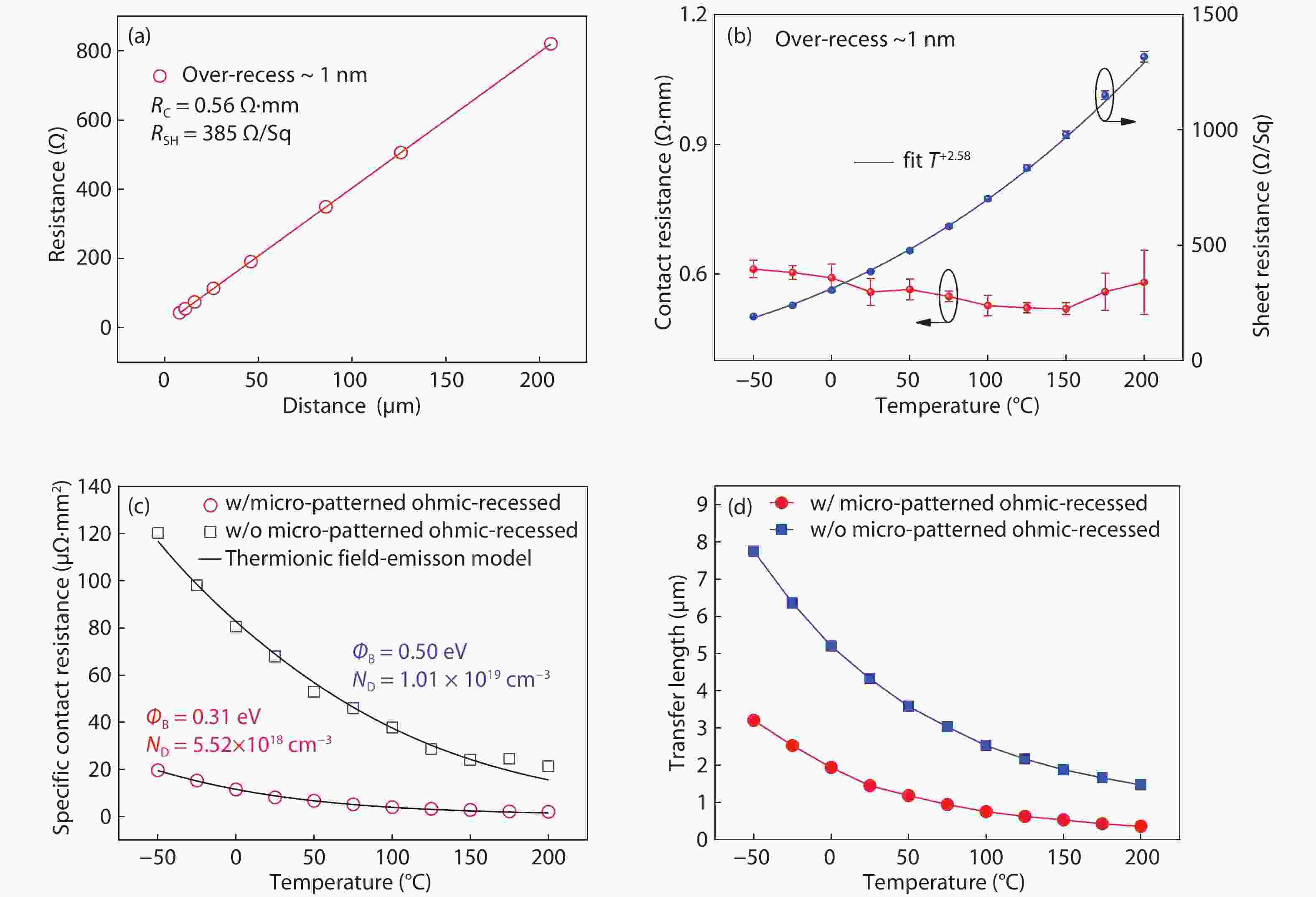
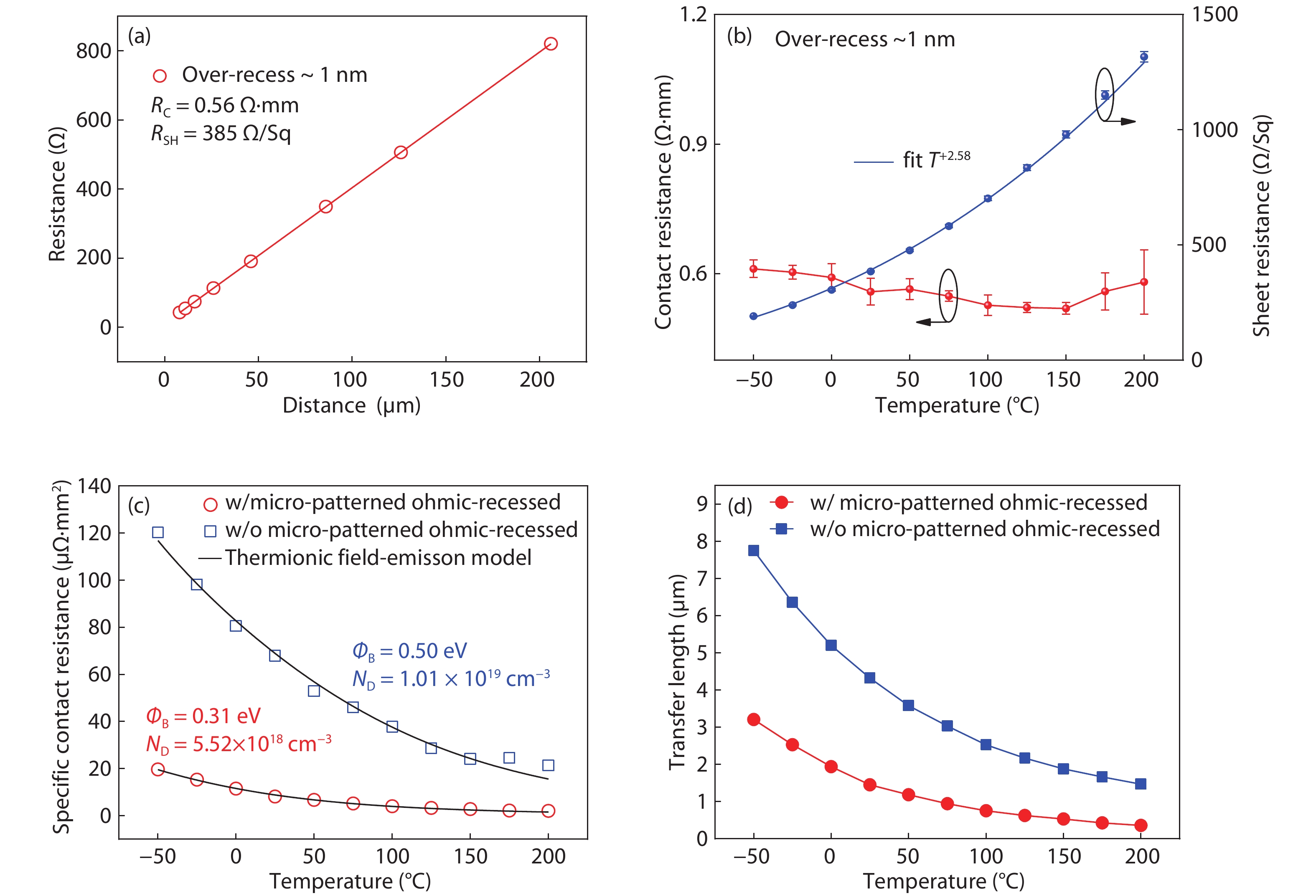
Abstract: A pre-ohmic micro-patterned recess process, is utilized to fabricate Ti/Al/Ti/TiN ohmic contact to an ultrathin-barrier (UTB) AlGaN/GaN heterostructure, featuring a significantly reduced ohmic contact resistivity of 0.56 Ω·mm at an alloy temperature of 550 °C. The sheet resistances increase with the temperature following a power law with the index of +2.58, while the specific contact resistivity decreases with the temperature. The contact mechanism can be well described by thermionic field emission (TFE). The extracted Schottky barrier height and electron concentration are 0.31 eV and 5.52 × 1018 cm−3, which suggests an intimate contact between ohmic metal and the UTB-AlGaN as well as GaN buffer. A good correlation between ohmic transfer length and the micro-pattern size is revealed, though in-depth investigation is needed. A preliminary CMOS-process-compatible metal–insulator–semiconductor high-mobility transistor (MIS-HEMT) was fabricated with the proposed Au-free ohmic contact technique.

Key words: ultrathin-barrier AlGaN/GaN heterostructurelow thermal budgetAu-free ohmic contactmicro-patterned ohmic recessMIS-HEMTstransfer length


[1]
Huang S, Liu X Y, Wang X H, et al. Ultrathin-barrier AlGaN/GaN heterostructure: A recess-free technology for manufacturing high-performance GaN-on-Si power devices. IEEE Trans Electron Devices, 2018, 65, 207 doi: 10.1109/TED.2017.2773201
[2]
Jiang H X, Tang C W, Lau K M. Enhancement-mode GaN MOS-HEMTs with recess-free barrier engineering and high-k ZrO2 gate dielectric. IEEE Electron Device Lett, 2018, 39, 405 doi: 10.1109/LED.2018.2792839
[3]
Han P C, Yan Z Z, Wu C H, et al. Recess-free normally-off GaN MIS-HEMT fabricated on ultra-thin-barrier AlGaN/GaN heterostructure. 2019 31st International Symposium on Power Semiconductor Devices and ICs (ISPSD), 2019, 427
[4]
Huang S, Wang X H, Liu X Y, et al. Monolithic integration of E/D-mode GaN MIS-HEMTs on ultrathin-barrier AlGaN/GaN heterostructure on Si substrates. Appl Phys Express, 2019, 12, 024001 doi: 10.7567/1882-0786/aafa0e
[5]
Peralagu U, Alian A, Putcha V, et al. CMOS-compatible GaN-based devices on 200mm-Si for RF applications: Integration and Performance. 2019 IEEE International Electron Devices Meeting (IEDM), 2019, 17.2.1
[6]
Then H W, Dasgupta S, Radosavljevic M, et al. 3D heterogeneous integration of high performance high-K metal gate GaN NMOS and Si PMOS transistors on 300mm high-resistivity Si substrate for energy-efficient and compact power delivery, RF (5G and beyond) and SoC applications. 2019 IEEE International Electron Devices Meeting (IEDM), 2019, 17.3.1
[7]
Marcon D, De Jaeger B, Halder S, et al. Manufacturing challenges of GaN-on-Si HEMTs in a 200 mm CMOS fab. IEEE Trans Semicond Manuf, 2013, 26, 361 doi: 10.1109/TSM.2013.2255897
[8]
Lee H S, Lee D S, Palacios T. AlGaN/GaN high-electron-mobility transistors fabricated through a Au-free technology. IEEE Electron Device Lett, 2011, 32, 623 doi: 10.1109/LED.2011.2114322
[9]
Li Y, Ng G I, Arulkumaran S, et al. Conduction mechanism of non-gold Ta/Si/Ti/Al/Ni/Ta ohmic contacts in AlGaN/GaN high-electron-mobility transistors. Appl Phys Express, 2015, 8, 041001 doi: 10.7567/APEX.8.041001
[10]
Zhang J H, Huang S, Bao Q L, et al. Mechanism of Ti/Al/Ti/W Au-free ohmic contacts to AlGaN/GaN heterostructures via pre-ohmic recess etching and low temperature annealing. Appl Phys Lett, 2015, 107, 262109 doi: 10.1063/1.4939190
[11]
Shriki A, Winter R, Calahorra Y, et al. Formation mechanism of gold-based and gold-free ohmic contacts to AlGaN/GaN heterostructure field effect transistors. J Appl Phys, 2017, 121, 065301 doi: 10.1063/1.4975473
[12]
Yoshida T, Egawa T. Improvement of Au-free, Ti/Al/W ohmic contact on AlGaN/GaN heterostructure featuring a thin-Ti layer and low temperature annealing. Phys Status Solidi A, 2018, 215, 1700825 doi: 10.1002/pssa.201700825
[13]
Zhang J H, Kang X W, Wang X H, et al. Ultralow-contact-resistance Au-free ohmic contacts with low annealing temperature on AlGaN/GaN heterostructures. IEEE Electron Device Lett, 2018, 39, 847 doi: 10.1109/LED.2018.2822659
[14]
Fan M Y, Yang G Y, Zhou G N, et al. Ultra-low contact resistivity of < 0.1 Ω mm for Au-free TixAly alloy contact on non-recessed i-AlGaN/GaN. IEEE Electron Device Lett, 2020, 41, 143 doi: 10.1109/LED.2019.2953077
[15]
Ma X H, Liu Y, Wang X H, et al. Effect of alloying temperature on the capacitance-voltage and current-voltage characteristics of low-pressure chemical vapor deposition SiNx/n-GaN MIS structures. Phys Status Solidi A, 2015, 212, 2928 doi: 10.1002/pssa.201532395
[16]
Wang Y K, Huang S, Wang X H, et al. Effects of fluorine plasma treatment on Au-free ohmic contacts to ultrathin-barrier AlGaN/GaN heterostructure. IEEE Trans Electron Devices, 2019, 66, 2932 doi: 10.1109/TED.2019.2916997
[17]
Guo J, Li G W, Faria F, et al. MBE-regrown ohmics in InAlN HEMTs with a regrowth interface resistance of 0.05 Ω mm. IEEE Electron Device Lett, 2012, 33, 525 doi: 10.1109/LED.2012.2186116
[18]
Huang T D, Zhu X L, Lau K M. Enhancement-mode AlN/GaN MOSHFETs on Si substrate with regrown source/drain by MOCVD. IEEE Electron Device Lett, 2012, 33, 1123 doi: 10.1109/LED.2012.2198911
[19]
Yu H J, McCarthy L, Rajan S, et al. Ion implanted AlGaN-GaN HEMTs with nonalloyed Ohmic contacts. IEEE Electron Device Lett, 2005, 26, 283 doi: 10.1109/LED.2005.846583
[20]
Lu Y, Ma X H, Yang L, et al. High RF performance AlGaN/GaN HEMT fabricated by recess-arrayed ohmic contact technology. IEEE Electron Device Lett, 2018, 39, 811 doi: 10.1109/LED.2018.2828860
[21]
Benakaprasad B, Eblabla A M, Li X, et al. Optimization of ohmic contact for AlGaN/GaN HEMT on low-resistivity silicon. IEEE Trans Electron Devices, 2020, 67, 863 doi: 10.1109/TED.2020.2968186
[22]
Antoszewski J, Gracey M, Dell J M, et al. Scattering mechanisms limiting two-dimensional electron gas mobility in Al0.25Ga0.75N/GaN modulation-doped field-effect transistors. J Appl Phys, 2000, 87, 3900 doi: 10.1063/1.372432
[23]
Liu Z H, Arulkumaran S, Ng G I. Temperature dependence of Ohmic contact characteristics in AlGaN/GaN high electron mobility transistors from −50 to 200 °C. Appl Phys Lett, 2009, 94, 142105 doi: 10.1063/1.3114422
[24]
Aminbeidokhti A, Dimitrijev S, Han J S, et al. The power law of phonon-limited electron mobility in the 2-D electron gas of AlGaN/GaN heterostructure. IEEE Trans Electron Devices, 2016, 63, 2214 doi: 10.1109/TED.2016.2544920
[25]
Iucolano F, Greco G, Roccaforte F. Correlation between microstructure and temperature dependent electrical behavior of annealed Ti/Al/Ni/Au Ohmic contacts to AlGaN/GaN heterostructures. Appl Phys Lett, 2013, 103, 201604 doi: 10.1063/1.4828839
[26]
Iucolano F, Roccaforte F, Alberti A, et al. Temperature dependence of the specific resistance in Ti/Al/Ni/Au contacts on n-type GaN. J Appl Phys, 2006, 100, 123706 doi: 10.1063/1.2400825
[27]
Takei Y, Kamiya M, Tsutsui K, et al. Reduction of contact resistance on AlGaN/GaN HEMT structures introducing uneven AlGaN layers. Phys Status Solidi A, 2015, 212, 1104 doi: 10.1002/pssa.201431645
Fig. 1.  (Color online) (a) Schematic cross section of the fabricated Si-CMOS-compatible GaN MIS-HEMTs utilizing a micro-patterned ohmic recess. (b) SEM image. (c) Line profile of the micro-patterned AlGaN/GaN heterostructure measured by atomic force microscopy (AFM).

Fig. 2.  (a) Linear fit of the fabricated Ti/Al/Ti/TiN ohmic contact resistances versus TLM spacing. (b) Temperature-dependent characteristics: RC and RSH. (c) ρC as fitted by thermionic field emission model. (d) Temperature-dependent transfer length LT.

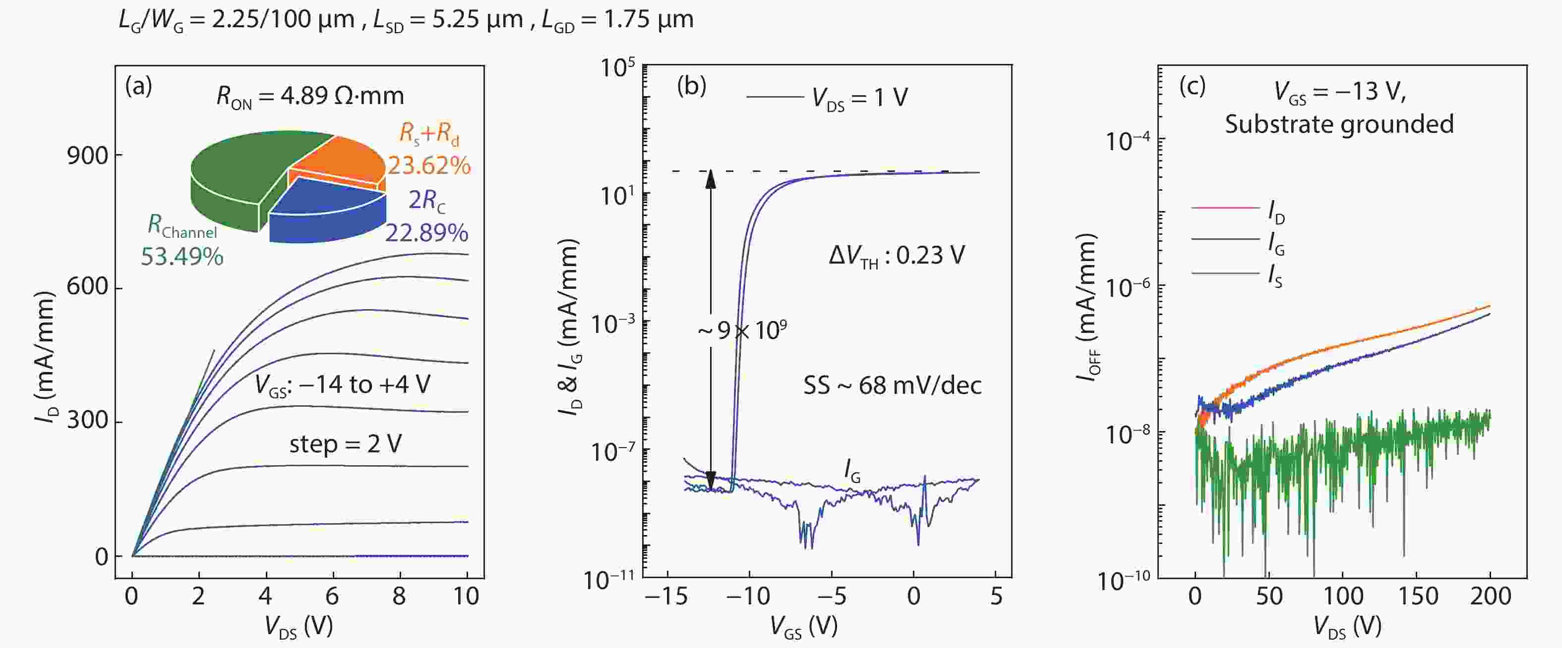
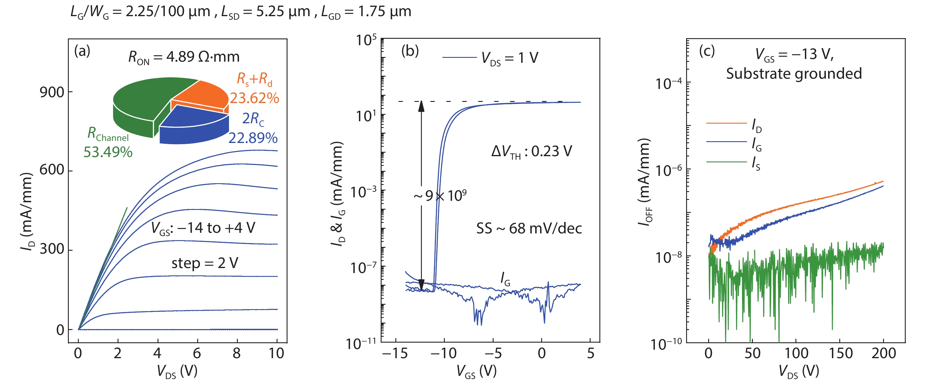
Fig. 3.  (Color online) (a) DC output, (b) transfer, and (c) off-state leakage characteristics of the fabricated CMOS-process compatible LPCVD-SiNx/AlGaN/GaN MIS-HEMTs.

Table 1.   The summary of micro-patterned ohmic contacts to various AlGaN/GaN heterostructures.

AlGaN/GaN heterostructureOhmic metal stackAnnealing temperature (°C)Recessed-AlGaN barrier thickness in the patterned
region (nm)
Side length / Separation of pattern (μm)LT (μm)RC (Ω·mm)RSH (Ω/sq)
30 nm Al0.25Ga0.75N/GaN[24]TiSi2/TiNnon-alloy55.00/10.0013.415.86437
24 nm Al0.3Ga0.7N/GaN[17]Ti/Al/Ni/Au850150.50/0.500.350.12341
2 nm GaN(cap)/18 nm
Al0.26Ga0.74N/GaN[18]
Ti/Al/Ni/Au790121.00/1.001.100.52475
Ti/Al/Ni/Au810121.00/1.001.000.48475
Ti/Al/Ni/Au790over-recess 301.00/1.001.060.51475
Ti/Al/Ni/Au810over-recess 301.00/1.001.060.50475
(UTB) 1 nm GaN(cap)/
3 nm Al0.25Ga0.75N/
1 nm AlN/GaN[16]
Ti/Al/Ti/TiN6005/4.331.57363
(UTB) 1 nm GaN(cap)/
4 nm Al0.25Ga0.75N/
1 nm AlN/GaN (This work)
Ti/Al/Ti/TiN550over-recess ~11.50/1.501.450.56385
over-recess ~101.50/1.501.450.58399
DownLoad: CSV
[1]
Huang S, Liu X Y, Wang X H, et al. Ultrathin-barrier AlGaN/GaN heterostructure: A recess-free technology for manufacturing high-performance GaN-on-Si power devices. IEEE Trans Electron Devices, 2018, 65, 207 doi: 10.1109/TED.2017.2773201
[2]
Jiang H X, Tang C W, Lau K M. Enhancement-mode GaN MOS-HEMTs with recess-free barrier engineering and high-k ZrO2 gate dielectric. IEEE Electron Device Lett, 2018, 39, 405 doi: 10.1109/LED.2018.2792839
[3]
Han P C, Yan Z Z, Wu C H, et al. Recess-free normally-off GaN MIS-HEMT fabricated on ultra-thin-barrier AlGaN/GaN heterostructure. 2019 31st International Symposium on Power Semiconductor Devices and ICs (ISPSD), 2019, 427
[4]
Huang S, Wang X H, Liu X Y, et al. Monolithic integration of E/D-mode GaN MIS-HEMTs on ultrathin-barrier AlGaN/GaN heterostructure on Si substrates. Appl Phys Express, 2019, 12, 024001 doi: 10.7567/1882-0786/aafa0e
[5]
Peralagu U, Alian A, Putcha V, et al. CMOS-compatible GaN-based devices on 200mm-Si for RF applications: Integration and Performance. 2019 IEEE International Electron Devices Meeting (IEDM), 2019, 17.2.1
[6]
Then H W, Dasgupta S, Radosavljevic M, et al. 3D heterogeneous integration of high performance high-K metal gate GaN NMOS and Si PMOS transistors on 300mm high-resistivity Si substrate for energy-efficient and compact power delivery, RF (5G and beyond) and SoC applications. 2019 IEEE International Electron Devices Meeting (IEDM), 2019, 17.3.1
[7]
Marcon D, De Jaeger B, Halder S, et al. Manufacturing challenges of GaN-on-Si HEMTs in a 200 mm CMOS fab. IEEE Trans Semicond Manuf, 2013, 26, 361 doi: 10.1109/TSM.2013.2255897
[8]
Lee H S, Lee D S, Palacios T. AlGaN/GaN high-electron-mobility transistors fabricated through a Au-free technology. IEEE Electron Device Lett, 2011, 32, 623 doi: 10.1109/LED.2011.2114322
[9]
Li Y, Ng G I, Arulkumaran S, et al. Conduction mechanism of non-gold Ta/Si/Ti/Al/Ni/Ta ohmic contacts in AlGaN/GaN high-electron-mobility transistors. Appl Phys Express, 2015, 8, 041001 doi: 10.7567/APEX.8.041001
[10]
Zhang J H, Huang S, Bao Q L, et al. Mechanism of Ti/Al/Ti/W Au-free ohmic contacts to AlGaN/GaN heterostructures via pre-ohmic recess etching and low temperature annealing. Appl Phys Lett, 2015, 107, 262109 doi: 10.1063/1.4939190
[11]
Shriki A, Winter R, Calahorra Y, et al. Formation mechanism of gold-based and gold-free ohmic contacts to AlGaN/GaN heterostructure field effect transistors. J Appl Phys, 2017, 121, 065301 doi: 10.1063/1.4975473
[12]
Yoshida T, Egawa T. Improvement of Au-free, Ti/Al/W ohmic contact on AlGaN/GaN heterostructure featuring a thin-Ti layer and low temperature annealing. Phys Status Solidi A, 2018, 215, 1700825 doi: 10.1002/pssa.201700825
[13]
Zhang J H, Kang X W, Wang X H, et al. Ultralow-contact-resistance Au-free ohmic contacts with low annealing temperature on AlGaN/GaN heterostructures. IEEE Electron Device Lett, 2018, 39, 847 doi: 10.1109/LED.2018.2822659
[14]
Fan M Y, Yang G Y, Zhou G N, et al. Ultra-low contact resistivity of < 0.1 Ω mm for Au-free TixAly alloy contact on non-recessed i-AlGaN/GaN. IEEE Electron Device Lett, 2020, 41, 143 doi: 10.1109/LED.2019.2953077
[15]
Ma X H, Liu Y, Wang X H, et al. Effect of alloying temperature on the capacitance-voltage and current-voltage characteristics of low-pressure chemical vapor deposition SiNx/n-GaN MIS structures. Phys Status Solidi A, 2015, 212, 2928 doi: 10.1002/pssa.201532395
[16]
Wang Y K, Huang S, Wang X H, et al. Effects of fluorine plasma treatment on Au-free ohmic contacts to ultrathin-barrier AlGaN/GaN heterostructure. IEEE Trans Electron Devices, 2019, 66, 2932 doi: 10.1109/TED.2019.2916997
[17]
Guo J, Li G W, Faria F, et al. MBE-regrown ohmics in InAlN HEMTs with a regrowth interface resistance of 0.05 Ω mm. IEEE Electron Device Lett, 2012, 33, 525 doi: 10.1109/LED.2012.2186116
[18]
Huang T D, Zhu X L, Lau K M. Enhancement-mode AlN/GaN MOSHFETs on Si substrate with regrown source/drain by MOCVD. IEEE Electron Device Lett, 2012, 33, 1123 doi: 10.1109/LED.2012.2198911
[19]
Yu H J, McCarthy L, Rajan S, et al. Ion implanted AlGaN-GaN HEMTs with nonalloyed Ohmic contacts. IEEE Electron Device Lett, 2005, 26, 283 doi: 10.1109/LED.2005.846583
[20]
Lu Y, Ma X H, Yang L, et al. High RF performance AlGaN/GaN HEMT fabricated by recess-arrayed ohmic contact technology. IEEE Electron Device Lett, 2018, 39, 811 doi: 10.1109/LED.2018.2828860
[21]
Benakaprasad B, Eblabla A M, Li X, et al. Optimization of ohmic contact for AlGaN/GaN HEMT on low-resistivity silicon. IEEE Trans Electron Devices, 2020, 67, 863 doi: 10.1109/TED.2020.2968186
[22]
Antoszewski J, Gracey M, Dell J M, et al. Scattering mechanisms limiting two-dimensional electron gas mobility in Al0.25Ga0.75N/GaN modulation-doped field-effect transistors. J Appl Phys, 2000, 87, 3900 doi: 10.1063/1.372432
[23]
Liu Z H, Arulkumaran S, Ng G I. Temperature dependence of Ohmic contact characteristics in AlGaN/GaN high electron mobility transistors from −50 to 200 °C. Appl Phys Lett, 2009, 94, 142105 doi: 10.1063/1.3114422
[24]
Aminbeidokhti A, Dimitrijev S, Han J S, et al. The power law of phonon-limited electron mobility in the 2-D electron gas of AlGaN/GaN heterostructure. IEEE Trans Electron Devices, 2016, 63, 2214 doi: 10.1109/TED.2016.2544920
[25]
Iucolano F, Greco G, Roccaforte F. Correlation between microstructure and temperature dependent electrical behavior of annealed Ti/Al/Ni/Au Ohmic contacts to AlGaN/GaN heterostructures. Appl Phys Lett, 2013, 103, 201604 doi: 10.1063/1.4828839
[26]
Iucolano F, Roccaforte F, Alberti A, et al. Temperature dependence of the specific resistance in Ti/Al/Ni/Au contacts on n-type GaN. J Appl Phys, 2006, 100, 123706 doi: 10.1063/1.2400825
[27]
Takei Y, Kamiya M, Tsutsui K, et al. Reduction of contact resistance on AlGaN/GaN HEMT structures introducing uneven AlGaN layers. Phys Status Solidi A, 2015, 212, 1104 doi: 10.1002/pssa.201431645
  • Search

    Advanced Search >>

    GET CITATION

    shu

    Export: BibTex EndNote

    Article Metrics

    Article views: 2793 Times PDF downloads: 101 Times Cited by: 0 Times

    History

    Received: 07 April 2021 Revised: 13 April 2021 Online: Accepted Manuscript: 07 June 2021Uncorrected proof: 15 June 2021Published: 01 September 2021

    Catalog

      Email This Article

      User name:
      Email:*请输入正确邮箱
      Code:*验证码错误
      Wen Shi, Sen Huang, Xinhua Wang, Qimeng Jiang, Yixu Yao, Lan Bi, Yuchen Li, Kexin Deng, Jie Fan, Haibo Yin, Ke Wei, Yankui Li, Jingyuan Shi, Haojie Jiang, Junfeng Li, Xinyu Liu. Low-thermal-budget Au-free ohmic contact to an ultrathin barrier AlGaN/GaN heterostructure utilizing a micro-patterned ohmic recess[J]. Journal of Semiconductors, 2021, 42(9): 092801. doi: 10.1088/1674-4926/42/9/092801 W Shi, S Huang, X H Wang, Q M Jiang, Y X Yao, L Bi, Y C Li, K X Deng, J Fan, H B Yin, K Wei, Y K Li, J Y Shi, H J Jiang, J F Li, X Y Liu, Low-thermal-budget Au-free ohmic contact to an ultrathin barrier AlGaN/GaN heterostructure utilizing a micro-patterned ohmic recess[J]. J. Semicond., 2021, 42(9): 092801. doi: 10.1088/1674-4926/42/9/092801.Export: BibTex EndNote
      Citation:
      Wen Shi, Sen Huang, Xinhua Wang, Qimeng Jiang, Yixu Yao, Lan Bi, Yuchen Li, Kexin Deng, Jie Fan, Haibo Yin, Ke Wei, Yankui Li, Jingyuan Shi, Haojie Jiang, Junfeng Li, Xinyu Liu. Low-thermal-budget Au-free ohmic contact to an ultrathin barrier AlGaN/GaN heterostructure utilizing a micro-patterned ohmic recess[J]. Journal of Semiconductors, 2021, 42(9): 092801. doi: 10.1088/1674-4926/42/9/092801

      W Shi, S Huang, X H Wang, Q M Jiang, Y X Yao, L Bi, Y C Li, K X Deng, J Fan, H B Yin, K Wei, Y K Li, J Y Shi, H J Jiang, J F Li, X Y Liu, Low-thermal-budget Au-free ohmic contact to an ultrathin barrier AlGaN/GaN heterostructure utilizing a micro-patterned ohmic recess[J]. J. Semicond., 2021, 42(9): 092801. doi: 10.1088/1674-4926/42/9/092801.
      Export: BibTex EndNote

      Low-thermal-budget Au-free ohmic contact to an ultrathin barrier AlGaN/GaN heterostructure utilizing a micro-patterned ohmic recess

      doi: 10.1088/1674-4926/42/9/092801
      More Information
      • Author Bio:

        Wen Shi received her BS degree in Microelectronics Science and Engineering from Chongqing University of Posts and Telecommunications, Chongqing, China, in 2018. She is currently pursuing the MS degree in microelectronics and solid state electronics with the Institute of Microelectronics, Chinese Academy of Sciences, Beijing

        Sen Huang received his PhD degree from Peking University, Beijing, China, in 2009. He is currently a professor with the Institute of Microelectronics, Chinese Academy of Sciences, Beijing. His current research interests include advanced design, fabrication, and characterization technologies for III–V power semiconductor devices

      • Corresponding author: huangsen@ime.ac.cnwangxinhua@ime.ac.cnxyliu@ime.ac.cn
      • Received Date: 2021-04-07
      • Revised Date: 2021-04-13
      • Published Date: 2021-09-10

      Catalog

        /

        DownLoad:  Full-Size Img  PowerPoint
        Return
        Return