ARTICLES

High-power InAlAs/InGaAs Schottky barrier photodiodes for analog microwave signal transmission

K. S. Zhuravlev1, , A. L. Chizh2, K. B. Mikitchuk2, A. M. Gilinsky1, I. B. Chistokhin1, N. A. Valisheva1, D. V. Dmitriev1, A. I. Toropov1 and M. S. Aksenov1

+ Author Affiliations

 Corresponding author: K. S. Zhuravlev, zhur@isp.nsc.ru

PDF

Turn off MathJax

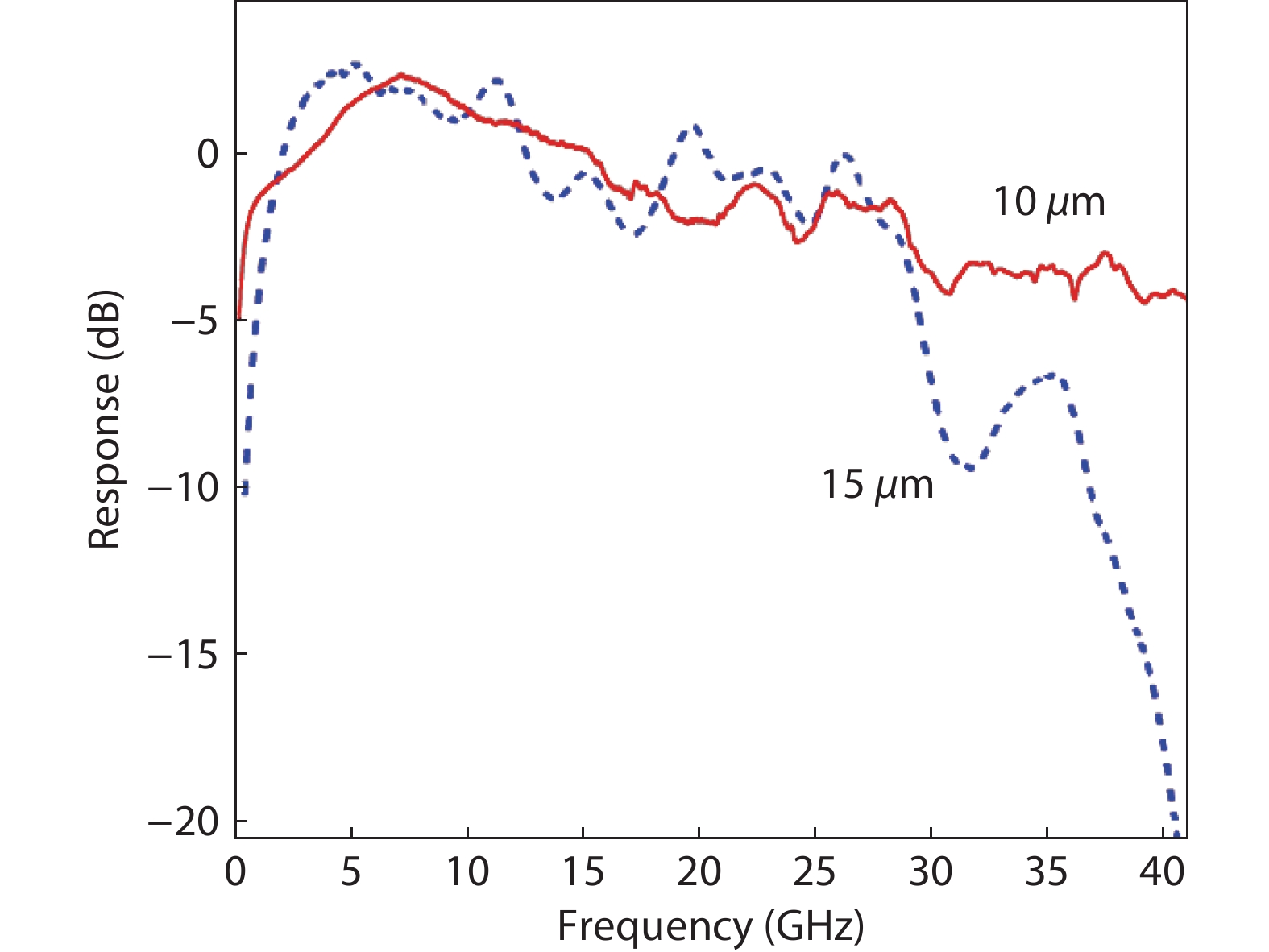
Abstract: The design, manufacturing and DC and microwave characterization of high-power Schottky barrier InAlAs/InGaAs back-illuminated mesa structure photodiodes are presented. The photodiodes with 10 and 15 μm mesa diameters operate at ≥40 and 28 GHz, respectively, have the output RF power as high as 58 mW at a frequency of 20 GHz, the DC responsivity of up to 1.08 A/W depending on the absorbing layer thickness, and a photodiode dark current as low as 0.04 nA. We show that these photodiodes provide an advantage in the amplitude-to-phase conversion factor which makes them suitable for use in high-speed analog transmission lines with stringent requirements for phase noise.

Key words: InAlAs/InGaAs heterostructuresmicrowave photodiodesmicrowave photonics


[1]
Liu P L, Williams K J, Frankel M Y, et al. Saturation characteristics of fast photodetectors. IEEE Trans Microw Theory Tech, 1999, 47, 1297 doi: 10.1109/22.775469
[2]
Li X W, Li N, Demiguel S, et al. A partially depleted absorber photodiode with graded doping injection regions. IEEE Photonics Technol Lett, 2004, 16, 2326 doi: 10.1109/LPT.2004.834563
[3]
Seeds A J, Williams K J. Microwave photonics. J Light Technol, 2006, 24, 4628 doi: 10.1109/JLT.2006.885787
[4]
Nagatsuma T, Ito H, Ishibashi T. High-power RF photodiodes and their applications. Laser Photonics Rev, 2009, 3, 123 doi: 10.1002/lpor.200810024
[5]
Rouvalis E, Baynes F N, Xie X J, et al. High-power and high-linearity photodetector modules for microwave photonic applications. J Light Technol, 2014, 32, 3810 doi: 10.1109/JLT.2014.2310252
[6]
Chizh A, Malyshev S, Mikitchuk K. High-speed high-power InAlAs/InGaAs/InP Schottky photodiode. 2015 International Topical Meeting on Microwave Photonics (MWP), 2015, 1
[7]
Chizh A L, Mikitchuk K B, Zhuravlev K S, et al. High-power high-speed Schottky photodiodes for analog fiber-optic microwave signal transmission lines. Tech Phys Lett, 2019, 45, 739 doi: 10.1134/S1063785019070204
[8]
Dmitriev D V, Kolosovsky D A, Gavrilova T A, et al. Transformation of the InP(001) surface upon annealing in an arsenic flux. Surf Sci, 2021, 710, 121861 doi: 10.1016/j.susc.2021.121861
[9]
Dmitriev D V, Valisheva N A, Gilinsky A M, et al. InAlAs/InGaAs/InP heterostructures for microwave photodiodes grown by molecular beam epitaxy. IOP Conf Ser: Mater Sci Eng, 2019, 475, 012022 doi: 10.1088/1757-899X/475/1/012022
[10]
Aksenov M S, Valisheva N A, Chistokhin I B, et al. About the nature of the barrier inhomogeneities at Au/Ti/n-InAlAs(001) Schottky contacts. Appl Phys Lett, 2019, 114, 221602 doi: 10.1063/1.5091598
[11]
Born M, Wolf E. Principles of optics. 7th ed. Cambridge University Press, 1999, 64
[12]
Rogalski A. Infrared detectors. 2nd ed. CRC Press, 2010, 182
[13]
Zielinski E, Schweizer H, Streubel K, et al. Excitonic transitions and exciton damping processes in InGaAs/InP. J Appl Phys, 1986, 59, 2196 doi: 10.1063/1.336358
[14]
Kato K, Hata S, Kawano K, et al. Design of ultrawide-band, high-sensitivity p–i–n photodetectors. IEICE Trans Electron, 1993, E76-C, 214
[15]
Chtioui M, Enard A, Carpentier D, et al. High-power high-linearity uni-traveling-carrier photodiodes for analog photonic links. IEEE Photonics Technol Lett, 2008, 20, 202 doi: 10.1109/LPT.2007.913260
[16]
Rubiola E, Salik E, Yu N, et al. Flicker noise in high-speed p-i-n photodiodes. IEEE Trans Microw Theory Tech, 2006, 54, 816 doi: 10.1109/TMTT.2005.863062
[17]
Eliyahu D, Seidel D, Maleki L. RF amplitude and phase-noise reduction of an optical link and an opto-electronic oscillator. IEEE Trans Microw Theory Tech, 2008, 56, 449 doi: 10.1109/TMTT.2007.914640
[18]
Hu Y, Menyuk C R, Xie X J, et al. Computational study of amplitude-to-phase conversion in a modified unitraveling carrier photodetector. IEEE Photonics J, 2017, 9, 1 doi: 10.1109/JPHOT.2017.2682251
[19]
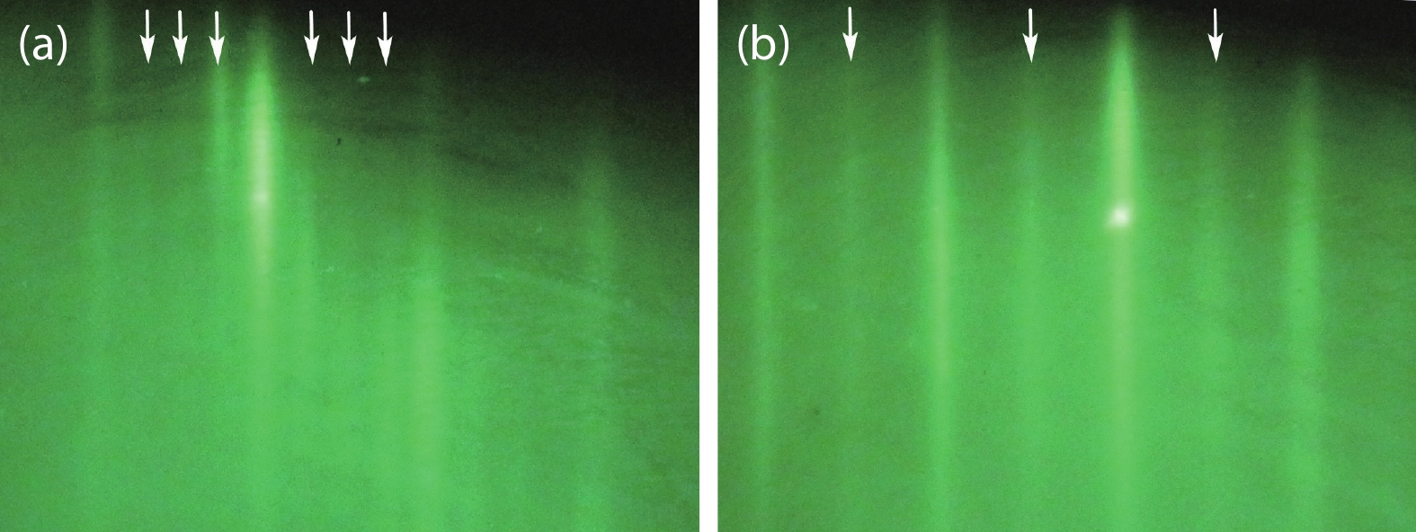
Fig. 1.  (Color online) The (4 × 2) reconstruction of the clean surface of (001) InP after annealing seen in the RHEED images: (a) the $\left[ {1\,\bar 1\,0} \right] $ azimuth, (b) the [$1\,1\,0 $] azimuth. The arrows indicate reflexes corresponding to the period by (a) 4 times and (b) 2 times greater than the crystal lattice period.

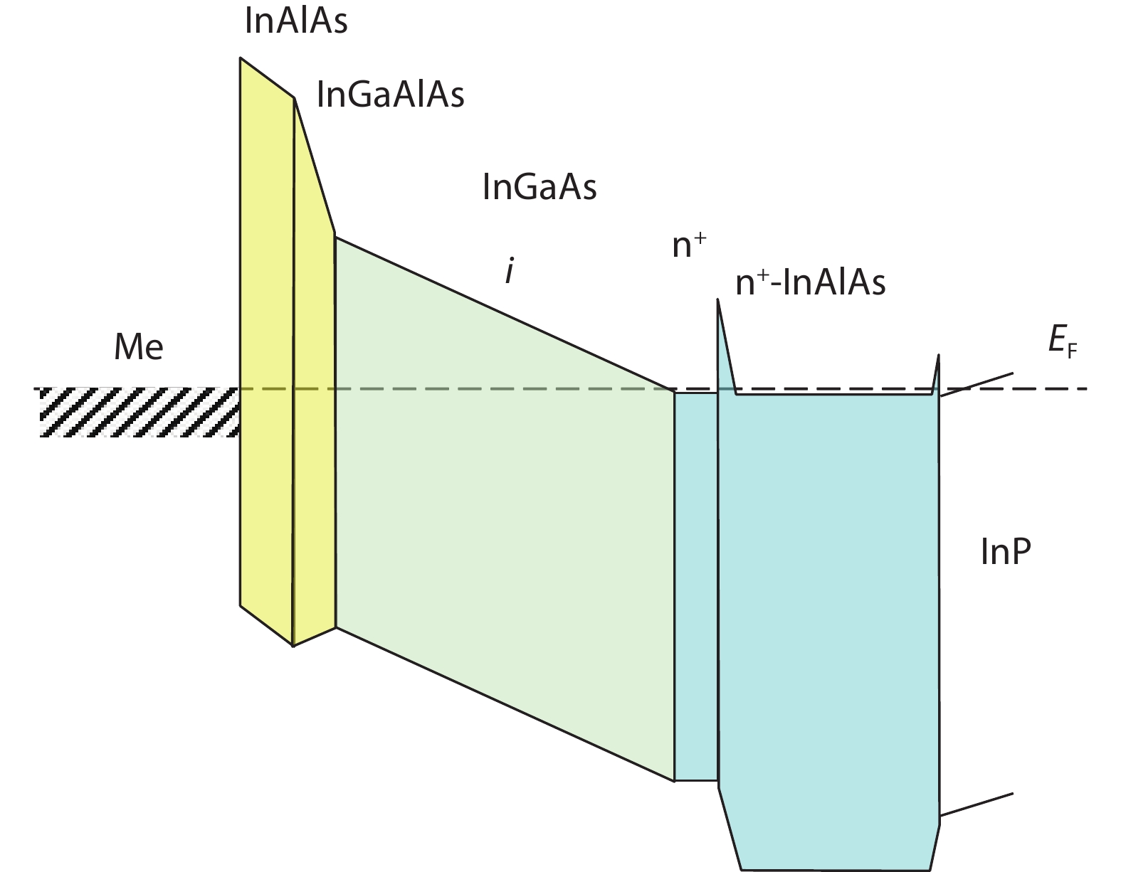
Fig. 2.  (Color online) Energy band diagram of the InAlAs/InGaAs Schottky barrier photodiode under zero bias voltage. EF is the Fermi level and Me is the Schottky barrier metal.

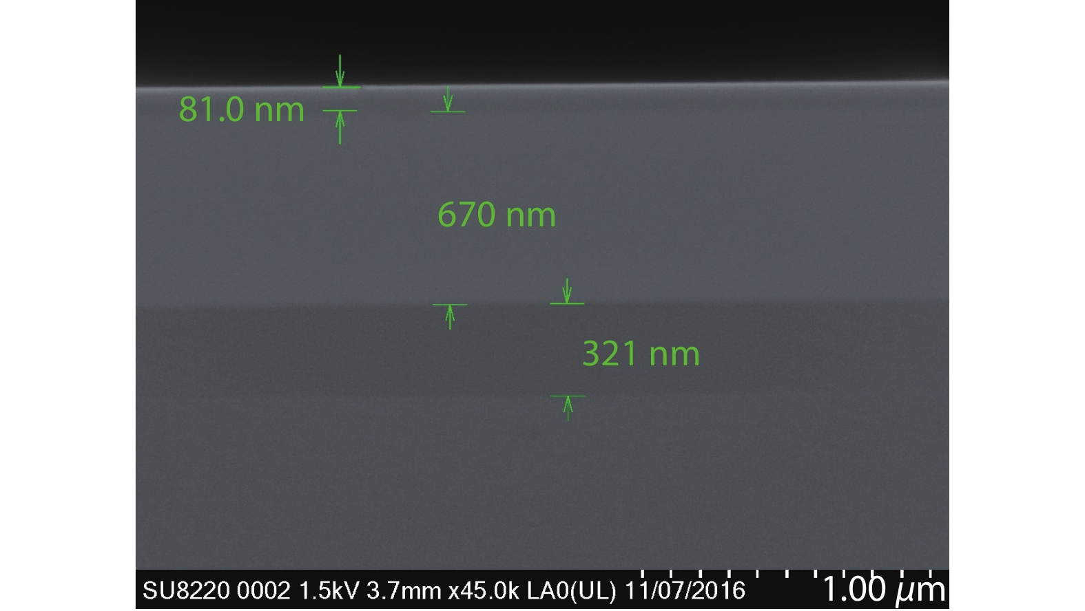
Fig. 3.  (Color online) A SEM picture of a heterostructure sample with a total intended thickness of the absorbing layer of 650 nm. Layers of InGaAs appear brighter in intensity than InAlAs-based layers. The visible sets of different contrast layers are, from top to bottom: the InAlAs barrier and InGaAlAs graded bandgap layers together with the InGaAs protective layer; the InGaAs absorbing layer; the n+-InAlAs contact layer; the InP substrate. The green marks denote the layer thicknesses as seen by the SEM.

Fig. 4.  (Color online) Optical reflection spectrum of a model heterostructure used to evaluate the Schottky contact reflection efficiency. The spectral resolution is set to average the interference fringes that develop in the spectral region < Eg. The diagrams illustrate the mechanisms of reflection for photon energies above the bandgap Eg of the InGaAs absorbing layer (left) and for < Eg (right). The inset at the top shows the photograph of a photodiode chip.

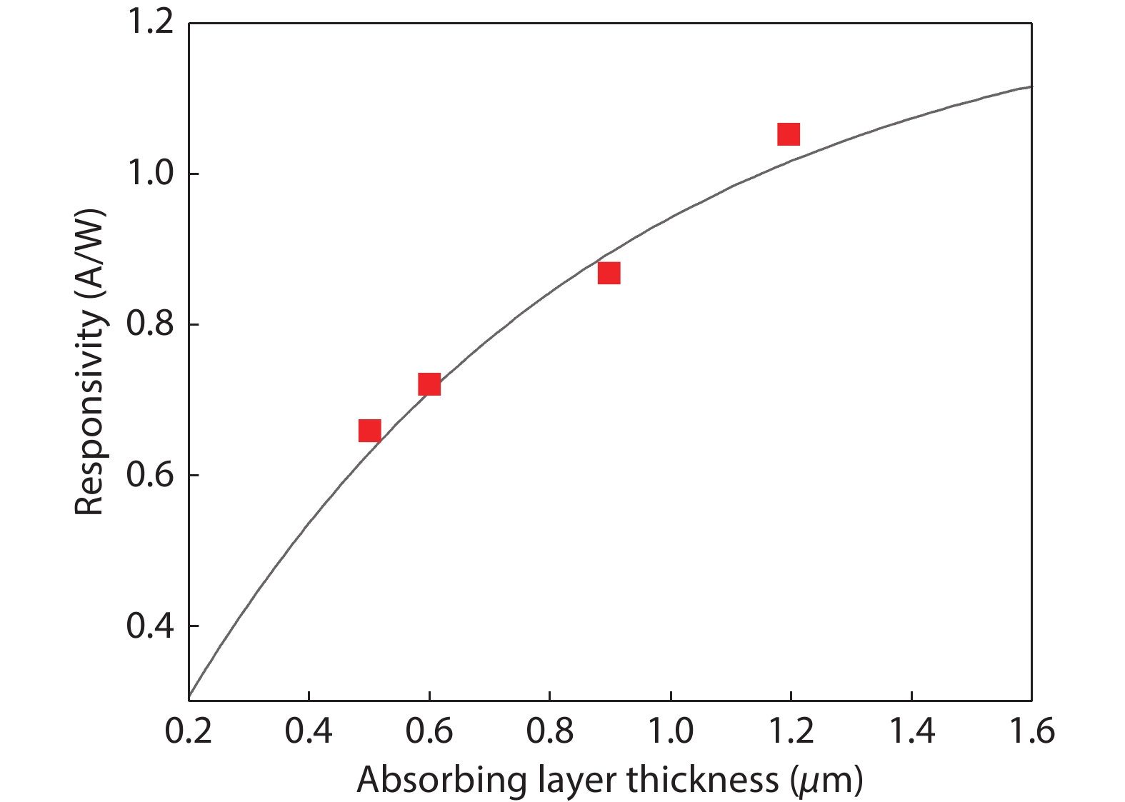
Fig. 5.  (Color online) The dependence of the photodiode responsivity on the absorbing layer thickness at a wavelength of 1.55 μm. Squares display the experimental data and the solid line is a model calculation.

Fig. 6.  (Color online) The frequency response of a 10 μm (solid line) and 15 μm (dashed line) diameter photodiodes.

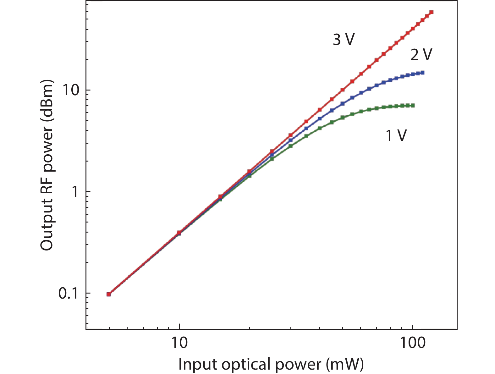
Fig. 7.  (Color online) RF output power of a 15 μm diameter photodiode as a function of the input optical power for bias voltages of 1, 2 and 3 V. Modulation frequency 20 GHz.

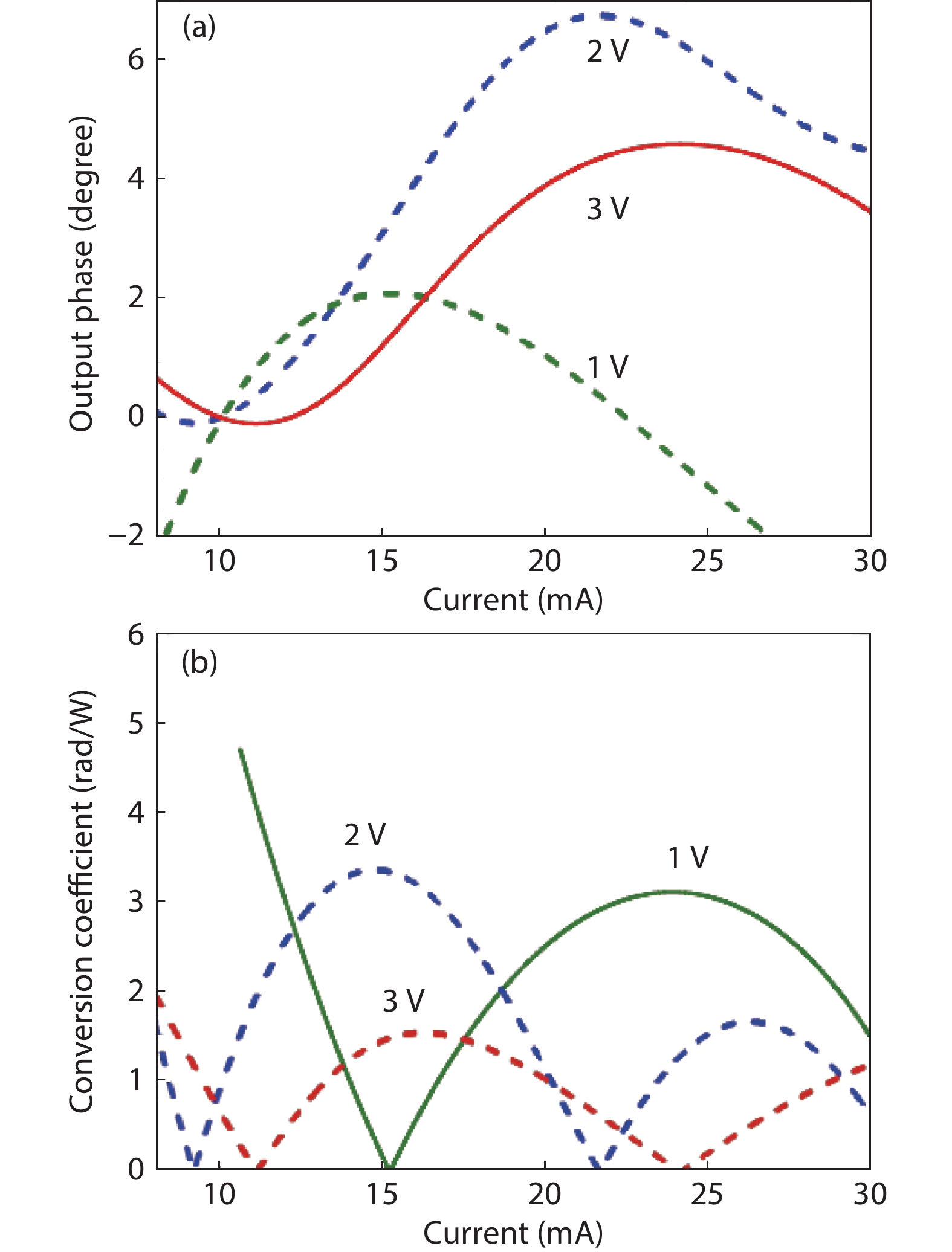
Fig. 8.  (Color online) (a) Dependence of the phase of the output RF signal of a 15 μm diameter photodiode on the photodiode photocurrent for bias voltages of 1, 2 and 3 V. (b) Amplitude-to- phase conversion coefficient dependencies calculated from the data of (a).

Table 1.   InAlAs/InGaAs heteroepitaxial structure of the Schottky barrier high-power microwave photodiode.

Layer compositionLayer thicknessLayer description
In0.53Ga0.47As30 nmProtective layer
In0.52Al0.48As30 nm Barrier layer
InGaAlAs50 nm Graded bandgap layer
In0.53Ga0.47As500–1200 nmUndoped absorbing layer
In0.53Ga0.47As:Si50 nmAbsorbing n+-layer (5 × 1018 cm−3)
In0.52Al0.48As:Si300 nmContact n+-layer (5 × 1018 cm−3)
InP(001) > 350 μm Substrate
DownLoad: CSV
[1]
Liu P L, Williams K J, Frankel M Y, et al. Saturation characteristics of fast photodetectors. IEEE Trans Microw Theory Tech, 1999, 47, 1297 doi: 10.1109/22.775469
[2]
Li X W, Li N, Demiguel S, et al. A partially depleted absorber photodiode with graded doping injection regions. IEEE Photonics Technol Lett, 2004, 16, 2326 doi: 10.1109/LPT.2004.834563
[3]
Seeds A J, Williams K J. Microwave photonics. J Light Technol, 2006, 24, 4628 doi: 10.1109/JLT.2006.885787
[4]
Nagatsuma T, Ito H, Ishibashi T. High-power RF photodiodes and their applications. Laser Photonics Rev, 2009, 3, 123 doi: 10.1002/lpor.200810024
[5]
Rouvalis E, Baynes F N, Xie X J, et al. High-power and high-linearity photodetector modules for microwave photonic applications. J Light Technol, 2014, 32, 3810 doi: 10.1109/JLT.2014.2310252
[6]
Chizh A, Malyshev S, Mikitchuk K. High-speed high-power InAlAs/InGaAs/InP Schottky photodiode. 2015 International Topical Meeting on Microwave Photonics (MWP), 2015, 1
[7]
Chizh A L, Mikitchuk K B, Zhuravlev K S, et al. High-power high-speed Schottky photodiodes for analog fiber-optic microwave signal transmission lines. Tech Phys Lett, 2019, 45, 739 doi: 10.1134/S1063785019070204
[8]
Dmitriev D V, Kolosovsky D A, Gavrilova T A, et al. Transformation of the InP(001) surface upon annealing in an arsenic flux. Surf Sci, 2021, 710, 121861 doi: 10.1016/j.susc.2021.121861
[9]
Dmitriev D V, Valisheva N A, Gilinsky A M, et al. InAlAs/InGaAs/InP heterostructures for microwave photodiodes grown by molecular beam epitaxy. IOP Conf Ser: Mater Sci Eng, 2019, 475, 012022 doi: 10.1088/1757-899X/475/1/012022
[10]
Aksenov M S, Valisheva N A, Chistokhin I B, et al. About the nature of the barrier inhomogeneities at Au/Ti/n-InAlAs(001) Schottky contacts. Appl Phys Lett, 2019, 114, 221602 doi: 10.1063/1.5091598
[11]
Born M, Wolf E. Principles of optics. 7th ed. Cambridge University Press, 1999, 64
[12]
Rogalski A. Infrared detectors. 2nd ed. CRC Press, 2010, 182
[13]
Zielinski E, Schweizer H, Streubel K, et al. Excitonic transitions and exciton damping processes in InGaAs/InP. J Appl Phys, 1986, 59, 2196 doi: 10.1063/1.336358
[14]
Kato K, Hata S, Kawano K, et al. Design of ultrawide-band, high-sensitivity p–i–n photodetectors. IEICE Trans Electron, 1993, E76-C, 214
[15]
Chtioui M, Enard A, Carpentier D, et al. High-power high-linearity uni-traveling-carrier photodiodes for analog photonic links. IEEE Photonics Technol Lett, 2008, 20, 202 doi: 10.1109/LPT.2007.913260
[16]
Rubiola E, Salik E, Yu N, et al. Flicker noise in high-speed p-i-n photodiodes. IEEE Trans Microw Theory Tech, 2006, 54, 816 doi: 10.1109/TMTT.2005.863062
[17]
Eliyahu D, Seidel D, Maleki L. RF amplitude and phase-noise reduction of an optical link and an opto-electronic oscillator. IEEE Trans Microw Theory Tech, 2008, 56, 449 doi: 10.1109/TMTT.2007.914640
[18]
Hu Y, Menyuk C R, Xie X J, et al. Computational study of amplitude-to-phase conversion in a modified unitraveling carrier photodetector. IEEE Photonics J, 2017, 9, 1 doi: 10.1109/JPHOT.2017.2682251
[19]
  • Search

    Advanced Search >>

    GET CITATION

    shu

    Export: BibTex EndNote

    Article Metrics

    Article views: 1928 Times PDF downloads: 72 Times Cited by: 0 Times

    History

    Received: 19 May 2021 Revised: 05 July 2021 Online: Accepted Manuscript: 07 September 2021Uncorrected proof: 08 September 2021Published: 04 January 2022

    Catalog

      Email This Article

      User name:
      Email:*请输入正确邮箱
      Code:*验证码错误
      K. S. Zhuravlev, A. L. Chizh, K. B. Mikitchuk, A. M. Gilinsky, I. B. Chistokhin, N. A. Valisheva, D. V. Dmitriev, A. I. Toropov, M. S. Aksenov. High-power InAlAs/InGaAs Schottky barrier photodiodes for analog microwave signal transmission[J]. Journal of Semiconductors, 2022, 43(1): 012302. doi: 10.1088/1674-4926/43/1/012302 K S Zhuravlev, A L Chizh, K B Mikitchuk, A M Gilinsky, I B Chistokhin, N A Valisheva, D V Dmitriev, A I Toropov, M S Aksenov, High-power InAlAs/InGaAs Schottky barrier photodiodes for analog microwave signal transmission[J]. J. Semicond., 2022, 43(1): 012302. doi: 10.1088/1674-4926/43/1/012302.Export: BibTex EndNote
      Citation:
      K. S. Zhuravlev, A. L. Chizh, K. B. Mikitchuk, A. M. Gilinsky, I. B. Chistokhin, N. A. Valisheva, D. V. Dmitriev, A. I. Toropov, M. S. Aksenov. High-power InAlAs/InGaAs Schottky barrier photodiodes for analog microwave signal transmission[J]. Journal of Semiconductors, 2022, 43(1): 012302. doi: 10.1088/1674-4926/43/1/012302

      K S Zhuravlev, A L Chizh, K B Mikitchuk, A M Gilinsky, I B Chistokhin, N A Valisheva, D V Dmitriev, A I Toropov, M S Aksenov, High-power InAlAs/InGaAs Schottky barrier photodiodes for analog microwave signal transmission[J]. J. Semicond., 2022, 43(1): 012302. doi: 10.1088/1674-4926/43/1/012302.
      Export: BibTex EndNote

      High-power InAlAs/InGaAs Schottky barrier photodiodes for analog microwave signal transmission

      doi: 10.1088/1674-4926/43/1/012302
      More Information
      • Author Bio:

        K. S. Zhuravlev currently heads a laboratory at Rzhanov Institute of Semiconductor Physics, the Siberian Brach of the Russian Academy of Sciences (ISP SB RAS). His research interests were aimed at radiative recombination in various GaAs-based and low-dimensional structures, Si and II–VI nanocrystals, and device-related physics and technology, including nitride material system. At present his research is focused on the MBE growth and studies of III-V structures, design and fabrication of new type of heterostructures for optical and electronic high frequency devices

      • Corresponding author: zhur@isp.nsc.ru
      • Received Date: 2021-05-19
      • Revised Date: 2021-07-05
      • Published Date: 2022-01-10

      Catalog

        /

        DownLoad:  Full-Size Img  PowerPoint
        Return
        Return