


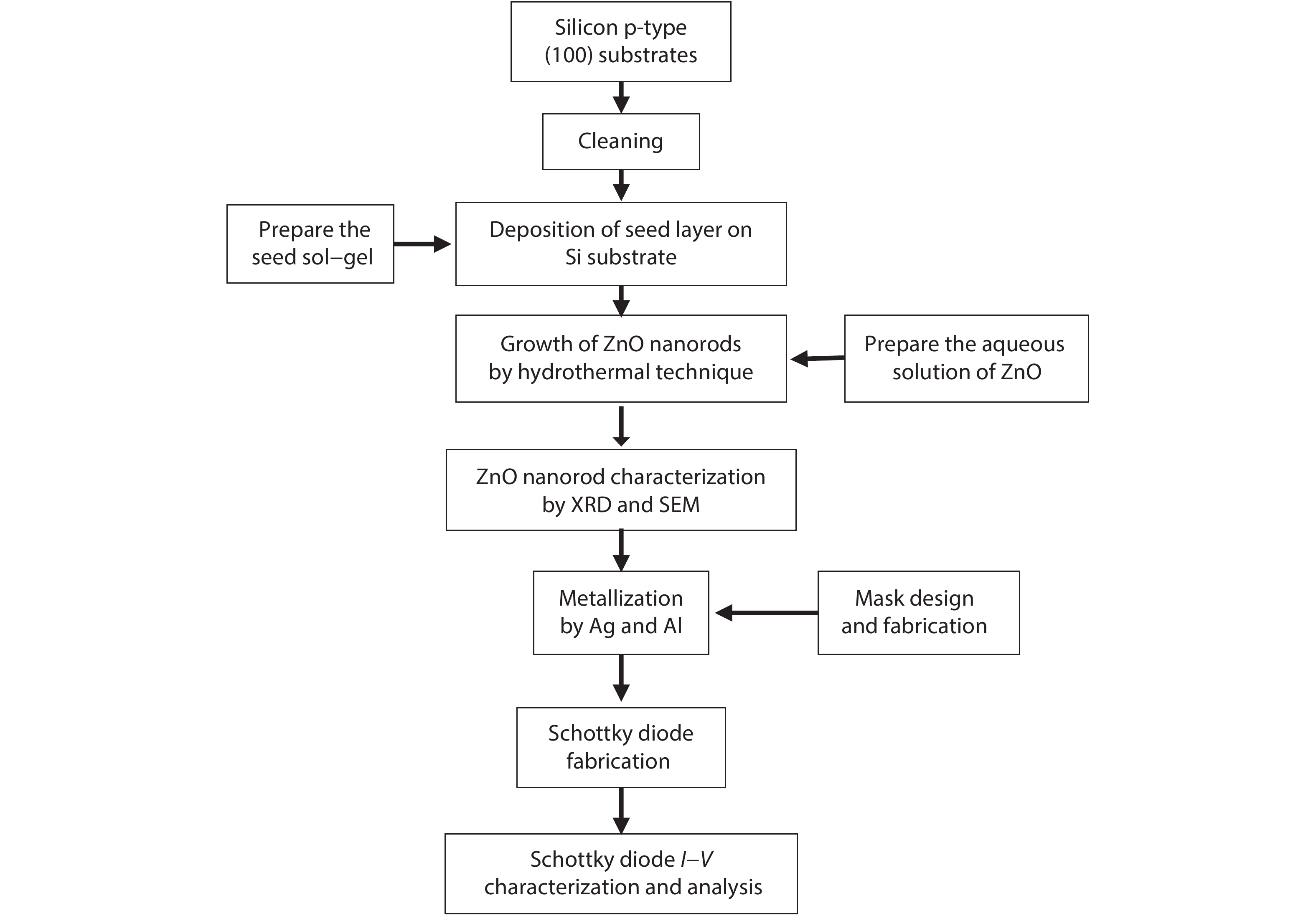
Fig. 1.
The block diagram of the experimental work.
ARTICLES
Ghusoon M. Ali, Ahmed K. Khalid and Salah M. Swadi
Corresponding author: Ghusoon M. Ali, Email: ghusoon.ali@gmail.com
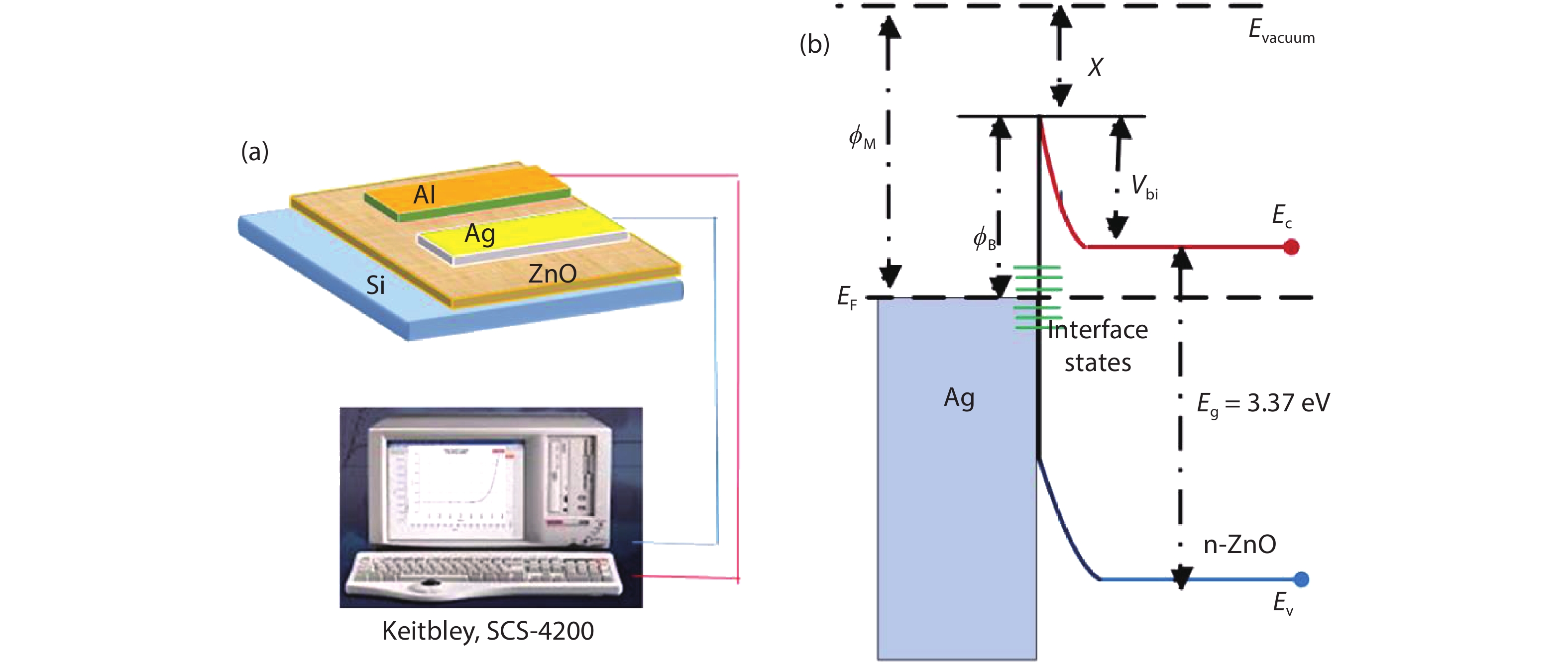
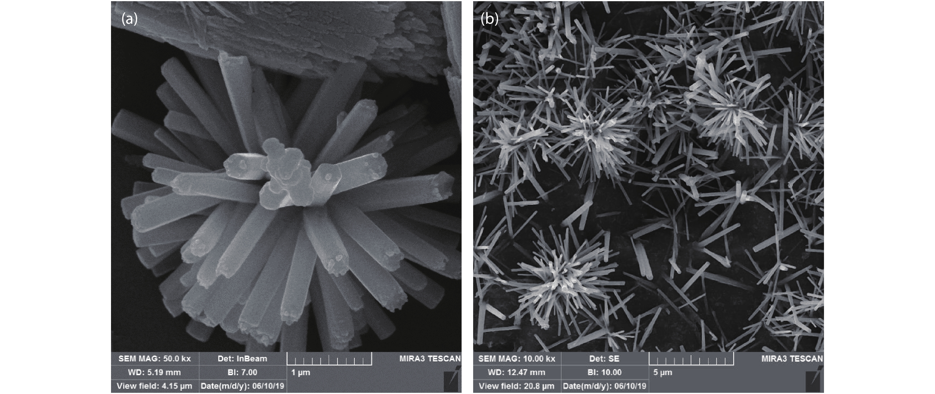
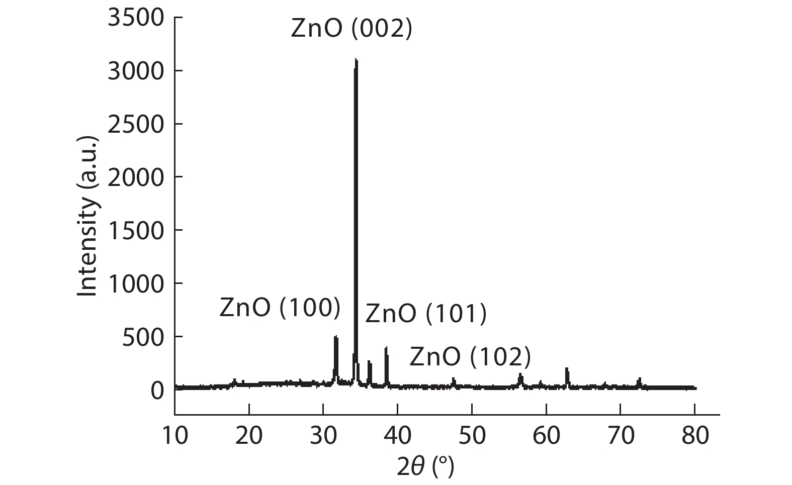
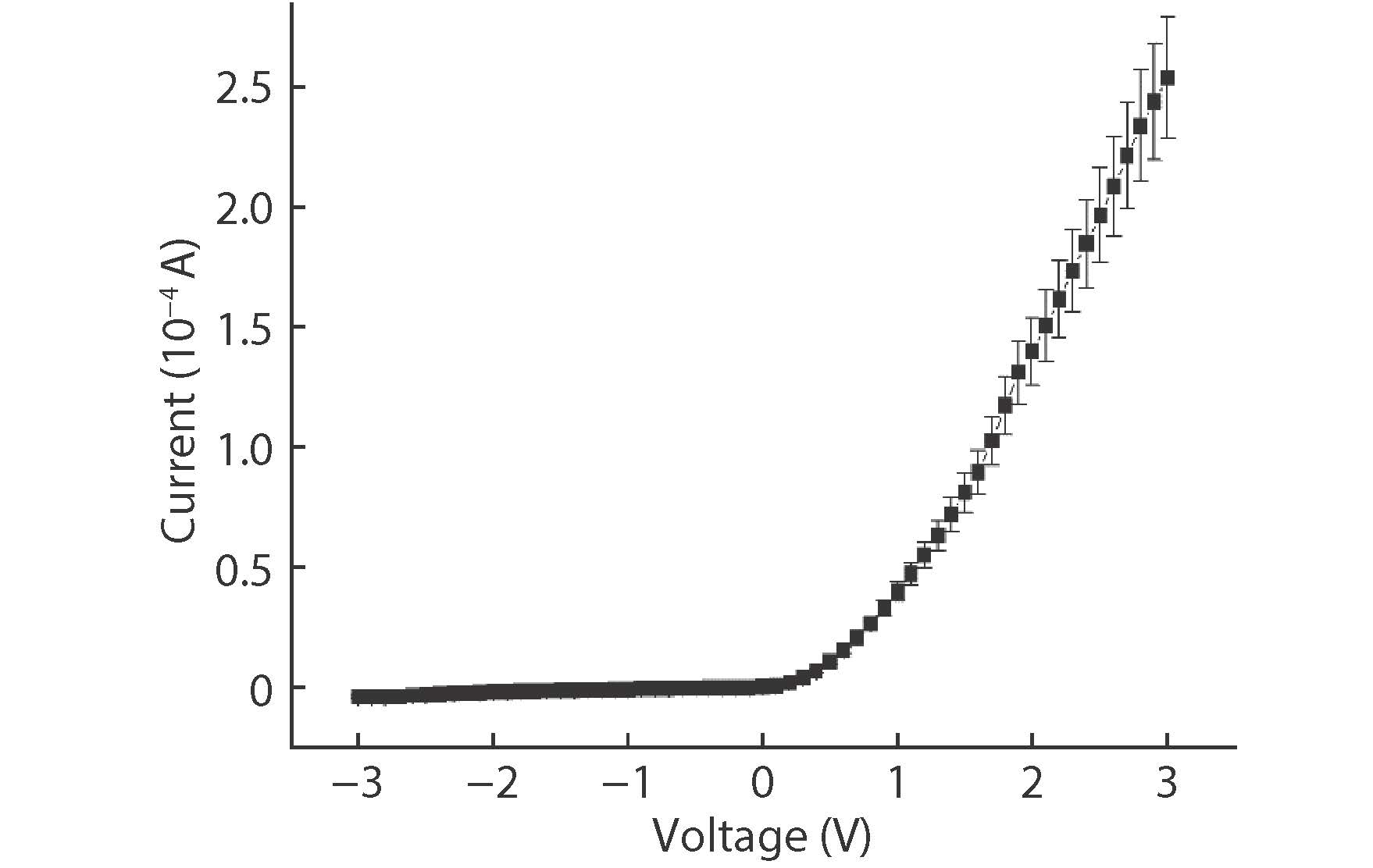
Abstract: This paper reports the realization of planar Schottky diodes based on nanorod ZnO thin film. The nanorod ZnO thin film was fabricated by hydrothermal technique on boron doped p-type Si (100) substrate. The Ag//ZnO/Al planar diode operating with voltage bias from –3 to 3 V. The I–V characteristics clearly indicate that the devices have rectifying performance. The thermionic emission theory governs the current across the studied Schottky diode. The device achieved a turn-on voltage of 0.9 V, barrier height 0.69 eV and saturation current of 1.2 × 10⁻⁶ A. The diode shows a very large ideality factor (n > > 2) which is attributed to high interface trap concentration. The surface topology was investigated by scanning electron microscope (SEM). The structural properties of the nanostructured ZnO thin film were characterized by X-ray diffraction (XRD). The SEM images reveal that the ZnO nanorods grow perpendicular to the substrate with uniformity and high density. The XRD pattern illustrates the dominant peak appearing at (002). This intense peak indicates the c-axis orientated phase of the wurtzite ZnO structure. It demonstrates that the crystals grow uniformly perpendicular to the substrate surface in good agreement with the SEM images.
| [1] |
Tsao J Y. Ultrawide-bandgap semiconductors: research opportunities and challenges. Adv Electron Mater, 2018, 4, 1 doi: 10.1002/aelm.201600501
|
| [2] |
Sze S M. Physics of semiconductor devices. New York: John Wiley & Sons, Inc., 2006
|
| [3] |
Brillson L J, Lu Y. ZnO Schottky barriers and Ohmic contacts. J Appl Phys, 2011, 109, 8 doi: 10.1063/1.3581173
|
| [4] |
Borysiewicz M A, Kamińska E, Myşliwiec M, et al. Fundamentals and practice of metal contacts to wide band gap semiconductor devices. Cryst Res Technol, 2012, 47, 261 doi: 10.1002/crat.201100490
|
| [5] |
Ali G M. Interdigitated extended gate field effect transistor without reference electrode. J Electron Mater, 2017, 46(2), 713 doi: 10.1007/s11664-016-5041-0
|
| [6] |
Yadav A B, Pandey A, Jit S. Pd Schottky contacts on sol –gel derived ZnO. IEEE Electron Device Lett, 2014, 35, 729 doi: 10.1109/LED.2014.2319578
|
| [7] |
Somvanshi D, Jit S. Analysis of temperature-dependent electrical characteristics of n-ZnO Nanowires (NWs)/p-Si heterojunction diodes. IEEE Trans Nanotechnol, 2014, 13, 62 doi: 10.1109/TNANO.2013.2290553
|
| [8] |
Roy S, Das S, Sarkar C K. Investigation of nanostructured Pd–Ag/n-ZnO thin film based Schottky junction for methane sensing. Int Nano Lett, 2016, 6, 199 doi: 10.1007/s40089-016-0187-6
|
| [9] |
Ali G M, Dhaher R H, Abdullateef A A. PH sensing characteristics of EGFET based on Pd-doped ZnO thin films synthesized by sol-gel method. 3rd International Conference on Technological Advances in Electrical, Electronics and Computer Engineering, 2015
|
| [10] |
Mead C A. Surface barriers on ZnSe and ZnO. Phys Lett, 1965, 18, 218 doi: 10.1016/0031-9163(65)90295-7
|
| [11] |
Neville R C, Mead C A. Surface barriers on zinc oxide. J Appl Phys, 1970, 41, 3795 doi: 10.1063/1.1659509
|
| [12] |
Somvanshi D, Jit S. Effects of Sn and Zn seed layers on the electrical characteristics of Pd/ZnO thin-film Schottky diodes grown on n-Si substrates. IEEE Electron Device Lett, 2014, 35, 945 doi: 10.1109/LED.2014.2334473
|
| [13] |
Ali G M, Chakrabarti P. Fabrication and characterization of thin film ZnO Schottky contacts based UV photodetectors: A comparative study. J Vac Sci Technol B, 2012, 30, 031206 doi: 10.1116/1.3701945
|
| [14] |
Singh S, Chakrabarti P. Comparison of the structural and optical properties of ZnO thin films deposited by three different methods for optoelectronic applications. Superlattices Microstruct, 2013, 64, 283 doi: 10.1016/j.spmi.2013.09.031
|
| [15] |
Somvanshi D, Jit S. Effect of ZnO seed layer on the electrical characteristics of Pd/ZnO thin-film-based schottky contacts grown on n-Si substrates. IEEE Trans Nanotechnol, 2014, 13, 1138 doi: 10.1109/TNANO.2014.2343965
|
| [16] |
Sharma S, Vyas S, Periasamy C, et al. Structural and optical characterization of ZnO thin films for optoelectronic device applications by RF sputtering technique. Superlattices Microstruct, 2014, 75, 378 doi: 10.1016/j.spmi.2014.07.032
|
| [17] |
Baruah S, Dutta J. Hydrothermal growth of ZnO nanostructures. Sci Technol Adv Mater, 2009, 10(1), 013001 doi: 10.1088/1468-6996/10/1/013001
|
| [18] |
Zhang H, Chen W, Li Y, et al. 3D flower-like NiO hierarchical structures assembled with size-controllable 1D blocking units: Gas sensing performances towards. Acetylene, 2018, 6, 1 doi: 10.3389/fchem.2018.00472
|
| [19] |
Gokarna A, Pavaskar N R, Sathaye S D, et al. Electroluminescence from heterojunctions of nanocrystalline CdS and ZnS with porous silicon. J Appl Phys, 2002, 92, 2118 doi: 10.1063/1.1483381
|
| [20] |
Ali G M, Dwivedi A D D, Singh S, et al. Interface properties and junction behavior of Pd contact on ZnO thin film grown by vacuum deposition technique. Phys Status Solidi C, 2010, 7(2), 252 doi: 10.1002/pssc.200982409
|


Article views: 4833 Times PDF downloads: 76 Times Cited by: 0 Times
Received: 02 January 2020 Revised: 14 February 2020 Online: Accepted Manuscript: 09 April 2020Uncorrected proof: 17 April 2020Published: 01 October 2020
| Citation: |
Ghusoon M. Ali, Ahmed K. Khalid, Salah M. Swadi. Nanoflower ZnO thin-film grown by hydrothermal technique based Schottky diode[J]. Journal of Semiconductors, 2020, 41(10): 102103. doi: 10.1088/1674-4926/41/10/102103
****
G M Ali, A K Khalid, S M Swadi, Nanoflower ZnO thin-film grown by hydrothermal technique based Schottky diode[J]. J. Semicond., 2020, 41(10): 102103. doi: 10.1088/1674-4926/41/10/102103.

|
| [1] |
Tsao J Y. Ultrawide-bandgap semiconductors: research opportunities and challenges. Adv Electron Mater, 2018, 4, 1 doi: 10.1002/aelm.201600501
|
| [2] |
Sze S M. Physics of semiconductor devices. New York: John Wiley & Sons, Inc., 2006
|
| [3] |
Brillson L J, Lu Y. ZnO Schottky barriers and Ohmic contacts. J Appl Phys, 2011, 109, 8 doi: 10.1063/1.3581173
|
| [4] |
Borysiewicz M A, Kamińska E, Myşliwiec M, et al. Fundamentals and practice of metal contacts to wide band gap semiconductor devices. Cryst Res Technol, 2012, 47, 261 doi: 10.1002/crat.201100490
|
| [5] |
Ali G M. Interdigitated extended gate field effect transistor without reference electrode. J Electron Mater, 2017, 46(2), 713 doi: 10.1007/s11664-016-5041-0
|
| [6] |
Yadav A B, Pandey A, Jit S. Pd Schottky contacts on sol –gel derived ZnO. IEEE Electron Device Lett, 2014, 35, 729 doi: 10.1109/LED.2014.2319578
|
| [7] |
Somvanshi D, Jit S. Analysis of temperature-dependent electrical characteristics of n-ZnO Nanowires (NWs)/p-Si heterojunction diodes. IEEE Trans Nanotechnol, 2014, 13, 62 doi: 10.1109/TNANO.2013.2290553
|
| [8] |
Roy S, Das S, Sarkar C K. Investigation of nanostructured Pd–Ag/n-ZnO thin film based Schottky junction for methane sensing. Int Nano Lett, 2016, 6, 199 doi: 10.1007/s40089-016-0187-6
|
| [9] |
Ali G M, Dhaher R H, Abdullateef A A. PH sensing characteristics of EGFET based on Pd-doped ZnO thin films synthesized by sol-gel method. 3rd International Conference on Technological Advances in Electrical, Electronics and Computer Engineering, 2015
|
| [10] |
Mead C A. Surface barriers on ZnSe and ZnO. Phys Lett, 1965, 18, 218 doi: 10.1016/0031-9163(65)90295-7
|
| [11] |
Neville R C, Mead C A. Surface barriers on zinc oxide. J Appl Phys, 1970, 41, 3795 doi: 10.1063/1.1659509
|
| [12] |
Somvanshi D, Jit S. Effects of Sn and Zn seed layers on the electrical characteristics of Pd/ZnO thin-film Schottky diodes grown on n-Si substrates. IEEE Electron Device Lett, 2014, 35, 945 doi: 10.1109/LED.2014.2334473
|
| [13] |
Ali G M, Chakrabarti P. Fabrication and characterization of thin film ZnO Schottky contacts based UV photodetectors: A comparative study. J Vac Sci Technol B, 2012, 30, 031206 doi: 10.1116/1.3701945
|
| [14] |
Singh S, Chakrabarti P. Comparison of the structural and optical properties of ZnO thin films deposited by three different methods for optoelectronic applications. Superlattices Microstruct, 2013, 64, 283 doi: 10.1016/j.spmi.2013.09.031
|
| [15] |
Somvanshi D, Jit S. Effect of ZnO seed layer on the electrical characteristics of Pd/ZnO thin-film-based schottky contacts grown on n-Si substrates. IEEE Trans Nanotechnol, 2014, 13, 1138 doi: 10.1109/TNANO.2014.2343965
|
| [16] |
Sharma S, Vyas S, Periasamy C, et al. Structural and optical characterization of ZnO thin films for optoelectronic device applications by RF sputtering technique. Superlattices Microstruct, 2014, 75, 378 doi: 10.1016/j.spmi.2014.07.032
|
| [17] |
Baruah S, Dutta J. Hydrothermal growth of ZnO nanostructures. Sci Technol Adv Mater, 2009, 10(1), 013001 doi: 10.1088/1468-6996/10/1/013001
|
| [18] |
Zhang H, Chen W, Li Y, et al. 3D flower-like NiO hierarchical structures assembled with size-controllable 1D blocking units: Gas sensing performances towards. Acetylene, 2018, 6, 1 doi: 10.3389/fchem.2018.00472
|
| [19] |
Gokarna A, Pavaskar N R, Sathaye S D, et al. Electroluminescence from heterojunctions of nanocrystalline CdS and ZnS with porous silicon. J Appl Phys, 2002, 92, 2118 doi: 10.1063/1.1483381
|
| [20] |
Ali G M, Dwivedi A D D, Singh S, et al. Interface properties and junction behavior of Pd contact on ZnO thin film grown by vacuum deposition technique. Phys Status Solidi C, 2010, 7(2), 252 doi: 10.1002/pssc.200982409
|

 WeChat ID
Journal of Semiconductors © 2017 All Rights Reserved 京ICP备05085259号-2

 DownLoad:

