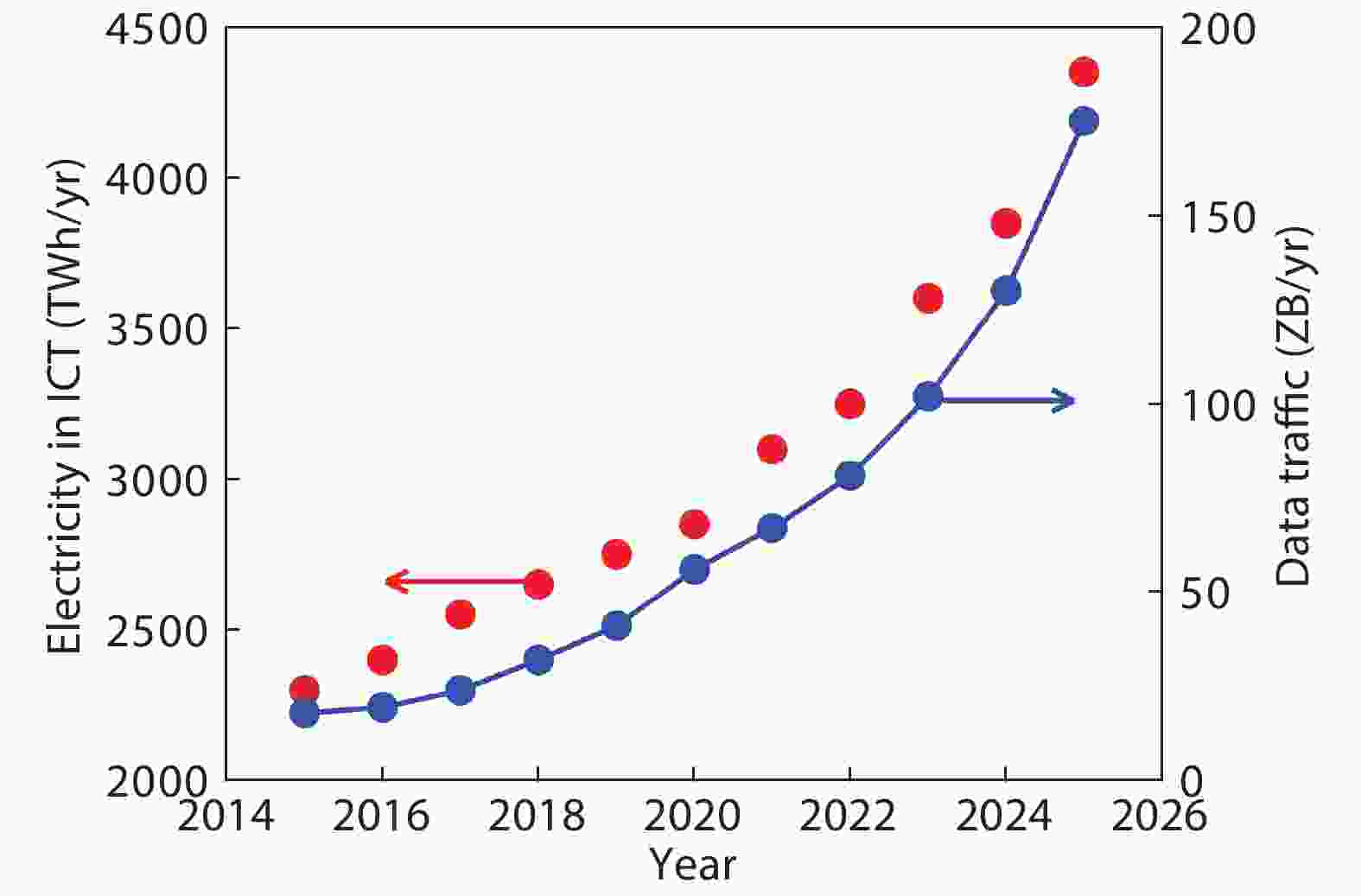
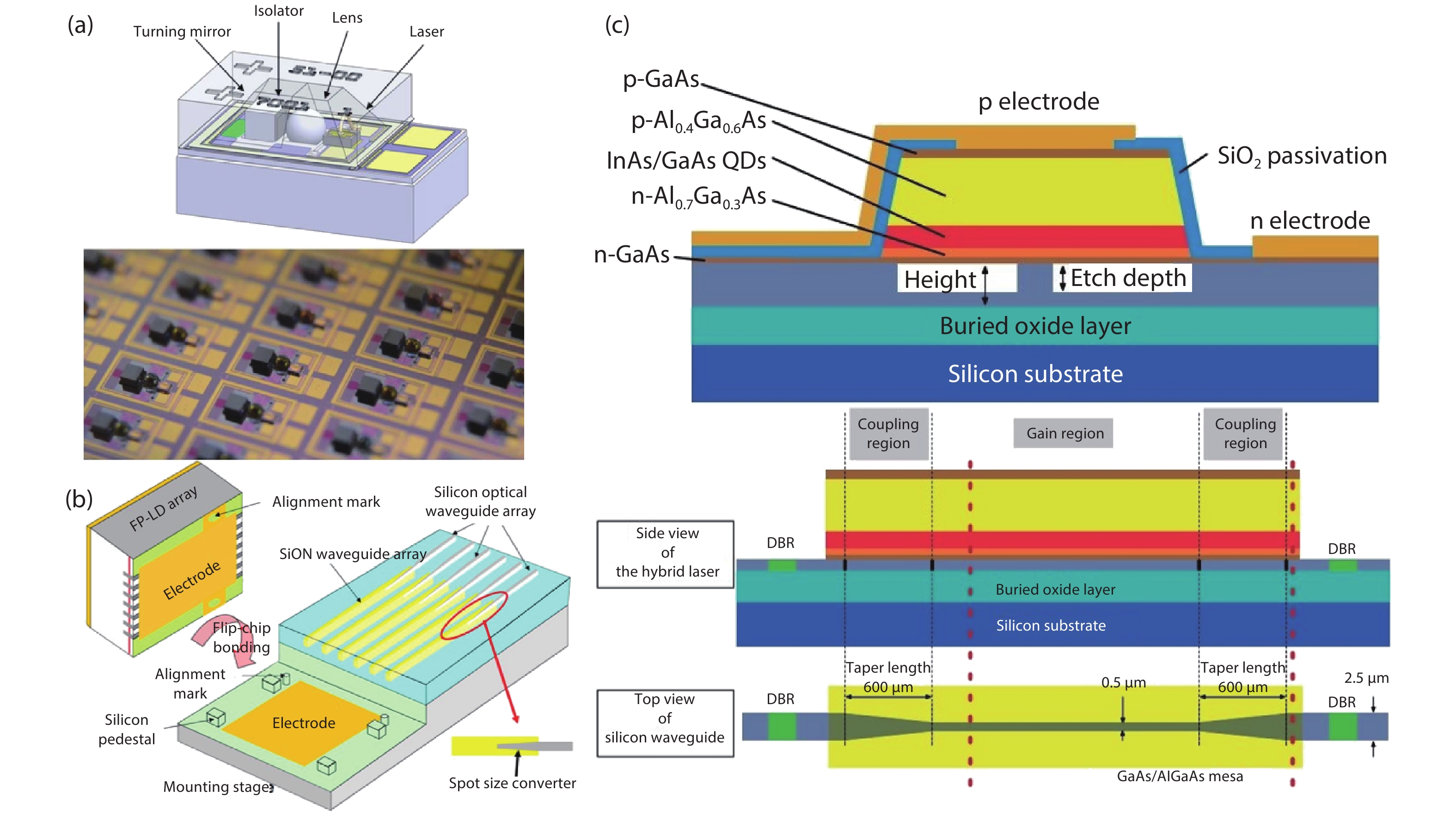
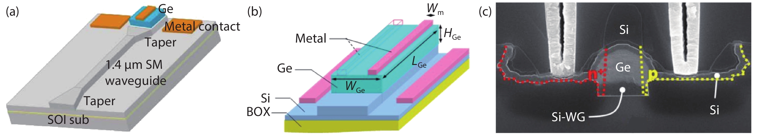
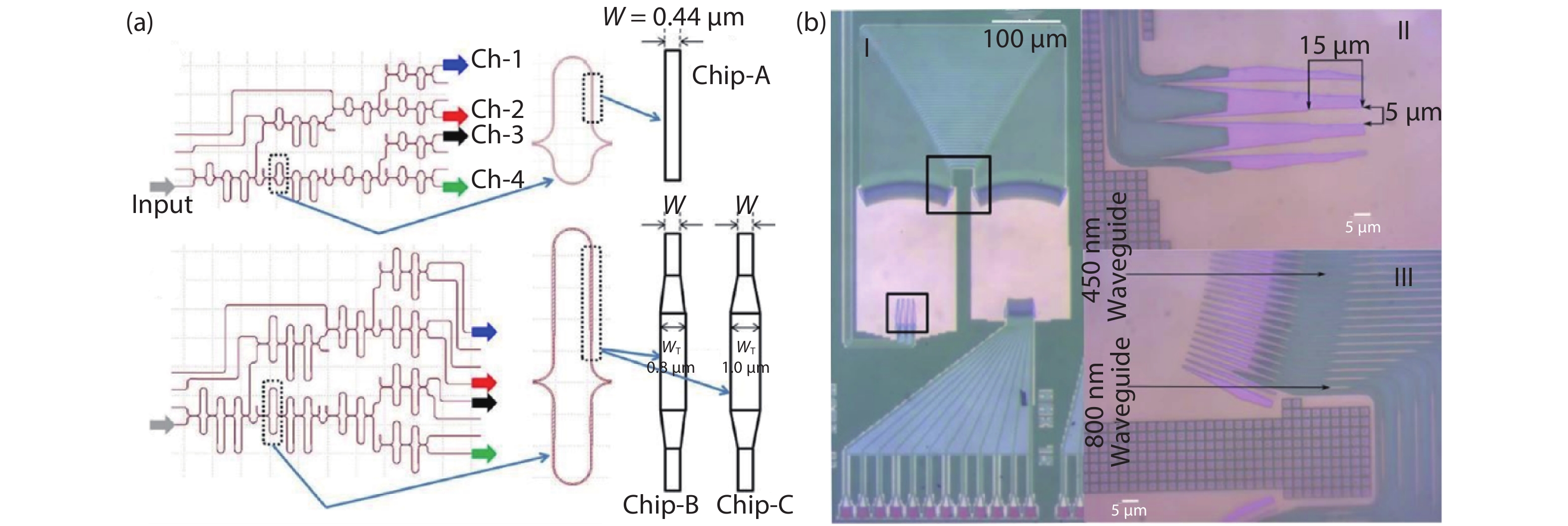
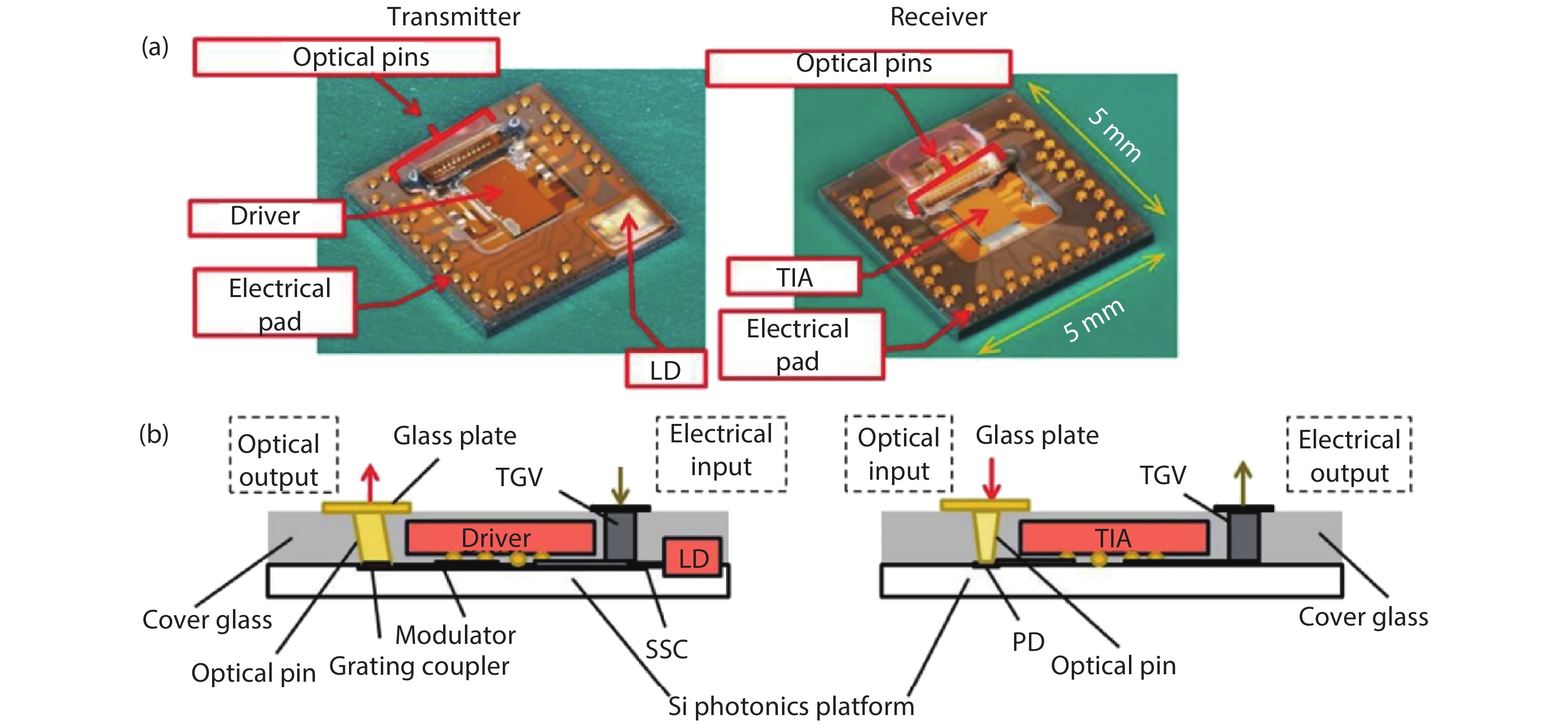
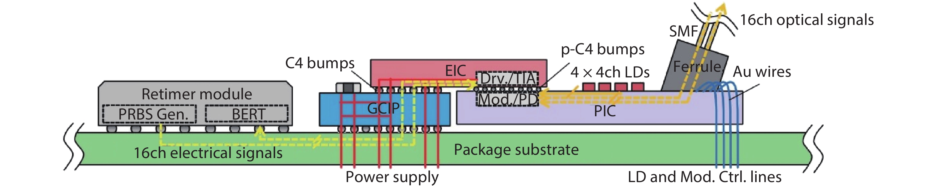
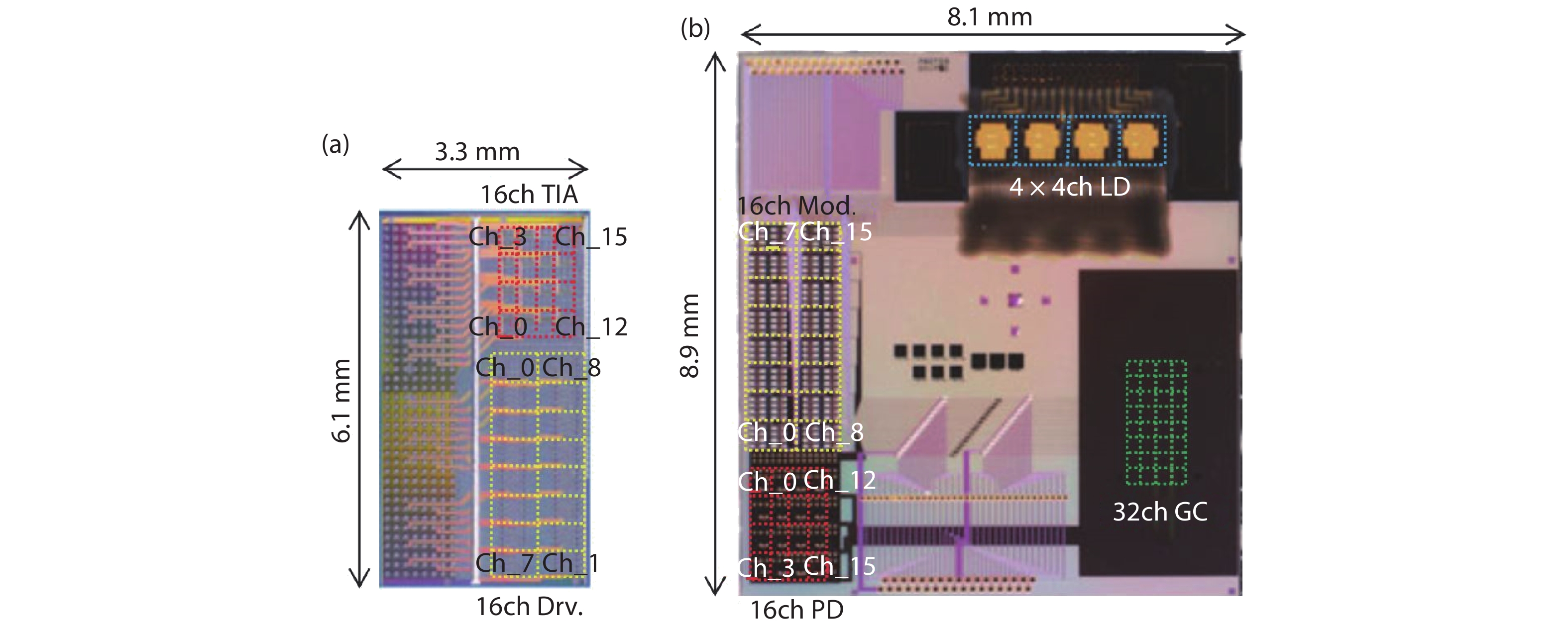
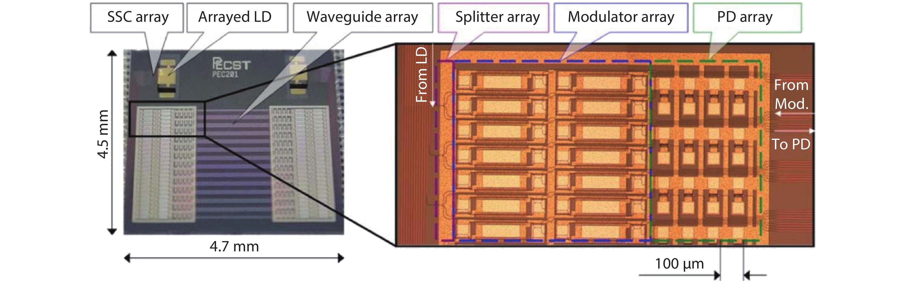
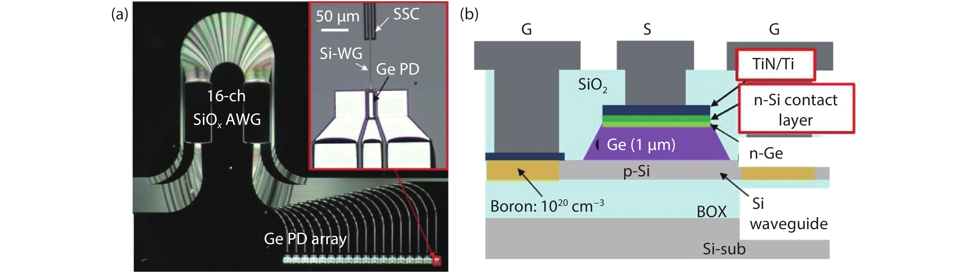
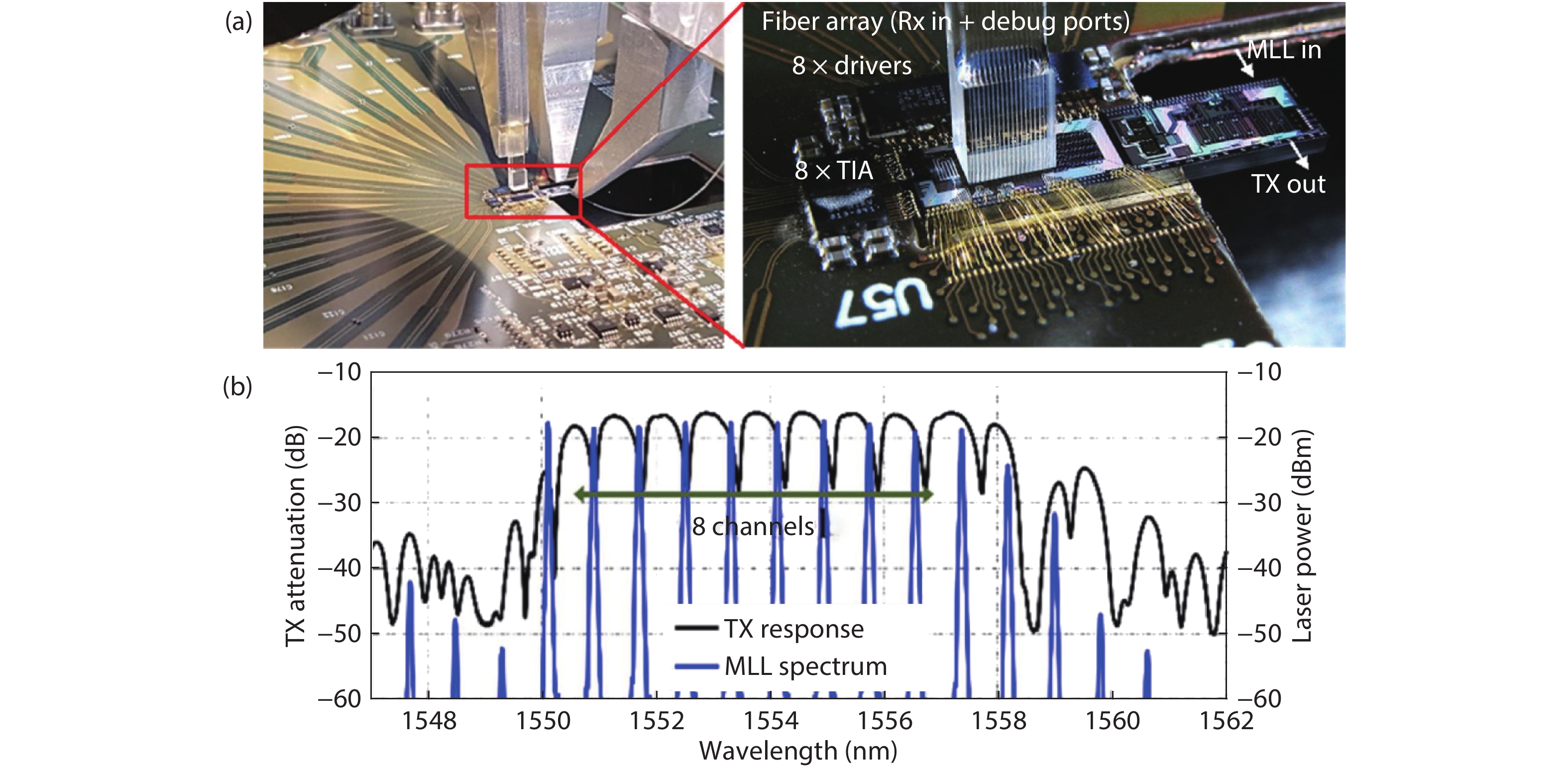
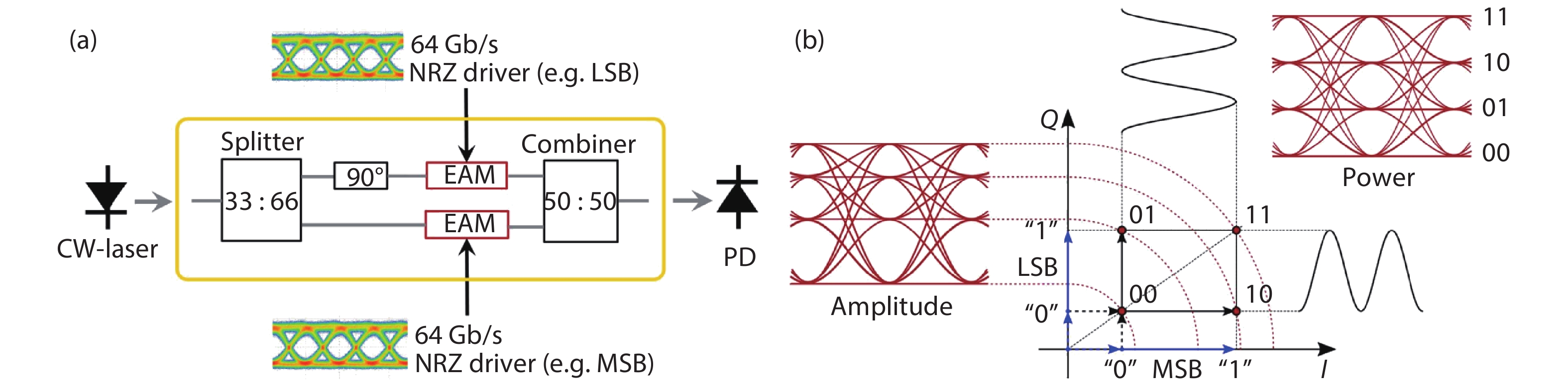
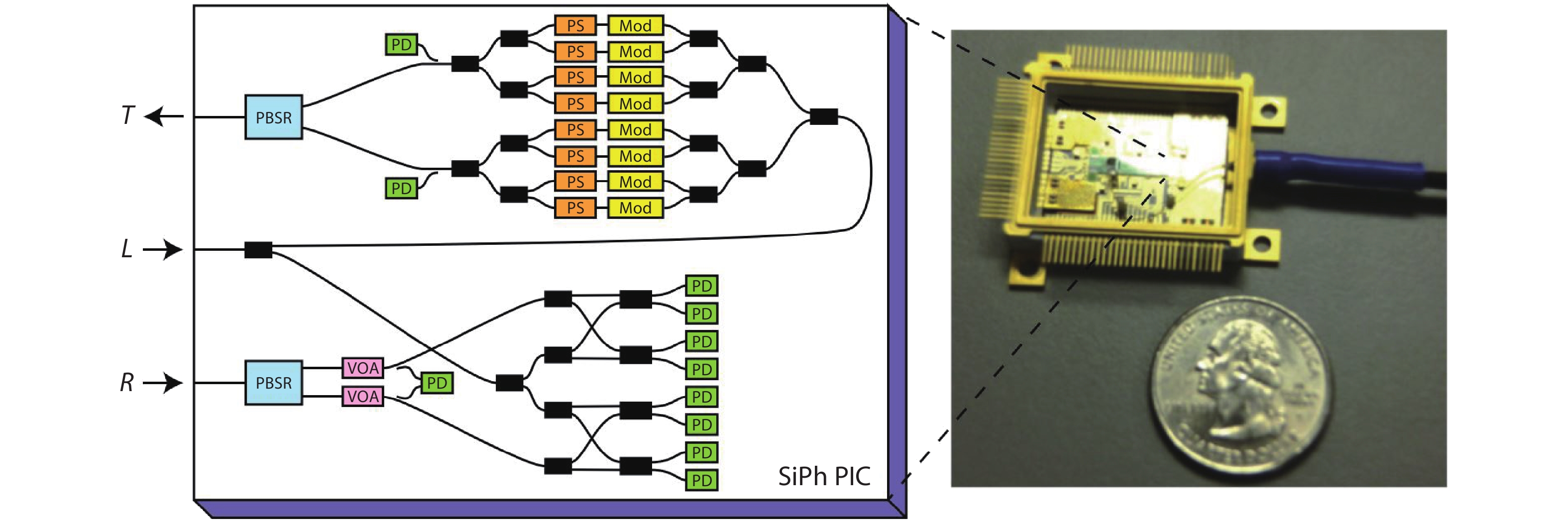
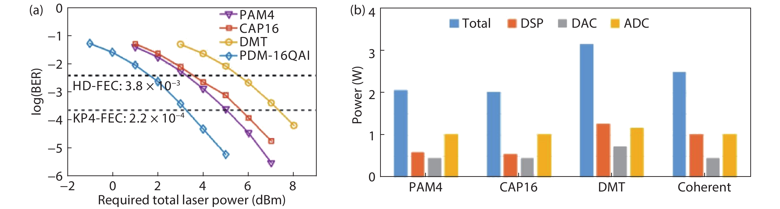
Global data traffic is growing rapidly, and the demand for optoelectronic transceivers applied in data centers (DCs) is also increasing correspondingly. In this review, we first briefly introduce the development of optoelectronics transceivers in DCs, as well as the advantages of silicon photonic chips fabricated by complementary metal oxide semiconductor process. We also summarize the research on the main components in silicon photonic transceivers. In particular, quantum dot lasers have shown great potential as light sources for silicon photonic integration—whether to adopt bonding method or monolithic integration—thanks to their unique advantages over the conventional quantum-well counterparts. Some of the solutions for high-speed optical interconnection in DCs are then discussed. Among them, wavelength division multiplexing and four-level pulse-amplitude modulation have been widely studied and applied. At present, the application of coherent optical communication technology has moved from the backbone network, to the metro network, and then to DCs.


The purpose of this work is to analyze the electrical properties of the metal–semiconductor contact (MSC) in the framework of the theory of complex systems. The effect of inhomogeneity of the different microstructures: polycrystalline, monocrystalline, amorphous metal–semiconductor contact surface is investigated, considering a Schottky diode (SD) as a parallel connection of numerous subdiodes. It has been shown that the polycrystallinity of the metal translates a homogeneous contact into a complex system, which consists of parallel connected numerous elementary contacts having different properties and parameters.


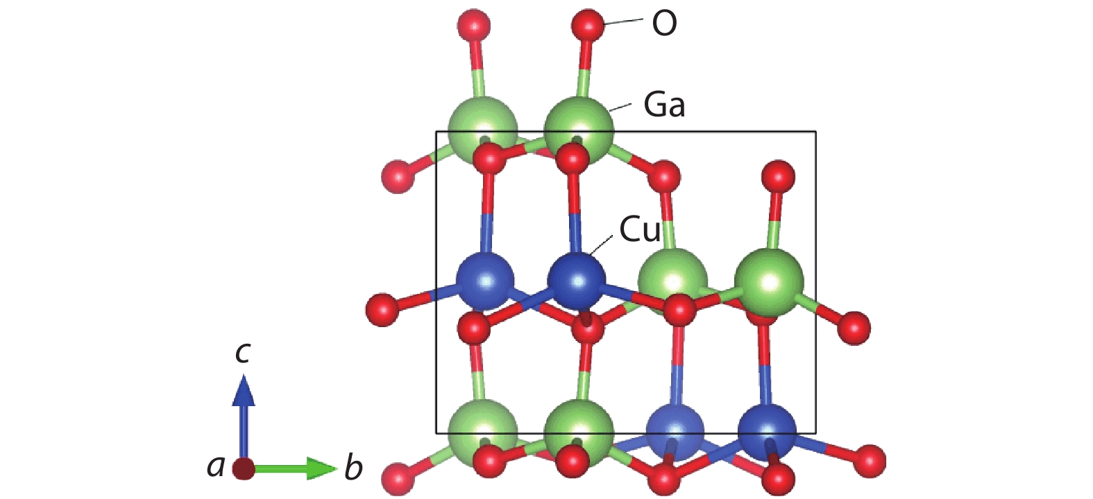
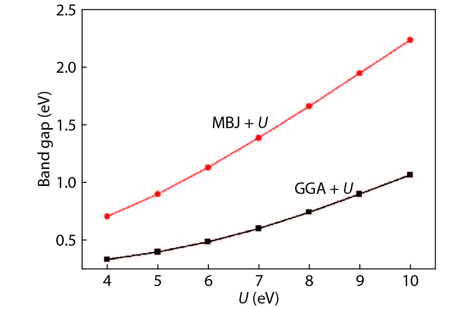
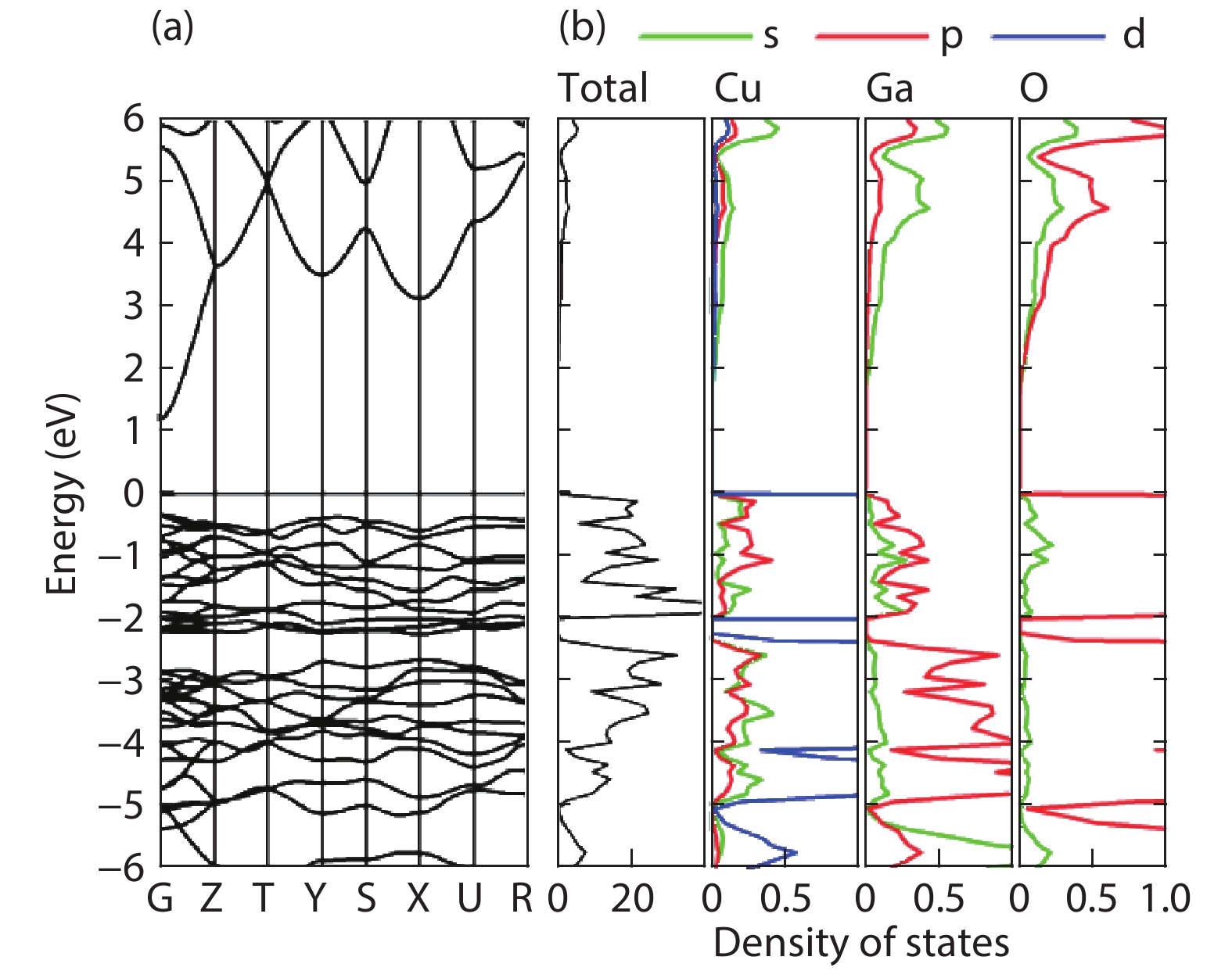
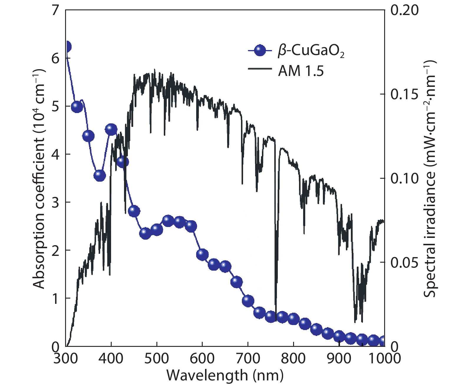
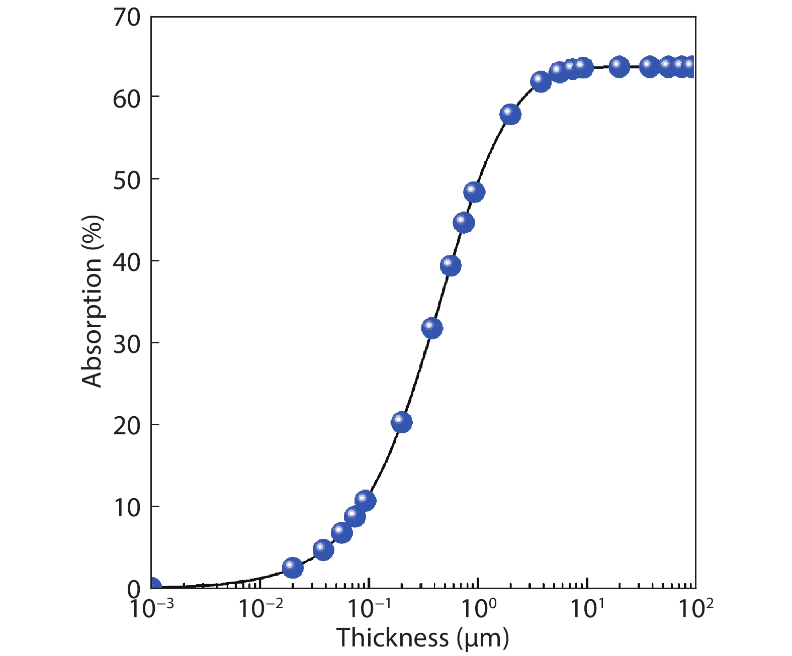
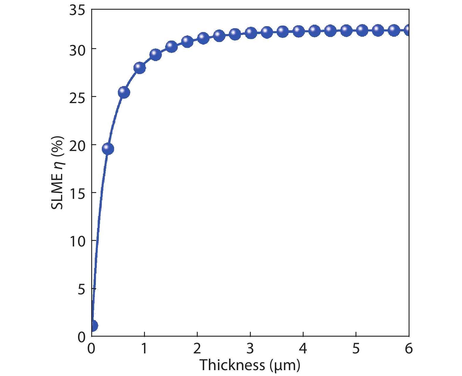
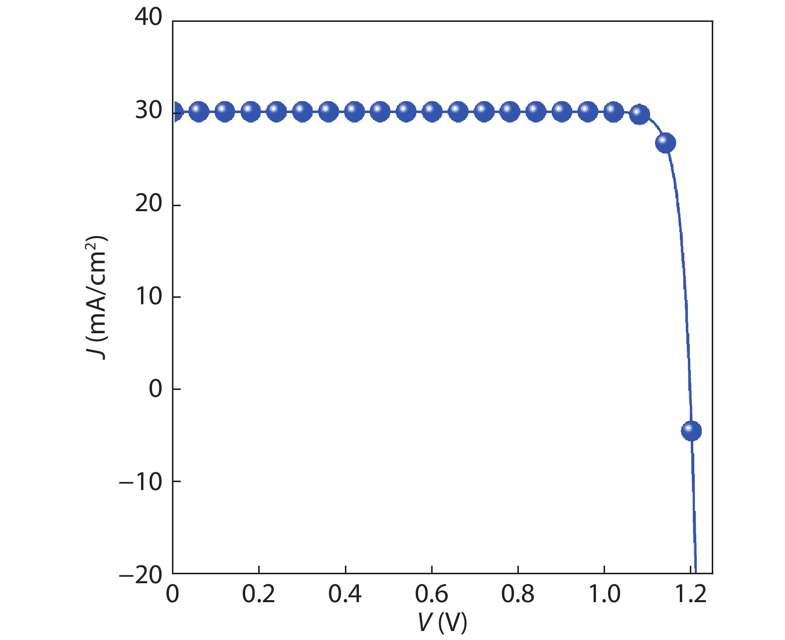
Based on the density functional theory, the energy band and electronic structure of β-CuGaO2 are calculated by the modified Becke-Johnson plus an on-site Coulomb U (MBJ + U) approach in this paper. The calculated results show that the band gap value of β-CuGaO2 obtained by the MBJ + U approach is close to the experimental value. The calculated results of electronic structure indicate that the main properties of the material are determined by the bond between Cu-3d and O-2p energy levels near the valence band of β-CuGaO2, while a weak anti-bond combination is formed mainly by the O-2p energy level and Ga-4s energy level near the bottom of the conduction band of β-CuGaO2. The β-CuGaO2 thin film is predicted to hold excellent photovoltaic performance by analysis of the spectroscopic limited maximum efficiency (SLME) method. At the same time, the calculated maximum photoelectric conversion efficiency of the ideal CuGaO2 solar cell is 32.4%. Relevant conclusions can expand β-CuGaO2 photovoltaic applications.

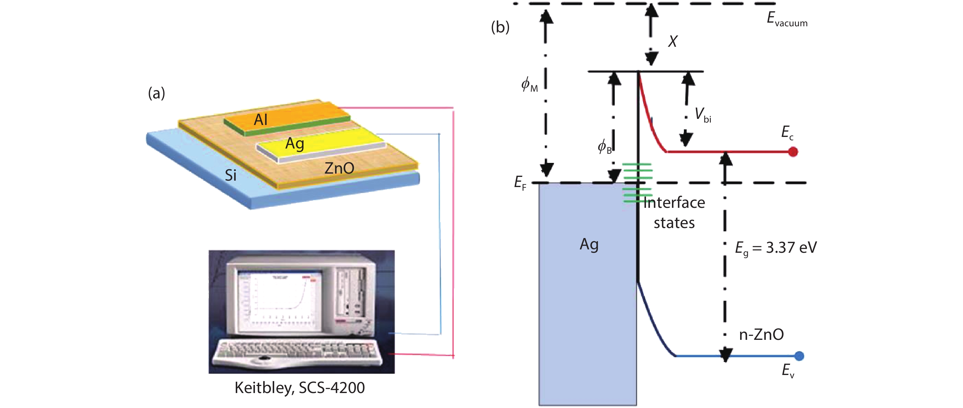
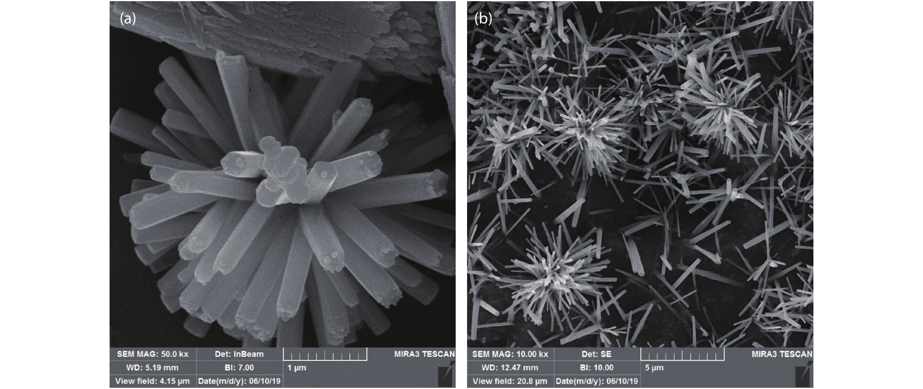
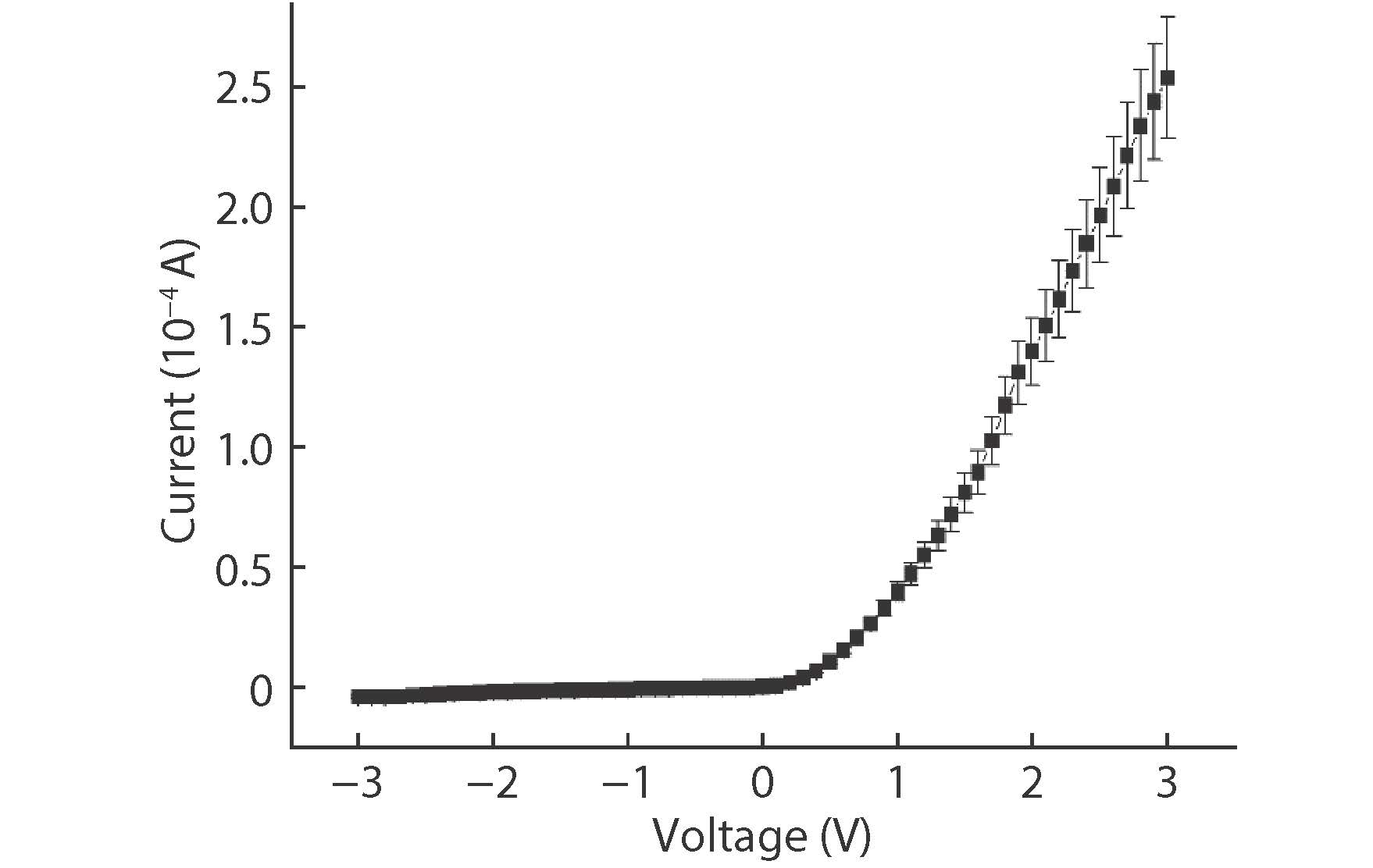
This paper reports the realization of planar Schottky diodes based on nanorod ZnO thin film. The nanorod ZnO thin film was fabricated by hydrothermal technique on boron doped p-type Si (100) substrate. The Ag//ZnO/Al planar diode operating with voltage bias from –3 to 3 V. The I–V characteristics clearly indicate that the devices have rectifying performance. The thermionic emission theory governs the current across the studied Schottky diode. The device achieved a turn-on voltage of 0.9 V, barrier height 0.69 eV and saturation current of 1.2 × 10⁻⁶ A. The diode shows a very large ideality factor (n > > 2) which is attributed to high interface trap concentration. The surface topology was investigated by scanning electron microscope (SEM). The structural properties of the nanostructured ZnO thin film were characterized by X-ray diffraction (XRD). The SEM images reveal that the ZnO nanorods grow perpendicular to the substrate with uniformity and high density. The XRD pattern illustrates the dominant peak appearing at (002). This intense peak indicates the c-axis orientated phase of the wurtzite ZnO structure. It demonstrates that the crystals grow uniformly perpendicular to the substrate surface in good agreement with the SEM images.


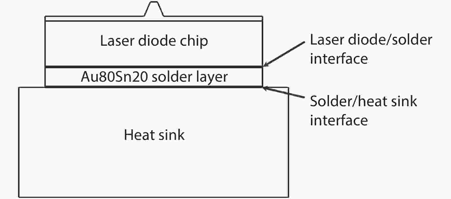
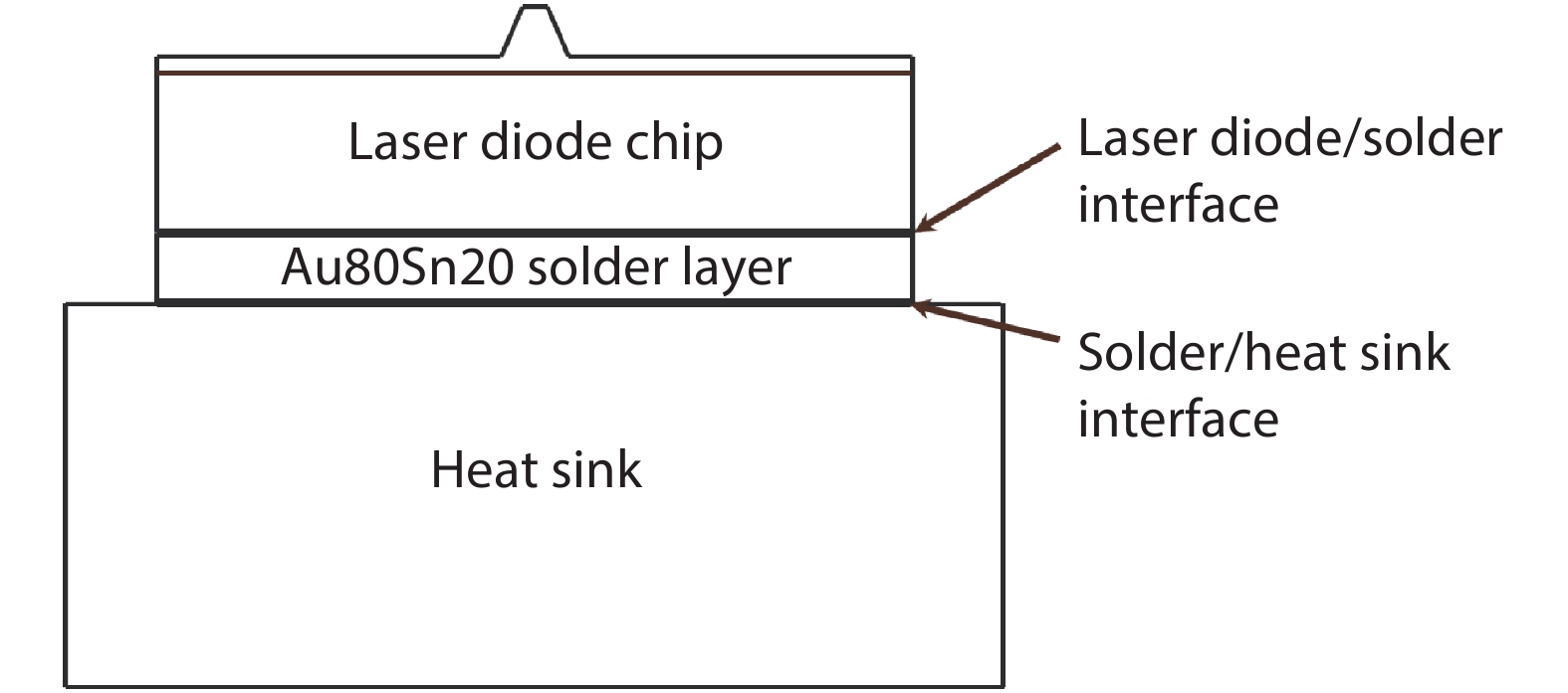
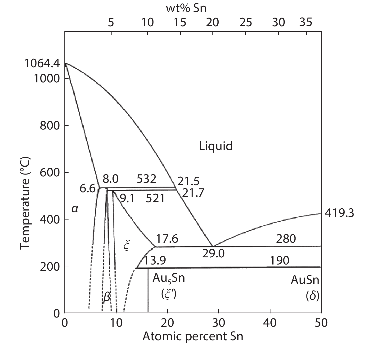
Au80Sn20 alloy is a widely used solder for laser diode packaging. In this paper, the thermal resistance of GaN-based blue laser diodes packaged in TO56 cans were measured by the forward voltage method. The microstructures of Au80Sn20 solder were then investigated to understand the reason for the difference in thermal resistance. It was found that the microstructure with a higher content of Au-rich phase in the center of the solder and a lower content of (Au,Ni)Sn phase at the interface of the solder/heat sink resulted in lower thermal resistance. This is attributed to the lower thermal resistance of Au-rich phase and higher thermal resistance of (Au,Ni)Sn phase.


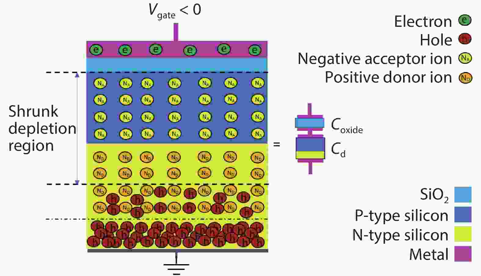
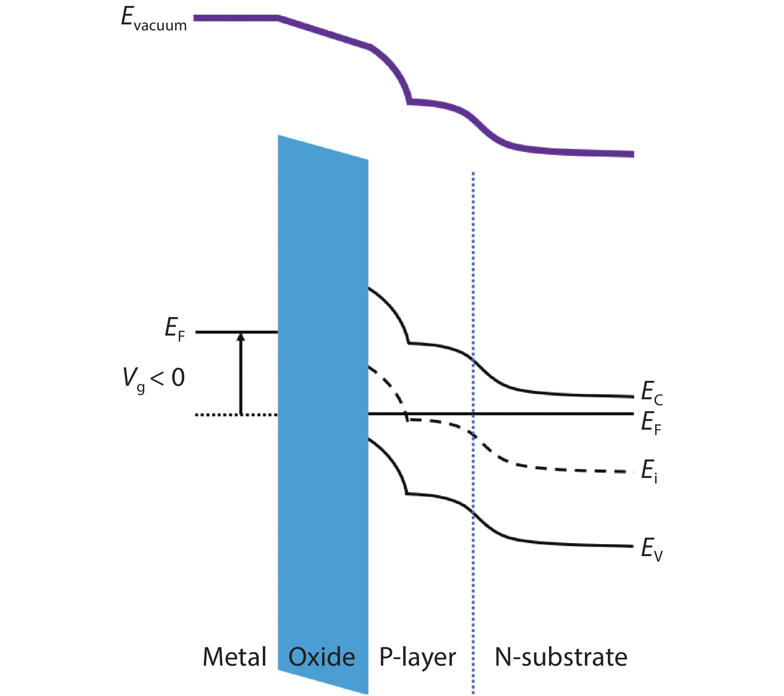
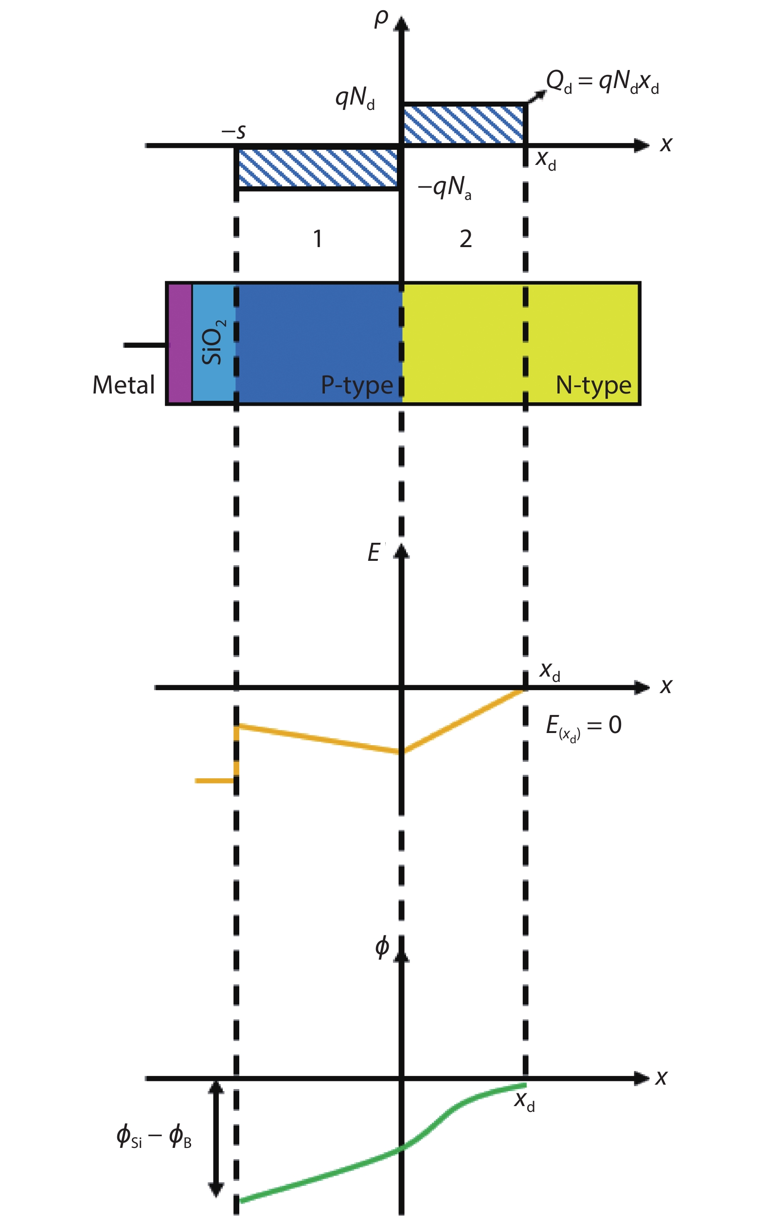
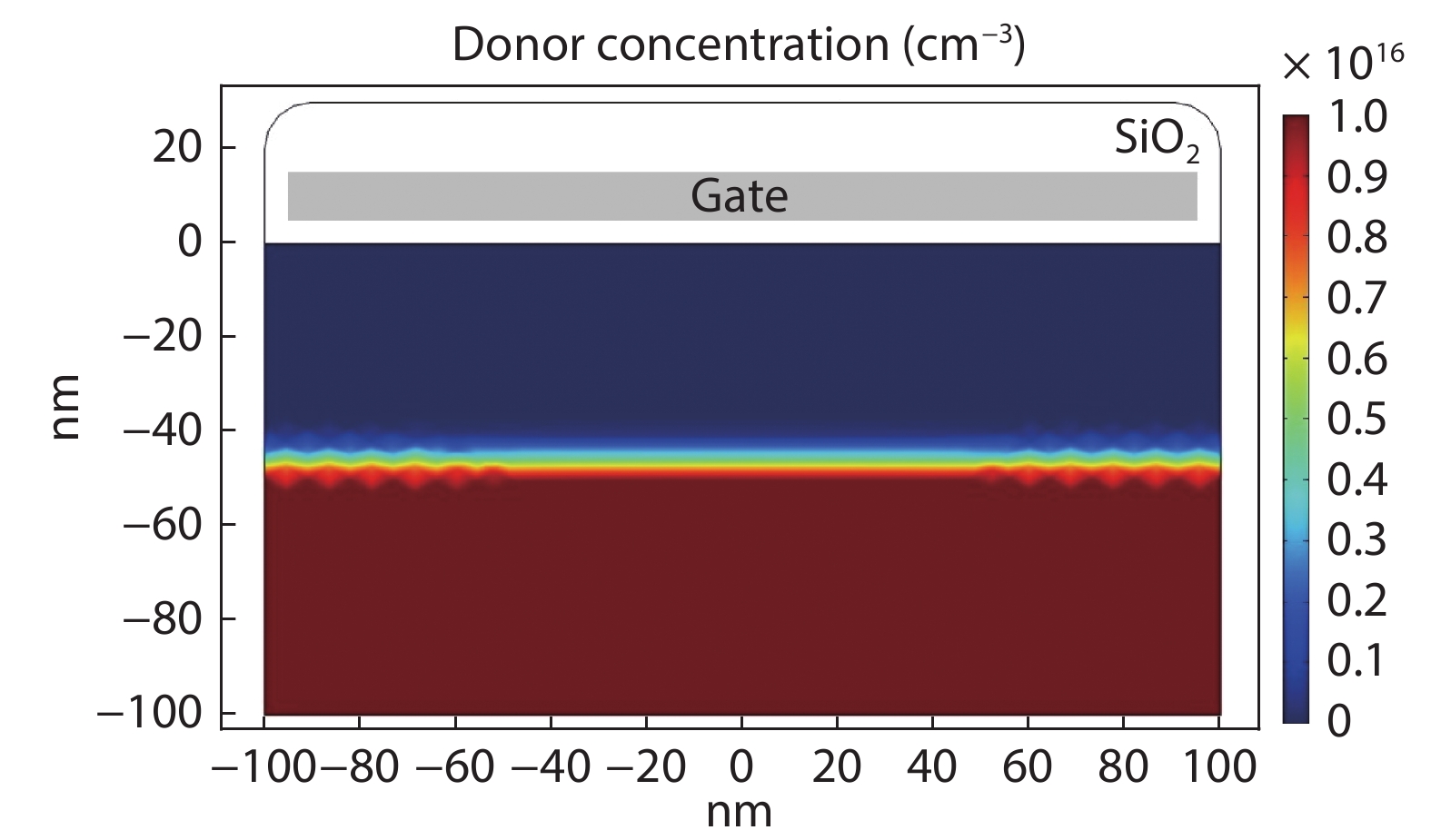
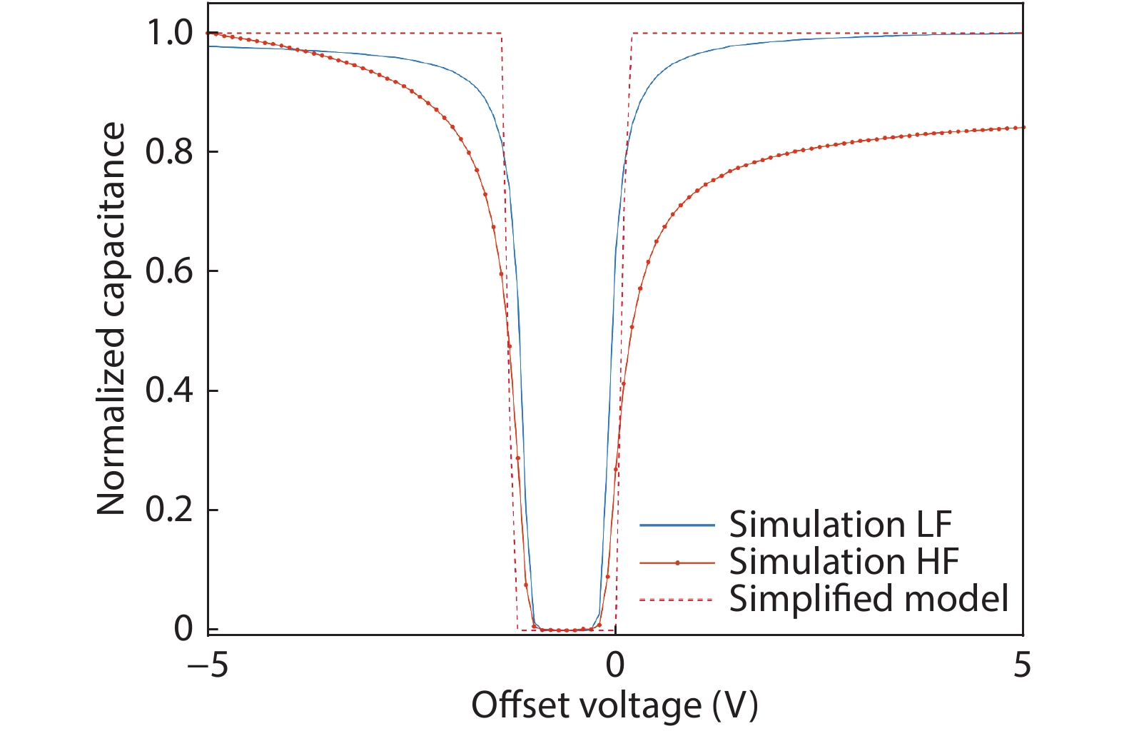
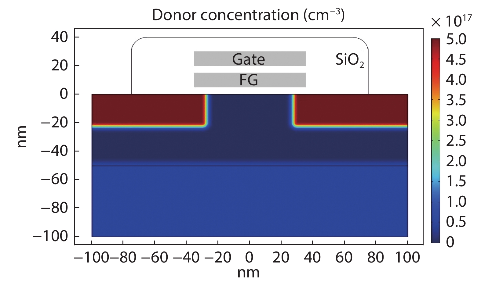
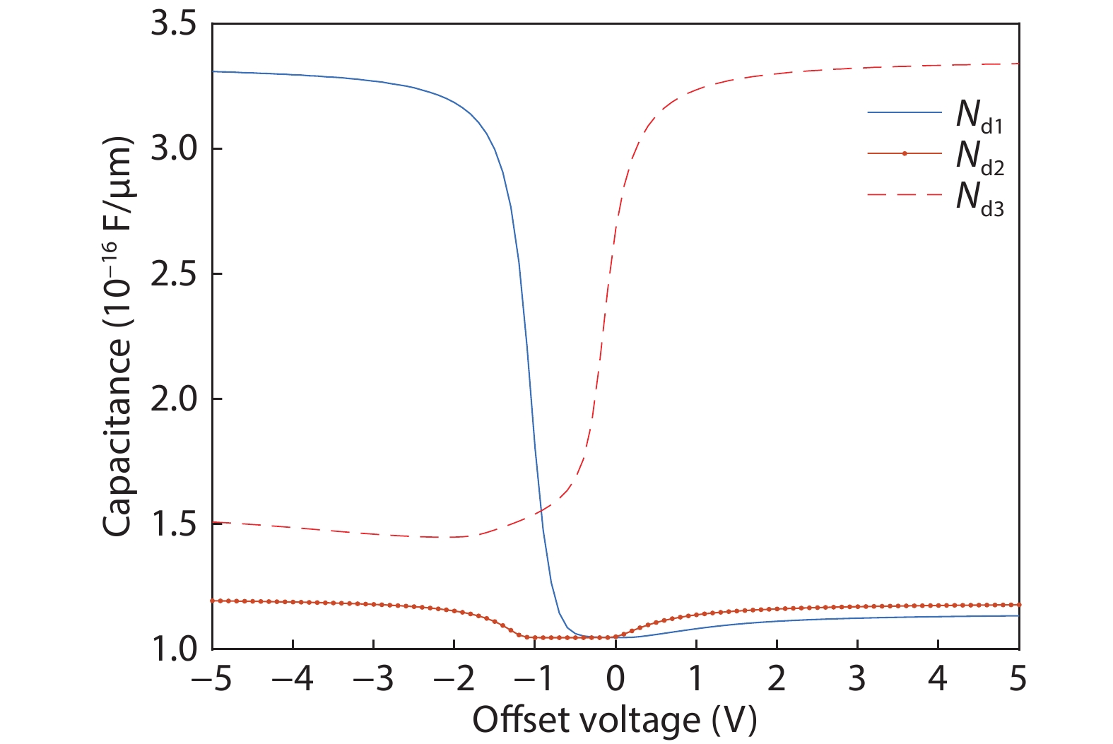
This study proposes a new generation of floating gate transistors (FGT) with a novel built-in security feature. The new device has applications in guarding the IC chips against the current reverse engineering techniques, including scanning capacitance microscopy (SCM). The SCM measures the change in the C–V characteristic of the device as a result of placing a minute amount of charge on the floating gate, even in nano-meter scales. The proposed design only adds a simple processing step to the conventional FGT by adding an oppositely doped implanted layer to the substrate. This new structure was first analyzed theoretically and then a two-dimensional model was extracted to represent its C–V characteristic. Furthermore, this model was verified with a simulation. In addition, the C–V characteristics relevant to the SCM measurement of both conventional and the new designed FGT were compared to discuss the effectiveness of the added layer in masking the state of the transistor. The effect of change in doping concentration of the implanted layer on the C–V characteristics was also investigated. Finally, the feasibility of the proposed design was examined by comparing its I–V characteristics with the traditional FGT.


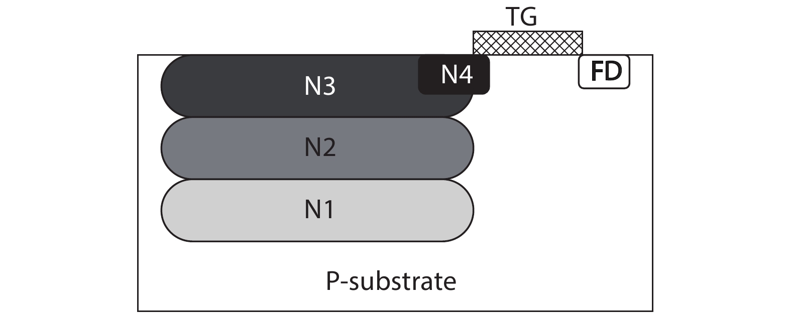
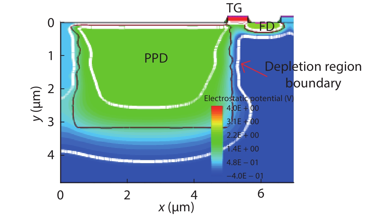
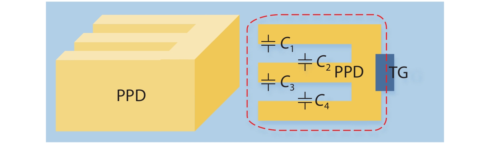
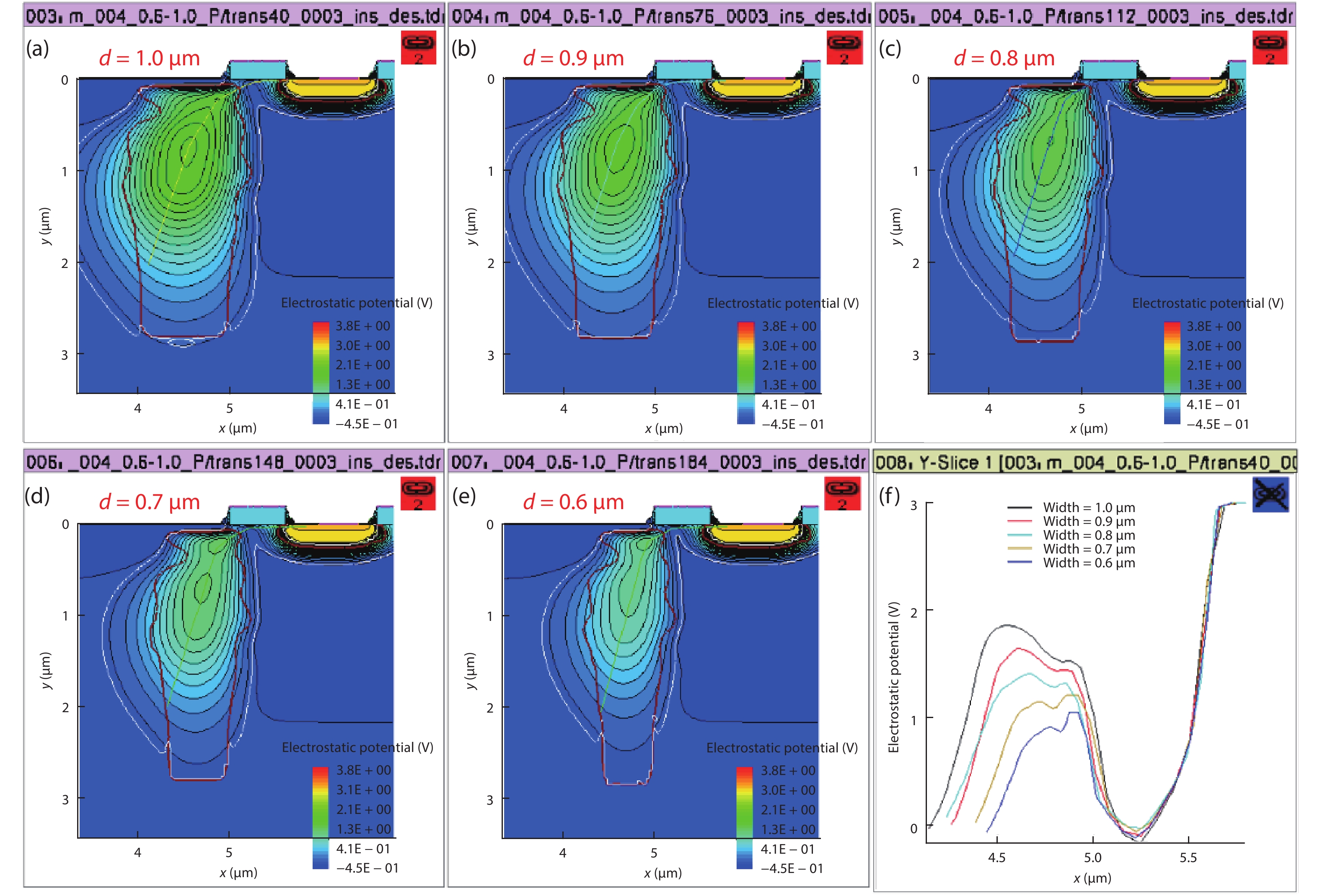
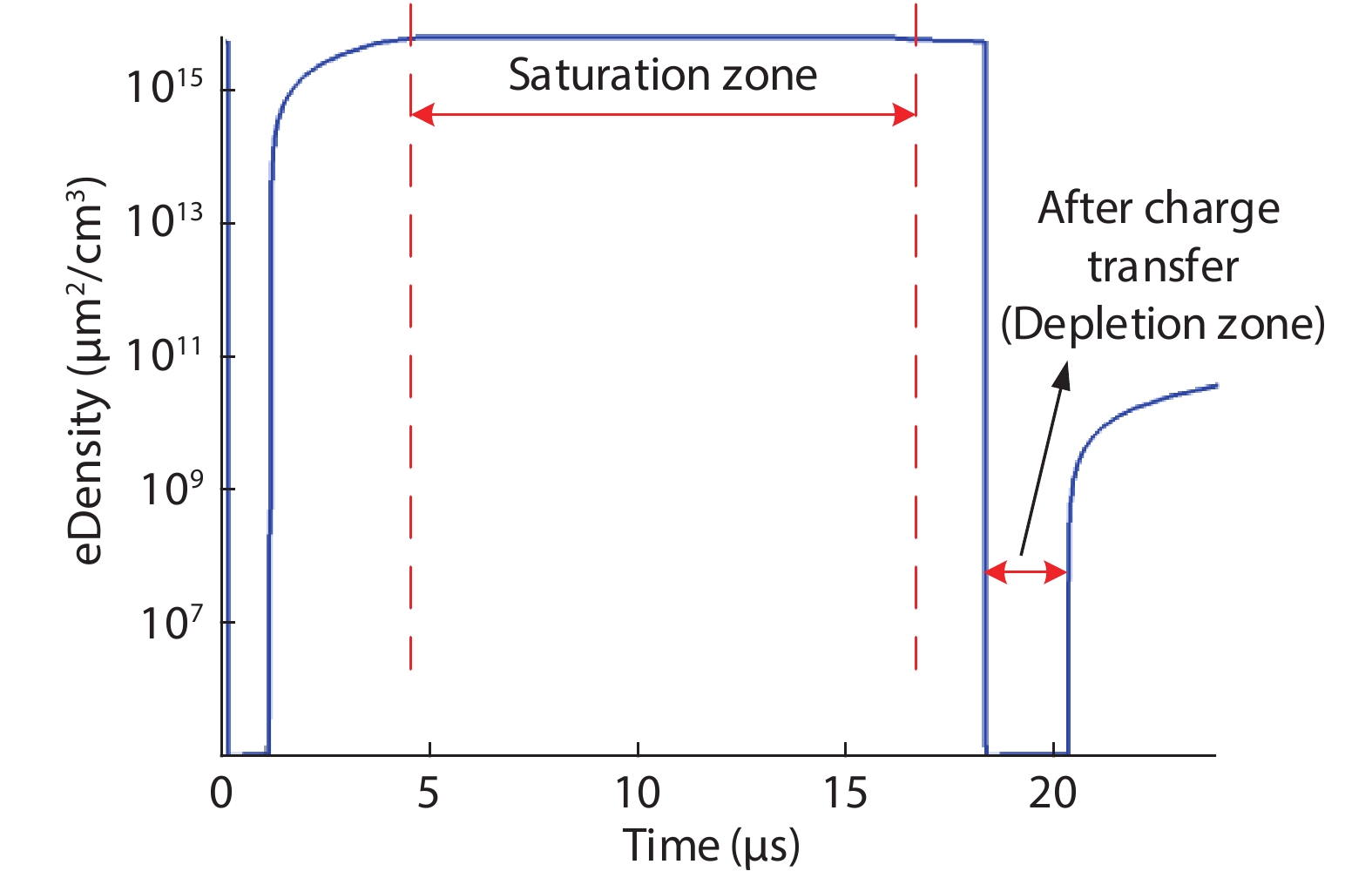
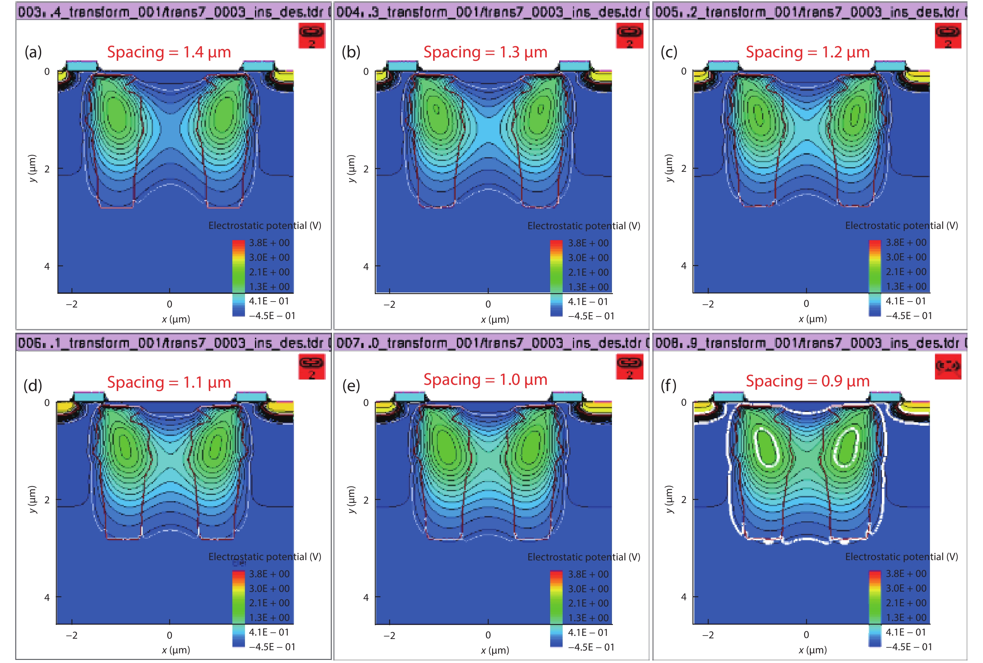
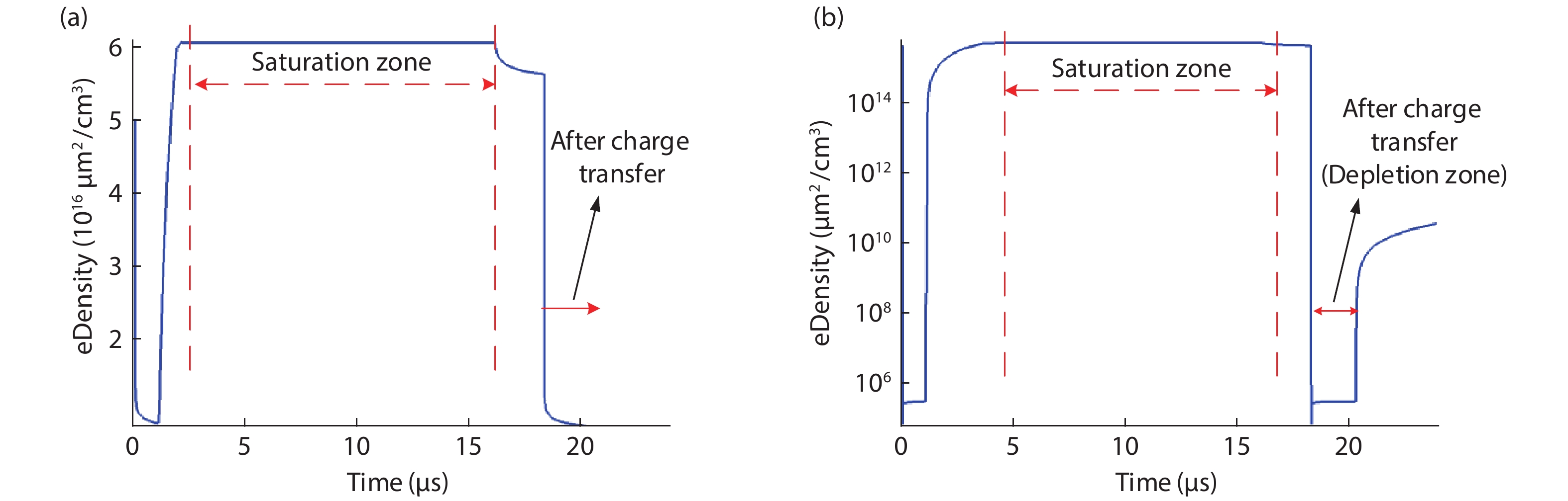
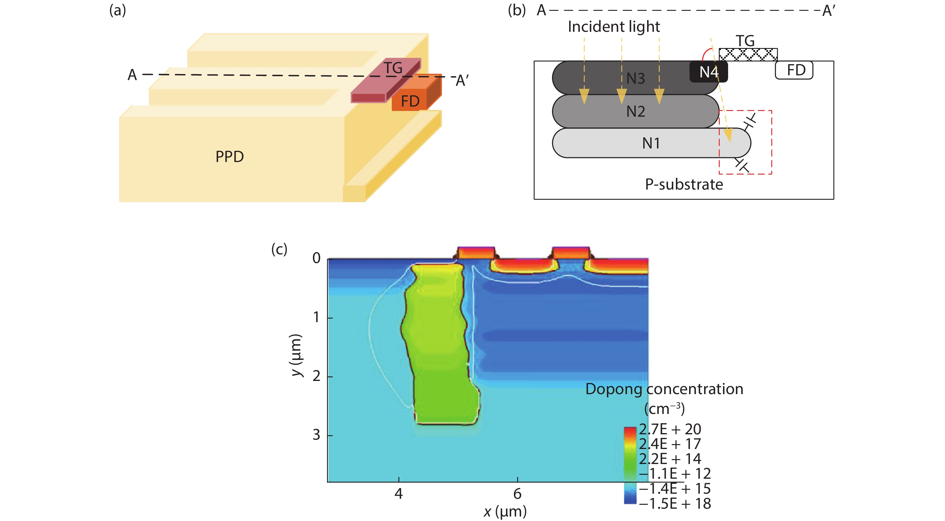
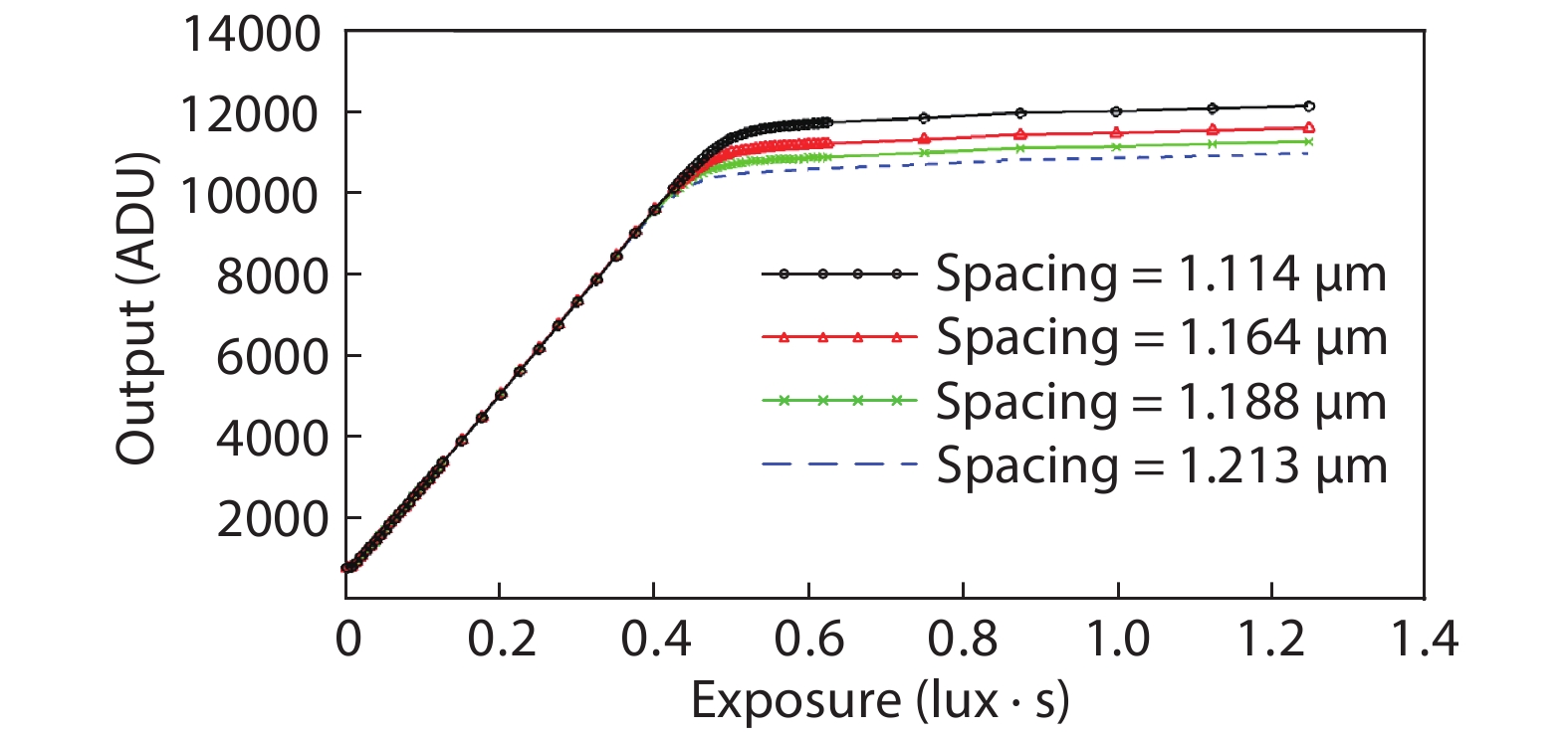
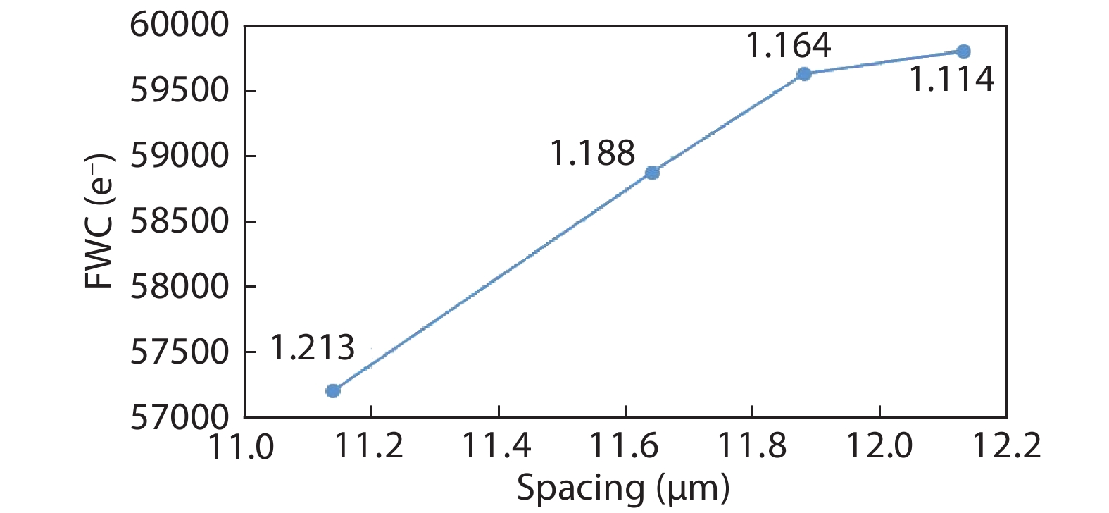
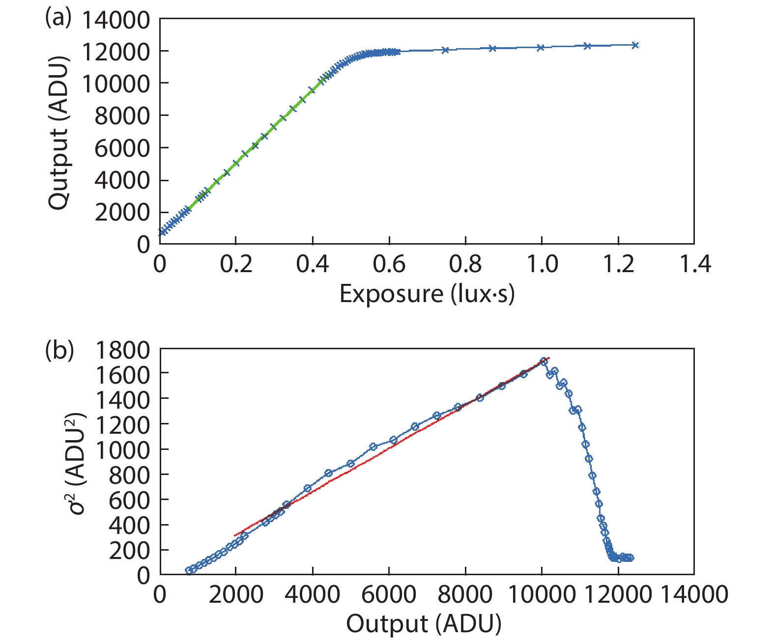
To improve the full-well capacity and linear dynamic range of CMOS image sensor, a special finger-shaped pinned photodiode (PPD) is designed. In terms of process, the first N-type ion implantation of the PPD N buried layer is extended under the transfer gate, thereby increasing the PPD capacitance. Based on TCAD simulation, the width and spacing of PPD were precisely adjusted. A high full-well capacity pixel design with a pixel size of 6 × 6 μm2 is realized based on the 0.18 μm CMOS process. The simulation results indicate that the pixel with the above structure and process has a depletion depth of 2.8 μm and a charge transfer efficiency of 100%. The measurement results of the test chip show that the full-well capacity can reach 68650e–. Compared with the conventional structure, the proposed PPD structure can effectively improve the full well capacity of the pixel.


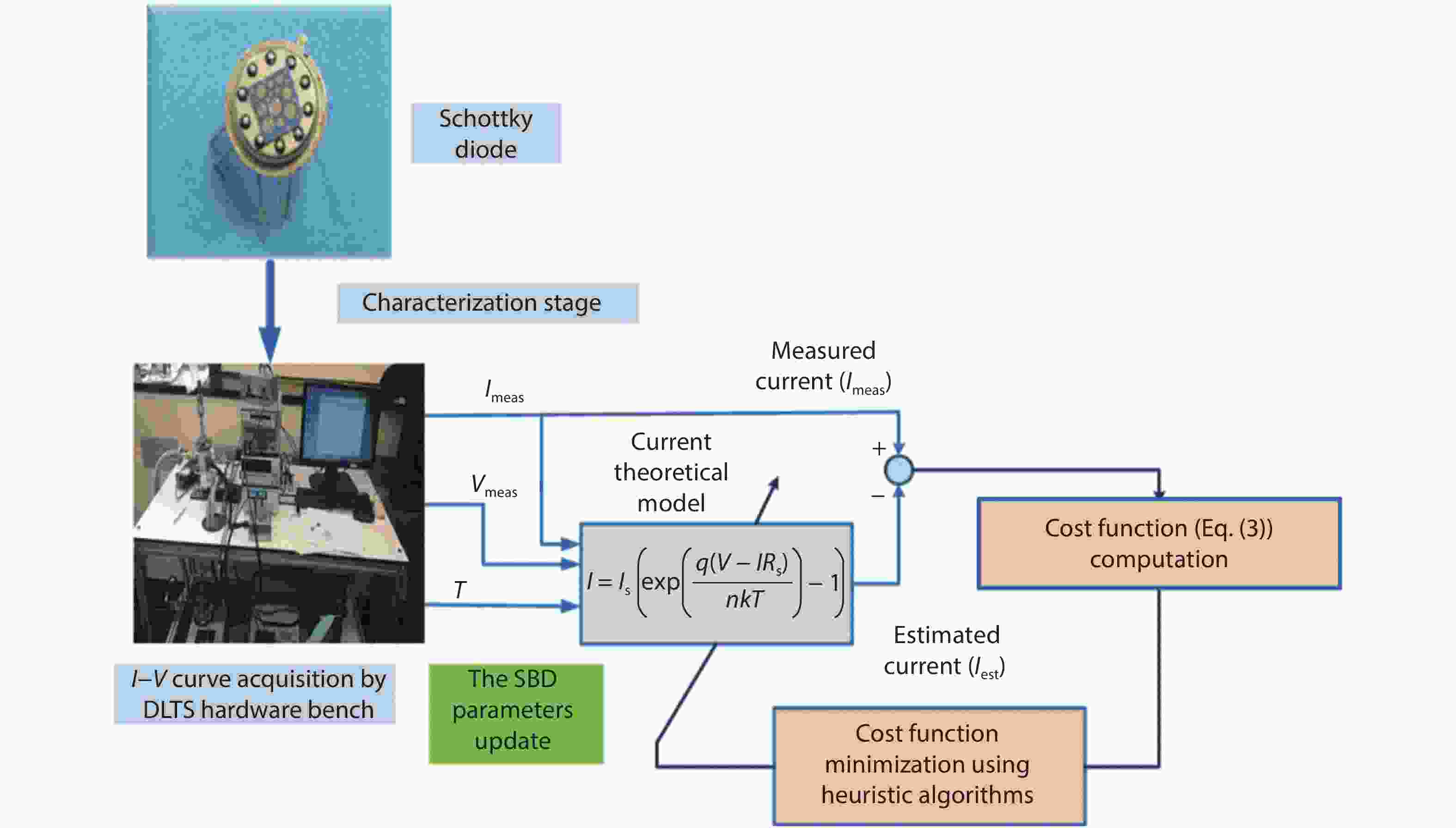
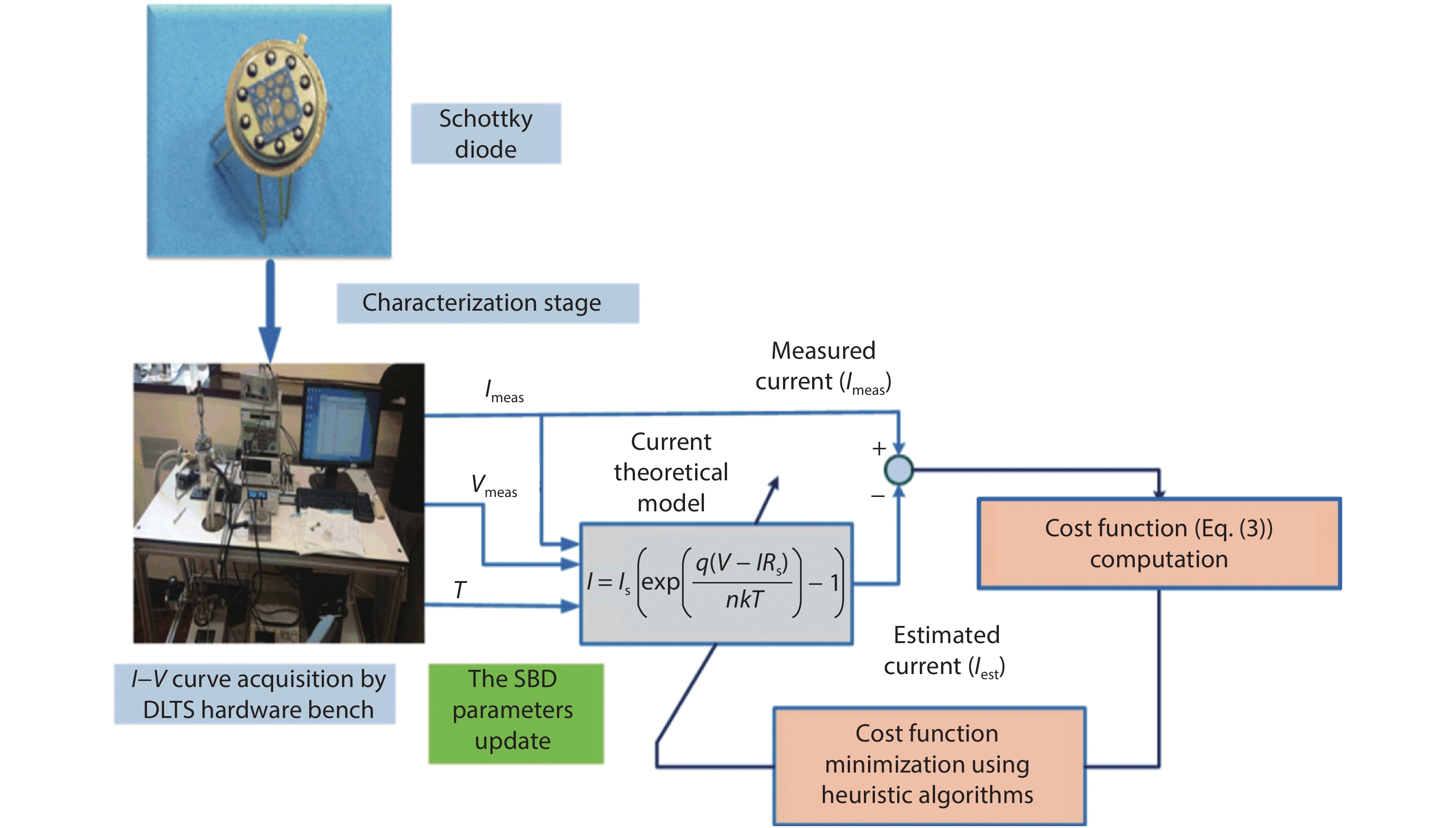
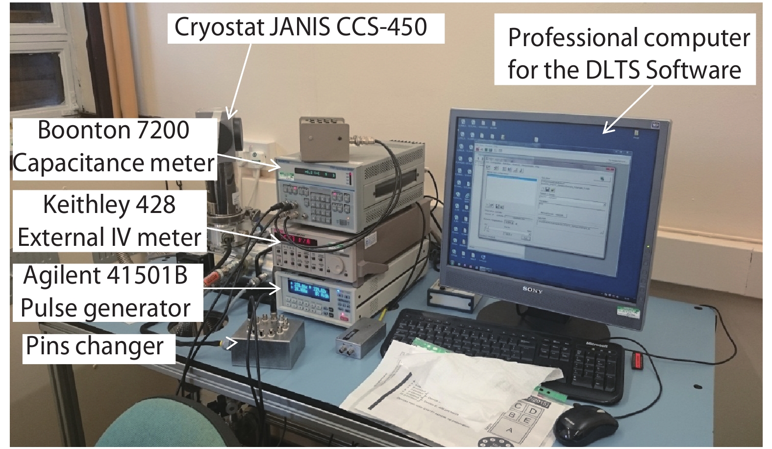
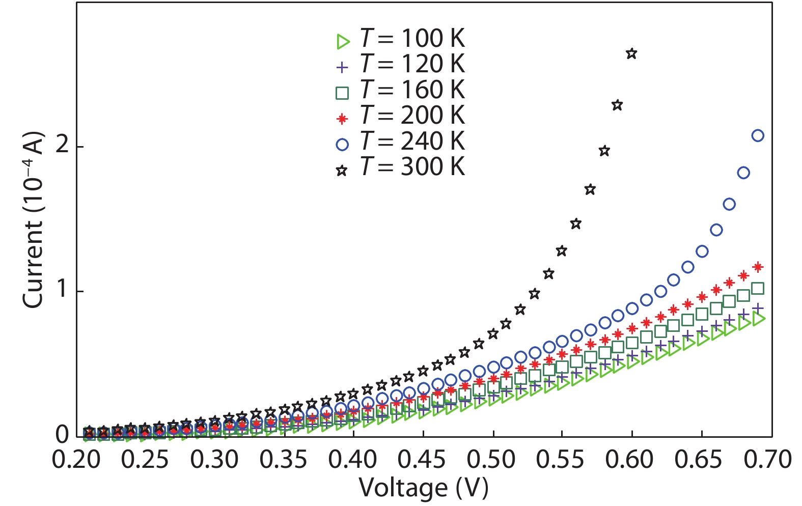
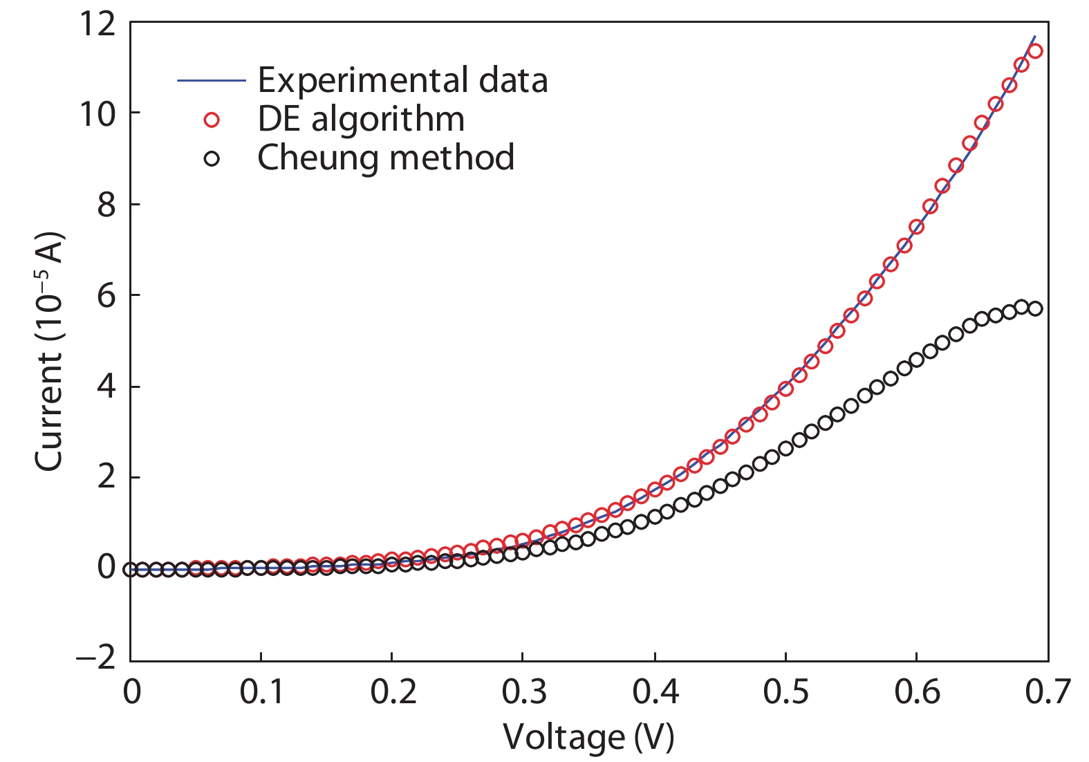
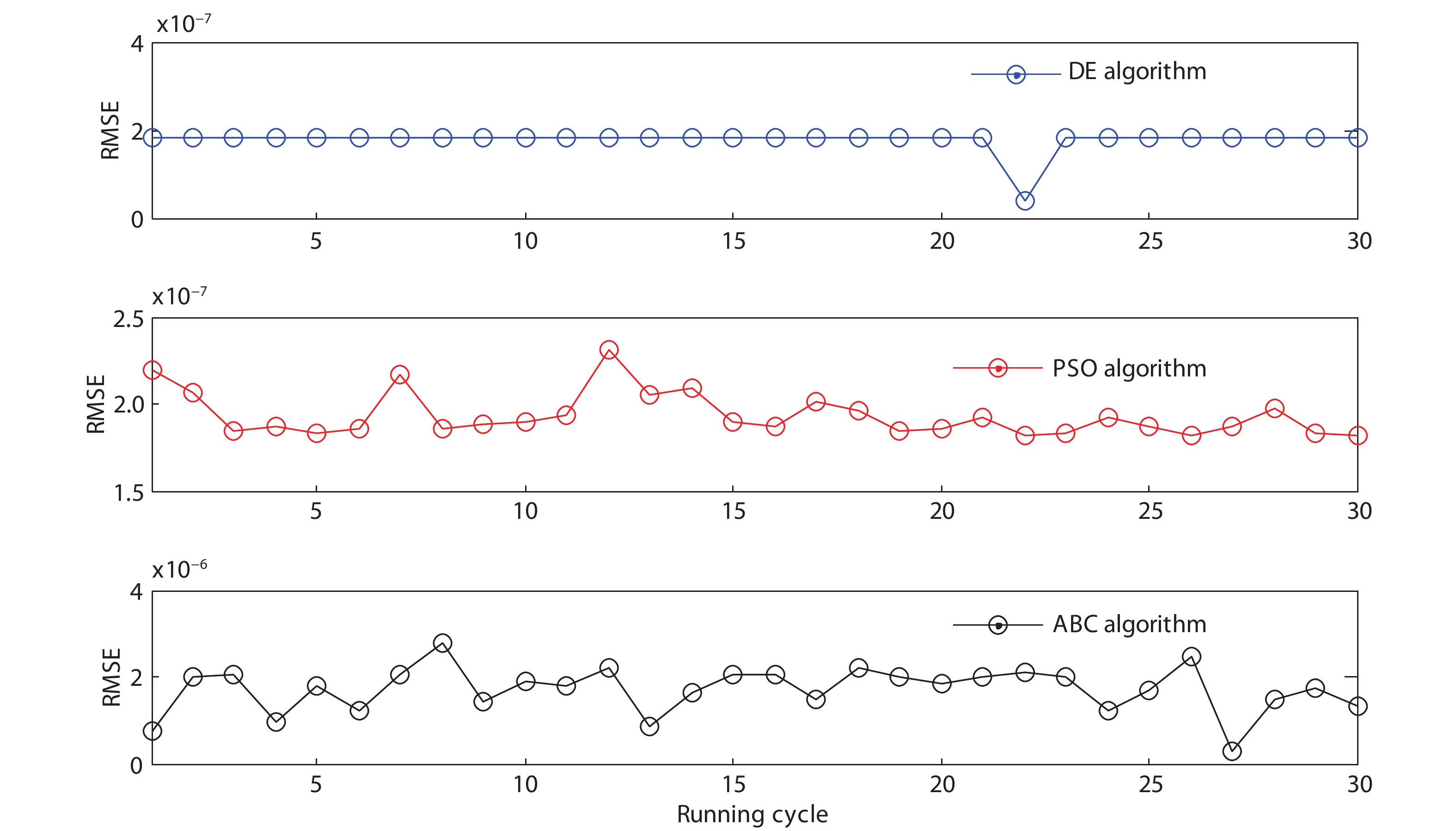
In this work, forward current voltage characteristics for multi-quantum wells Al0.33Ga0.67As Schottky diode were measured at temperature ranges from 100 to 300 K. The main parameters of this Schottky diode, such as the ideality factor, barrier height, series resistance and saturation current, have been extracted using both analytical and heuristics methods. Differential evolution (DE), particle swarm optimization (PSO) and artificial bee colony (ABC) have been chosen as candidate heuristics algorithms, while Cheung technic was selected as analytical extraction method. The obtained results show clearly the high performance of DE algorithms in terms of parameters accuracy, convergence speed and robustness.


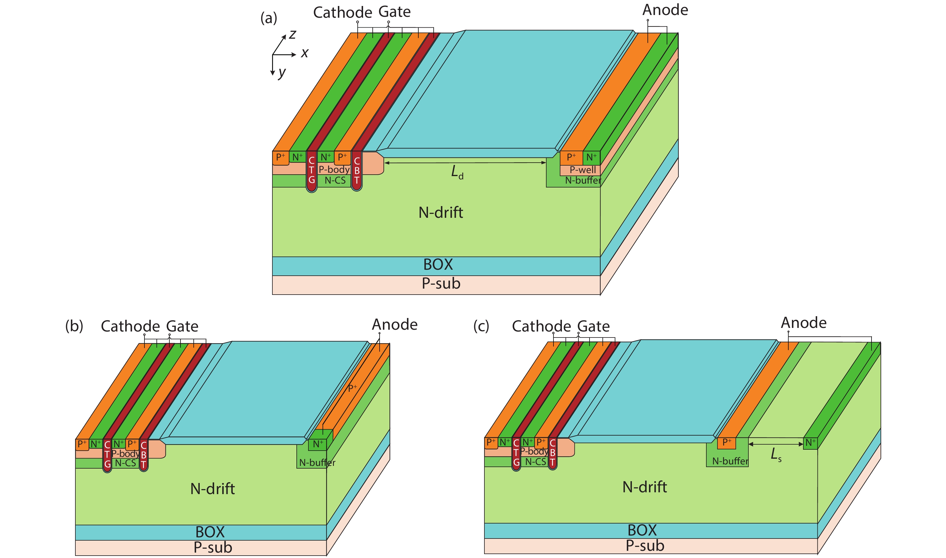
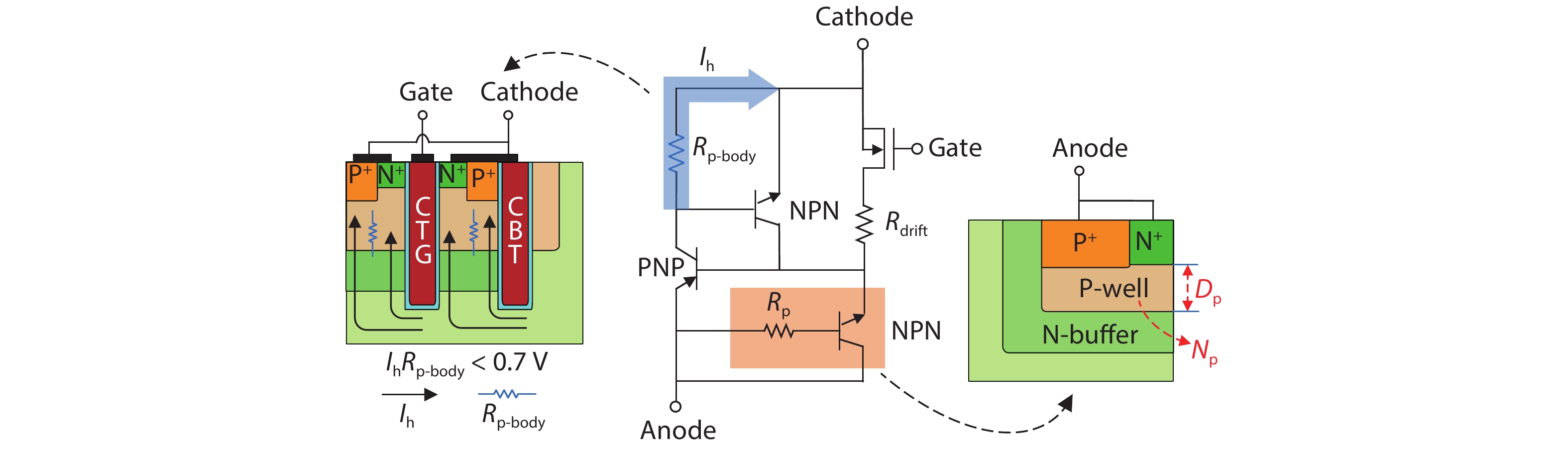
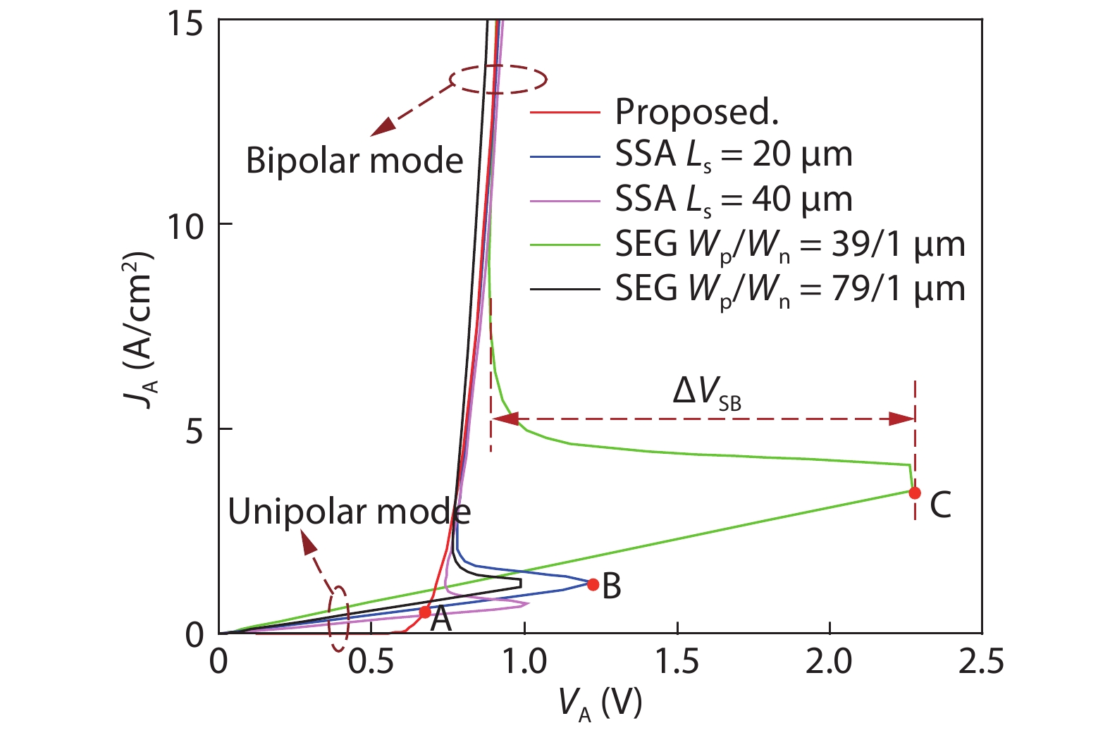
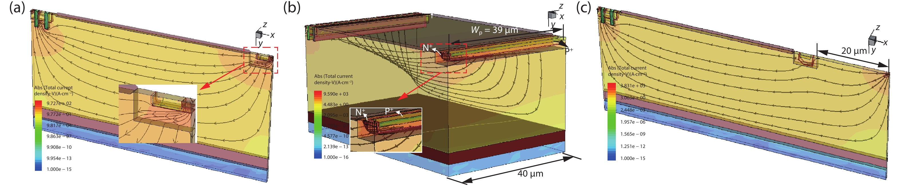
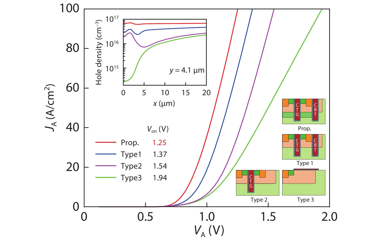
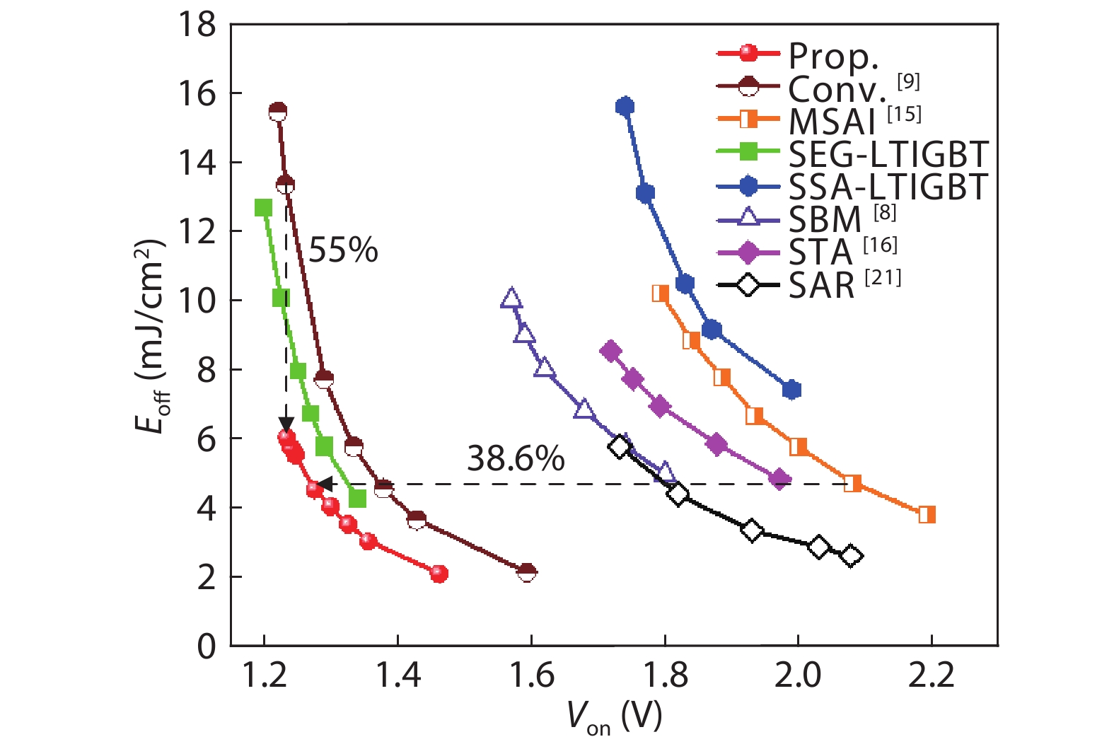
A novel 600 V snapback-free high-speed silicon-on-insulator lateral insulated gate bipolar transistor is proposed and investigated by simulation. The proposed device features an embedded NPN structure at the anode side, and double trenches together with an N-type carrier storage (N-CS) layer at the cathode side, named DT-NPN LIGBT. The NPN structure not only acts as an electron barrier to eliminate the snapback effect in the on-state within a smaller cell pitch but also provides an extra electron extracting path during the turn-off stage to decrease the turnoff loss (Eoff). The double cathode trenches and N-CS layer hinder the hole from being extracted by the cathode quickly. They then enhance carrier storing effect and lead to a reduced on-state voltage drop (Von). The latch-up immunity is improved by the double cathode trenches. Hence, the DT-NPN LIGBT obtains a superior tradeoff between the Von and Eoff. Additionally, the DT-NPN LIGBT exhibits an improved blocking capability and weak dependence of breakdown voltage (BV) on the P+ anode doping concentration because the NPN structure suppresses triggering the PNP transistor. The proposed LIGBT reduces the Eoff by 55% at the same Von, and improves the BV by 7.3% compared to the conventional LIGBT.


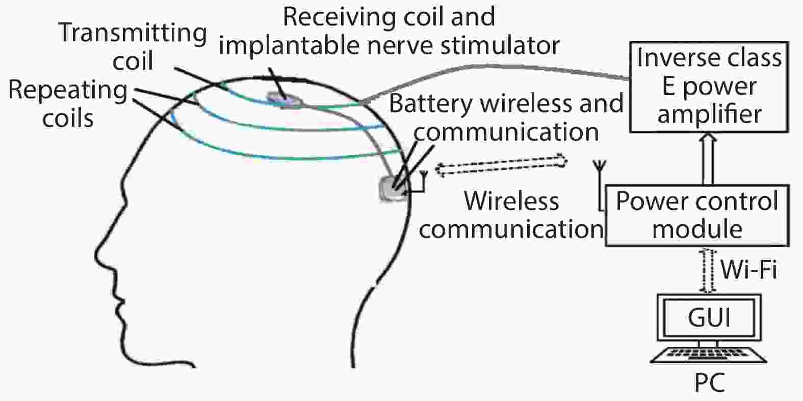
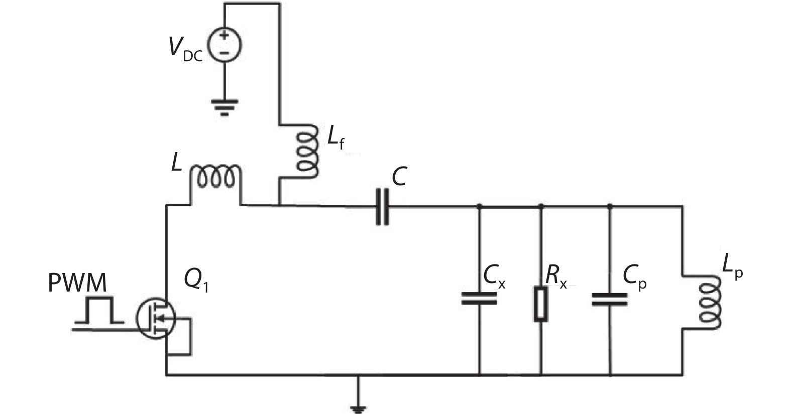
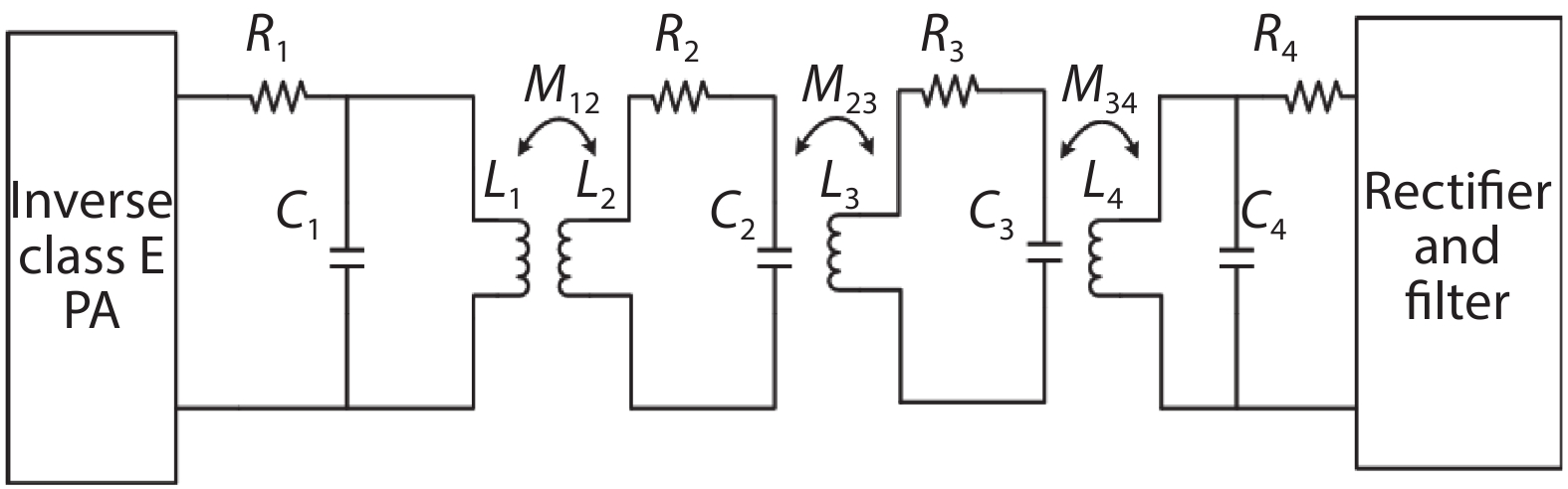
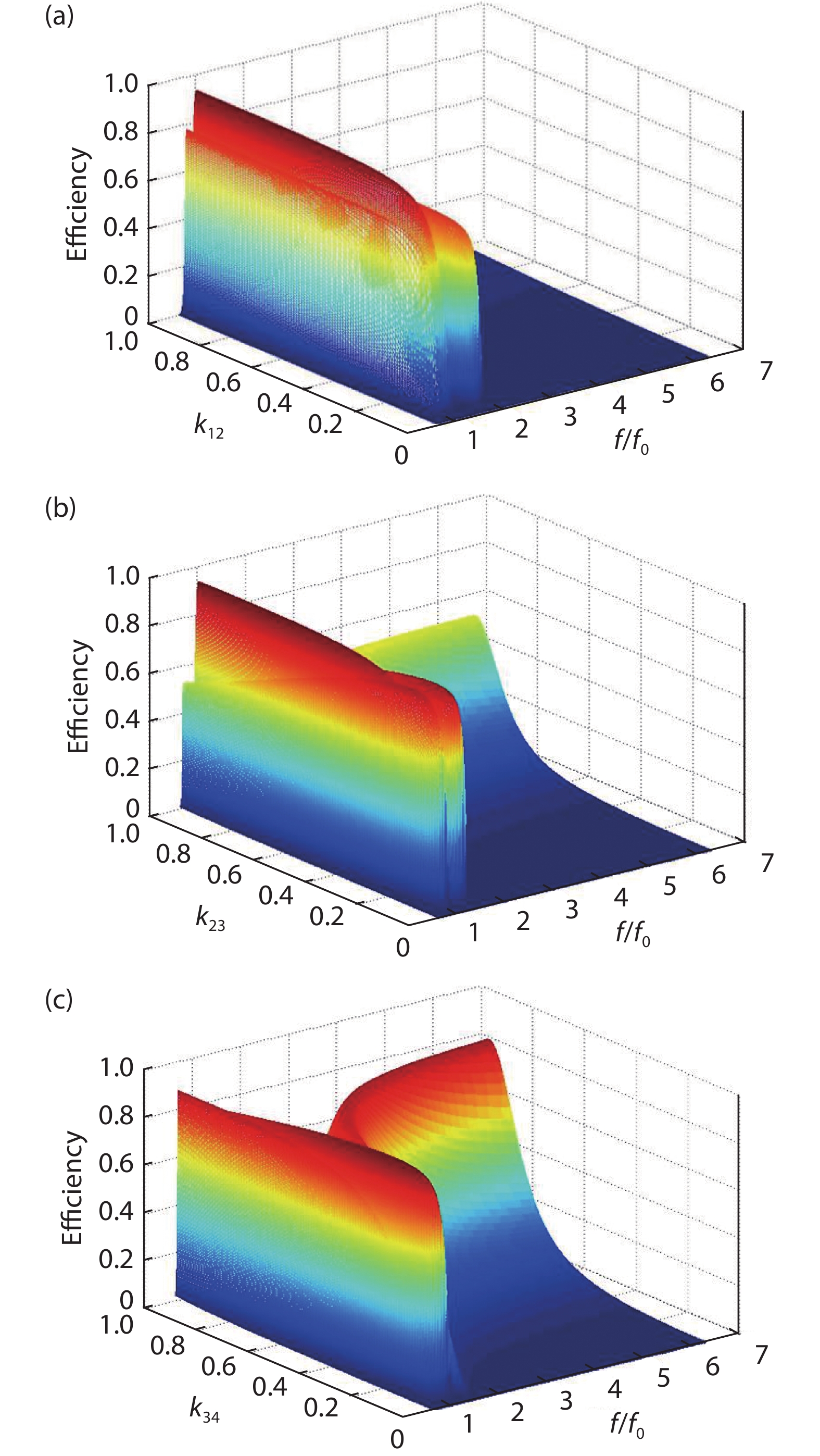
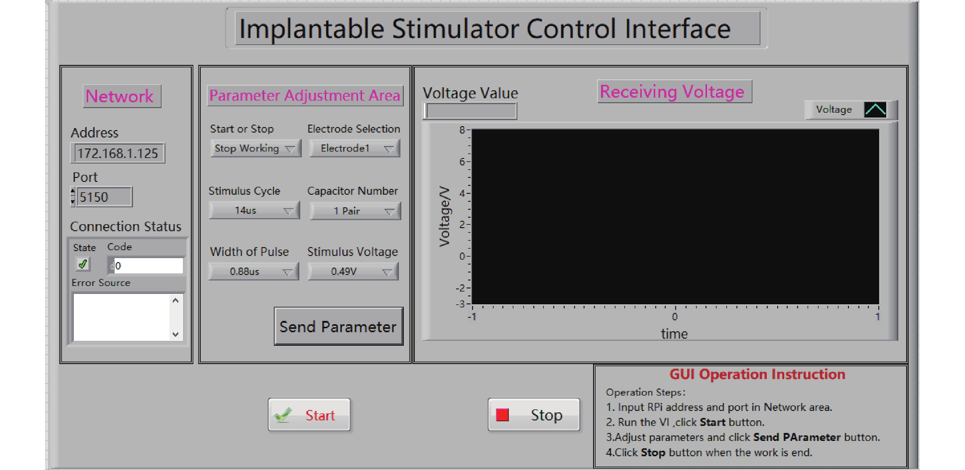
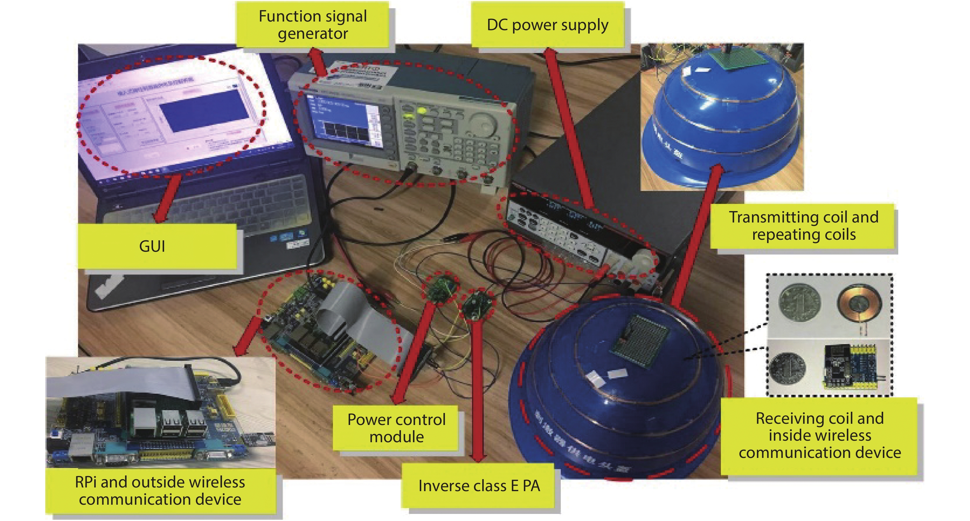
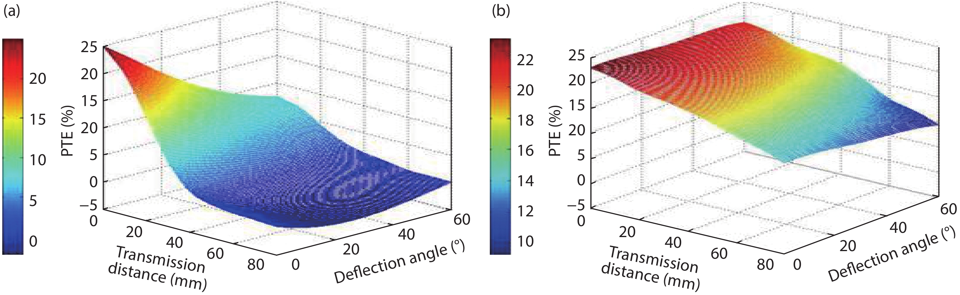
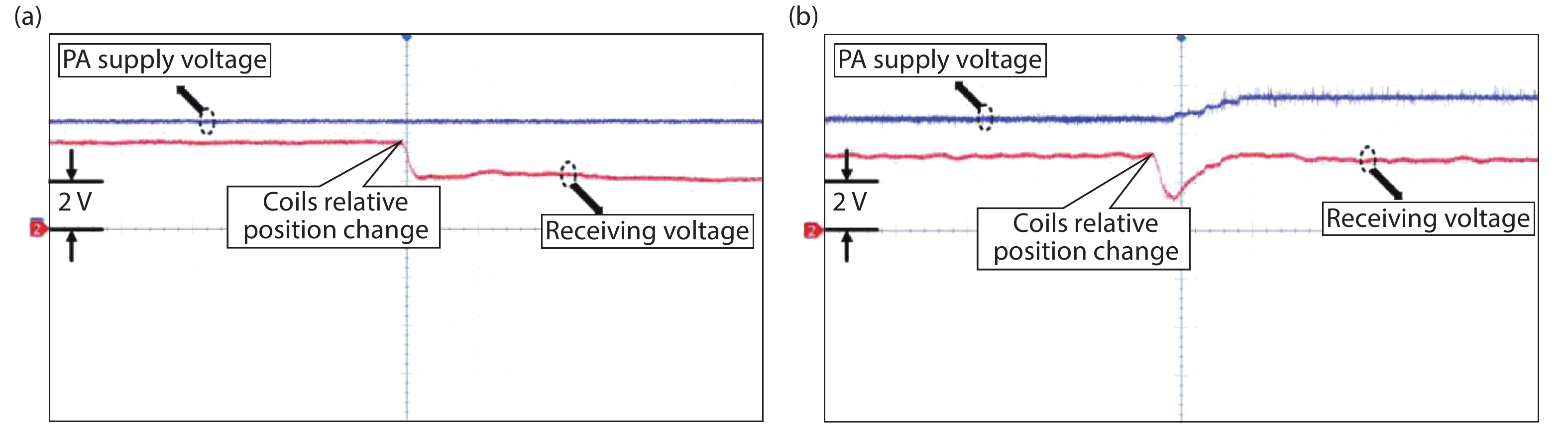
Traditional magnetically coupled resonant wireless power transfer technology uses fixed distances between coils for research, to prevent fluctuations in the receiving voltage, and lead to reduce transmission efficiency. This paper proposes a closed-loop control wireless communication wireless power transfer system with a wearable four-coil structure to stabilize the receiving voltage fluctuation caused by changes in the displacement between the coils. Test results show that the system can provide stable receiving voltage, no matter how the distance between the transmitting coil and the receiving coil is changed. When the transmission distance is 20 mm, the power transfer efficiency of the system can reach 18.5% under the open-loop state, and the stimulus parameters such as the stimulation period and pulse width can be adjusted in real time through the personal computer terminal.


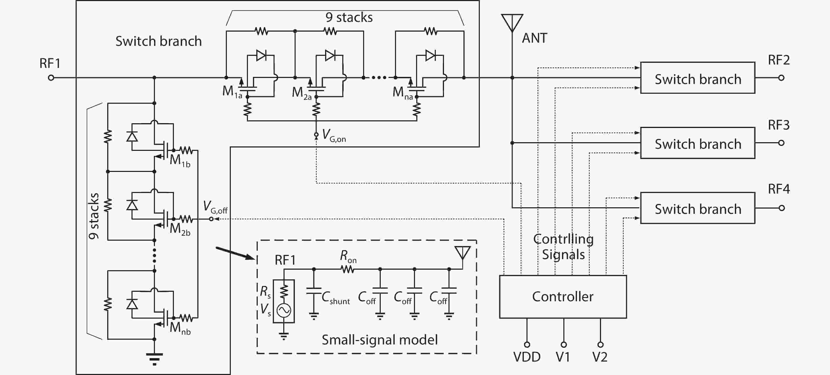
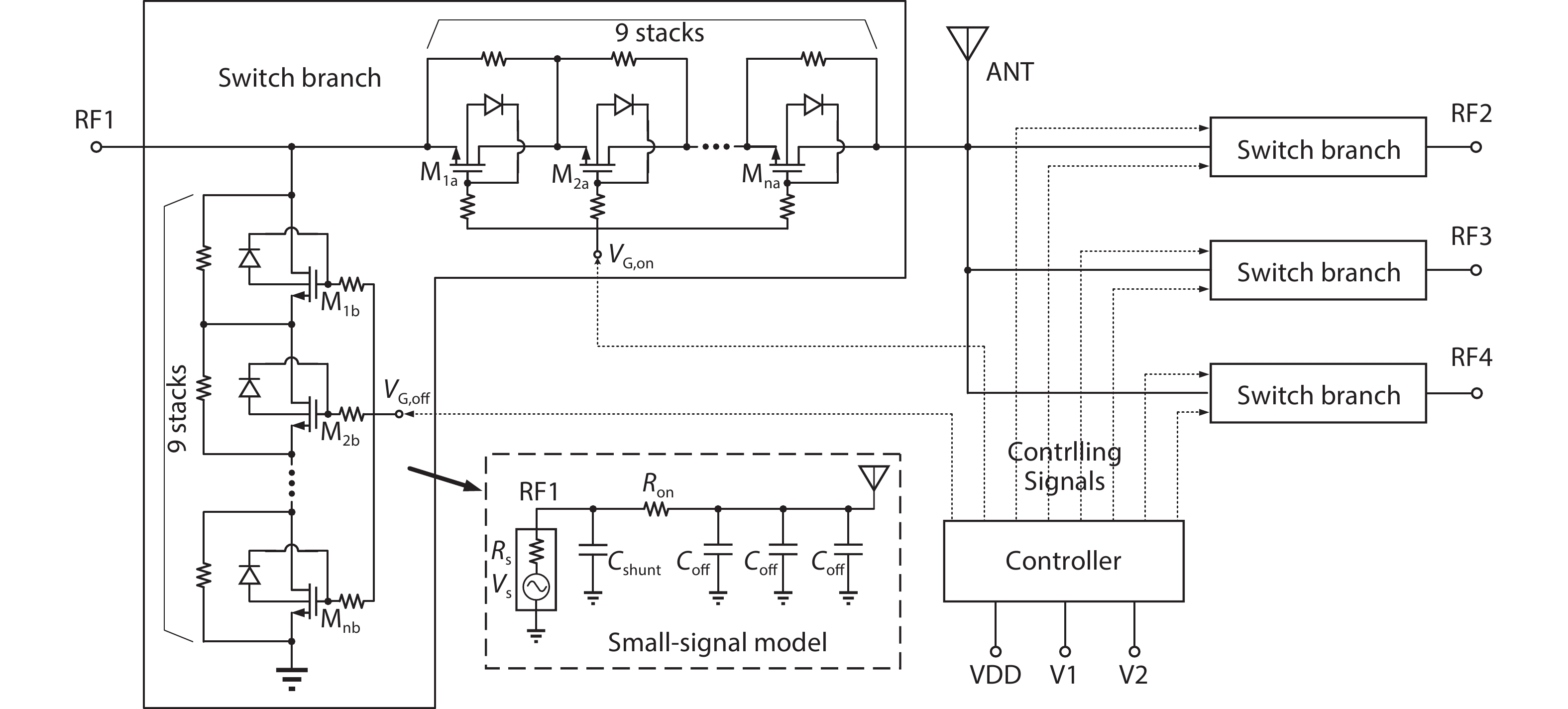
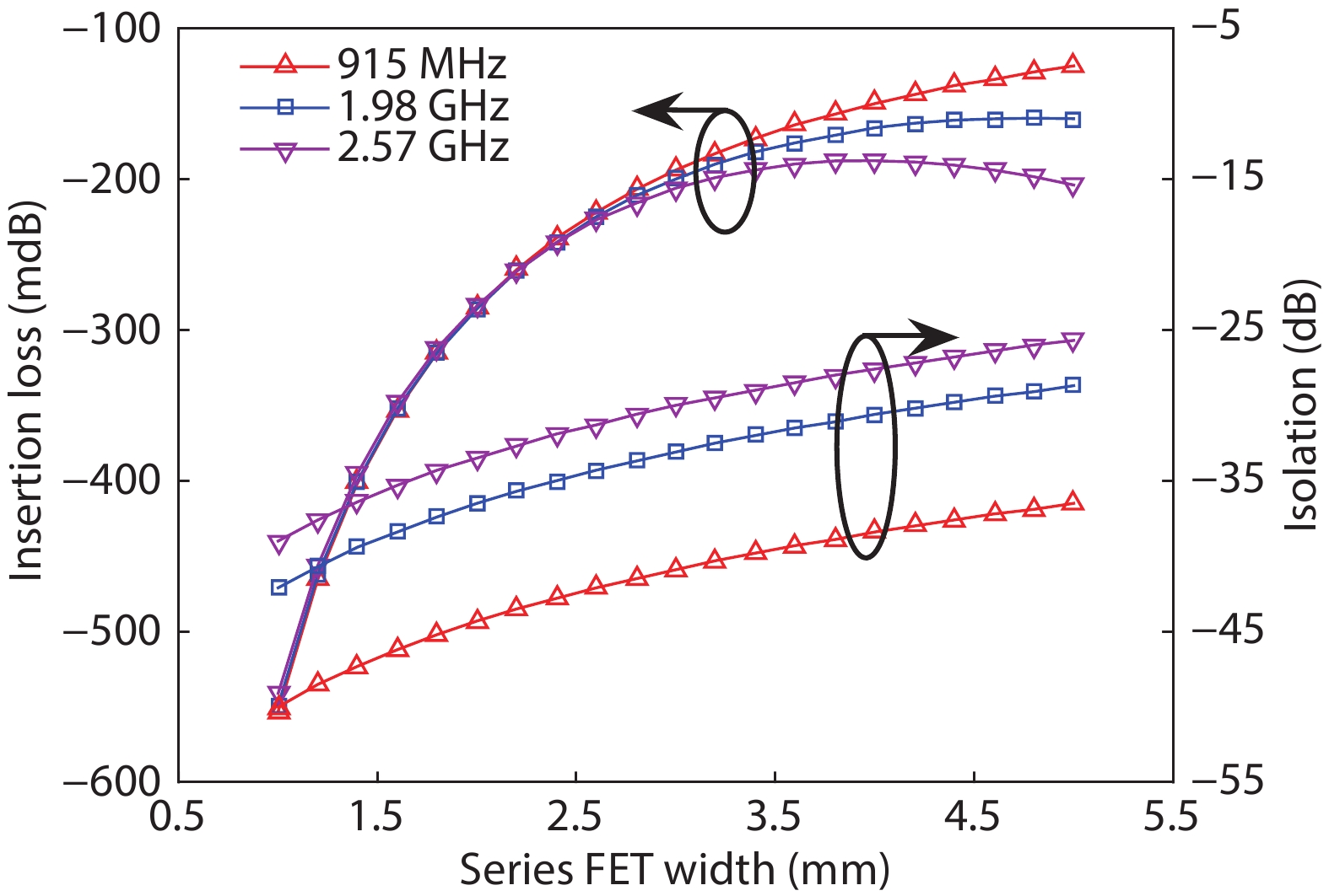
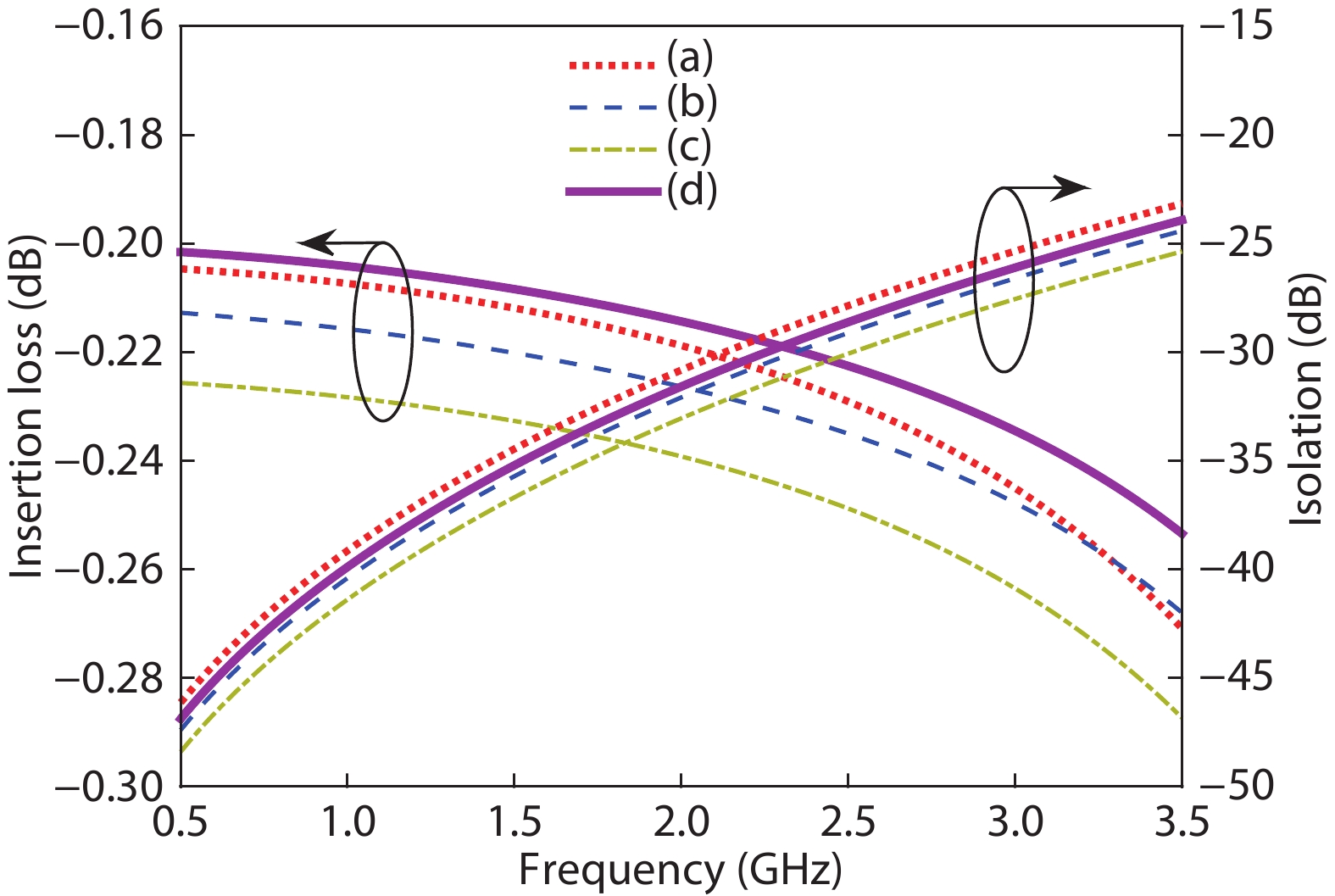
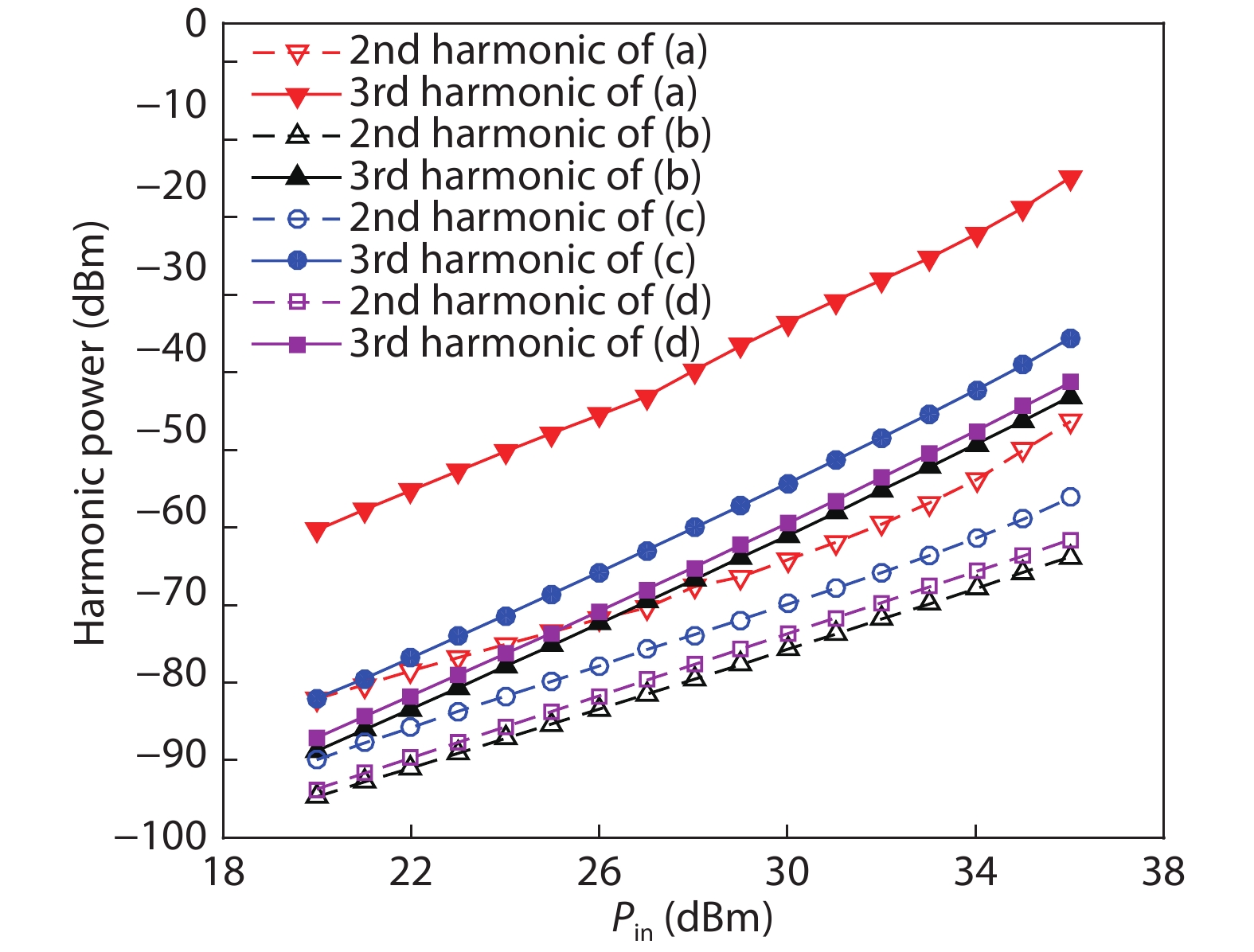
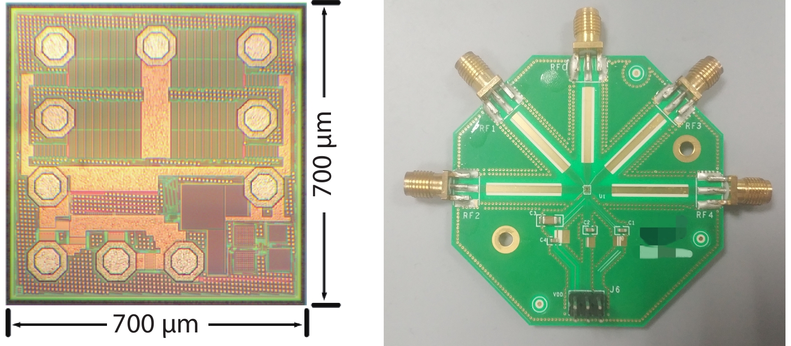
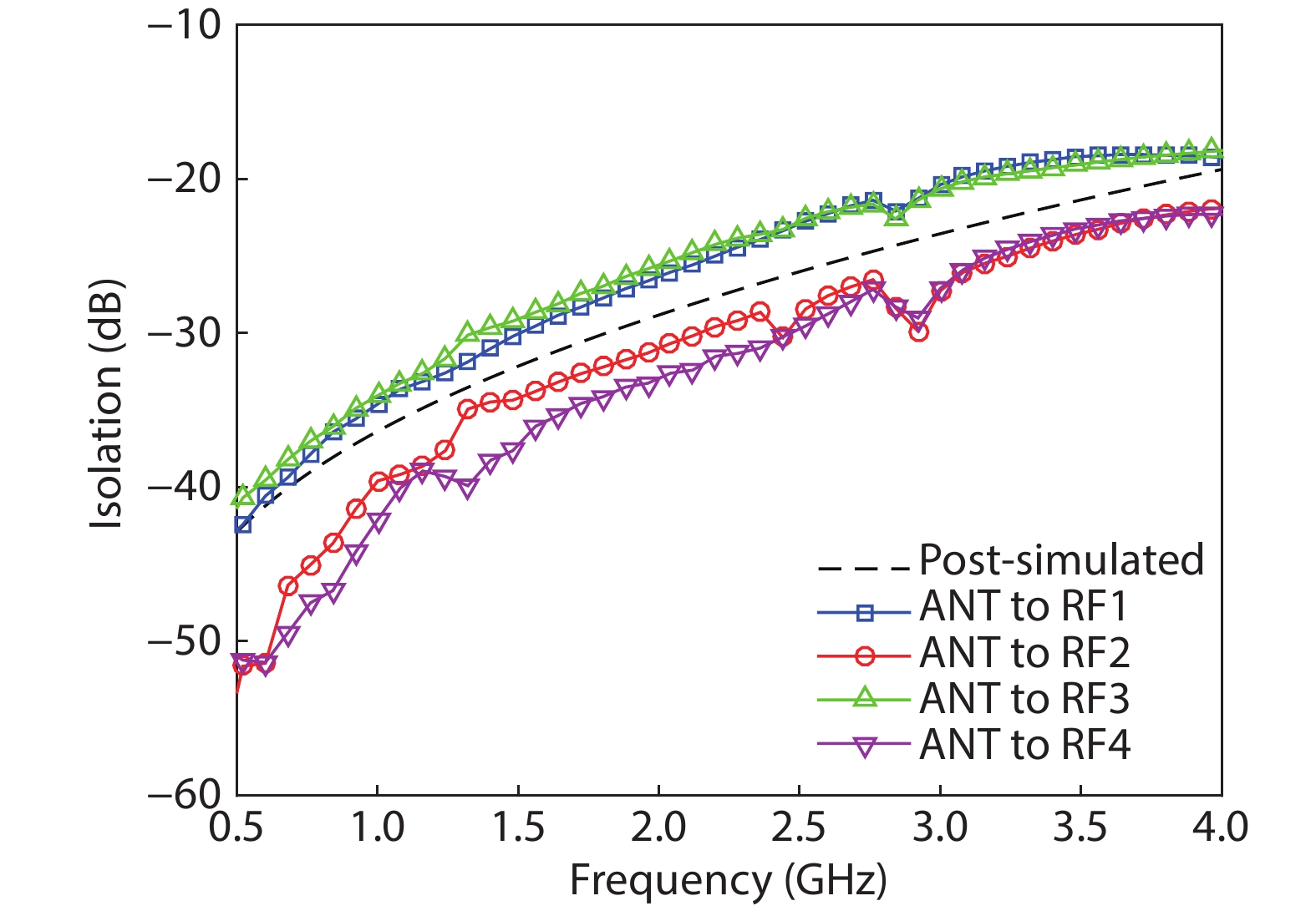
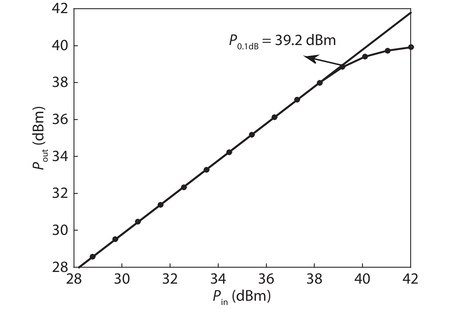
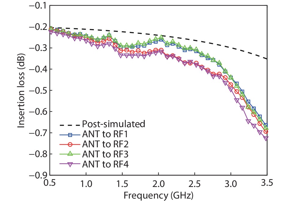
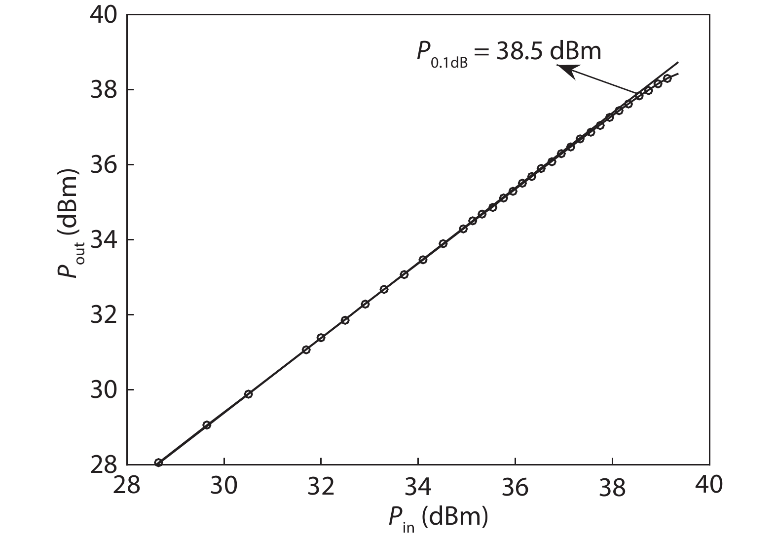
A single-pole four-throw (SP4T) RF switch with charge-pump-based controller is designed and implemented in a commercial 130-nm silicon-on-insulator (SOI) CMOS process. An improved body self-biasing technique based on diodes is utilized to simplify the controlling circuitry and improve the linearity. A multistack field-effect-transistor (FET) structure with body floating technique is employed to provide good power-handling capability. The proposed design demonstrates a measured input 0.1-dB compression point of 38.5 dBm at 1.9 GHz, an insertion loss of 0.27 dB/0.33 dB and an isolation of 35 dB/27 dB at 900 MHz/1.9 GHz, respectively. The overall chip area is only 0.49 mm2. This RF switch can be used in GSM/WCDMA/LTE front-end modules.


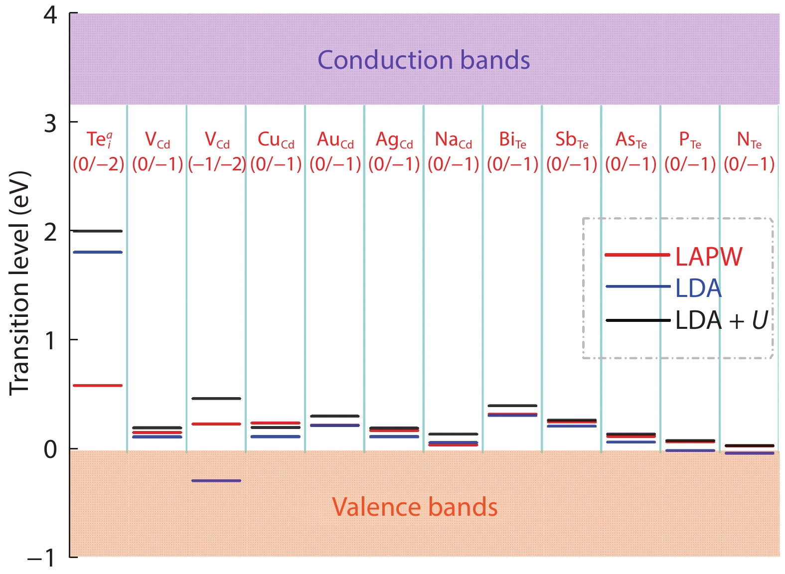
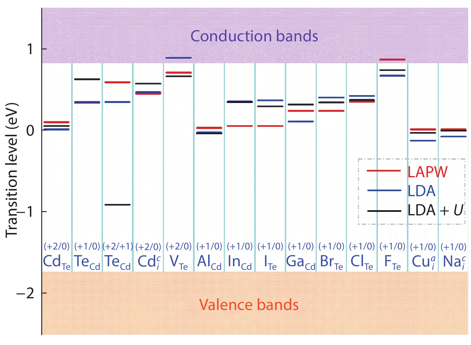
The defect properties in d-electron containing materials will be strongly influenced by the non-negligible on-site Coulomb interactions. However, this has been omitted in the current widely adopted standard first-principles calculations, such as LDA, leading to a large deviation of calculated results. Therefore, as a comparative case study, in this paper the defects of CdTe are investigated by first-principles calculations including standard LDA and LDA + U, and we find that LDA + U gives more accurate formation energies of the neutral point defects than the standard LDA. The same trend can be found in transition energies of the charged state defects as well. These comparative analyses show that LDA + U gives better results for the defects of CdTe than the standard LDA and requires less computing resource than LAPW, indicating it should have huge potential to model supercells with large number of atoms and strong electron interactions. Moreover, a new anion interstitial defect structure is found to be more stable than the well-known tetrahedron central anion interstitial defect structure


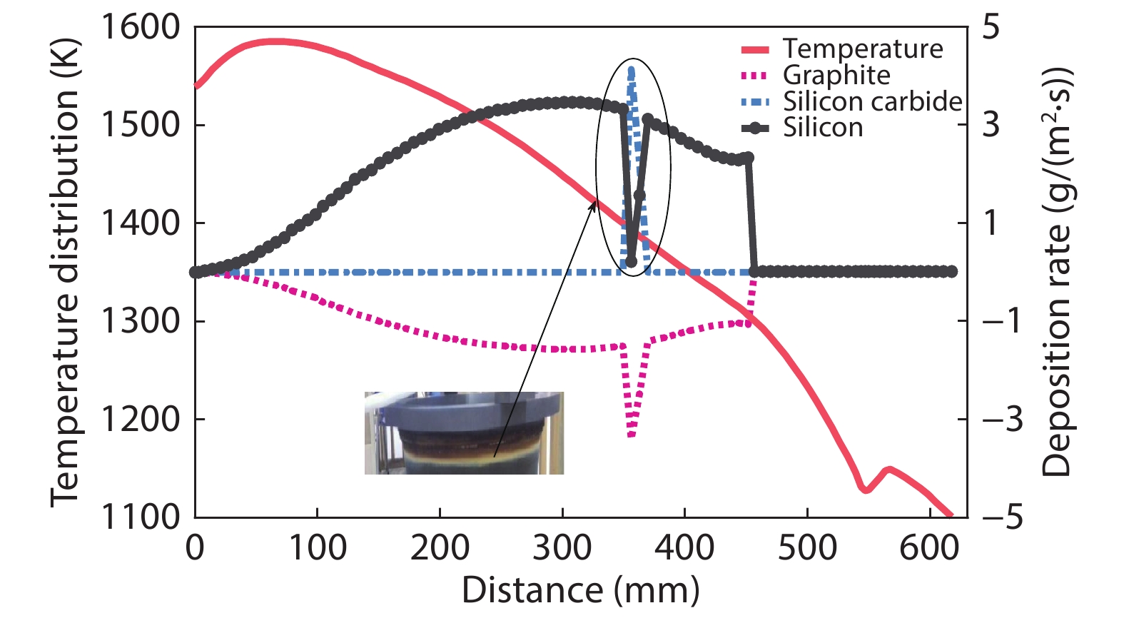
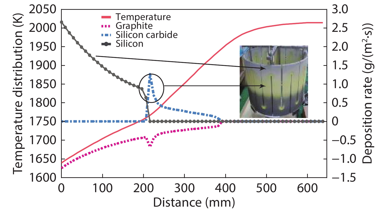
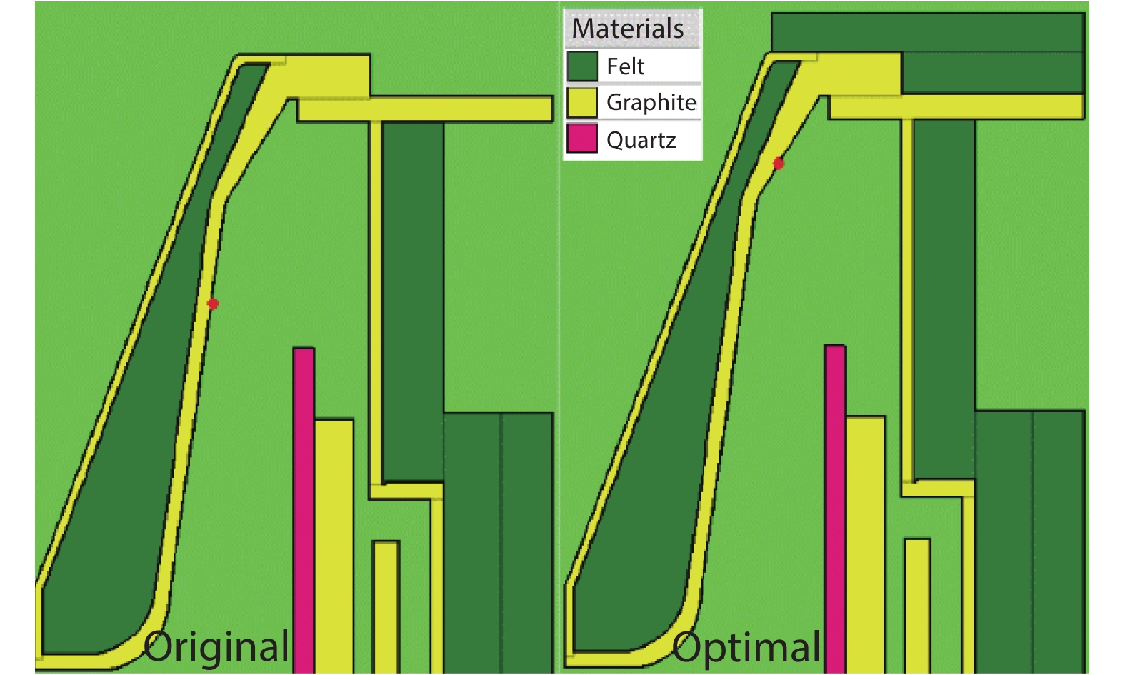
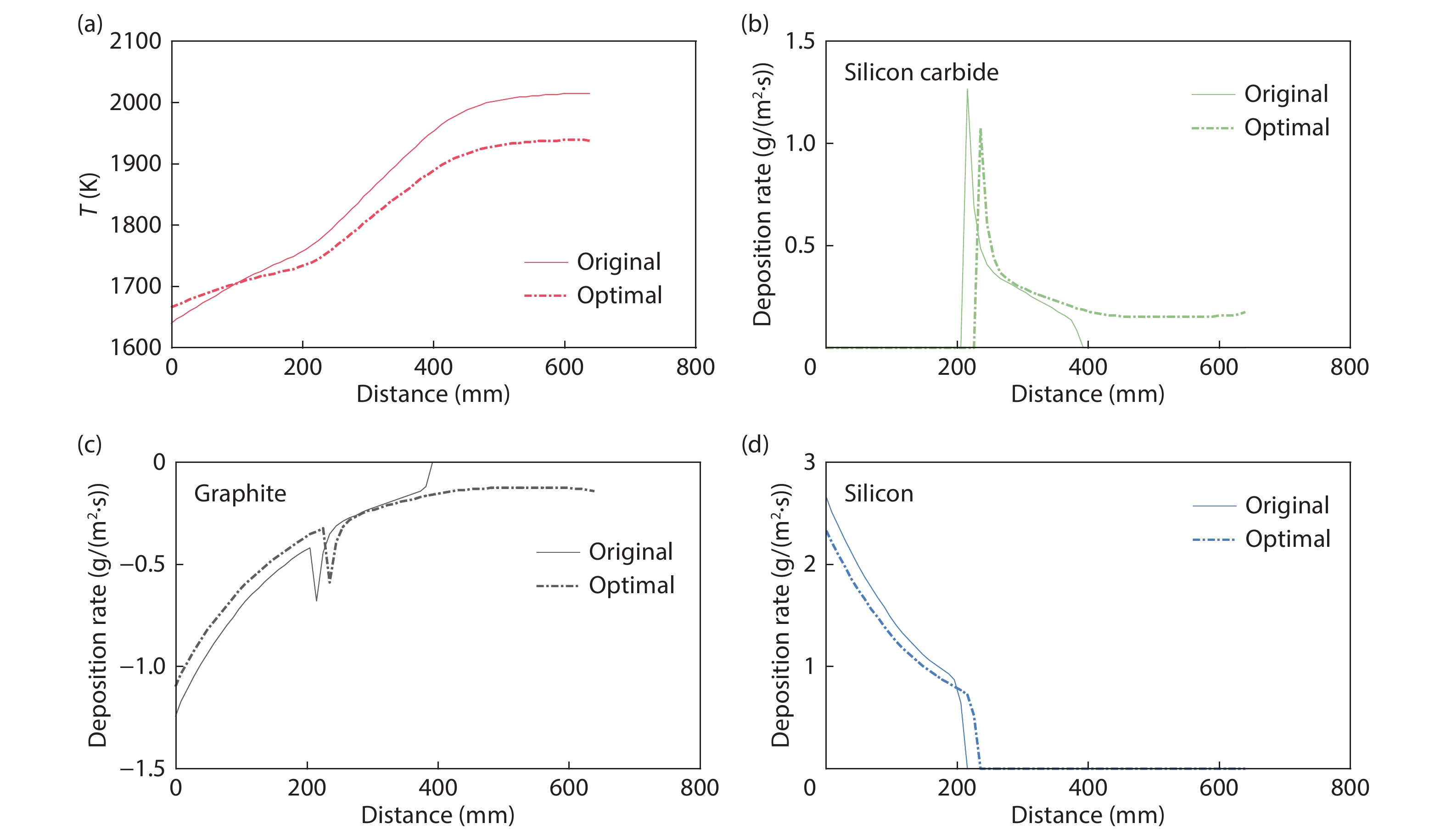
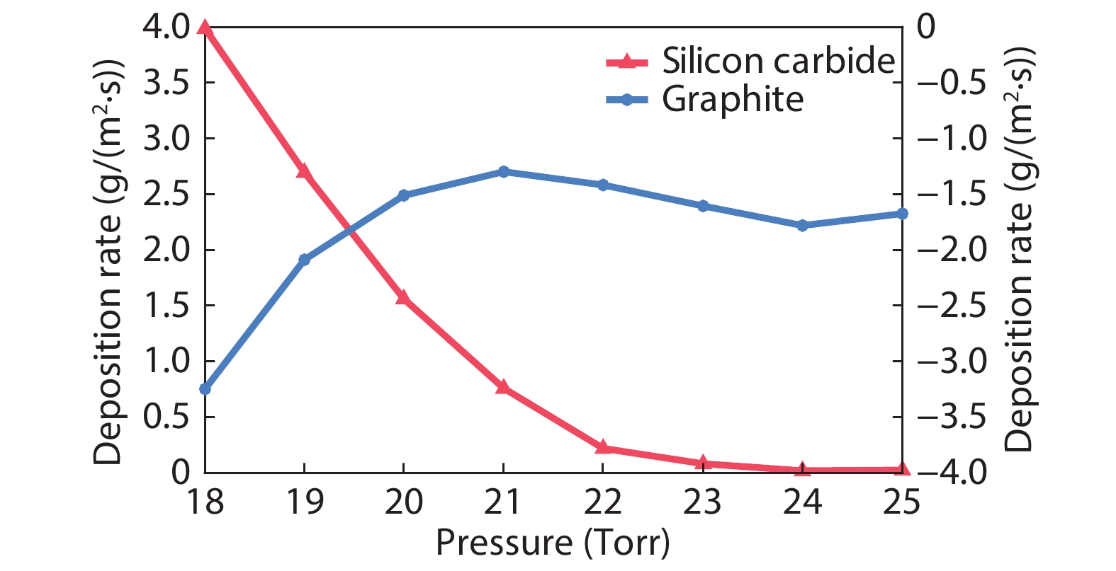
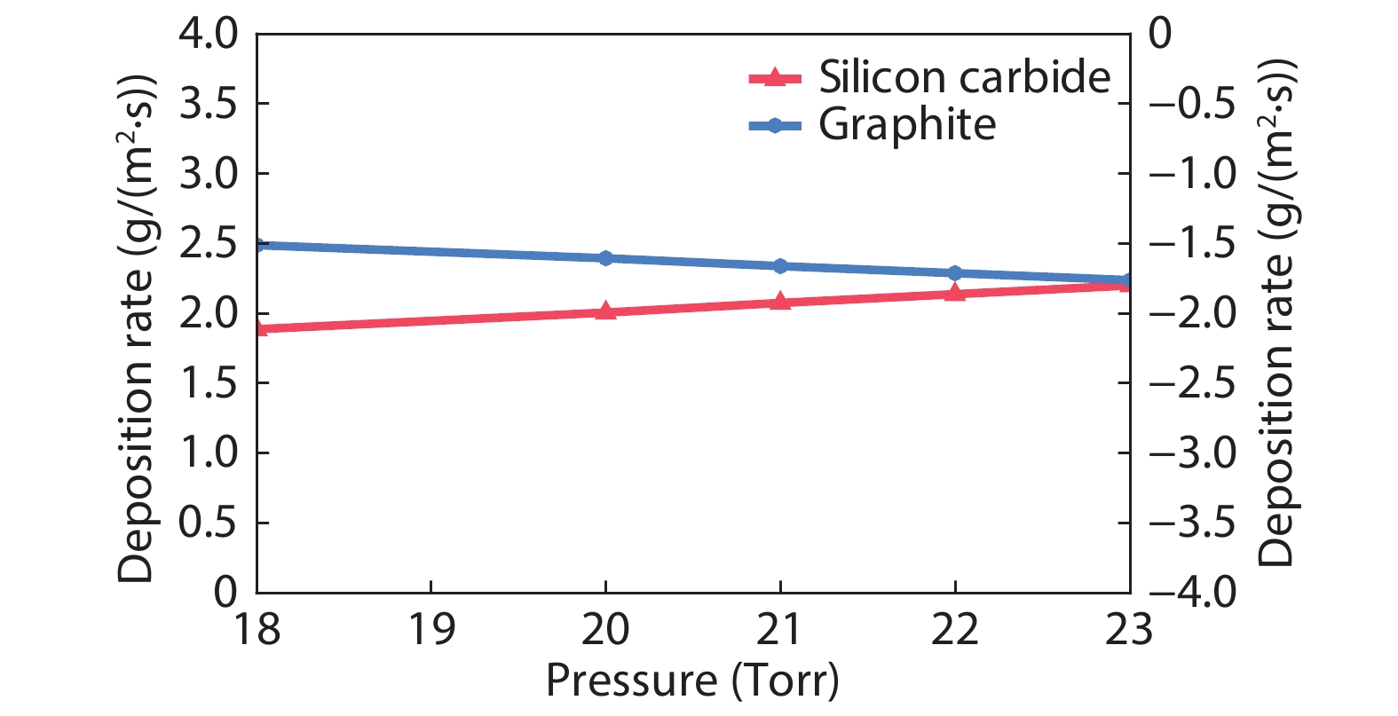
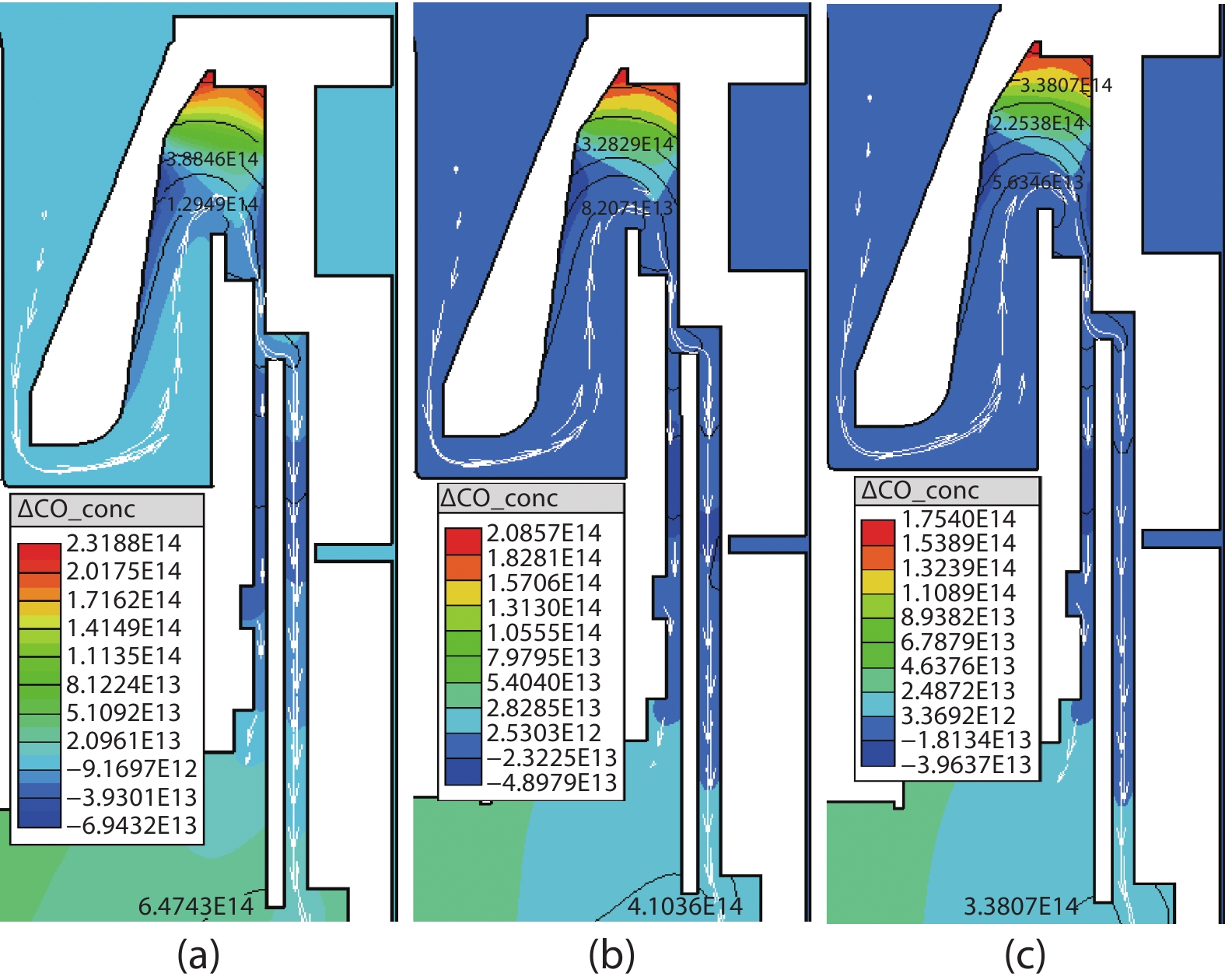
When preparing large monocrystalline silicon materials, severe carbon etching and silicide deposition often occur to the thermal system. Therefore, a suppression method that optimizes the upper insulation structure has been proposed. Assisted by the finite element method, we calculated temperature distribution and carbon deposition of heater and heat shield, made the rule of silicide and temperature distributing in the system, and we explained the formation of impurity deposition. Our results show that the optimized thermal system reduces carbon etching loss on heat components. The lowered pressure of the furnace brings a rapid decrease of silicide deposition. The increase of the argon flow rate effectively inhibits CO and back diffusion. The simulated results agree well with the experiment observations, validating the effectiveness of the proposed method.


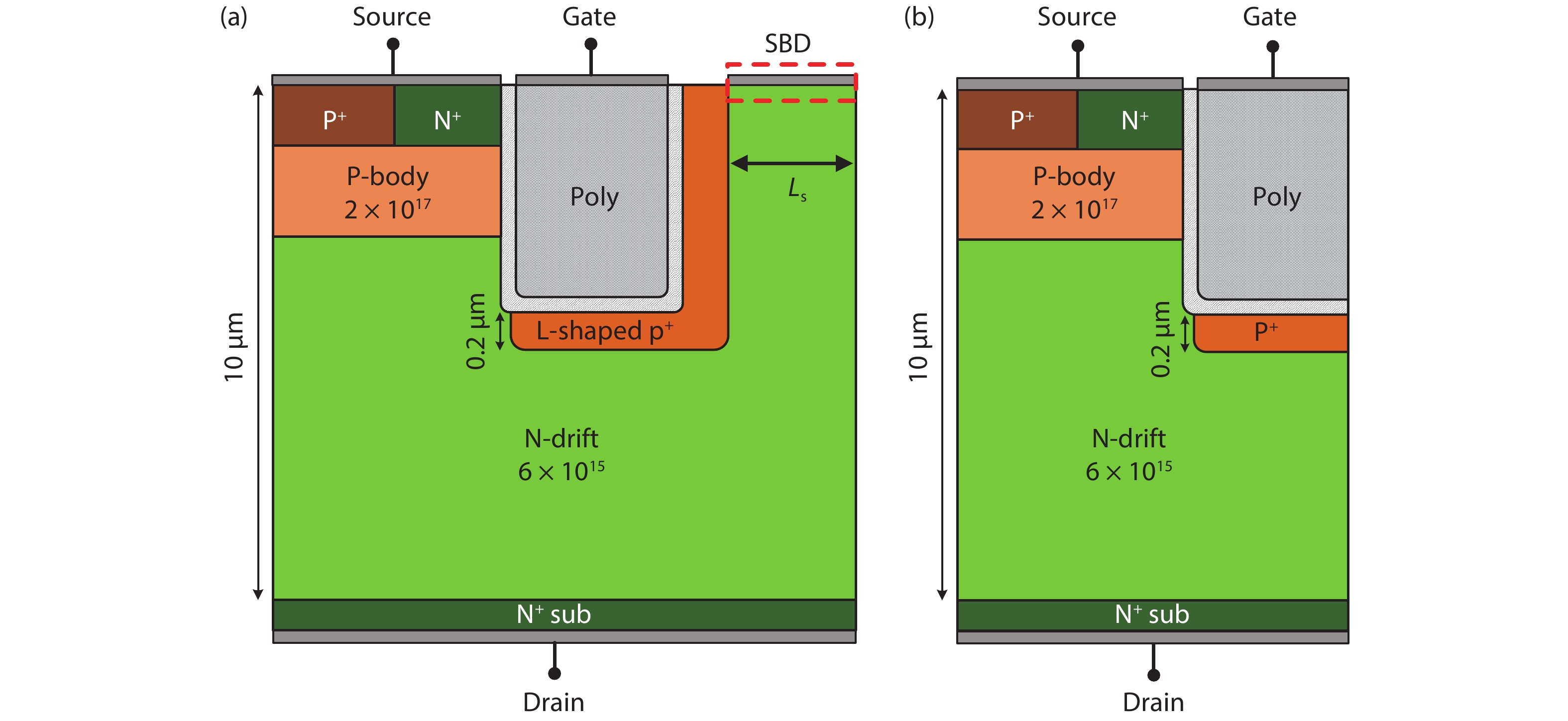
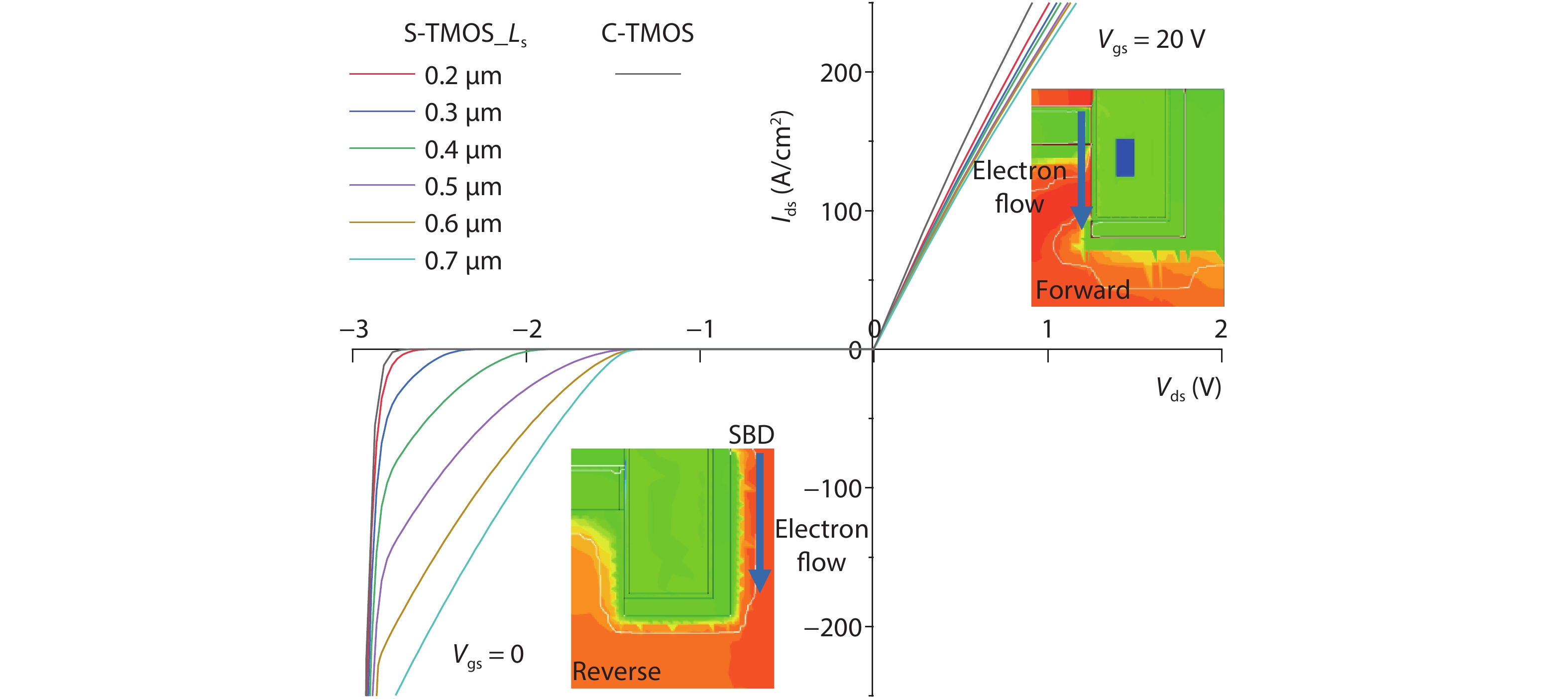
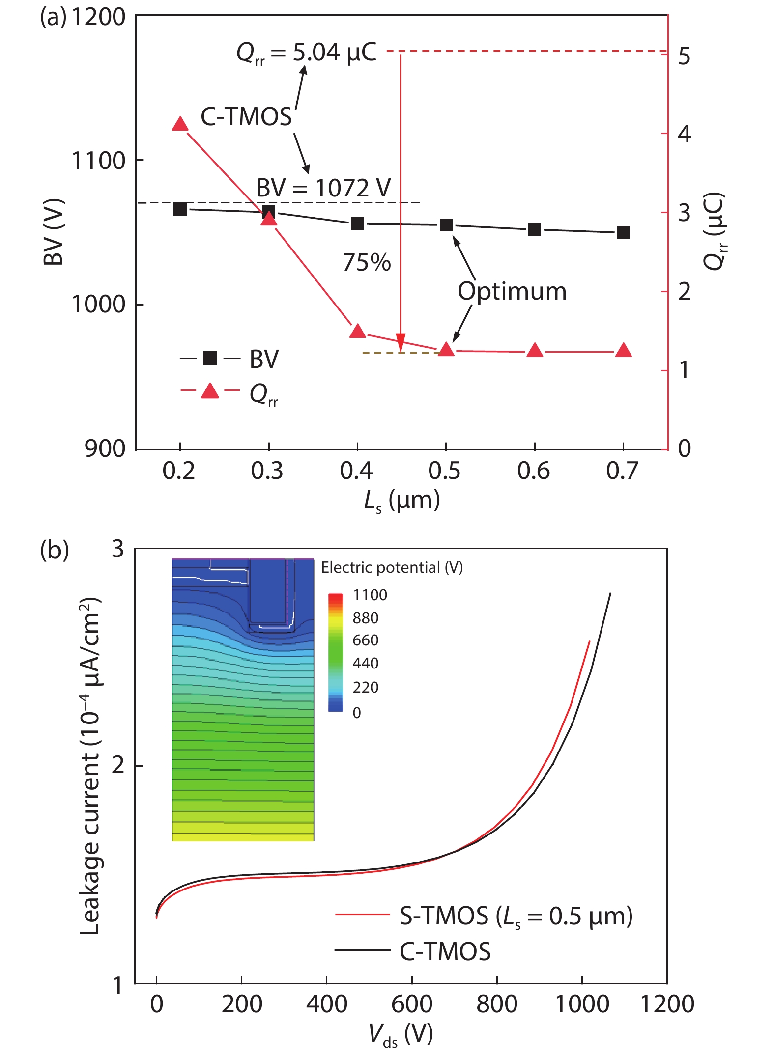
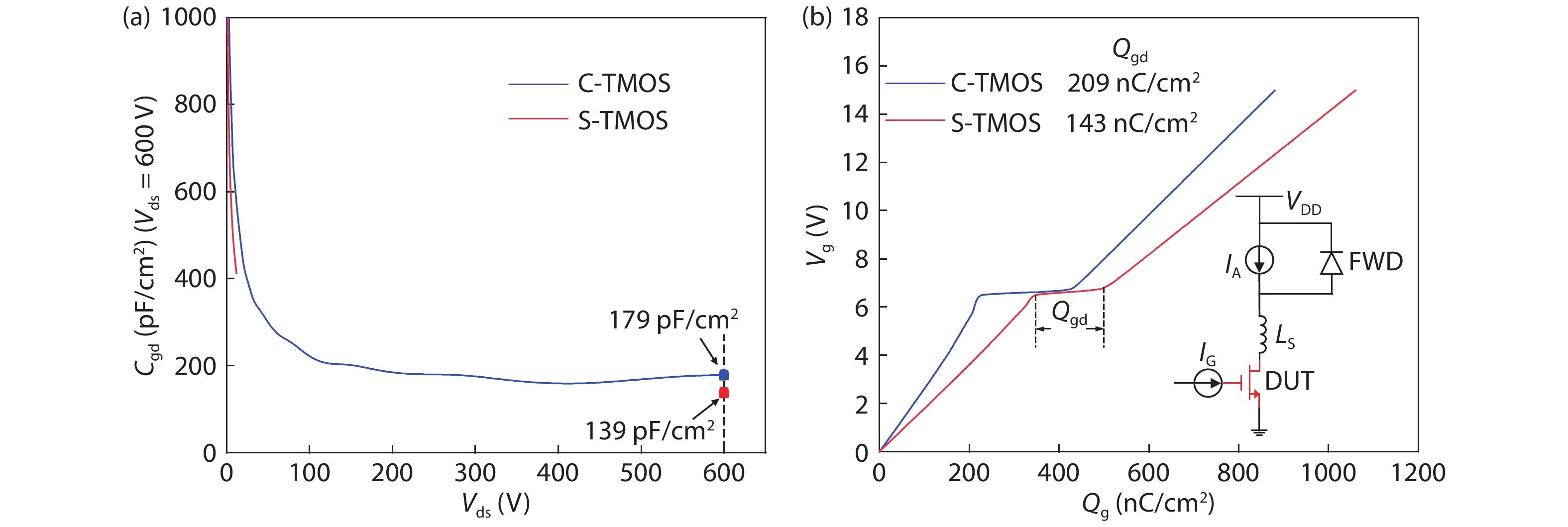
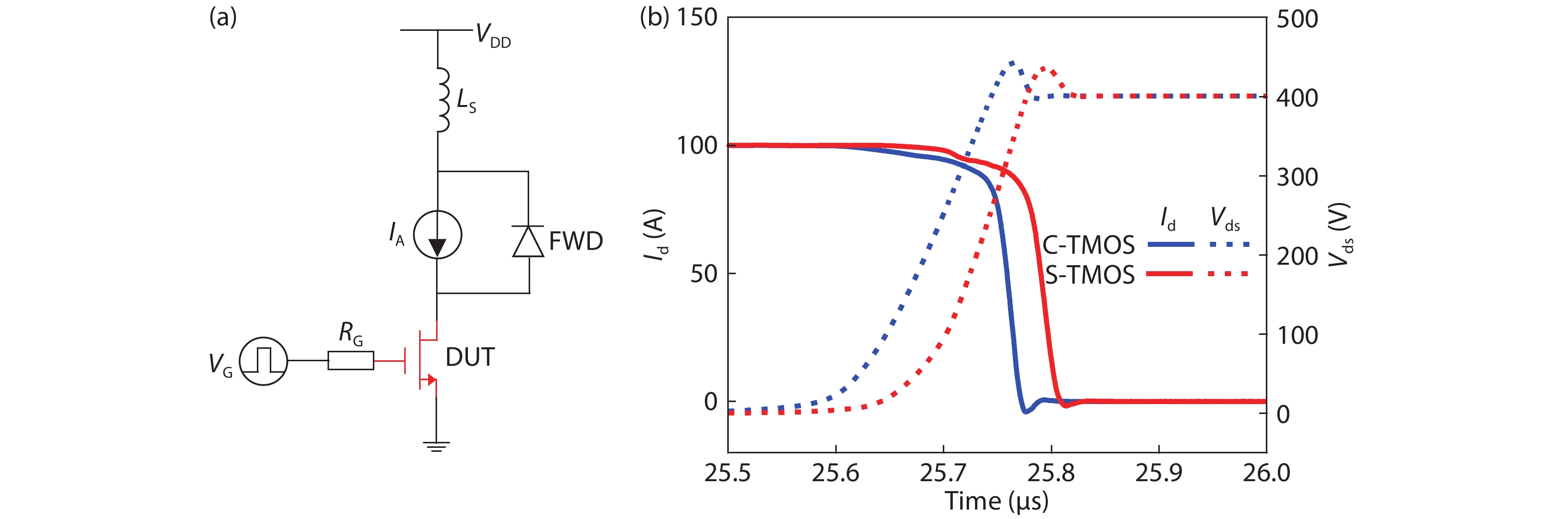
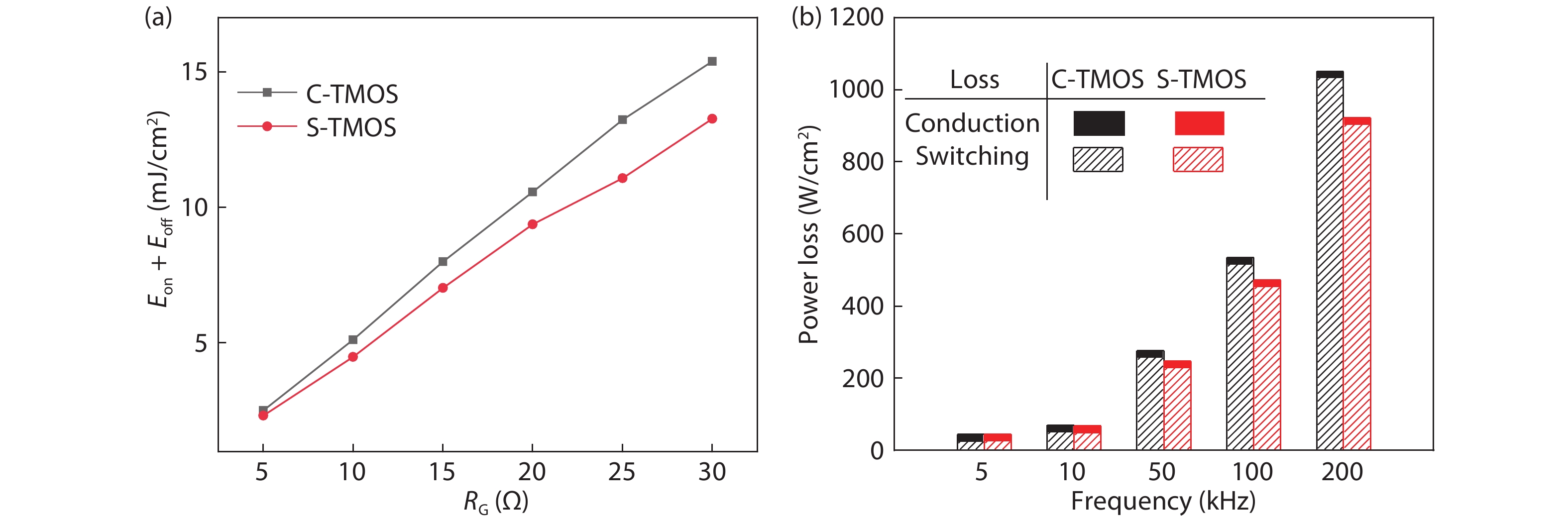
A novel 4H-SiC trench MOSFET is presented and investigated by simulation in this paper. The device features an integrated Schottky barrier diode and an L-shaped P+ shielding region beneath the gate trench and aside one wall of the gate trench (S-TMOS). The integrated Schottky barrier diode works as a free-wheeling diode in reverse recovery and reverse conduction, which significantly reduces reverse recovery charge (Qrr) and reverse turn-on voltage (VF). The L-shaped P+ region effectively shields the coupling of gate and drain, resulting in a lower gate–drain capacitance (Cgd) and date–drain charge (Qgd). Compared with that of conventional SiC trench MOSFET (C-TMOS), the VF and Qrr of S-TMOS has reduced by 44% and 75%, respectively, with almost the same forward output current and reverse breakdown voltage. Moreover, the S-TMOS reduces Qgd and Cgd by 32% and 22%, respectively, in comparison with C-TMOS.


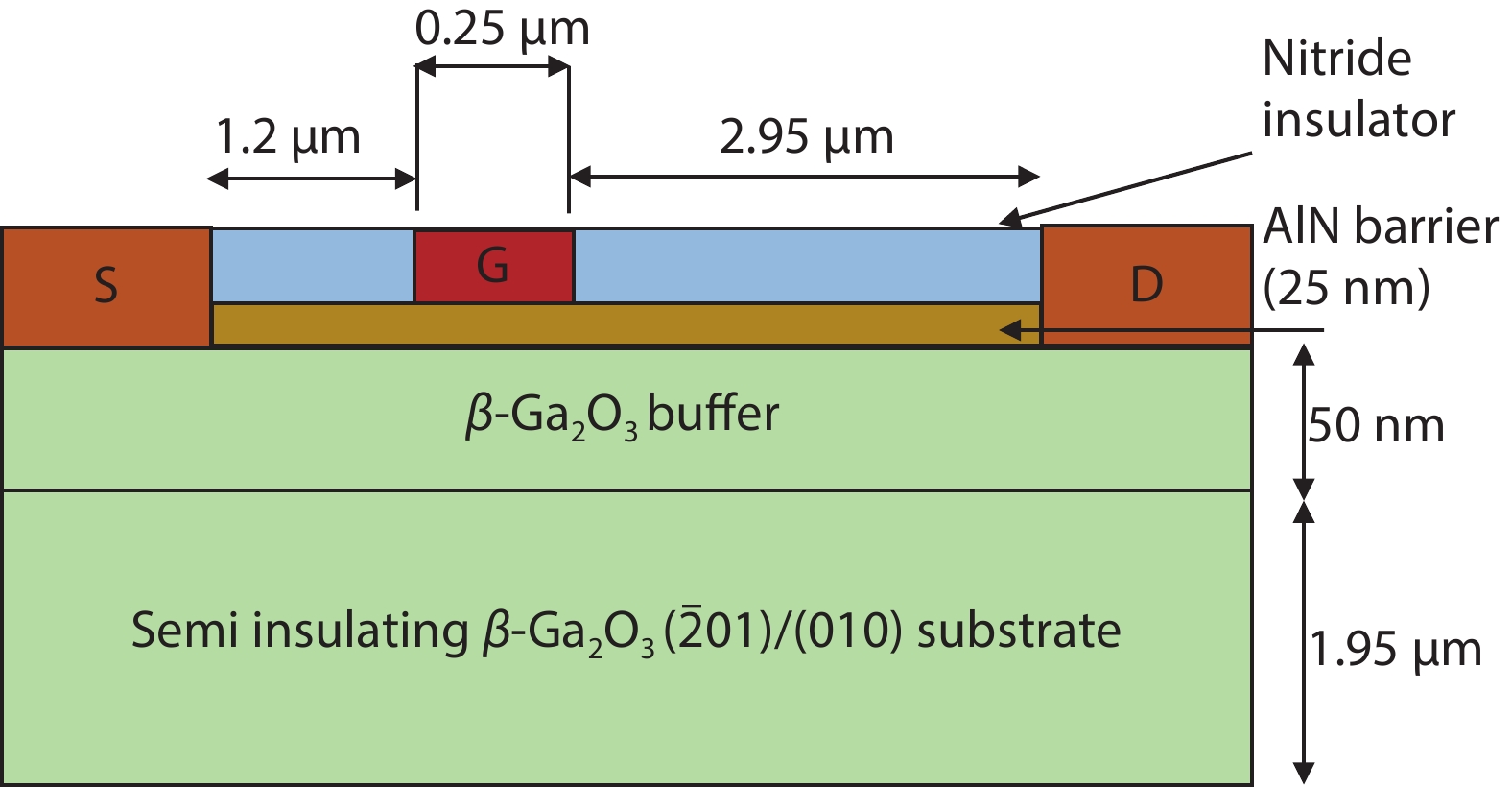
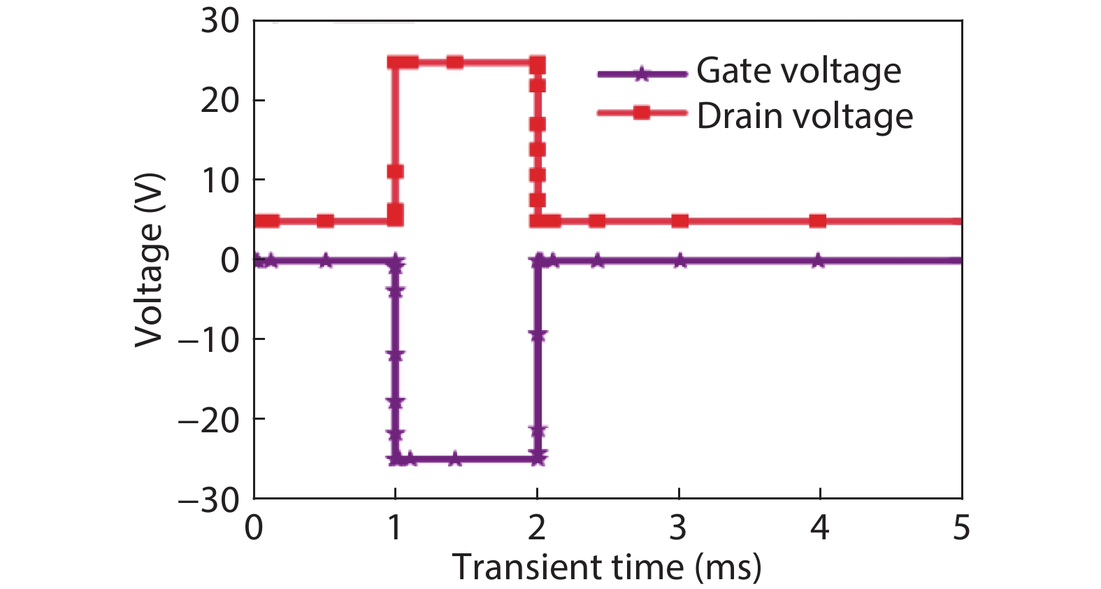
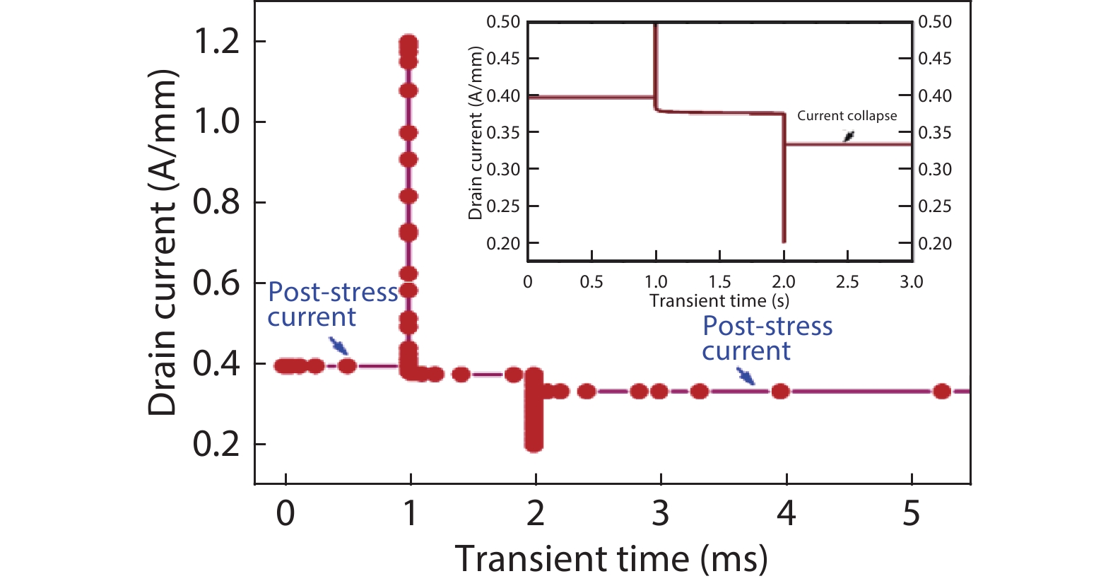
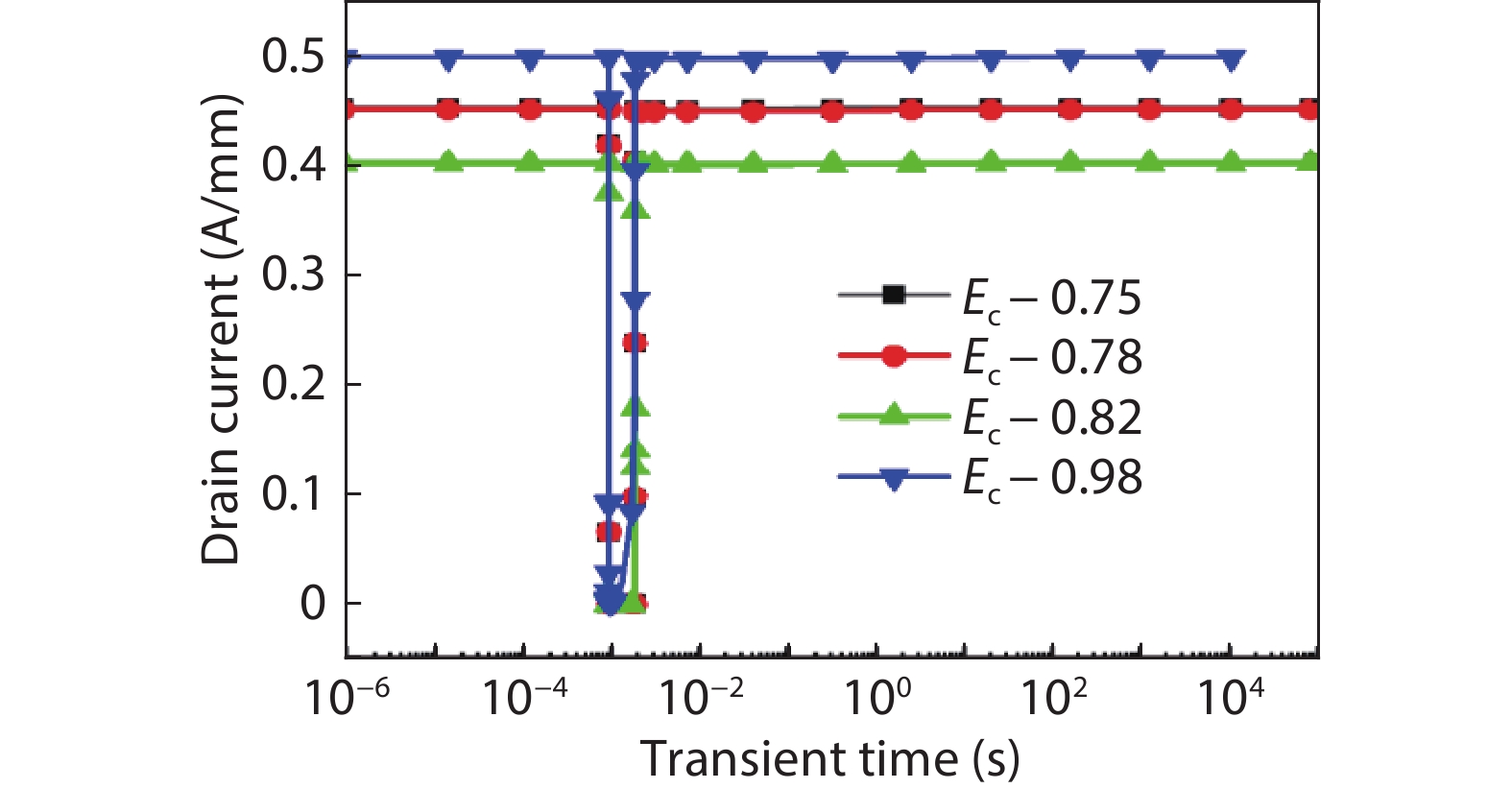
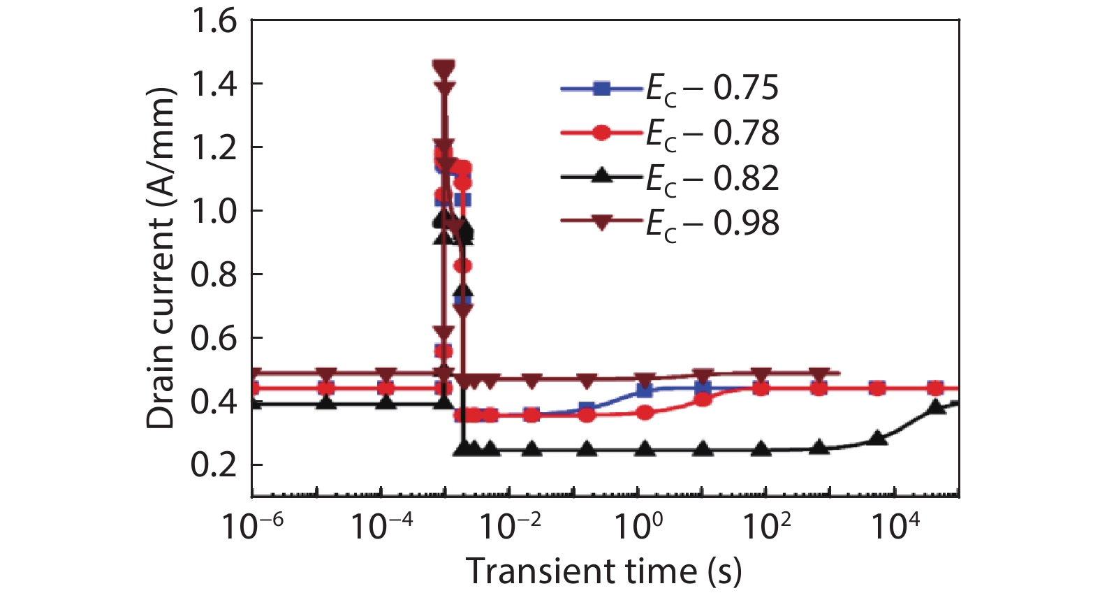
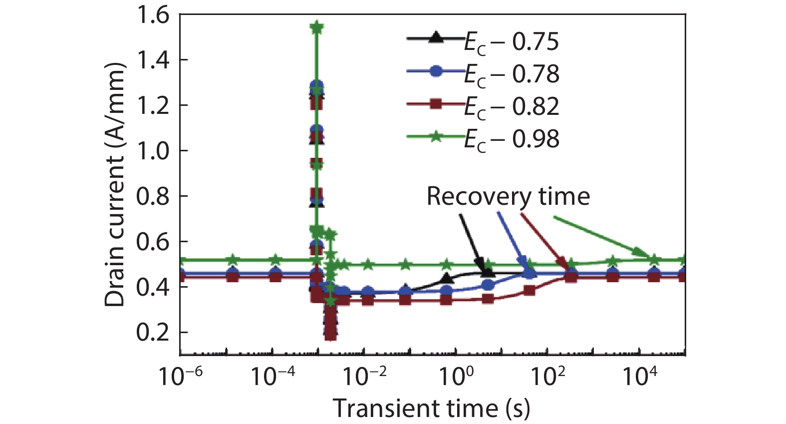
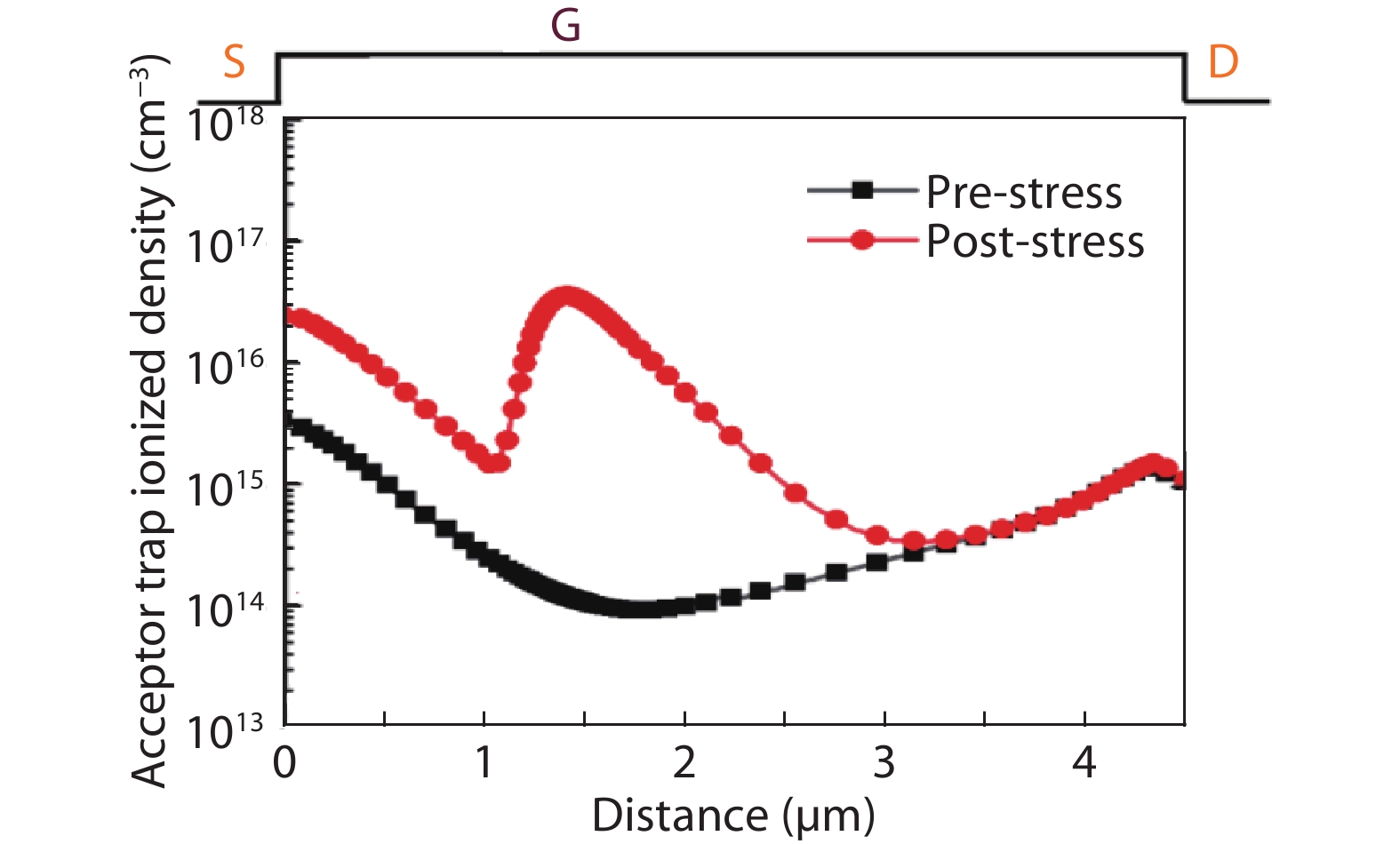
In this paper, drain current transient characteristics of β-Ga2O3 high electron mobility transistor (HEMT) are studied to access current collapse and recovery time due to dynamic population and de-population of deep level traps and interface traps. An approximately 10 min, and 1 h of recovery time to steady-state drain current value is measured under 1 ms of stress on the gate and drain electrodes due to iron (Fe)–doped β-Ga2O3 substrate and germanium (Ge)–doped β-Ga2O3 epitaxial layer respectively. On-state current lag is more severe due to widely reported defect trap EC – 0.82 eV over EC – 0.78 eV, −0.75 eV present in Iron (Fe)-doped β-Ga2O3 bulk crystals. A negligible amount of current degradation is observed in the latter case due to the trap level at EC – 0.98 eV. It is found that occupancy of ionized trap density varied mostly under the gate and gate–source area. This investigation of reversible current collapse phenomenon and assessment of recovery time in β-Ga2O3 HEMT is carried out through 2D device simulations using appropriate velocity and charge transport models. This work can further help in the proper characterization of β-Ga2O3 devices to understand temporary and permanent device degradation.