SEMICONDUCTOR DEVICES

Two dimensional analytical model for a negative capacitance double gate tunnel field effect transistor with ferroelectric gate dielectric

Huifang Xu

+ Author Affiliations

 Corresponding author: Huifang Xu, xu0342@163.com

PDF

Turn off MathJax

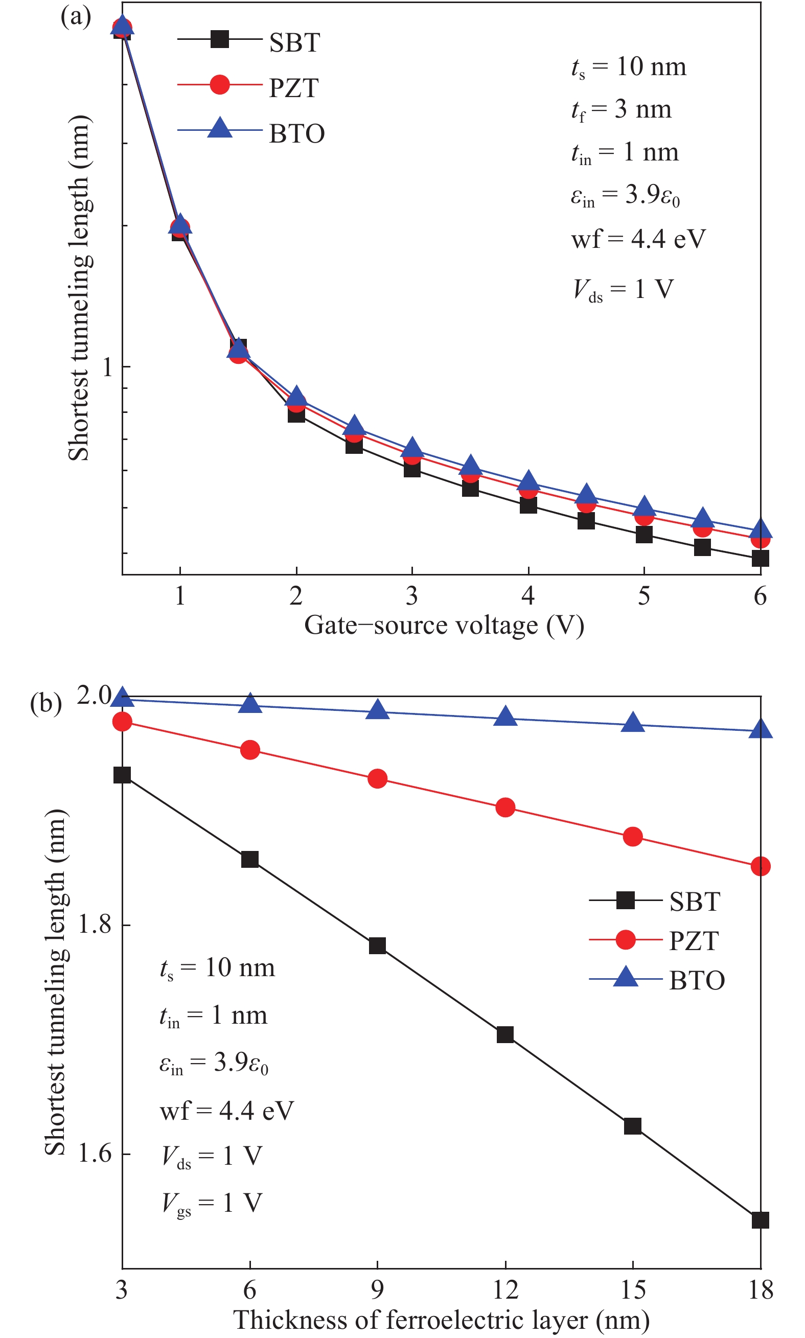
Abstract: Analytical models are presented for a negative capacitance double-gate tunnel field-effect transistor (NC DG TFET) with a ferroelectric gate dielectric in this paper. The model accurately calculates the channel potential profile by solving the Poisson equation with the Landau–Khalatnikov (LK) equation. Moreover, the effects of the channel mobile charges on the potential are also taken into account. We also analyze the dependences of the channel potential and the on-state current on the device parameters by changing the thickness of ferroelectric layer, ferroelectric material and also verify the simulation results accord with commercial TCAD. The results show that the device can obtain better characteristics when the thickness of the ferroelectric layer is larger as it can reduce the shortest tunneling length.

Key words: ferroelectric gate dielectricdouble-gate tunnel field-effect transistoranalytical model


[1]
Prabhat V, Dutta A K. Analytical surface potential and drain current models of dual-metal-gate double-gate tunnel-FETs. IEEE Trans Electron Devices, 2016, 63(5): 2190 doi: 10.1109/TED.2016.2541181
[2]
Mohammadi S, Khaveh H R T. An analytical model for double-gate tunnel FETs considering the junctions depletion regions and the channel mobile charge carriers. IEEE Trans Electron Devices, 2017, 64(3): 1268
[3]
Nupur N, Abhinav K. Overcoming the drawback of lower sense margin in tunnel FET based dynamic memory along with enhanced charge retention and scalability. Nanotechnology, 2017, 28: 445203 doi: 10.1088/1361-6528/aa8805
[4]
Kumar S, Goel E, Singh K, et al. A compact 2-D analytical model for electrical characteristics of double-gate tunnel field-effect transistors with a SiO2/high-k stacked gate-oxide structure. IEEE Trans Electron Devices, 2016, 63(8): 3291 doi: 10.1109/TED.2016.2572610
[5]
Navjeet B, Subir K S. An analytical model for tunnel barrier modulation in triple metal double gate TFET. IEEE Trans Electron Devices, 2015, 62(7): 2136 doi: 10.1109/TED.2015.2434276
[6]
Hraziia, Vladimirescu A, Amara A, et al. An analysis on the ambipolar current in Si double-gate tunnel FETs. Solid-State Electron, 2012, 70(4): 67
[7]
Wu J Z, Taur Y. Reduction of TFET OFF-current and subthreshold swing by lightly doped drain. IEEE Trans Electron Devices, 2016, 63(8): 3342 doi: 10.1109/TED.2016.2577589
[8]
Nigam K, Pandey S, Kondekar P N, et al. A barrier controlled charge plasma-based tfet with gate engineering for ambipolar suppression and RF/linearity performance improvement. IEEE Trans Electron Devices, 2017, 64(6): 2751 doi: 10.1109/TED.2017.2693679
[9]
Raad B R, Sharma D, Kondekar P, et al. Drain work function engineered doping-less charge plasma TFET for ambipolar suppression and RF performance improvement: A proposal, design, and investigation. IEEE Trans Electron Devices, 2016, 63(10): 3950 doi: 10.1109/TED.2016.2600621
[10]
Ko E, Lee H, Park J D, et al. Vertical tunnel FET: design optimization with triple metal-gate layers. IEEE Trans Electron Devices, 2016, 63(12): 5030 doi: 10.1109/TED.2016.2619372
[11]
Boucart K, Ionescu A M. Double-gate tunnel FET with high-k gate dielectric. IEEE Trans Electron Devices, 2007, 54(7): 1725 doi: 10.1109/TED.2007.899389
[12]
Kao K H, Verhulst A S, Vandenberghe W G, et al. Direct and indirect band-to-band tunneling in germanium-based TFETs. IEEE Trans Electron Devices, 2012, 59(2): 292 doi: 10.1109/TED.2011.2175228
[13]
Ahish S, Sharma D, Kumar Y B N, et al. Performance enhancement of novel InAs/Si hetero double-gate tunnel FET using gaussian doping. IEEE Trans Electron Devices, 2016, 63(1): 288 doi: 10.1109/TED.2015.2503141
[14]
Yadav D S, Sharma D, Kumar A, et al. Performance investigation of hetero material (InAs/Si)-based charge plasma TFET. Micro Nano Lett, 2017, 12(6): 358 doi: 10.1049/mnl.2016.0688
[15]
Bagga N, Dasgupta S. Surface potential and drain current analytical model of gate all around triple metal TFET. IEEE Trans Electron Devices, 2017, 64(2): 606 doi: 10.1109/TED.2016.2642165
[16]
Abdi D B, Kumar M J. 2-D Threshold voltage model for the double-gate p–n–p–n TFET with localized charges. IEEE Trans Electron Devices, 2016, 63(9): 3663 doi: 10.1109/TED.2016.2589927
[17]
Wang Y B, Han G Q, Liu Y, et al. Investigation of GaAsBi/GaAsN type-II staggered heterojunction TFETs with the analytical model. IEEE Trans Electron Devices, 2017, 64(4): 1541 doi: 10.1109/TED.2017.2668063
[18]
Xu H F, Guan B G. Two-dimensional analytical model for hetero-junction double-gate tunnel field-effect transistor with a stacked gate-oxide structure. Jpn J Appl Phys, 2017, 56(5): 054201 doi: 10.7567/JJAP.56.054201
[19]
Zhao Y, Wu C L, Huang Q Q, et al. A novel tunnel FET design through adaptive bandgap engineering with constant sub-threshold slope over 5 decades of current and high ION/IOFF ratio. IEEE Electron Device Lett, 2017, 38(5): 540 doi: 10.1109/LED.2017.2679031
[20]
Kondekar P N, Nigam K, Pandey S, et al. Design and analysis of polarity controlled electrically doped tunnel FET with bandgap engineering for analog/RF applications. IEEE Trans Electron Devices, 2017, 64(2): 412 doi: 10.1109/TED.2016.2637638
[21]
Lahgere A, Panchore M, Singh J. Dopingless ferroelectric tunnel FET architecture for the improvement of performance of dopingless n-channel tunnel FETs. Superlattices Microstruct, 2016, 96: 16 doi: 10.1016/j.spmi.2016.05.004
[22]
Kale S, Kondekar P N. Ferroelectric Schottky barrier tunnel FET with gate-drain underlap: Proposal and investigation. Superlattices Microstruct., 2016, 89: 225.
[23]
Lee M H, Wei Y T, Lin J C, et al. Ferroelectric gate tunnel field-effect transistors with low-power steep turn-on. AIP Adv, 2014, 4(10): 107117 doi: 10.1063/1.4898150
[24]
Kobayashi M, Jang K, Ueyama N, et al. Negative capacitance for boosting tunnel FET performance. IEEE Trans Nanotechnol, 2017, 16(2): 253 doi: 10.1109/TNANO.2017.2658688
[25]
Liu C, Chen P G, Xie M J, et al. Simulation-based study of negative-capacitance double-gate tunnel field-effect transistor with ferroelectric gate stack. Jpn J Appl Phys, 2016, 55(4S): 04EB08 doi: 10.7567/JJAP.55.04EB08
[26]
Saeidi A, Biswas A, Ionescu A M. Modeling and simulation of low power ferroelectric non-volatile memory tunnel field effect transistors using silicon-doped hafnium oxide as gate dielectric. Solid-State Electron, 2016, 124(10): 16
[27]
Chowdhury N, Azad S M F, Khosru Q D M. Negative capacitance tunnel field effect transistor: A novel device with low subthreshold swing and high on current. ECS Trans, 2014, 58(16): 1 doi: 10.1149/05816.0001ecst
[28]
Chowdhury N, Ahmed I, Fakhrul T, et al. A low subthreshold swing tunneling field effect transistor for next generation low power CMOS applications. Physica E, 2015, 74(11): 251
[29]
Jiang C S, Liang R R, Xu J. Investigation of negative capacitance gate-all-around tunnel FETs combining numerical simulation and analytical modeling. IEEE Trans Nanotechnol, 2017, 16(1): 58
[30]
ATLAS User’s Manual (Silvaco Int., Santa Clara, CA, 2012).
[31]
Girish P, Tapas D, Amit A, et al. Compact model for ferroelectric negative capacitance transistor with MFIS structure. IEEE Trans Electron Devices, 2017, 64(3): 1366 doi: 10.1109/TED.2017.2654066
[32]
Cheng I L, Asif I K, Sayeef S, et al. Effects of the variation of ferroelectric properties on negative capacitance FET characteristics. IEEE Trans Electron Devices, 2016, 63(5): 2197 doi: 10.1109/TED.2016.2514783
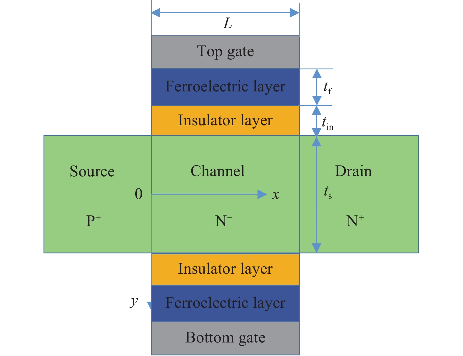
Fig. 1.  (Color online) Structure of the NC DG TFETs with a metal–FE–insulator–semiconductor.

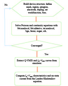
Fig. 2.  (Color online) Flow diagram of the simulation.

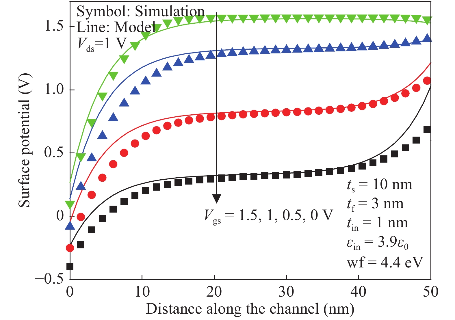
Fig. 3.  (Color online) Surface potential for the proposed TFET with different Vgs.

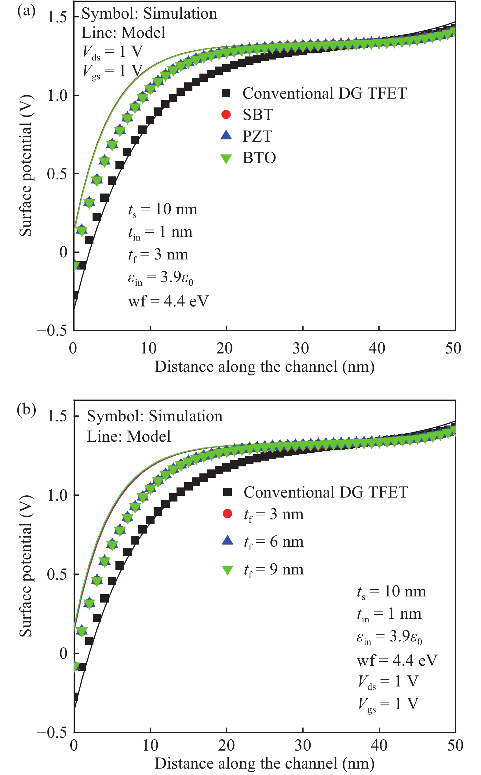
Fig. 4.  (Color online) Surface potential for the TFET (a) with and without ferroelectric layer, (b) with different tf.

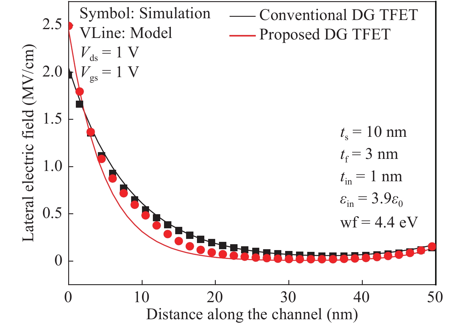
Fig. 5.  (Color online) Lateral electrical field for the DG TFET.

Fig. 6.  (Color online) Shortest tunneling length for different (a) gate–source voltage, (b) thickness of ferroelectric layer.

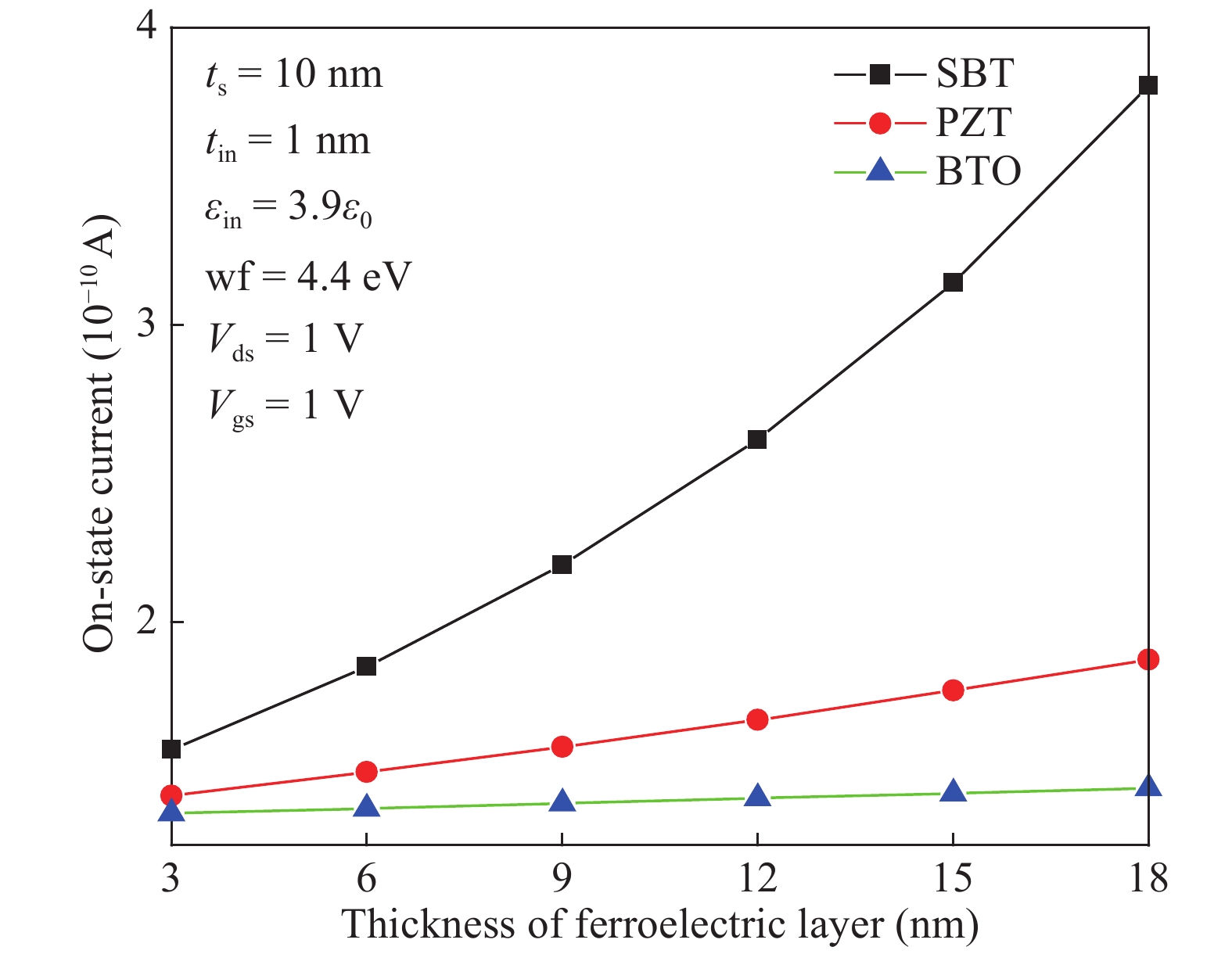
Fig. 7.  (Color online) On-state current for different thickness of ferroelectric layer.

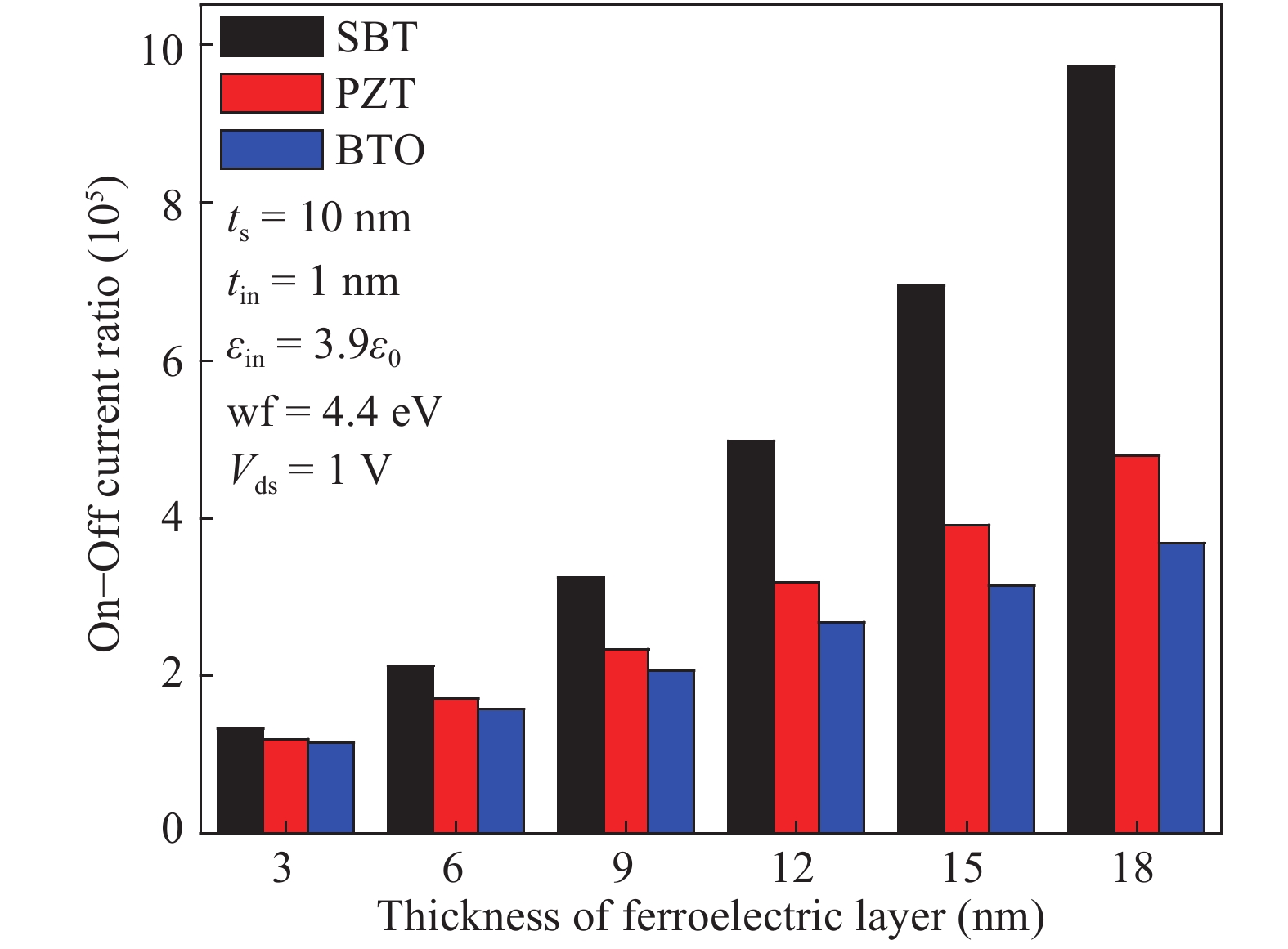
Fig. 8.  (Color online) On–Off current ratio for different thickness of ferroelectric layer.

[1]
Prabhat V, Dutta A K. Analytical surface potential and drain current models of dual-metal-gate double-gate tunnel-FETs. IEEE Trans Electron Devices, 2016, 63(5): 2190 doi: 10.1109/TED.2016.2541181
[2]
Mohammadi S, Khaveh H R T. An analytical model for double-gate tunnel FETs considering the junctions depletion regions and the channel mobile charge carriers. IEEE Trans Electron Devices, 2017, 64(3): 1268
[3]
Nupur N, Abhinav K. Overcoming the drawback of lower sense margin in tunnel FET based dynamic memory along with enhanced charge retention and scalability. Nanotechnology, 2017, 28: 445203 doi: 10.1088/1361-6528/aa8805
[4]
Kumar S, Goel E, Singh K, et al. A compact 2-D analytical model for electrical characteristics of double-gate tunnel field-effect transistors with a SiO2/high-k stacked gate-oxide structure. IEEE Trans Electron Devices, 2016, 63(8): 3291 doi: 10.1109/TED.2016.2572610
[5]
Navjeet B, Subir K S. An analytical model for tunnel barrier modulation in triple metal double gate TFET. IEEE Trans Electron Devices, 2015, 62(7): 2136 doi: 10.1109/TED.2015.2434276
[6]
Hraziia, Vladimirescu A, Amara A, et al. An analysis on the ambipolar current in Si double-gate tunnel FETs. Solid-State Electron, 2012, 70(4): 67
[7]
Wu J Z, Taur Y. Reduction of TFET OFF-current and subthreshold swing by lightly doped drain. IEEE Trans Electron Devices, 2016, 63(8): 3342 doi: 10.1109/TED.2016.2577589
[8]
Nigam K, Pandey S, Kondekar P N, et al. A barrier controlled charge plasma-based tfet with gate engineering for ambipolar suppression and RF/linearity performance improvement. IEEE Trans Electron Devices, 2017, 64(6): 2751 doi: 10.1109/TED.2017.2693679
[9]
Raad B R, Sharma D, Kondekar P, et al. Drain work function engineered doping-less charge plasma TFET for ambipolar suppression and RF performance improvement: A proposal, design, and investigation. IEEE Trans Electron Devices, 2016, 63(10): 3950 doi: 10.1109/TED.2016.2600621
[10]
Ko E, Lee H, Park J D, et al. Vertical tunnel FET: design optimization with triple metal-gate layers. IEEE Trans Electron Devices, 2016, 63(12): 5030 doi: 10.1109/TED.2016.2619372
[11]
Boucart K, Ionescu A M. Double-gate tunnel FET with high-k gate dielectric. IEEE Trans Electron Devices, 2007, 54(7): 1725 doi: 10.1109/TED.2007.899389
[12]
Kao K H, Verhulst A S, Vandenberghe W G, et al. Direct and indirect band-to-band tunneling in germanium-based TFETs. IEEE Trans Electron Devices, 2012, 59(2): 292 doi: 10.1109/TED.2011.2175228
[13]
Ahish S, Sharma D, Kumar Y B N, et al. Performance enhancement of novel InAs/Si hetero double-gate tunnel FET using gaussian doping. IEEE Trans Electron Devices, 2016, 63(1): 288 doi: 10.1109/TED.2015.2503141
[14]
Yadav D S, Sharma D, Kumar A, et al. Performance investigation of hetero material (InAs/Si)-based charge plasma TFET. Micro Nano Lett, 2017, 12(6): 358 doi: 10.1049/mnl.2016.0688
[15]
Bagga N, Dasgupta S. Surface potential and drain current analytical model of gate all around triple metal TFET. IEEE Trans Electron Devices, 2017, 64(2): 606 doi: 10.1109/TED.2016.2642165
[16]
Abdi D B, Kumar M J. 2-D Threshold voltage model for the double-gate p–n–p–n TFET with localized charges. IEEE Trans Electron Devices, 2016, 63(9): 3663 doi: 10.1109/TED.2016.2589927
[17]
Wang Y B, Han G Q, Liu Y, et al. Investigation of GaAsBi/GaAsN type-II staggered heterojunction TFETs with the analytical model. IEEE Trans Electron Devices, 2017, 64(4): 1541 doi: 10.1109/TED.2017.2668063
[18]
Xu H F, Guan B G. Two-dimensional analytical model for hetero-junction double-gate tunnel field-effect transistor with a stacked gate-oxide structure. Jpn J Appl Phys, 2017, 56(5): 054201 doi: 10.7567/JJAP.56.054201
[19]
Zhao Y, Wu C L, Huang Q Q, et al. A novel tunnel FET design through adaptive bandgap engineering with constant sub-threshold slope over 5 decades of current and high ION/IOFF ratio. IEEE Electron Device Lett, 2017, 38(5): 540 doi: 10.1109/LED.2017.2679031
[20]
Kondekar P N, Nigam K, Pandey S, et al. Design and analysis of polarity controlled electrically doped tunnel FET with bandgap engineering for analog/RF applications. IEEE Trans Electron Devices, 2017, 64(2): 412 doi: 10.1109/TED.2016.2637638
[21]
Lahgere A, Panchore M, Singh J. Dopingless ferroelectric tunnel FET architecture for the improvement of performance of dopingless n-channel tunnel FETs. Superlattices Microstruct, 2016, 96: 16 doi: 10.1016/j.spmi.2016.05.004
[22]
Kale S, Kondekar P N. Ferroelectric Schottky barrier tunnel FET with gate-drain underlap: Proposal and investigation. Superlattices Microstruct., 2016, 89: 225.
[23]
Lee M H, Wei Y T, Lin J C, et al. Ferroelectric gate tunnel field-effect transistors with low-power steep turn-on. AIP Adv, 2014, 4(10): 107117 doi: 10.1063/1.4898150
[24]
Kobayashi M, Jang K, Ueyama N, et al. Negative capacitance for boosting tunnel FET performance. IEEE Trans Nanotechnol, 2017, 16(2): 253 doi: 10.1109/TNANO.2017.2658688
[25]
Liu C, Chen P G, Xie M J, et al. Simulation-based study of negative-capacitance double-gate tunnel field-effect transistor with ferroelectric gate stack. Jpn J Appl Phys, 2016, 55(4S): 04EB08 doi: 10.7567/JJAP.55.04EB08
[26]
Saeidi A, Biswas A, Ionescu A M. Modeling and simulation of low power ferroelectric non-volatile memory tunnel field effect transistors using silicon-doped hafnium oxide as gate dielectric. Solid-State Electron, 2016, 124(10): 16
[27]
Chowdhury N, Azad S M F, Khosru Q D M. Negative capacitance tunnel field effect transistor: A novel device with low subthreshold swing and high on current. ECS Trans, 2014, 58(16): 1 doi: 10.1149/05816.0001ecst
[28]
Chowdhury N, Ahmed I, Fakhrul T, et al. A low subthreshold swing tunneling field effect transistor for next generation low power CMOS applications. Physica E, 2015, 74(11): 251
[29]
Jiang C S, Liang R R, Xu J. Investigation of negative capacitance gate-all-around tunnel FETs combining numerical simulation and analytical modeling. IEEE Trans Nanotechnol, 2017, 16(1): 58
[30]
ATLAS User’s Manual (Silvaco Int., Santa Clara, CA, 2012).
[31]
Girish P, Tapas D, Amit A, et al. Compact model for ferroelectric negative capacitance transistor with MFIS structure. IEEE Trans Electron Devices, 2017, 64(3): 1366 doi: 10.1109/TED.2017.2654066
[32]
Cheng I L, Asif I K, Sayeef S, et al. Effects of the variation of ferroelectric properties on negative capacitance FET characteristics. IEEE Trans Electron Devices, 2016, 63(5): 2197 doi: 10.1109/TED.2016.2514783
  • Search

    Advanced Search >>

    GET CITATION

    shu

    Export: BibTex EndNote

    Article Metrics

    Article views: 5127 Times PDF downloads: 144 Times Cited by: 0 Times

    History

    Received: 01 January 2018 Revised: Online: Uncorrected proof: 23 May 2018Published: 09 October 2018

    Catalog

      Email This Article

      User name:
      Email:*请输入正确邮箱
      Code:*验证码错误
      Huifang Xu. Two dimensional analytical model for a negative capacitance double gate tunnel field effect transistor with ferroelectric gate dielectric[J]. Journal of Semiconductors, 2018, 39(10): 104004. doi: 10.1088/1674-4926/39/10/104004 H F Xu, Two dimensional analytical model for a negative capacitance double gate tunnel field effect transistor with ferroelectric gate dielectric[J]. J. Semicond., 2018, 39(10): 104004. doi: 10.1088/1674-4926/39/10/104004.Export: BibTex EndNote
      Citation:
      Huifang Xu. Two dimensional analytical model for a negative capacitance double gate tunnel field effect transistor with ferroelectric gate dielectric[J]. Journal of Semiconductors, 2018, 39(10): 104004. doi: 10.1088/1674-4926/39/10/104004

      H F Xu, Two dimensional analytical model for a negative capacitance double gate tunnel field effect transistor with ferroelectric gate dielectric[J]. J. Semicond., 2018, 39(10): 104004. doi: 10.1088/1674-4926/39/10/104004.
      Export: BibTex EndNote

      Two dimensional analytical model for a negative capacitance double gate tunnel field effect transistor with ferroelectric gate dielectric

      doi: 10.1088/1674-4926/39/10/104004
      Funds:

      Project supported by the University Natural Science Research Key Project of Anhui Province (No. KJ2017A502), the Talents Project of Anhui Science and Technology University (No. DQYJ201603), and the Excellent Talents Supported Project of Colleges and Universities (No. gxyq2018048).

      More Information
      • Corresponding author: xu0342@163.com
      • Received Date: 2018-01-01
      • Accepted Date: 2018-01-01
      • Published Date: 2018-10-01

      Catalog

        /

        DownLoad:  Full-Size Img  PowerPoint
        Return
        Return