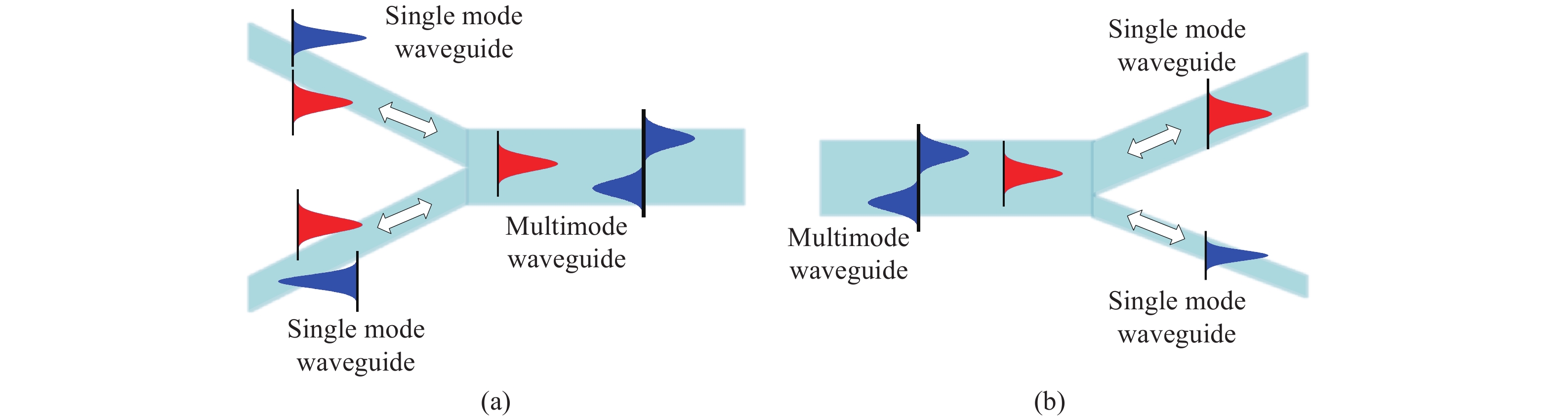
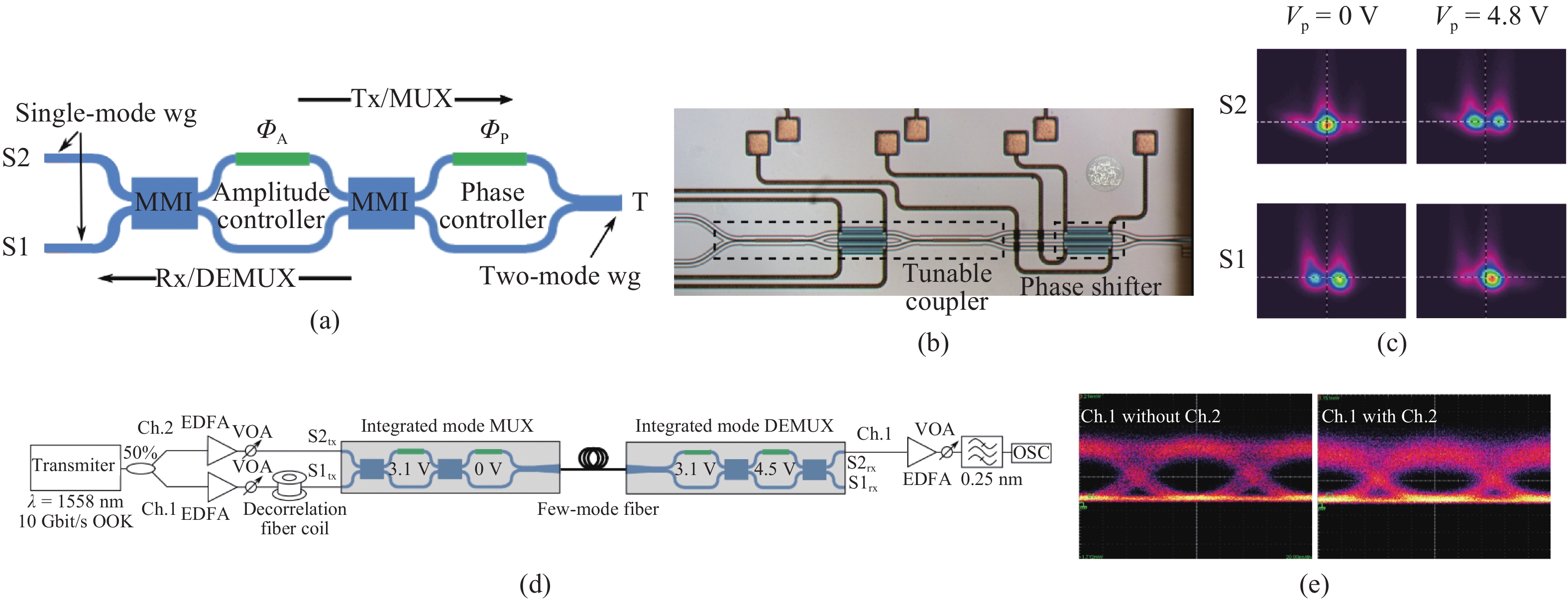
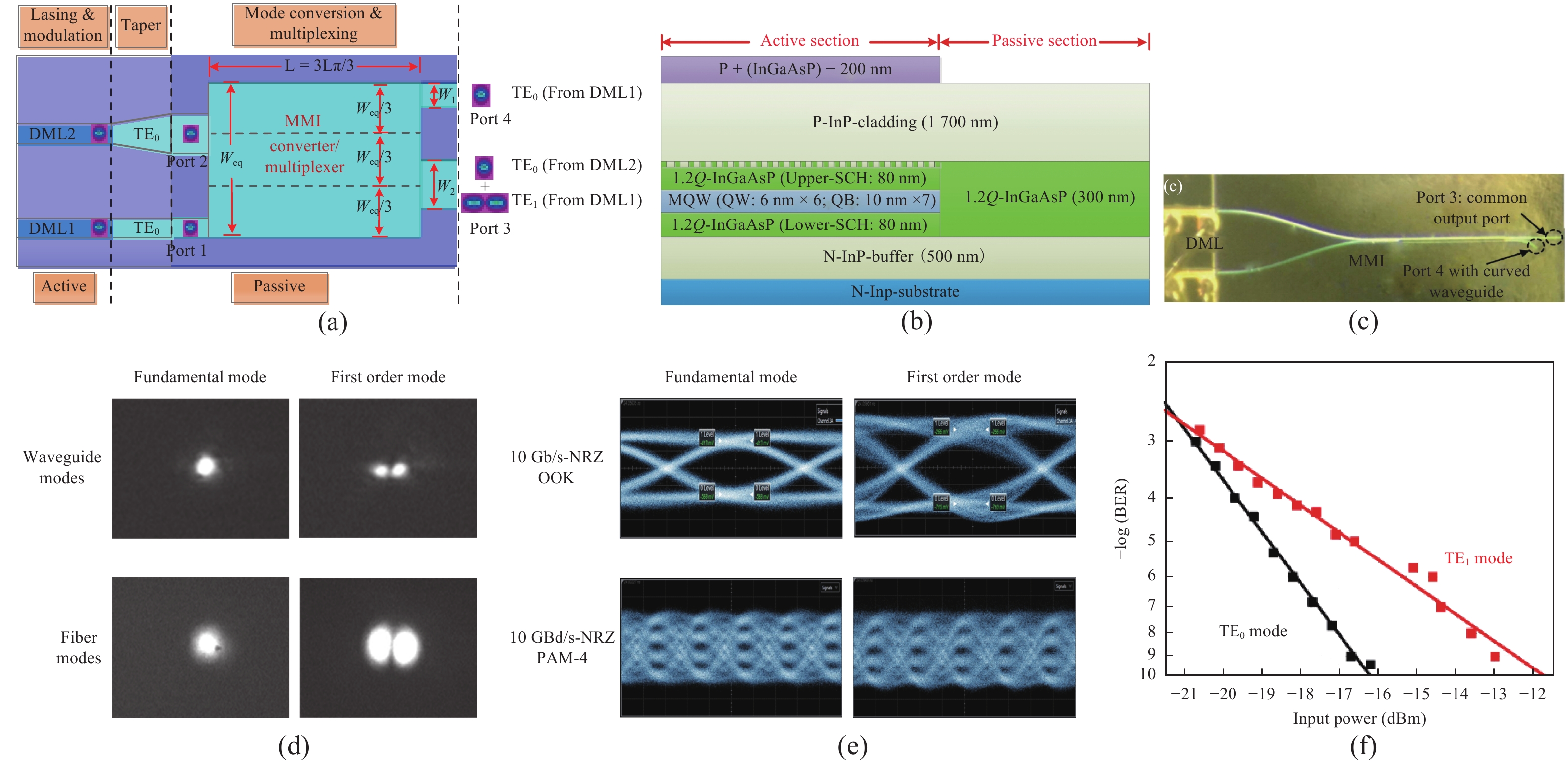
Mode-division multiplexing (MDM) has become an increasingly important technology to further increase the transmission capacity of both optical-fiber-based communication networks, data centers and waveguide-based on-chip optical interconnects. Mode manipulation devices are indispensable in MDM system and have been widely studied in fiber, planar lightwave circuits, and silicon and InP based platforms. InP-based integration technology provides the easiest accessibility to bring together the functions of laser sources, modulators, and mode manipulation devices into a single chip, making it a promising solution for fully integrated few-mode transmitters in the MDM system. This paper reviews the recent progress in InP-based mode manipulation devices, including the few-mode converters, multiplexers, demultiplexers, and transmitters. The working principle, structures, and performance of InP-based few-mode devices are discussed.


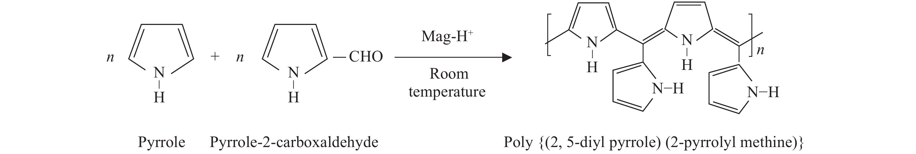
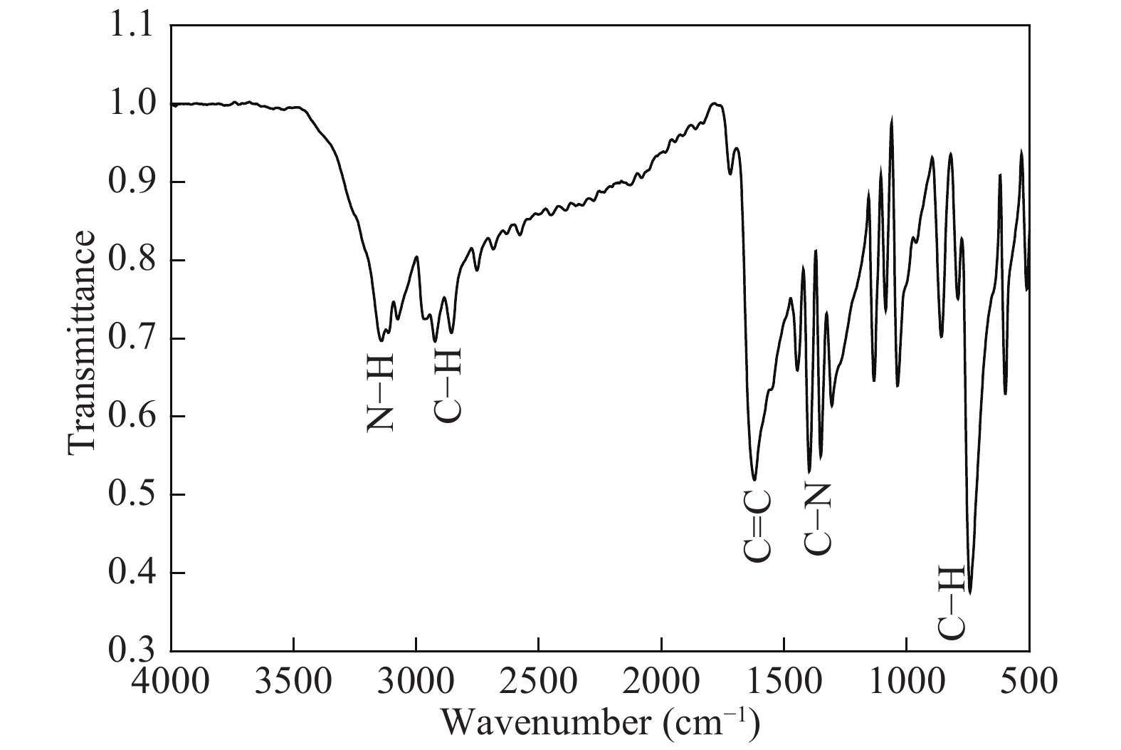
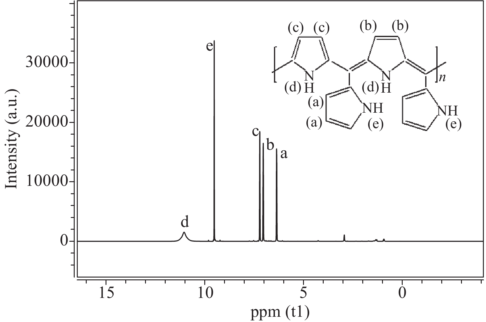
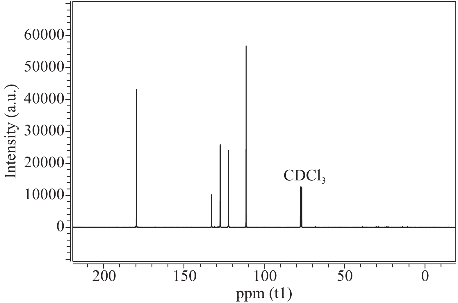
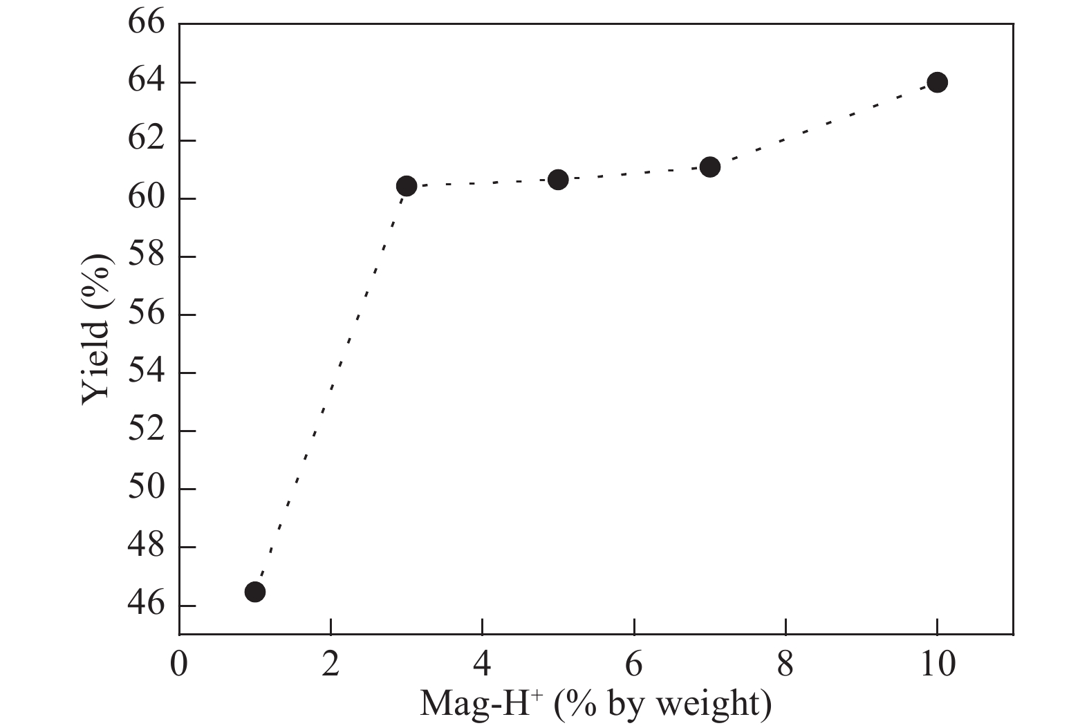
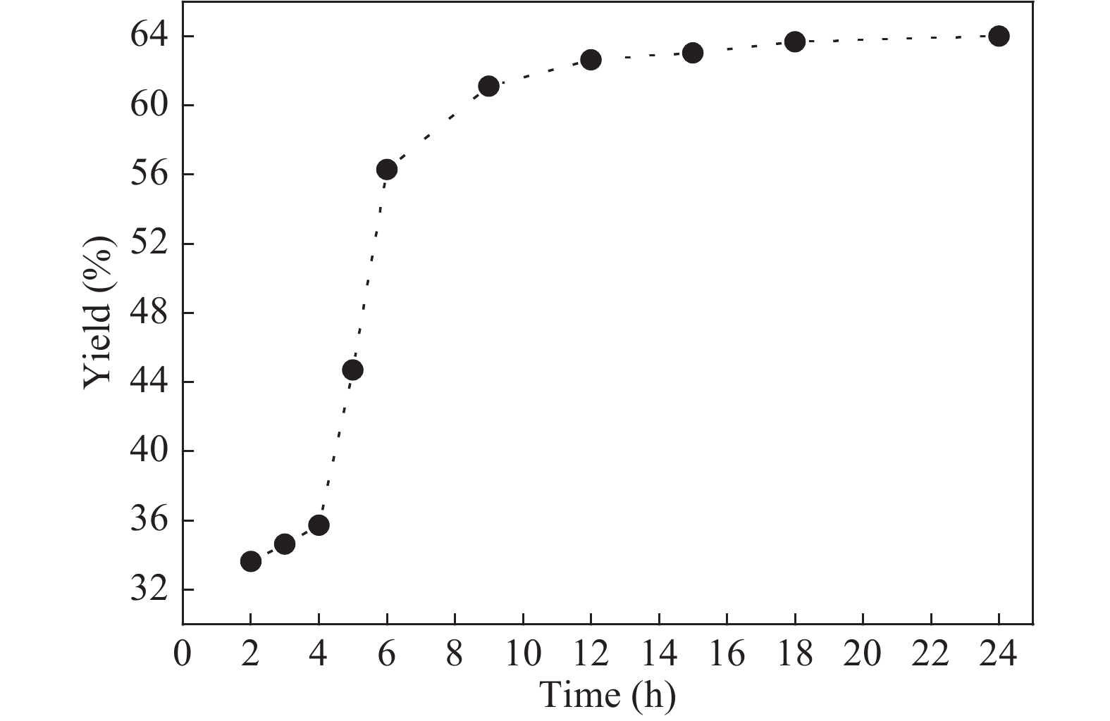
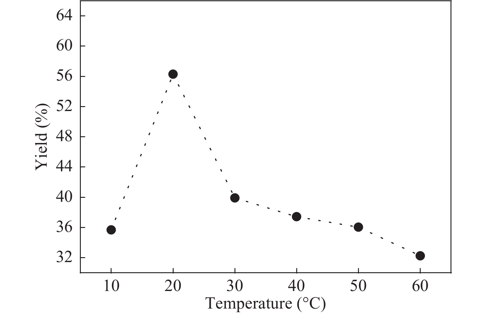
The proposed technique to synthesise poly {(2,5-diyl pyrrole) (2-pyrrolyl methine)} (PPPM) copolymer by condensation of pyrrole and pyrrole-2-carboxaldehyde monomers catalyzed by Maghnite-H+ is introduced. The protons are exchanged with Maghnite-H+, which is available in the form of a montmorillonite silicate clay sheet. The effect of several parameters such as time and temperature of copolymerization, [pyrrole]/[pyrrole-2-carboxaldehyde] molar ratio, amount of Maghnite-H+, and solvent on the produced poly (2,5-diyl pyrrole-2-pyrrolyl methine) semiconductor copolymer material (yield%) was investigated. The synthesized PPPM copolymer was characterized using nuclear magnetic resonance, Fourier transform infrared, and ultraviolet–visible spectroscopy. The results show that the synthesized copolymer using the copolymerization technique is a real organic copolymer consisting of two monomers units (i.e, pyrrole and pyrrole-2-carboxaldehyde). Also, the synthesized copolymer is more soluble than polypyrrole in most of the commonly used organic solvents. Hence, copolymerization of pyrrole with pyrrole-2-carboxaldehyde will overcome the insolubility of polypyrrole. In addition, the resultant copolymer exhibits good film formability. The produced copolymer has several potential applications in the field of rechargeable batteries, sensors, capacitors, light emitting diodes, optical displays, and solar cells.


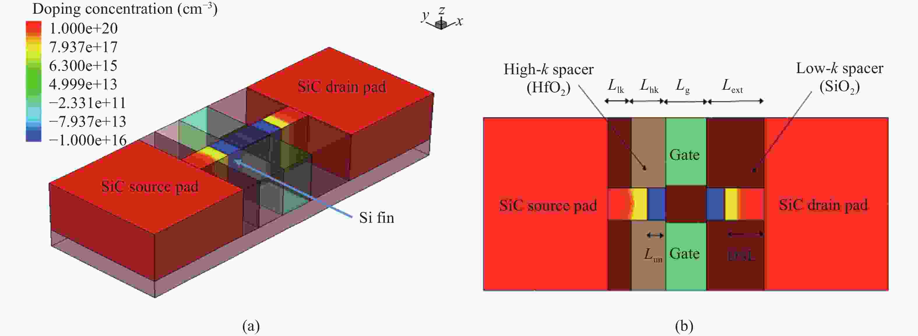
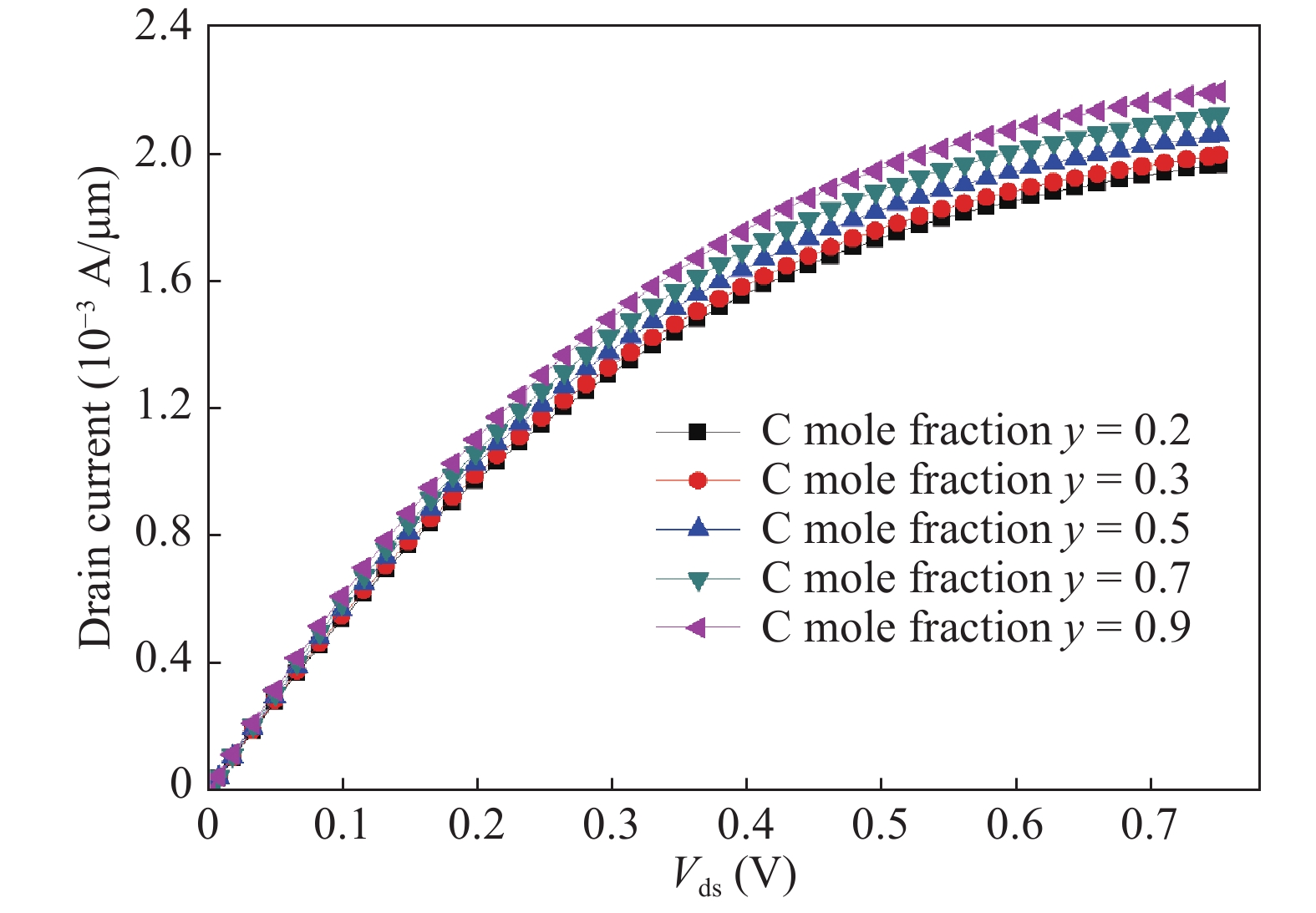
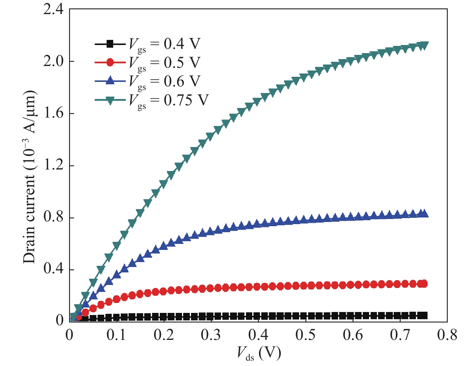
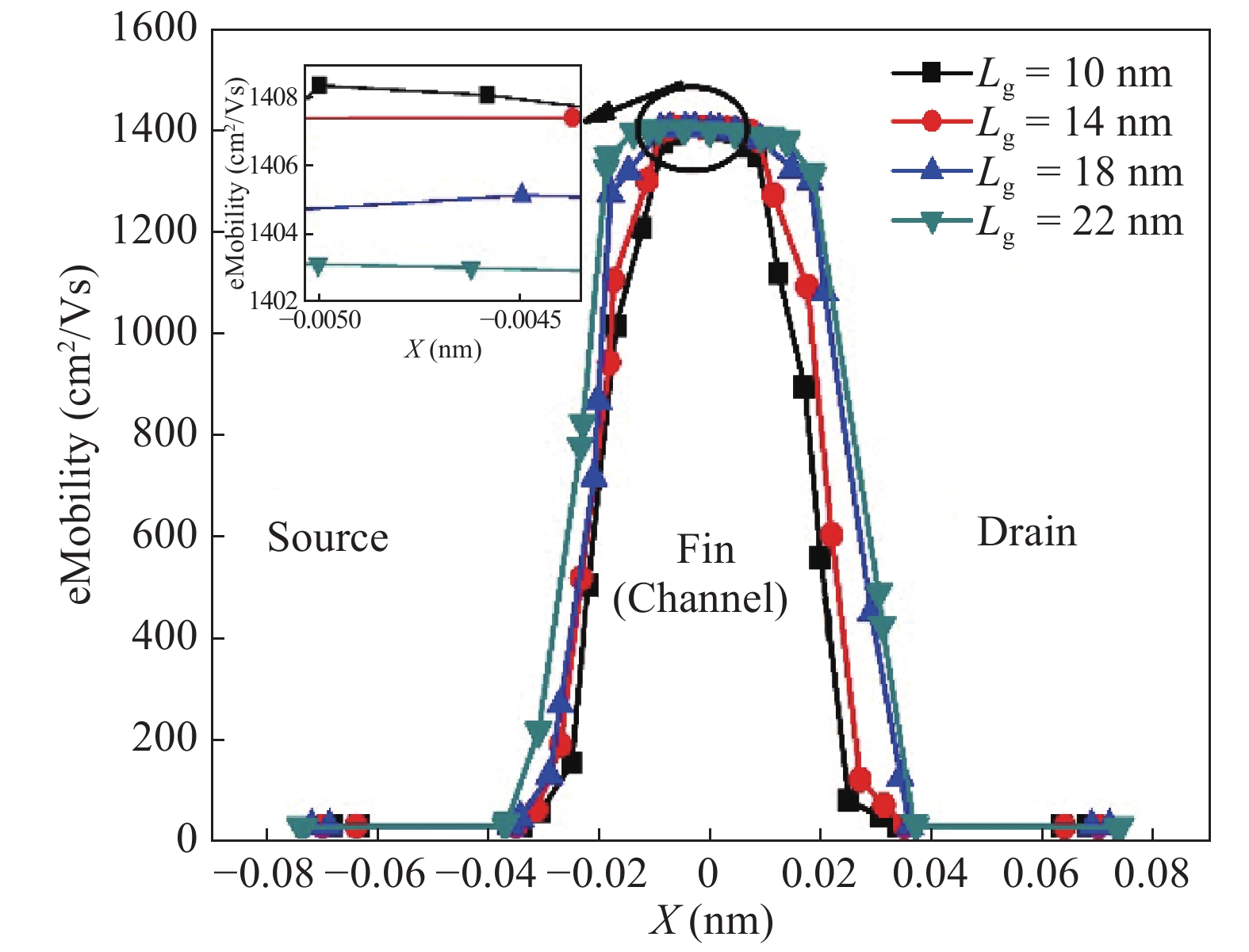
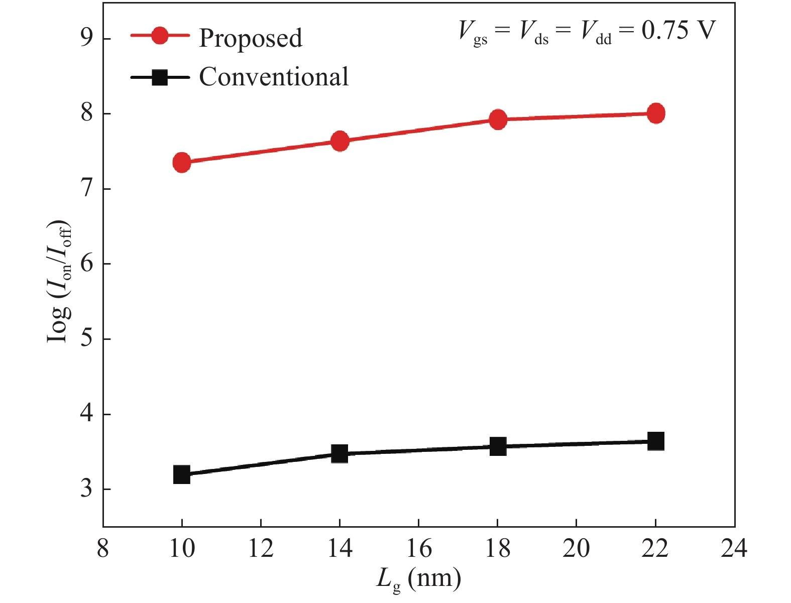
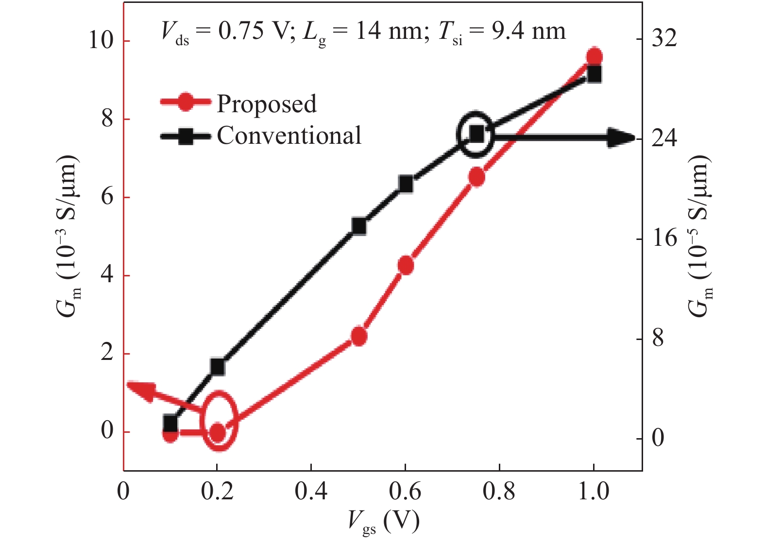
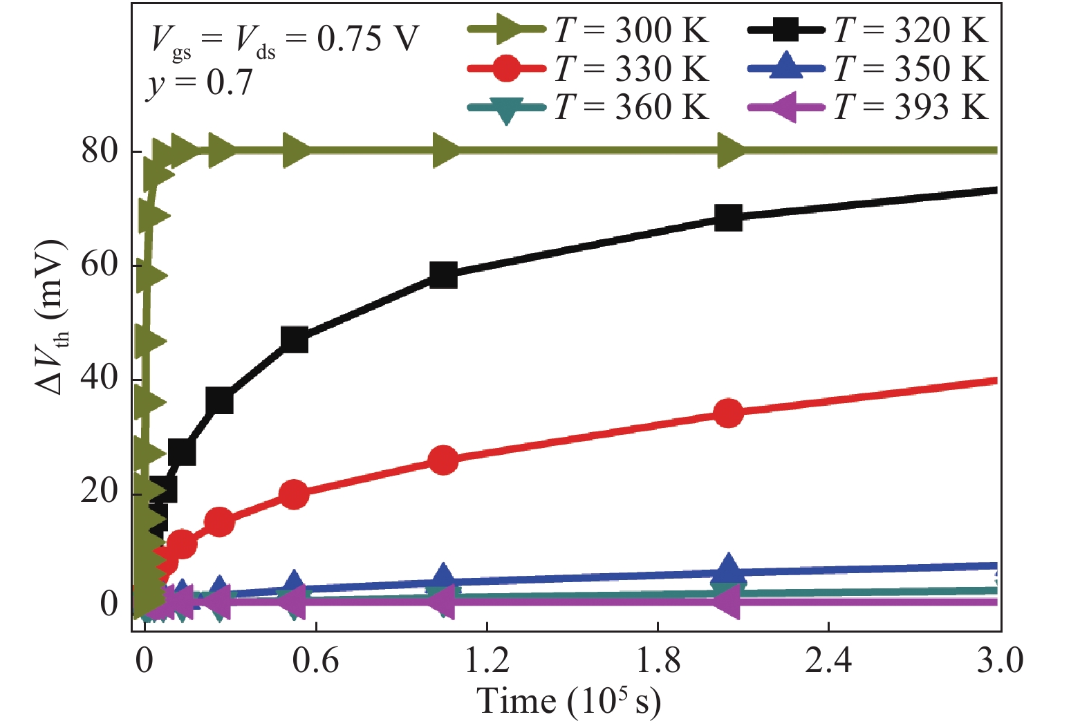
We propose a reliable asymmetric dual-k spacer with SiC source/drain (S/D) pocket as a stressor for a Si channel. This enhances the device performance in terms of electron mobility (eMobility), current driving capabilities, transconductance (Gm) and subthreshold slope (SS). The improved performance is an amalgamation of longitudinal tensile stress along the channel and reduced series resistance. We analysed the variation in drive current for different values of carbon (C) mole fraction y in Si1−yCy. It is found that the mole fraction also helps to improve device lifetime, performance enhancement also pointed by transconductance variation with the gate length. All the simulations are performed in the 3-D Sentaurus TCAD tool. The proposed device structure achieved ION = 2.17 mA/μm for Si0.3C0.7 and found that Si0.5C0.5 is more suitable for the perspective of a process variation effect for 14 nm as the gate length. We introduce reliability issues and their solutions for Si1−yCy FinFET for the first time.


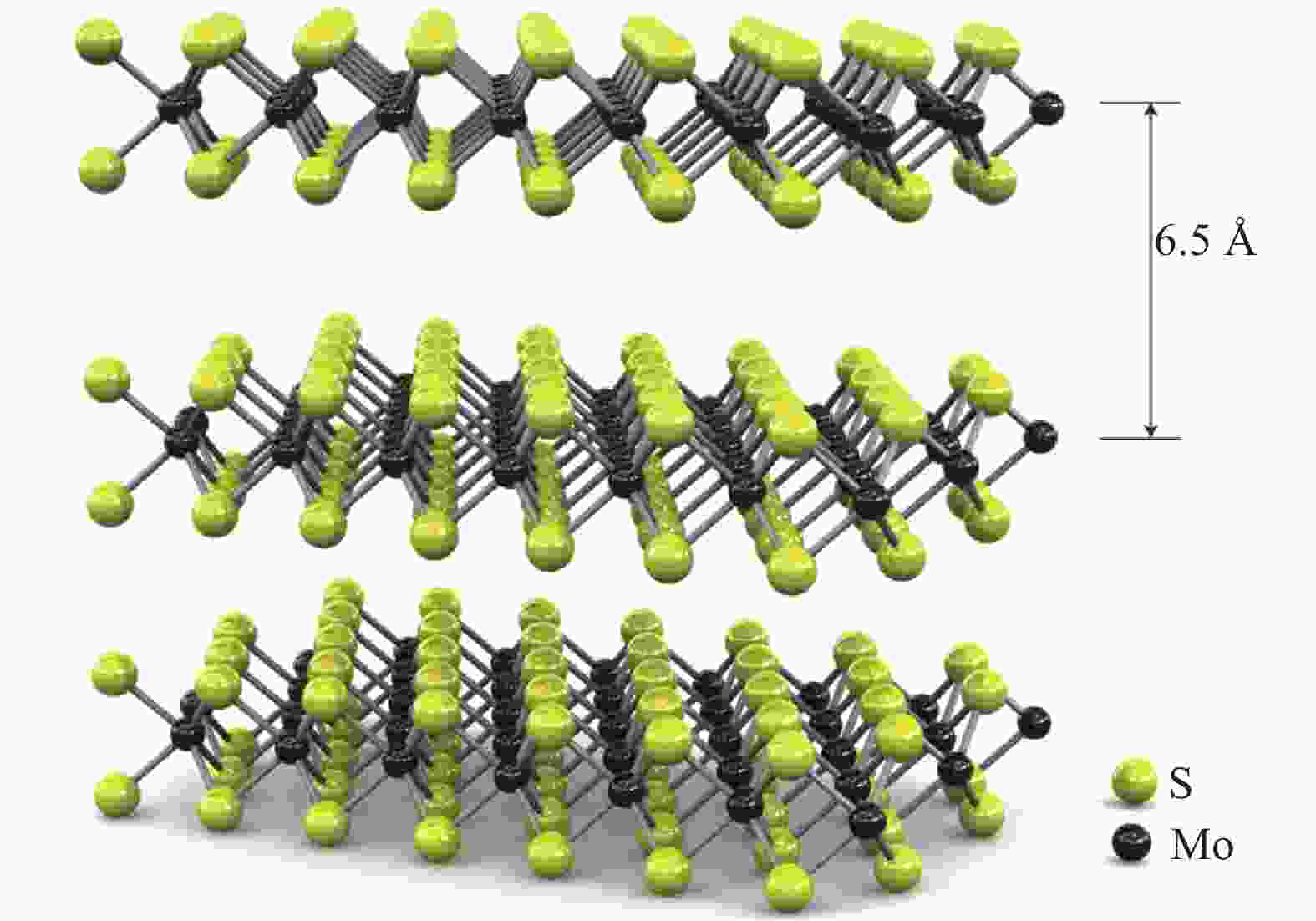
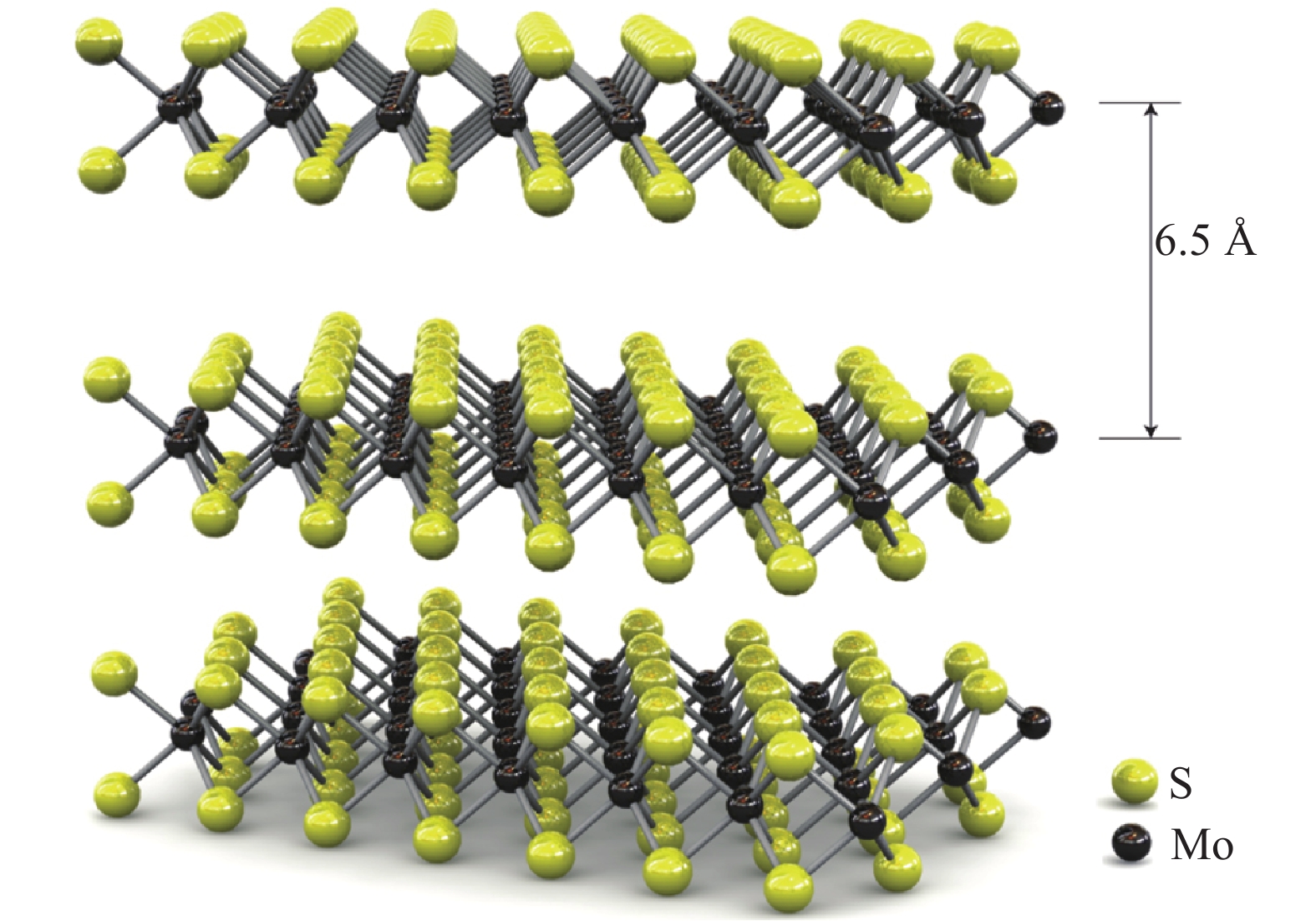
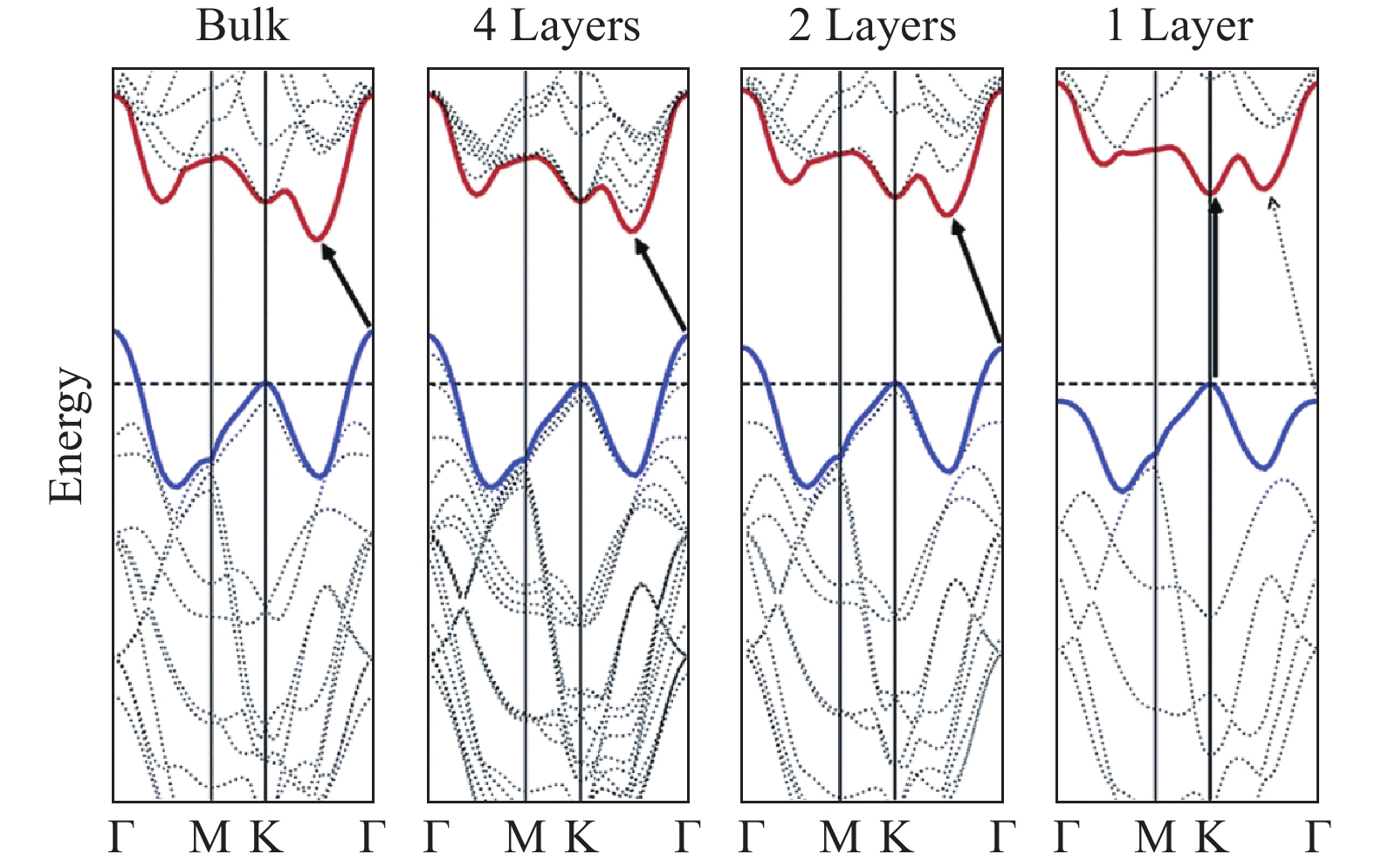
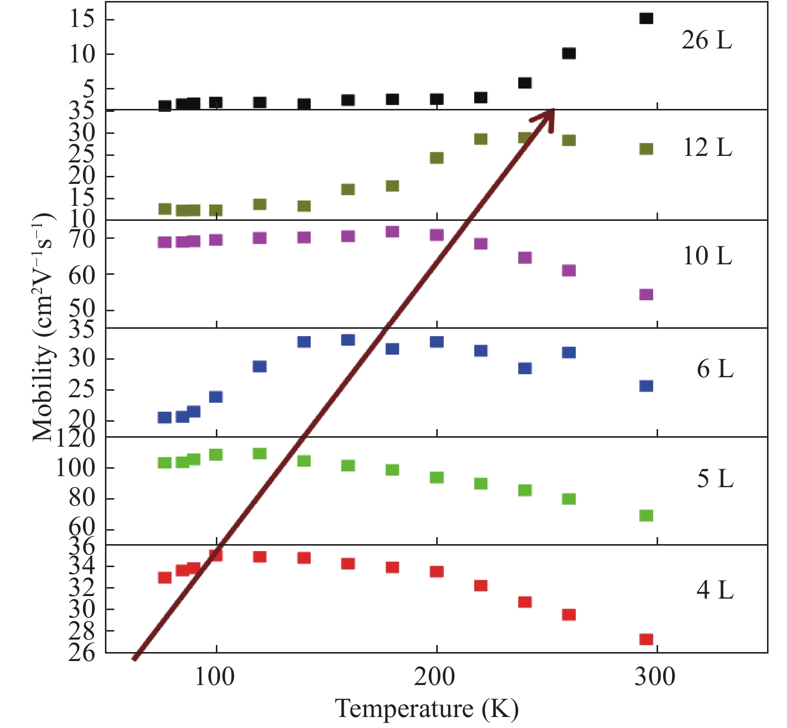
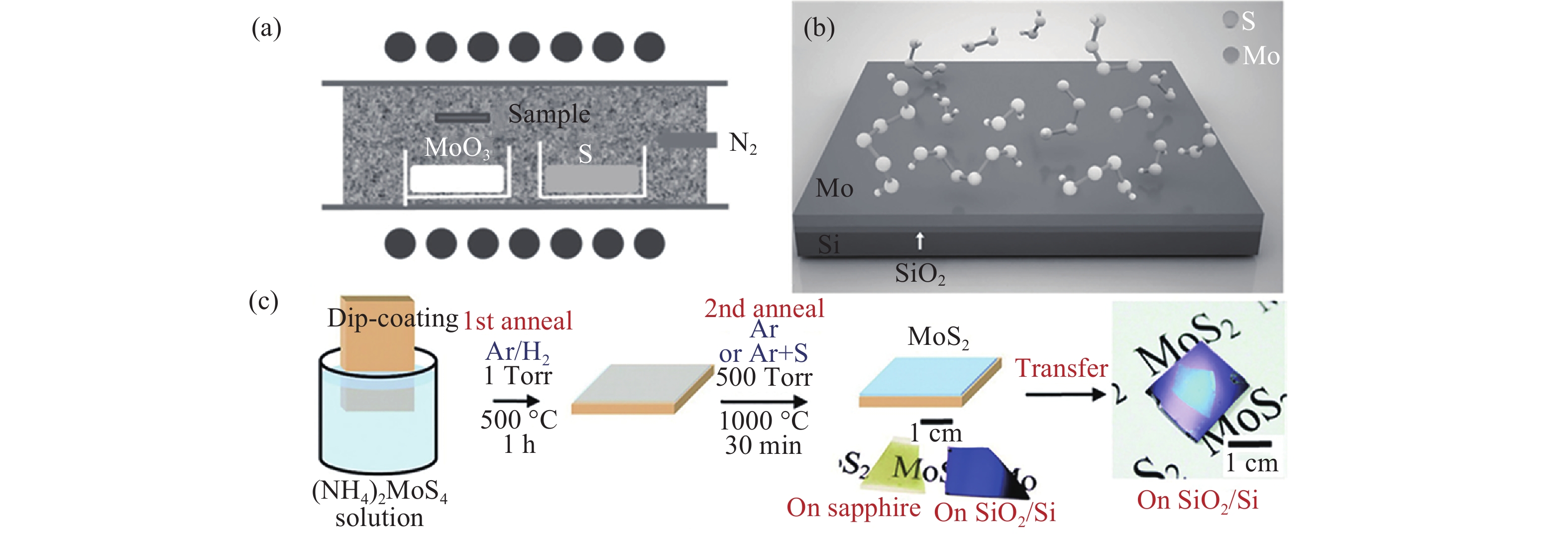
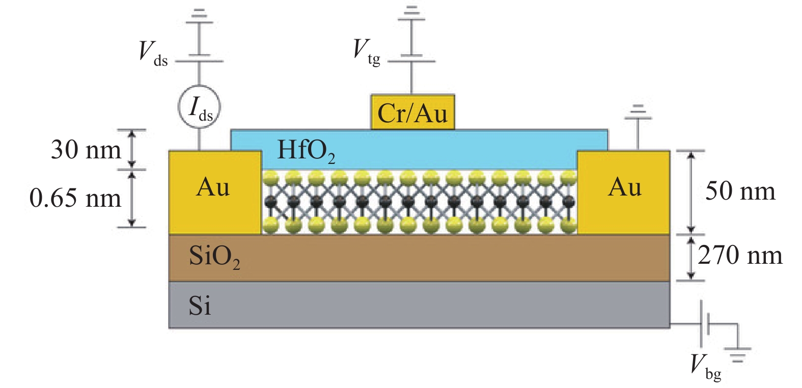
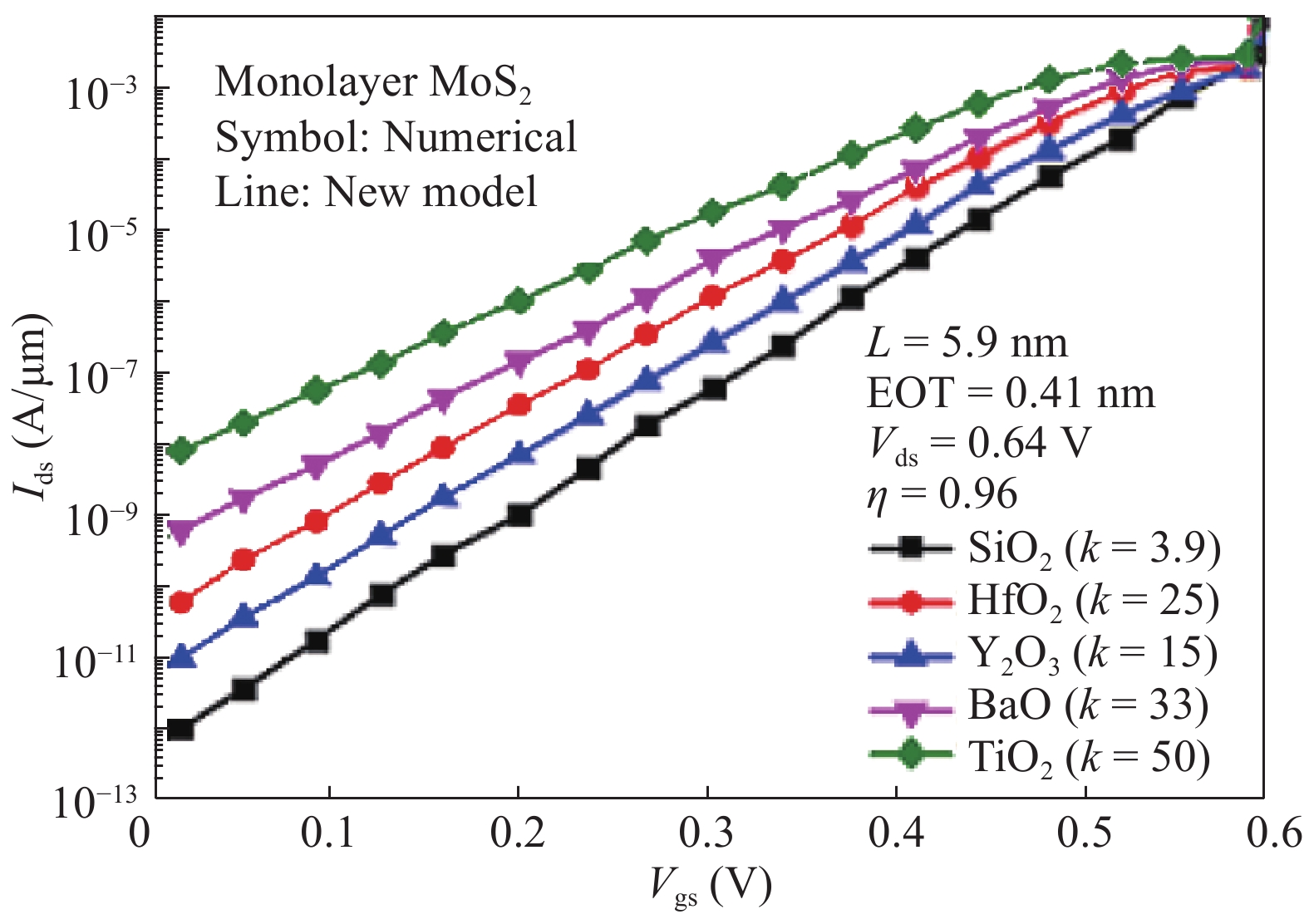
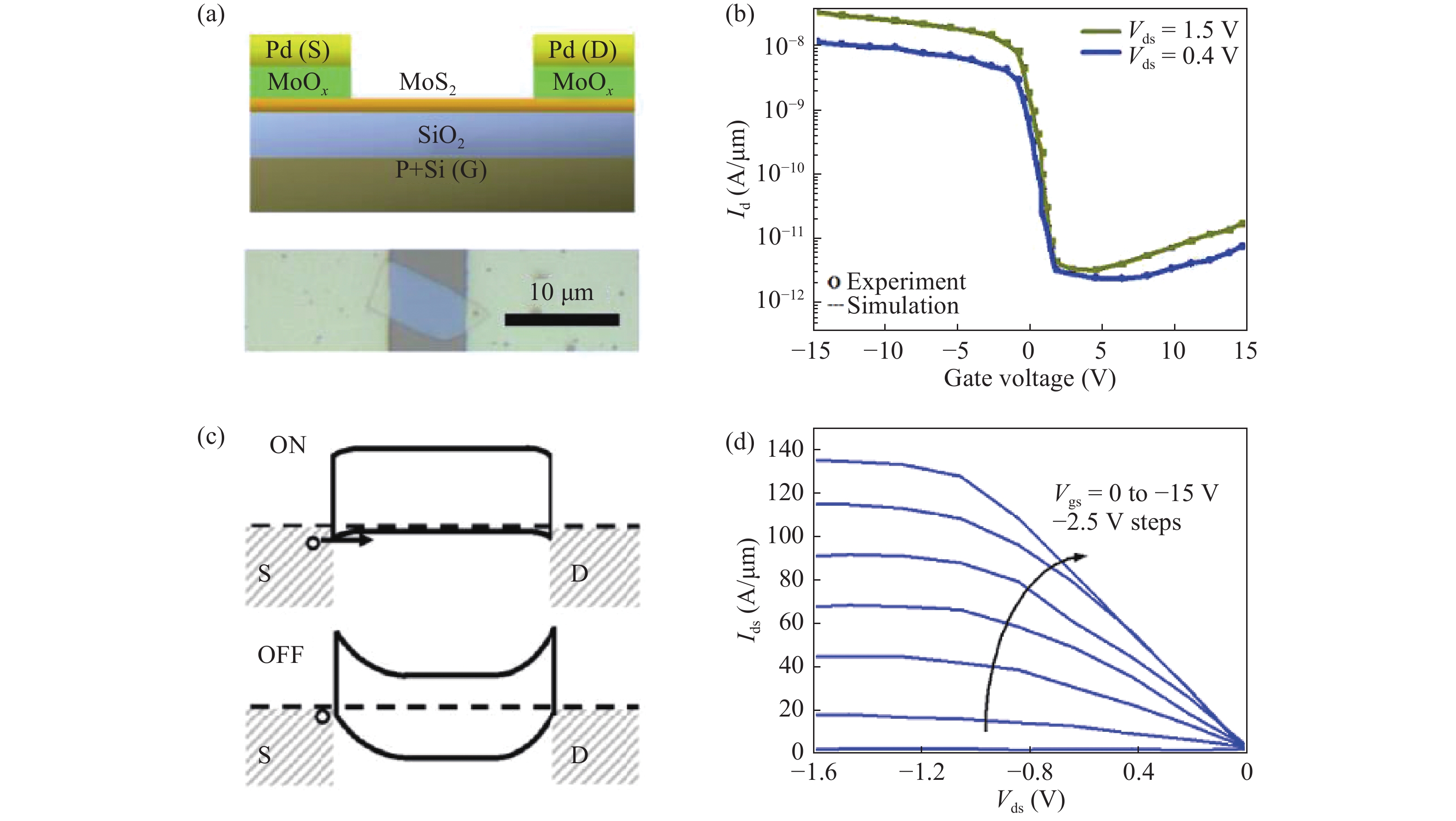
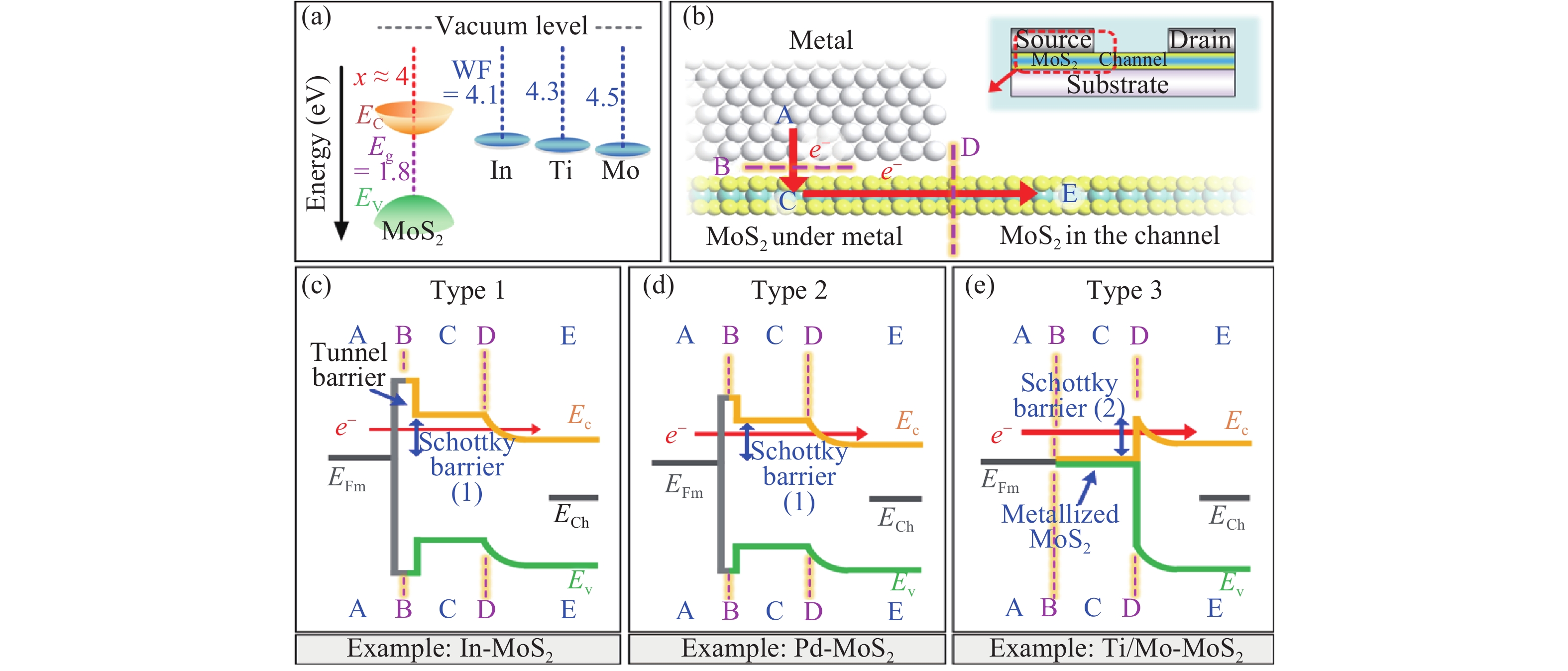
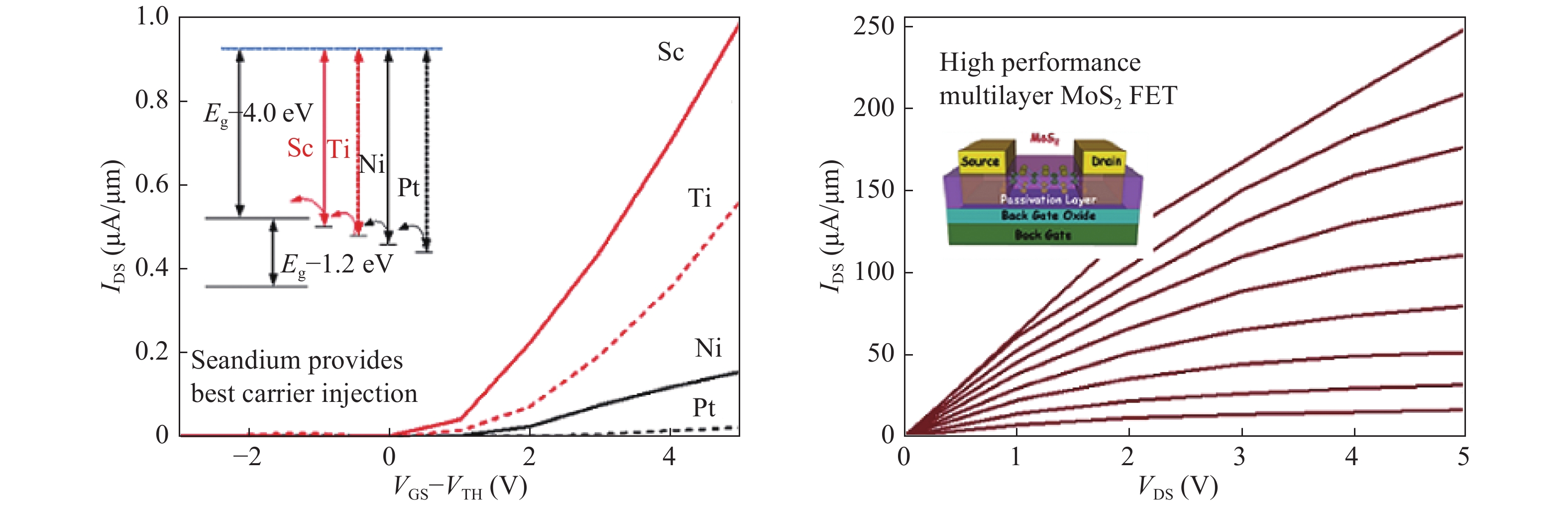
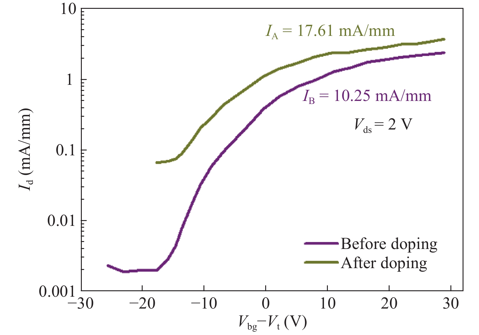
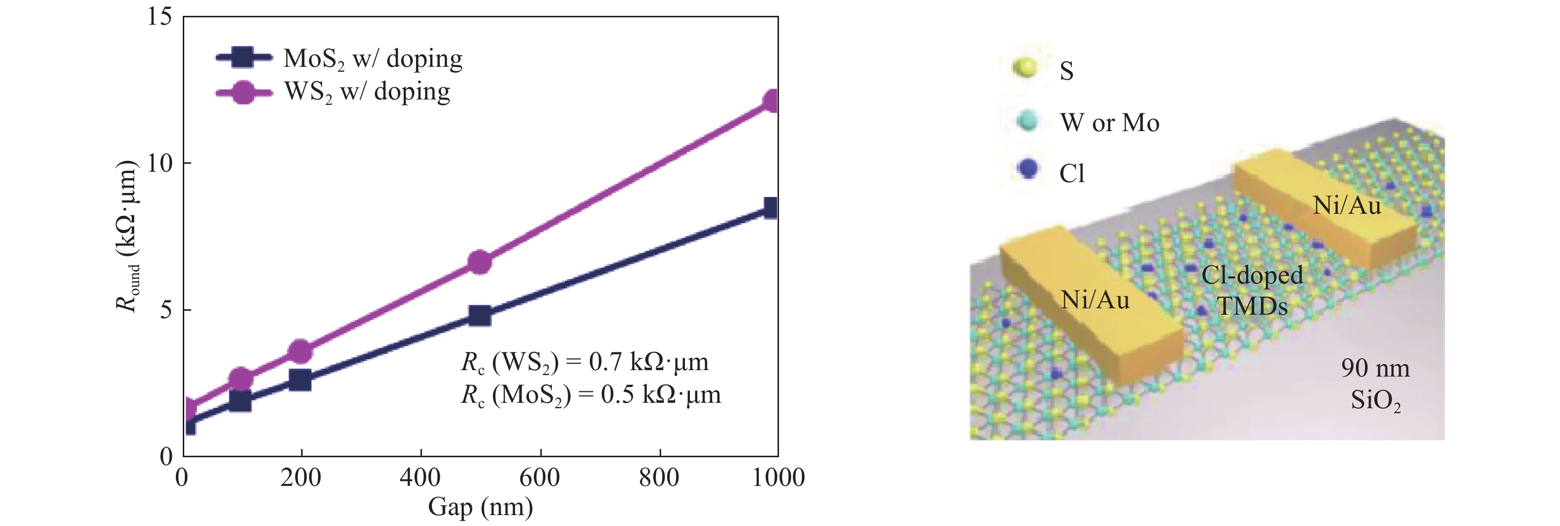
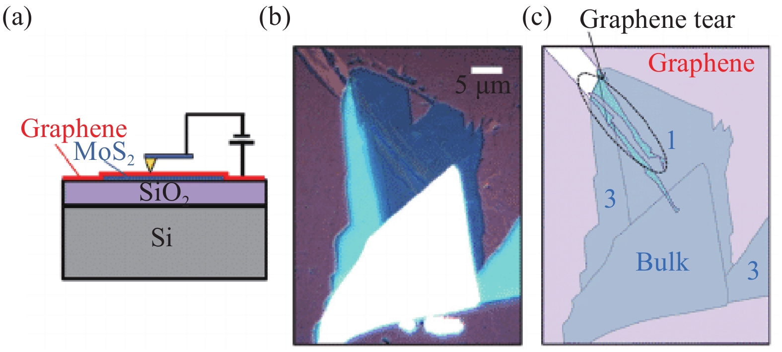
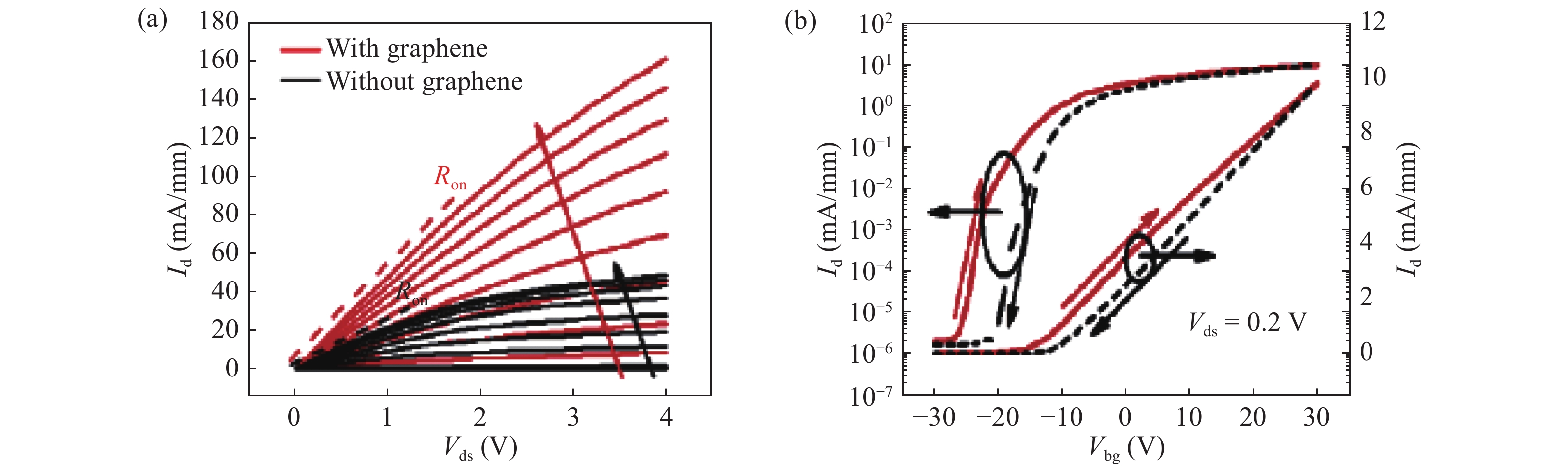
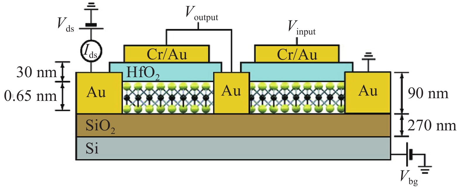
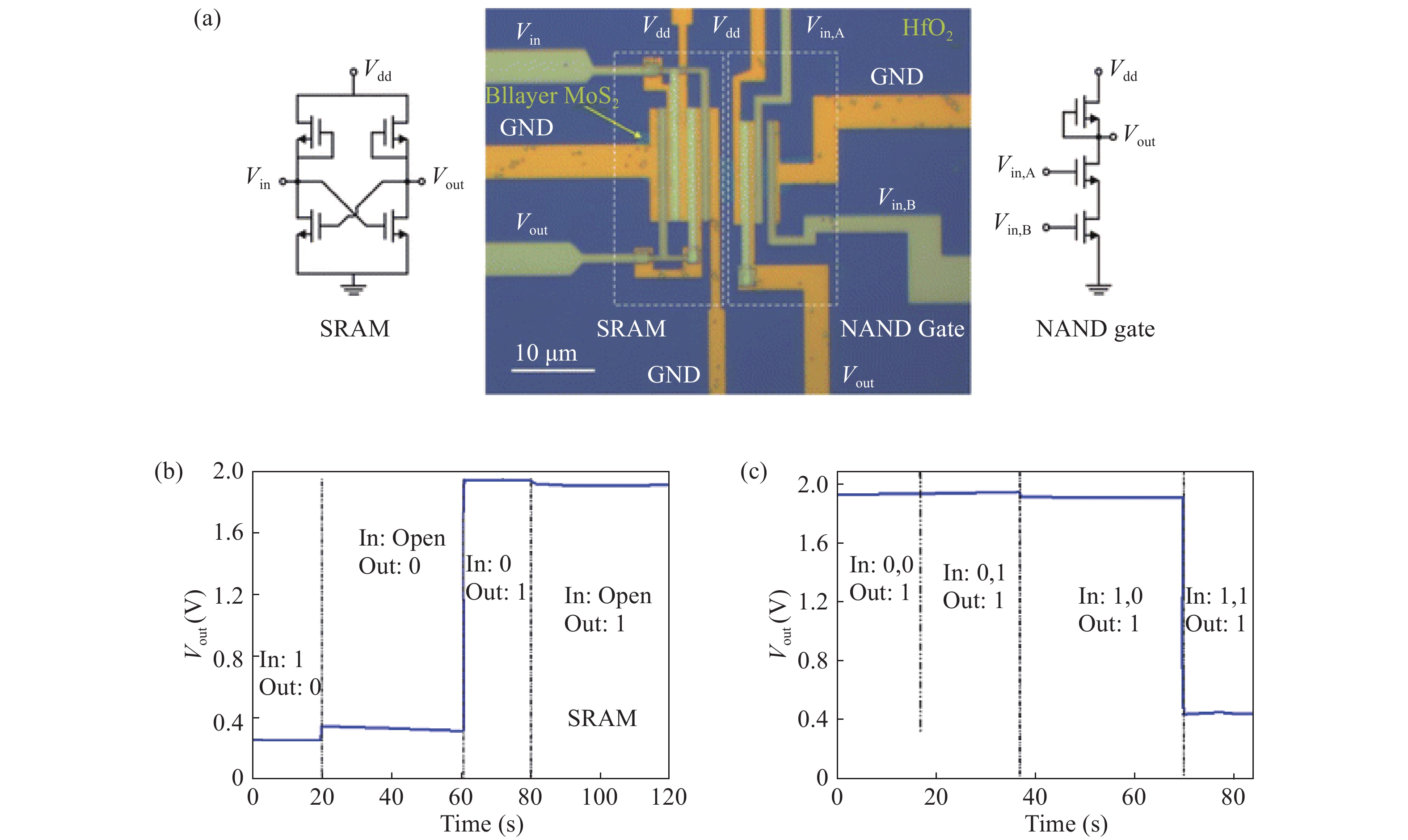
This review paper gives an outline of the recent research progress and challenges of 2D TMDs material MoS2 based device, that leads to an interesting path towards approaching the electronic applications due to its sizeable band gap. This review presents the improvement of MoS2 material as an alternate to a silicon channel in a transistor with its excellent energy band gap, thermal conductivity, and exclusive physical properties that are expected to draw attention to focusing on semiconducting devices for most futuristic applications. We discuss the band structure of MoS2 for a different number of layers with its structure, and various synthesis techniques of the MoS2 layer are also reviewed. The MoS2 based field effect transistor has attracted a great deal of attention due to its excellent properties such as mobility, on/off current ratio, and maximum on-current of the devices. The transition of mobility as a function of temperature and thickness dependence are also discussed. However, the mobility of MoS2 material is large in bulk form and lower in monolayer form. The use of a high-k gate dielectric in MoS2 FET is used to enhance the mobility of the device. Different metal contact engineering and different doping techniques were deployed to achieve low contact resistance. This review paper focuses on various aspects of layered TMDs material MoS2 based field effect transistors.


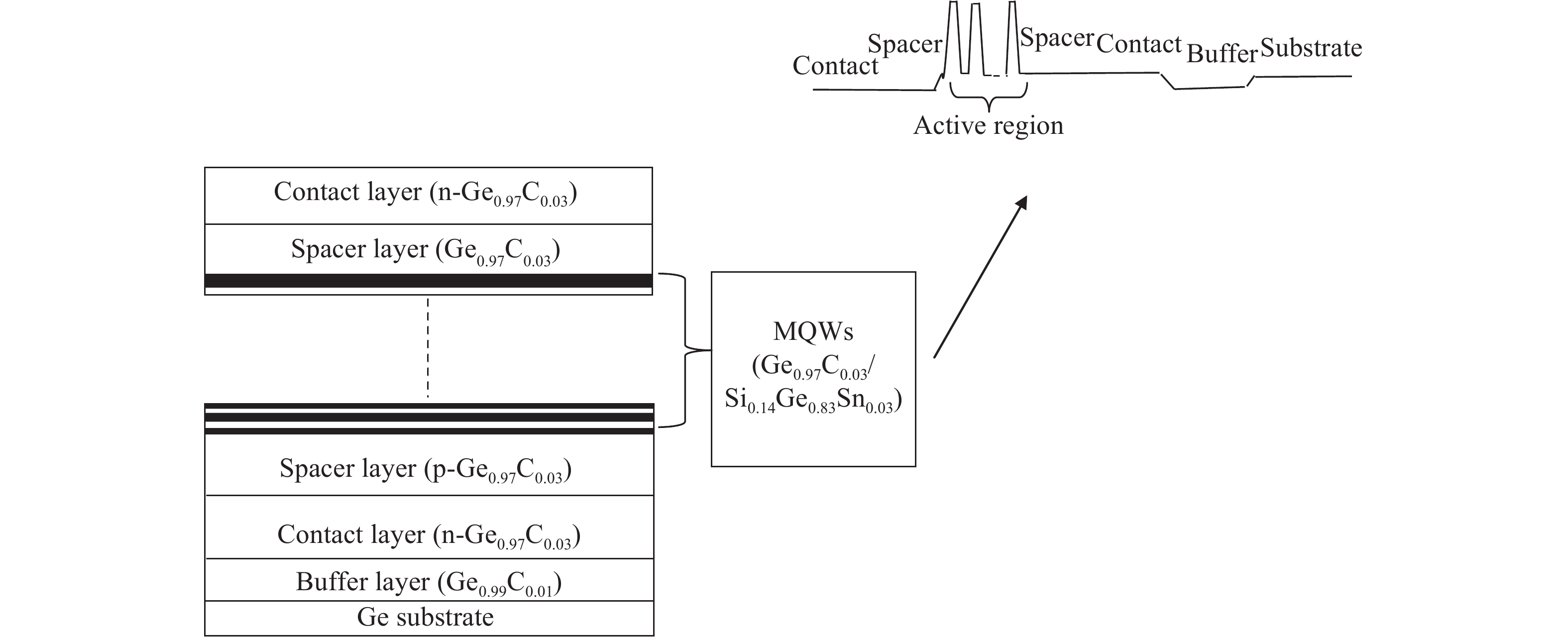
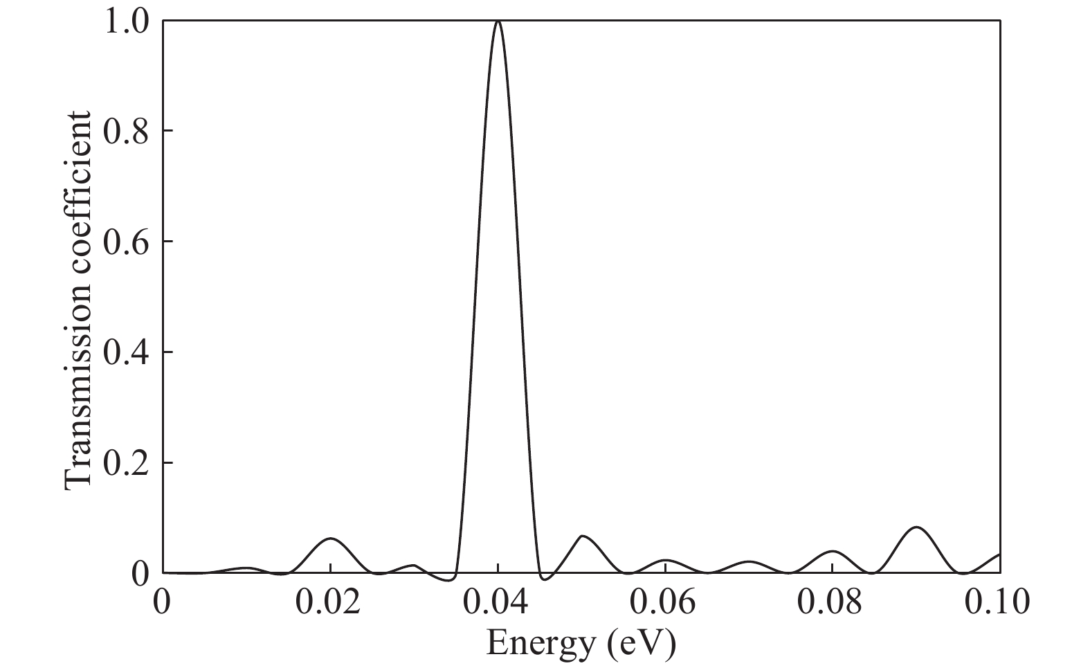
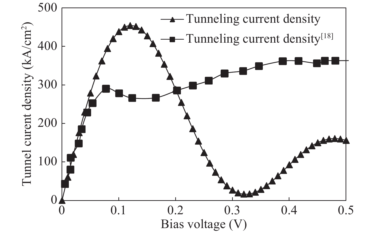
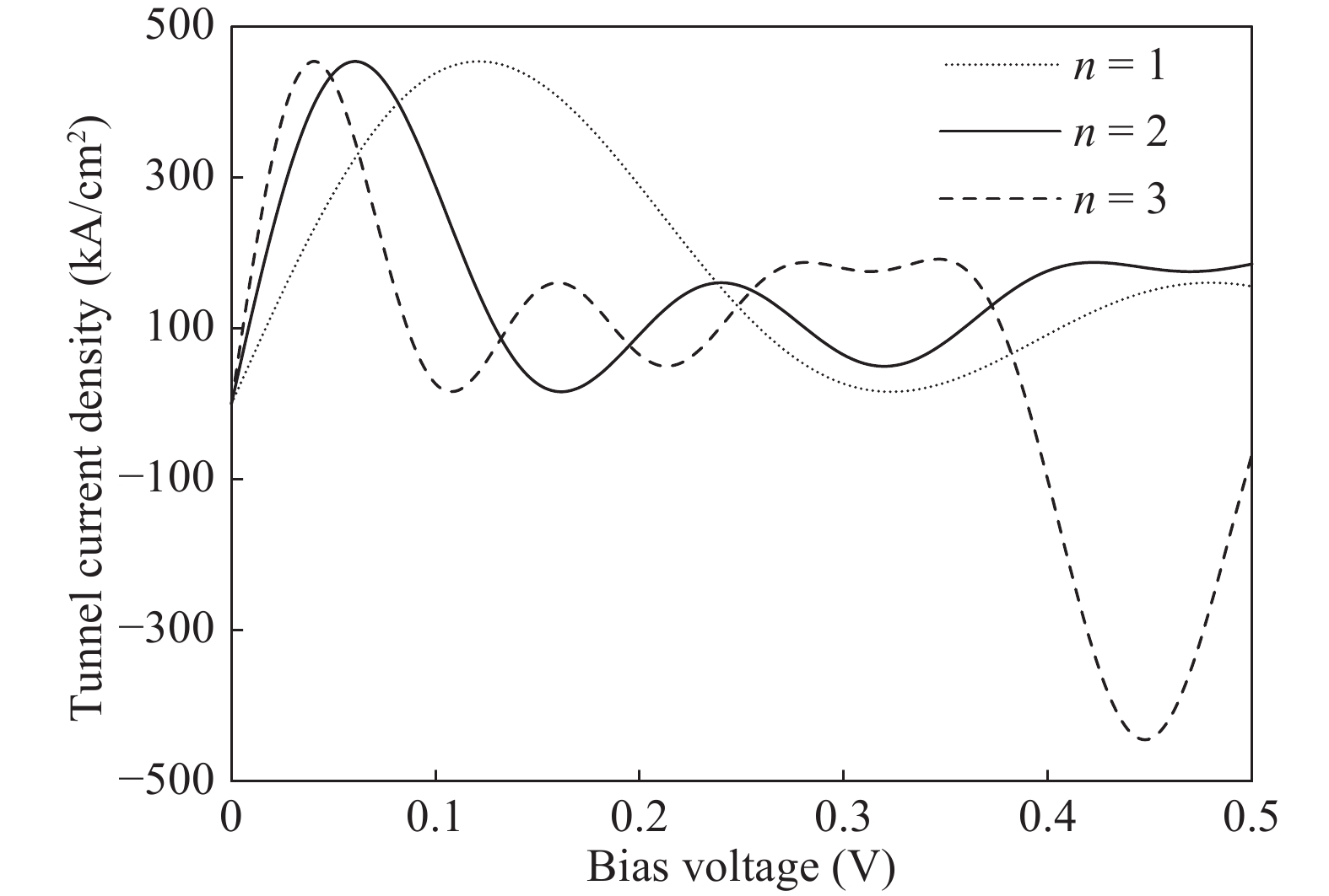
The double barrier quantum well (DBQW) resonant tunneling diode (RTD) structure made of SiGeSn/GeC/SiGeSn alloys grown on Ge substrate is analyzed. The tensile strained Ge1−zCz on Si1−x−yGexSny heterostructure provides a direct band gap type I configuration. The transmission coefficient and tunneling current density have been calculated considering single and multiple quantum wells. A comparative study of tunnelling current of the proposed structure is done with the existing RTD structure based on GeSn/SiGeSn DBH. A higher value of the current density for the proposed structure has been obtained.

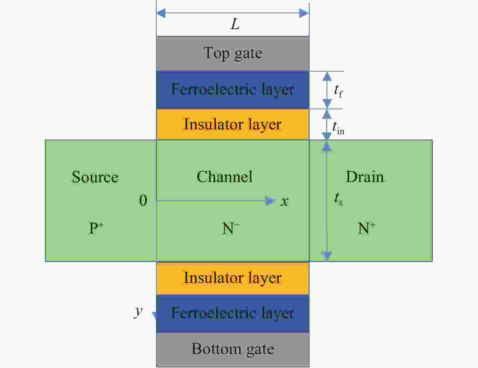
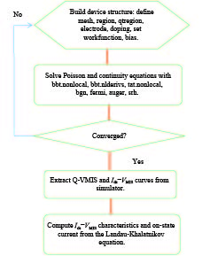
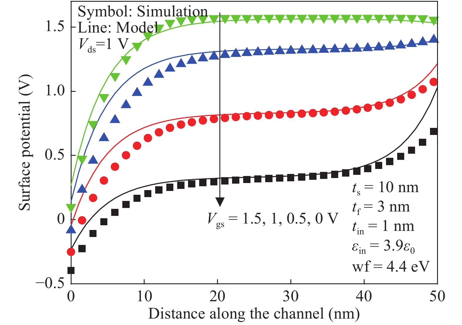
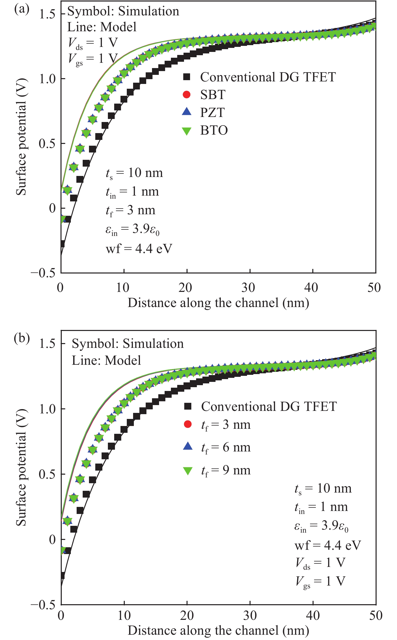
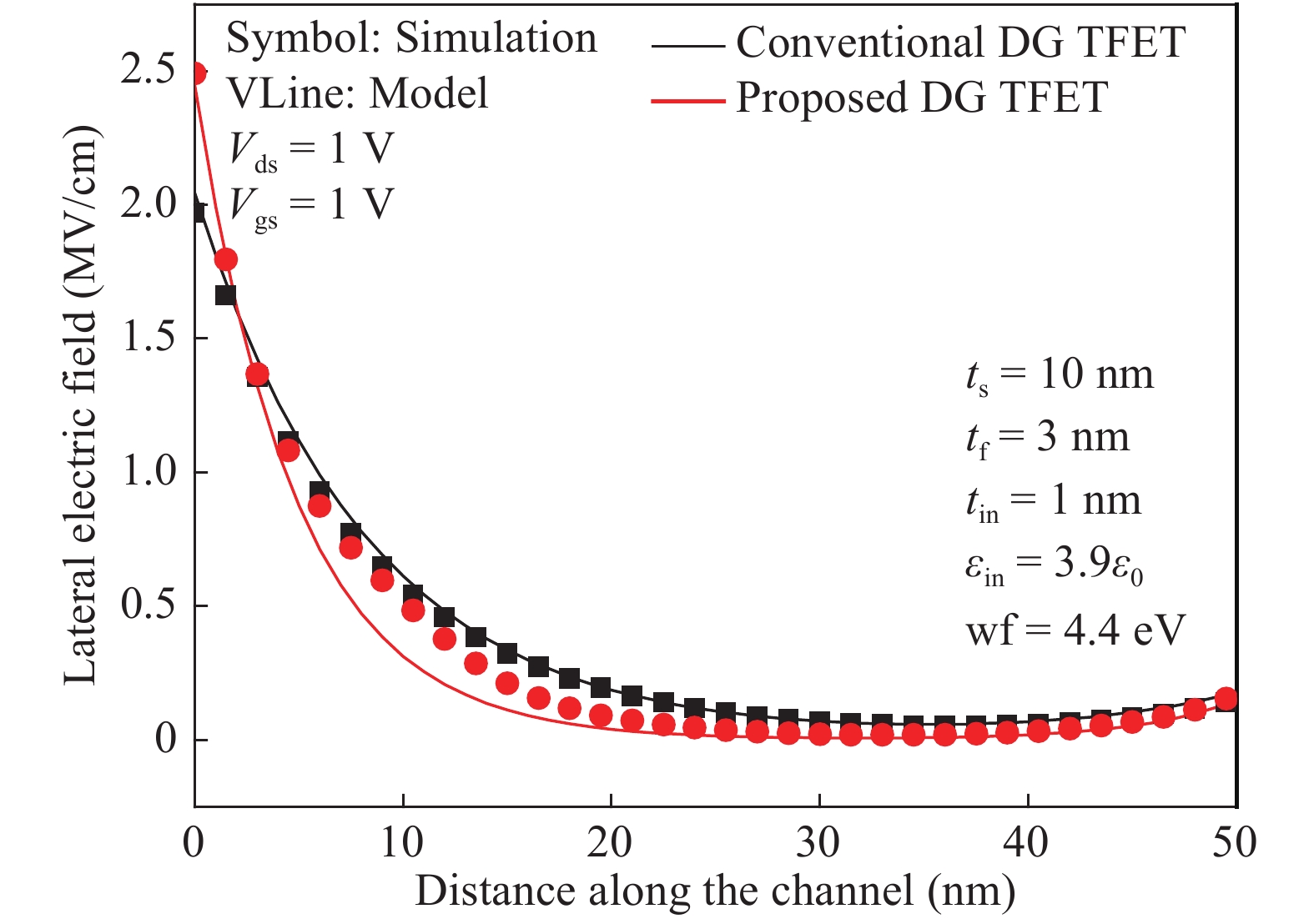
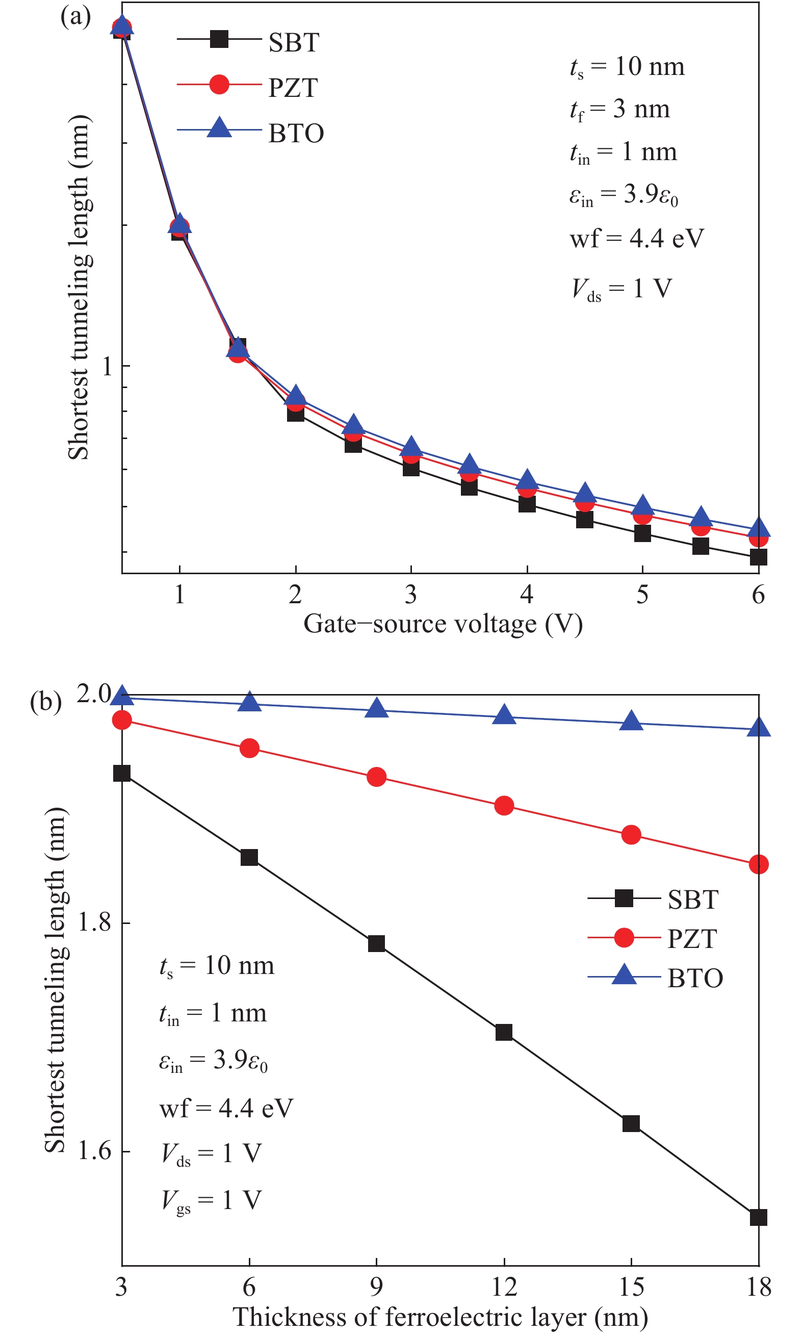
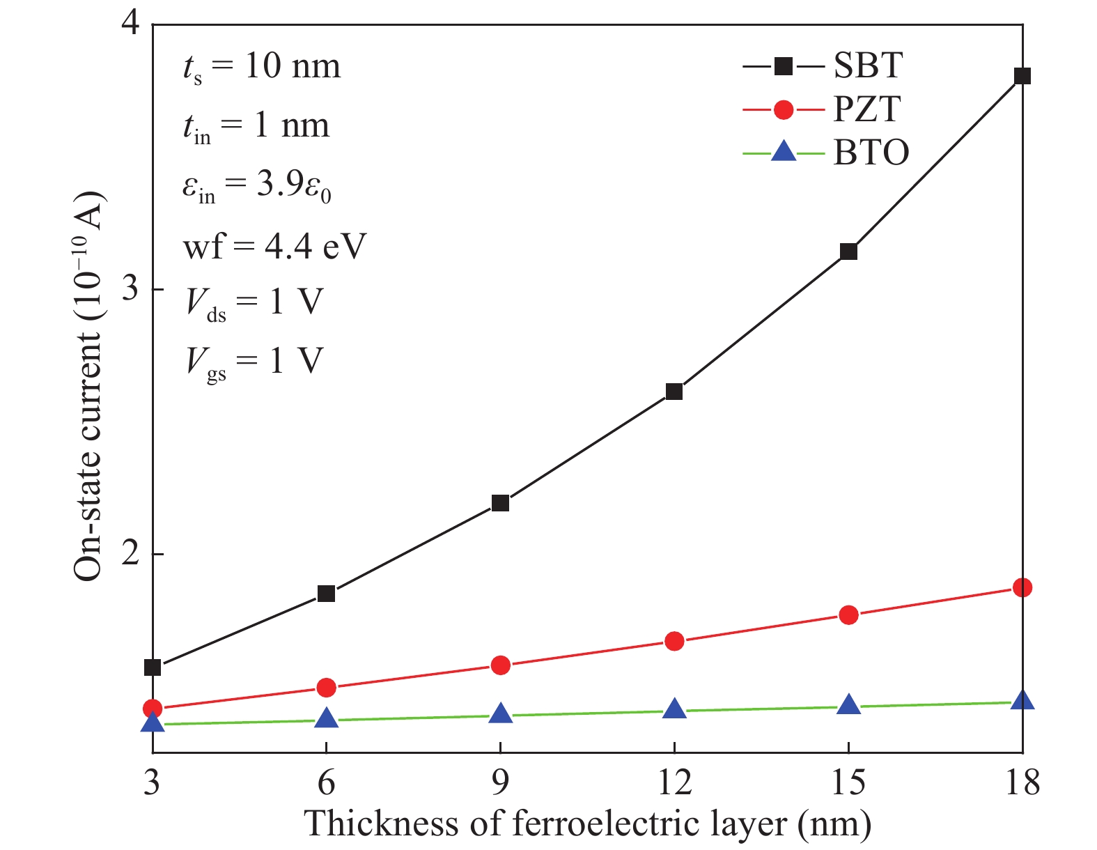
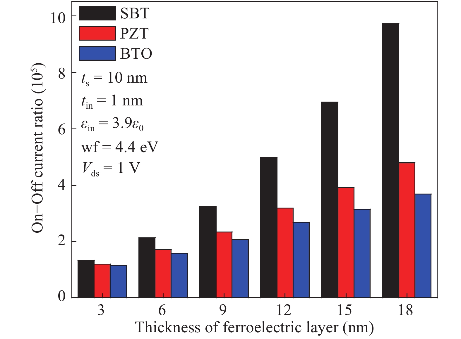
Analytical models are presented for a negative capacitance double-gate tunnel field-effect transistor (NC DG TFET) with a ferroelectric gate dielectric in this paper. The model accurately calculates the channel potential profile by solving the Poisson equation with the Landau–Khalatnikov (LK) equation. Moreover, the effects of the channel mobile charges on the potential are also taken into account. We also analyze the dependences of the channel potential and the on-state current on the device parameters by changing the thickness of ferroelectric layer, ferroelectric material and also verify the simulation results accord with commercial TCAD. The results show that the device can obtain better characteristics when the thickness of the ferroelectric layer is larger as it can reduce the shortest tunneling length.
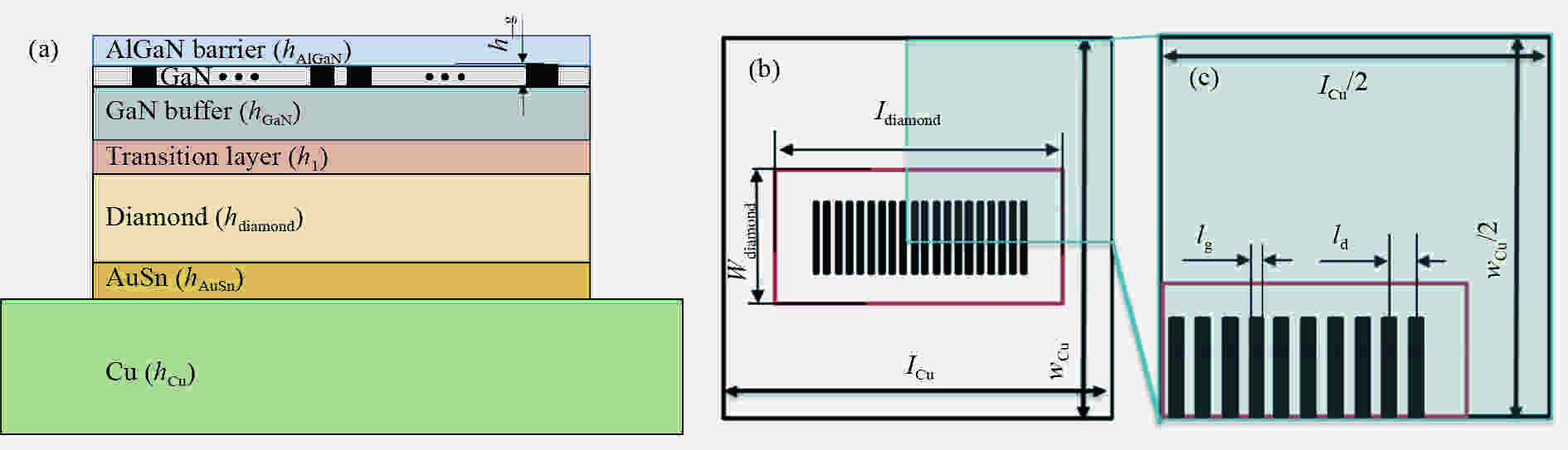
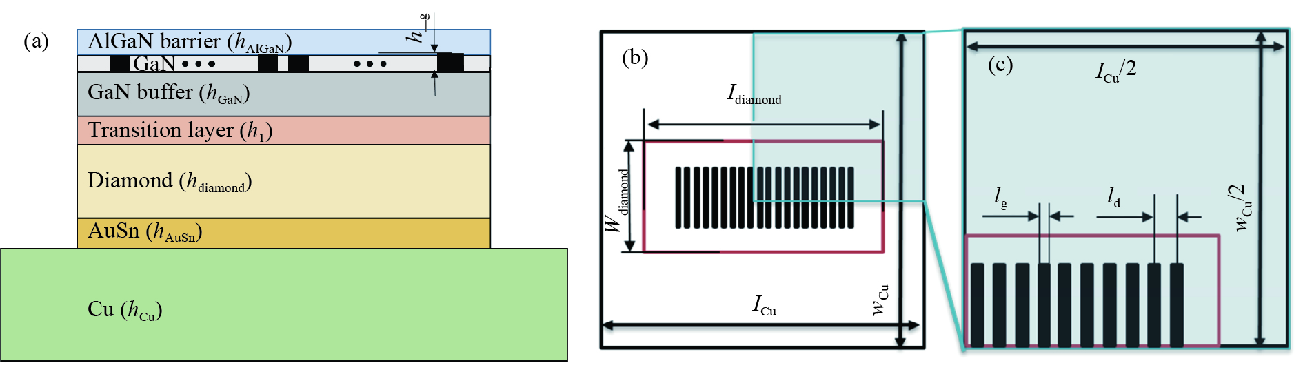
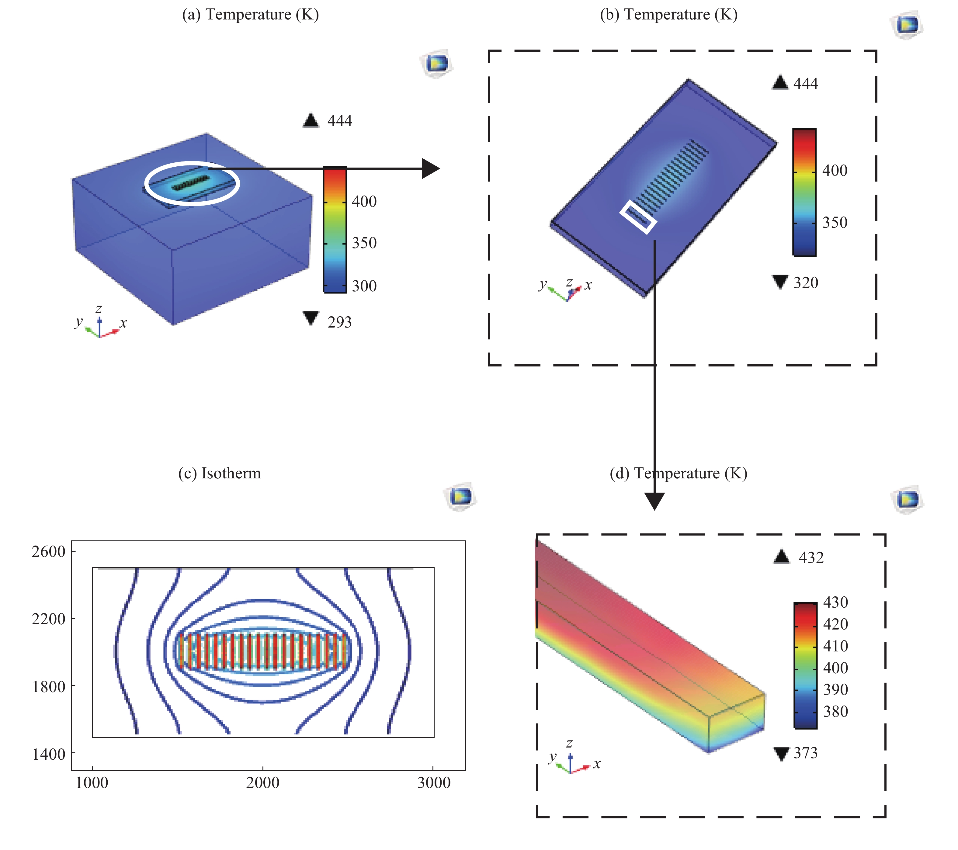
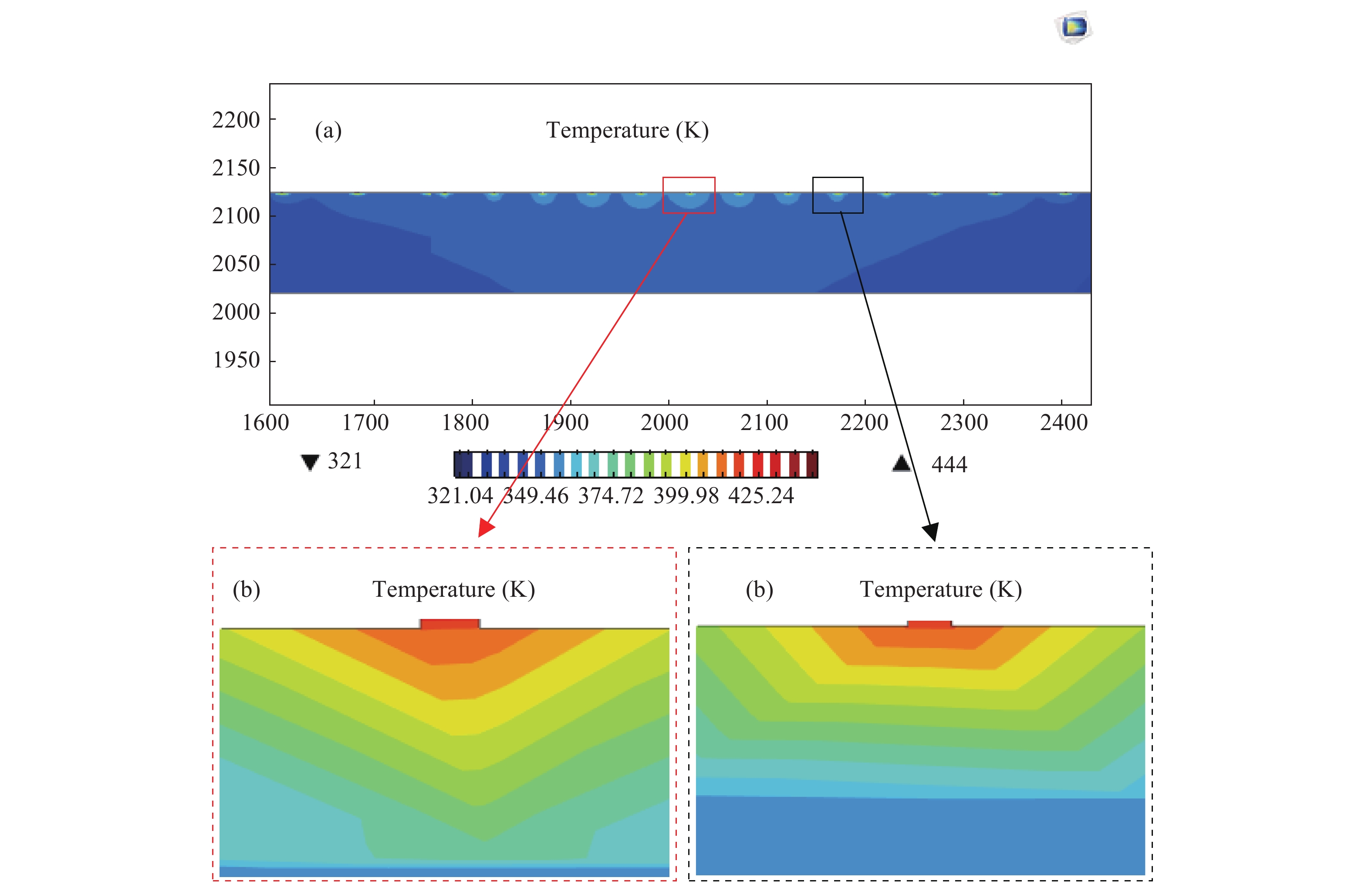
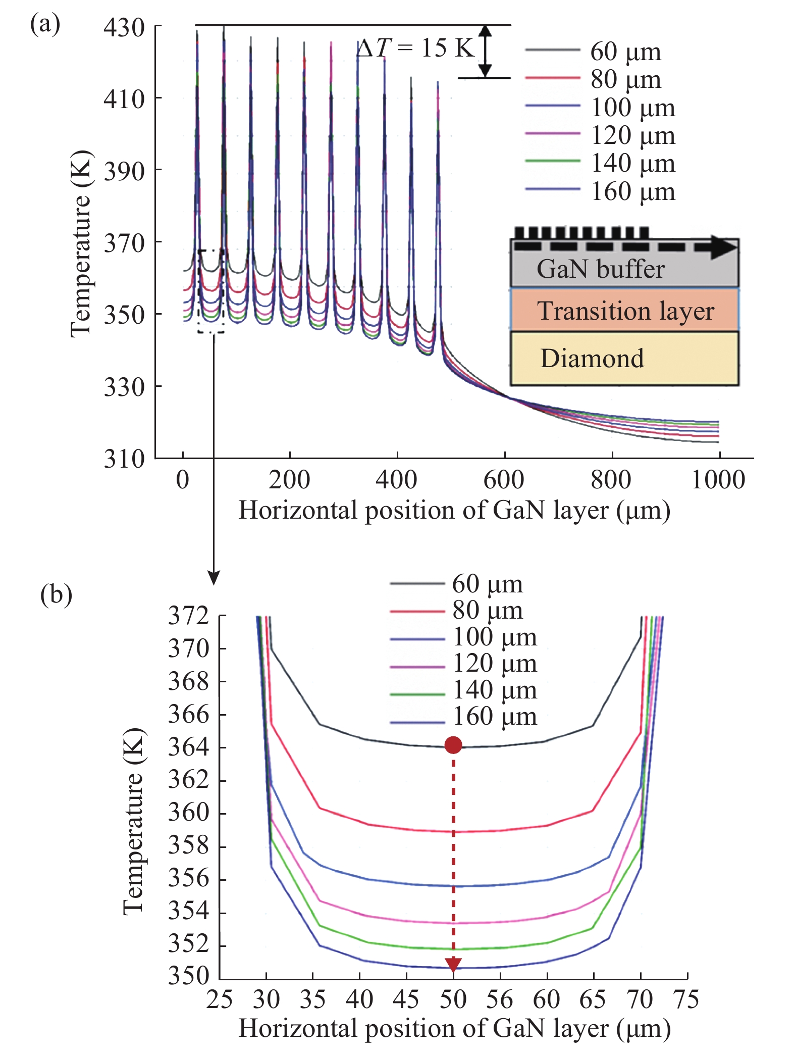
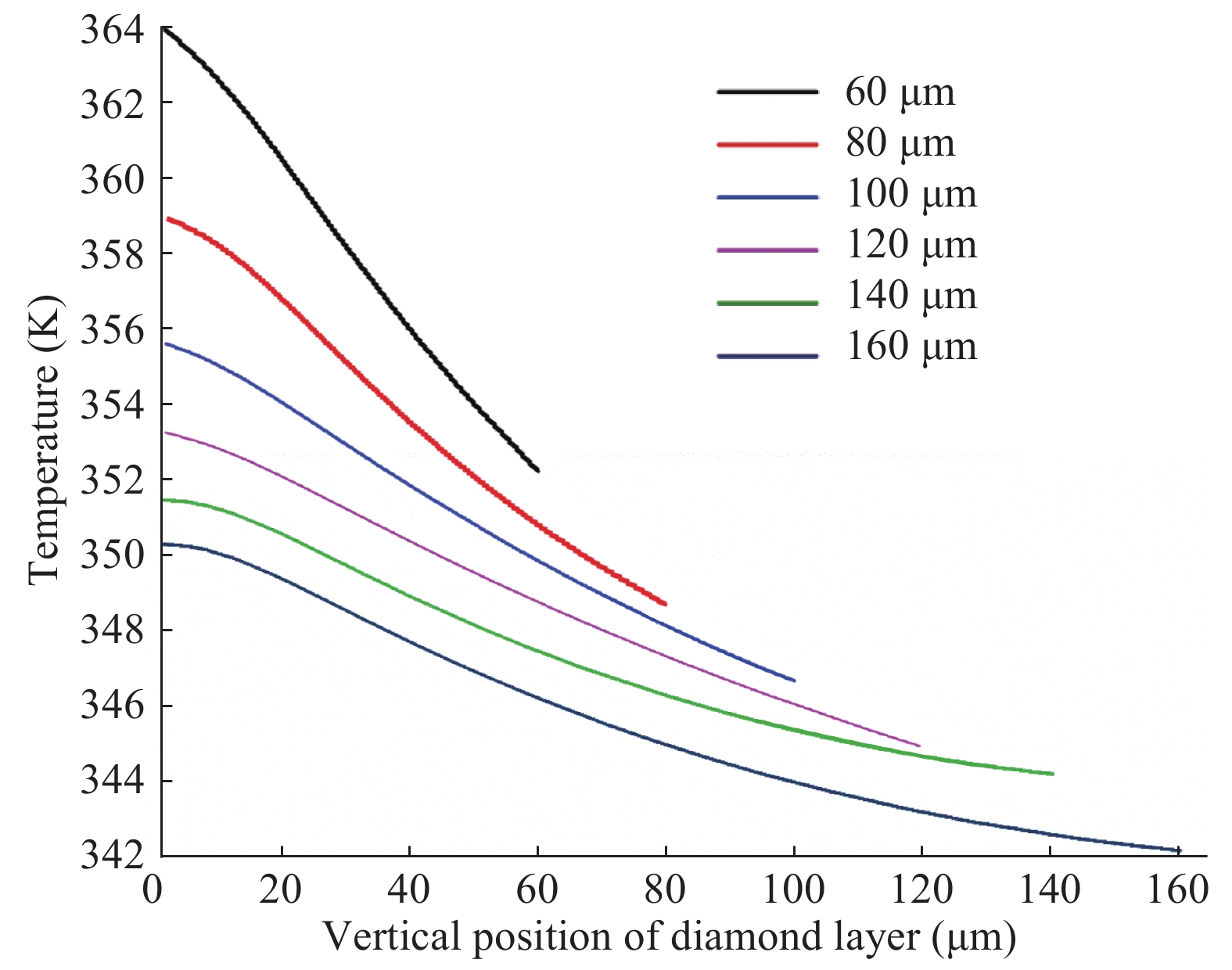
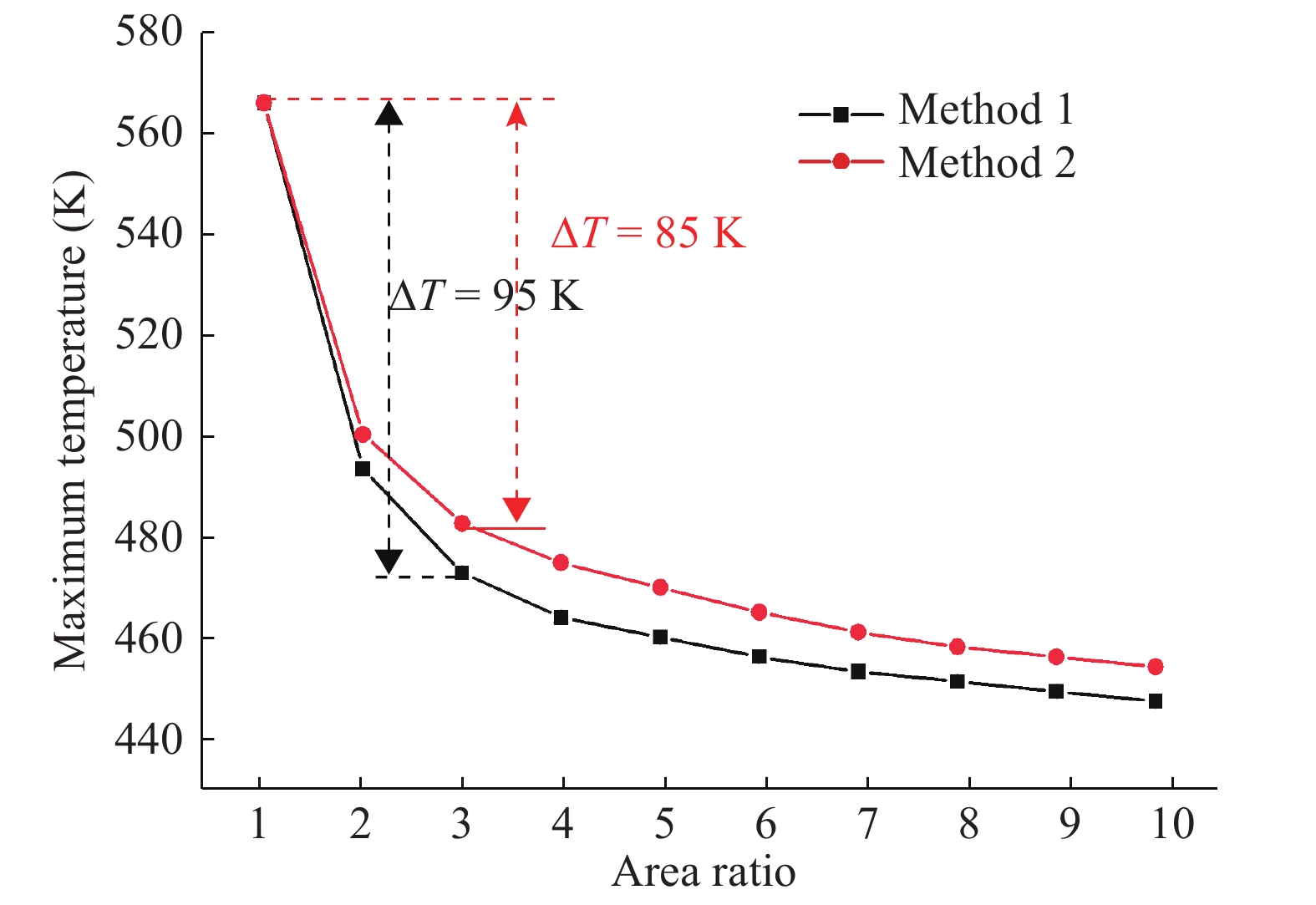
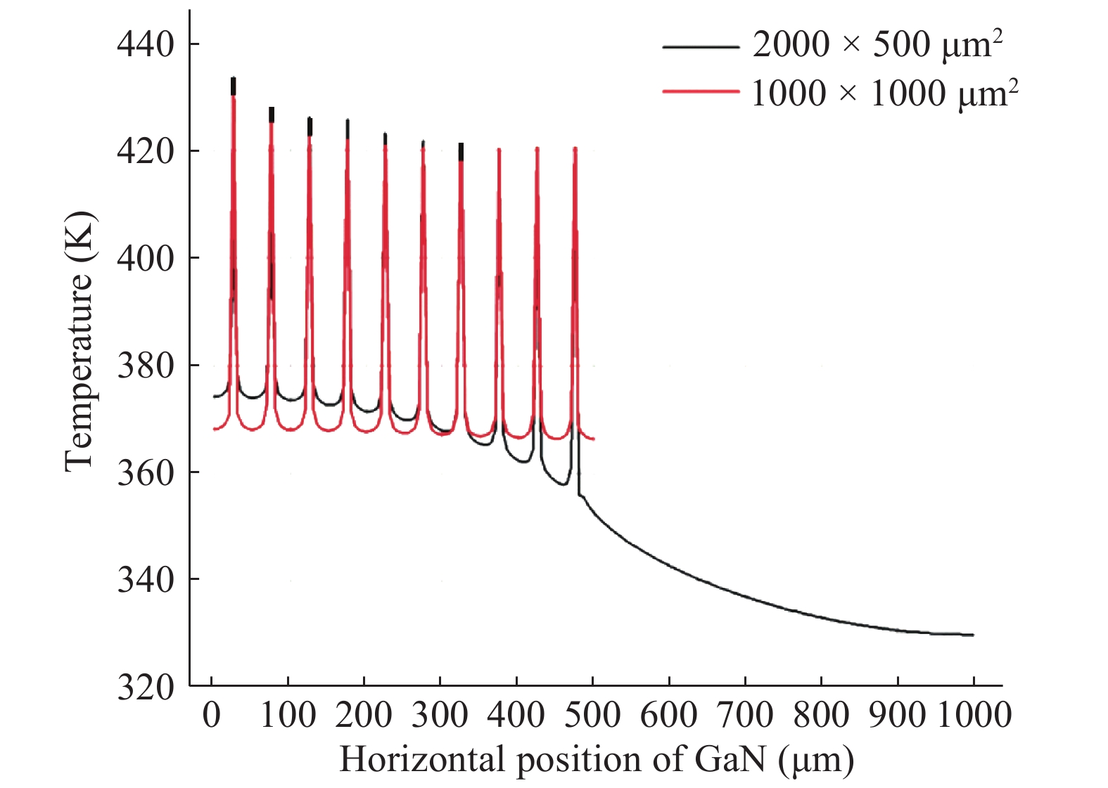
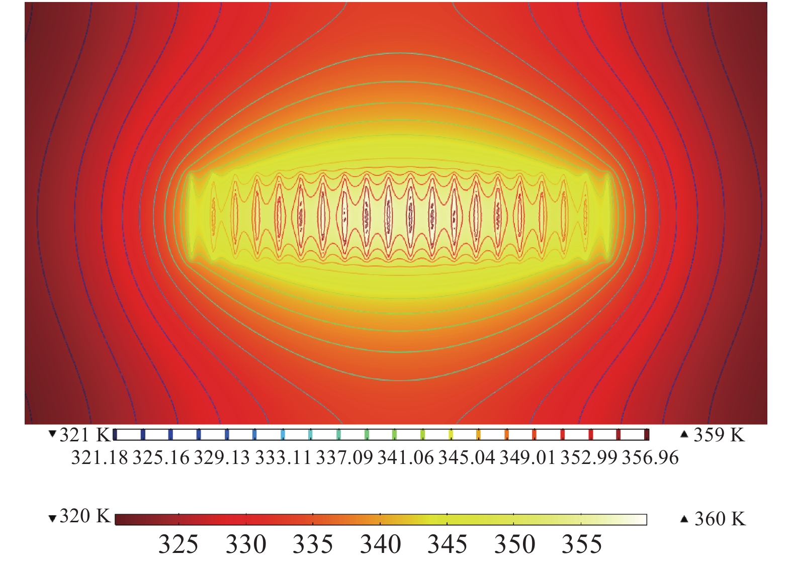
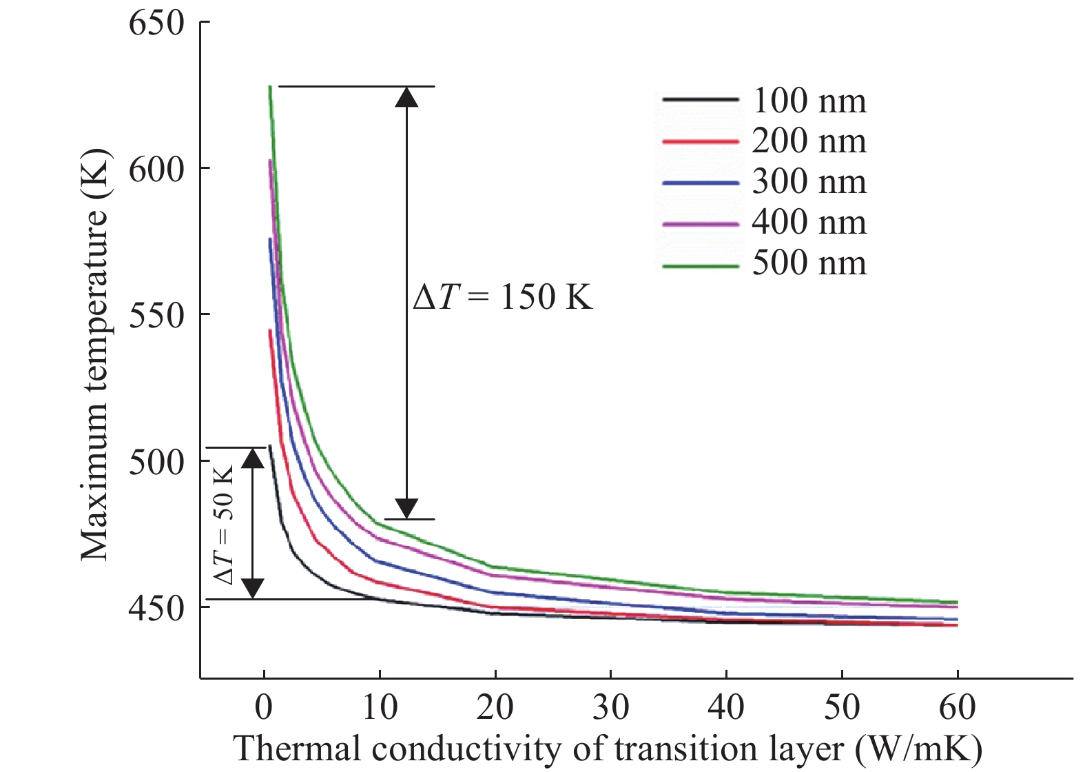
A three-dimensional thermal analysis of GaN HEMTs on diamond substrate is investigated using the finite element method. The diamond substrate thickness, area and shape, transition layer thickness and thermal conductivity of the transition layer are considered and treated appropriately in the numerical simulation. The temperature distribution and heat spreading paths are investigated under different conditions and the results indicate that the existence of the transition layer causes an increase in the channel temperature and the thickness, area and shape of the diamond substrate have certain impacts on the channel temperature too. Channel temperature reduces with increasing diamond substrate thickness and area but with a decreasing trend, which can be explained by the saturation effects of the diamond substrate. The shape of diamond substrate also affects the temperature performance of GaN HEMTs, therefore, to achieve a favorable heat dissipation effect with the settled diamond substrate area, the shape should contain as many isothermal curves as possible when the isothermal gradient is constant. The study of the thermal properties of GaN on diamond substrate is useful for the prediction of heating of high power GaN HEMTs devices and optimal designs of an efficient heat spreader for GaN HEMTs.

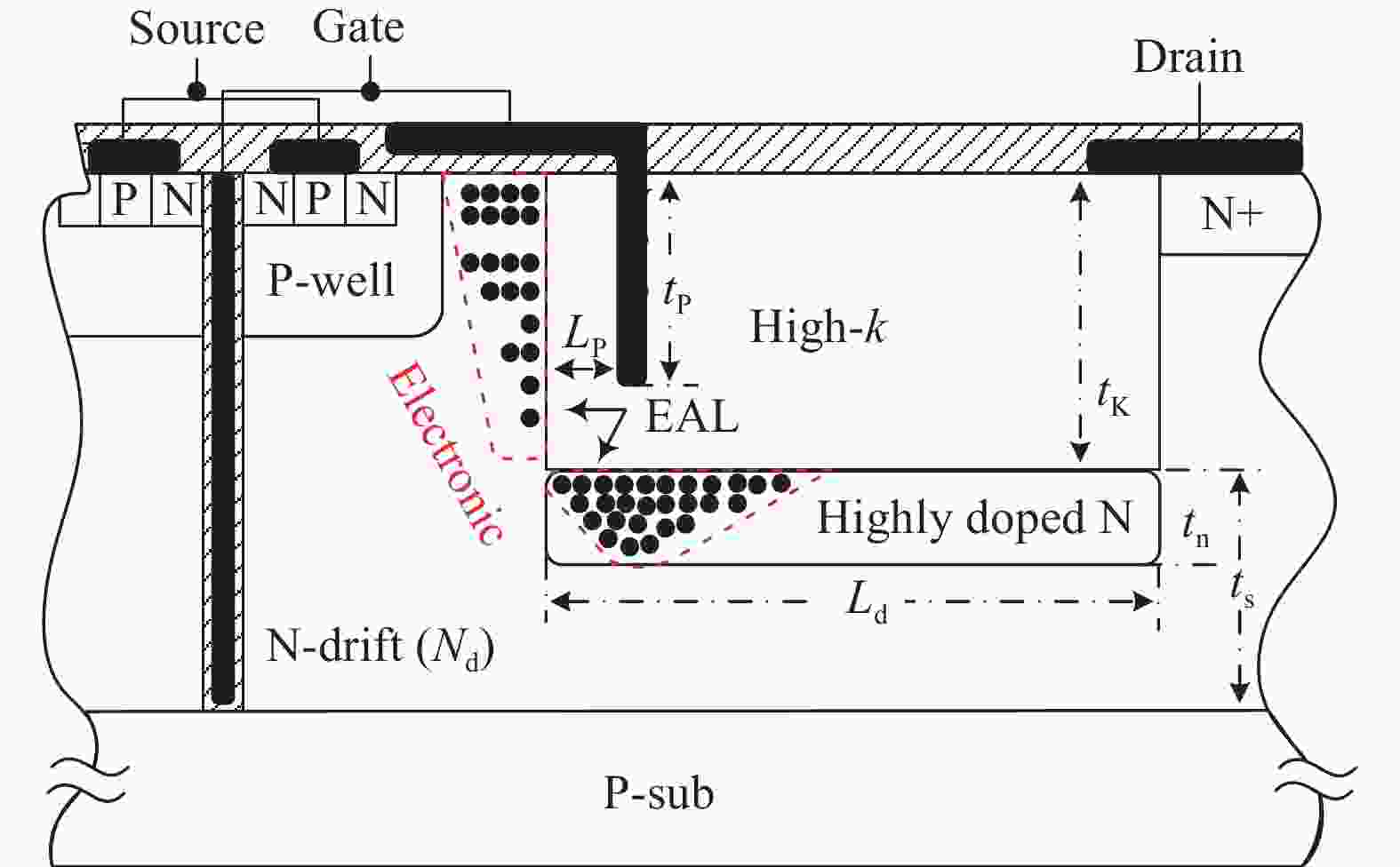
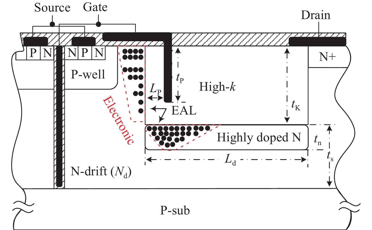
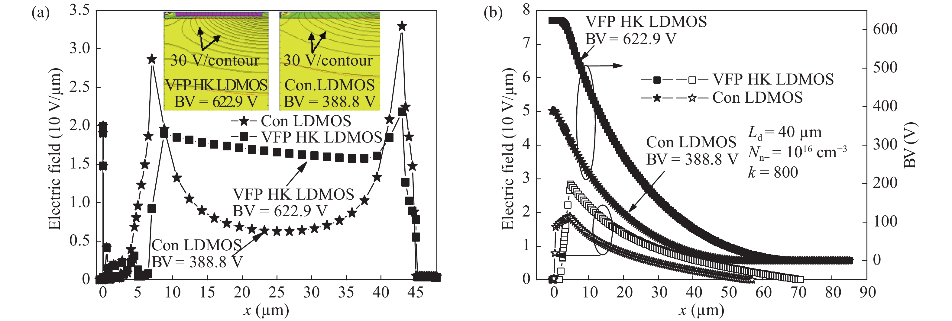
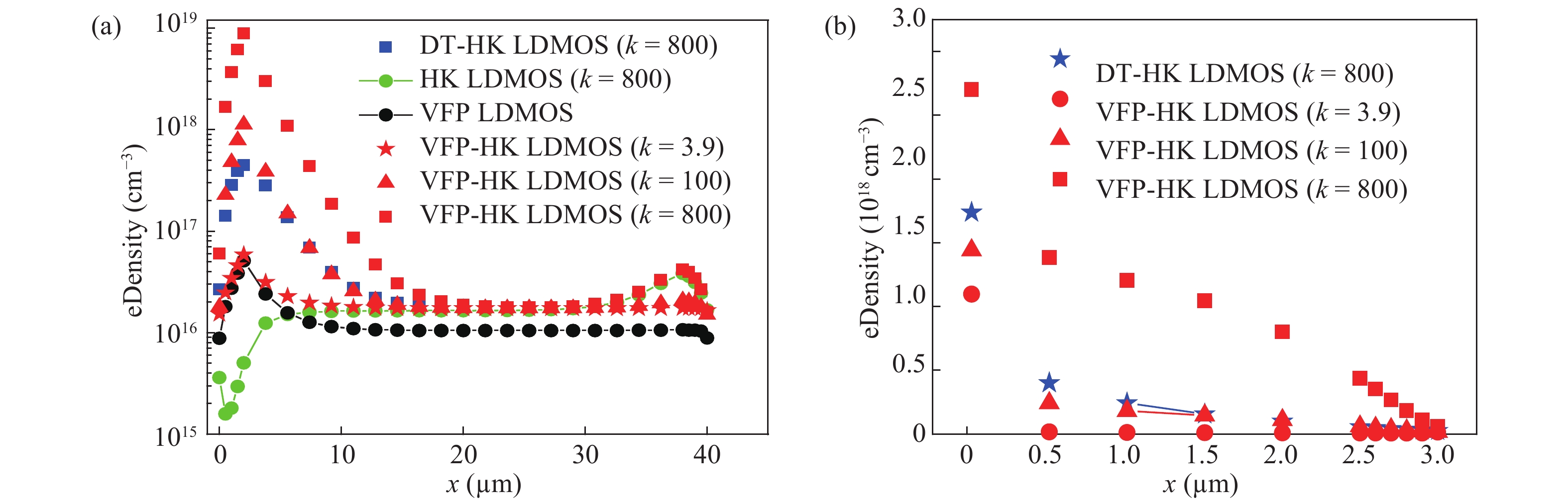
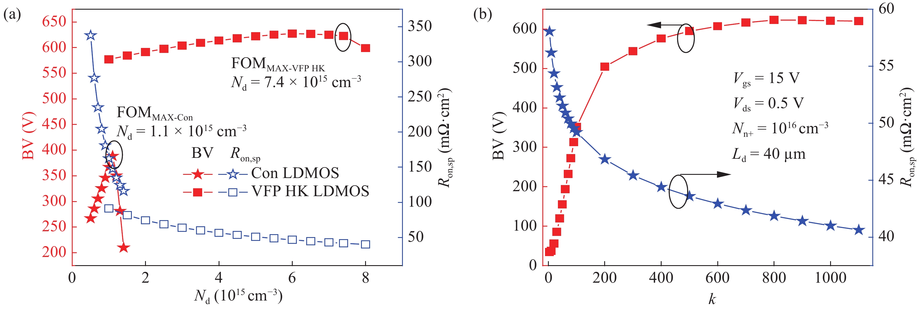
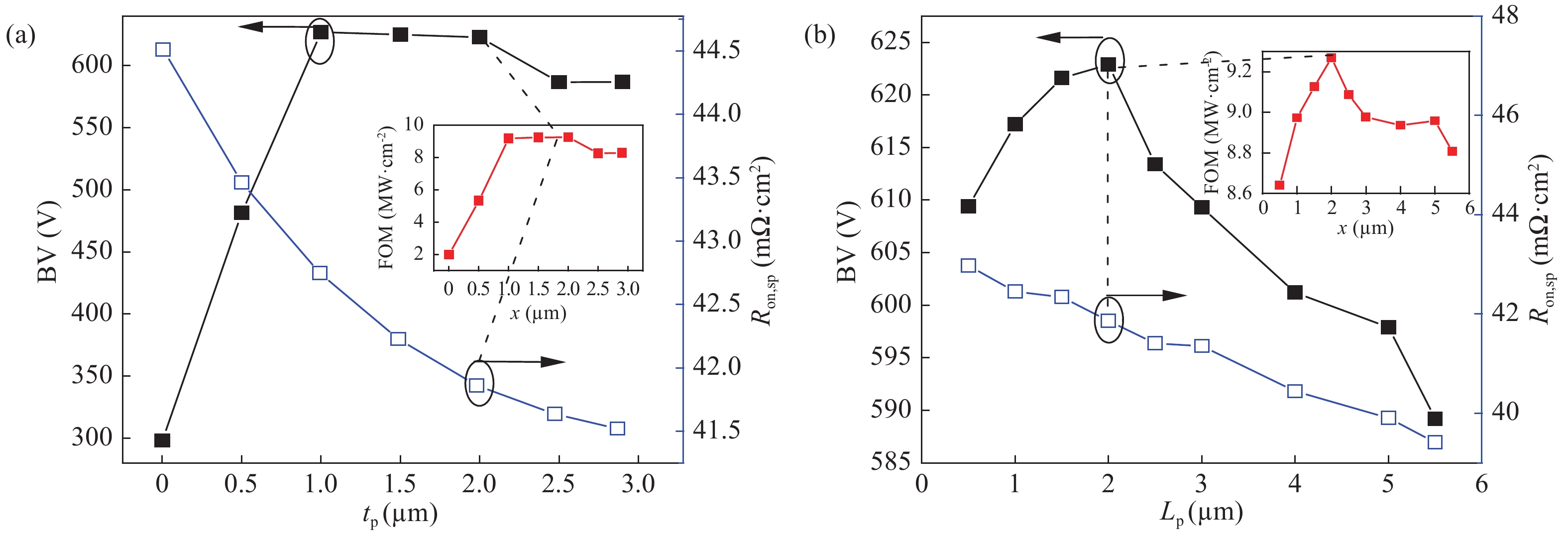
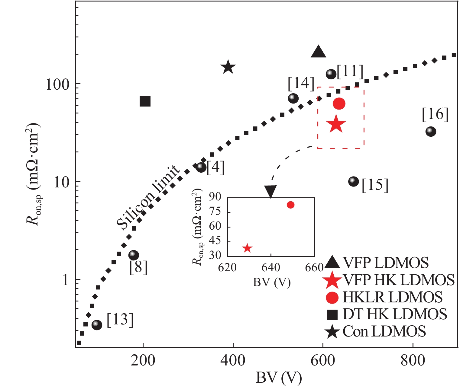
An ultralow specific on-resistance high-k LDMOS with vertical field plate (VFP HK LDMOS) is proposed. The high-k dielectric trench and highly doped interface N+ layer are made in bulk silicon to reduce the surface field of the drift region in the VFP HK LDMOS. The gate vertical field plate (VFP) pinning in the high-k dielectric trench can modulate the bulk electric field. The high-k dielectric not only provides polarized charges to assist depletion of the drift region, so that the drift region and high-k trench maintain charge balance adaptively, but also can fully assist in depleting the drift region to increase the drift doping concentration and reshape the electric field to avoid premature breakdown. Compared with the conventional structure, the VFP HK LDMOS has the breakdown voltage of 629.1 V at the drift length of 40 μm and the specific on-resistance of 38.4 mΩ·cm2 at the gate potential of 15 V. Then the power figure of merit is 10.31 MW/cm2.


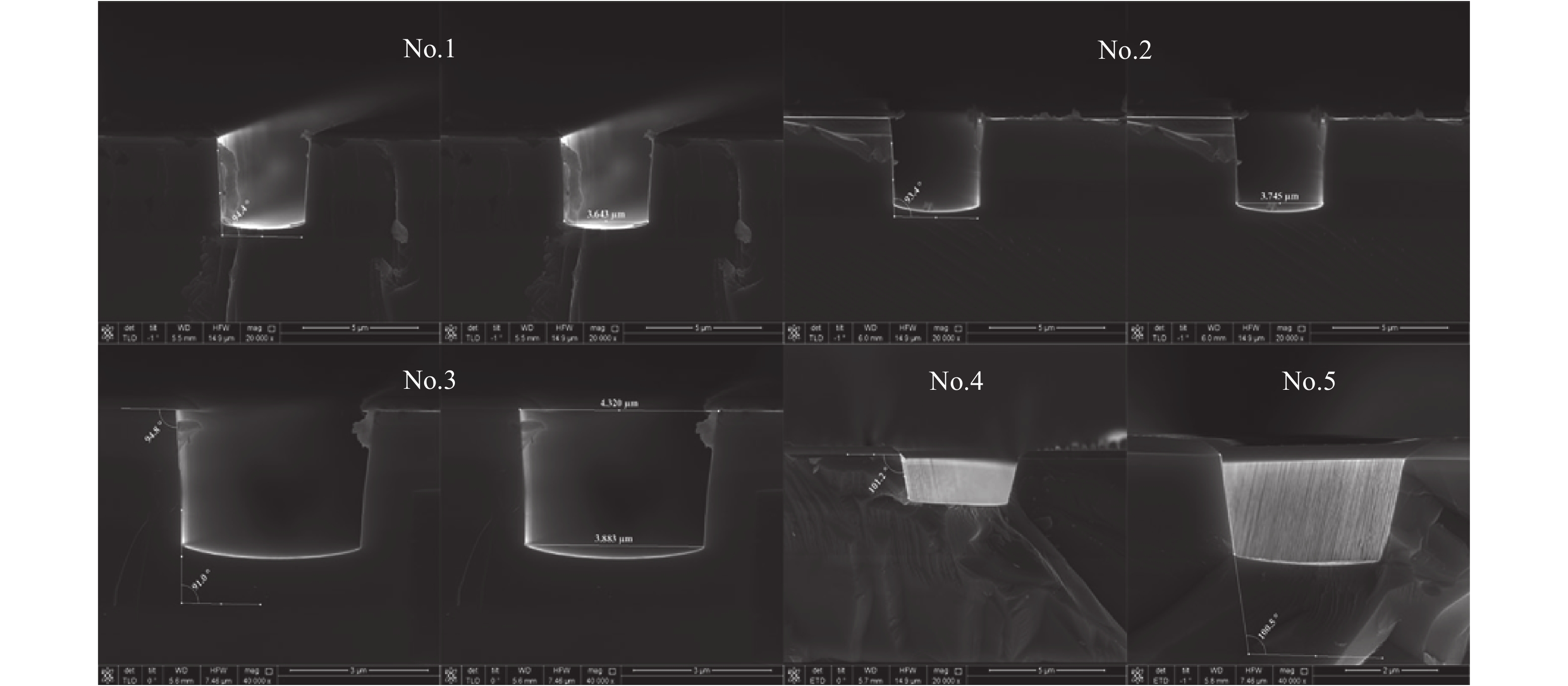
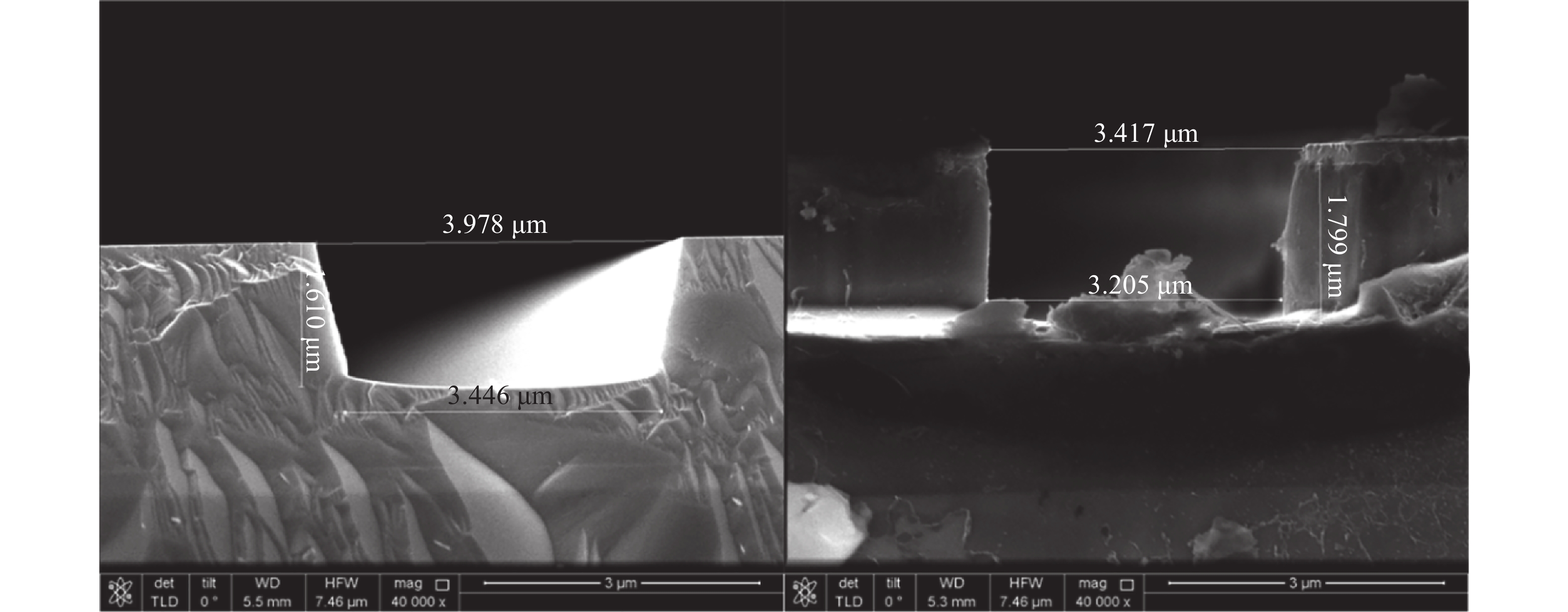
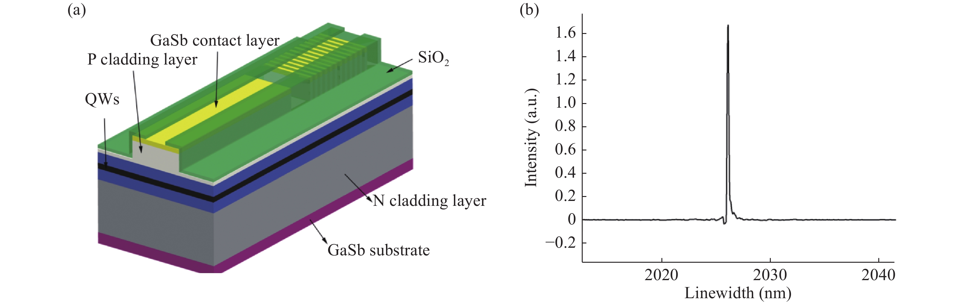
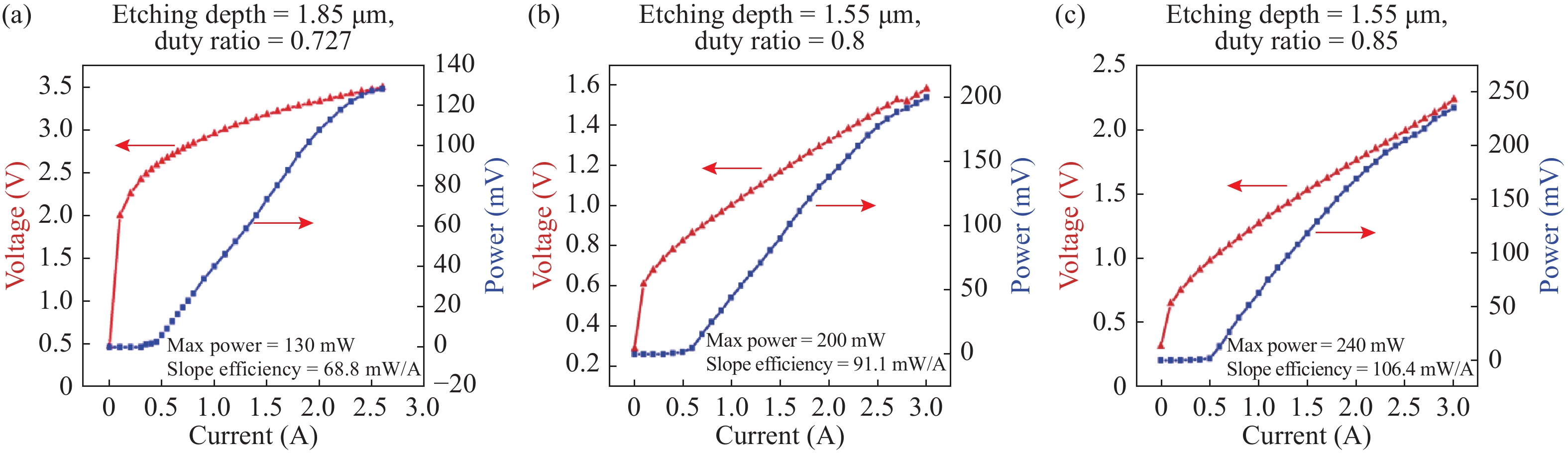
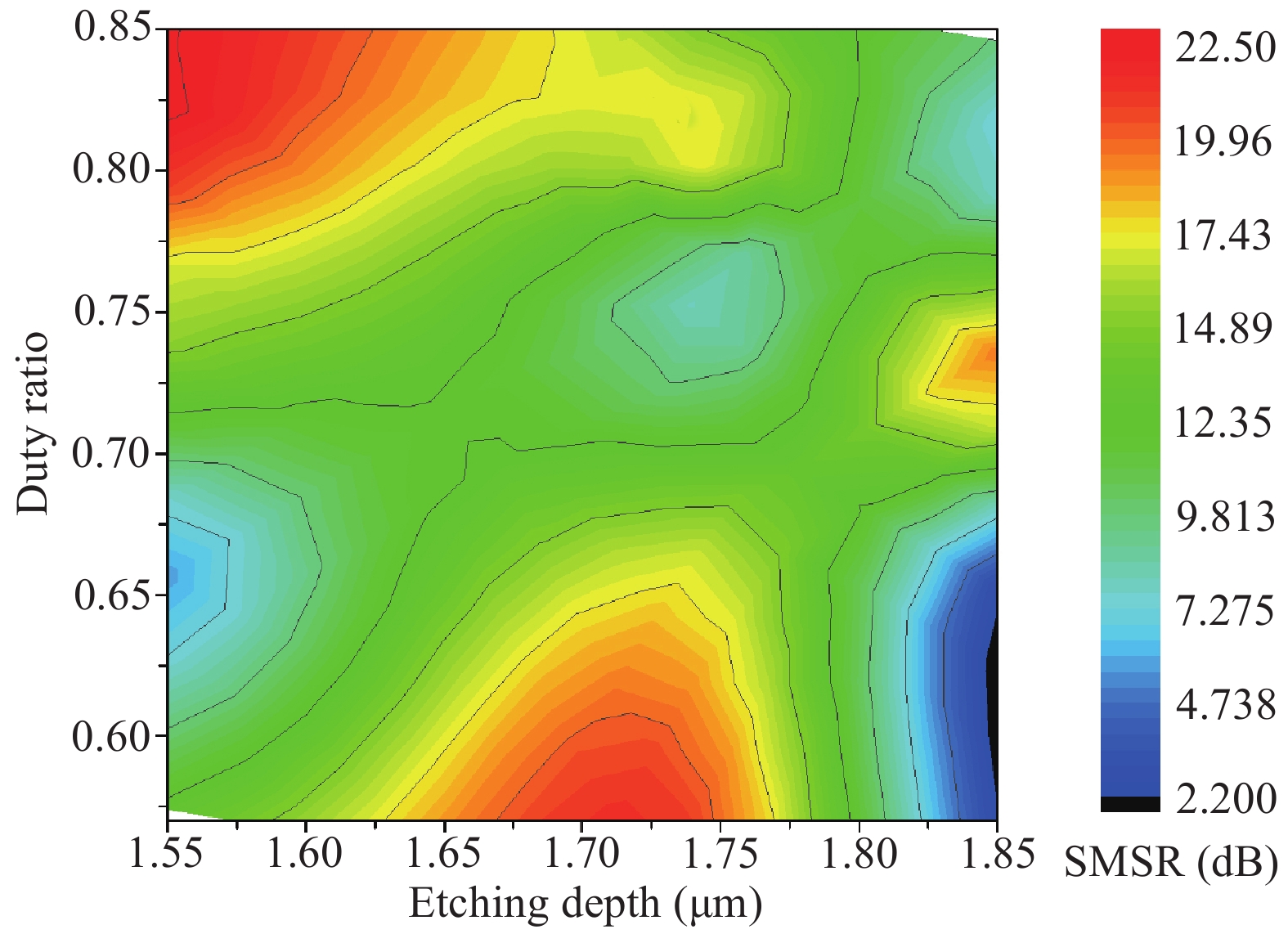
The GaSb-based distributed Bragg reflection (DBR) diode laser with 23rd-order gratings have been fabricated by conventional UV lithography and inductively coupled plasma (ICP) etching. The ICP etching conditions were optimized and the relationship among etching depth, duty ratio and side-mode suppression ratio (SMSR) was studied. The device with a ridge width of 100 μm, gratings period of 13 μm and etching depth of 1.55 μm as well as the duty ratio of 85% was fabricated, its maximum SMSR reached 22.52 dB with uncoated cavity facets under single longitudinal operation mode at room temperature.


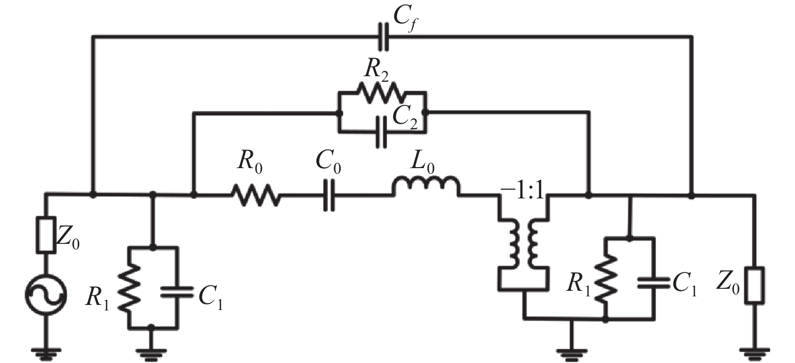
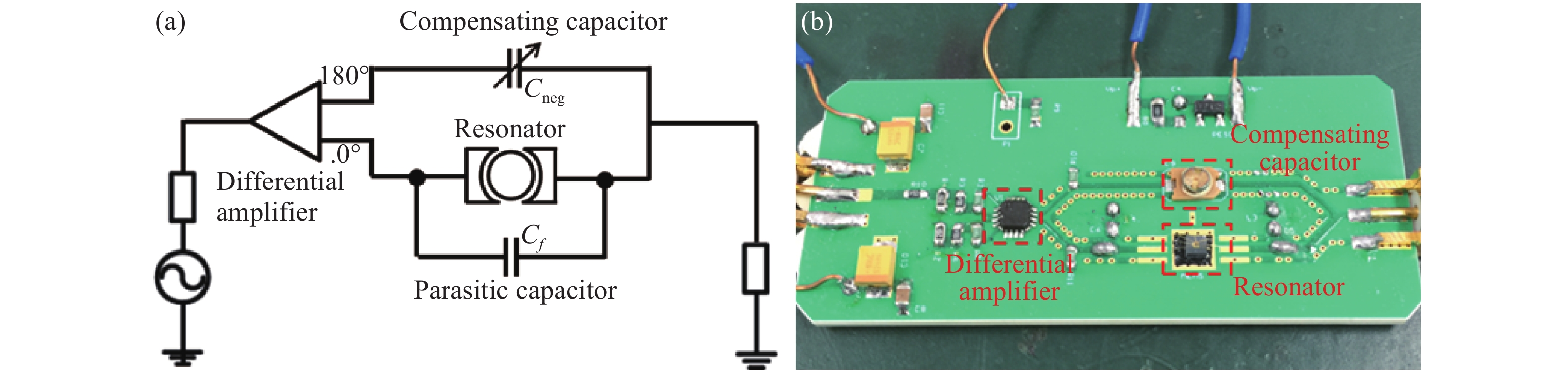
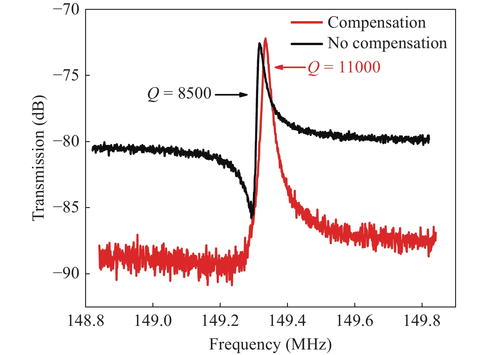
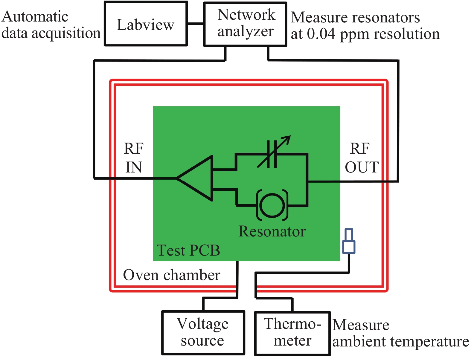
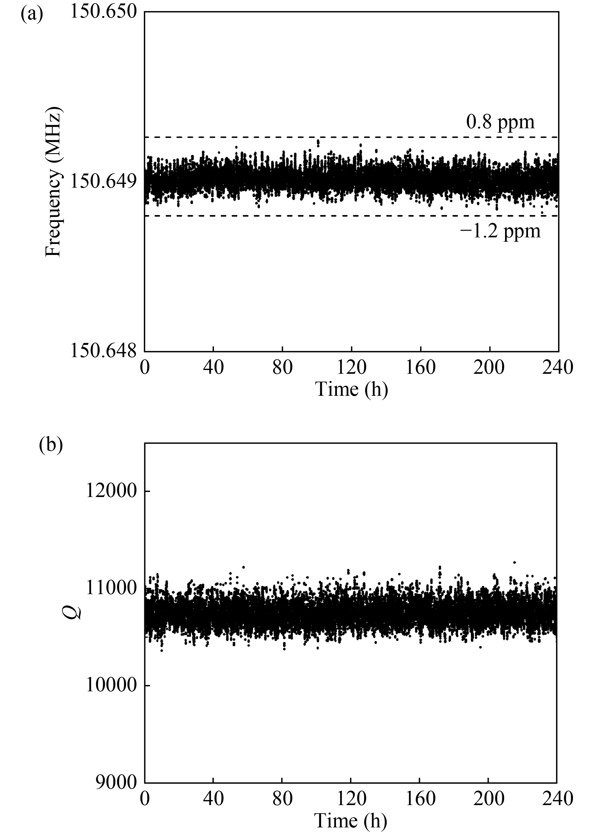
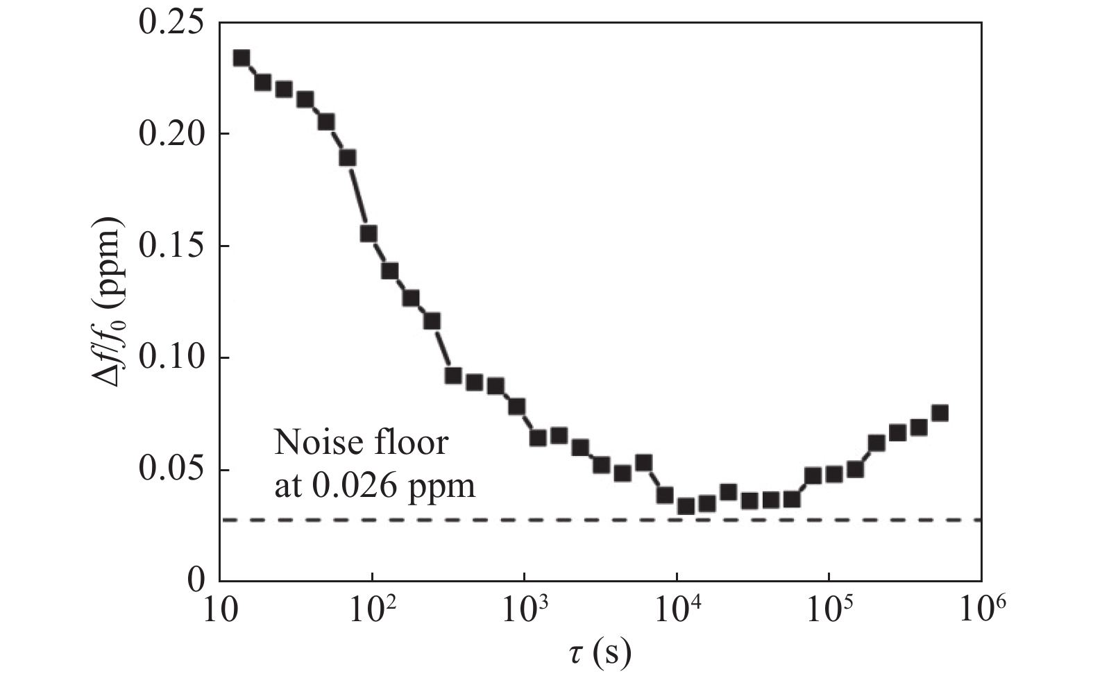
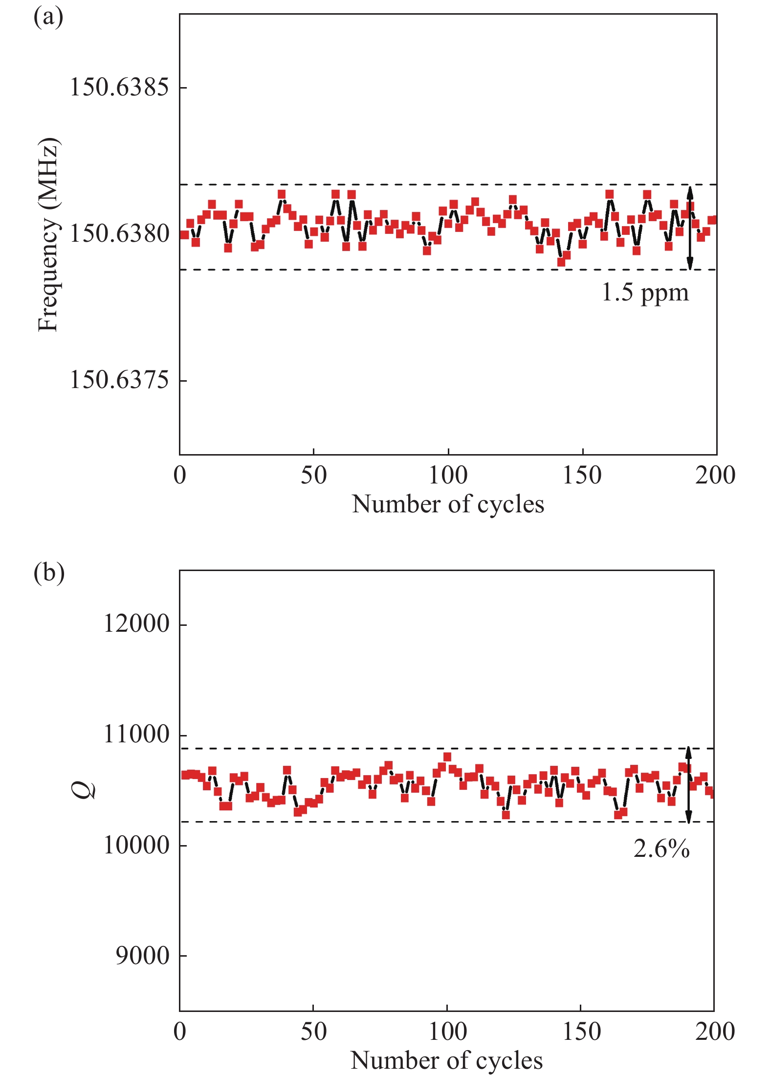
The frequency stability of a three-dimensional (3D) vacuum encapsulated very high frequency (VHF) disk resonator is systematically investigated. For eliminating the parasitic effect caused by the parasitic capacitance of the printed circuit board (PCB), a negating capacitive compensation method was developed. The testing results implemented at 25 °C for 240 h for the long-term stability indicates that the resonant frequency variation remained within ±1 ppm and the noise floor derived from Allan Deviation was 26 ppb, which is competitive with the conventional quartz resonators. The resonant frequency fluctuation of 1.5 ppm was obtained during 200 temperature cycling between −40 and 85 °C.

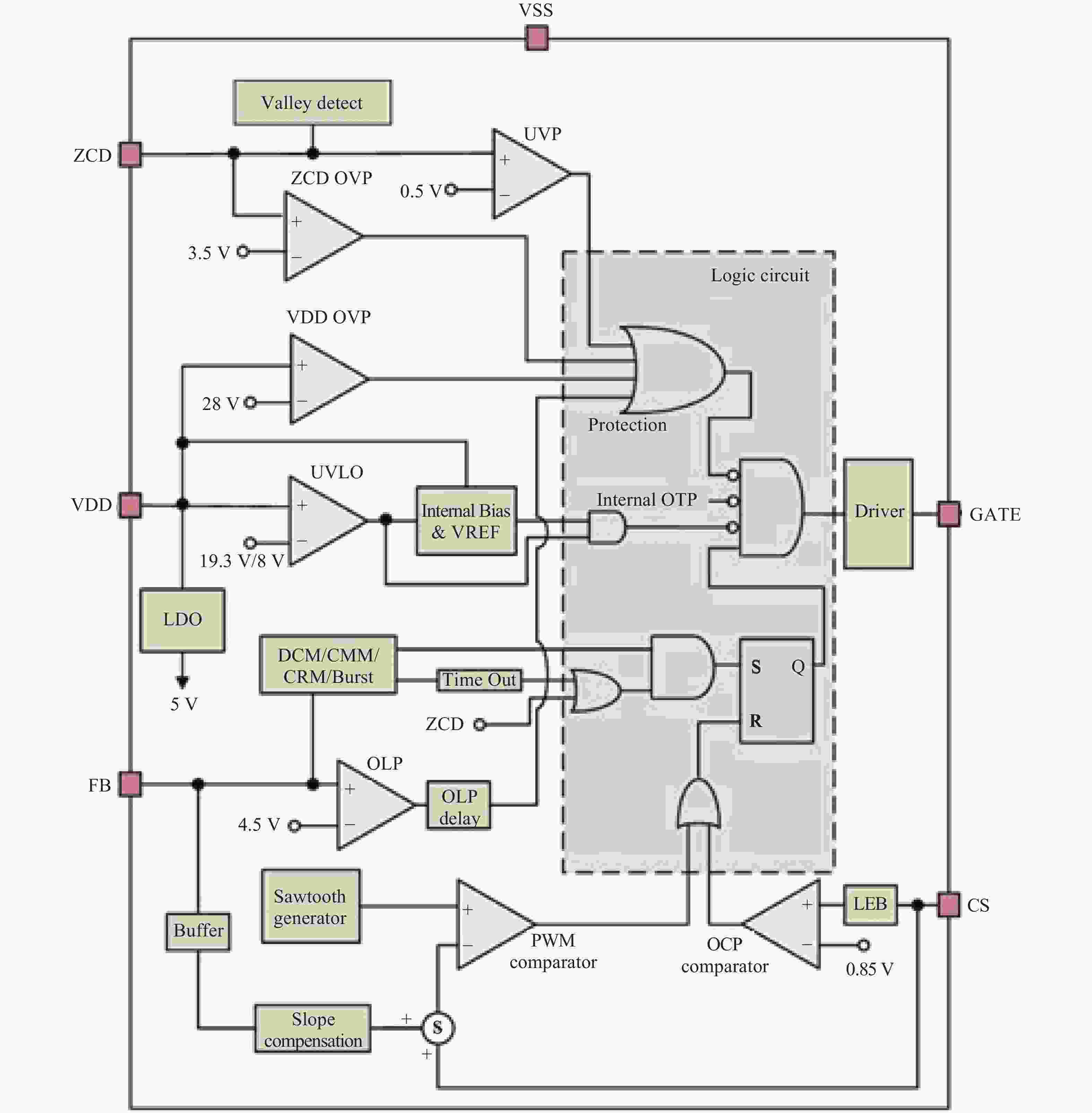
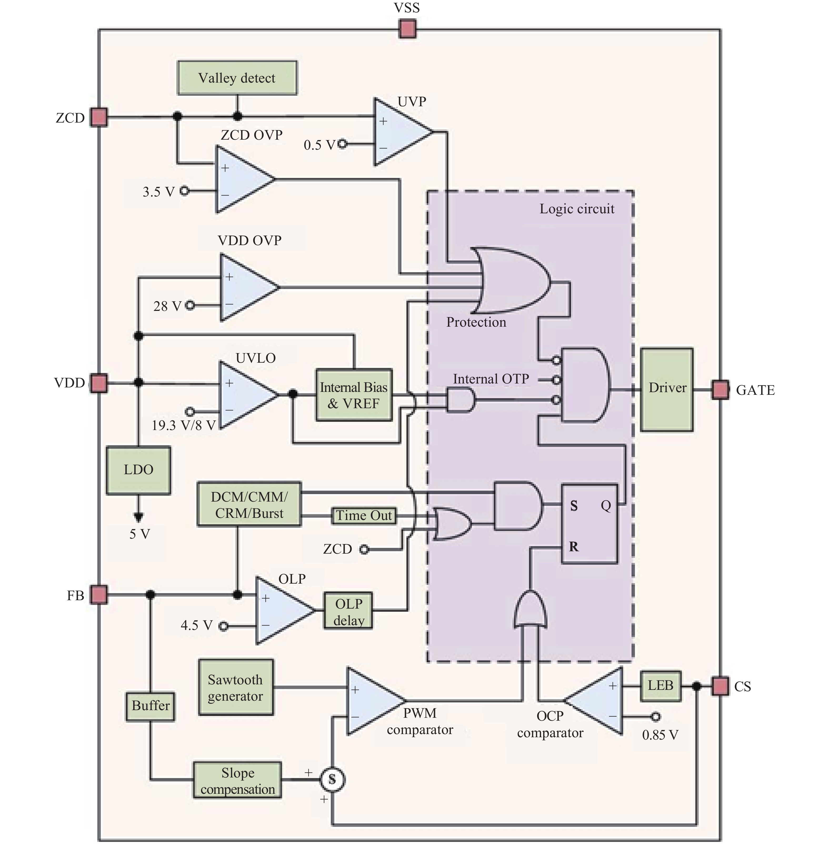
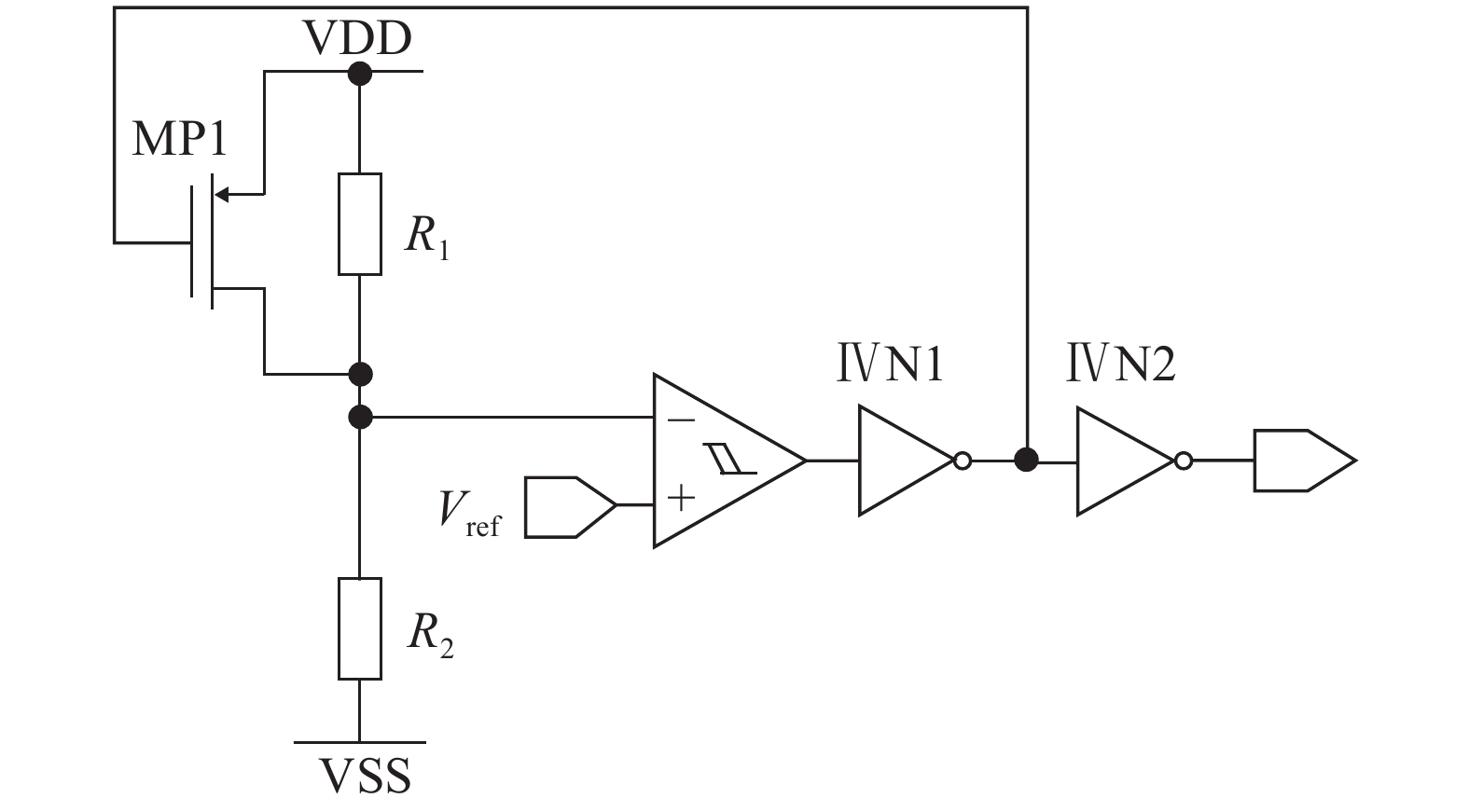
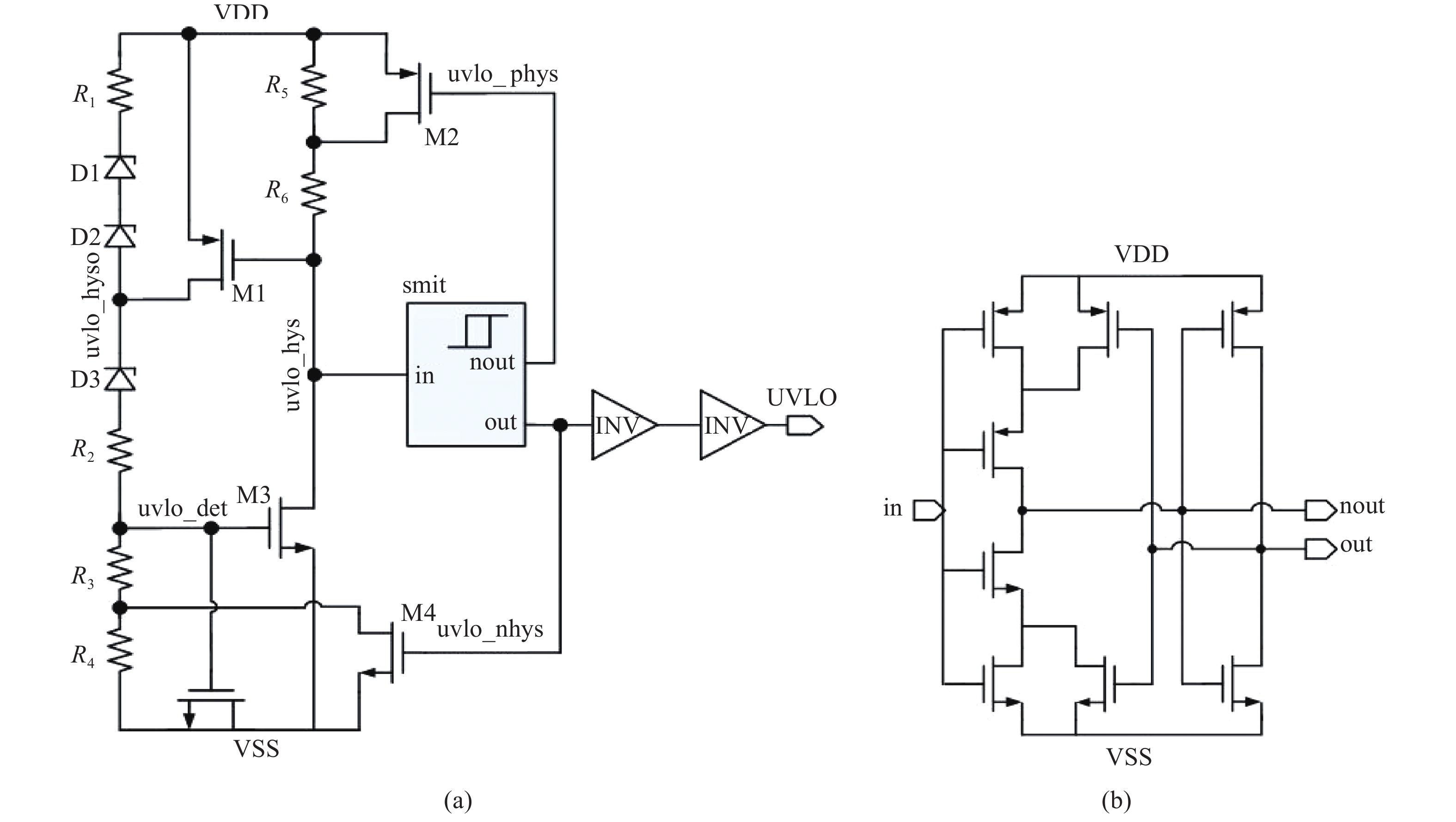
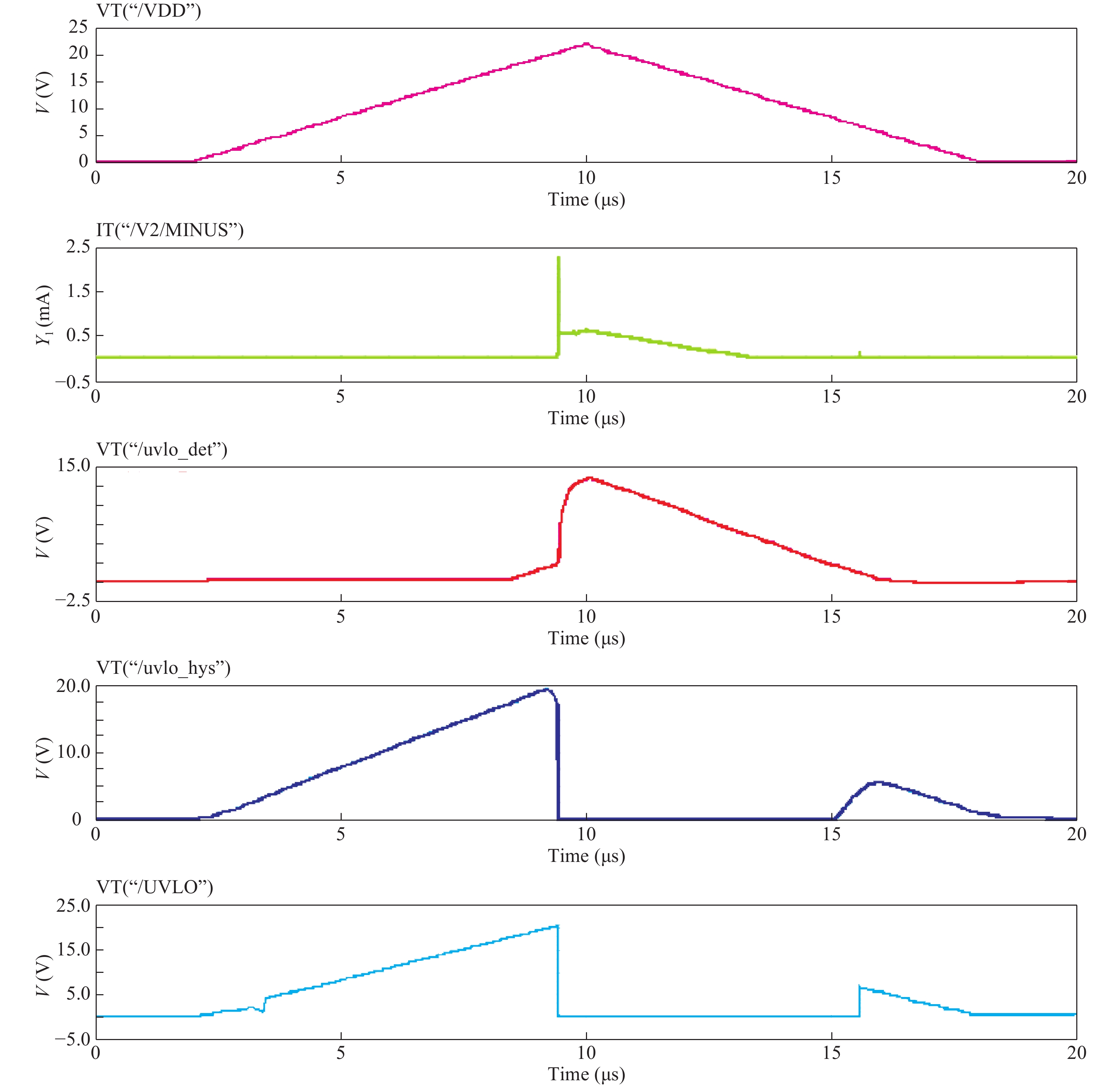
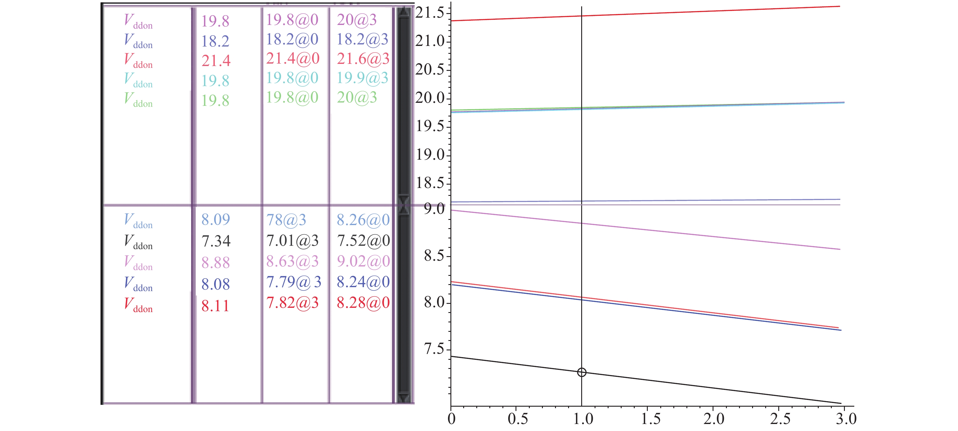
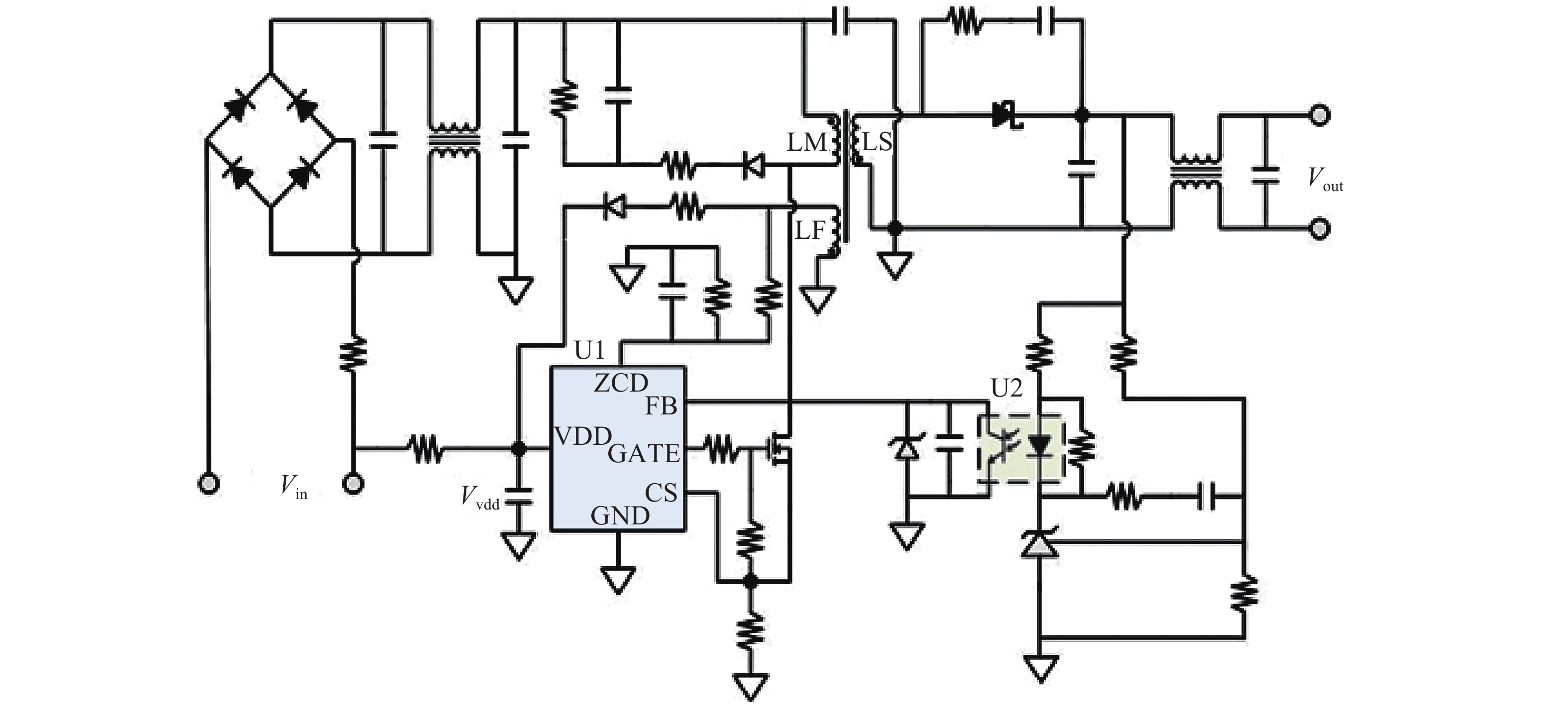
This paper proposes a high-performance pulse-width modulation (PWM) AC/DC controller, which can drive a high-voltage (HV) 650-V power metal-oxide-semiconductor field-effect Transistor (MOSFET) in typical applications of adapters in portable electronic devices. In order to reduce the standby power consumption and improve the response speed in the start-up state, an improved under voltage lockout (UVLO) circuit without a voltage reference source or comparator is adopted. The AC/DC controller is fabricated using a 40-V 0.8-μm one-poly two-metal (1P2M) CMOS process, and it only occupies 1410 × 730 μm2. A 12 V/2 A flyback topology for quick-charge application is illustrated as the test circuit, which is currently one of the most advanced power adapters in use. Test values show that the turn-on and the turn-off threshold voltages are 19.318 and 8.01 V, respectively. A high hysteresis voltage of 11.308 V causes the value of the power-charging capacitor to decrease to as low as 1 μF to reduce production cost. In addition, the start-up current of 2.3 μA is extremely small, and is attributed to a reduction in the system's standby power consumption. The final test results of the overall system are proven to meet the Energy Star VI standard. The controller has already been mass produced for industrial applications.

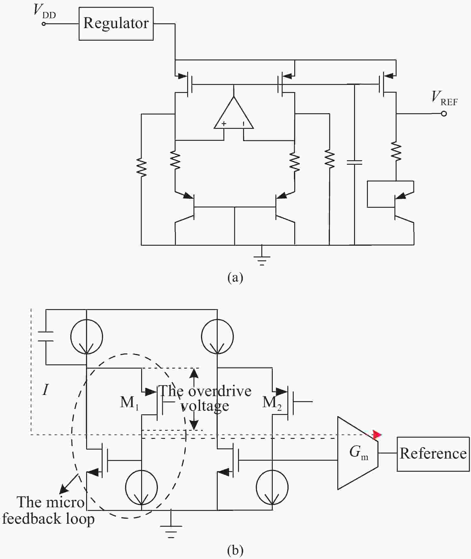
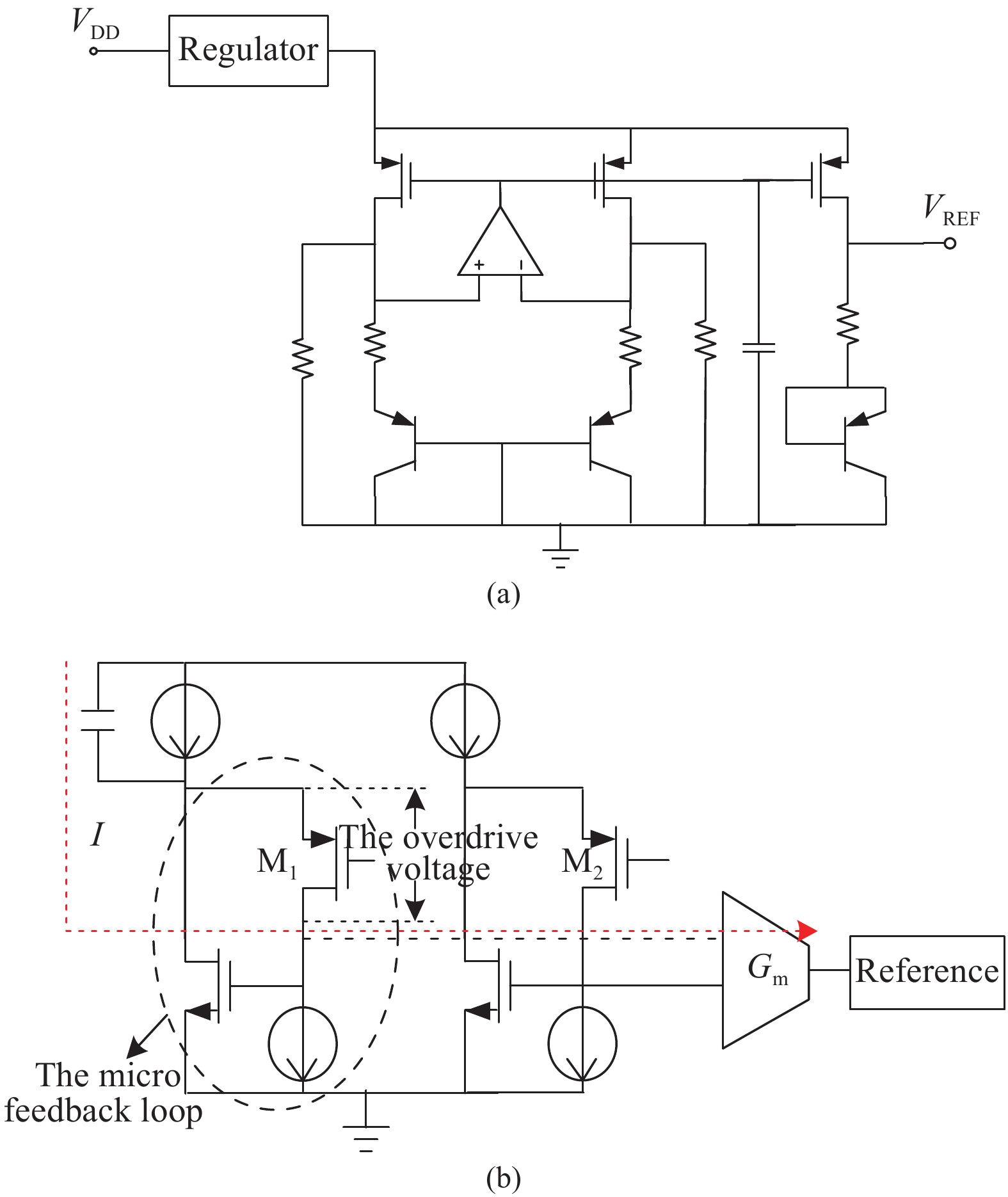
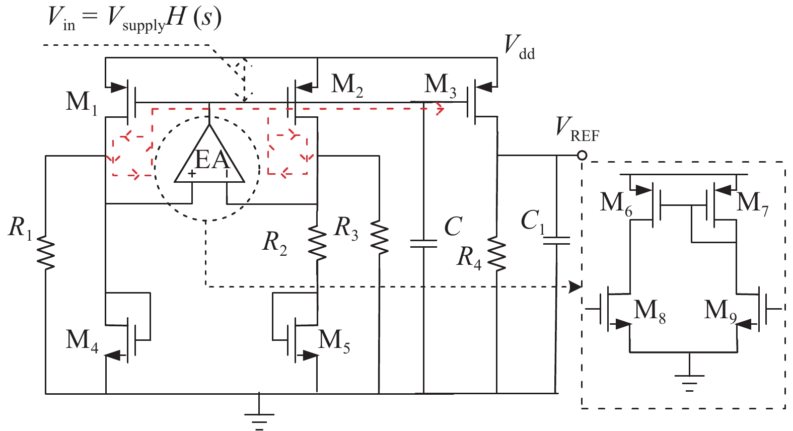
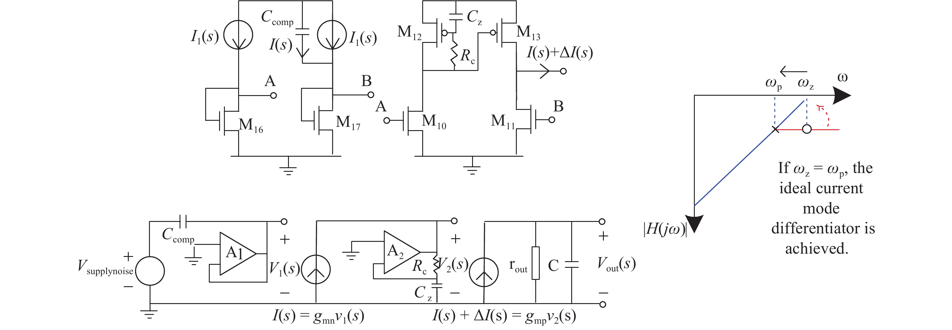
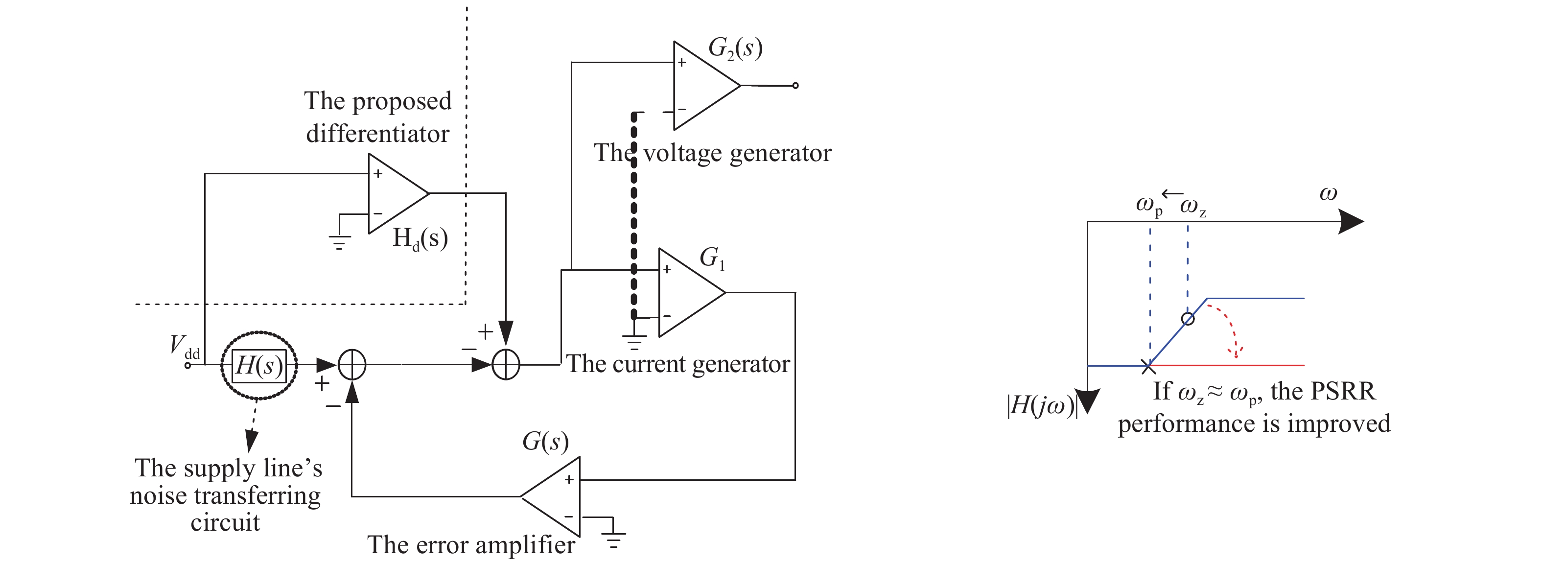
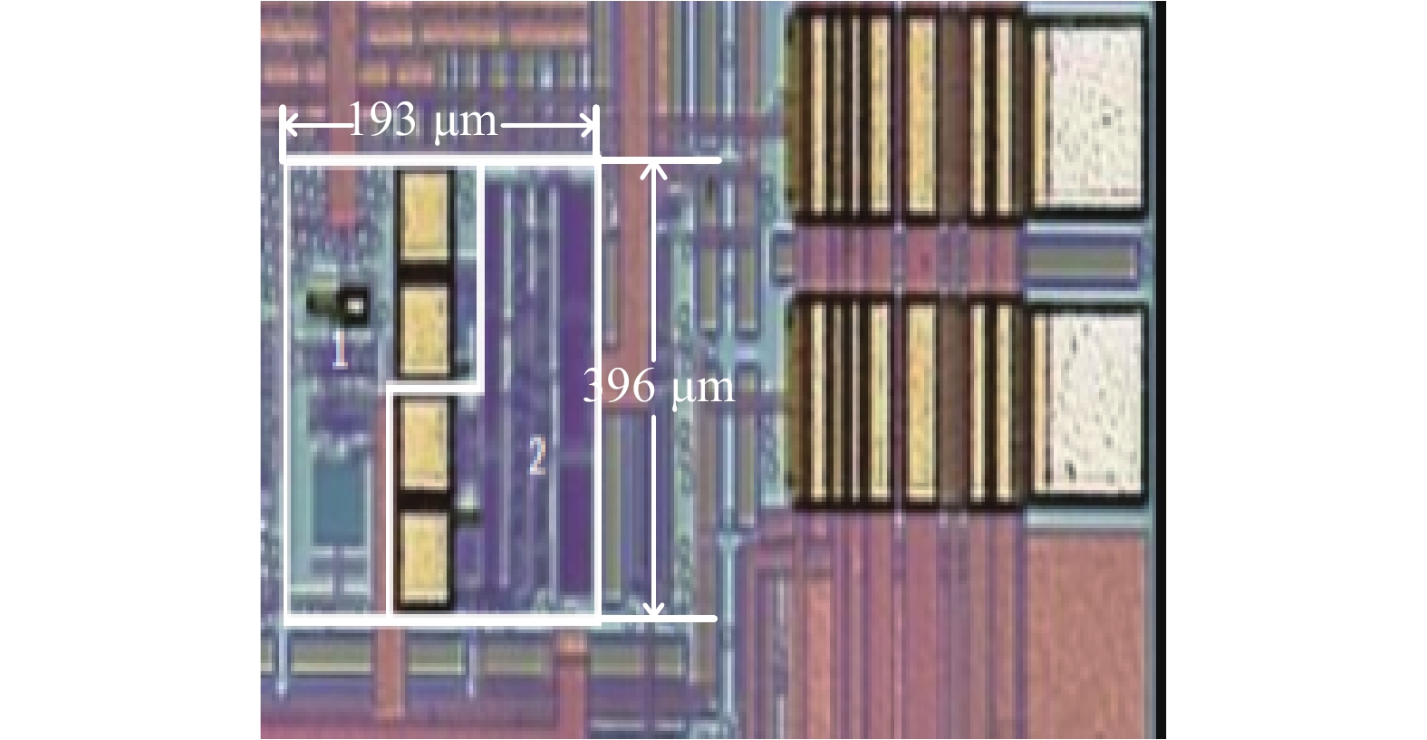
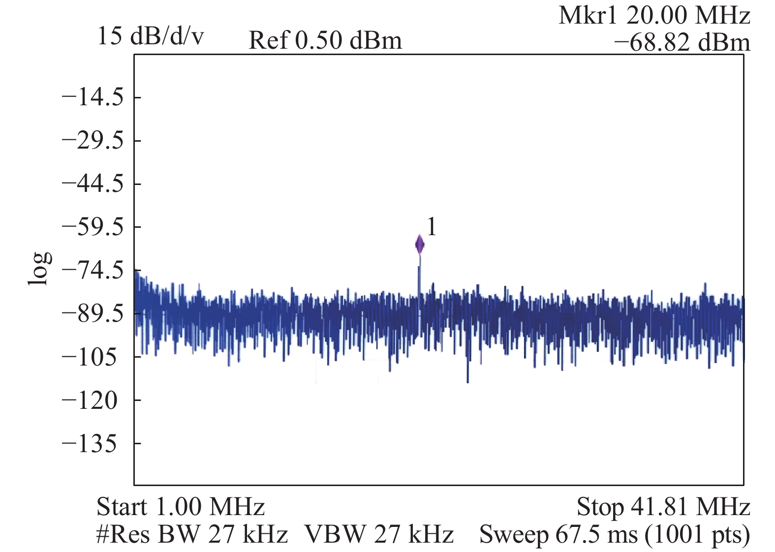
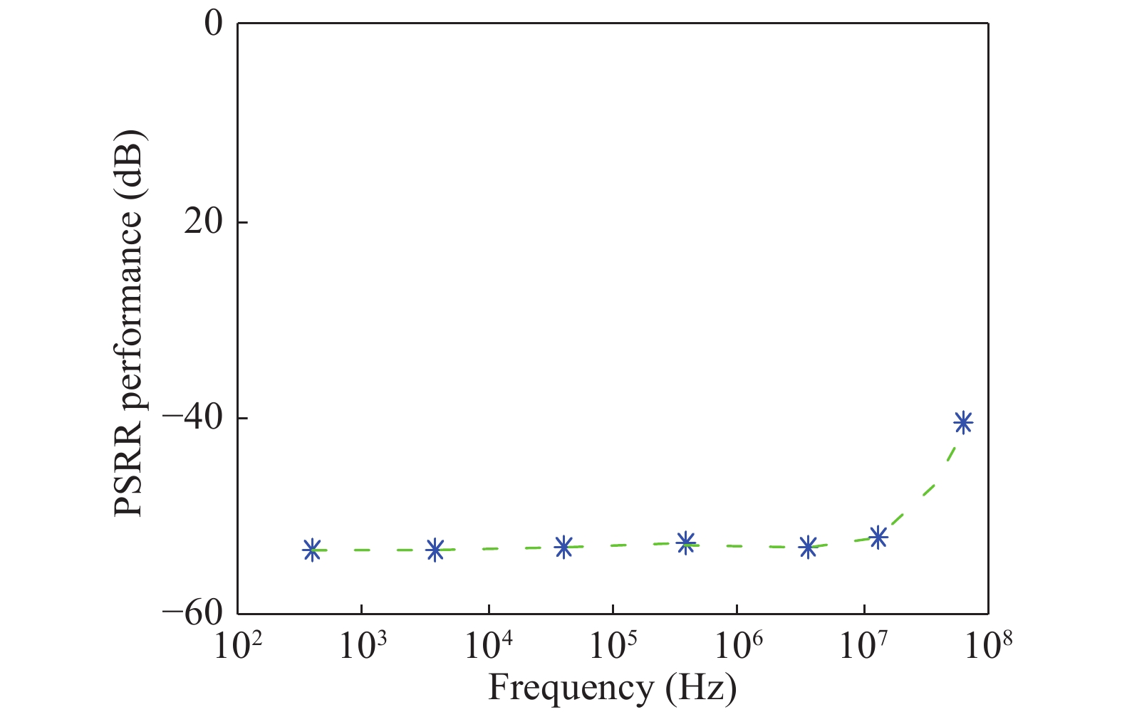
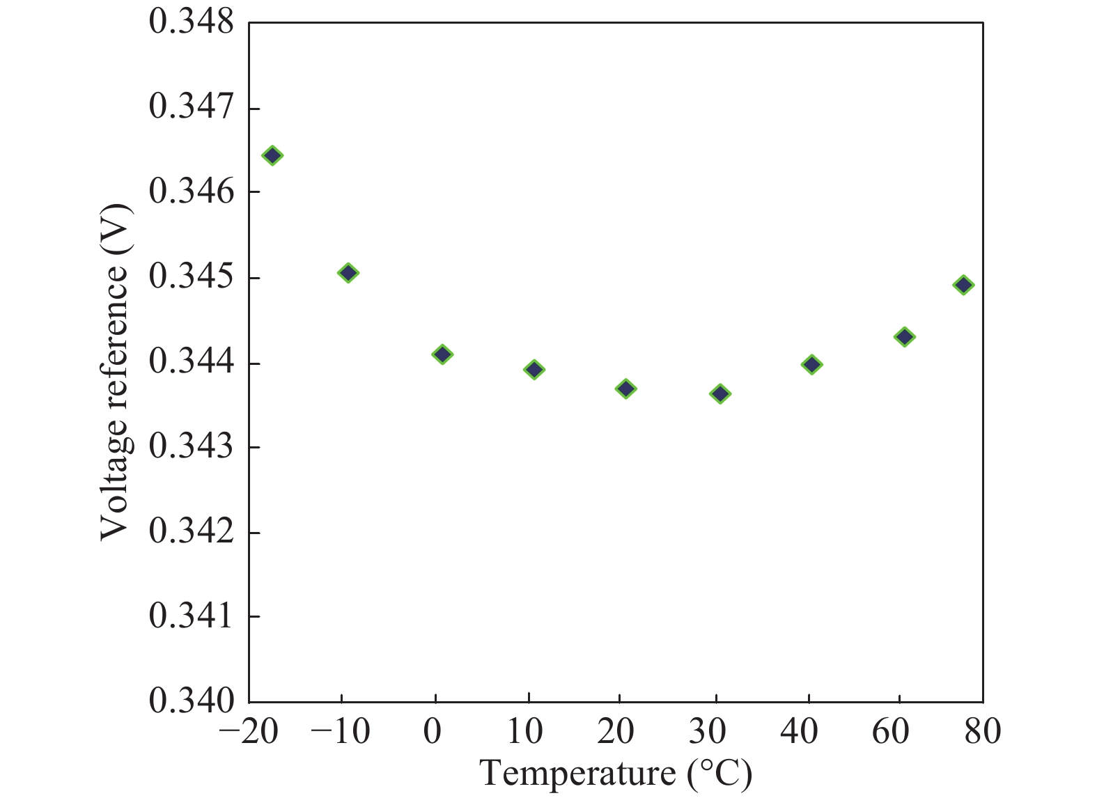
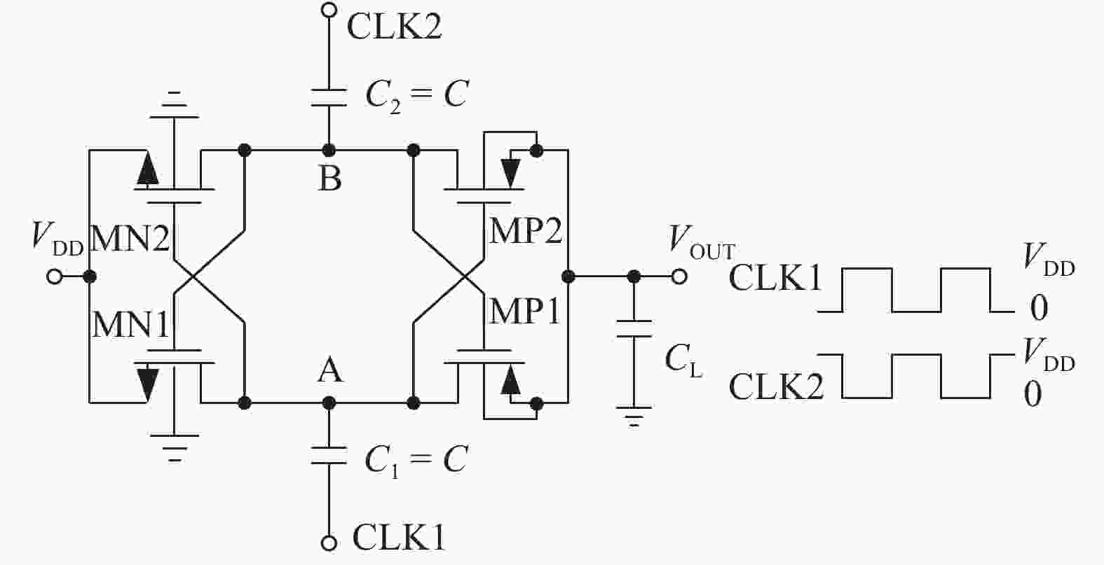
We present a voltage reference using a wide-band cascaded current mode differentiator, for the improved PSRR performance. Compared with the conventional references, the reference with the technique is mainly characterized by a two cascaded stages current mode signal differentiator. In the differentiator, a zero OTA Gm is proposed, to achieve the wide-band differential characteristic. With the technique, the PSRR beyond the pole’s corresponding frequency can be significantly improved with the minimum supply voltage only about VGS_PMOS + (VGS_NMOS − VTH). Fabricated with a 0.18 μm CMOS process, with the 0.9 V supply voltage, the PSRR @ 20 MHz of the reference is achieved at −54 dB. Moreover, the power dissipation is 19 μW.


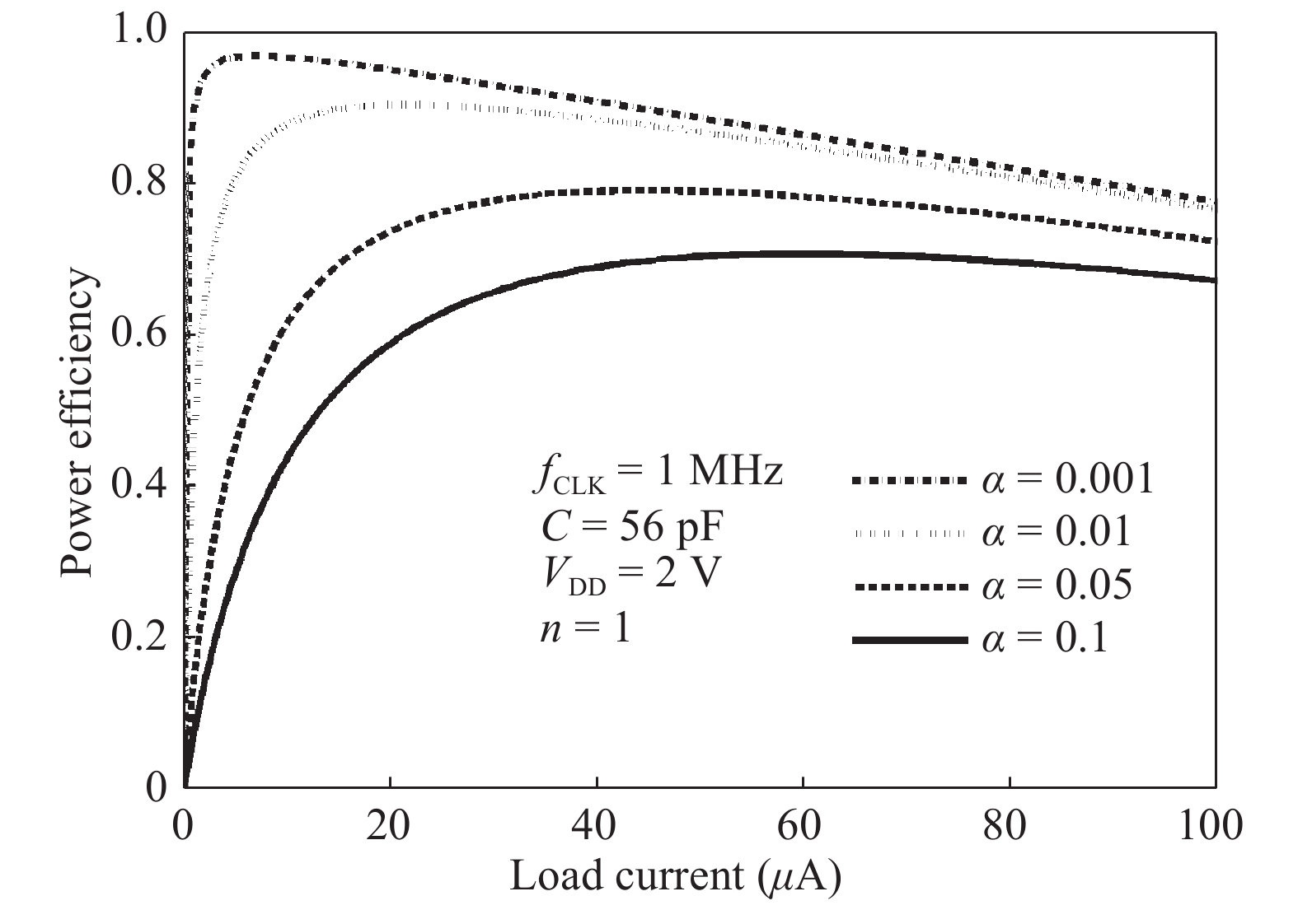
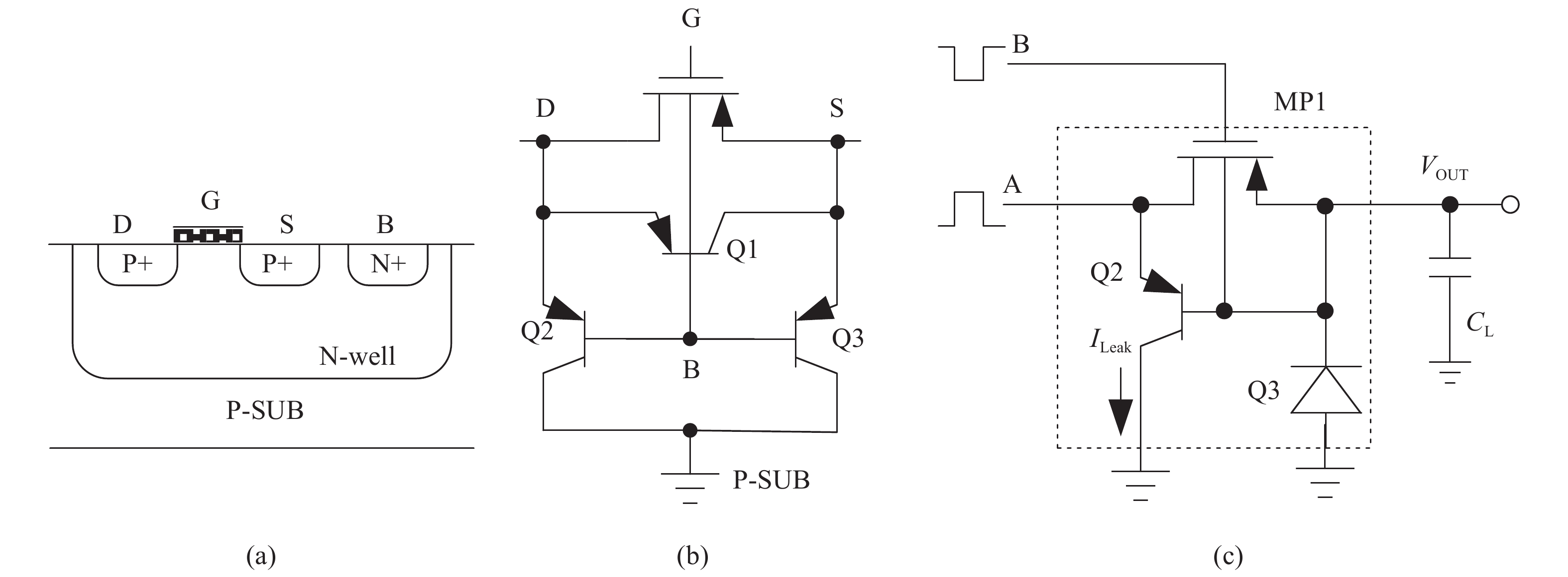
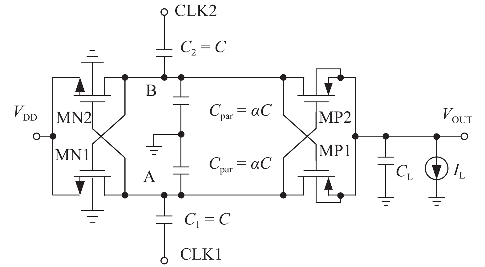
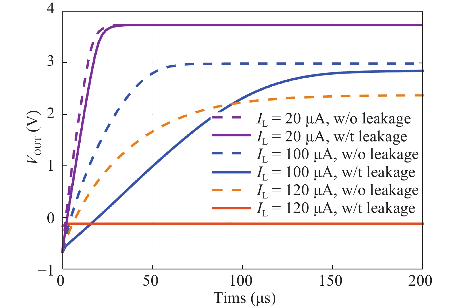
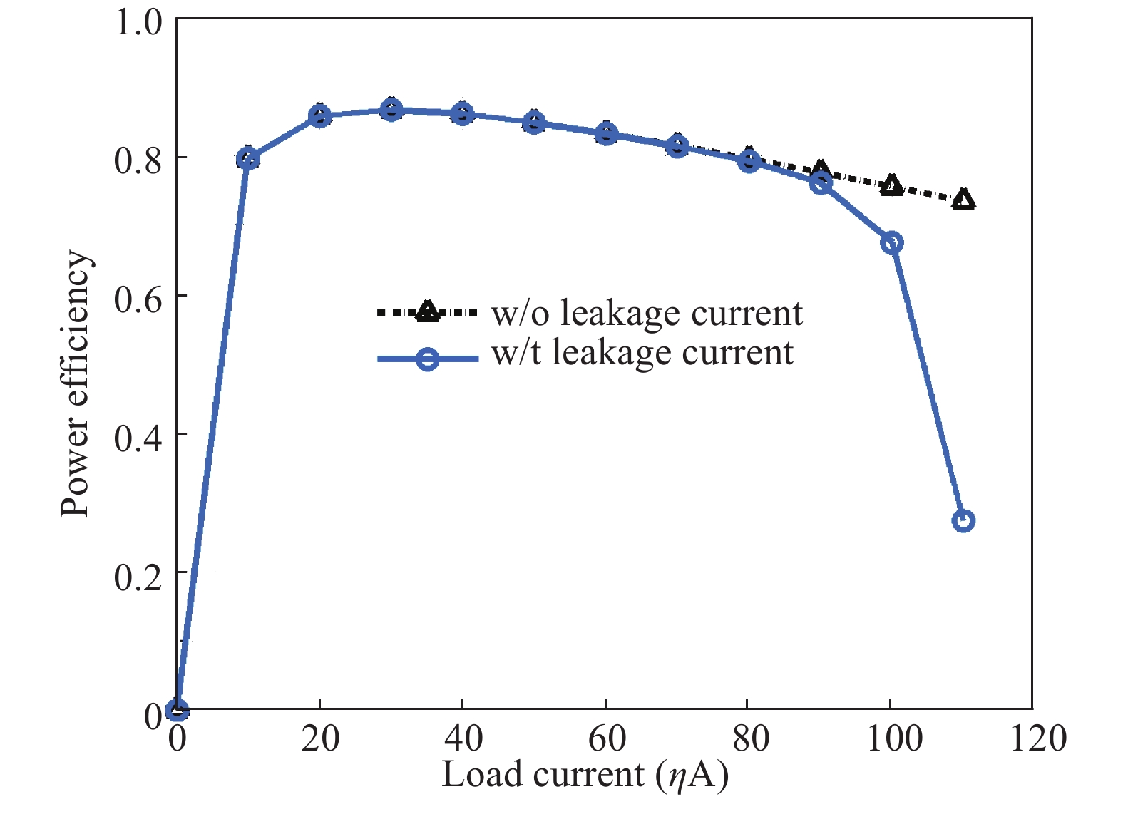
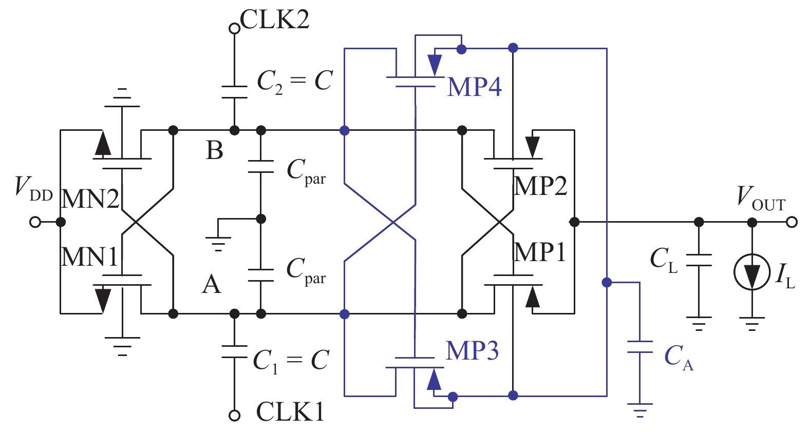
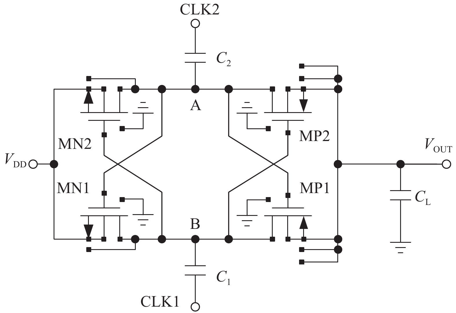
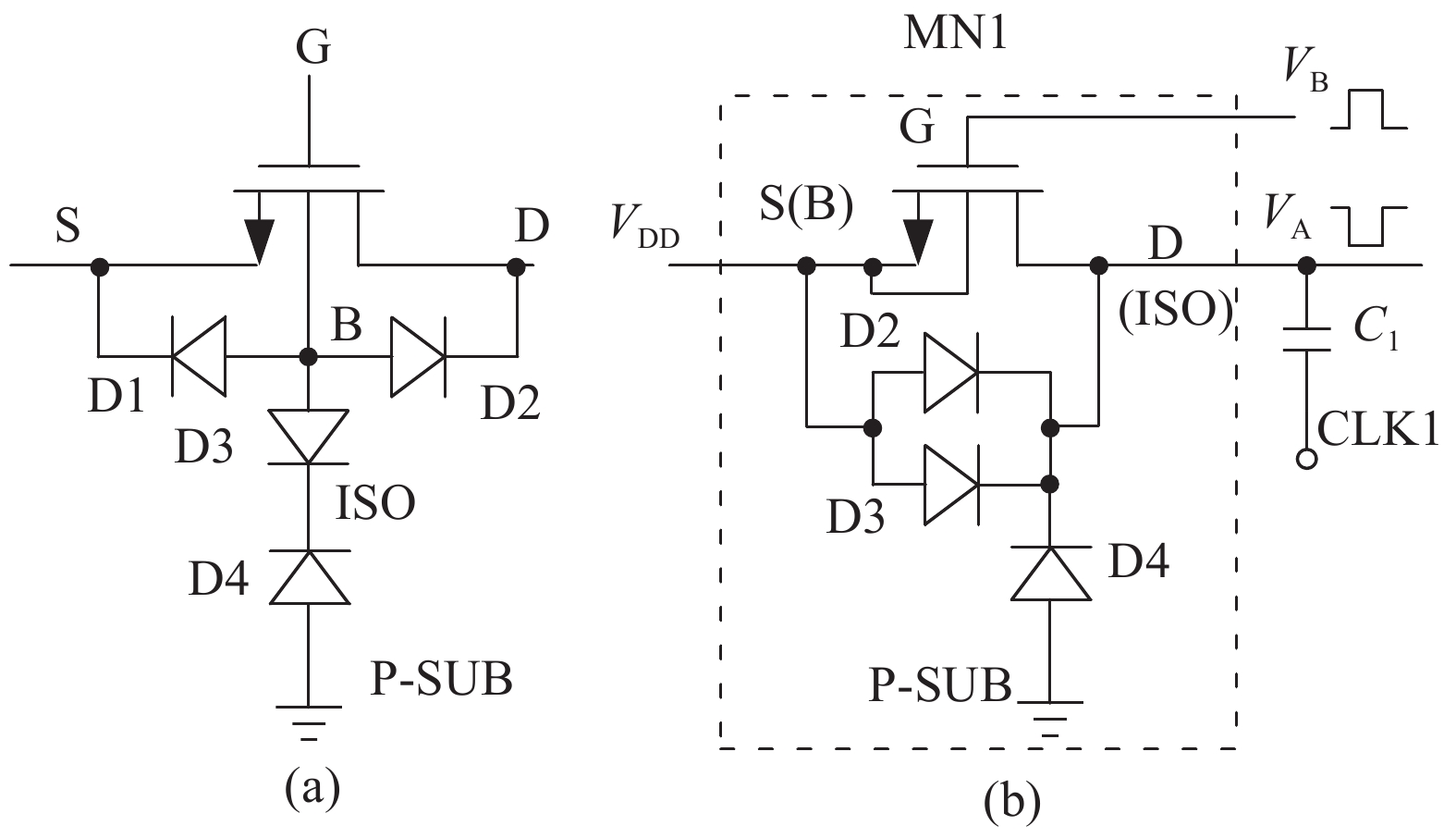
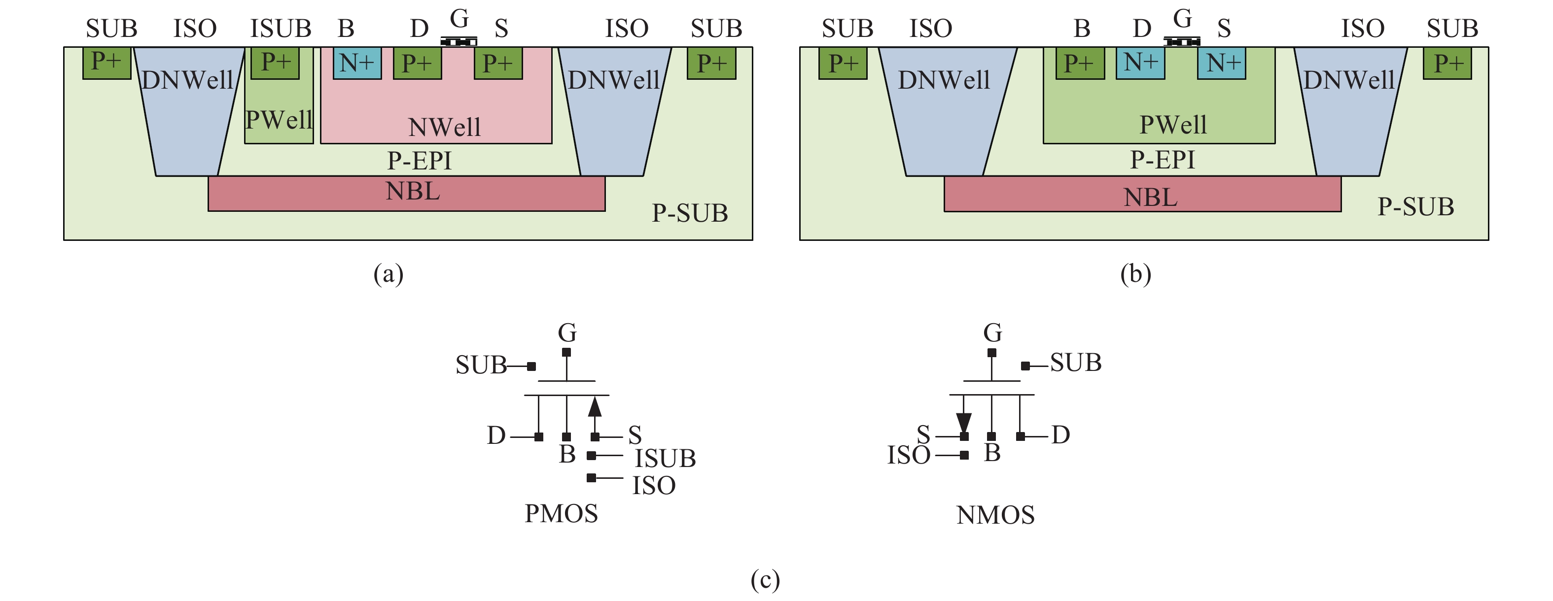
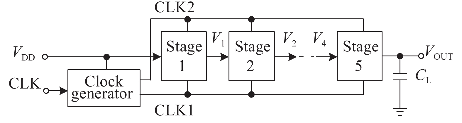
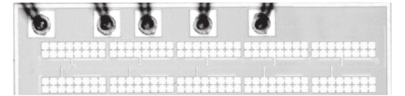
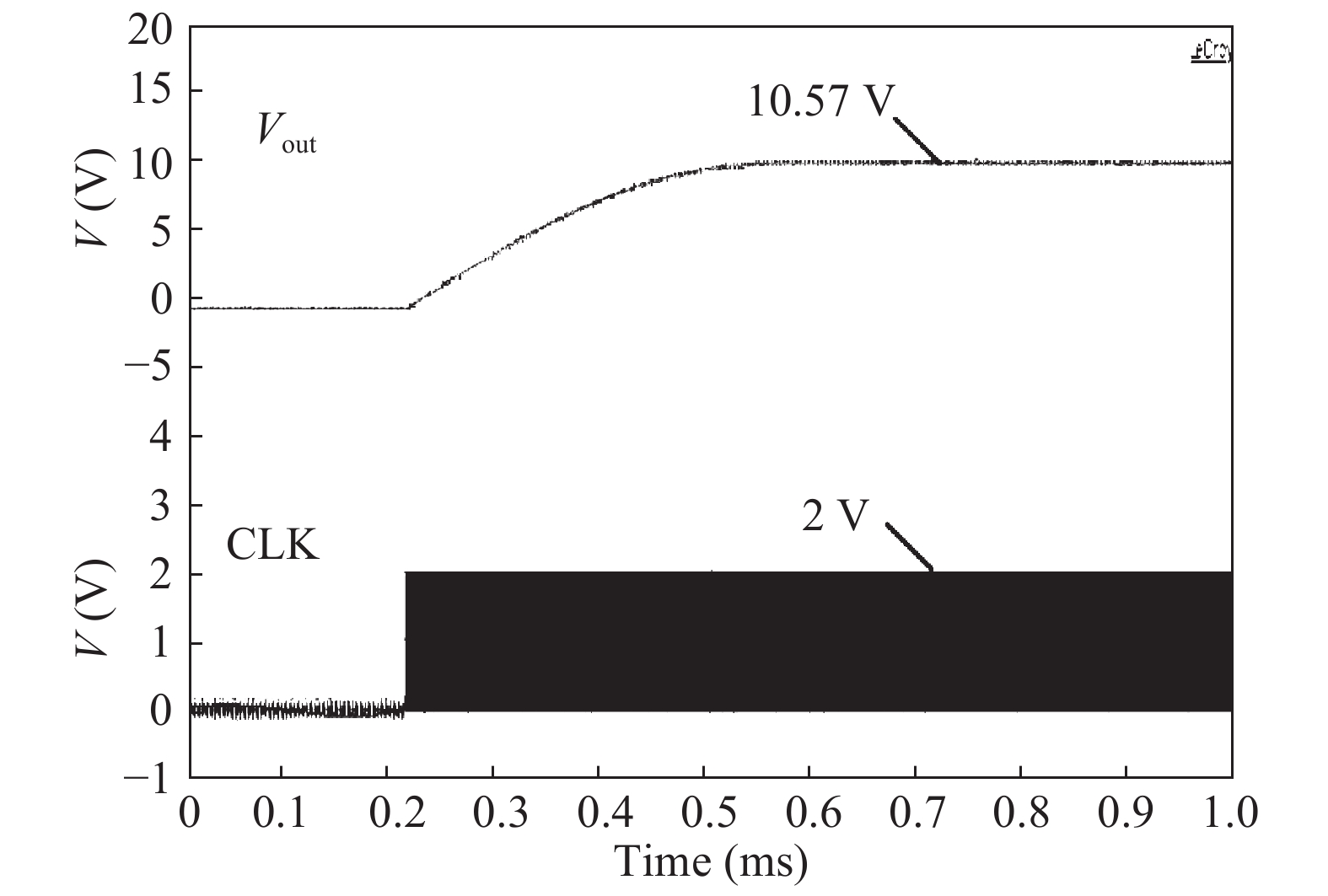
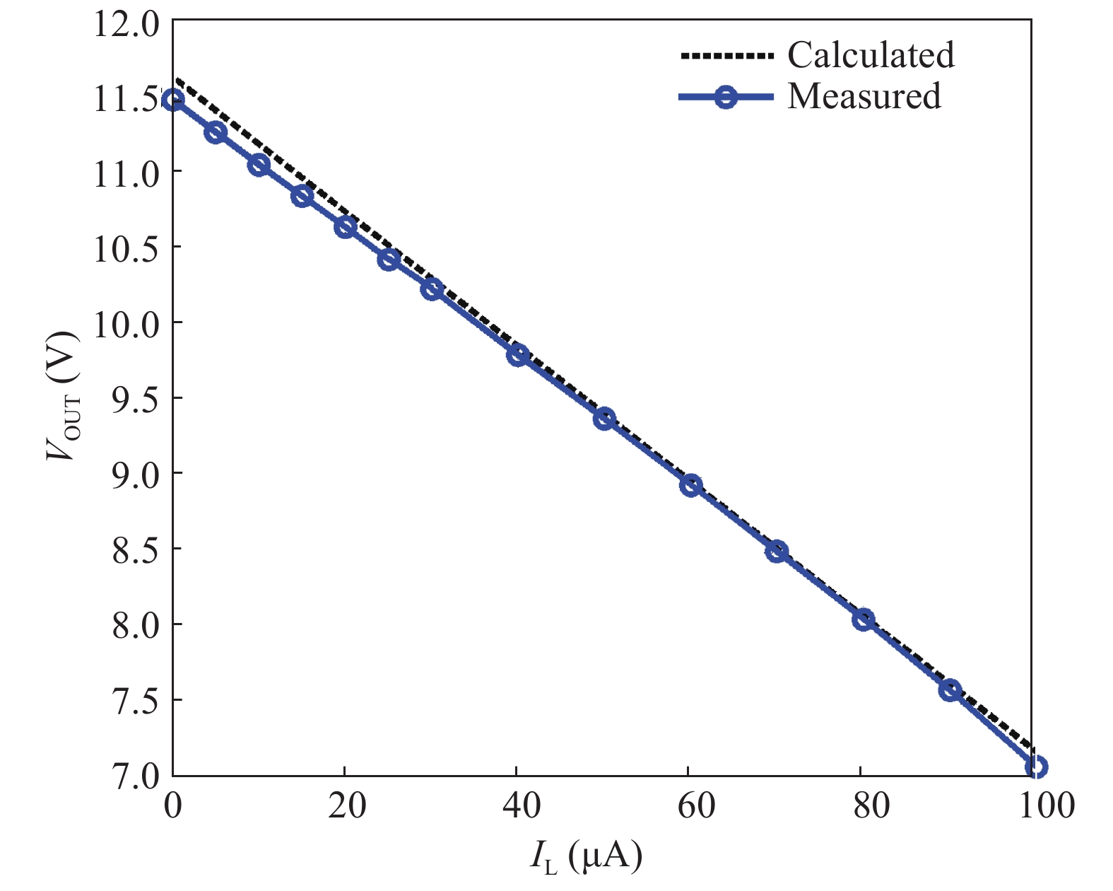
This paper presents a high-efficiency charge pump circuit composed of cascaded cross-coupled voltage doublers implemented in an isolated bipolar-CMOS-DMOS (BCD) technology for implantable medical devices. Taking advantage of the transistor structures in the isolated BCD process, the leakage currents caused by the parasitic PNP transistors in the cross-coupled PMOS serial switches are eliminated by simply connecting the inside substrate terminal to the isolation terminal of each PMOS transistor. The simple circuit structure leads to small parasitic capacitance in the voltage doubler, which in turn ensures high efficiency of the overall charge pump. The proposed charge pump with 5 cascaded voltage doublers is fabricated in a 0.35-μm isolated BCD process. Measurement results with 2-V power supply, 1-MHz driving clock frequency and 40-μA current load show that an efficiency of 72.6% is achieved, and the output voltage can be pumped to about 11.5 V at zero load current. The chip area of the charge pump is 1.6 × 0.35 mm2.