ARTICLES

Vertical nanowire/nanosheet FETs with a horizontal channel for threshold voltage modulation

Yongbo Liu1, 2, Huilong Zhu1, 2, 3, , Yongkui Zhang1, , Xiaolei Wang1, Weixing Huang1, 2, Chen Li1, 2, Xuezheng Ai1 and Qi Wang1

+ Author Affiliations

 Corresponding author: Huilong Zhu, zhuhuilong@ime.ac.cn; Yongkui Zhang, zhangyongkui@ime.ac.cn

PDF

Turn off MathJax

Abstract: A new type of vertical nanowire (VNW)/nanosheet (VNS) FETs combining a horizontal channel (HC) with bulk/back-gate electrode configuration, including Bulk-HC and FD-SOI-HC VNWFET, is proposed and investigated by TCAD simulation. Comparisons were carried out between conventional VNWFET and the proposed devices. FD-SOI-HC VNWFET exhibits better Ion/Ioff ratio and DIBL than Bulk-HC VNWFET. The impact of channel doping and geometric parameters on the electrical characteristic and body factor (γ) of the devices was investigated. Moreover, threshold voltage modulation by bulk/back-gate bias was implemented and a large γ is achieved for wide range Vth modulation. In addition, results of Ion enhancement and Ioff reduction indicate the proposed devices are promising candidates for performance and power optimization of NW/NS circuits by adopting dynamic threshold voltage management. The results of preliminary experimental data are discussed as well.

Key words: vertical nanowirenanosheetsilicon on insulator (SOI)threshold voltagemulti-Vththreshold voltage modulation


[1]
Hisamoto D, Lee W C, Kedzierski J, et al. FinFET – a self-aligned double-gate MOSFET scalable to 20 nm. IEEE Trans Electron Devices, 2000, 47, 2320 doi: 10.1109/16.887014
[2]
Loubet N, Hook T, Montanini P, et al. Stacked nanosheet gate-all-around transistor to enable scaling beyond FinFET. 2017 Symposium on VLSI Technology, 2017, 230 doi: 10.23919/VLSIT.2017.7998183
[3]
Ritzenthaler R, Mertens H, Pena V, et al. Vertically stacked gate-all-around Si nanowire CMOS transistors with reduced vertical nanowires separation, new work function metal gate solutions, and DC/AC performance optimization. 2018 IEEE International Electron Devices Meeting (IEDM), 2018, 21.5.1 doi: 10.1109/IEDM.2018.8614528
[4]
International Roadmap for Devices and Systems 2017 Edition More Moore, 2017. [Online]. Available: https://irds.ieee.org/editions/2017
[5]
Yakimets D, Eneman G, Schuddinck P, et al. Vertical GAAFETs for the ultimate CMOS scaling. IEEE Trans Electron Devices, 2015, 62, 1433 doi: 10.1109/TED.2015.2414924
[6]
Pan C Y, Raghavan P, Yakimets D, et al. Technology/system codesign and benchmarking for lateral and vertical GAA nanowire FETs at 5-nm technology node. IEEE Trans Electron Devices, 2015, 62, 3125 doi: 10.1109/TED.2015.2461457
[7]
Kwong D L, Li X, Sun Y, et al. Vertical silicon nanowire platform for low power electronics and clean energy applications. J Nanotechnol, 2012, 2012, 1 doi: 10.1155/2012/492121
[8]
Veloso A, Altamirano-Sanchez E, Brus S, et al. Vertical nanowire FET integration and device aspects. ECS Trans, 2016, 72, 31 doi: 10.1149/07204.0031ecst
[9]
Bohr M , Fellow I S . Silicon technology leadership for the mobility era. Intel Developer Forum, 2012
[10]
Choi Y K, Chang L, Ranade P, et al. FinFET process refinements for improved mobility and gate work function engineering. Dig Int Electron Devices Meet, 2002, 259 doi: 10.1109/IEDM.2002.1175827
[11]
Pherson M R M. The adjustment of mos transistor threshold voltage by ion implantation. Appl Phys Lett, 1971, 18, 502 doi: 10.1063/1.1653513
[12]
Lee T, Rhee S J, Kang C, et al. Structural advantage for the EOT scaling and improved electron channel mobility by incorporating dysprosium oxide (Dy2O3) into HfO2 n-MOSFETs. IEEE Electron Device Lett, 2006, 27, 640 doi: 10.1109/LED.2006.879023
[13]
Park J W, Baik H K, Lim T, et al. Threshold voltage control of oxide nanowire transistors using nitrogen plasma treatment. Appl Phys Lett, 2010, 97, 203508 doi: 10.1063/1.3518485
[14]
Fried D M, Duster J S, Kornegay K T. Improved independent gate N-type FinFET fabrication and characterization. IEEE Electron Device Lett, 2003, 24, 592 doi: 10.1109/LED.2003.815946
[15]
Denton J P, Neudeck G W. Fully depleted dual-gated thin-film SOI P-MOSFETs fabricated in SOI islands with an isolated buried polysilicon backgate. IEEE Electron Device Lett, 1996, 17, 509 doi: 10.1109/55.541764
[16]
Liu Y X, Masahara M, Ishii K, et al. Flexible threshold voltage FinFETs with independent double gates and an ideal rectangular cross-section Si-Fin channel. IEEE International Electron Devices Meeting, 2003, 18.8.1 doi: 10.1109/IEDM.2003.1269445
[17]
Fried D M, Duster J S, Kornegay K T. High-performance p-type independent-gate FinFETs. IEEE Electron Device Lett, 2004, 25, 199 doi: 10.1109/LED.2004.825160
[18]
Kumar M P V, Lin J Y, Kao K H, et al. Junctionless FETs with a fin body for multi-VTH and dynamic threshold operation. IEEE Trans Electron Devices, 2018, 65, 3535 doi: 10.1109/TED.2018.2847355
[19]
Ota K, Saitoh M, Tanaka C, et al. Threshold voltage control by substrate bias in 10-nm-diameter tri-gate nanowire MOSFET on ultrathin BOX. IEEE Electron Device Lett, 2013, 34, 187 doi: 10.1109/LED.2012.2234719
[20]
Ohtou T, Saraya T, Hiramoto T. Variable-body-factor SOI MOSFET with ultrathin buried oxide for adaptive threshold voltage and leakage control. IEEE Trans Electron Devices, 2008, 55, 40 doi: 10.1109/TED.2007.912612
[21]
Pelloux-Prayer B, Blagojević M, Thomas O, et al. Planar fully depleted SOI technology: The convergence of high performance and low power towards multimedia mobile applications. 2012 IEEE Faible Tension Faible Consommation, 2012, 1 doi: 10.1109/FTFC.2012.6231742
[22]
Yin X G, Zhang Y K, Zhu H L, et al. Vertical sandwich gate-all-around field-effect transistors with self-aligned high-k metal gates and small effective-gate-length variation. IEEE Electron Device Lett, 2020, 41, 8 doi: 10.1109/LED.2019.2954537
[23]
Yin X G, Zhu H L, Zhao L H, et al. Study of isotropic and Si-selective quasi atomic layer etching of Si1– xGex. ECS J Solid State Sci Technol, 2020, 9, 034012 doi: 10.1149/2162-8777/ab80ae
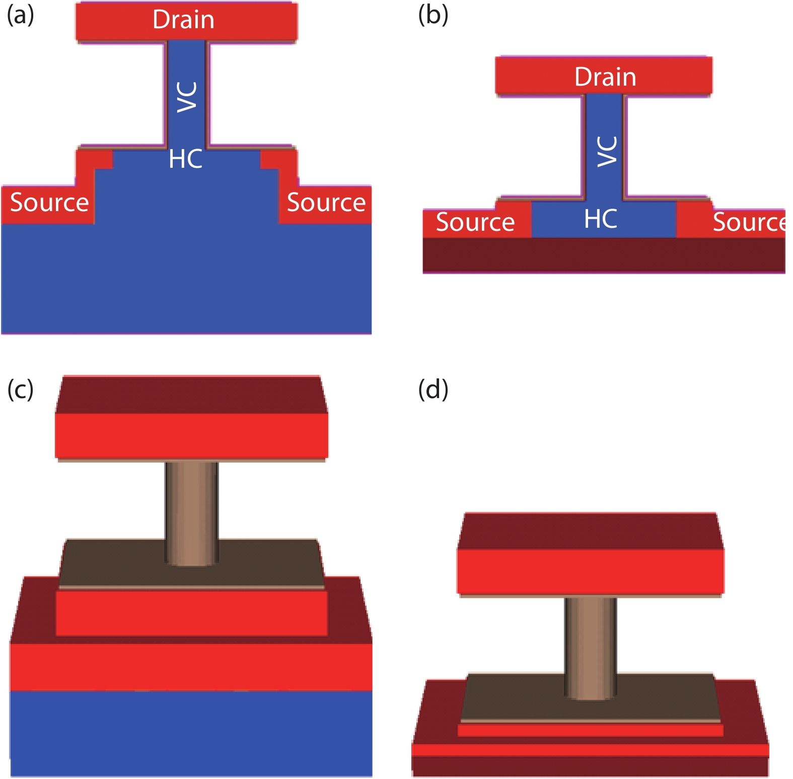
Fig. 1.  (Color online) Structures used in device simulations: (a) Cross-sectional view and (c) 3D structure of Bulk-HC VNWFET, (b) cross-sectional view and (d) 3D structure of FD-SOI-HC VNWFET. The positions of the vertical channel (VC) and horizontal channel (HC) are also indicated in the figure.

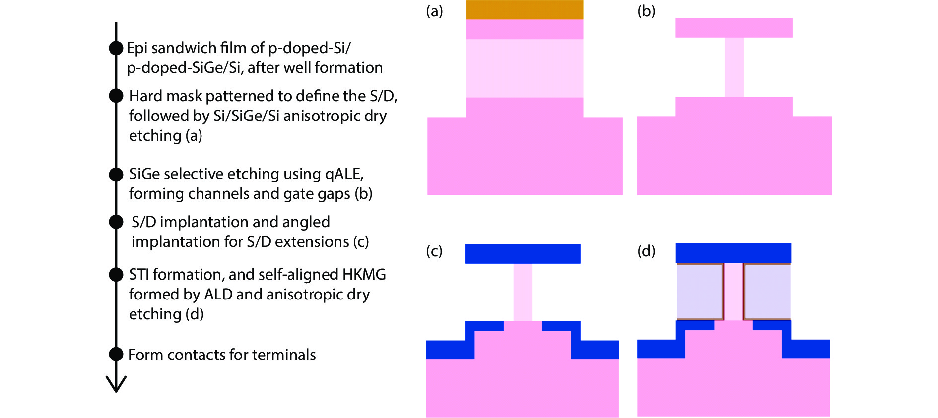
Fig. 2.  (Color online) Suggested process flow for the proposed Bulk-HC VNWFET.

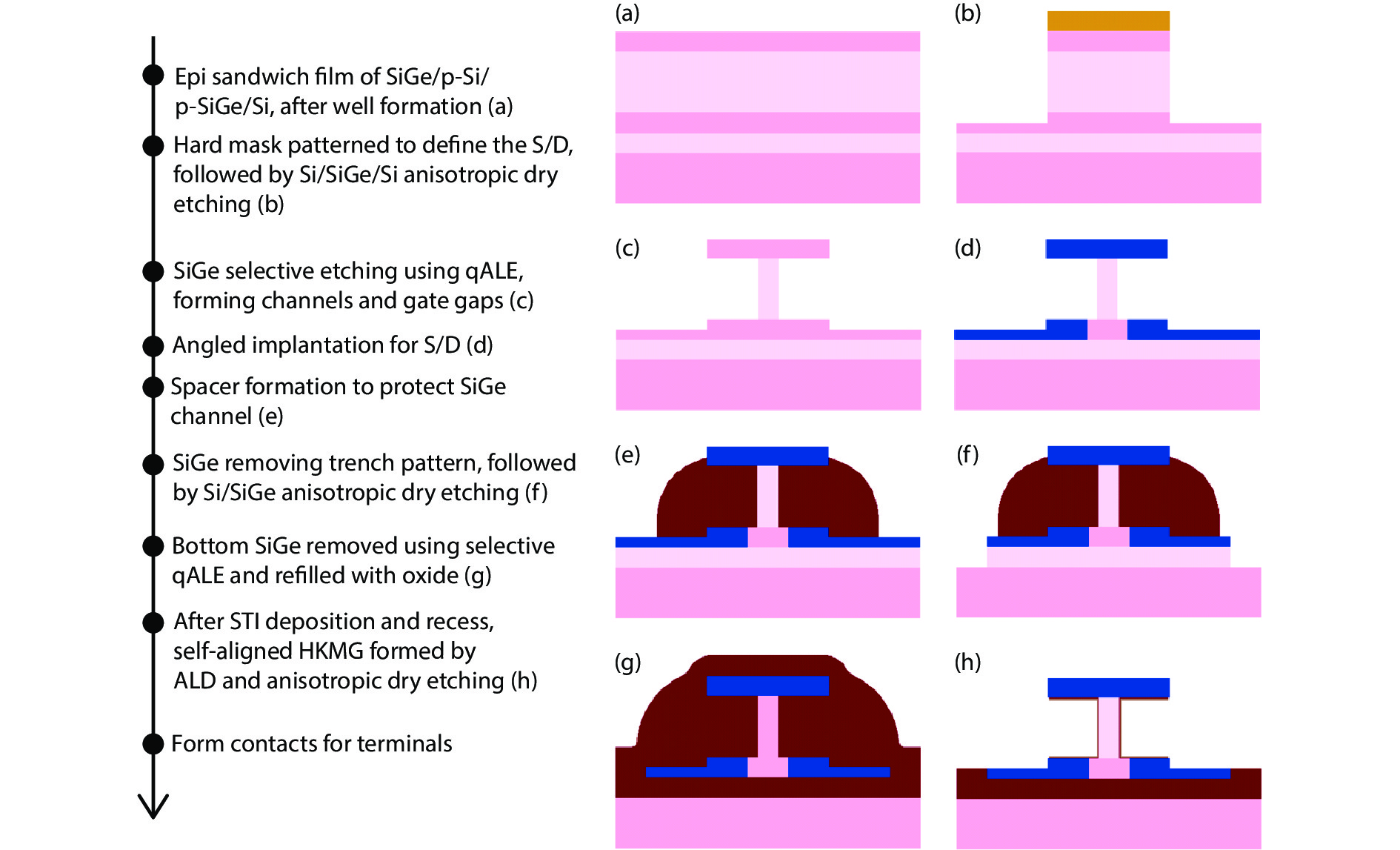
Fig. 3.  (Color online) Suggested process flow for the proposed FD-SOI-HC VNWFET.

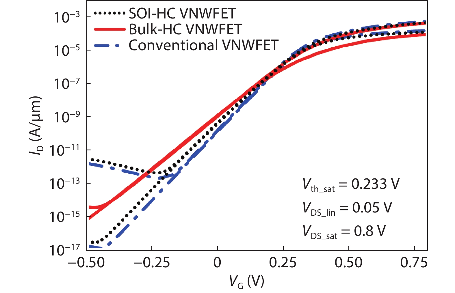
Fig. 4.  (Color online) Transfer characteristics of conventional, Bulk-HC and FD-SOI-HC VNWFETs. Channel doping concentration for conventional VNWFET: Na = 1 × 1015 cm–3. Channel doping concentration for Bulk-HC VNWFET: HC doping concentration Na = 2.5 × 1018 cm–3, VC doping concentration Na = 1 × 1015 cm–3. Channel doping concentration for FD-SOI-HC VNWFET: HC doping concentration Na = 1 × 1017 cm–3, VC doping concentration Na = 1 × 1015 cm–3. Threshold voltage has been modulated to the same value (Vth_sat = 0.233 V). LHC = 80 nm, LVC = 60 nm and Dnw = 20 nm.

Fig. 5.  (Color online) The electrostatic potential of (a) conventional VNWFET and (b) Bulk-HC VNWFET at VG = 0 V, VDS = 0.8 V and VB = 0 V.

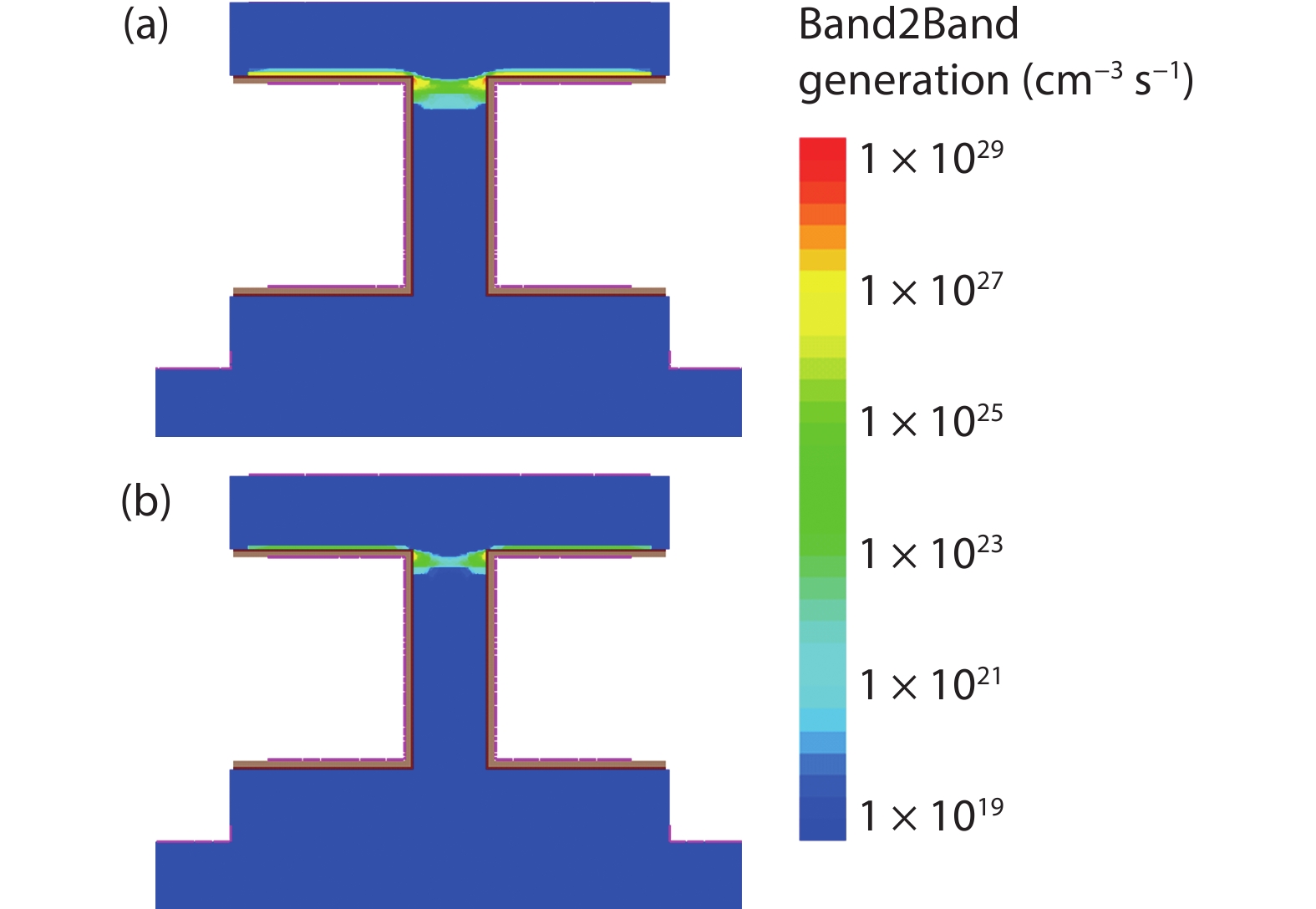
Fig. 6.  (Color online) BTBT generation rate of (a) conventional VNWFET and (b) Bulk-HC VNWFET at VG = – 0.5 V, VDS = 0.8 V and VB = 0 V.

Fig. 8.  (Color online) (a) Threshold voltage, body factor, and (b) SS, DIBL of Bulk-HC and FD-SOI-HC VNWFET for different VC doping concentration, with Bulk-HC VNWFET HC doping concentration Na = 2.5 × 1018 cm–3, FD-SOI-HC VNWFET HC doping concentration Na = 1 × 1017 cm–3, LHC = 80 nm, LVC = 60 nm and Dnw = 20 nm.

Fig. 9.  (Color online) (a) Threshold voltage, body factor, and (b) SS, DIBL of Bulk-HC and FD-SOI-HC VNSFET for different horizontal channel length, with Bulk-HC VNSFET HC doping concentration Na = 2.5 × 1018 cm–3 and VC doping concentration Na = 1 × 1015 cm–3, FD-SOI-HC VNSFET HC doping concentration Na = 1 × 1017 cm–3 and VC doping concentration Na = 1 × 1015 cm–3, LVC = 60 nm and Dnw = 20 nm

Fig. 7.  (Color online) (a) Threshold voltage, body factor, and (b) SS, DIBL of Bulk-HC and FD-SOI-HC VNWFET for different HC doping concentration, with VC doping concentration Na = 1 × 1015 cm–3, LHC = 80 nm, LVC = 60 nm and Dnw = 20 nm.

Fig. 10.  (Color online) (a) Threshold voltage, body factor, and (b) SS, DIBL of Bulk-HC and FD-SOI-HC VNSFET for different nanowire diameter, with Bulk-HC VNSFET HC doping concentration Na = 2.5 × 1018 cm–3 and VC doping concentration Na = 1 × 1015 cm–3, FD-SOI-HC VNSFET HC doping concentration Na = 1 × 1017 cm–3 and VC doping concentration Na = 1 × 1015 cm–3, LHC = 80 nm, LVC = 60 nm and Dnw = 20 nm.

Fig. 11.  (Color online) (a) Transfer characteristics of Bulk-HC and FD-SOI-HC VNWFETs for different bulk/back-gate bias VB, compared with a conventional VNWFET counterpart. (b) Extracted Ion (VG = 0.8 V, VDS = 0.8 V) and Ioff (VG = 0 V, VDS = 0.8 V) at different bulk/back-gate bias VB. Ion and Ioff can be adjusted by VB. Channel doping concentration are the same in section 3.3. LHC = 80 nm, LVC = 60 nm and Dnw = 20 nm.

Fig. 12.  (Color online) (a) Transfer characteristics of Bulk-HC and FD-SOI-HC VNSFETs for different bulk/back-gate bias VB, compared with a conventional VNWFET counterpart. (b) Extracted Ion (VG = 0.8 V, VDS = 0.8 V) and Ioff (VG = 0 V, VDS = 0.8 V) at different bulk/back-gate bias VB. LHC = 30 nm, LVC = 10 nm and Dnw = 5 nm.

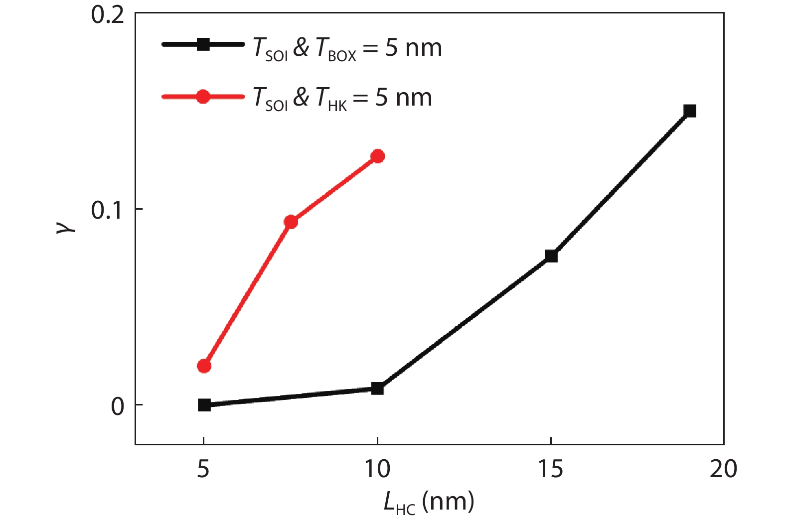
Fig. 13.  (Color online) Body factor of FD-SOI-HC VNSFET for different horizontal channel length, with LVC = 10 nm and Dnw = 5 nm.

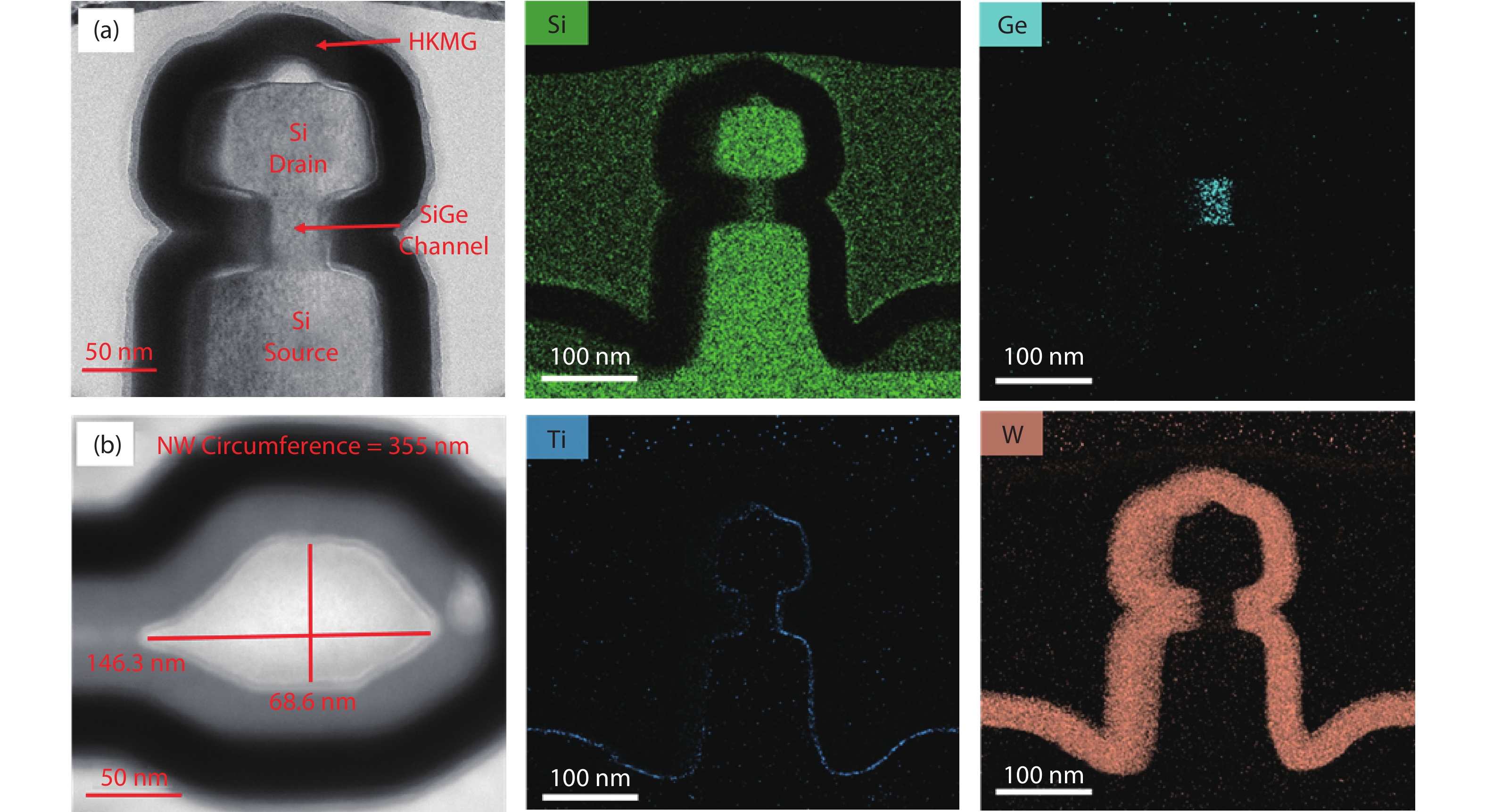
Fig. 14.  (Color online) Bulk-HC VNWFET TEM images of (a) cross-section and (b) top-view. And EDX mapping of the cross-section.

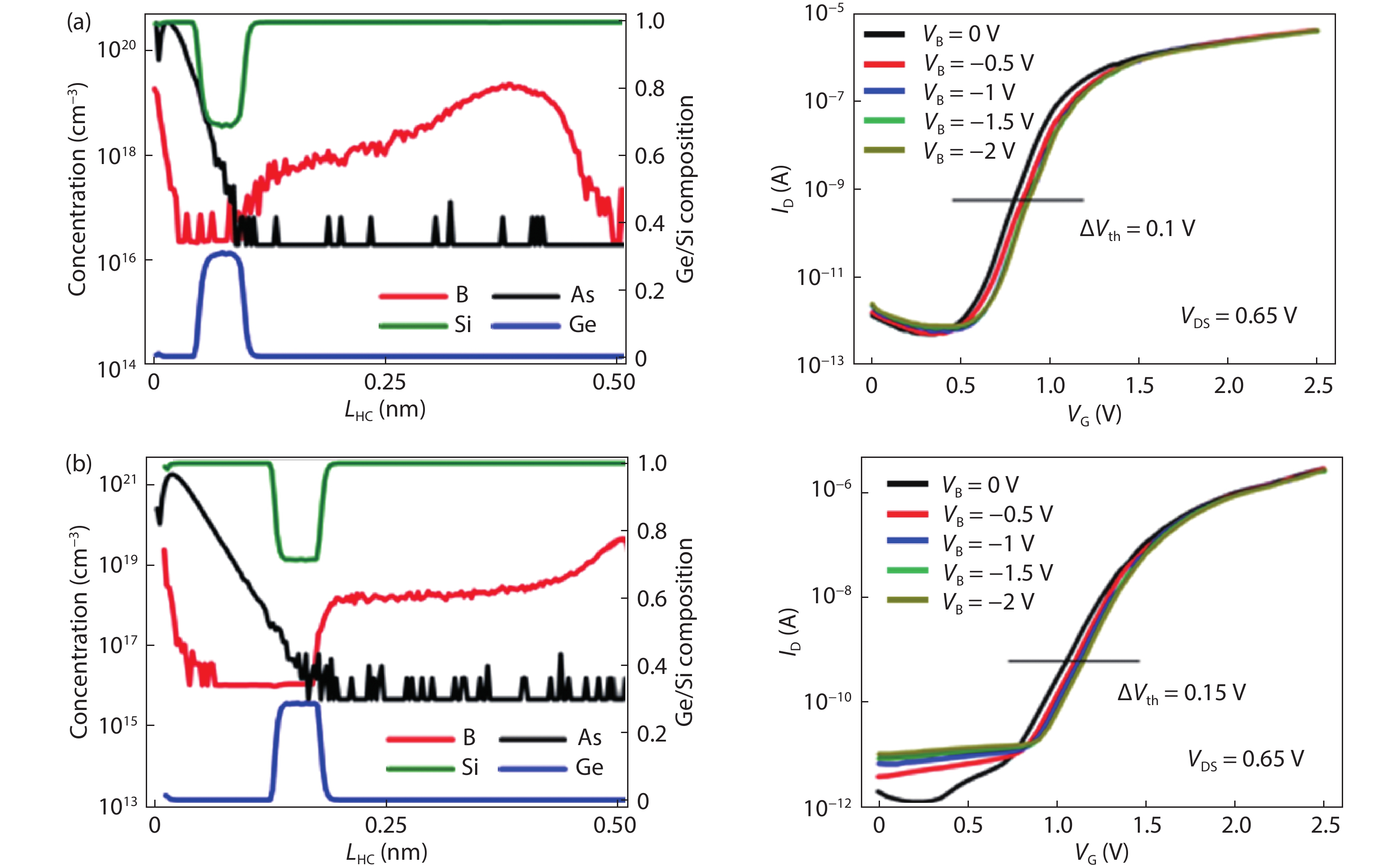
Fig. 15.  (Color online) SIMS profiles of two concentration conditions of B and As, and corresponding IDVG curves with different bulk bias. (a) S/D implantations of As with 2 × 1015 cm–2/7 keV/7° tilt angle and (b) S/D implantations of As with 2 × 1015 cm–2/17 keV/7° tilt angle.

Table 1.   Designed parameter values for transistors.

ParameterBulk-HC VNWFETsFD-SOI-HC VNWFETsConventional VNWFETs
VC length (LVC) (nm)110/6010/6060
Dnw (nm)5/10/20/30/405/10/20/30/4020
HC length (LHC) (nm)20/30/40/60/80/10020/30/40/60/80/100
S/D extension depth (nm)1010
SOI thickness (TSOI) (nm)10
BOX thickness (TBOX) (nm)10
VC doping (cm–3)1 × 10¹⁵ – 5 × 10181 × 1015 – 5 × 10181 × 1015
HC doping (cm–3)1 × 10¹⁷ – 5 × 10181 × 1017 – 5 × 10¹⁸
S/D doping (cm–3)1 × 10201 × 10201 × 1020
SiO2 (IL) thickness (nm)0.60.60.6
HfO2 thickness (nm)1.71.71.7
Work function (eV) 4.04.44.446
1 Definition of LVC corresponds to the gate length (LG) of conventional VNWFETs.
DownLoad: CSV

Table 2.   Extracted electrical characteristics.

Parameter Bulk-HC VNWFETFD-SOI-HC VNWFETConventional VNWFET
Vth (sat) (V)0.2330.2330.233
SSsat (mV/dec)79.7871.661.5
DIBL (mV/V)38513
Ion (A)4.35 × 10–44.65 × 10–45.69 × 10⁻⁴
Ioff (A)1.14 × 10–94.67 × 10–101.65 × 10⁻¹⁰
Ion/Ioff ratio3.81 × 1059.96 × 1053.45 × 106
DownLoad: CSV
[1]
Hisamoto D, Lee W C, Kedzierski J, et al. FinFET – a self-aligned double-gate MOSFET scalable to 20 nm. IEEE Trans Electron Devices, 2000, 47, 2320 doi: 10.1109/16.887014
[2]
Loubet N, Hook T, Montanini P, et al. Stacked nanosheet gate-all-around transistor to enable scaling beyond FinFET. 2017 Symposium on VLSI Technology, 2017, 230 doi: 10.23919/VLSIT.2017.7998183
[3]
Ritzenthaler R, Mertens H, Pena V, et al. Vertically stacked gate-all-around Si nanowire CMOS transistors with reduced vertical nanowires separation, new work function metal gate solutions, and DC/AC performance optimization. 2018 IEEE International Electron Devices Meeting (IEDM), 2018, 21.5.1 doi: 10.1109/IEDM.2018.8614528
[4]
International Roadmap for Devices and Systems 2017 Edition More Moore, 2017. [Online]. Available: https://irds.ieee.org/editions/2017
[5]
Yakimets D, Eneman G, Schuddinck P, et al. Vertical GAAFETs for the ultimate CMOS scaling. IEEE Trans Electron Devices, 2015, 62, 1433 doi: 10.1109/TED.2015.2414924
[6]
Pan C Y, Raghavan P, Yakimets D, et al. Technology/system codesign and benchmarking for lateral and vertical GAA nanowire FETs at 5-nm technology node. IEEE Trans Electron Devices, 2015, 62, 3125 doi: 10.1109/TED.2015.2461457
[7]
Kwong D L, Li X, Sun Y, et al. Vertical silicon nanowire platform for low power electronics and clean energy applications. J Nanotechnol, 2012, 2012, 1 doi: 10.1155/2012/492121
[8]
Veloso A, Altamirano-Sanchez E, Brus S, et al. Vertical nanowire FET integration and device aspects. ECS Trans, 2016, 72, 31 doi: 10.1149/07204.0031ecst
[9]
Bohr M , Fellow I S . Silicon technology leadership for the mobility era. Intel Developer Forum, 2012
[10]
Choi Y K, Chang L, Ranade P, et al. FinFET process refinements for improved mobility and gate work function engineering. Dig Int Electron Devices Meet, 2002, 259 doi: 10.1109/IEDM.2002.1175827
[11]
Pherson M R M. The adjustment of mos transistor threshold voltage by ion implantation. Appl Phys Lett, 1971, 18, 502 doi: 10.1063/1.1653513
[12]
Lee T, Rhee S J, Kang C, et al. Structural advantage for the EOT scaling and improved electron channel mobility by incorporating dysprosium oxide (Dy2O3) into HfO2 n-MOSFETs. IEEE Electron Device Lett, 2006, 27, 640 doi: 10.1109/LED.2006.879023
[13]
Park J W, Baik H K, Lim T, et al. Threshold voltage control of oxide nanowire transistors using nitrogen plasma treatment. Appl Phys Lett, 2010, 97, 203508 doi: 10.1063/1.3518485
[14]
Fried D M, Duster J S, Kornegay K T. Improved independent gate N-type FinFET fabrication and characterization. IEEE Electron Device Lett, 2003, 24, 592 doi: 10.1109/LED.2003.815946
[15]
Denton J P, Neudeck G W. Fully depleted dual-gated thin-film SOI P-MOSFETs fabricated in SOI islands with an isolated buried polysilicon backgate. IEEE Electron Device Lett, 1996, 17, 509 doi: 10.1109/55.541764
[16]
Liu Y X, Masahara M, Ishii K, et al. Flexible threshold voltage FinFETs with independent double gates and an ideal rectangular cross-section Si-Fin channel. IEEE International Electron Devices Meeting, 2003, 18.8.1 doi: 10.1109/IEDM.2003.1269445
[17]
Fried D M, Duster J S, Kornegay K T. High-performance p-type independent-gate FinFETs. IEEE Electron Device Lett, 2004, 25, 199 doi: 10.1109/LED.2004.825160
[18]
Kumar M P V, Lin J Y, Kao K H, et al. Junctionless FETs with a fin body for multi-VTH and dynamic threshold operation. IEEE Trans Electron Devices, 2018, 65, 3535 doi: 10.1109/TED.2018.2847355
[19]
Ota K, Saitoh M, Tanaka C, et al. Threshold voltage control by substrate bias in 10-nm-diameter tri-gate nanowire MOSFET on ultrathin BOX. IEEE Electron Device Lett, 2013, 34, 187 doi: 10.1109/LED.2012.2234719
[20]
Ohtou T, Saraya T, Hiramoto T. Variable-body-factor SOI MOSFET with ultrathin buried oxide for adaptive threshold voltage and leakage control. IEEE Trans Electron Devices, 2008, 55, 40 doi: 10.1109/TED.2007.912612
[21]
Pelloux-Prayer B, Blagojević M, Thomas O, et al. Planar fully depleted SOI technology: The convergence of high performance and low power towards multimedia mobile applications. 2012 IEEE Faible Tension Faible Consommation, 2012, 1 doi: 10.1109/FTFC.2012.6231742
[22]
Yin X G, Zhang Y K, Zhu H L, et al. Vertical sandwich gate-all-around field-effect transistors with self-aligned high-k metal gates and small effective-gate-length variation. IEEE Electron Device Lett, 2020, 41, 8 doi: 10.1109/LED.2019.2954537
[23]
Yin X G, Zhu H L, Zhao L H, et al. Study of isotropic and Si-selective quasi atomic layer etching of Si1– xGex. ECS J Solid State Sci Technol, 2020, 9, 034012 doi: 10.1149/2162-8777/ab80ae
  • Search

    Advanced Search >>

    GET CITATION

    shu

    Export: BibTex EndNote

    Article Metrics

    Article views: 2339 Times PDF downloads: 177 Times Cited by: 0 Times

    History

    Received: 21 May 2021 Revised: 16 July 2021 Online: Accepted Manuscript: 25 October 2021Uncorrected proof: 02 November 2021Published: 04 January 2022

    Catalog

      Email This Article

      User name:
      Email:*请输入正确邮箱
      Code:*验证码错误
      Yongbo Liu, Huilong Zhu, Yongkui Zhang, Xiaolei Wang, Weixing Huang, Chen Li, Xuezheng Ai, Qi Wang. Vertical nanowire/nanosheet FETs with a horizontal channel for threshold voltage modulation[J]. Journal of Semiconductors, 2022, 43(1): 014101. doi: 10.1088/1674-4926/43/1/014101 Y B Liu, H L Zhu, Y K Zhang, X L Wang, W X Huang, C Li, X Z Ai, Q Wang, Vertical nanowire/nanosheet FETs with a horizontal channel for threshold voltage modulation[J]. J. Semicond., 2022, 43(1): 014101. doi: 10.1088/1674-4926/43/1/014101.Export: BibTex EndNote
      Citation:
      Yongbo Liu, Huilong Zhu, Yongkui Zhang, Xiaolei Wang, Weixing Huang, Chen Li, Xuezheng Ai, Qi Wang. Vertical nanowire/nanosheet FETs with a horizontal channel for threshold voltage modulation[J]. Journal of Semiconductors, 2022, 43(1): 014101. doi: 10.1088/1674-4926/43/1/014101

      Y B Liu, H L Zhu, Y K Zhang, X L Wang, W X Huang, C Li, X Z Ai, Q Wang, Vertical nanowire/nanosheet FETs with a horizontal channel for threshold voltage modulation[J]. J. Semicond., 2022, 43(1): 014101. doi: 10.1088/1674-4926/43/1/014101.
      Export: BibTex EndNote

      Vertical nanowire/nanosheet FETs with a horizontal channel for threshold voltage modulation

      doi: 10.1088/1674-4926/43/1/014101
      More Information
      • Author Bio:

        Yongbo Liu received the B.S. degree in electronic science and technology from JiLin university in2013. He is currently pursuing Ph.D degree in microelectronics and solid electronics at Institute of Microelectronics, Chinese Academy of Sciences. His research focuses on negative capacitance field effect transistor and silicon nanowire field effect transistor

        Huilong Zhu obtained his Ph.D degree in 1988 in physics at Beijing Normal University. He worked at Argonne National Laboratory in 1990-1992, University of Illinois at Urbana-Champaign in 1992–1996, Digital Equipment Corporation in 1996–1998, Intel in 1998–2000, and IBM in 2000–2009. Prof. Zhu joined the Institute of Microelectronics of Chinese Academy of Sciences in 2009. His research interests are mainly focused on advanced CMOS technology research

        Yongkui Zhang obtained his M.S degree in 2004 in Beijing University of science and technology. He worked at Semiconductor Manufacturing International Corporation in 2004– 2012. He joined the Institute of Microelectronics of Chinese Academy of Sciences in 2012. His research interests are mainly focused on advanced CMOS technology research

      • Corresponding author: zhuhuilong@ime.ac.cnzhangyongkui@ime.ac.cn
      • Received Date: 2021-05-21
      • Revised Date: 2021-07-16
      • Published Date: 2022-01-10

      Catalog

        /

        DownLoad:  Full-Size Img  PowerPoint
        Return
        Return