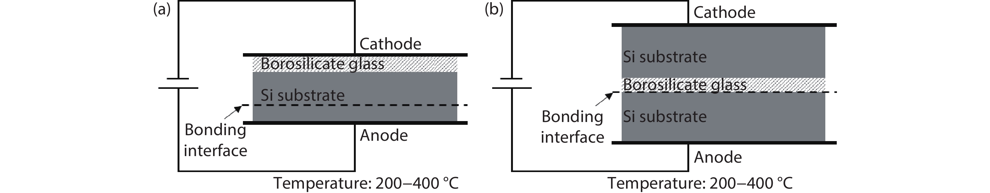
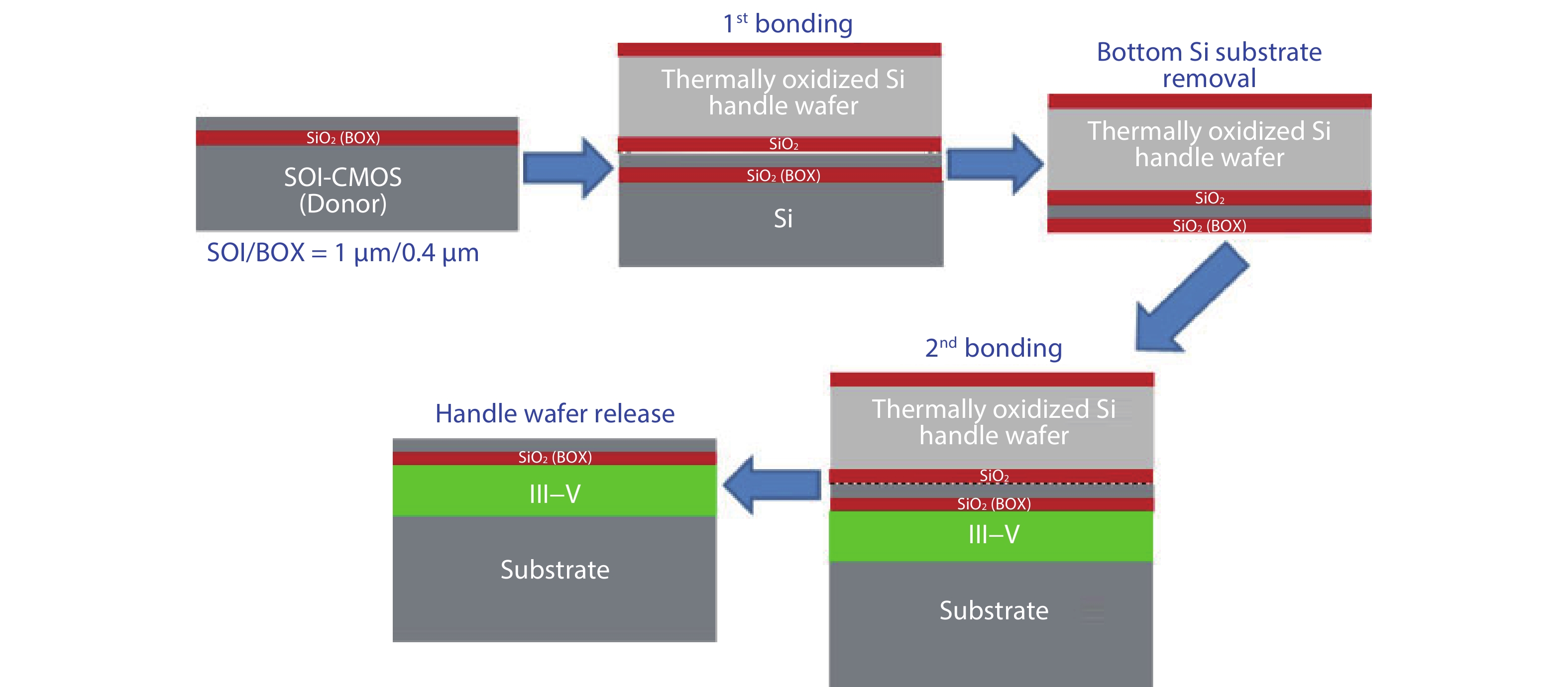
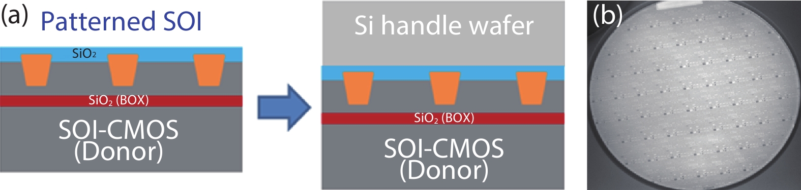
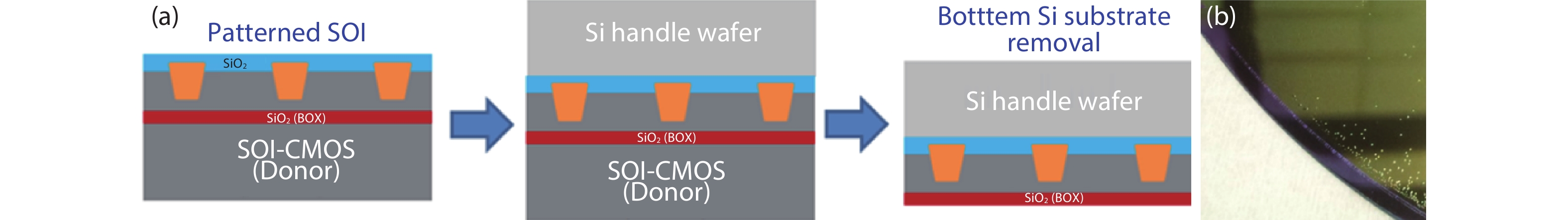
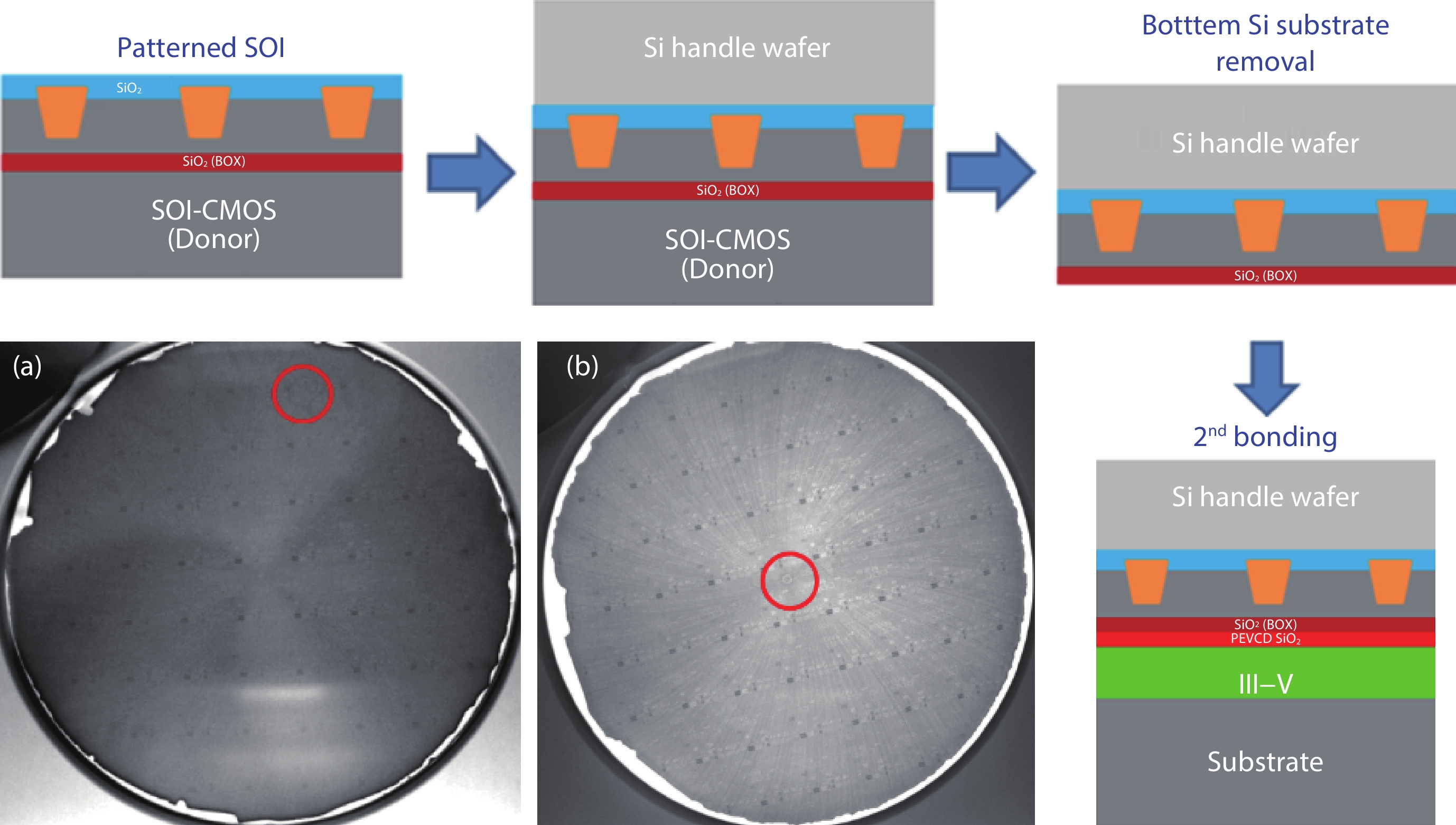
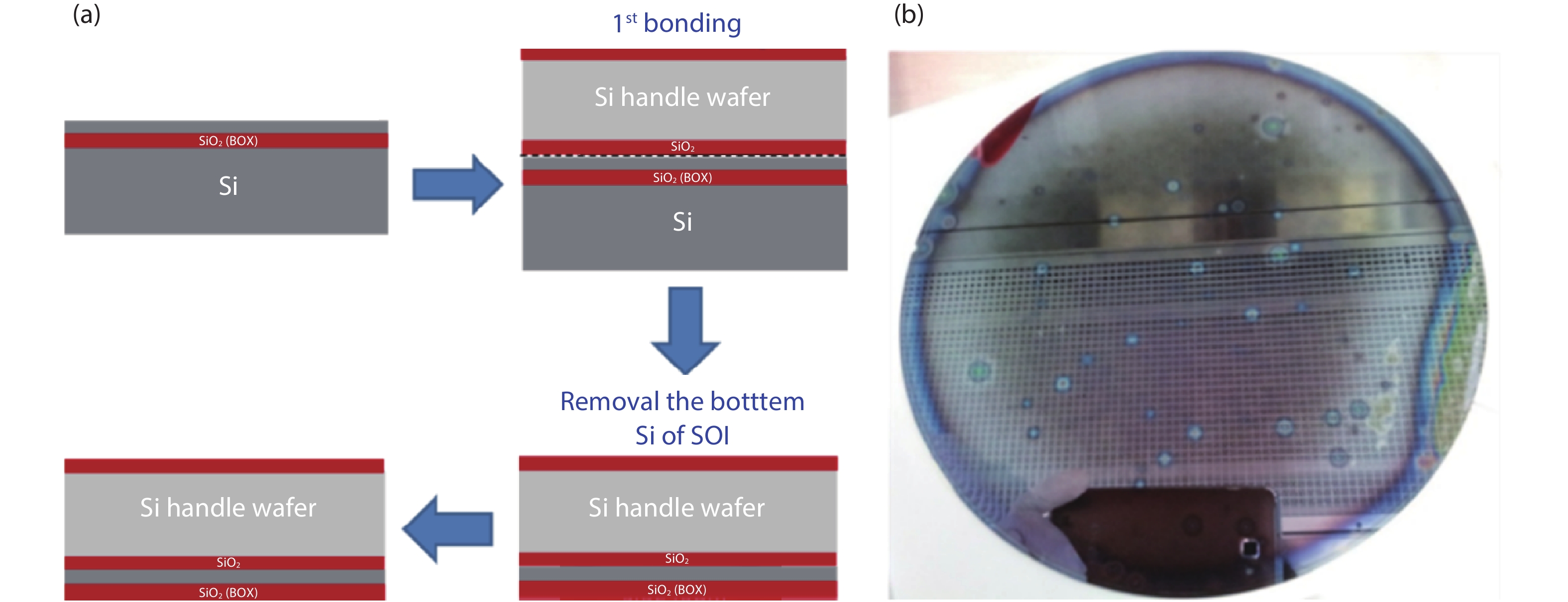
Fig. 1.
Schematic views of (a) silicon–glass anodic bonding and (b) silicon–silicon anodic bonding mediated with a borosilicate glass layer.
REVIEWS
Shuyu Bao1, ‡, , Yue Wang1, ‡, Khaw Lina1, Li Zhang1, Bing Wang1, 2, , Wardhana Aji Sasangka1, Kenneth Eng Kian Lee1, Soo Jin Chua1, 3, Jurgen Michel1, 4, Eugene Fitzgerald1, 5, Chuan Seng Tan1, 6 and Kwang Hong Lee1,
Corresponding author: Shuyu Bao, shuyu@smart.mit.edu; Bing Wang, wangb266@mail.sysu.edu.cn; Kwang Hong Lee, leek0046@e.ntu.edu.sg
Abstract: The heterogeneous integration of III–V devices with Si-CMOS on a common Si platform has shown great promise in the new generations of electrical and optical systems for novel applications, such as HEMT or LED with integrated control circuitry. For heterogeneous integration, direct wafer bonding (DWB) techniques can overcome the materials and thermal mismatch issues by directly bonding dissimilar materials systems and device structures together. In addition, DWB can perform at wafer-level, which eases the requirements for integration alignment and increases the scalability for volume production. In this paper, a brief review of the different bonding technologies is discussed. After that, three main DWB techniques of single-, double- and multi-bonding are presented with the demonstrations of various heterogeneous integration applications. Meanwhile, the integration challenges, such as micro-defects, surface roughness and bonding yield are discussed in detail.
Keywords: material, thin film, integrated circuit
| [1] |
Deleonibus S. Physical and technological limitations of nano CMOS devices to the end of the roadmap and beyond. Eur Phys J Appl Phys, 2006, 36, 197 doi: 10.1051/epjap:2006158
|
| [2] |
Ito T, Okazaki S. Pushing the limits of lithography. Nature, 2000, 406, 1027 doi: 10.1038/35023233
|
| [3] |
Wong H S P, Frank D J, Solomon P M, et al. Nanoscale CMOS. Proc IEEE, 1999, 87, 537 doi: 10.1109/5.752515
|
| [4] |
Kim D H, del Alamo J A. 30 nm E-mode InAs PHEMTs for THz and future logic applications. 2008 IEEE International Electron Devices Meeting, 2008, 1
|
| [5] |
Passlack M, Zurcher P, Rajagopalan K, et al. High mobility III–V MOSFETs for RF and digital applications. 2007 IEEE Int Electron Devices Meet, 2007, 621
|
| [6] |
Kim R H, Kim D H, Xiao J L, et al. Waterproof AlInGaP optoelectronics on stretchable substrates with applications in biomedicine and robotics. Nat Mater, 2010, 9, 929 doi: 10.1038/nmat2879
|
| [7] |
Ko H, Takei K, Kapadia R, et al. Ultrathin compound semiconductor on insulator layers for high-performance nanoscale transistors. Nature, 2010, 468, 286 doi: 10.1038/nature09541
|
| [8] |
Yoon J, Jo S, Chun I S, et al. GaAs photovoltaics and optoelectronics using releasable multilayer epitaxial assemblies. Nature, 2010, 465, 329 doi: 10.1038/nature09054
|
| [9] |
Lin J J, You T G, Jin T T, et al. Wafer-scale heterogeneous integration InP on trenched Si with a bubble-free interface. APL Mater, 2020, 8, 051110 doi: 10.1063/5.0004427
|
| [10] |
Lin J J, You T G, Wang M, et al. Efficient ion-slicing of InP thin film for Si-based hetero-integration. Nanotechnology, 2018, 29, 504002 doi: 10.1088/1361-6528/aae281
|
| [11] |
Lee K H, Bao S, Fitzgerald E, et al. Integration of III–V materials and Si-CMOS through double layer transfer process. 2014 4th IEEE Int Work Low Temp Bond 3D Integr LTB-3D, 2014, 32
|
| [12] |
Lee K H, Bao S Y, Kohen D, et al. Monolithic integration of III–V HEMT and Si-CMOS through TSV-less 3D wafer stacking. 2015 IEEE 65th Electronic Components and Technology Conference (ECTC), 2015, 560
|
| [13] |
Lee K H, Bao S Y, Lee K E K, et al. Integration of 200 mm Si-CMOS and III–V materials through wafer bonding. 2017 5th International Workshop on Low Temperature Bonding for 3D Integration (LTB-3D), 2017, 30
|
| [14] |
Yan Y Q, Huang K, Zhou H Y, et al. Wafer-scale fabrication of 42° rotated Y-cut LiTaO3-on-insulator (LTOI) substrate for a SAW resonator. ACS Appl Electron Mater, 2019, 1, 1660 doi: 10.1021/acsaelm.9b00351
|
| [15] |
Huang K, Jia Q, You T G, et al. Investigation on thermodynamics of ion-slicing of GaN and heterogeneously integrating high-quality GaN films on CMOS compatible Si(100) substrates. Sci Rep, 2017, 7, 15017. doi: 10.1038/s41598-017-15094-1
|
| [16] |
Yi A L, Zheng Y, Huang H, et al. Wafer-scale 4H-silicon carbide-on-insulator (4H-SiCOI) platform for nonlinear integrated optical devices. Opt Mater, 2020, 107, 109990 doi: 10.1016/j.optmat.2020.109990
|
| [17] |
Lei D, Lee K H, Bao S Y, et al. GeSn-on-insulator substrate formed by direct wafer bonding. Appl Phys Lett, 2016, 109, 022106 doi: 10.1063/1.4958844
|
| [18] |
Xu W H, Wang Y, You T G, et al. First demonstration of waferscale heterogeneous integration of Ga2O3 MOSFETs on SiC and Si substrates by ion-cutting process. 2019 IEEE International Electron Devices Meeting (IEDM), 2019, 12.5. 1
|
| [19] |
Gösele U, Tong Q Y. Semiconductor wafer bonding. Annu Rev Mater Sci, 1998, 28, 215 doi: 10.1146/annurev.matsci.28.1.215
|
| [20] |
Tong Q Y, Gösele U. Semiconductor wafer bonding: Recent developments. Mater Chem Phys, 1994, 37, 101 doi: 10.1016/0254-0584(94)90080-9
|
| [21] |
Lasky J B, Stiffler S R, White F R, et al. Silicon-on-insulator (SOI) by bonding and ETCH-back. 1985 Int Electron Devices Meet, 1985, 684
|
| [22] |
Plößl A. Wafer direct bonding: Tailoring adhesion between brittle materials. Mater Sci Eng R, 1999, 25, 1 doi: 10.1016/S0927-796X(98)00017-5
|
| [23] |
Turner K T, Spearing S M. Modeling of direct wafer bonding: Effect of wafer bow and etch patterns. J Appl Phys, 2002, 92, 7658 doi: 10.1063/1.1521792
|
| [24] |
Taniyama S, Wang Y H, Fujino M, et al. Room temperature wafer bonding using surface activated bonding method. 2008 IEEE 9th VLSI Packag Work Jpn, 2008, 141
|
| [25] |
Takagi H, Kikuchi K, Maeda R, et al. Surface activated bonding of silicon wafers at room temperature. Appl Phys Lett, 1996, 68, 2222 doi: 10.1063/1.115865
|
| [26] |
Howlader M M R, Watanabe T, Suga T. Investigation of the bonding strength and interface current of p-Si/n-GaAs wafers bonded by surface activated bonding at room temperature. J Vac Sci Technol B, 2001, 19, 2114 doi: 10.1116/1.1414115
|
| [27] |
Chung T R, Yang L, Hosoda N, et al. Room temperature GaAs–Si and InP–Si wafer direct bonding by the surface activated bonding method. Nucl Instrum Methods Phys Res B, 1997, 121, 203 doi: 10.1016/S0168-583X(96)00546-0
|
| [28] |
Takagi H, Utsumi J, Takahashi M, et al. Room-temperature bonding of oxide wafers by Ar-beam surface activation. ECS Trans, 2019, 16, 531 doi: 10.1149/1.2982908
|
| [29] |
Essig S, Moutanabbir O, Wekkeli A, et al. Fast atom beam-activated n-Si/n-GaAs wafer bonding with high interfacial transparency and electrical conductivity. J Appl Phys, 2013, 113, 203512 doi: 10.1063/1.4807905
|
| [30] |
Hinterreiter A P, Rebhan B, Flötgen C, et al. Surface pretreated low-temperature aluminum-aluminum wafer bonding. Microsyst Technol, 2018, 24, 773 doi: 10.1007/s00542-017-3520-8
|
| [31] |
Suga T, He R, Vakanas G, et al. Direct Cu to Cu bonding and other alternative bonding techniques in 3D packaging. In: 3D Microelectronic Packaging. Cham: Springer International Publishing, 2017, 129
|
| [32] |
Malik N, Schjølberg-Henriksen K, Poppe E, et al. AlAl thermocompression bonding for wafer-level MEMS sealing. Sens Actuators A, 2014, 211, 115 doi: 10.1016/j.sna.2014.02.030
|
| [33] |
Tsau C H, Spearing S M, Schmidt M A. Fabrication of wafer-level thermocompression bonds. J Microelectromechan Syst, 2002, 11, 641 doi: 10.1109/JMEMS.2002.805214
|
| [34] |
Xu D H, Jing E R, Xiong B, et al. Wafer-level vacuum packaging of micromachined thermoelectric IR sensors. IEEE Trans Adv Packag, 2010, 33, 904 doi: 10.1109/TADVP.2010.2072925
|
| [35] |
Fan J, Lim D F, Tan C S. Effects of surface treatment on the bonding quality of wafer-level Cu-to-Cu thermo-compression bonding for 3D integration. J Micromech Microeng, 2013, 23, 045025 doi: 10.1088/0960-1317/23/4/045025
|
| [36] |
Chen K N, Fan A, Reif R. Microstructure examination of copper wafer bonding. J Electron Mater, 2001, 30, 331 doi: 10.1007/s11664-001-0039-6
|
| [37] |
Gao K, Zhang Q Y, Su W G, et al. Patterned Al–Ge wafer bonding for reducing in-process side leakage of eutectic. 2018 IEEE 13th Annual International Conference on Nano/Micro Engineered and Molecular Systems (NEMS), 2018, 332
|
| [38] |
Tang Y S, Chen H C, Kho Y T, et al. Investigation and optimization of ultrathin buffer layers used in Cu/Sn eutectic bonding. IEEE Trans Compon Packag Manuf Technol, 2018, 8, 1225 doi: 10.1109/TCPMT.2018.2838047
|
| [39] |
Wolffenbuttel R F. Low-temperature intermediate Au-Si wafer bonding; eutectic or silicide bond. Sens Actuators A, 1997, 62, 680 doi: 10.1016/S0924-4247(97)01550-1
|
| [40] |
Cheng Y T, Lin L, Najafi K. Localized silicon fusion and eutectic bonding for MEMS fabrication and packaging. J Microelectromechan Syst, 2000, 9, 3 doi: 10.1109/84.825770
|
| [41] |
Quero J M, Perdigones F, Aracil C. Microfabrication technologies used for creating smart devices for industrial applications. In: Smart Sensors and MEMs. Amsterdam: Elsevier, 2018, 291
|
| [42] |
Li D L, Shang Z G, She Y, et al. Investigation of Au/Si eutectic wafer bonding for MEMS accelerometers. Micromachines, 2017, 8, 158 doi: 10.3390/mi8050158
|
| [43] |
Mescheder U M, Alavi M, Hiltmann K, et al. Local laser bonding for low temperature budget. Sens Actuators A, 2002, 97/98, 422 doi: 10.1016/S0924-4247(01)00871-8
|
| [44] |
Knechtel R. Glass frit bonding: An universal technology for wafer level encapsulation and packaging. Microsyst Technol, 2005, 12, 63 doi: 10.1007/s00542-005-0022-x
|
| [45] |
Wu G Q, Xu D H, Xiong B, et al. Wafer-level vacuum packaging for MEMS resonators using glass frit bonding. J Microelectromechan Syst, 2012, 21, 1484 doi: 10.1109/JMEMS.2012.2211572
|
| [46] |
Tian R, Cao F, Li Y, et al. Application of laser-assisted glass frit bonding encapsulation in all inorganic quantum dot light emitting devices. Mol Cryst Liq Cryst, 2018, 676, 59 doi: 10.1080/15421406.2019.1595698
|
| [47] |
Niklaus F, Enoksson P, Kalvesten E, et al. Low-temperature full wafer adhesive bonding. J Micromechan Microeng, 2001, 11, 100 doi: 10.1088/0960-1317/11/2/303
|
| [48] |
Dragoi V, Glinsner T, Mittendorfer G, et al. Adhesive wafer bonding for MEMS applications. Proc SPIE 5116, Smart Sensors, Actuators, and MEMS, 2003, 5116, 160 doi: 10.1117/12.499077
|
| [49] |
Bleiker S J, Dubois V, Schröder S, et al. Adhesive wafer bonding with ultra-thin intermediate polymer layers. Sens Actuators A, 2017, 260, 16 doi: 10.1016/j.sna.2017.04.018
|
| [50] |
Niklaus F, Stemme G, Lu J Q, et al. Adhesive wafer bonding. J Appl Phys, 2006, 99, 031101 doi: 10.1063/1.2168512
|
| [51] |
Niklaus F, Enoksson P, Kälvesten E, et al. A method to maintain wafer alignment precision during adhesive wafer bonding. Sens Actuators A, 2003, 107, 273 doi: 10.1016/S0924-4247(03)00356-X
|
| [52] |
Niklaus F, Kumar R J, McMahon J J, et al. Adhesive wafer bonding using partially cured benzocyclobutene for three-dimensional integration. J Electrochem Soc, 2006, 153, G291 doi: 10.1149/1.2168409
|
| [53] |
Pomerantz D I. Anodic bonding. Google Patents, 1968
|
| [54] |
Henmi H, Shoji S, Shoji Y, et al. Vacuum packaging for microsensors by glass-silicon anodic bonding. Sens Actuators A, 1994, 43, 243 doi: 10.1016/0924-4247(94)80003-0
|
| [55] |
Hanneborg A, Nese M, Ohlckers P. Silicon-to-silicon anodic bonding with a borosilicate glass layer. J Micromech Microeng, 1991, 1, 139 doi: 10.1088/0960-1317/1/3/002
|
| [56] |
Lee T M H, Hsing I M, Liaw C Y N. An improved anodic bonding process using pulsed voltage technique. J Microelectromechan Syst, 2000, 9, 469 doi: 10.1109/84.896767
|
| [57] |
Schmidt M A. Wafer-to-wafer bonding for microstructure formation. Proc IEEE, 1998, 86, 1575 doi: 10.1109/5.704262
|
| [58] |
Tong Q Y, Gösele U. A model of low-temperature wafer bonding and its applications. J Electrochem Soc, 2019, 143, 1773 doi: 10.1149/1.1836715
|
| [59] |
Lee K H, Bao S Y, Wang Y, et al. Suppression of interfacial voids formation during silane (SiH4)-based silicon oxide bonding with a thin silicon nitride capping layer. J Appl Phys, 2018, 123, 015302 doi: 10.1063/1.5001796
|
| [60] |
Bao S, Lee K H, Chong G Y, et al. AlN–AlN layer bonding and its thermal characteristics. ECS J Solid State Sci Technol, 2015, 4, P200 doi: 10.1149/2.0121507jss
|
| [61] |
Bao S Y, Lee K H, Wang C, et al. Germanium-on-insulator virtual substrate for InGaP epitaxy. Mater Sci Semicond Process, 2017, 58, 15 doi: 10.1016/j.mssp.2016.11.001
|
| [62] |
Lee K H, Bao S Y, Chong G Y, et al. Fabrication and characterization of germanium-on-insulator through epitaxy, bonding, and layer transfer. J Appl Phys, 2014, 116, 103506 doi: 10.1063/1.4895487
|
| [63] |
Lee K H, Bao S Y, Chong G Y, et al. Fabrication of germanium-on-insulator (GOI) with improved threading dislocation density (TDD) via buffer-less epitaxy and bonding. 2014 7th Int Silicon-Ger Technol Device Meet ISTDM, 2014, 51
|
| [64] |
Lee K H, Bao S Y, Chong G Y, et al. Defects reduction of Ge epitaxial film in a germanium-on-insulator wafer by annealing in oxygen ambient. APL Mater, 2015, 3, 016102 doi: 10.1063/1.4905487
|
| [65] |
Lee K H, Tan C S, Wang Y, et al. Monolithic integration of Si-CMOS and III–V-on-Si through direct wafer bonding process. IEEE J Electron Devices Soc, 2018, 6, 571 doi: 10.1109/JEDS.2017.2787202
|
| [66] |
Lee K H, Zhang L, Wang B, et al. Integration of Si-CMOS and III–V materials through multi-wafer stacking. 2017 IEEE SOI-3D-Subthreshold Microelectronics Technology Unified Conference (S3S), 2017, 1
|
| [67] |
Lee K H, Wang Y, Zhang L, et al. GaN LED on quartz substrate through wafer bonding and layer transfer processes. ECS Trans, 2018, 86, 31 doi: 10.1149/08605.0031ecst
|
| [68] |
Lee K H, Zhang L, Wang Y, et al. High bonding yield and brighter integrated GaN LED and Si-CMOS. 2019 6th International Workshop on Low Temperature Bonding for 3D Integration (LTB-3D), 2019, 33
|
| [69] |
Lee K H, Bao S Y, Zhang L, et al. Integration of GaAs, GaN, and Si-CMOS on a common 200 mm Si substrate through multilayer transfer process. Appl Phys Express, 2016, 9, 086501 doi: 10.7567/APEX.9.086501
|


Article views: 17453 Times PDF downloads: 2030 Times Cited by: 0 Times
Received: 18 May 2020 Revised: 18 June 2020 Online: Accepted Manuscript: 04 September 2020Uncorrected proof: 11 September 2020Published: 08 February 2021
| Citation: |
Shuyu Bao, Yue Wang, Khaw Lina, Li Zhang, Bing Wang, Wardhana Aji Sasangka, Kenneth Eng Kian Lee, Soo Jin Chua, Jurgen Michel, Eugene Fitzgerald, Chuan Seng Tan, Kwang Hong Lee. A review of silicon-based wafer bonding processes, an approach to realize the monolithic integration of Si-CMOS and III–V-on-Si wafers[J]. Journal of Semiconductors, 2021, 42(2): 023106. doi: 10.1088/1674-4926/42/2/023106
****
S Y Bao, Y Wang, K Lina, L Zhang, B Wang, W A Sasangka, K E K Lee, S J Chua, J Michel, E Fitzgerald, C S Tan, K H Lee, A review of silicon-based wafer bonding processes, an approach to realize the monolithic integration of Si-CMOS and III–V-on-Si wafers[J]. J. Semicond., 2021, 42(2): 023106. doi: 10.1088/1674-4926/42/2/023106.

|
| [1] |
Deleonibus S. Physical and technological limitations of nano CMOS devices to the end of the roadmap and beyond. Eur Phys J Appl Phys, 2006, 36, 197 doi: 10.1051/epjap:2006158
|
| [2] |
Ito T, Okazaki S. Pushing the limits of lithography. Nature, 2000, 406, 1027 doi: 10.1038/35023233
|
| [3] |
Wong H S P, Frank D J, Solomon P M, et al. Nanoscale CMOS. Proc IEEE, 1999, 87, 537 doi: 10.1109/5.752515
|
| [4] |
Kim D H, del Alamo J A. 30 nm E-mode InAs PHEMTs for THz and future logic applications. 2008 IEEE International Electron Devices Meeting, 2008, 1
|
| [5] |
Passlack M, Zurcher P, Rajagopalan K, et al. High mobility III–V MOSFETs for RF and digital applications. 2007 IEEE Int Electron Devices Meet, 2007, 621
|
| [6] |
Kim R H, Kim D H, Xiao J L, et al. Waterproof AlInGaP optoelectronics on stretchable substrates with applications in biomedicine and robotics. Nat Mater, 2010, 9, 929 doi: 10.1038/nmat2879
|
| [7] |
Ko H, Takei K, Kapadia R, et al. Ultrathin compound semiconductor on insulator layers for high-performance nanoscale transistors. Nature, 2010, 468, 286 doi: 10.1038/nature09541
|
| [8] |
Yoon J, Jo S, Chun I S, et al. GaAs photovoltaics and optoelectronics using releasable multilayer epitaxial assemblies. Nature, 2010, 465, 329 doi: 10.1038/nature09054
|
| [9] |
Lin J J, You T G, Jin T T, et al. Wafer-scale heterogeneous integration InP on trenched Si with a bubble-free interface. APL Mater, 2020, 8, 051110 doi: 10.1063/5.0004427
|
| [10] |
Lin J J, You T G, Wang M, et al. Efficient ion-slicing of InP thin film for Si-based hetero-integration. Nanotechnology, 2018, 29, 504002 doi: 10.1088/1361-6528/aae281
|
| [11] |
Lee K H, Bao S, Fitzgerald E, et al. Integration of III–V materials and Si-CMOS through double layer transfer process. 2014 4th IEEE Int Work Low Temp Bond 3D Integr LTB-3D, 2014, 32
|
| [12] |
Lee K H, Bao S Y, Kohen D, et al. Monolithic integration of III–V HEMT and Si-CMOS through TSV-less 3D wafer stacking. 2015 IEEE 65th Electronic Components and Technology Conference (ECTC), 2015, 560
|
| [13] |
Lee K H, Bao S Y, Lee K E K, et al. Integration of 200 mm Si-CMOS and III–V materials through wafer bonding. 2017 5th International Workshop on Low Temperature Bonding for 3D Integration (LTB-3D), 2017, 30
|
| [14] |
Yan Y Q, Huang K, Zhou H Y, et al. Wafer-scale fabrication of 42° rotated Y-cut LiTaO3-on-insulator (LTOI) substrate for a SAW resonator. ACS Appl Electron Mater, 2019, 1, 1660 doi: 10.1021/acsaelm.9b00351
|
| [15] |
Huang K, Jia Q, You T G, et al. Investigation on thermodynamics of ion-slicing of GaN and heterogeneously integrating high-quality GaN films on CMOS compatible Si(100) substrates. Sci Rep, 2017, 7, 15017. doi: 10.1038/s41598-017-15094-1
|
| [16] |
Yi A L, Zheng Y, Huang H, et al. Wafer-scale 4H-silicon carbide-on-insulator (4H-SiCOI) platform for nonlinear integrated optical devices. Opt Mater, 2020, 107, 109990 doi: 10.1016/j.optmat.2020.109990
|
| [17] |
Lei D, Lee K H, Bao S Y, et al. GeSn-on-insulator substrate formed by direct wafer bonding. Appl Phys Lett, 2016, 109, 022106 doi: 10.1063/1.4958844
|
| [18] |
Xu W H, Wang Y, You T G, et al. First demonstration of waferscale heterogeneous integration of Ga2O3 MOSFETs on SiC and Si substrates by ion-cutting process. 2019 IEEE International Electron Devices Meeting (IEDM), 2019, 12.5. 1
|
| [19] |
Gösele U, Tong Q Y. Semiconductor wafer bonding. Annu Rev Mater Sci, 1998, 28, 215 doi: 10.1146/annurev.matsci.28.1.215
|
| [20] |
Tong Q Y, Gösele U. Semiconductor wafer bonding: Recent developments. Mater Chem Phys, 1994, 37, 101 doi: 10.1016/0254-0584(94)90080-9
|
| [21] |
Lasky J B, Stiffler S R, White F R, et al. Silicon-on-insulator (SOI) by bonding and ETCH-back. 1985 Int Electron Devices Meet, 1985, 684
|
| [22] |
Plößl A. Wafer direct bonding: Tailoring adhesion between brittle materials. Mater Sci Eng R, 1999, 25, 1 doi: 10.1016/S0927-796X(98)00017-5
|
| [23] |
Turner K T, Spearing S M. Modeling of direct wafer bonding: Effect of wafer bow and etch patterns. J Appl Phys, 2002, 92, 7658 doi: 10.1063/1.1521792
|
| [24] |
Taniyama S, Wang Y H, Fujino M, et al. Room temperature wafer bonding using surface activated bonding method. 2008 IEEE 9th VLSI Packag Work Jpn, 2008, 141
|
| [25] |
Takagi H, Kikuchi K, Maeda R, et al. Surface activated bonding of silicon wafers at room temperature. Appl Phys Lett, 1996, 68, 2222 doi: 10.1063/1.115865
|
| [26] |
Howlader M M R, Watanabe T, Suga T. Investigation of the bonding strength and interface current of p-Si/n-GaAs wafers bonded by surface activated bonding at room temperature. J Vac Sci Technol B, 2001, 19, 2114 doi: 10.1116/1.1414115
|
| [27] |
Chung T R, Yang L, Hosoda N, et al. Room temperature GaAs–Si and InP–Si wafer direct bonding by the surface activated bonding method. Nucl Instrum Methods Phys Res B, 1997, 121, 203 doi: 10.1016/S0168-583X(96)00546-0
|
| [28] |
Takagi H, Utsumi J, Takahashi M, et al. Room-temperature bonding of oxide wafers by Ar-beam surface activation. ECS Trans, 2019, 16, 531 doi: 10.1149/1.2982908
|
| [29] |
Essig S, Moutanabbir O, Wekkeli A, et al. Fast atom beam-activated n-Si/n-GaAs wafer bonding with high interfacial transparency and electrical conductivity. J Appl Phys, 2013, 113, 203512 doi: 10.1063/1.4807905
|
| [30] |
Hinterreiter A P, Rebhan B, Flötgen C, et al. Surface pretreated low-temperature aluminum-aluminum wafer bonding. Microsyst Technol, 2018, 24, 773 doi: 10.1007/s00542-017-3520-8
|
| [31] |
Suga T, He R, Vakanas G, et al. Direct Cu to Cu bonding and other alternative bonding techniques in 3D packaging. In: 3D Microelectronic Packaging. Cham: Springer International Publishing, 2017, 129
|
| [32] |
Malik N, Schjølberg-Henriksen K, Poppe E, et al. AlAl thermocompression bonding for wafer-level MEMS sealing. Sens Actuators A, 2014, 211, 115 doi: 10.1016/j.sna.2014.02.030
|
| [33] |
Tsau C H, Spearing S M, Schmidt M A. Fabrication of wafer-level thermocompression bonds. J Microelectromechan Syst, 2002, 11, 641 doi: 10.1109/JMEMS.2002.805214
|
| [34] |
Xu D H, Jing E R, Xiong B, et al. Wafer-level vacuum packaging of micromachined thermoelectric IR sensors. IEEE Trans Adv Packag, 2010, 33, 904 doi: 10.1109/TADVP.2010.2072925
|
| [35] |
Fan J, Lim D F, Tan C S. Effects of surface treatment on the bonding quality of wafer-level Cu-to-Cu thermo-compression bonding for 3D integration. J Micromech Microeng, 2013, 23, 045025 doi: 10.1088/0960-1317/23/4/045025
|
| [36] |
Chen K N, Fan A, Reif R. Microstructure examination of copper wafer bonding. J Electron Mater, 2001, 30, 331 doi: 10.1007/s11664-001-0039-6
|
| [37] |
Gao K, Zhang Q Y, Su W G, et al. Patterned Al–Ge wafer bonding for reducing in-process side leakage of eutectic. 2018 IEEE 13th Annual International Conference on Nano/Micro Engineered and Molecular Systems (NEMS), 2018, 332
|
| [38] |
Tang Y S, Chen H C, Kho Y T, et al. Investigation and optimization of ultrathin buffer layers used in Cu/Sn eutectic bonding. IEEE Trans Compon Packag Manuf Technol, 2018, 8, 1225 doi: 10.1109/TCPMT.2018.2838047
|
| [39] |
Wolffenbuttel R F. Low-temperature intermediate Au-Si wafer bonding; eutectic or silicide bond. Sens Actuators A, 1997, 62, 680 doi: 10.1016/S0924-4247(97)01550-1
|
| [40] |
Cheng Y T, Lin L, Najafi K. Localized silicon fusion and eutectic bonding for MEMS fabrication and packaging. J Microelectromechan Syst, 2000, 9, 3 doi: 10.1109/84.825770
|
| [41] |
Quero J M, Perdigones F, Aracil C. Microfabrication technologies used for creating smart devices for industrial applications. In: Smart Sensors and MEMs. Amsterdam: Elsevier, 2018, 291
|
| [42] |
Li D L, Shang Z G, She Y, et al. Investigation of Au/Si eutectic wafer bonding for MEMS accelerometers. Micromachines, 2017, 8, 158 doi: 10.3390/mi8050158
|
| [43] |
Mescheder U M, Alavi M, Hiltmann K, et al. Local laser bonding for low temperature budget. Sens Actuators A, 2002, 97/98, 422 doi: 10.1016/S0924-4247(01)00871-8
|
| [44] |
Knechtel R. Glass frit bonding: An universal technology for wafer level encapsulation and packaging. Microsyst Technol, 2005, 12, 63 doi: 10.1007/s00542-005-0022-x
|
| [45] |
Wu G Q, Xu D H, Xiong B, et al. Wafer-level vacuum packaging for MEMS resonators using glass frit bonding. J Microelectromechan Syst, 2012, 21, 1484 doi: 10.1109/JMEMS.2012.2211572
|
| [46] |
Tian R, Cao F, Li Y, et al. Application of laser-assisted glass frit bonding encapsulation in all inorganic quantum dot light emitting devices. Mol Cryst Liq Cryst, 2018, 676, 59 doi: 10.1080/15421406.2019.1595698
|
| [47] |
Niklaus F, Enoksson P, Kalvesten E, et al. Low-temperature full wafer adhesive bonding. J Micromechan Microeng, 2001, 11, 100 doi: 10.1088/0960-1317/11/2/303
|
| [48] |
Dragoi V, Glinsner T, Mittendorfer G, et al. Adhesive wafer bonding for MEMS applications. Proc SPIE 5116, Smart Sensors, Actuators, and MEMS, 2003, 5116, 160 doi: 10.1117/12.499077
|
| [49] |
Bleiker S J, Dubois V, Schröder S, et al. Adhesive wafer bonding with ultra-thin intermediate polymer layers. Sens Actuators A, 2017, 260, 16 doi: 10.1016/j.sna.2017.04.018
|
| [50] |
Niklaus F, Stemme G, Lu J Q, et al. Adhesive wafer bonding. J Appl Phys, 2006, 99, 031101 doi: 10.1063/1.2168512
|
| [51] |
Niklaus F, Enoksson P, Kälvesten E, et al. A method to maintain wafer alignment precision during adhesive wafer bonding. Sens Actuators A, 2003, 107, 273 doi: 10.1016/S0924-4247(03)00356-X
|
| [52] |
Niklaus F, Kumar R J, McMahon J J, et al. Adhesive wafer bonding using partially cured benzocyclobutene for three-dimensional integration. J Electrochem Soc, 2006, 153, G291 doi: 10.1149/1.2168409
|
| [53] |
Pomerantz D I. Anodic bonding. Google Patents, 1968
|
| [54] |
Henmi H, Shoji S, Shoji Y, et al. Vacuum packaging for microsensors by glass-silicon anodic bonding. Sens Actuators A, 1994, 43, 243 doi: 10.1016/0924-4247(94)80003-0
|
| [55] |
Hanneborg A, Nese M, Ohlckers P. Silicon-to-silicon anodic bonding with a borosilicate glass layer. J Micromech Microeng, 1991, 1, 139 doi: 10.1088/0960-1317/1/3/002
|
| [56] |
Lee T M H, Hsing I M, Liaw C Y N. An improved anodic bonding process using pulsed voltage technique. J Microelectromechan Syst, 2000, 9, 469 doi: 10.1109/84.896767
|
| [57] |
Schmidt M A. Wafer-to-wafer bonding for microstructure formation. Proc IEEE, 1998, 86, 1575 doi: 10.1109/5.704262
|
| [58] |
Tong Q Y, Gösele U. A model of low-temperature wafer bonding and its applications. J Electrochem Soc, 2019, 143, 1773 doi: 10.1149/1.1836715
|
| [59] |
Lee K H, Bao S Y, Wang Y, et al. Suppression of interfacial voids formation during silane (SiH4)-based silicon oxide bonding with a thin silicon nitride capping layer. J Appl Phys, 2018, 123, 015302 doi: 10.1063/1.5001796
|
| [60] |
Bao S, Lee K H, Chong G Y, et al. AlN–AlN layer bonding and its thermal characteristics. ECS J Solid State Sci Technol, 2015, 4, P200 doi: 10.1149/2.0121507jss
|
| [61] |
Bao S Y, Lee K H, Wang C, et al. Germanium-on-insulator virtual substrate for InGaP epitaxy. Mater Sci Semicond Process, 2017, 58, 15 doi: 10.1016/j.mssp.2016.11.001
|
| [62] |
Lee K H, Bao S Y, Chong G Y, et al. Fabrication and characterization of germanium-on-insulator through epitaxy, bonding, and layer transfer. J Appl Phys, 2014, 116, 103506 doi: 10.1063/1.4895487
|
| [63] |
Lee K H, Bao S Y, Chong G Y, et al. Fabrication of germanium-on-insulator (GOI) with improved threading dislocation density (TDD) via buffer-less epitaxy and bonding. 2014 7th Int Silicon-Ger Technol Device Meet ISTDM, 2014, 51
|
| [64] |
Lee K H, Bao S Y, Chong G Y, et al. Defects reduction of Ge epitaxial film in a germanium-on-insulator wafer by annealing in oxygen ambient. APL Mater, 2015, 3, 016102 doi: 10.1063/1.4905487
|
| [65] |
Lee K H, Tan C S, Wang Y, et al. Monolithic integration of Si-CMOS and III–V-on-Si through direct wafer bonding process. IEEE J Electron Devices Soc, 2018, 6, 571 doi: 10.1109/JEDS.2017.2787202
|
| [66] |
Lee K H, Zhang L, Wang B, et al. Integration of Si-CMOS and III–V materials through multi-wafer stacking. 2017 IEEE SOI-3D-Subthreshold Microelectronics Technology Unified Conference (S3S), 2017, 1
|
| [67] |
Lee K H, Wang Y, Zhang L, et al. GaN LED on quartz substrate through wafer bonding and layer transfer processes. ECS Trans, 2018, 86, 31 doi: 10.1149/08605.0031ecst
|
| [68] |
Lee K H, Zhang L, Wang Y, et al. High bonding yield and brighter integrated GaN LED and Si-CMOS. 2019 6th International Workshop on Low Temperature Bonding for 3D Integration (LTB-3D), 2019, 33
|
| [69] |
Lee K H, Bao S Y, Zhang L, et al. Integration of GaAs, GaN, and Si-CMOS on a common 200 mm Si substrate through multilayer transfer process. Appl Phys Express, 2016, 9, 086501 doi: 10.7567/APEX.9.086501
|

 WeChat ID
Journal of Semiconductors © 2017 All Rights Reserved 京ICP备05085259号-2

 DownLoad: