SEMICONDUCTOR DEVICES

Fabrication, electrical and photovoltaic characteristics of CuInGeSe4/n-Si diode

I. M. El Radaf1, A. M. Mansour2, and G. B. Sakr3

+ Author Affiliations

 Corresponding author: A. M. Mansour, email: amamansour@gmail.com

PDF

Turn off MathJax

Abstract: The CuInGeSe4 thin film was deposited onto n-type single crystal silicon wafers by the electron beam deposition technique. The Au/CuInGeSe4/n-Si/Al heterojunction device has been fabricated. The structure of the CuInGeSe4 thin film was characterized by X-ray diffraction (XRD), scanning electron microscope (SEM), and energy dispersive X-ray analysis (EDX). The dark current–voltage characteristics of the Au/CuInGeSe4/n-Si/Al heterojunction diode have been studied at a temperature range of 303–383 K. Also, the photovoltaic properties were examined at different illumination intensities. The capacitance–voltage characteristics of the CuInGeSe4/n-Si heterojunction were studied at different temperatures in the dark.

Key words: CuInGeSe4electron beam depositionseries resistance, rectificationideality factor


[1]
Matsushita H, Katsui A. Materials design for Cu-based quaternary compounds derived from chalcopyrite-rule. J Phys Chem Solids, 2005, 66: 1933 doi: 10.1016/j.jpcs.2005.09.028
[2]
Gorgut G P, Fedorchuk A O, Kityk I V, et al. Synthesis and structural properties of CuInGeS4. J Cryst Growth, 2011, 324: 212 doi: 10.1016/j.jcrysgro.2011.02.029
[3]
Li W, Yan X, Xu W L, et al. Efficiency improvement of CIGS solar cells by a modified rear contact. Sol Energy, 2017, 157: 486 doi: 10.1016/j.solener.2017.08.054
[4]
Shah A V, Schade H, Vanecek M, et al. Thin-film silicon solar cell technology. Prog Photovoltaics Res Appl, 2004, 12: 113 doi: 10.1002/pip.533
[5]
Matsushita H, Ochiai T, Mikajiri K, et al. Preparation of CuInGeSe4 thin films by selenization method using the Cu–In–Ge evaporated layer precursors. J Phys Chem Solids, 2005, 66: 1937 doi: 10.1016/j.jpcs.2005.09.031
[6]
Matsushita H, Maeda T, Katsui A, et al. Thermal analysis and synthesis from the melts of Cu-based quaternary compounds Cu–III–IV–VI4 and Cu2–II–IV–VI4(II = Zn, Cd; III = Ga, In; IV = Ge, Sn; VI = Se). J Cryst Growth, 2000, 208: 416 doi: 10.1016/S0022-0248(99)00468-6
[7]
Hughes O H, Woolley J C, Lopez-Rivera S A, et al. Quaternary adamantine selenides and tellurides of the form I III IV VI4. Solid State Commun, 1980, 35: 573 doi: 10.1016/0038-1098(80)90585-2
[8]
Contreras M A, Ramanathan K, Abushama J, et al. Diode characteristics in state-of-the-art ZnO/CdS/ Cu(In1-xGax)Se2 solar cells. Prog Photovolt Res Appl, 2005, 13: 209 doi: 10.1002/pip.626
[9]
Abd El-Rahman K F, Darwish A A A, El-Shazly E A A. Electrical and photovoltaic properties of SnSe/Si heterojunction. Mater Sci Semicond Process, 2014, 25: 123 doi: 10.1016/j.mssp.2013.10.003
[10]
Lin Y, Chen X. Advanced nano deposition methods. Weinheim: Wiley-VCH Verlag GmbH & Co. KGaA, 2016
[11]
Cuomo J J, Rossnagel S M, Haufman H R, et al. Handbook of ion beam processing technology: principles, deposition, film modification, and synthesis. Westwood: Noyes Publications, 1989
[12]
Cividjian N, Hagen C W. Electron-beam-induced nanometer-scale deposition. Adv Imaging Electron Phys, 2006, 143: 1 doi: 10.1016/S1076-5670(06)43001-9
[13]
Strehl P. Beam Instrumentation and Diagnostics. Berlin: Springer, 2006
[14]
El Radaf I M, Nasr M, Mansour A M. Structural, electrical and photovoltaic properties of CoS/Si heterojunction prepared by spray pyrolysis. Mater Res Express, 2018, 5: 015904 doi: 10.1088/2053-1591/aaa25e
[15]
Hassan N, Mansour A M, Roushdy N, et al. Optical sensing performance characteristics of Schottky devices diodes based nano-particle disodium 6-hydroxy-5-[(2-methoxy-5-methyl-4-sulfophenyl)azo]-2-naphthalenesulfonate thin films: A comparison study. Optik (Stuttg), 2018, 158: 1255 doi: 10.1016/j.ijleo.2017.12.203
[16]
Nasr M, El Radaf I M, Mansour A M. Current transport and capacitance–voltage characteristics of an n-PbTe/p-GaP heterojunction prepared using the electron beam deposition technique. J Phys Chem Solids, 2018, 115: 283 doi: 10.1016/j.jpcs.2017.12.029
[17]
Farag A A M, Terra F S, Mahmoud G M, et al. Study of Gaussian distribution of inhomogeneous barrier height for n-InSb/p-GaAs heterojunction prepared by flash evaporation. J Alloys Compd, 2009, 481: 427 doi: 10.1016/j.jallcom.2009.03.004
[18]
Farag A A M, Soliman H S, Atta A A. Analysis of dark and photovoltaic characteristics of Au/Pyronine G(Y)/p-Si/Al heterojunction. Synth Met, 2012, 161: 2759 doi: 10.1016/j.synthmet.2011.10.017
[19]
Farag A A M, Terra F S, Fahim G M M, et al. Current transport and capacitance-voltage characteristics of n-InSb/p-GaP prepared by flash evaporation and liquid phase epitaxy. Met Mater Int, 2012, 18: 509 doi: 10.1007/s12540-012-3020-4
[20]
Gupta R K, Aydın M E, Yakuphanoglu F. Photoconducting and electrical properties of Al/TIPS-pentacene/p-Si/Al hybrid diode for optical sensor applications. Synth Met, 2011, 161: 2355 doi: 10.1016/j.synthmet.2011.09.002
[21]
Yahia I S, Farag A A M, Yakuphanoglu F, et al. Temperature dependence of electronic parameters of organic Schottky diode based on fluorescein sodium salt. Synth Met, 2011, 161: 881 doi: 10.1016/j.synthmet.2011.02.016
[22]
Yahia I S, Fadel M, Sakr G B, et al. Analysis of current–voltage characteristics of Al/p-ZnGa2Se4/n-Si nanocrystalline heterojunction diode. J Alloys Compd, 2011, 509: 4414 doi: 10.1016/j.jallcom.2011.01.068
[23]
Soliman H S, Farag A A M, Khosifan N M, et al. Electronic and photovoltaic properties of Au/pyronine G(Y)/p-GaAs/Au:Zn heterojunction. J Alloys Compd, 2012, 530: 157 doi: 10.1016/j.jallcom.2012.03.053
[24]
Çetinkaya H G, Tecimer H, Uslu H, et al. Photovoltaic characteristics of Au/PVA (Bi-doped)/n-Si Schottky barrier diodes (SBDs) at various temperatures. Curr Appl Phys, 2013, 13: 1150 doi: 10.1016/j.cap.2013.03.010
[25]
Farag A A M, Terra F S, Ashery A, et al. Structural and electrical characteristics of n-InSb/p-GaAs heterojunction prepared by liquid phase epitaxy. J Alloys Compd, 2014, 615: 604 doi: 10.1016/j.jallcom.2014.06.058
[26]
Farag A A M, Terra F S, Ashery A, et al. Structural and electrical characterization of n-InAs/p-GaP heterojunctions prepared by vacuum flash evaporation and liquid phase epitaxy. Optoelectron. Adv Mater – RAPID Commun, 2017, 11: 82
[27]
Ahmad Z, Sayyad M H, Yaseen M, et al. Investigation of 5,10,15,20-Tetrakis(3-,5--Di-Tert-Butylphenyl)Porphyrinatocopper(II) for Electronics Applications. Int J Chem Mol Nucl Mater Metall Eng, 2011, 5: 380
[28]
Farag A A M, Terra F S, Ashery A, et al. Temperature dependence of J-V and C-V characteristics of n-InAs/p-GaAs heterojunctions prepared by flash evaporation technique and liquid phase epitaxy. Indian Pure Appl Phys, 2018, 56: 203
[29]
El-Nahass M M, Metwally H S, El-Sayed H E A , et al. Electrical and photovoltaic properties of FeTPPCl/p-Si heterojunction. Synth Met, 2011, 161: 2253 doi: 10.1016/j.synthmet.2011.08.030
[30]
Hameed T A, El Radaf I M, Elsayed-Ali H E. Characterization of CuInGeSe4 thin films and Al/n-Si/p-CuInGeSe4/Au heterojunction device. J Mater Sci Mater Electron, 2018, 29: 12584 doi: 10.1007/s10854-018-9375-7
[31]
Sze S M, Ng K K. Physics of semiconductor devices. New York: Wiley-Interscience, 2007
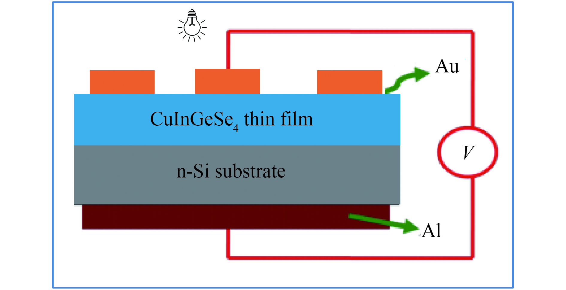
Fig. 1.  (Color online) Schematic diagram of Au/CuInGeSe4/Al heterojunction device.

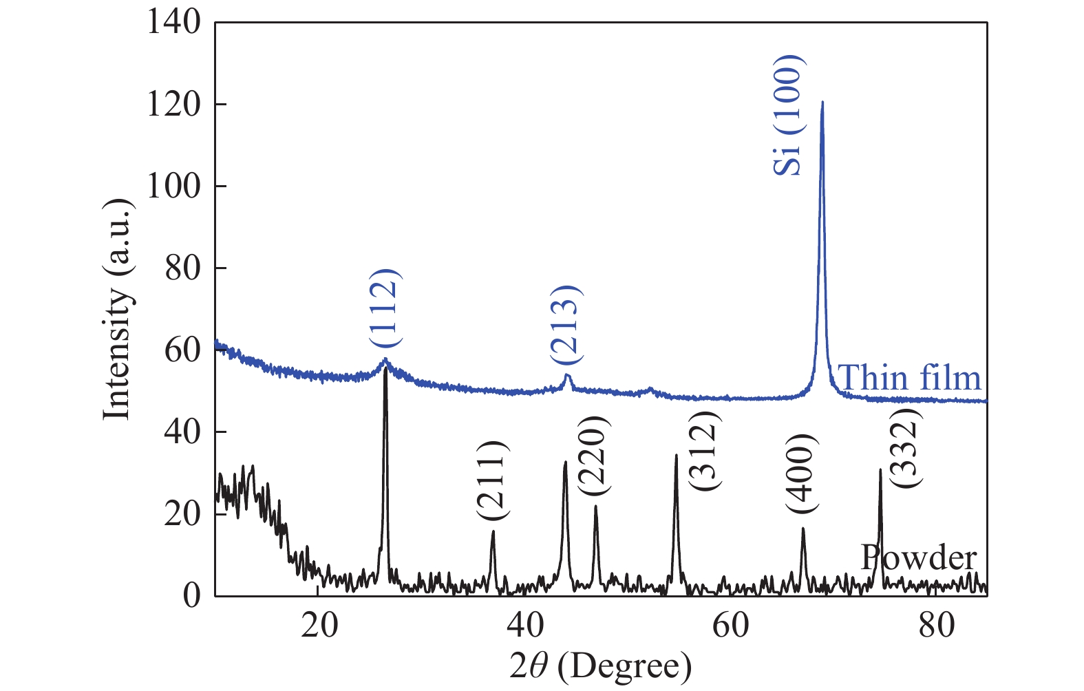
Fig. 2.  (Color online) X-ray diffraction patterns of the CuInGeSe4 thin film deposited onto n-Si substrate.

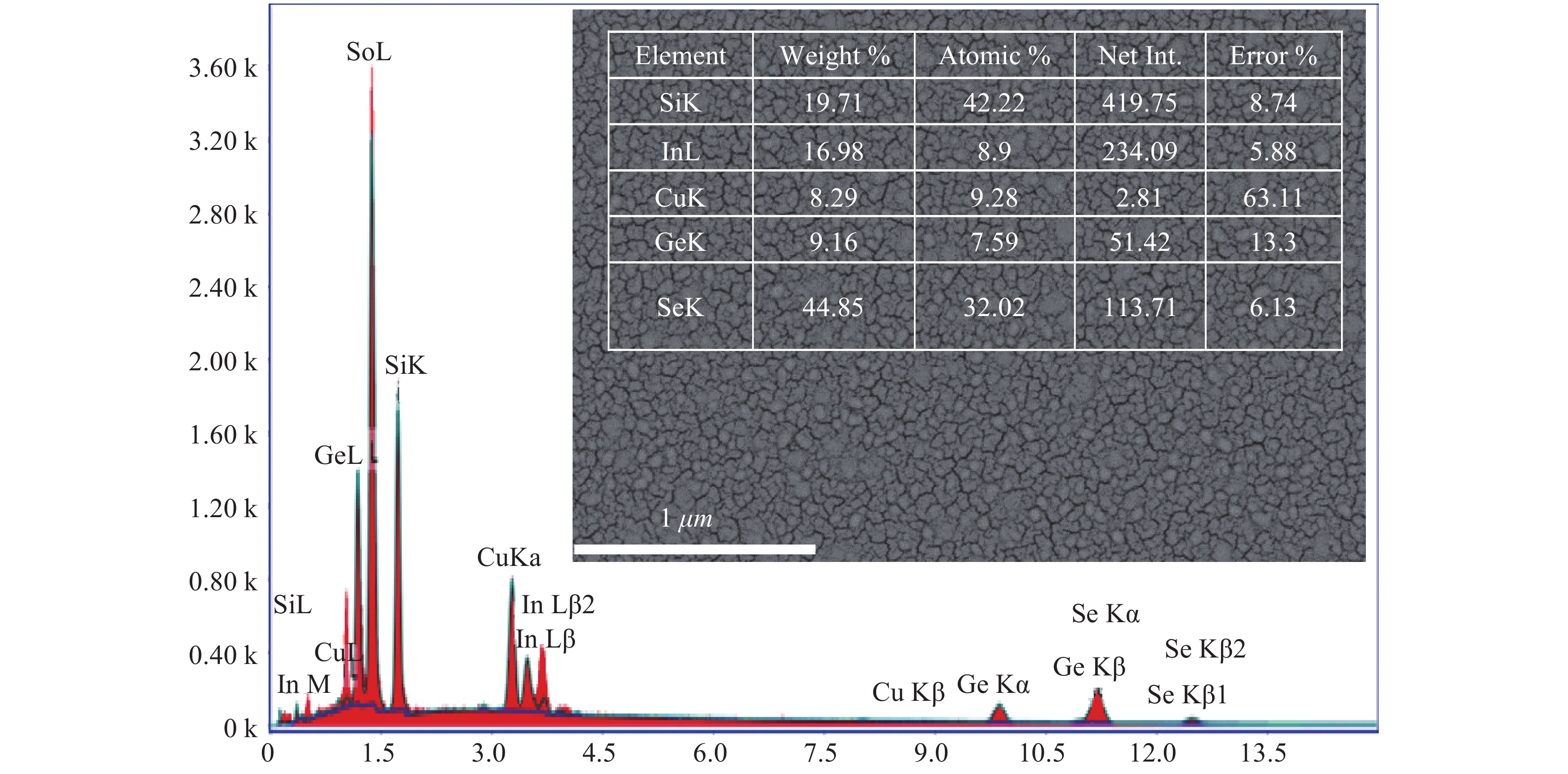
Fig. 3.  (Color online) The scanning electron microscope (SEM) micrograph and EDX of the CuInGeSe4 thin film deposited onto n-Si substrate.

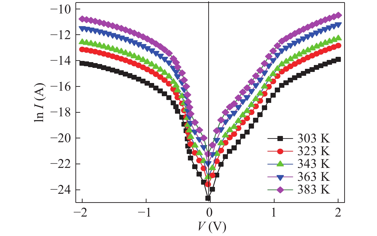
Fig. 4.  (Color online) I–V characteristics of the Au/CuInGeSe4/n-Si/Al device at different temperature in the dark

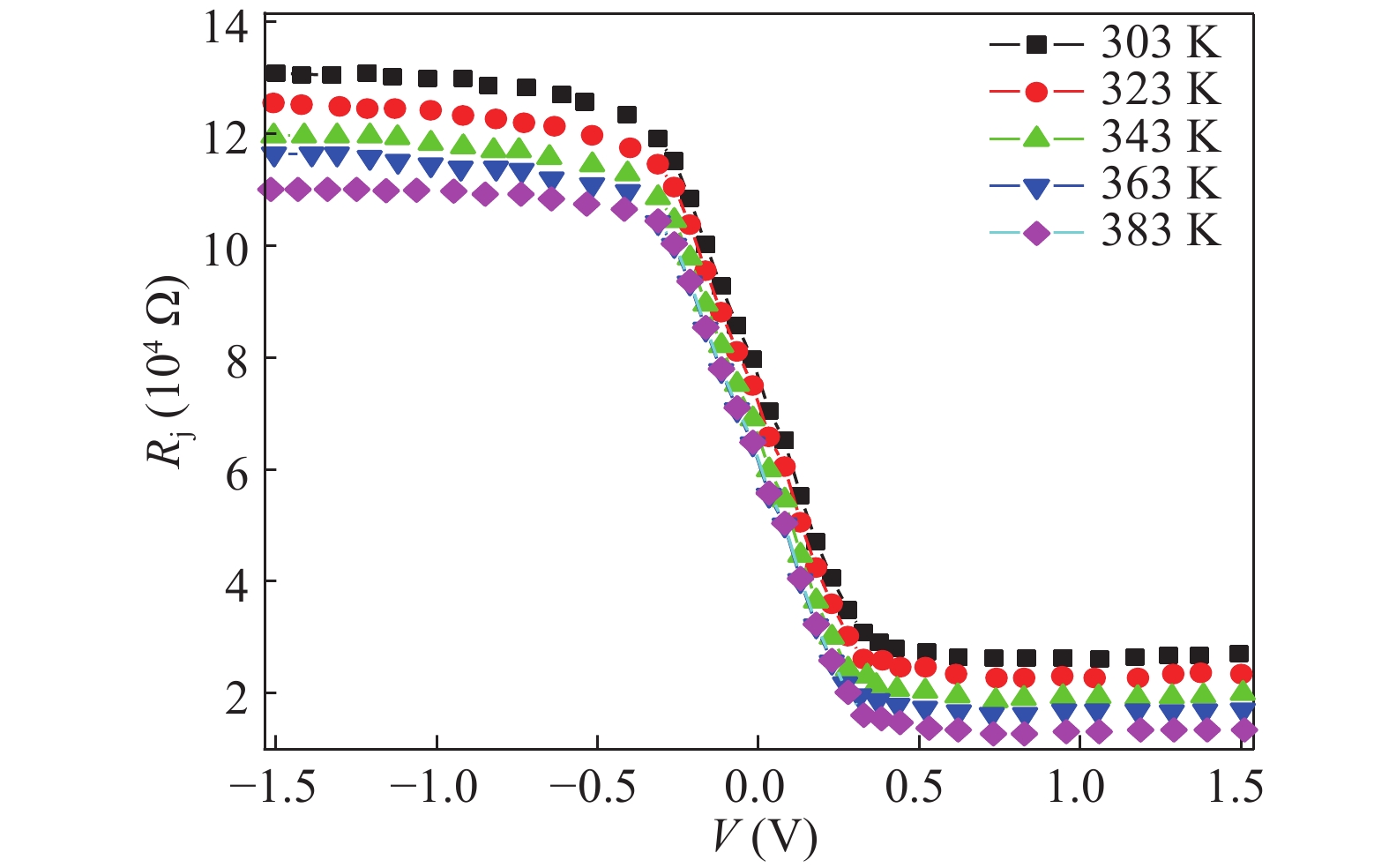
Fig. 5.  (Color online) Junction resistance (Rj) versus V for Au/CuInGeSe4/n-Si/Al heterojunction device at different temperatures.

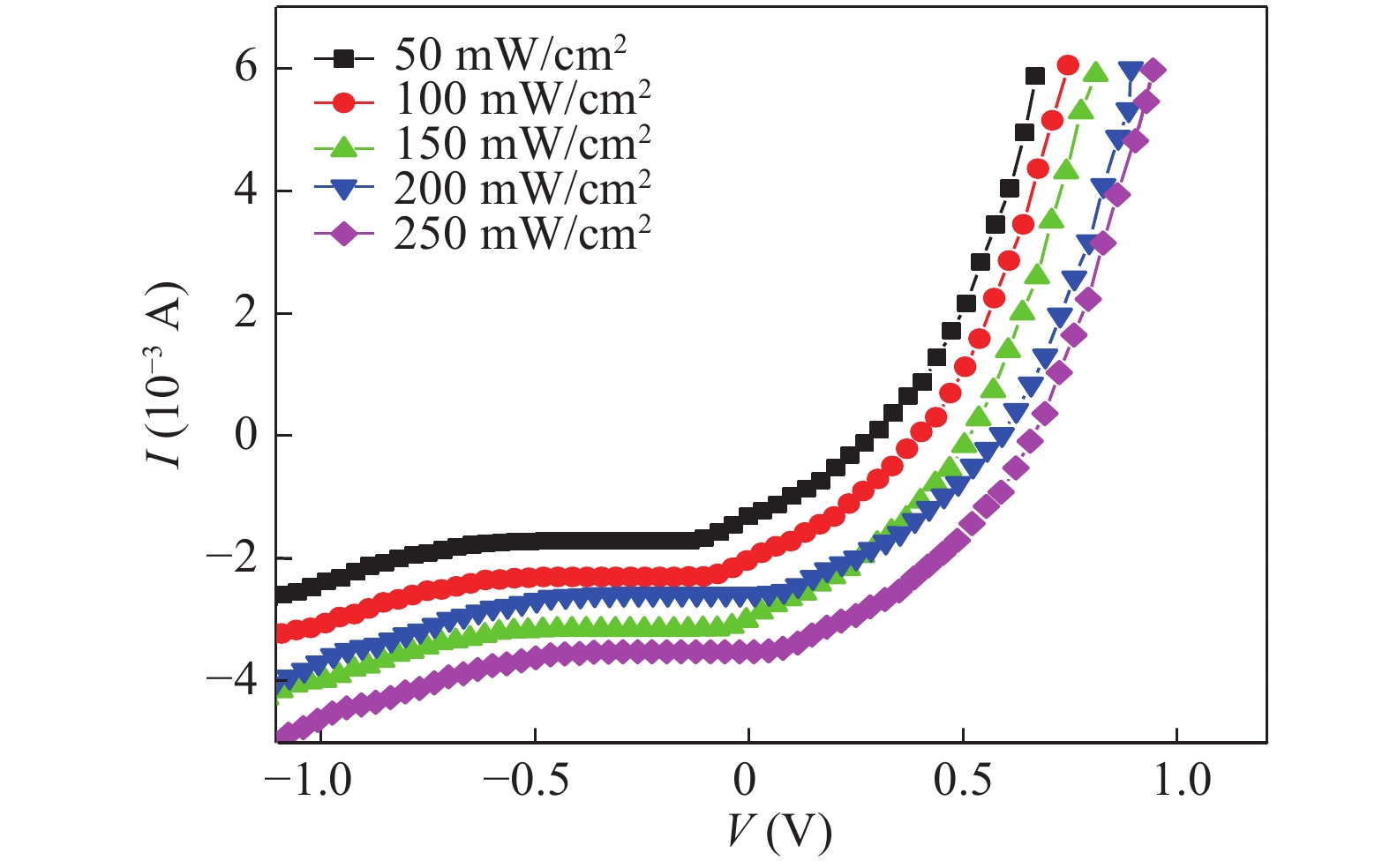
Fig. 6.  (Color online) I–V characteristics of Au/CuInGeSe4/n-Si/Al heterojunction device at different illumination powers at room temperature.

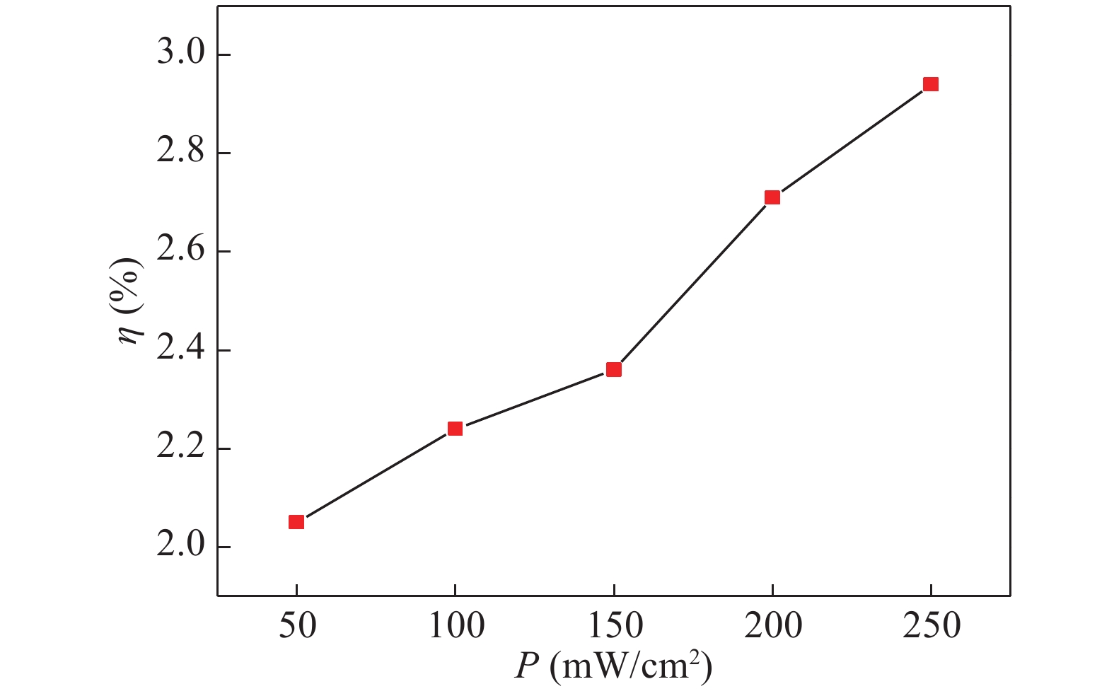
Fig. 8.  (Color online) Illumination power dependence of η for Au/CuInGeSe4/n-Si/Al heterojunction device.

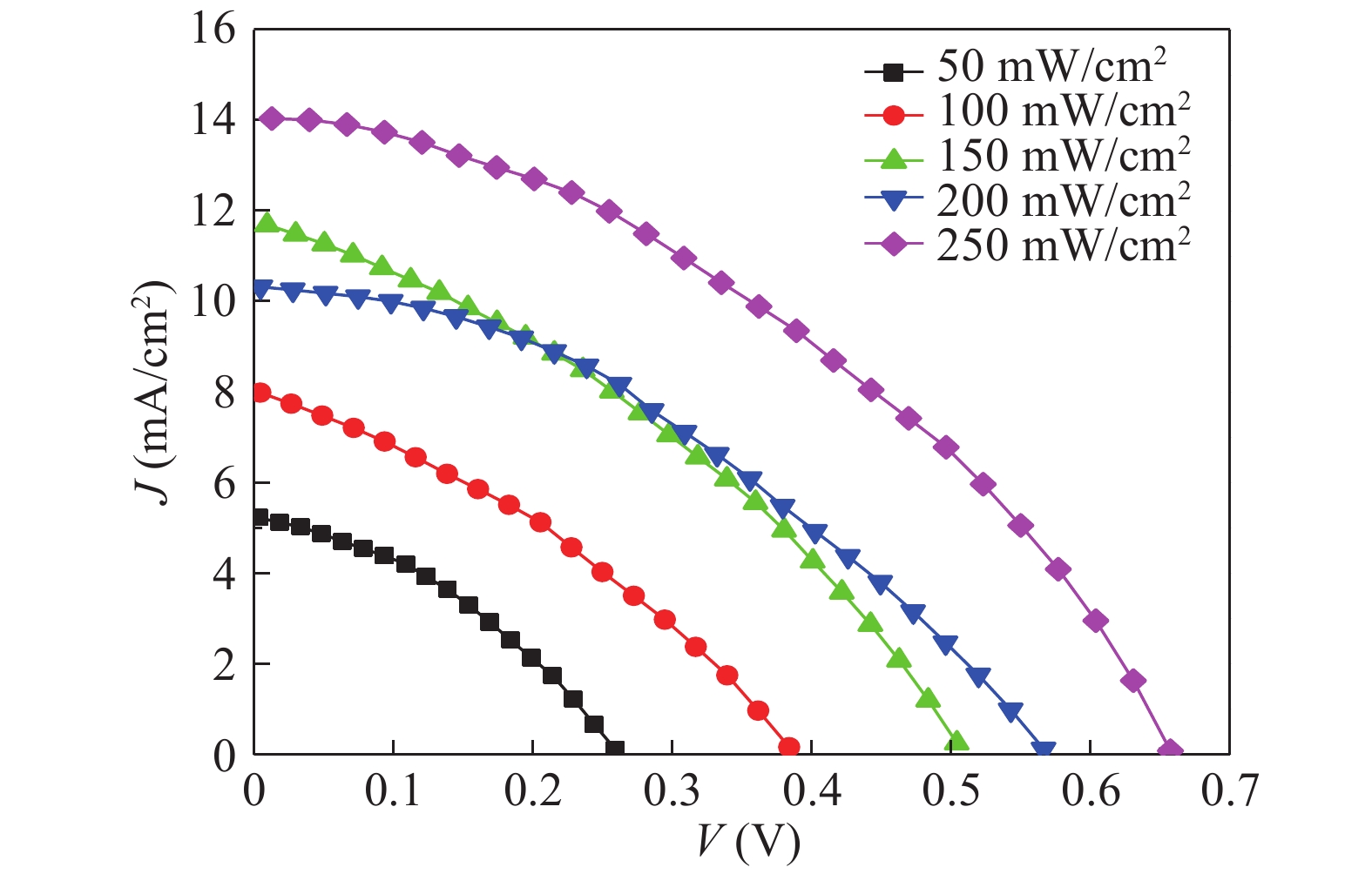
Fig. 7.  (Color online) J–V characteristics for Au/CuInGeSe4/n-Si/Al solar cell under different illumination powers.

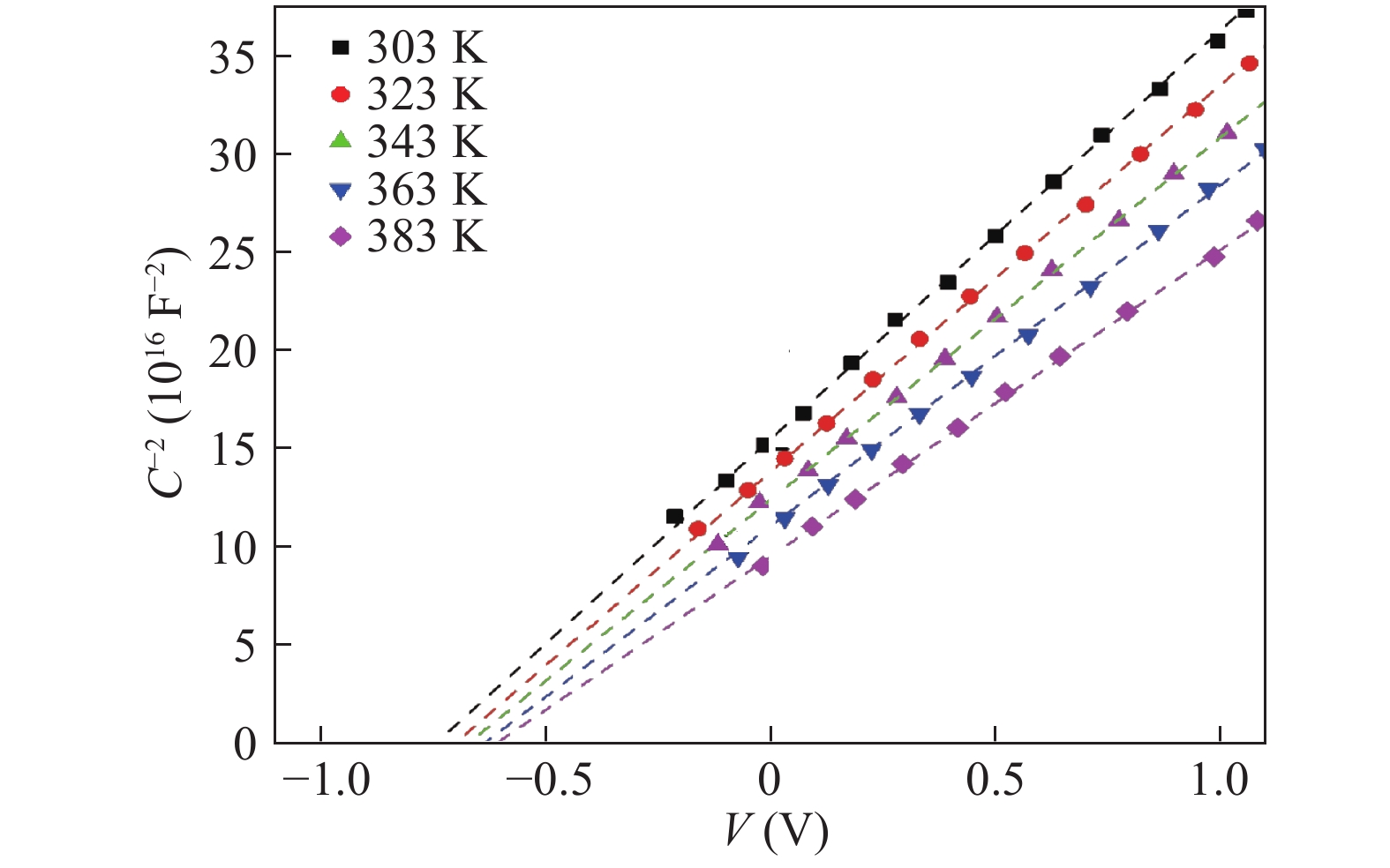
Fig. 9.  (Color online) The variation of 1/C2 versus bias voltage of the Au/CuInGeSe4/n-Si/Al heterojunction device at different temperatures.

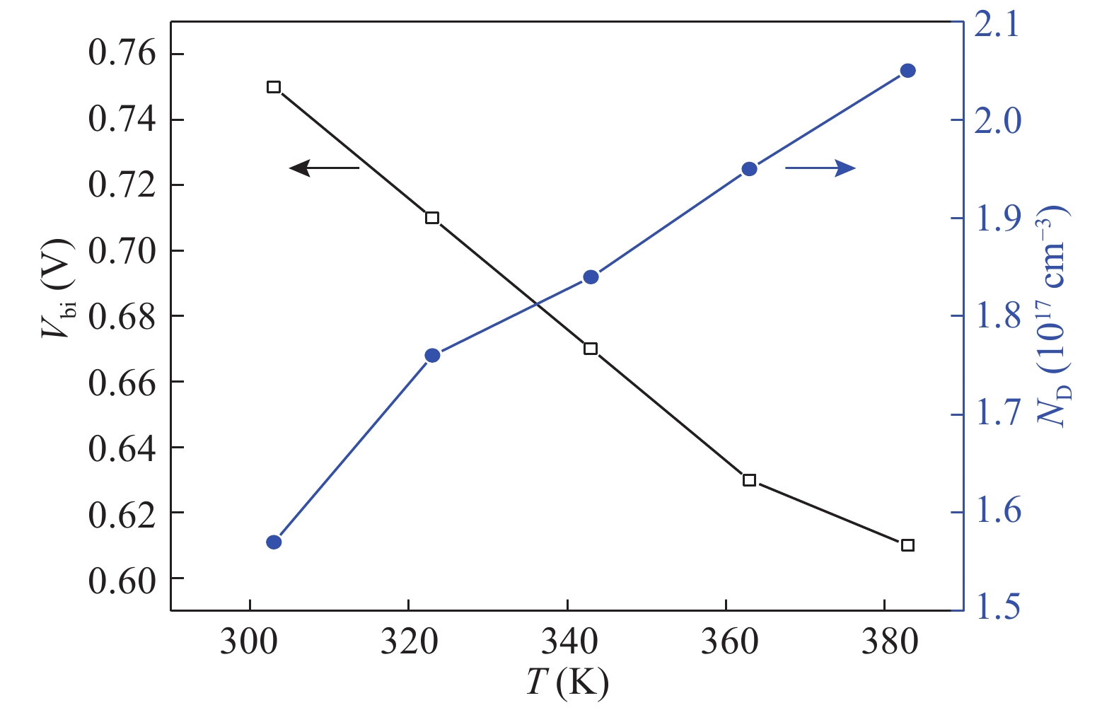
Fig. 10.  (Color online) The variation of ND and Vbi of the Au/CuInGeSe4/n-Si/Al heterojunction device at different temperatures.

Table 1.   Junction parameters determined from the dark IV characteristics of Au/CuInGeSe4/n-Si/Al heterojunction.

T (K) RR (at ±1) n RS (kΩ) Rsh (kΩ) ϕb (eV)
303 94.21 2.76 2.51 132 0.53
323 90.52 2.59 2.13 125 0.58
343 87.17 2.38 1.75 119 0.62
363 81.45 2.19 1.48 115 0.68
383 74.96 1.95 1.12 111 0.71
DownLoad: CSV

Table 2.   The solar parameters determined from the J–V curve of Au/CuInGeSe4/n-Si/Al heterojunction.

Intensity (mW/cm2) JSC VOC JM VM FF η (%)
50 5.26 0.26 3.42 0.15 0.37 2.05
100 7.98 0.38 4.97 0.21 0.39 2.24
150 10.24 0.51 6.81 0.31 0.41 2.36
200 11.75 0.62 7.22 0.32 0.38 2.71
250 14.12 0.65 9.14 0.41 0.40 2.94
DownLoad: CSV

Table 3.   Temperature dependent values of parameters determined from C–V characteristics of Au/CuInGeSe4/n-Si/Al heterojunction.

T (K) Vbi (V) ND (1017 cm−3)
303 0.75 1.57
323 0.71 1.76
343 0.67 1.84
363 0.63 1.95
383 0.61 2.05
DownLoad: CSV
[1]
Matsushita H, Katsui A. Materials design for Cu-based quaternary compounds derived from chalcopyrite-rule. J Phys Chem Solids, 2005, 66: 1933 doi: 10.1016/j.jpcs.2005.09.028
[2]
Gorgut G P, Fedorchuk A O, Kityk I V, et al. Synthesis and structural properties of CuInGeS4. J Cryst Growth, 2011, 324: 212 doi: 10.1016/j.jcrysgro.2011.02.029
[3]
Li W, Yan X, Xu W L, et al. Efficiency improvement of CIGS solar cells by a modified rear contact. Sol Energy, 2017, 157: 486 doi: 10.1016/j.solener.2017.08.054
[4]
Shah A V, Schade H, Vanecek M, et al. Thin-film silicon solar cell technology. Prog Photovoltaics Res Appl, 2004, 12: 113 doi: 10.1002/pip.533
[5]
Matsushita H, Ochiai T, Mikajiri K, et al. Preparation of CuInGeSe4 thin films by selenization method using the Cu–In–Ge evaporated layer precursors. J Phys Chem Solids, 2005, 66: 1937 doi: 10.1016/j.jpcs.2005.09.031
[6]
Matsushita H, Maeda T, Katsui A, et al. Thermal analysis and synthesis from the melts of Cu-based quaternary compounds Cu–III–IV–VI4 and Cu2–II–IV–VI4(II = Zn, Cd; III = Ga, In; IV = Ge, Sn; VI = Se). J Cryst Growth, 2000, 208: 416 doi: 10.1016/S0022-0248(99)00468-6
[7]
Hughes O H, Woolley J C, Lopez-Rivera S A, et al. Quaternary adamantine selenides and tellurides of the form I III IV VI4. Solid State Commun, 1980, 35: 573 doi: 10.1016/0038-1098(80)90585-2
[8]
Contreras M A, Ramanathan K, Abushama J, et al. Diode characteristics in state-of-the-art ZnO/CdS/ Cu(In1-xGax)Se2 solar cells. Prog Photovolt Res Appl, 2005, 13: 209 doi: 10.1002/pip.626
[9]
Abd El-Rahman K F, Darwish A A A, El-Shazly E A A. Electrical and photovoltaic properties of SnSe/Si heterojunction. Mater Sci Semicond Process, 2014, 25: 123 doi: 10.1016/j.mssp.2013.10.003
[10]
Lin Y, Chen X. Advanced nano deposition methods. Weinheim: Wiley-VCH Verlag GmbH & Co. KGaA, 2016
[11]
Cuomo J J, Rossnagel S M, Haufman H R, et al. Handbook of ion beam processing technology: principles, deposition, film modification, and synthesis. Westwood: Noyes Publications, 1989
[12]
Cividjian N, Hagen C W. Electron-beam-induced nanometer-scale deposition. Adv Imaging Electron Phys, 2006, 143: 1 doi: 10.1016/S1076-5670(06)43001-9
[13]
Strehl P. Beam Instrumentation and Diagnostics. Berlin: Springer, 2006
[14]
El Radaf I M, Nasr M, Mansour A M. Structural, electrical and photovoltaic properties of CoS/Si heterojunction prepared by spray pyrolysis. Mater Res Express, 2018, 5: 015904 doi: 10.1088/2053-1591/aaa25e
[15]
Hassan N, Mansour A M, Roushdy N, et al. Optical sensing performance characteristics of Schottky devices diodes based nano-particle disodium 6-hydroxy-5-[(2-methoxy-5-methyl-4-sulfophenyl)azo]-2-naphthalenesulfonate thin films: A comparison study. Optik (Stuttg), 2018, 158: 1255 doi: 10.1016/j.ijleo.2017.12.203
[16]
Nasr M, El Radaf I M, Mansour A M. Current transport and capacitance–voltage characteristics of an n-PbTe/p-GaP heterojunction prepared using the electron beam deposition technique. J Phys Chem Solids, 2018, 115: 283 doi: 10.1016/j.jpcs.2017.12.029
[17]
Farag A A M, Terra F S, Mahmoud G M, et al. Study of Gaussian distribution of inhomogeneous barrier height for n-InSb/p-GaAs heterojunction prepared by flash evaporation. J Alloys Compd, 2009, 481: 427 doi: 10.1016/j.jallcom.2009.03.004
[18]
Farag A A M, Soliman H S, Atta A A. Analysis of dark and photovoltaic characteristics of Au/Pyronine G(Y)/p-Si/Al heterojunction. Synth Met, 2012, 161: 2759 doi: 10.1016/j.synthmet.2011.10.017
[19]
Farag A A M, Terra F S, Fahim G M M, et al. Current transport and capacitance-voltage characteristics of n-InSb/p-GaP prepared by flash evaporation and liquid phase epitaxy. Met Mater Int, 2012, 18: 509 doi: 10.1007/s12540-012-3020-4
[20]
Gupta R K, Aydın M E, Yakuphanoglu F. Photoconducting and electrical properties of Al/TIPS-pentacene/p-Si/Al hybrid diode for optical sensor applications. Synth Met, 2011, 161: 2355 doi: 10.1016/j.synthmet.2011.09.002
[21]
Yahia I S, Farag A A M, Yakuphanoglu F, et al. Temperature dependence of electronic parameters of organic Schottky diode based on fluorescein sodium salt. Synth Met, 2011, 161: 881 doi: 10.1016/j.synthmet.2011.02.016
[22]
Yahia I S, Fadel M, Sakr G B, et al. Analysis of current–voltage characteristics of Al/p-ZnGa2Se4/n-Si nanocrystalline heterojunction diode. J Alloys Compd, 2011, 509: 4414 doi: 10.1016/j.jallcom.2011.01.068
[23]
Soliman H S, Farag A A M, Khosifan N M, et al. Electronic and photovoltaic properties of Au/pyronine G(Y)/p-GaAs/Au:Zn heterojunction. J Alloys Compd, 2012, 530: 157 doi: 10.1016/j.jallcom.2012.03.053
[24]
Çetinkaya H G, Tecimer H, Uslu H, et al. Photovoltaic characteristics of Au/PVA (Bi-doped)/n-Si Schottky barrier diodes (SBDs) at various temperatures. Curr Appl Phys, 2013, 13: 1150 doi: 10.1016/j.cap.2013.03.010
[25]
Farag A A M, Terra F S, Ashery A, et al. Structural and electrical characteristics of n-InSb/p-GaAs heterojunction prepared by liquid phase epitaxy. J Alloys Compd, 2014, 615: 604 doi: 10.1016/j.jallcom.2014.06.058
[26]
Farag A A M, Terra F S, Ashery A, et al. Structural and electrical characterization of n-InAs/p-GaP heterojunctions prepared by vacuum flash evaporation and liquid phase epitaxy. Optoelectron. Adv Mater – RAPID Commun, 2017, 11: 82
[27]
Ahmad Z, Sayyad M H, Yaseen M, et al. Investigation of 5,10,15,20-Tetrakis(3-,5--Di-Tert-Butylphenyl)Porphyrinatocopper(II) for Electronics Applications. Int J Chem Mol Nucl Mater Metall Eng, 2011, 5: 380
[28]
Farag A A M, Terra F S, Ashery A, et al. Temperature dependence of J-V and C-V characteristics of n-InAs/p-GaAs heterojunctions prepared by flash evaporation technique and liquid phase epitaxy. Indian Pure Appl Phys, 2018, 56: 203
[29]
El-Nahass M M, Metwally H S, El-Sayed H E A , et al. Electrical and photovoltaic properties of FeTPPCl/p-Si heterojunction. Synth Met, 2011, 161: 2253 doi: 10.1016/j.synthmet.2011.08.030
[30]
Hameed T A, El Radaf I M, Elsayed-Ali H E. Characterization of CuInGeSe4 thin films and Al/n-Si/p-CuInGeSe4/Au heterojunction device. J Mater Sci Mater Electron, 2018, 29: 12584 doi: 10.1007/s10854-018-9375-7
[31]
Sze S M, Ng K K. Physics of semiconductor devices. New York: Wiley-Interscience, 2007
  • Search

    Advanced Search >>

    GET CITATION

    shu

    Export: BibTex EndNote

    Article Metrics

    Article views: 3601 Times PDF downloads: 46 Times Cited by: 0 Times

    History

    Received: 11 May 2018 Revised: 17 June 2018 Online: Uncorrected proof: 13 September 2018Published: 13 December 2018

    Catalog

      Email This Article

      User name:
      Email:*请输入正确邮箱
      Code:*验证码错误
      I. M. El Radaf, A. M. Mansour, G. B. Sakr. Fabrication, electrical and photovoltaic characteristics of CuInGeSe4/n-Si diode[J]. Journal of Semiconductors, 2018, 39(12): 124010. doi: 10.1088/1674-4926/39/12/124010 I M El Radaf, A M Mansour, G B Sakr, Fabrication, electrical and photovoltaic characteristics of CuInGeSe4/n-Si diode[J]. J. Semicond., 2018, 39(12): 124010. doi: 10.1088/1674-4926/39/12/124010.Export: BibTex EndNote
      Citation:
      I. M. El Radaf, A. M. Mansour, G. B. Sakr. Fabrication, electrical and photovoltaic characteristics of CuInGeSe4/n-Si diode[J]. Journal of Semiconductors, 2018, 39(12): 124010. doi: 10.1088/1674-4926/39/12/124010

      I M El Radaf, A M Mansour, G B Sakr, Fabrication, electrical and photovoltaic characteristics of CuInGeSe4/n-Si diode[J]. J. Semicond., 2018, 39(12): 124010. doi: 10.1088/1674-4926/39/12/124010.
      Export: BibTex EndNote

      Fabrication, electrical and photovoltaic characteristics of CuInGeSe4/n-Si diode

      doi: 10.1088/1674-4926/39/12/124010
      More Information
      • Corresponding author: email: amamansour@gmail.com
      • Received Date: 2018-05-11
      • Revised Date: 2018-06-17
      • Published Date: 2018-12-01

      Catalog

        /

        DownLoad:  Full-Size Img  PowerPoint
        Return
        Return