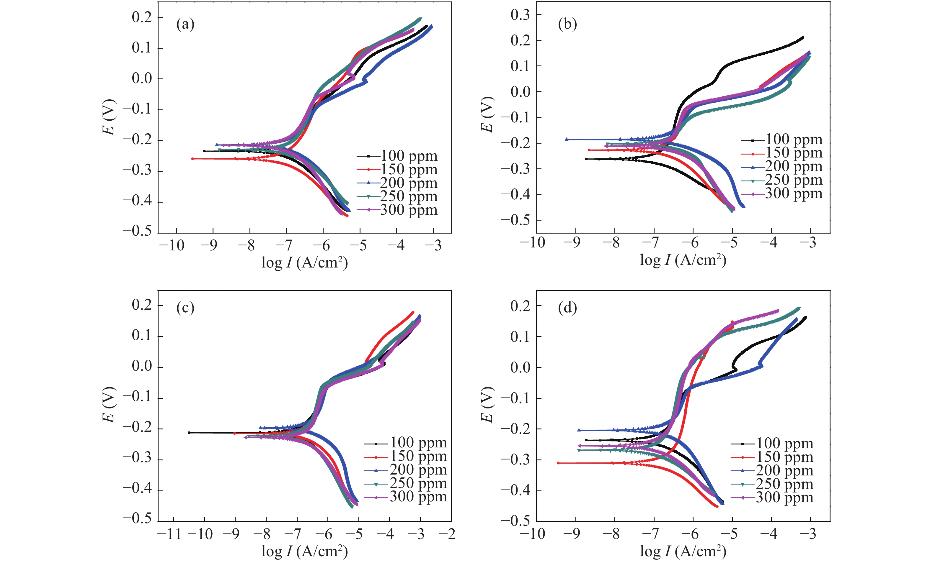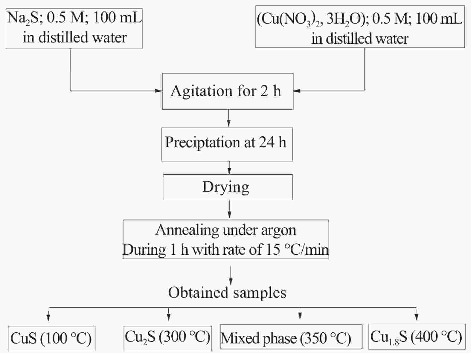
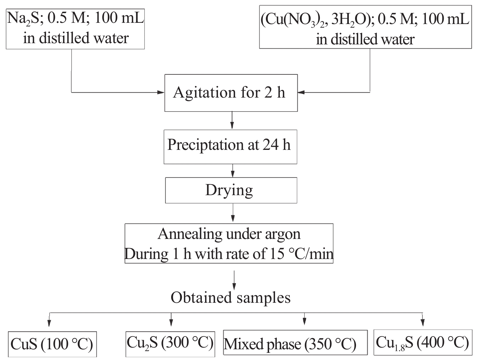
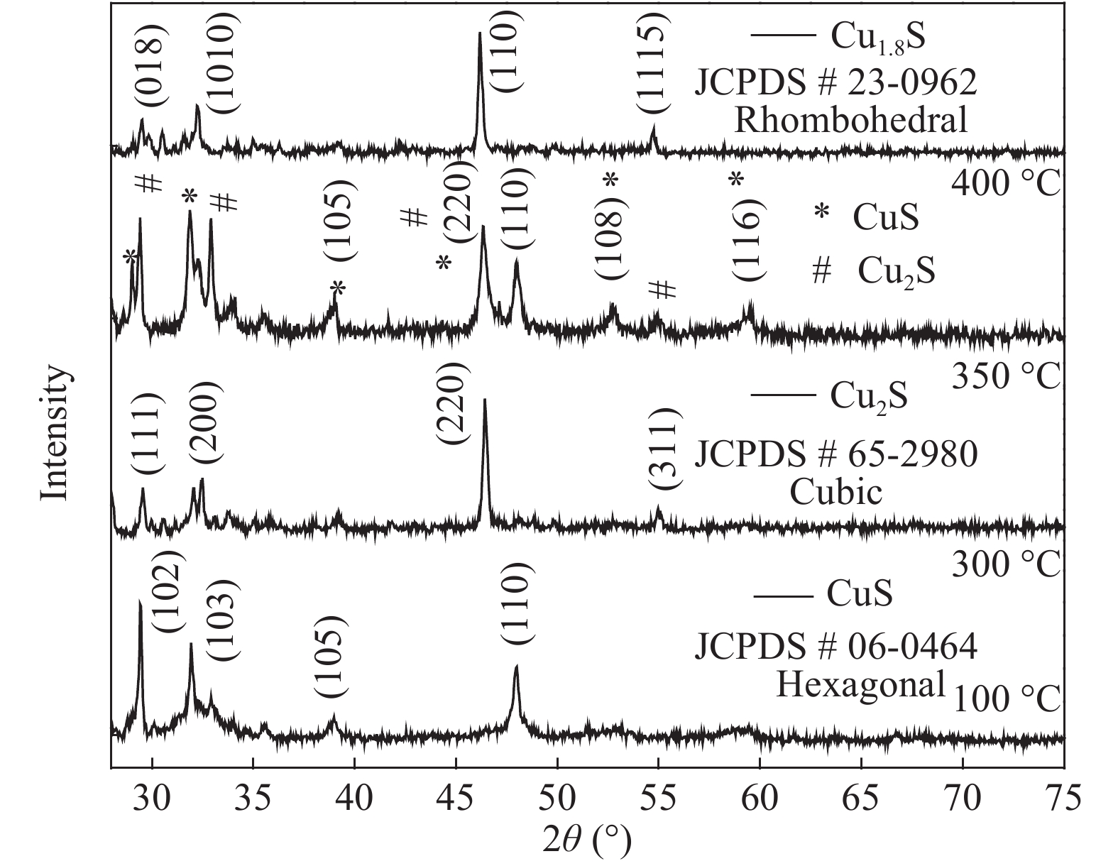
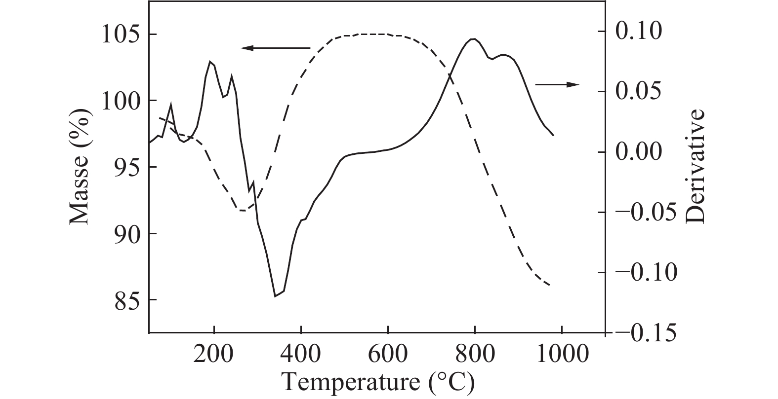
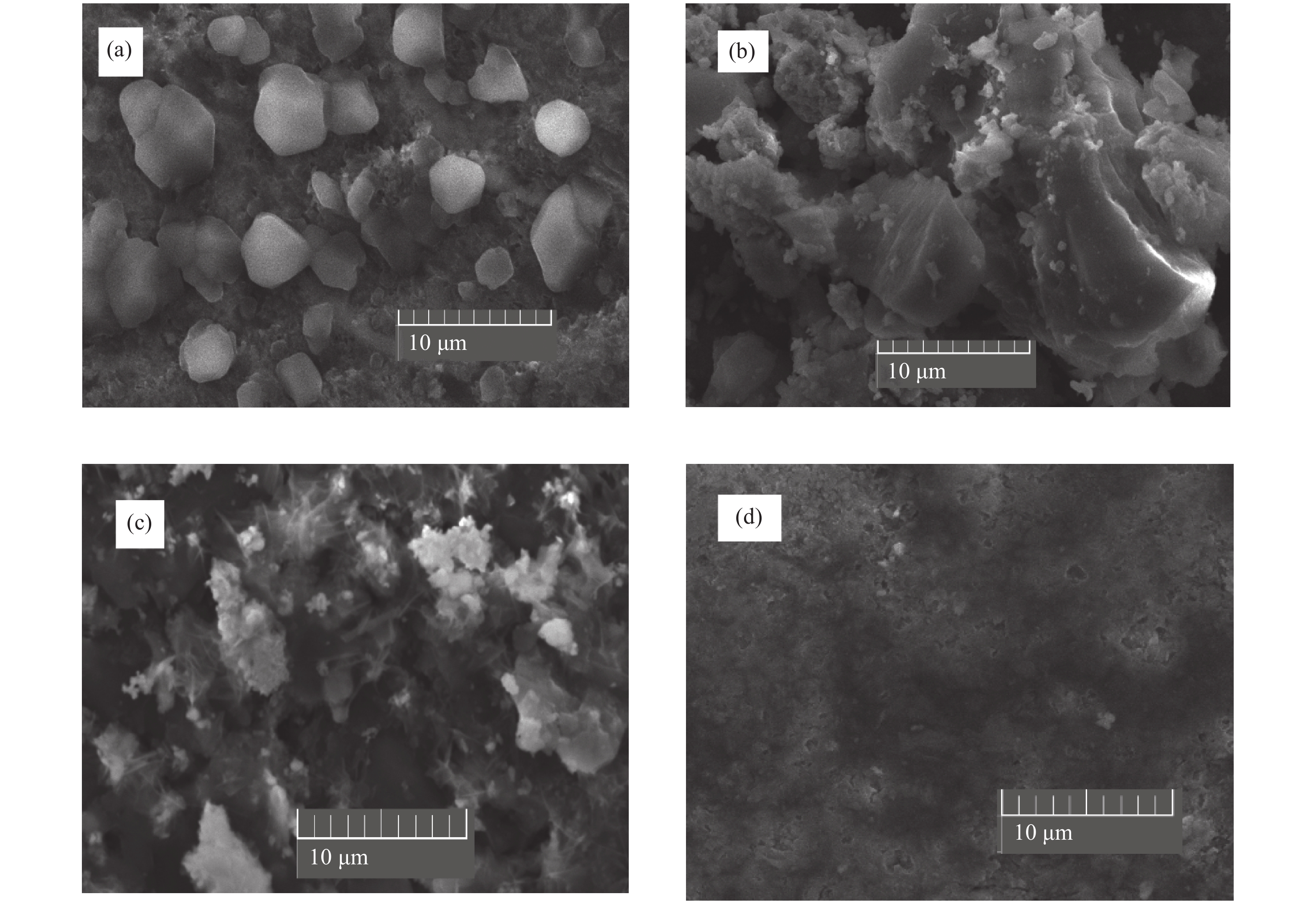
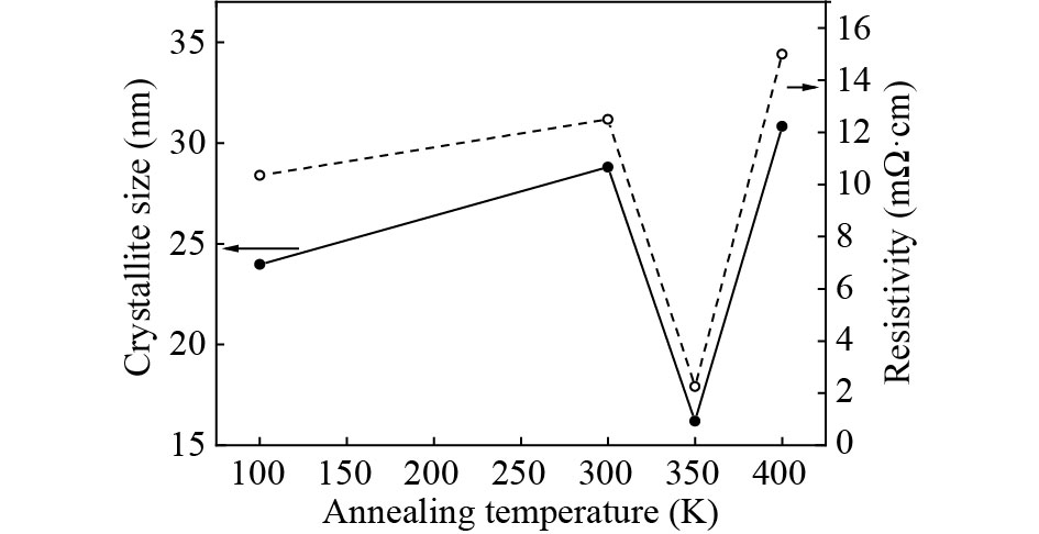
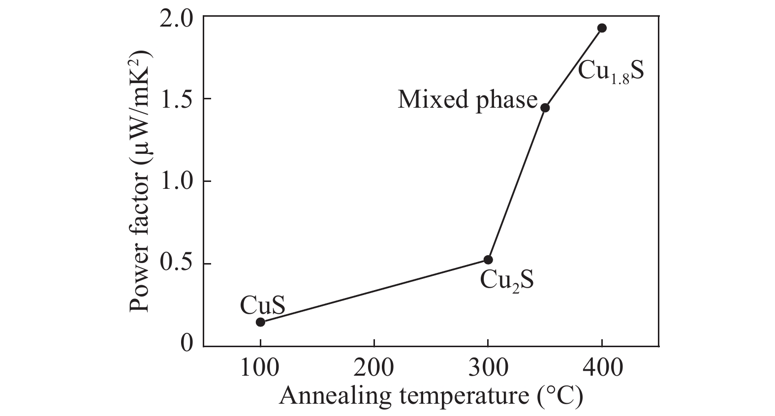
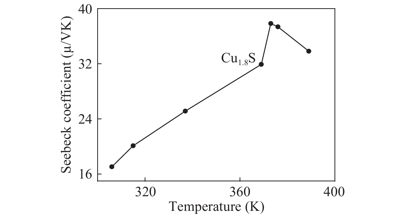
Over the past few years, Cu-based materials have been intensively studied focusing on their structural and thermoelectric properties. In this work, copper sulphide powders were synthesized by the sol-gel method. The chemical composition and the morphological properties of the obtained samples were analyzed by X-ray diffraction, differential thermal analysis, and scanning electron microscopy. It is shown that the decomposition from one phase to another can be obtained by annealing. The electrical resistivity and the crystallite size were found to be strongly affected by the phase transition. Thermoelectric analyses showed that the digenite phase exhibits the highest power factor at room temperature. The Seebeck coefficient of the compound Cu1.8S shows a pronounced peak at the γ–β transition temperature. This behavior was statistically explained in terms of a dramatic increase in the disorder in the atoms-carriers ensemble.
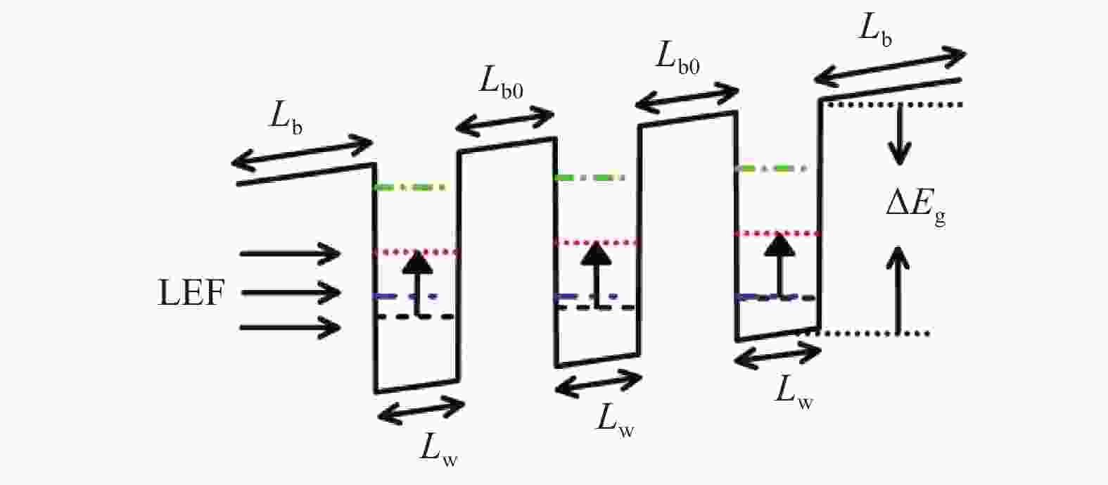
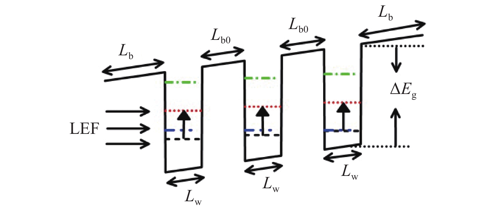
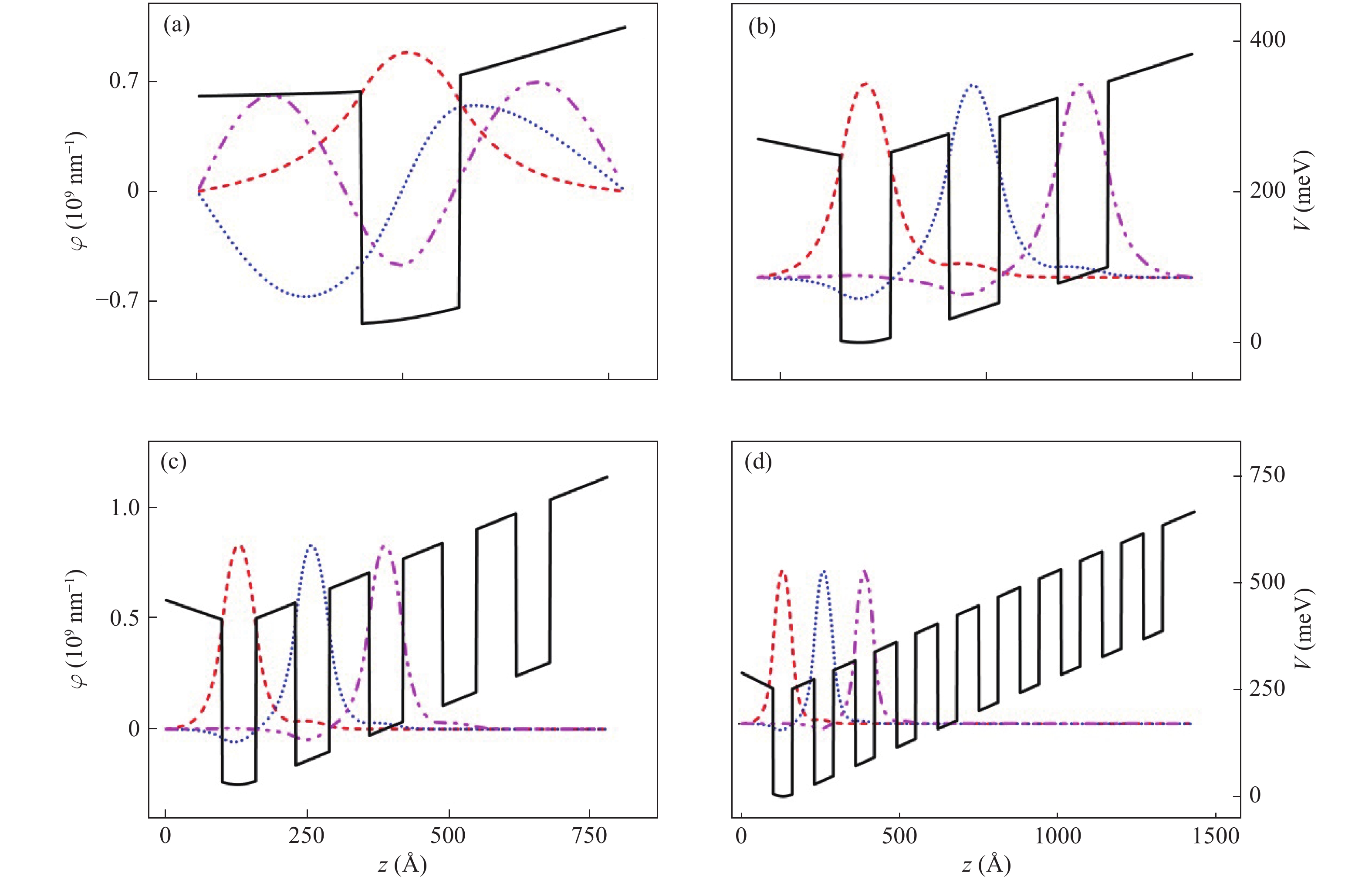
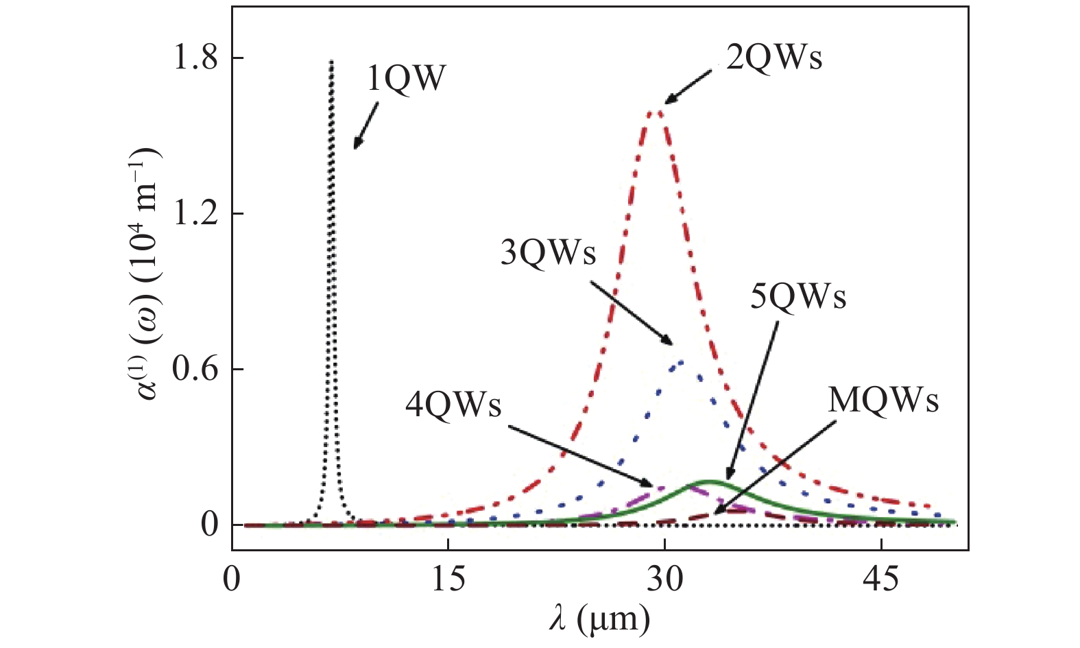
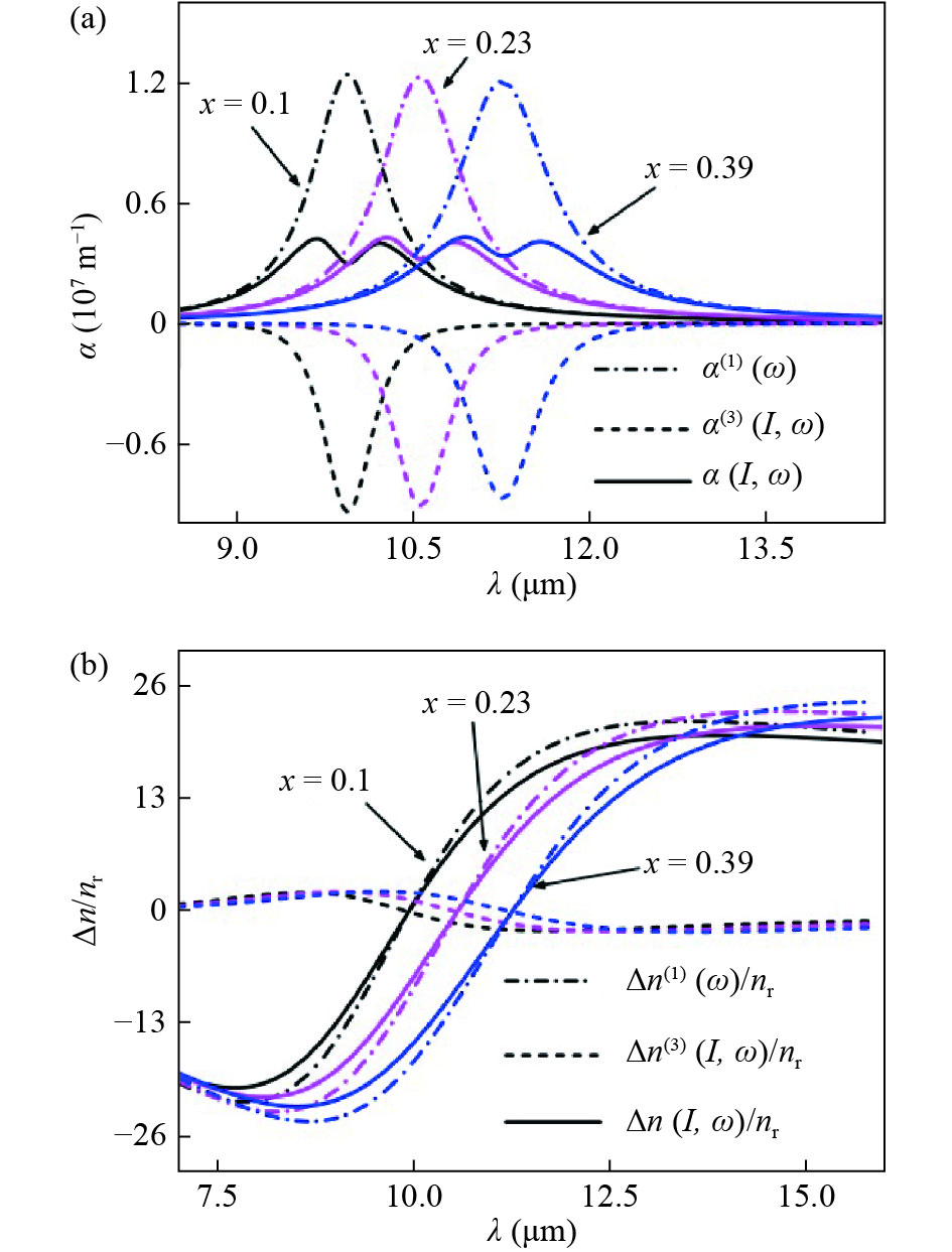
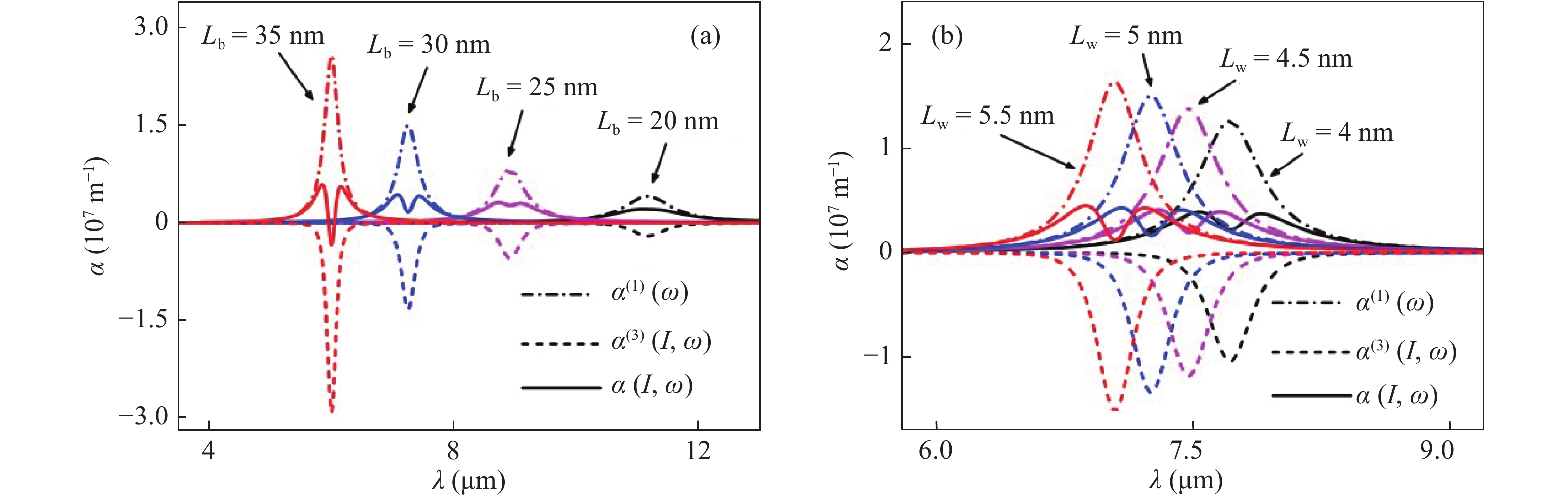
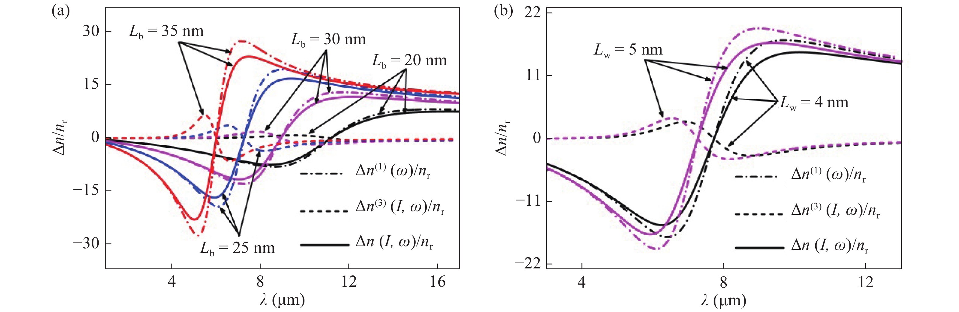
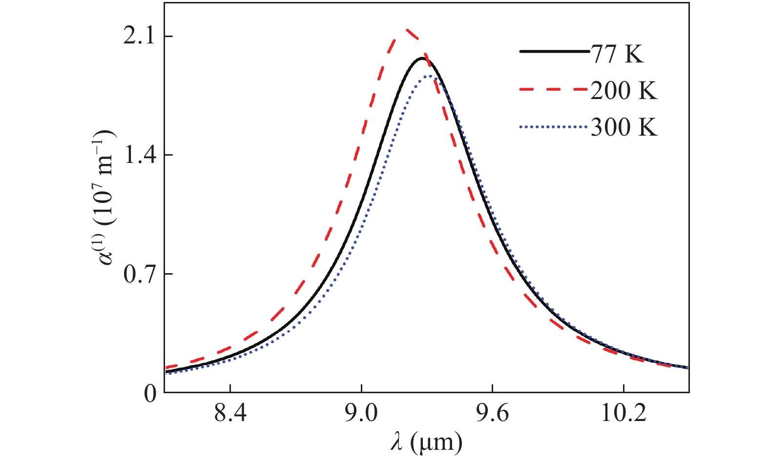
Based on the effective mass approximation, the Schrödinger equation and Poisson equation in GaAs/ AlxGa1−xAs multi-quantum wells (MQWs) are self-consistently solved to obtain the wave functions and energy levels of electrons in the conduction band for the ground first excited state by considering a lateral electric field (LEF). Then, the effects of size, ternary mixed crystal, doping concentration, and temperature on linear and nonlinear intersubband optical absorption coefficients (IOACs), and refractive index changes (RICs) due to the transition between ground states and the first excited states of electrons are discussed based on Fermi’s golden rule. The results show that, under a fixed LEF, with increase of Al composition and doping concentration, the IOACs produce a red shift. With increases of both widths of the wells and barriers IOACs appear as blue shifts and their amplitudes increase, but the barrier width change is much more important to affect nonlinear IOACs, whereas increasing the temperature results in a blue shift first and then a red shift of IOACs. When the other parameters are fixed but there is an increase in the LEF, IOACs occur with a blue shift, and the RICs have similar properties.


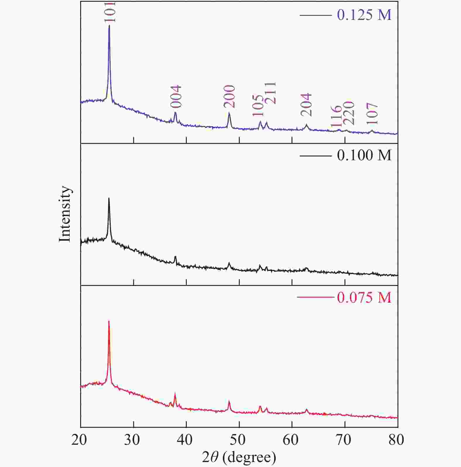
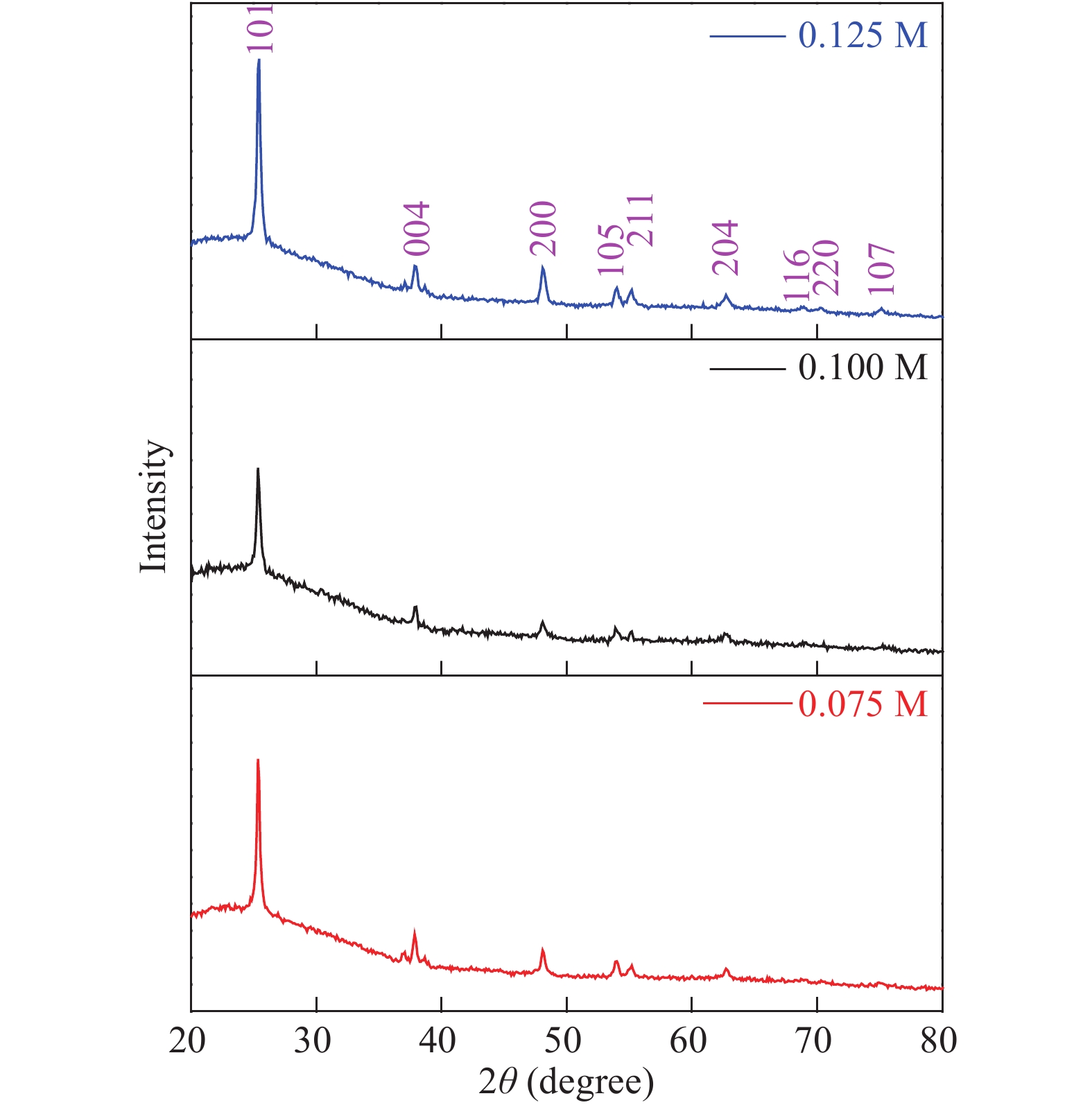
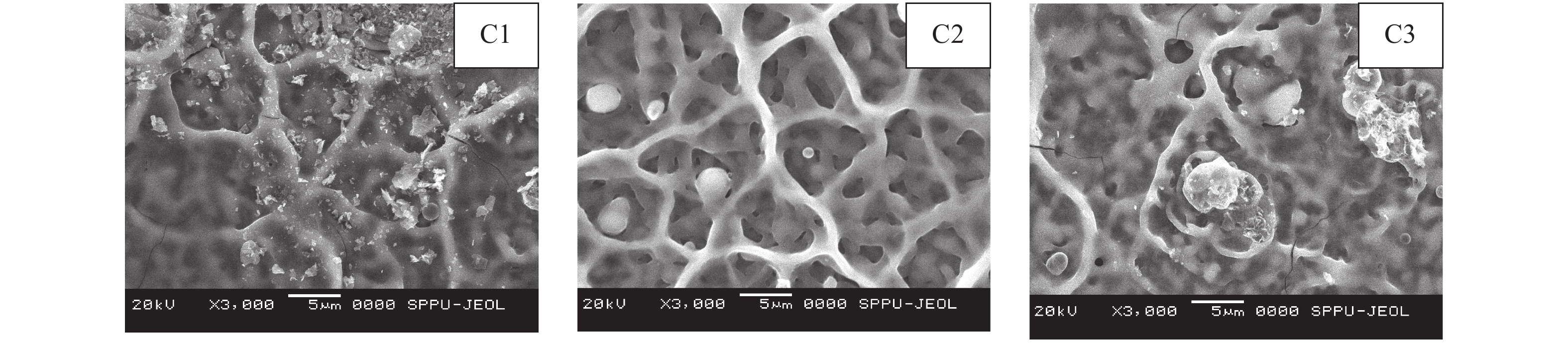
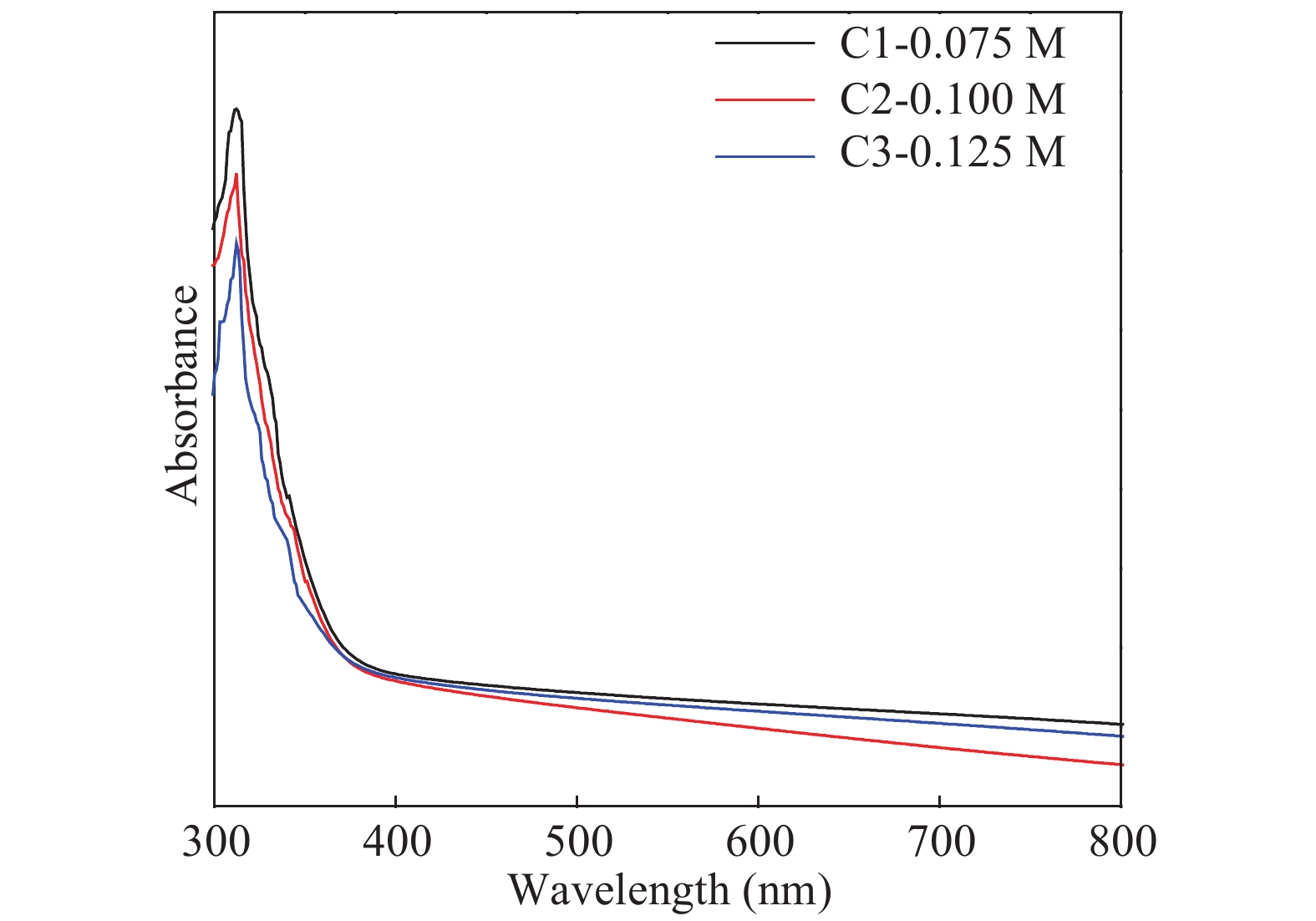
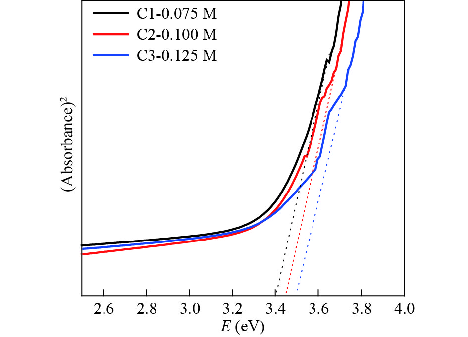
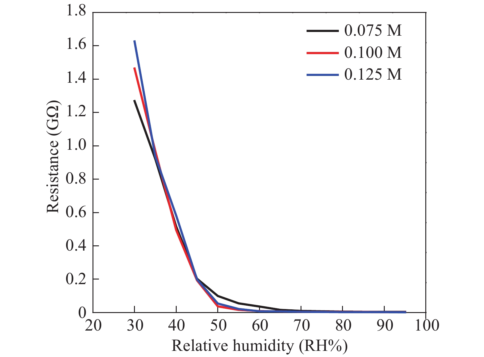
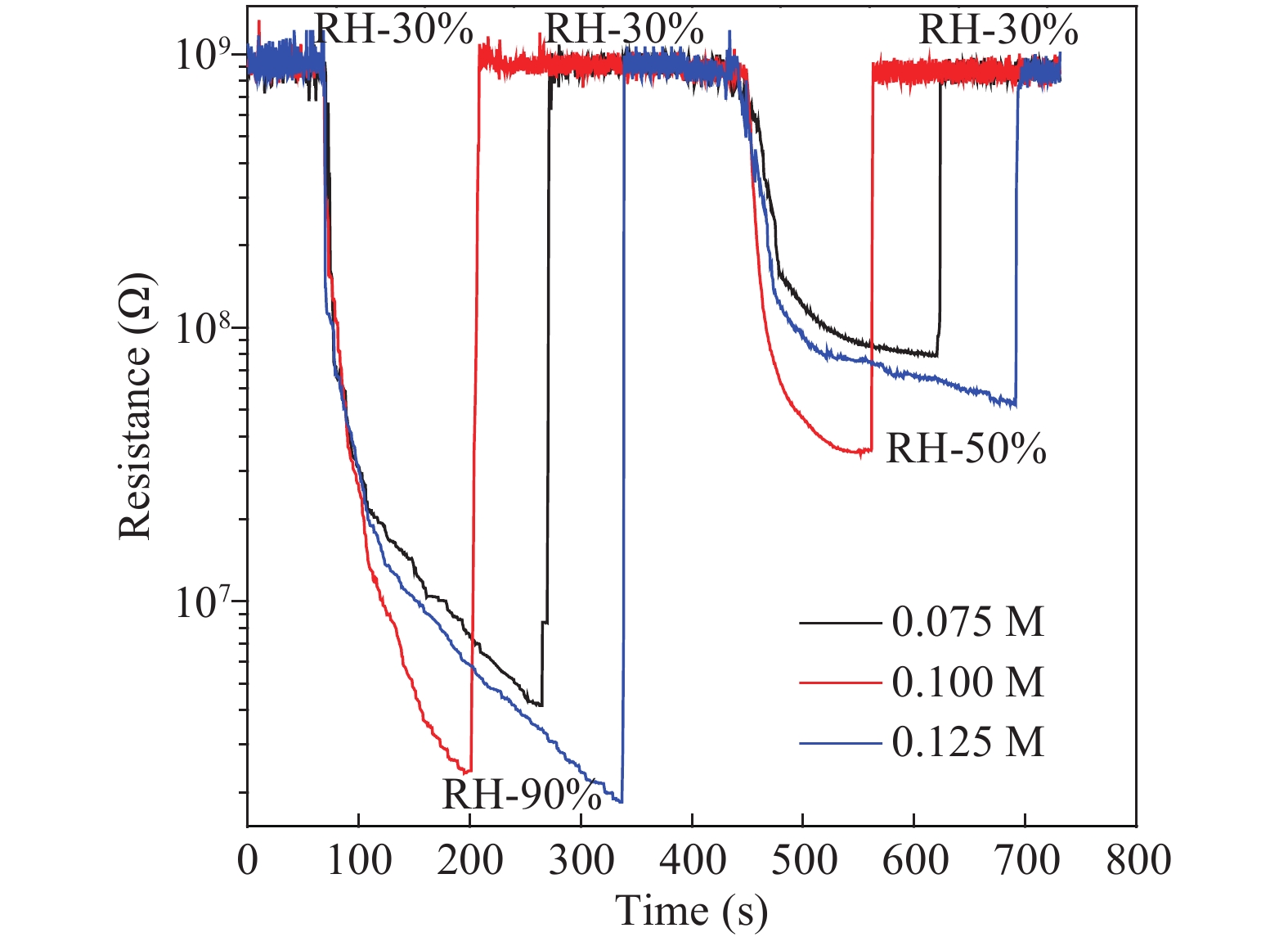
In the present paper, the influence of precursor concentration on the structural, optical, and humidity sensing properties of spray-deposited titanium dioxide (TiO2) films are investigated. The TiO2 thin films were successfully deposited by spraying different precursor concentrations such as 0.075 M, 0.1 M, and 0.125 M of titanium trichloride solution onto glass substrates. X-ray diffractometry (XRD) studies confirmed the polycrystalline anatase phase of TiO2 with dominant (101) plane. The crystallite size was found to increase with the increase in precursor concentration. The micro-strain and dislocation density in the film was observed to decrease as the crystallite size increased. The UV–vis spectra confirmed the optical absorbance edge of the samples shifted toward lower wavelengths with increased precursor concentration. The humidity sensing properties of the synthesized material were measured by monitoring the change in resistance of the sample with the change in relative humidity. The material synthesized with 0.1 M precursor concentration, by using the spray pyrolysis method, shows good sensitivity and has a response time of 77.5 s and fast recovery time of 3 s.


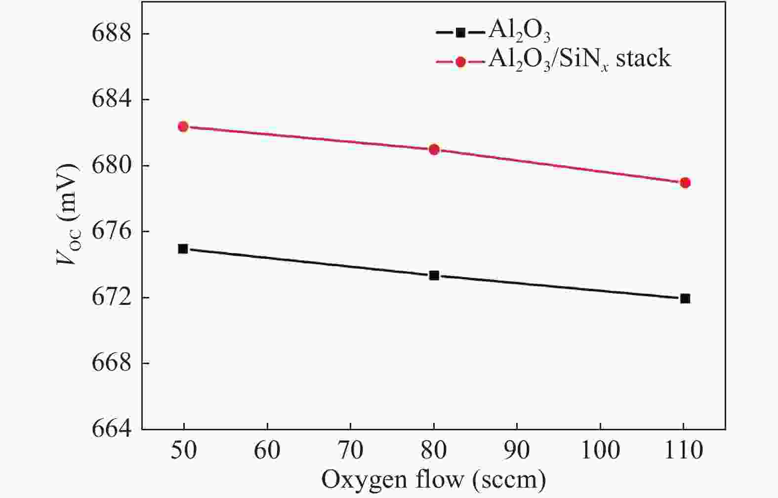
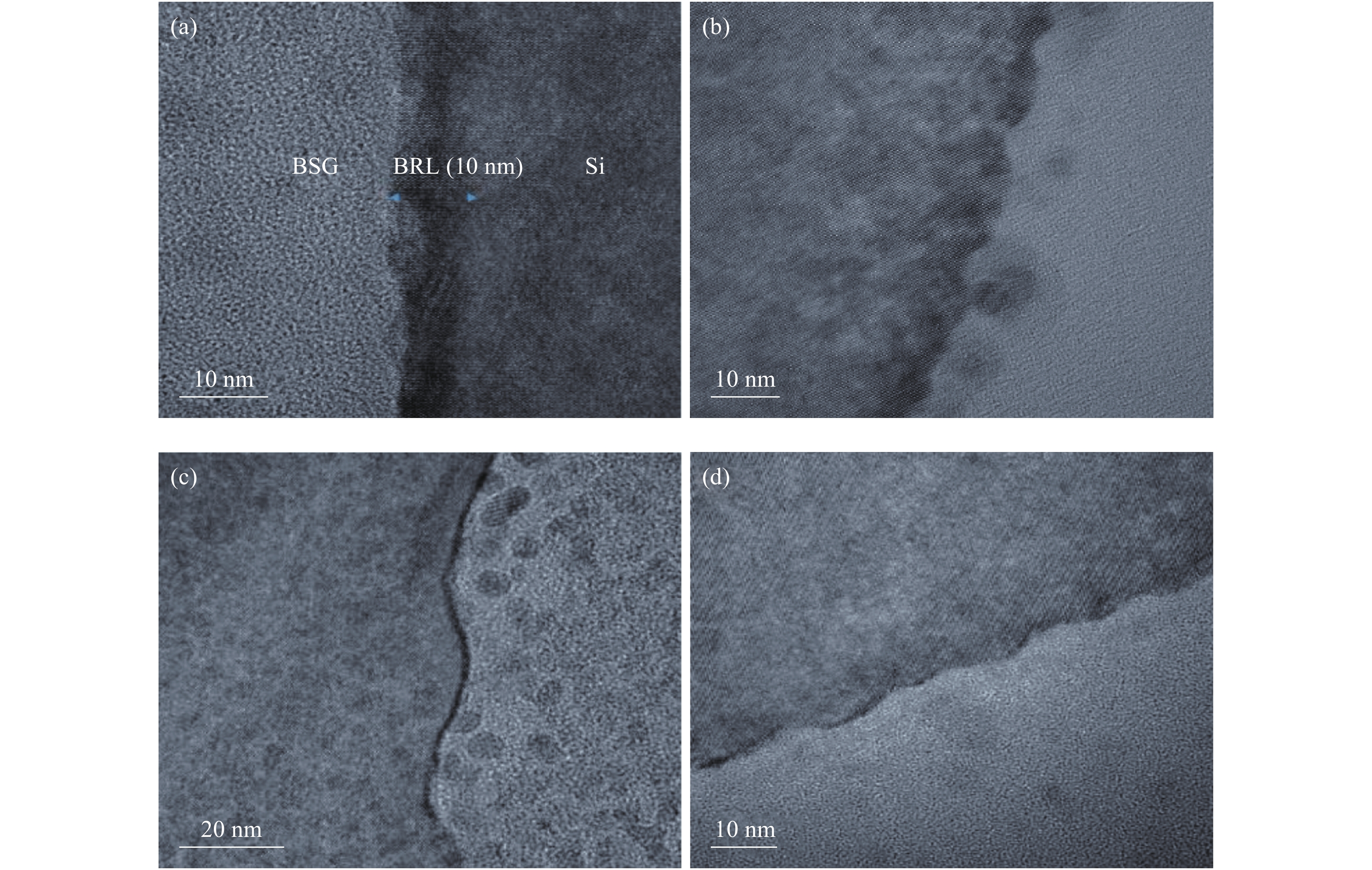
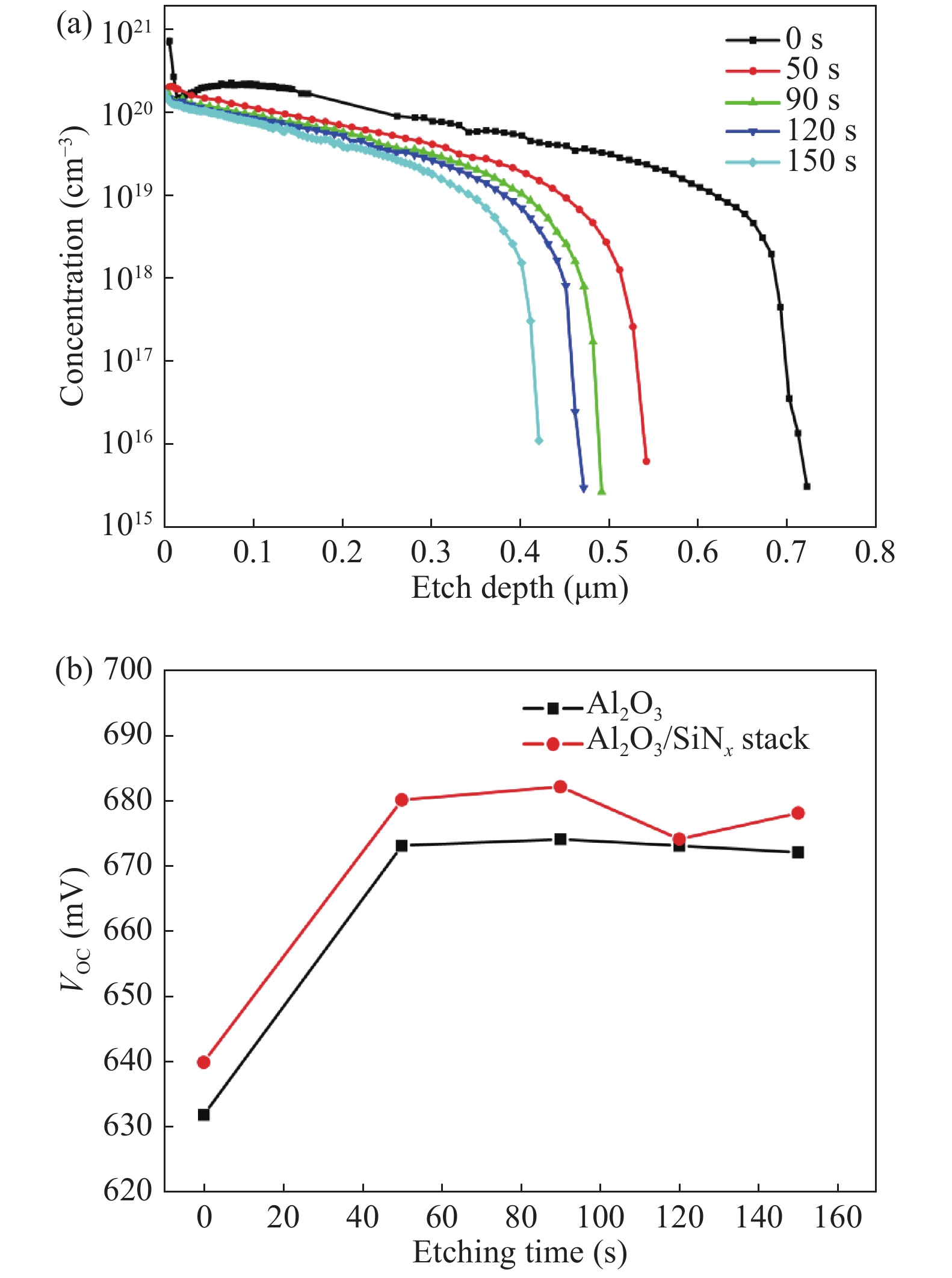
In boron-doped p+–n crystalline silicon (Si) solar cells, p-type boron doping control and surface passivation play a vital role in the realization of high-efficiency and low cost pursuit. In this study, boron-doped p+-emitters are formed by boron diffusion in an open-tube furnace using borontribromide (BBr3) as precursor. The formed emitters are characterized in detail in terms of shape of the doping profile, surface doping concentration, junction depth, sheet resistance and removal of the boron-rich layer (BRL). In the aspect of BRL removal, three different methods were adopted to investigate their influence on device performance. The results demonstrate that our proposed chemical etch treatment (CET) with the proper etching time could be an effective way to remove the BRL. After removal of the BRL, Al2O3/SiNx stacks are deposited by atomic layer deposition (ALD) and plasma-enhanced chemical vapor deposition (PECVD) to passivate the cell surface. It was found that a reasonably-high implied Voc of 680 mV has been achieved for the fabricated n-type Si solar cells.

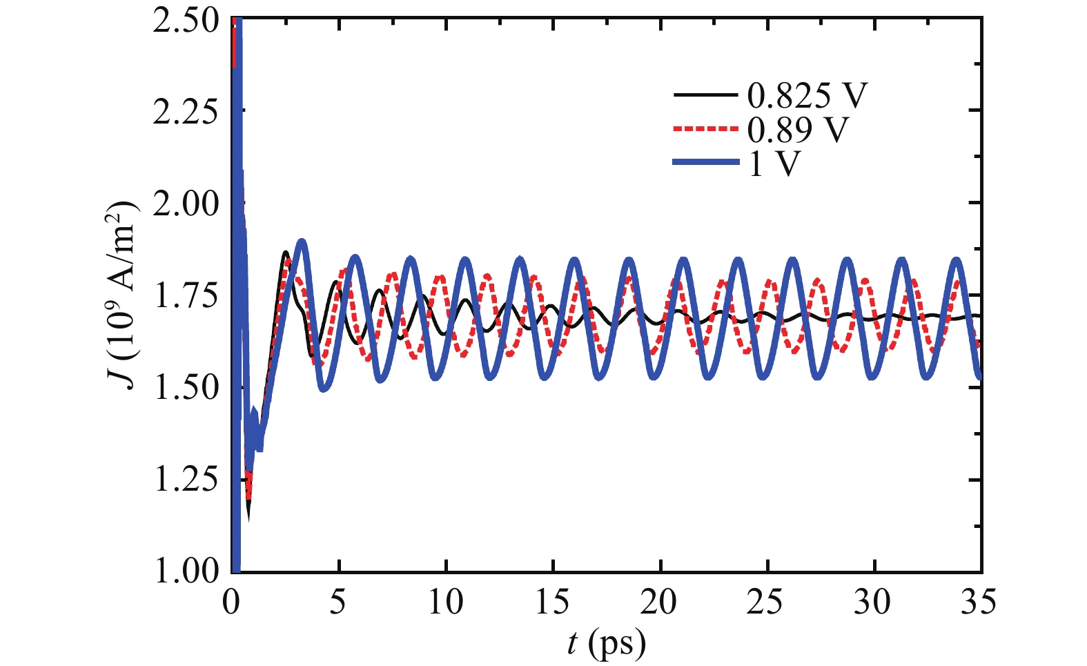
We have theoretically studied current self-oscillations in double-layer graphene n+nn+ diodes driven by dc bias with the help of a time-dependent hydrodynamic model. The current self-oscillation results from resonant tunneling in the double-layer graphene structure. A detailed investigation of the dependence of the current self-oscillations on the applied bias has been carried out. The frequencies of current self-oscillations are in the terahertz (THz) region. The double-layer graphene n+nn+ device studied here may be presented as a THz source at room temperature.

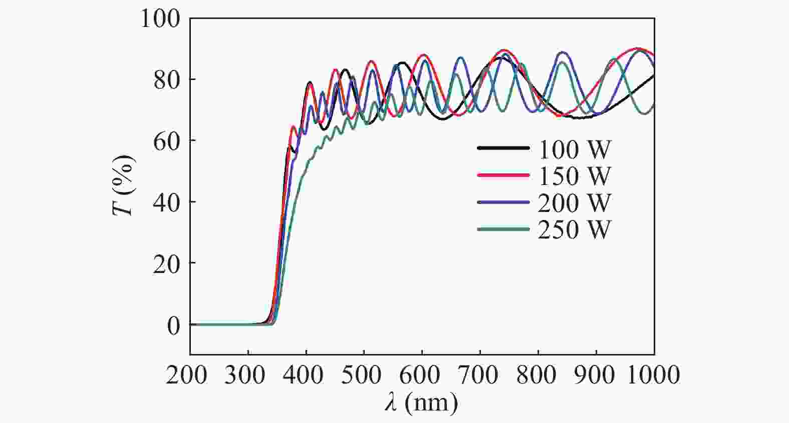
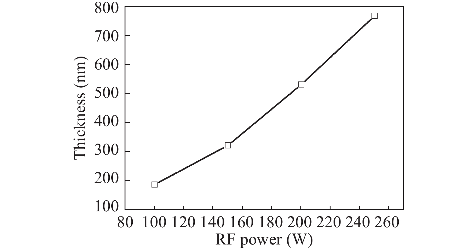
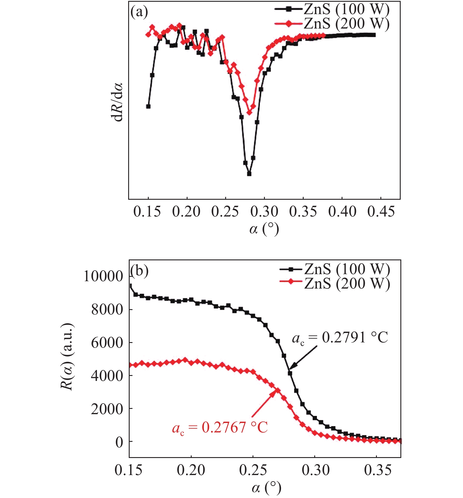
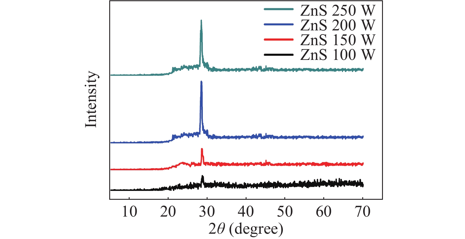
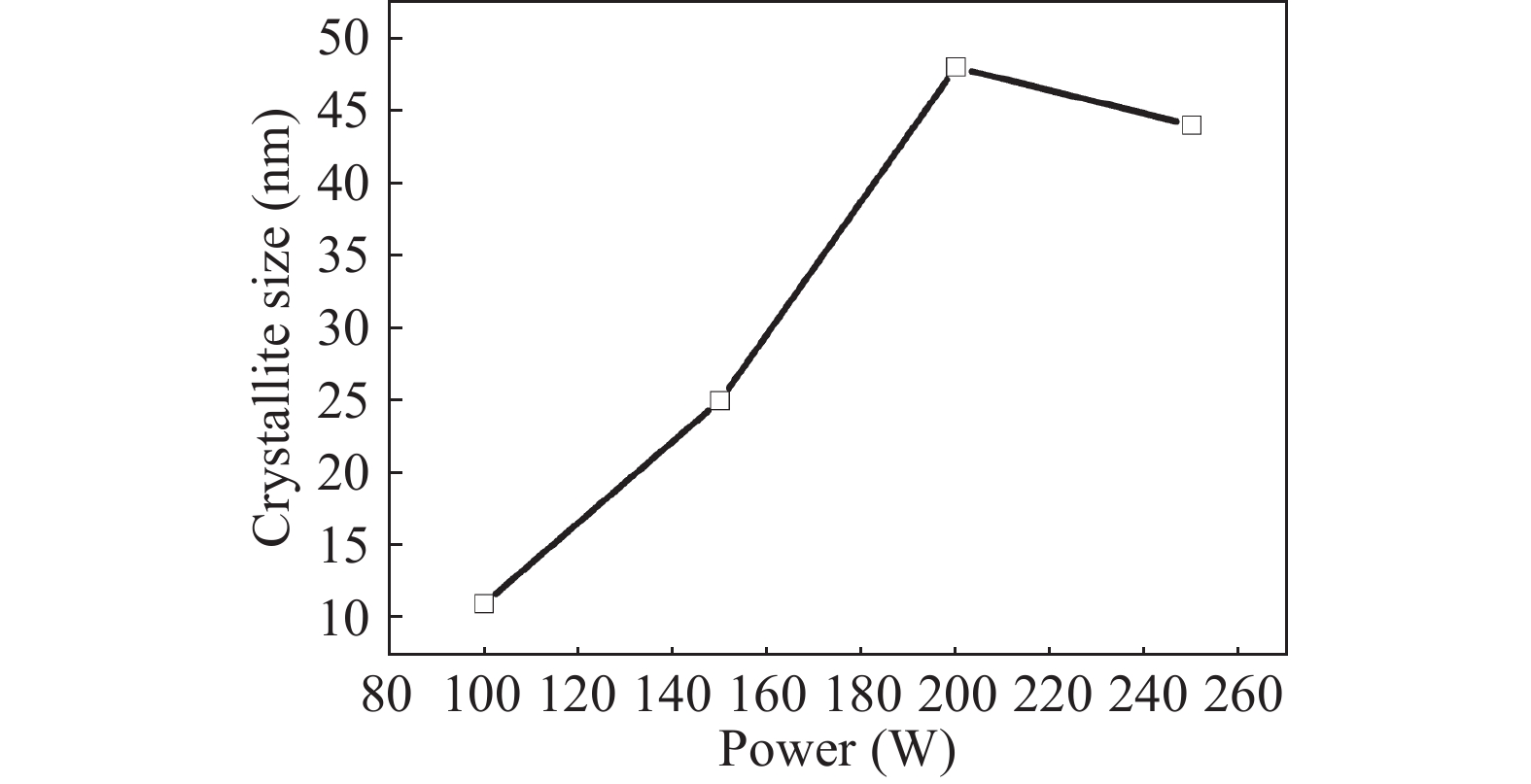
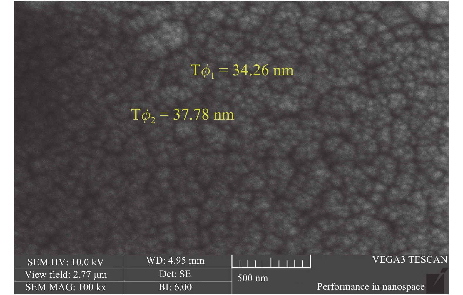
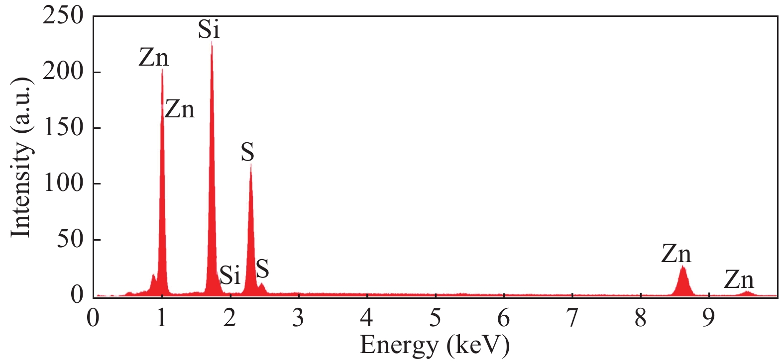
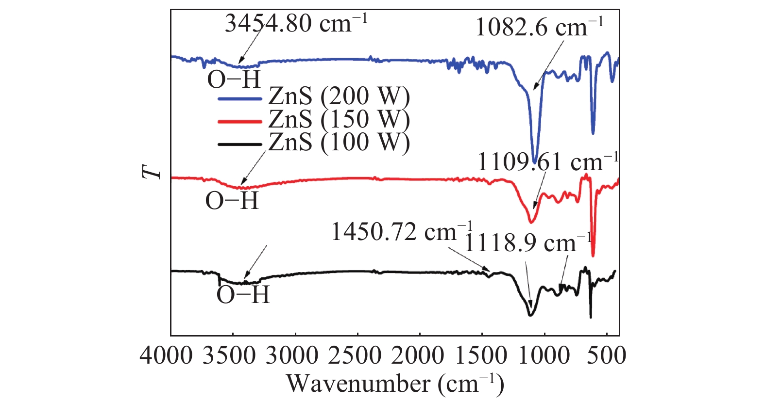
Zinc sulphide (ZnS) thin films have grown on glass and Si substrates by reactive cathodic radio frequency (RF) sputtering. The RF power was varied in the range of 100 to 250 W, while the deposition time is set at 75 min. The optical, structural, and morphological properties of these thin films have been studied. The optical properties (mainly thickness, refractive index, absorption coefficient, and optical band gap) were investigated by optical transmittance measurements in the wavelength range of ultraviolet-visible-near infrared spectroscopy and spectroscopy infrared with Fourier transform. Fourier (FT-IR) and XRD analysis indicated that all sputtering ZnS films had a single-phase with a preferred orientation along the (111) plane of the zinc sphalerite phase (ZB). The crystallite size ranged from 11.5 to 48.5 nm with RF power getting a maximum of 200 W. UV–visible measurements exhibited that the ZnS film had more than 80% transmission in the visible wavelength region. In addition, it has been observed that the band gap energy of ZnS films is decreased slightly from 3.52 to 3.29 eV, and as the RF power is increased, the film thickness increases with the speed of deposit growth. Scanning electron microscopy observations revealed the types of smooth-surfaced films. The measurements (FT-IR) revealed at wave number 1118 and 465.02 cm−1 absorption bands corresponding to the symmetrical and asymmetric vibration of the Zn–S stretching mode. X-ray reflectometry measurements of ZnS films have shown that the density of the films is (3.9 g/cm3) close to that of solid ZnS.


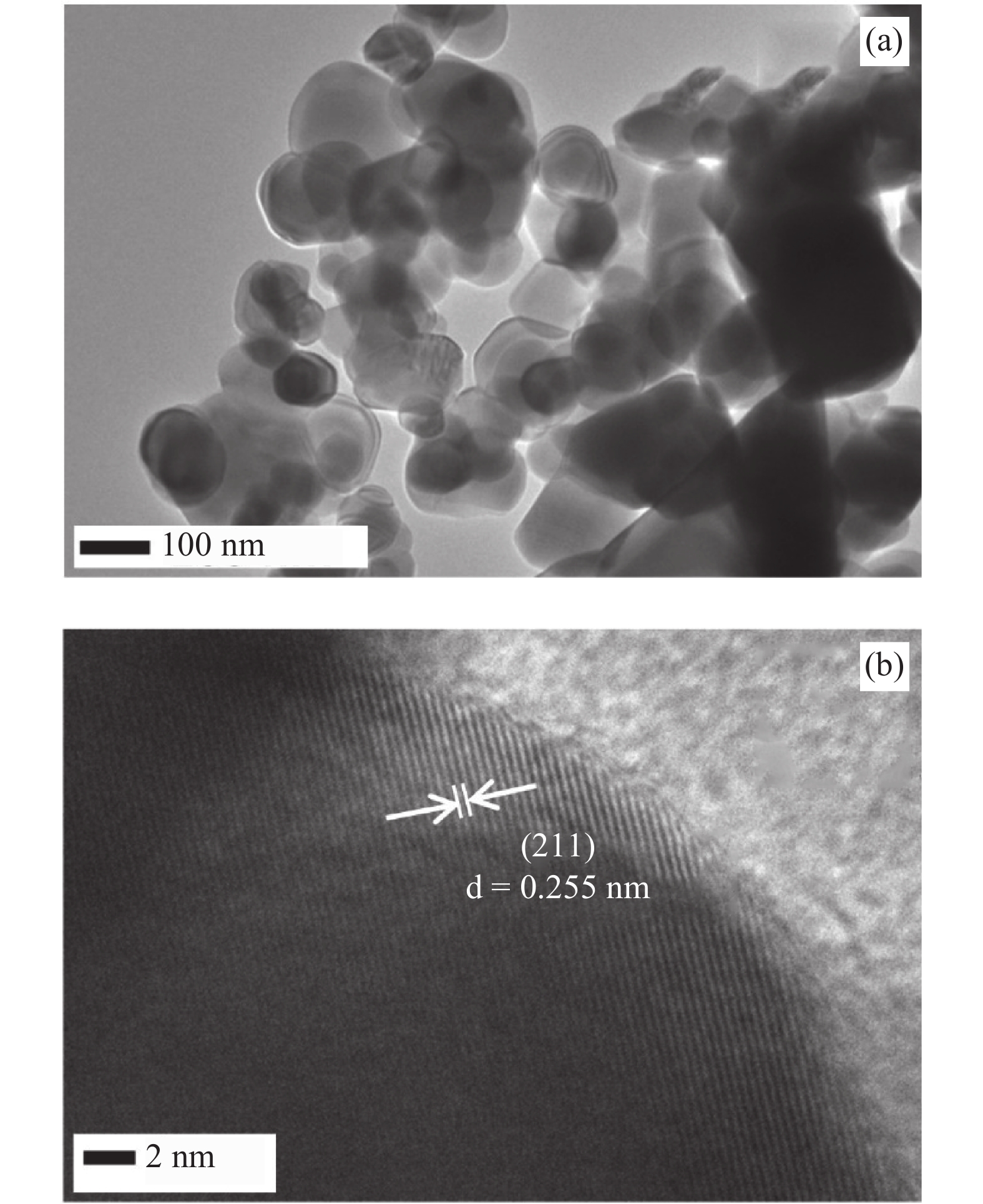
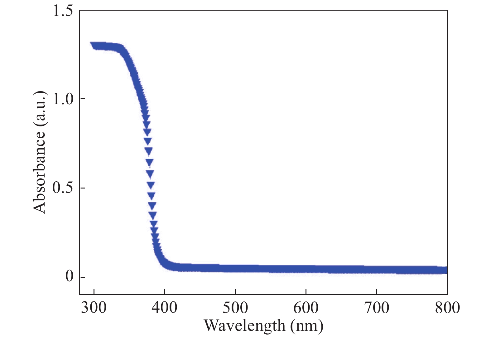
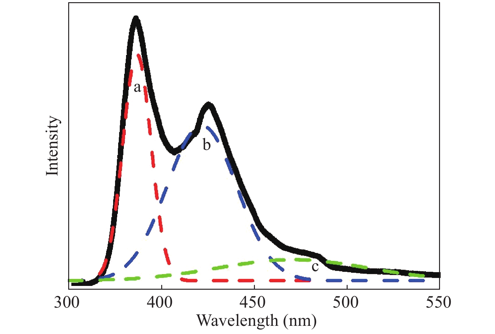
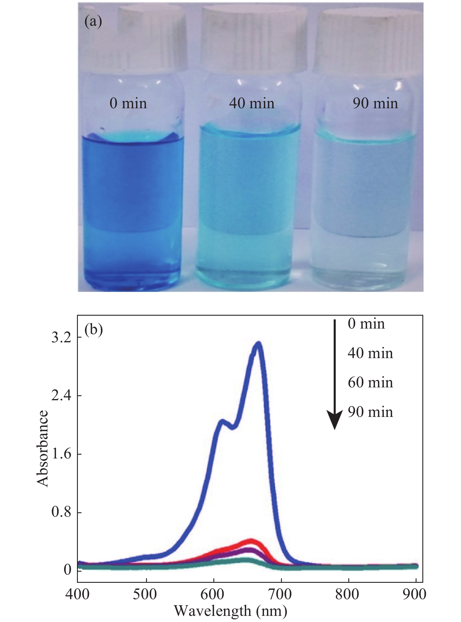
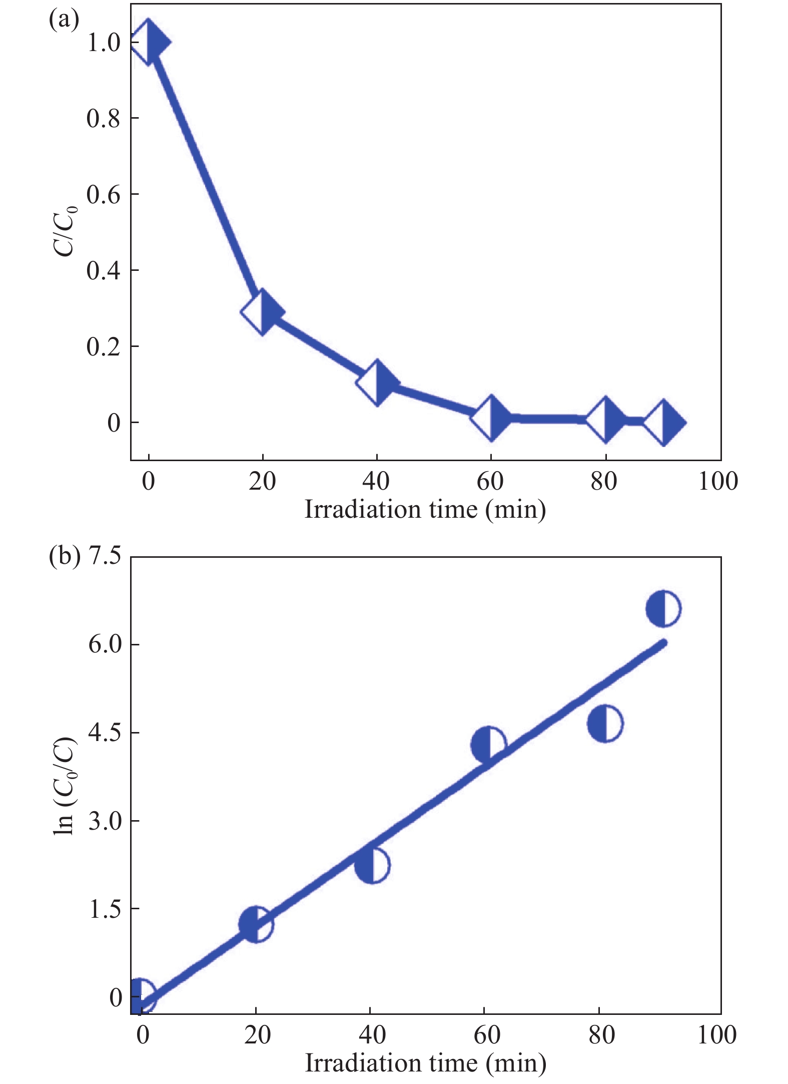
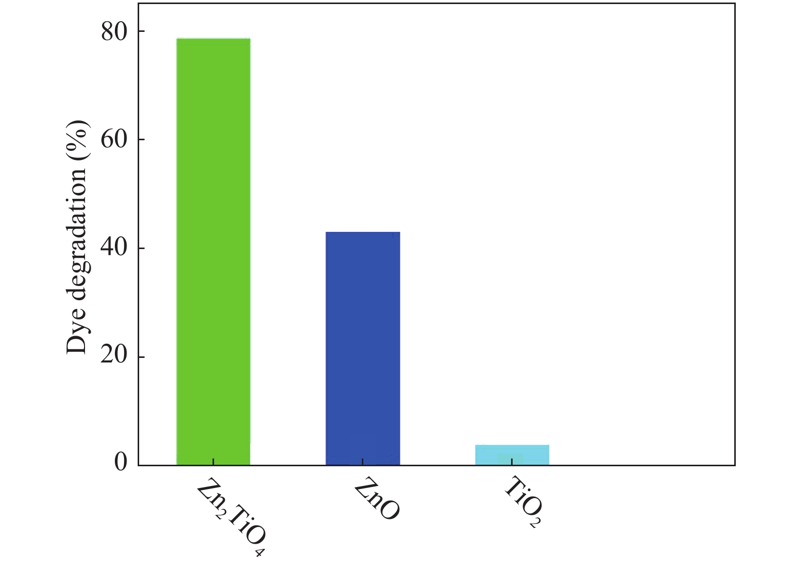
In this investigation, visible photocatalytic dye decomposition is carried out with compound semiconductor nanoparticles of zinc orthotitanate (Zn2TiO4). These nanoparticles were grown by the solid state reaction method and characterized by field emission scanning electron microscopy, transmission electron microscopy, X-ray diffraction, diffuse reflectance spectroscopy, photoluminescence study, and Brunauer–Emmett–Teller (BET) study. The BET surface area of the Zn2TiO4 nanoparticles was found to be 8.78 m2/g. The photocatalytic activity is carried out by using a 500 W halogen light source having a spectrum in the range of 450 to 860 nm and the reaction kinetics was found to be the pseudo first order. The reaction rate constant was found to be 0.069 min−1. Discussion is given on the possible mechanism of the observed visible photocatalytic dye decomposition activity. The cost of the material used is very low, so it could be very useful for visible photocatalytic dye decomposition.


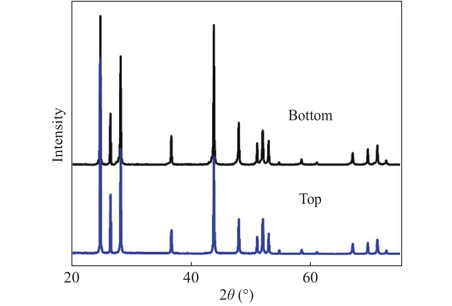
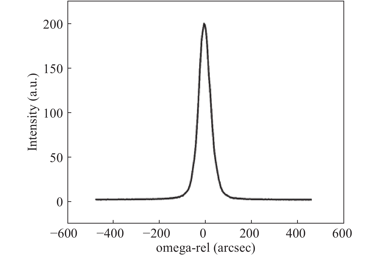
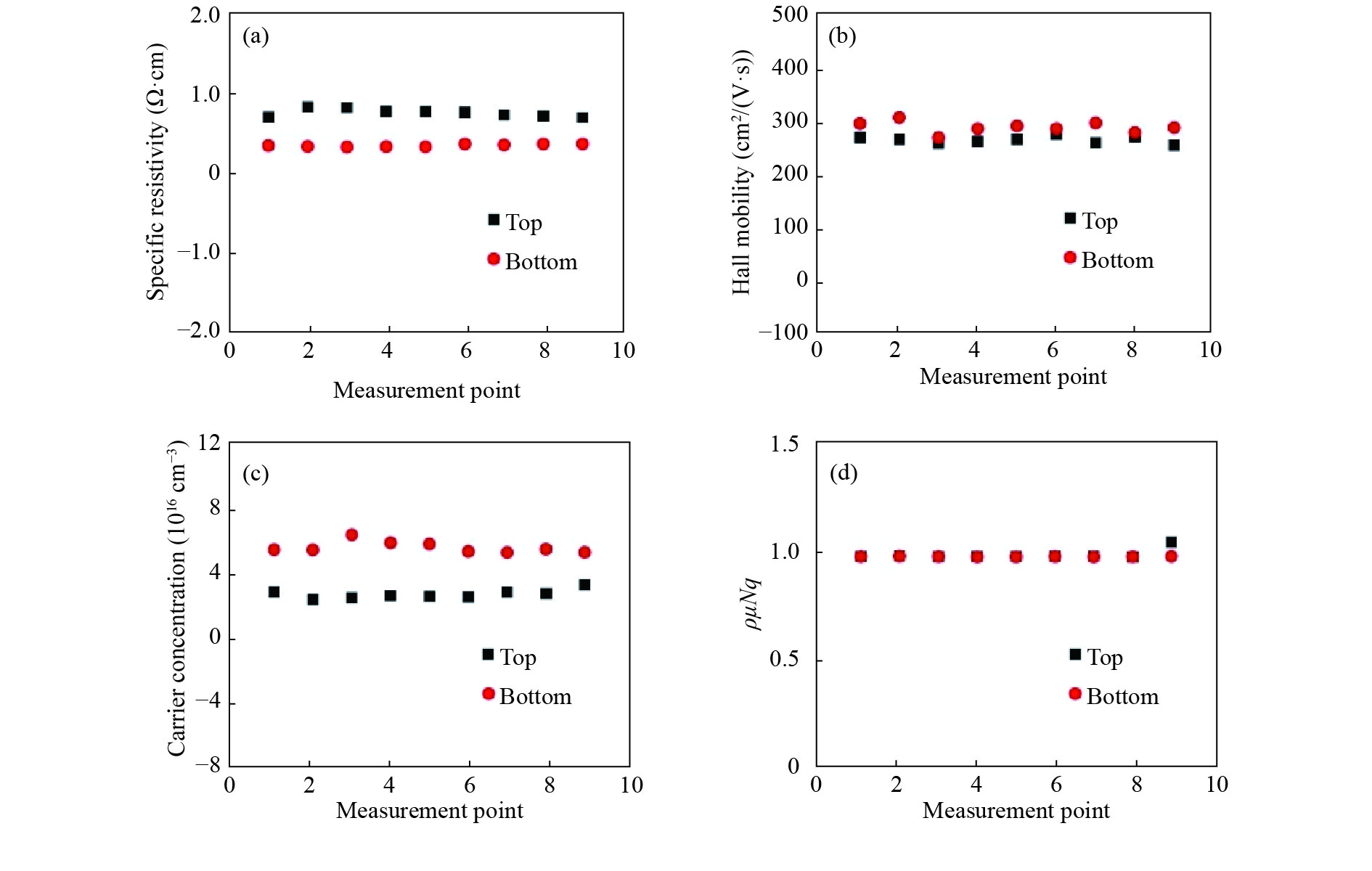
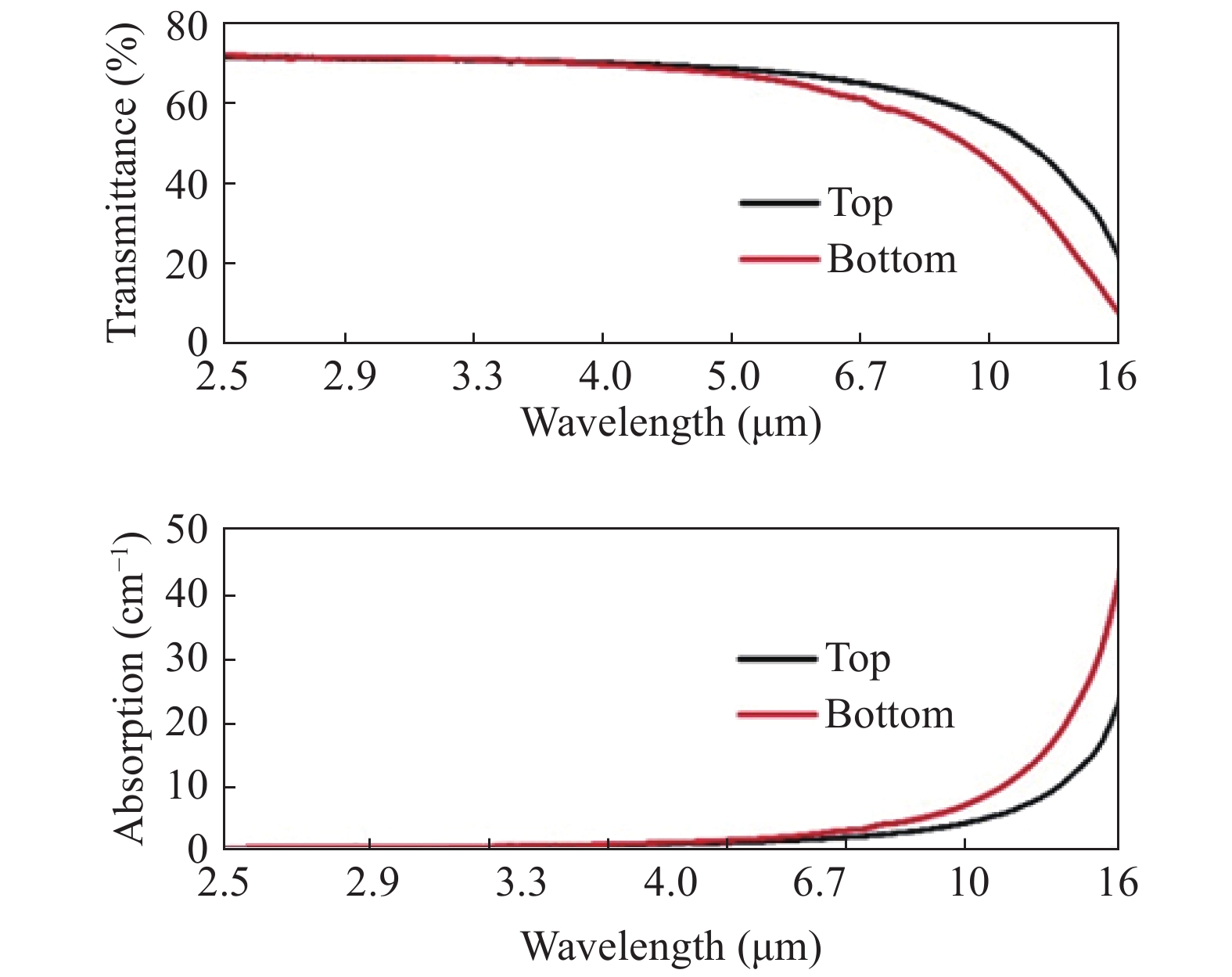
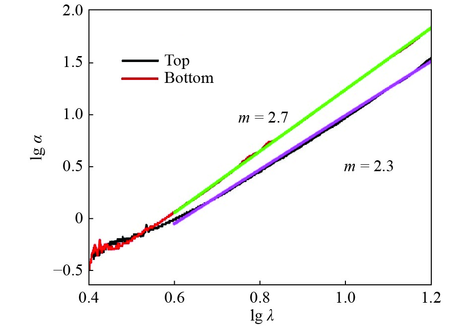
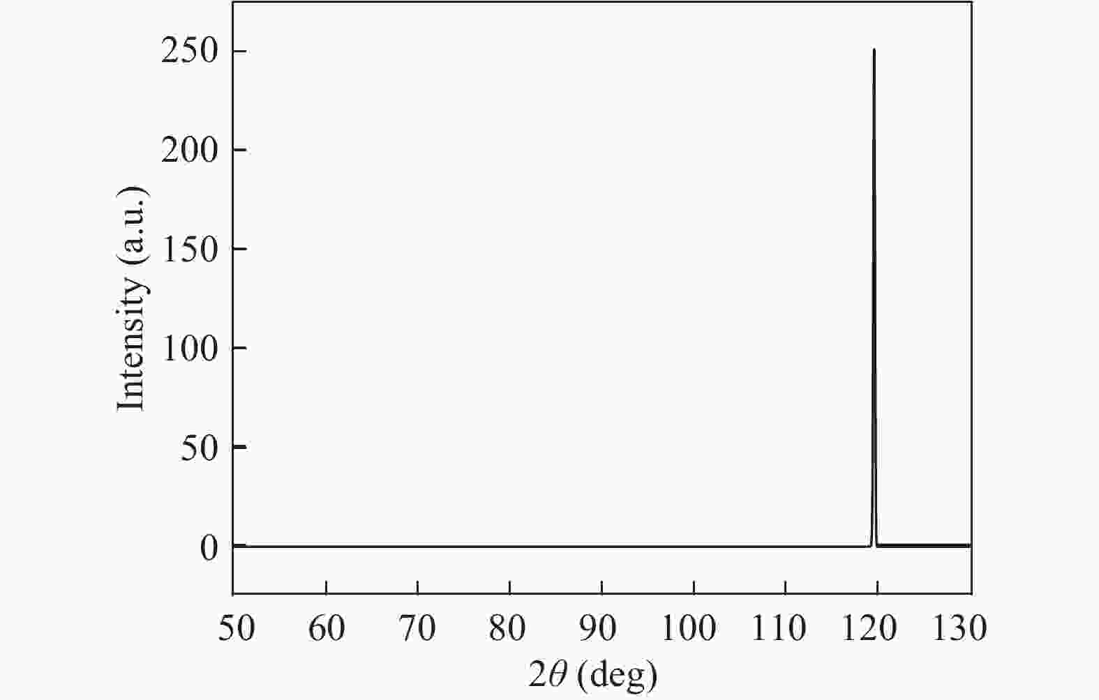
Φ55 × 15 mm2 CdS bulk single crystal with high infrared transmittance was grown by physical vapor transport. The single crystal has a consistent structure from top to bottom, which was confirmed by X-ray diffraction. The (002) full-width at half-maximum of the X-ray diffraction was measured to be 60.00 arcsec, indicating a good quality of the structure. Hall mobility, specific resistivity, and carrier concentration for the top and bottom of the crystal were observed as well. Transmittance for the CdS single crystal was measured to be higher than 70% from 2.5 to 4.5 µm, making the single crystal an important candidate for infrared window materials. Furthermore, the absorption mechanism of the CdS single crystal was analyzed.


We studied the effect of oxygen on the growth quality of diamond epitaxial layers. After oxygen is added during the growth of the diamond epitaxial layer, as the thickness of the epitaxial layer increases, the full width at half maximum of the rocking curve of the (004) plane of diamond epitaxial layer increases continuously, and, in addition, the intensities of both the Raman peaks and the free exciton emission peaks of the diamond epitaxial layer decrease continuously. These experimental results demonstrate that as the thickness of the diamond epitaxial layer increases, the quality of the diamond epitaxial layer degrades. The strong etching effect of the OH radical groups in the plasma on the diamond epilayers leads to the degradation of their crystallinity.


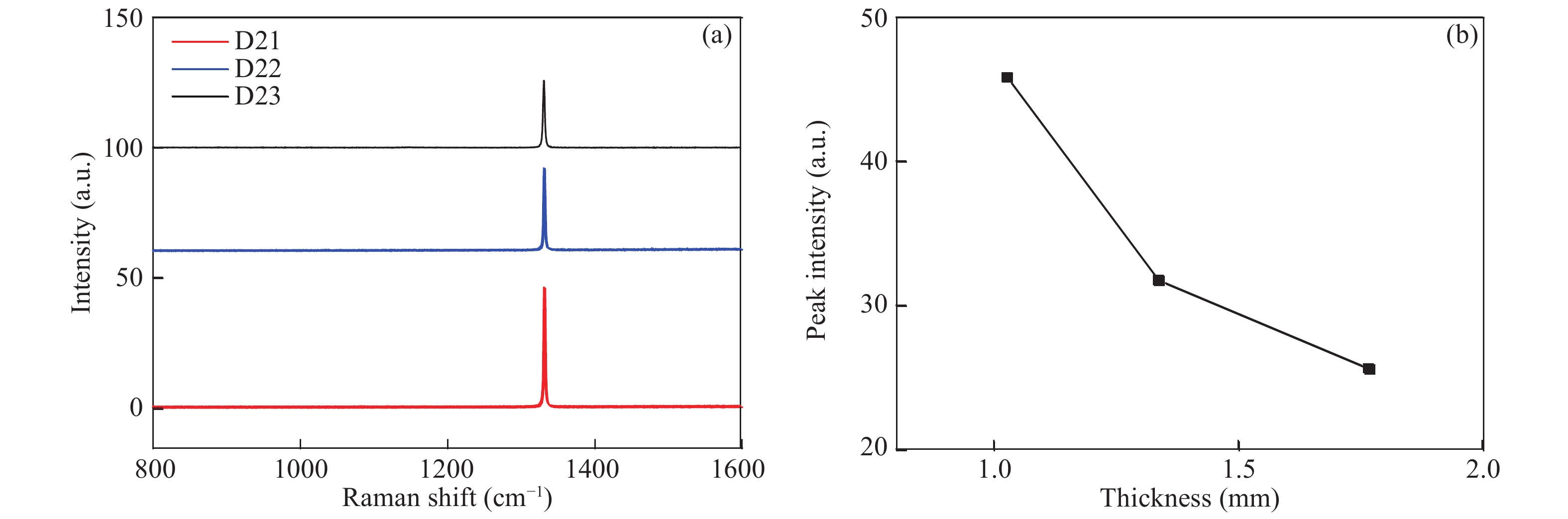


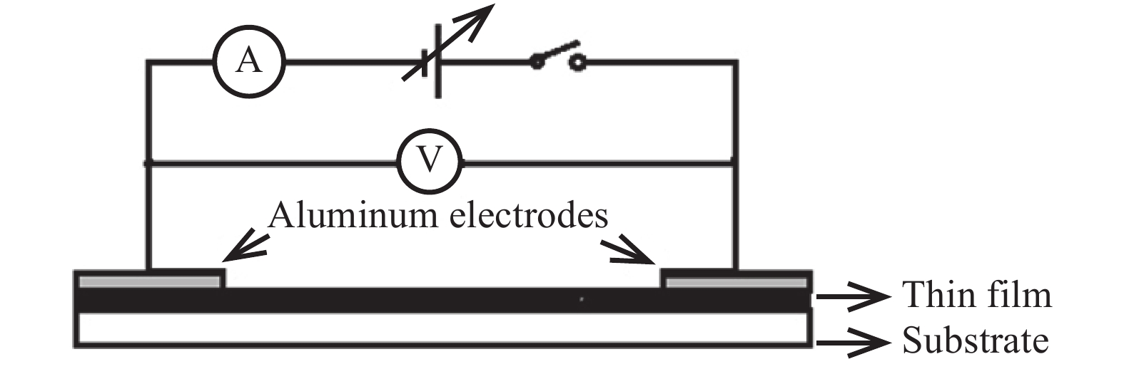
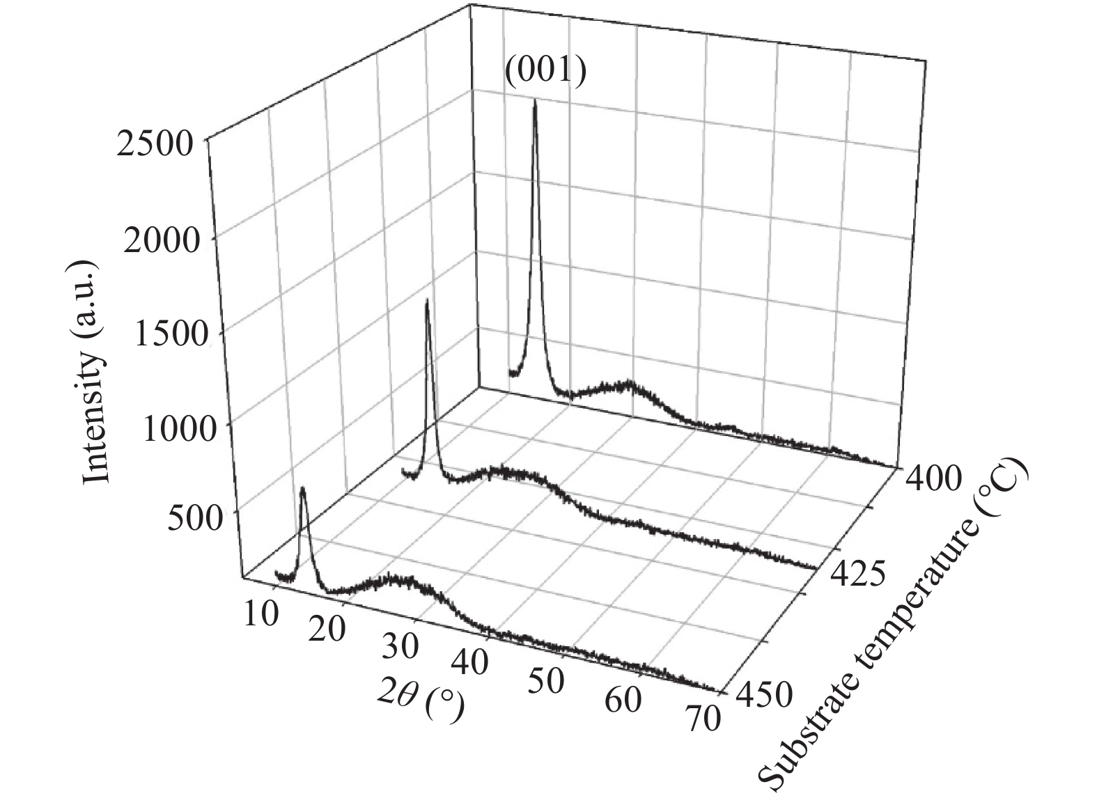
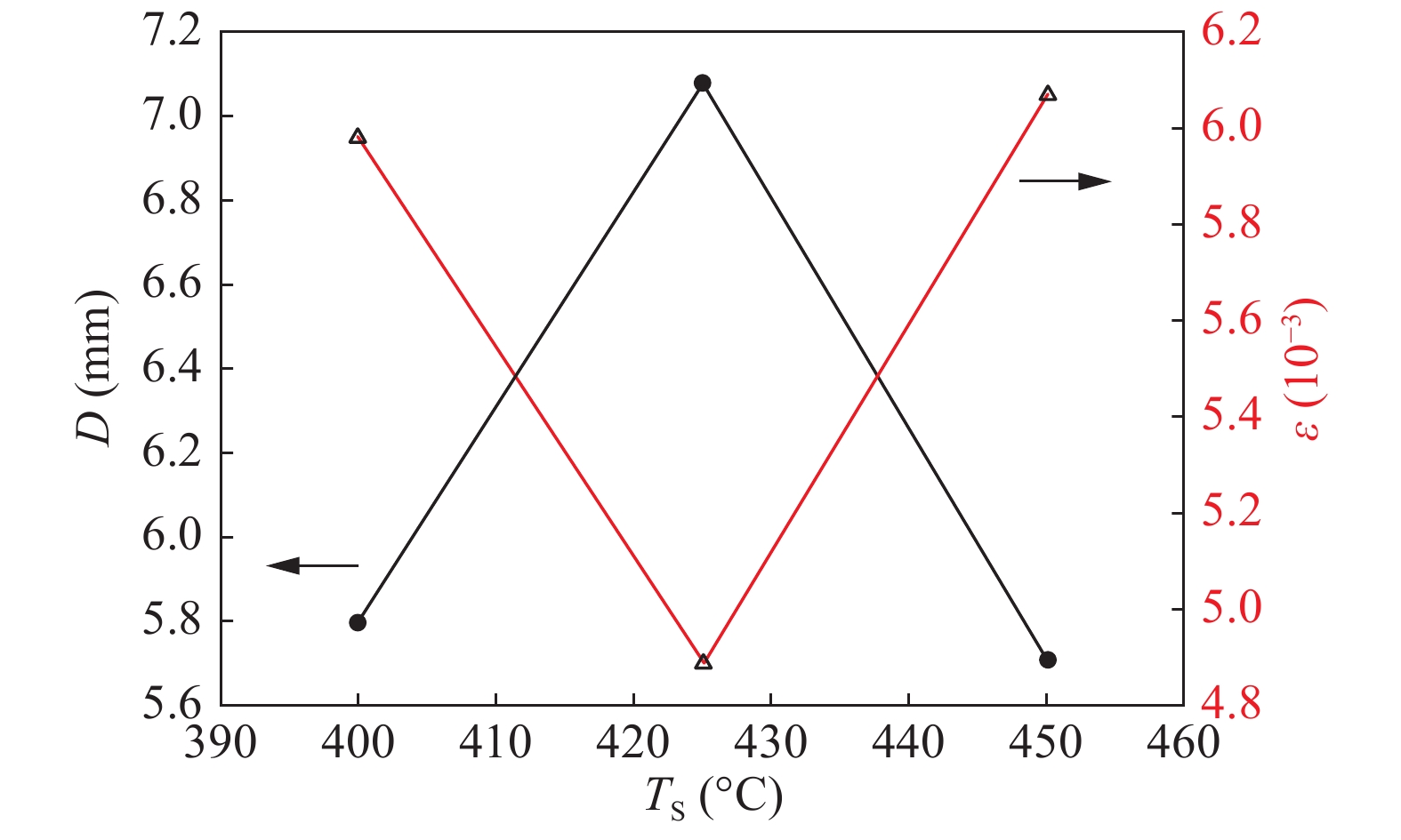
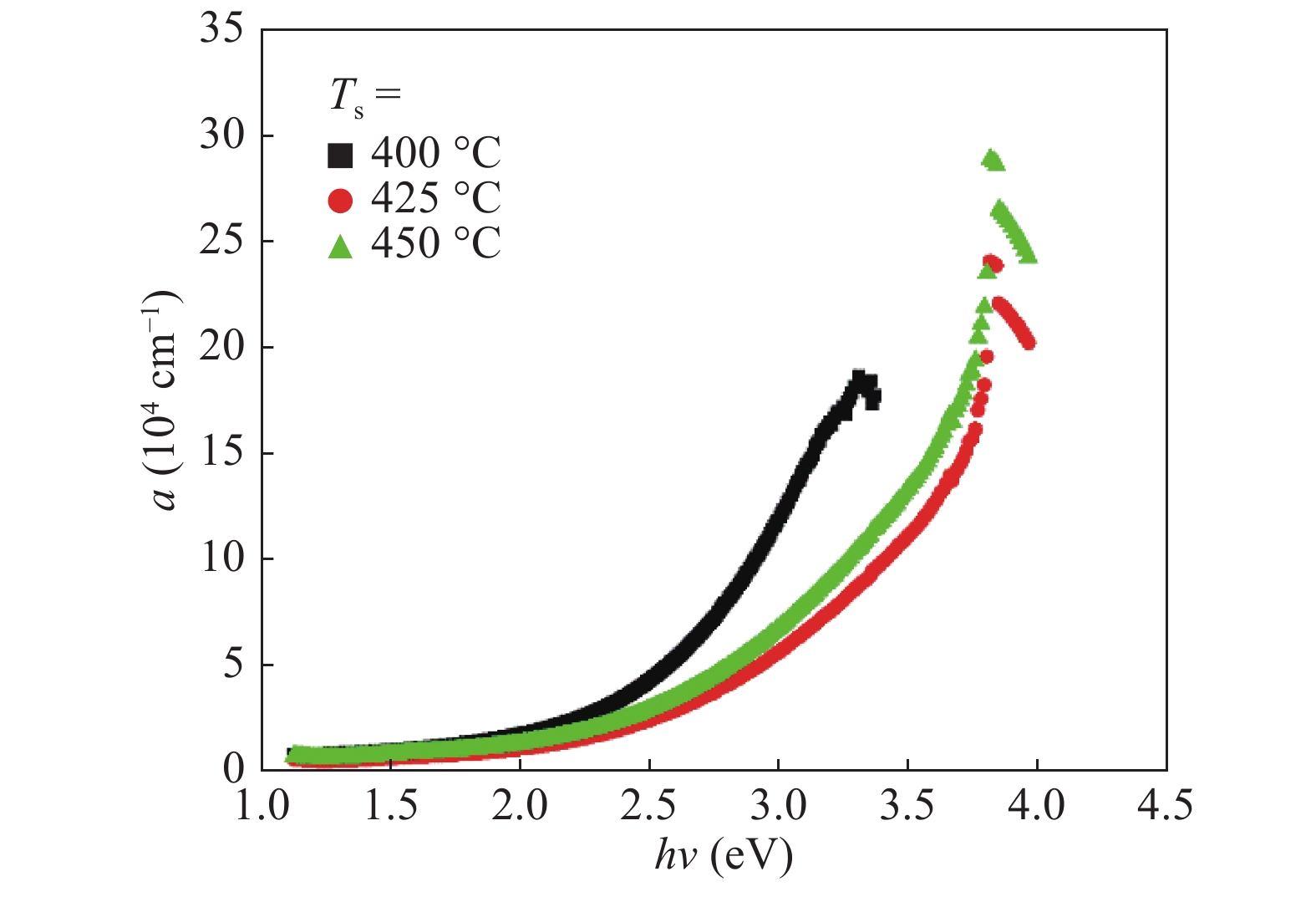
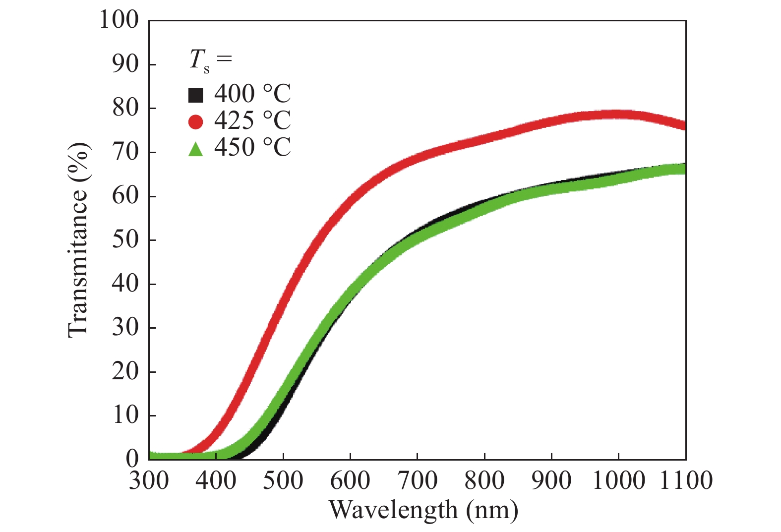
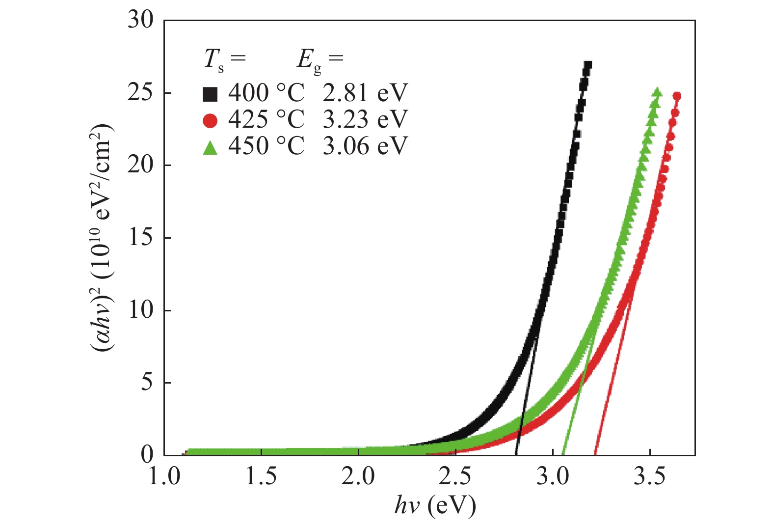
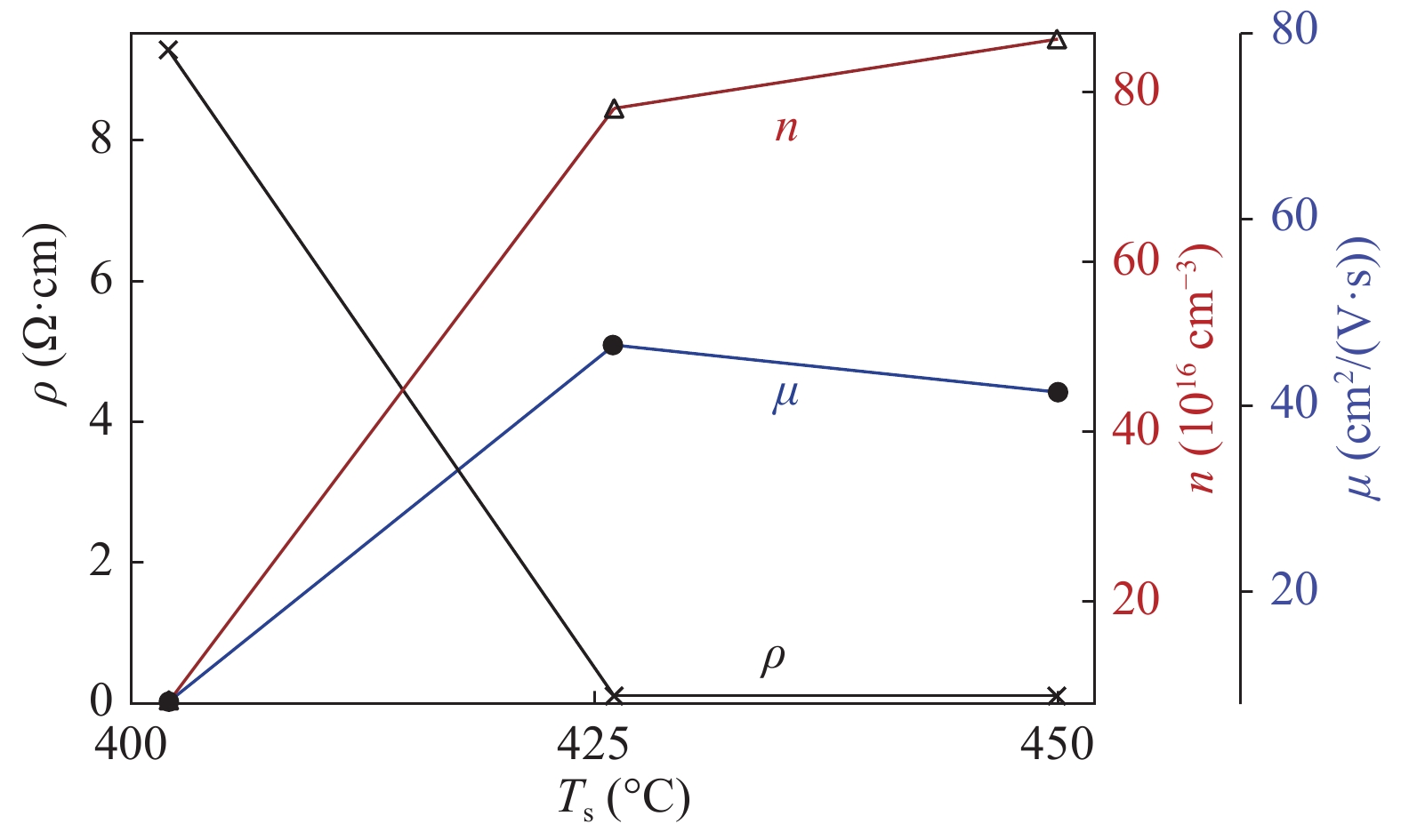
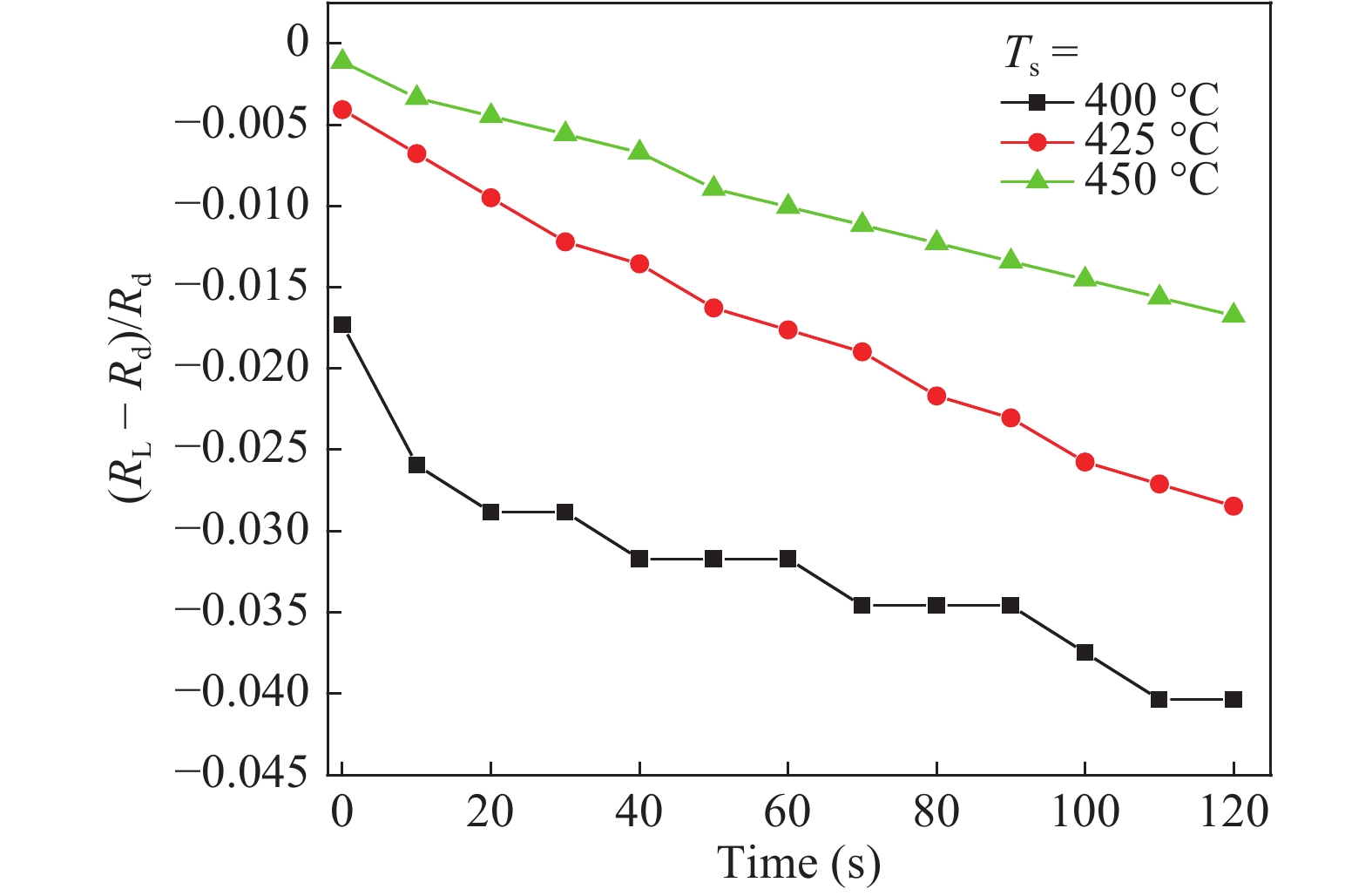
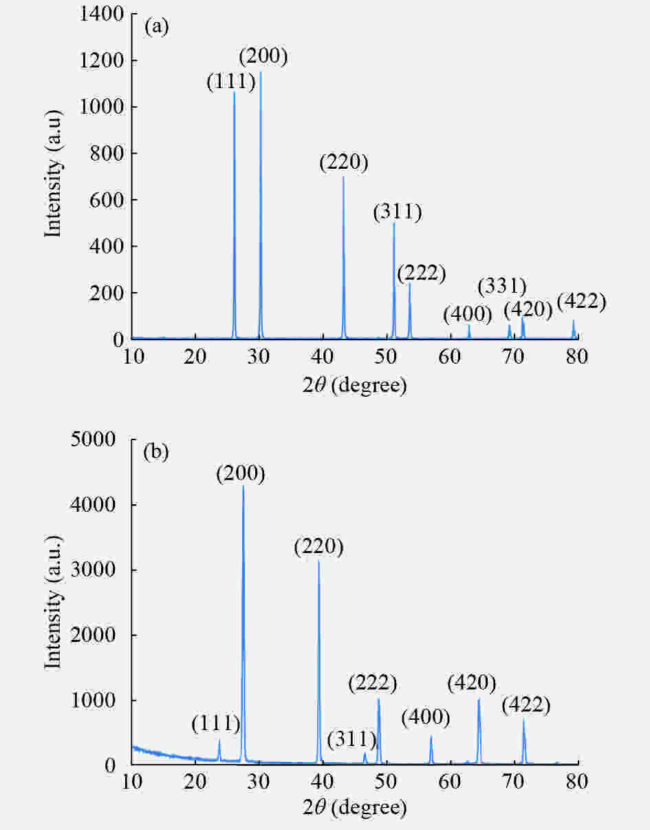
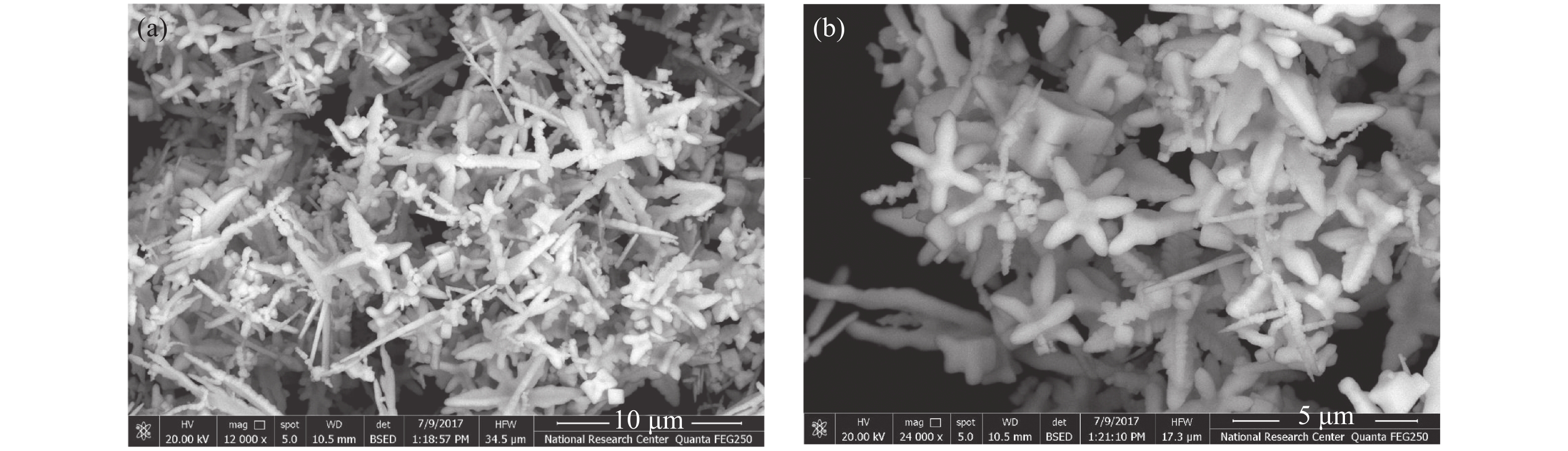
The main impetus of the present study is to investigate thin films of tin disulfide that have been doped with copper impurities and prepared on glass substrates by using the spray pyrolysis technique. Also, the influence of the substrate temperature on the structural, optical, and electrical properties of these films are investigated. The thin films have been characterized by X-ray diffraction (XRD), scanning electron microscopy (SEM), and optical absorption (UV–vis) analyses. The XRD patterns clarify that the thin films possess polycrystalline structures, having a peak associated with the (001) plane of the SnS2 phase. The average crystalline grain sizes were estimated to be within the range 5.7–7.1 nm. The SEM images indicate that the grain size increases from 53 to 114 nm with an increment in the substrate temperature, resulting in an increasing–decreasing trend in the band gap of the thin films. However, the films’ resistance decreases from 92.5 to 0.174 Ω·cm as the substrate temperature increases from 400 to 450 °C. Also, their optical energy band gap depicts an increasing–decreasing trend with the estimated values of 2.81, 3.21, and 3.06 eV at 400, 425, and 450 °C, respectively. The thin films exhibit n-type conductivity.

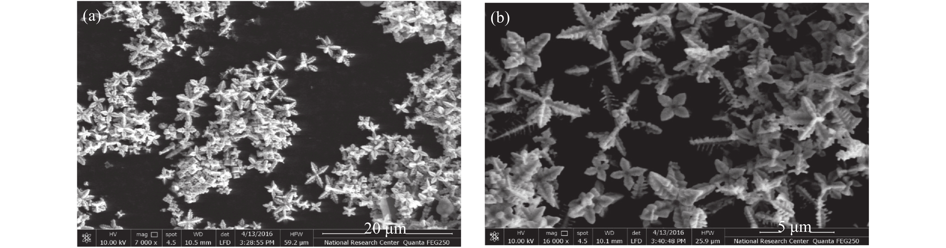
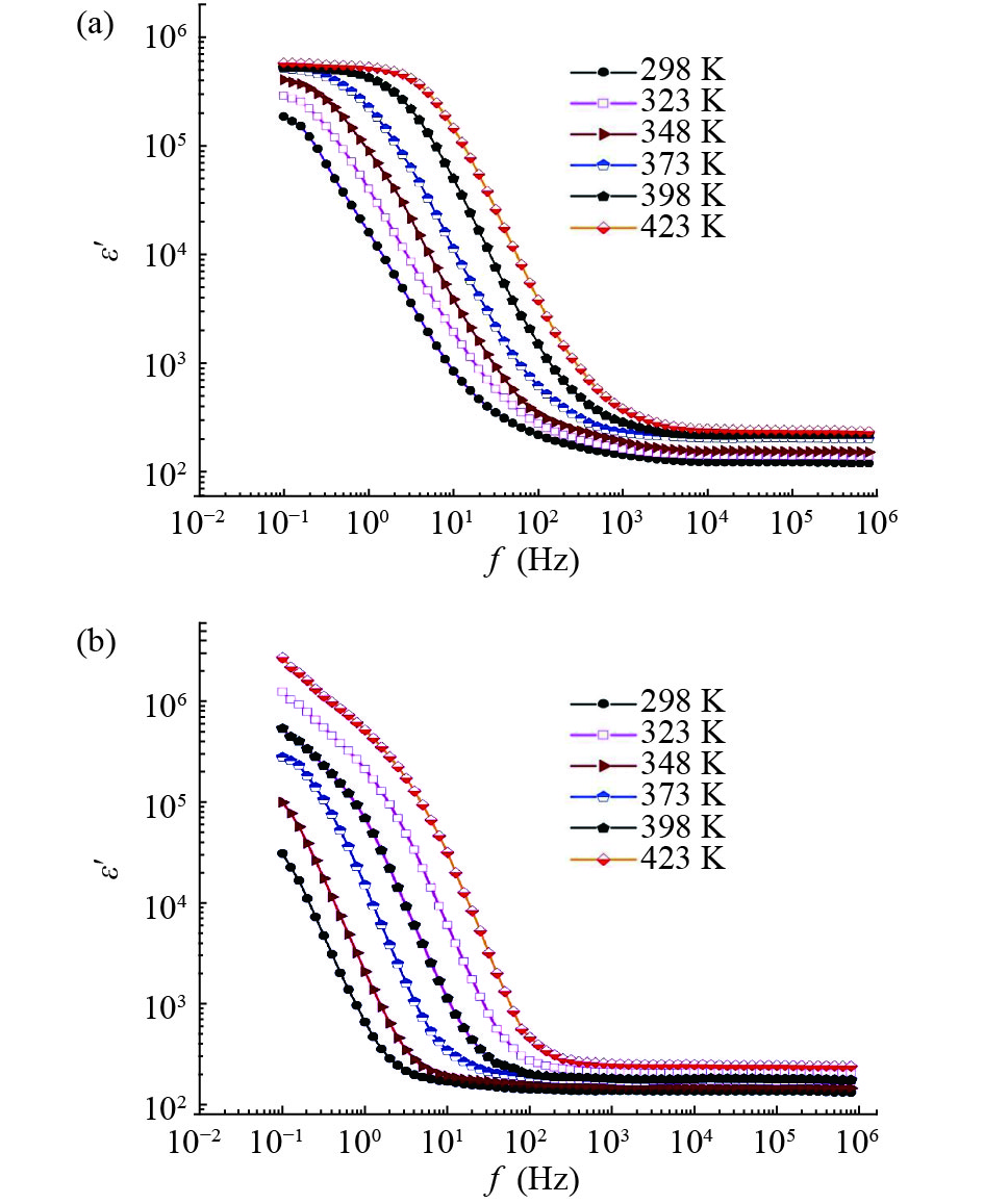
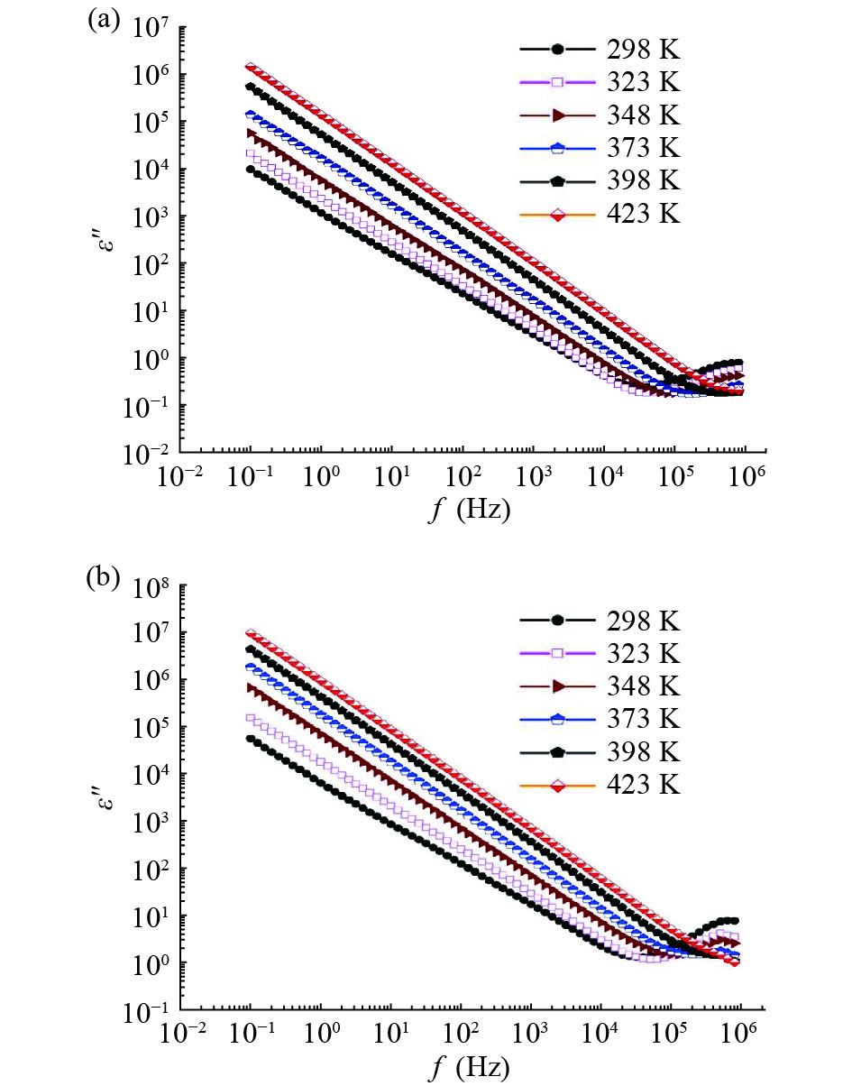
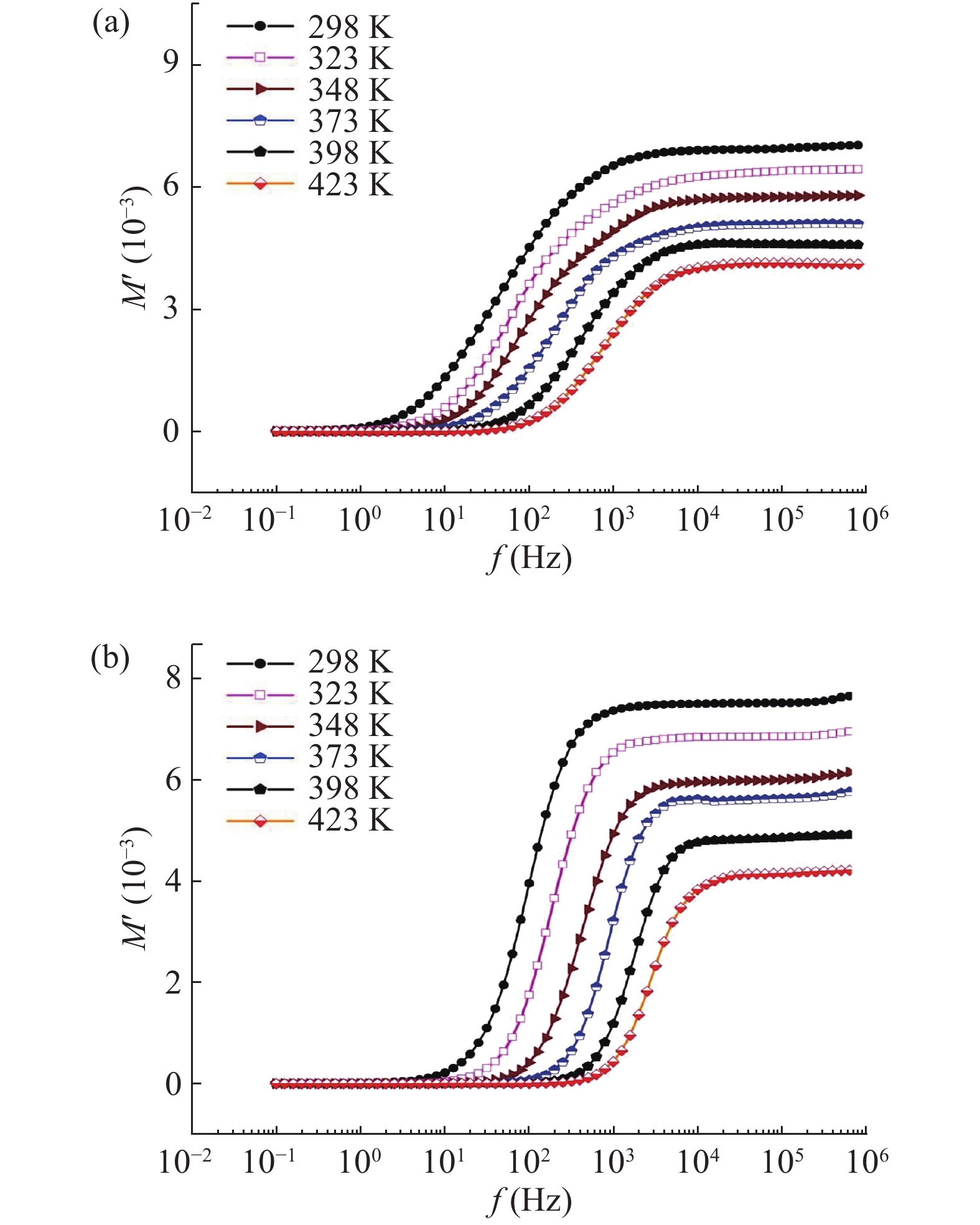
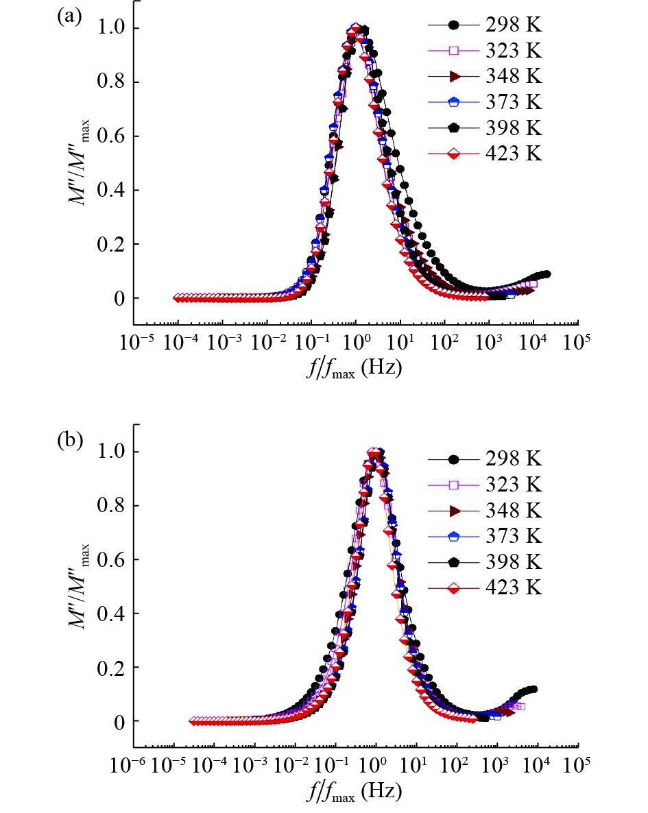
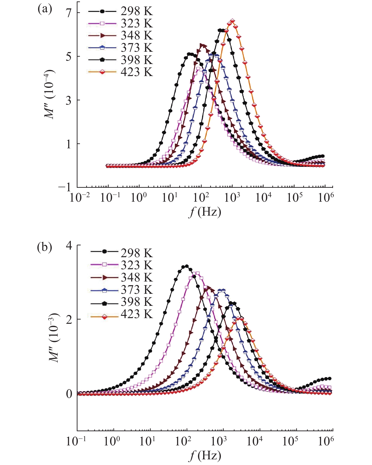
In this work, PbS and PbTe nanomaterials with various morphologies were synthesized by a hydrothermal method. The structural properties were investigated by using X-ray diffraction (XRD) and corresponding scanning electron microscopy together with their EDX analysis. Both the PbS and PbTe nanomaterials possess good polycrystalline structure. The crystallite size, determined from the XRD data, of PbS is 5 nm whereas the corresponding value of PbTe is 2.69 nm. SEM micrographs reveal that the prepared PbS nanomaterial has star-shaped structures, micro-flowers, some cubes, and semi-dendrites, whereas PbTe has semi-flower structures. Additionally, the dielectric properties have been studied in a broad frequency range from 0.1 Hz up to 1 MHz at temperatures from 298–423 K. The real and imaginary parts of the complex dielectric constant ε' and ε'' of PbTe are comparatively higher than those of PbS. Moreover, the dielectric data were analyzed on the basis of the electric modulus.


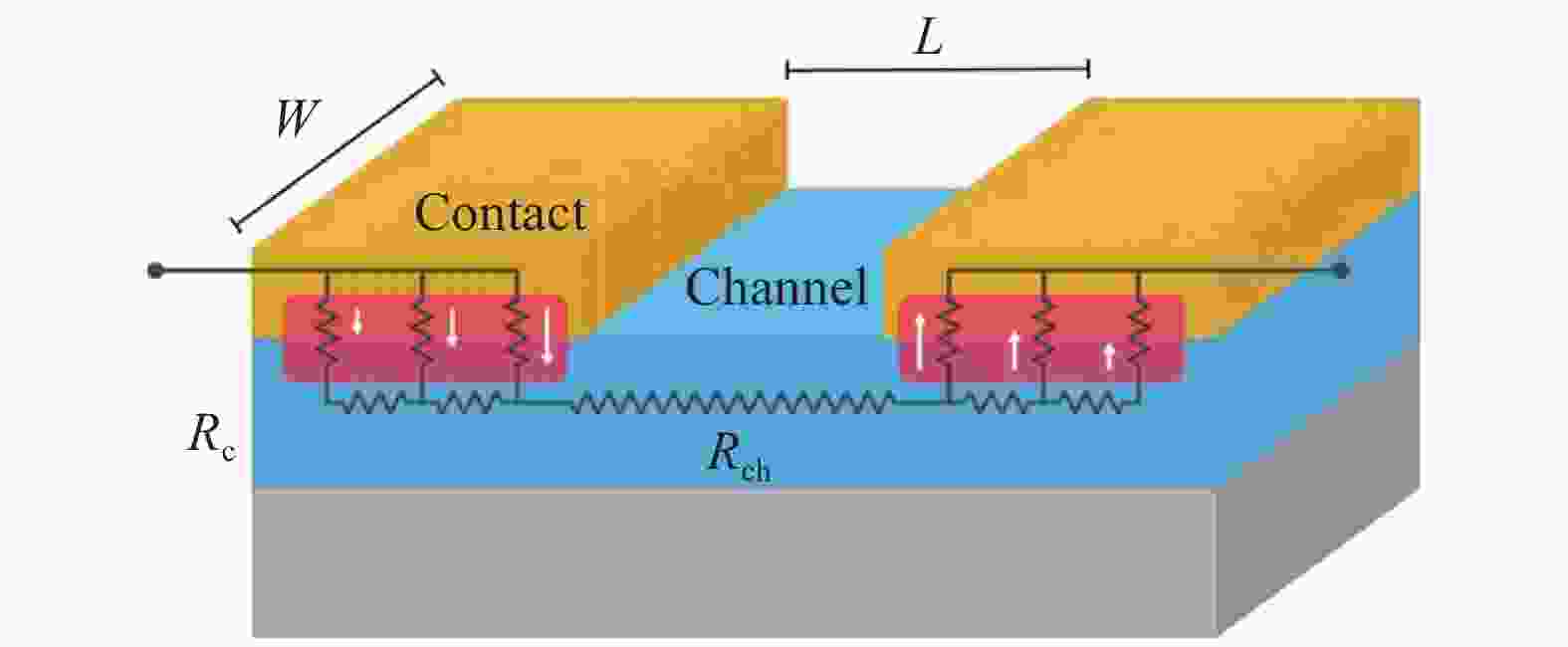
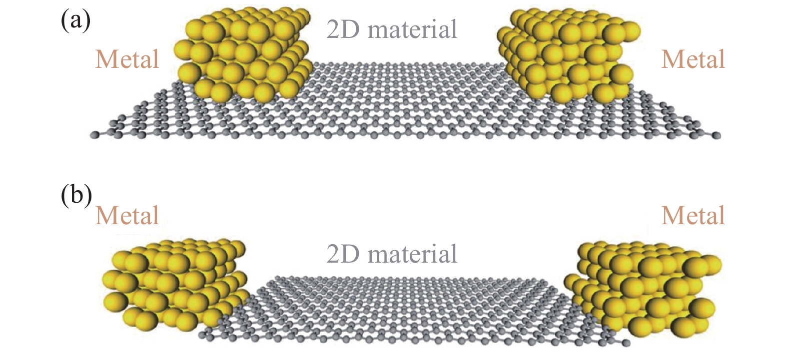
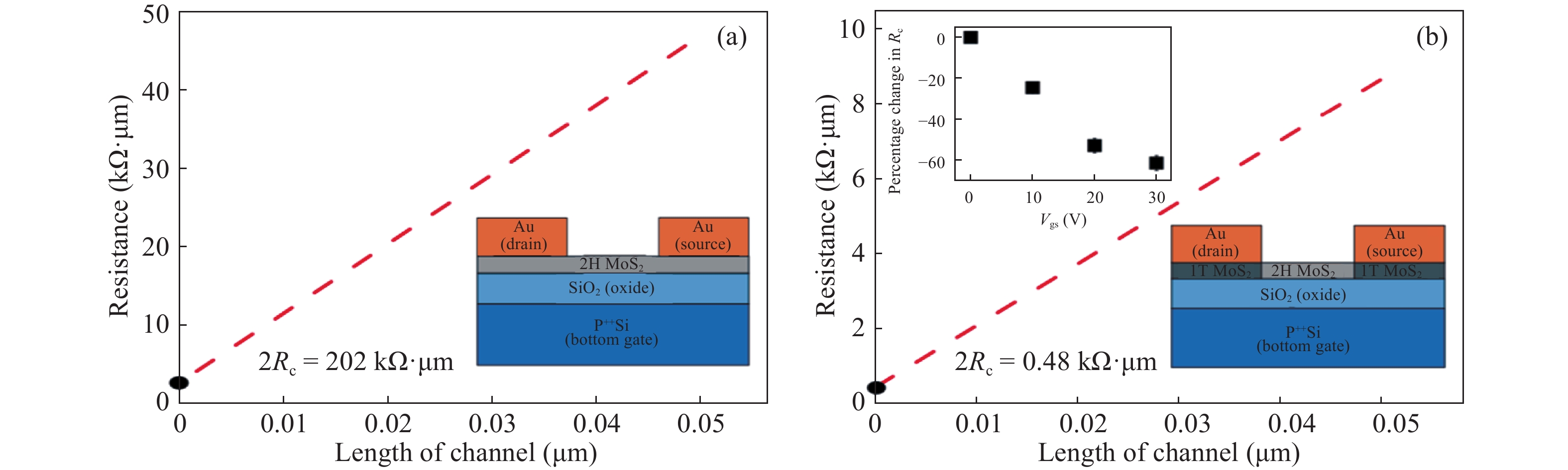
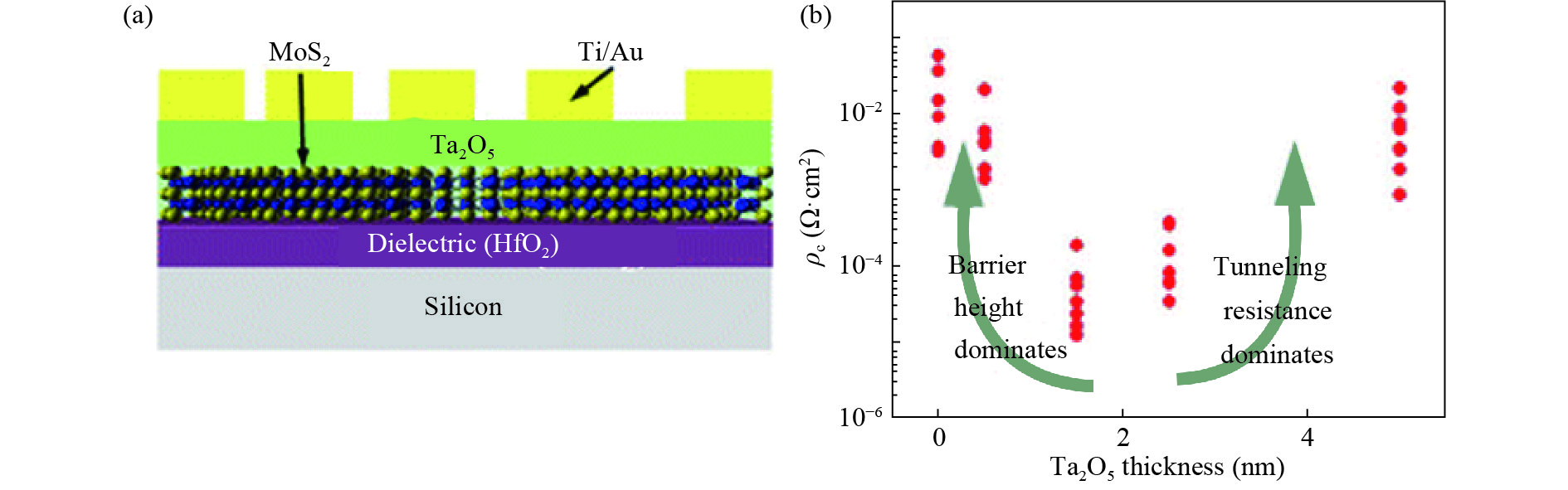
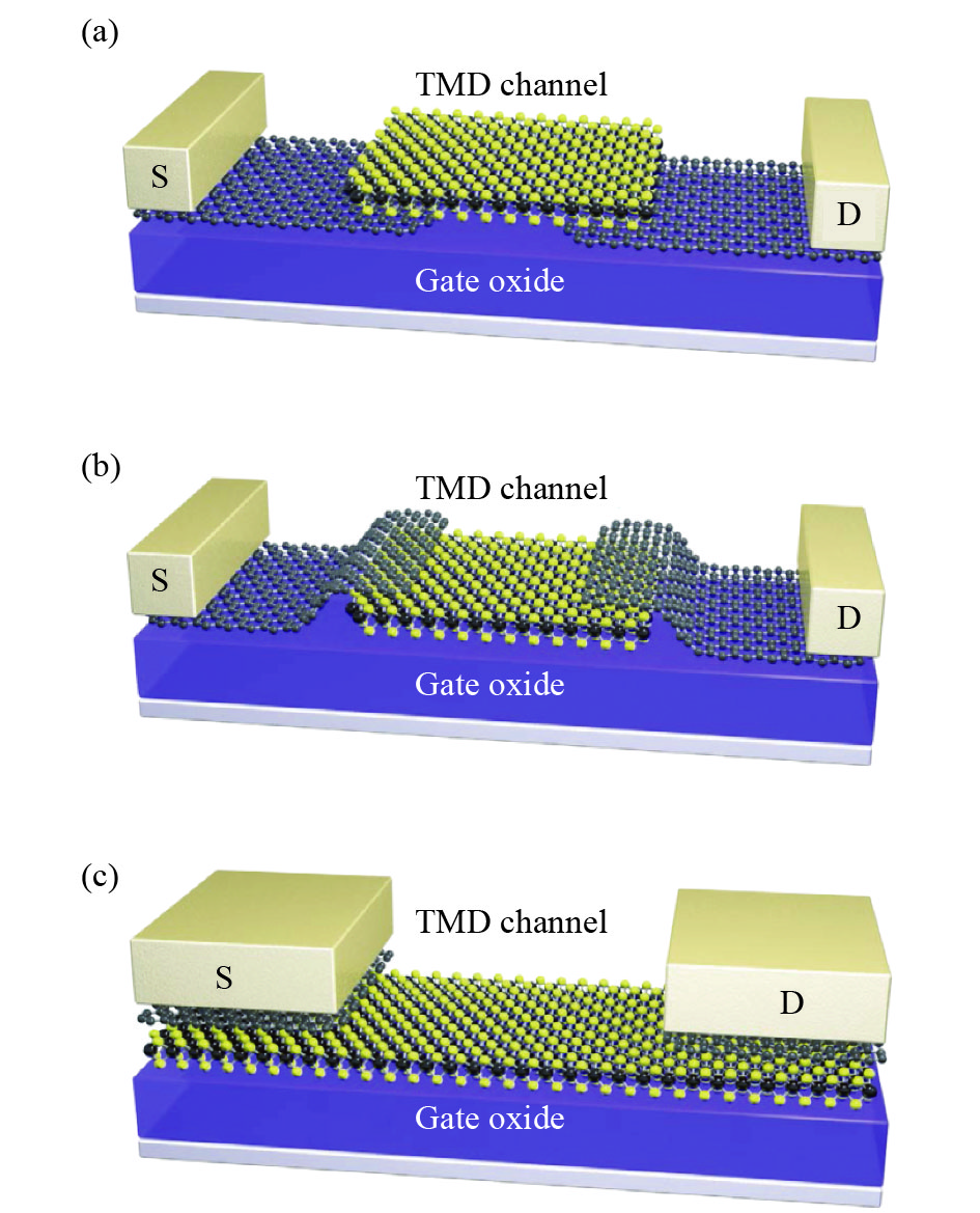
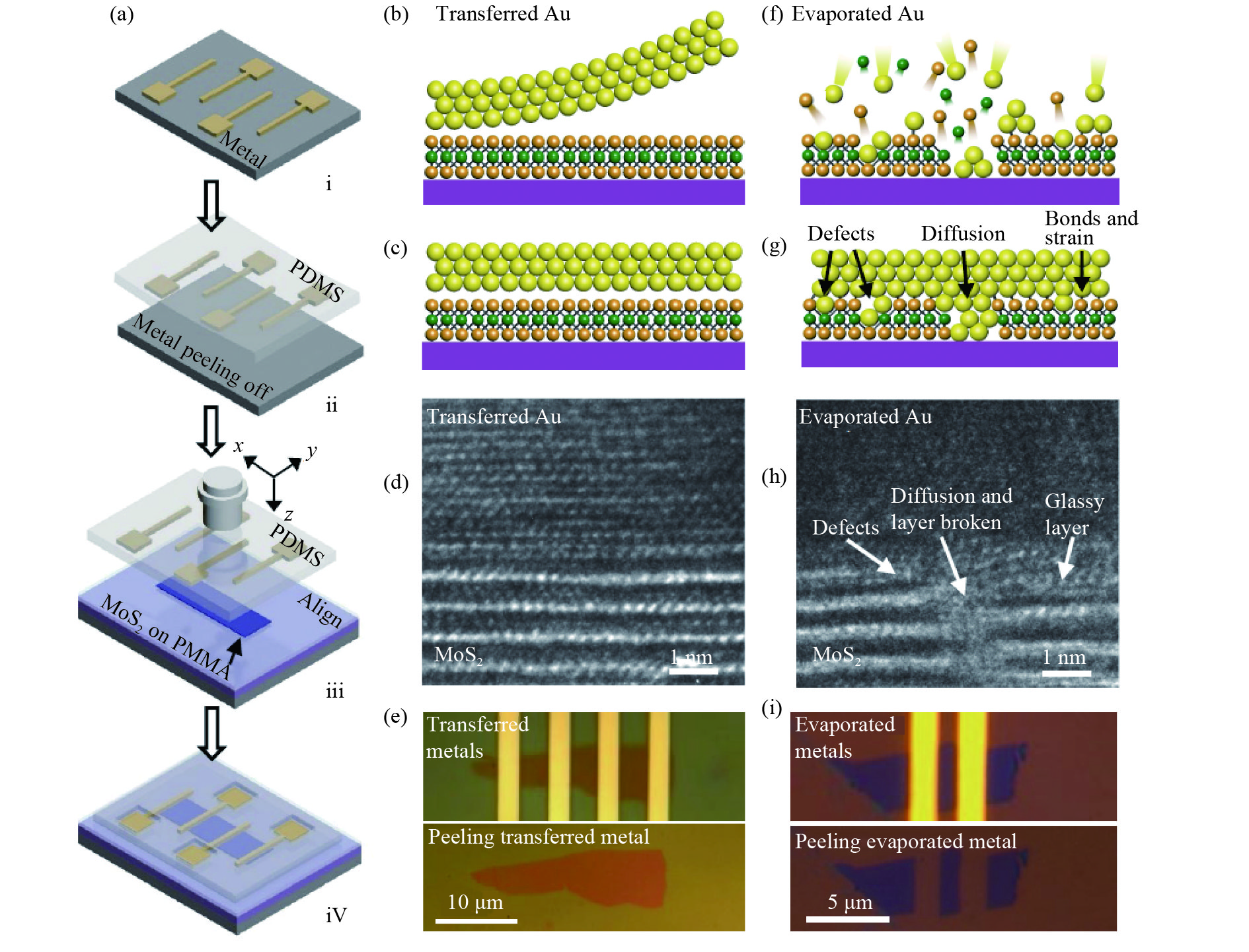
Two-dimensional (2D) transition-metal dichalcogenides (TMDCs) have attracted enormous interests as the novel channel materials for atomically thin transistors. Despite considerable progress in recent years, the transistor performance is largely limited by the excessive contact resistance at the source/drain interface. In this review, a summary of recent progress on improving electrical contact to TMDC transistors is presented. Several important strategies including topology of contacts, choice of metals and interface engineering are discussed.


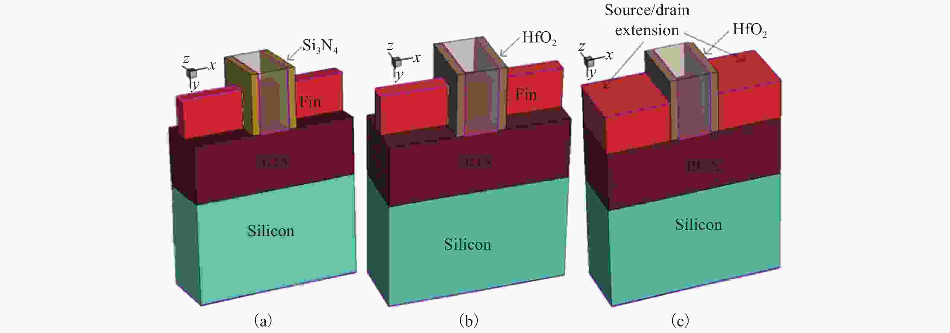
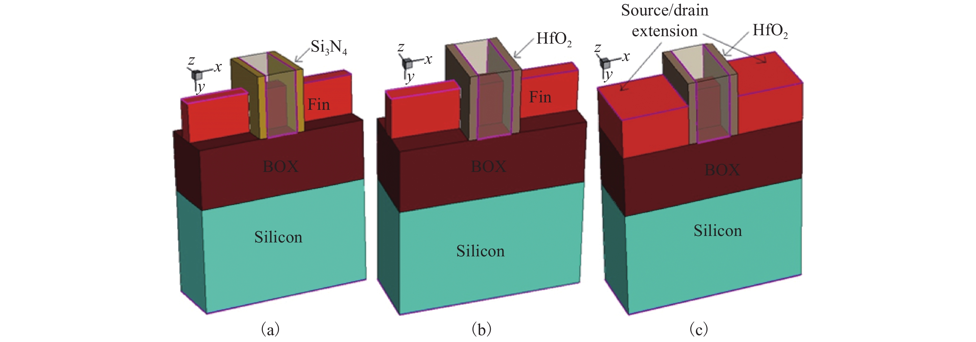
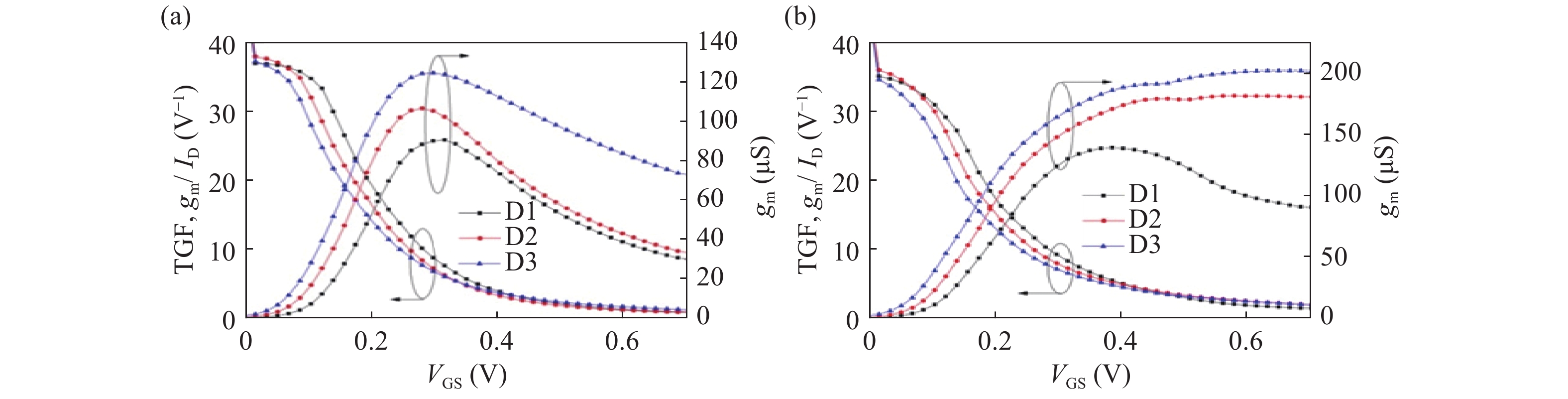
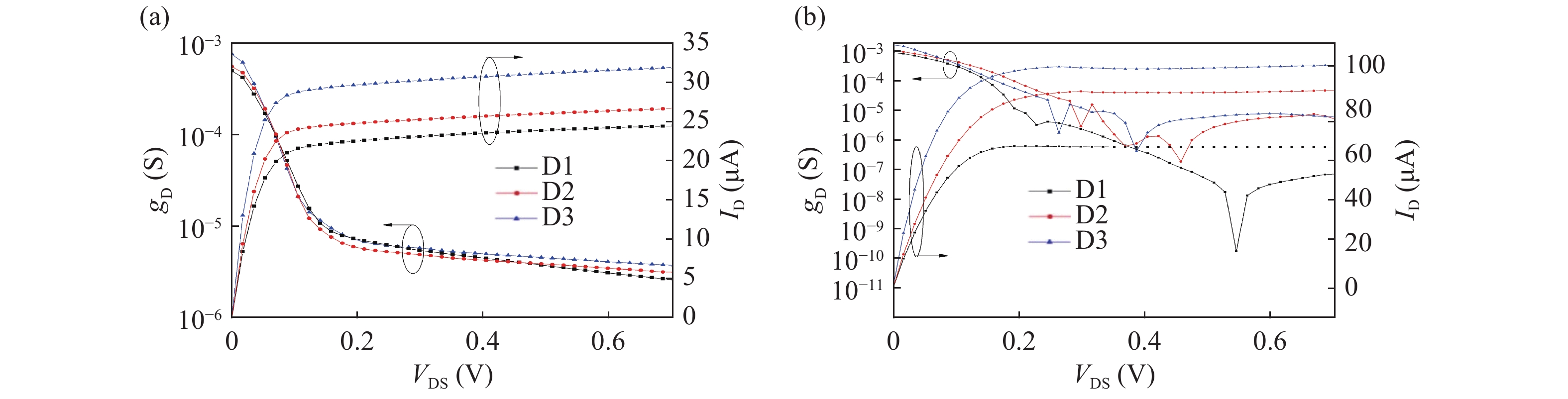
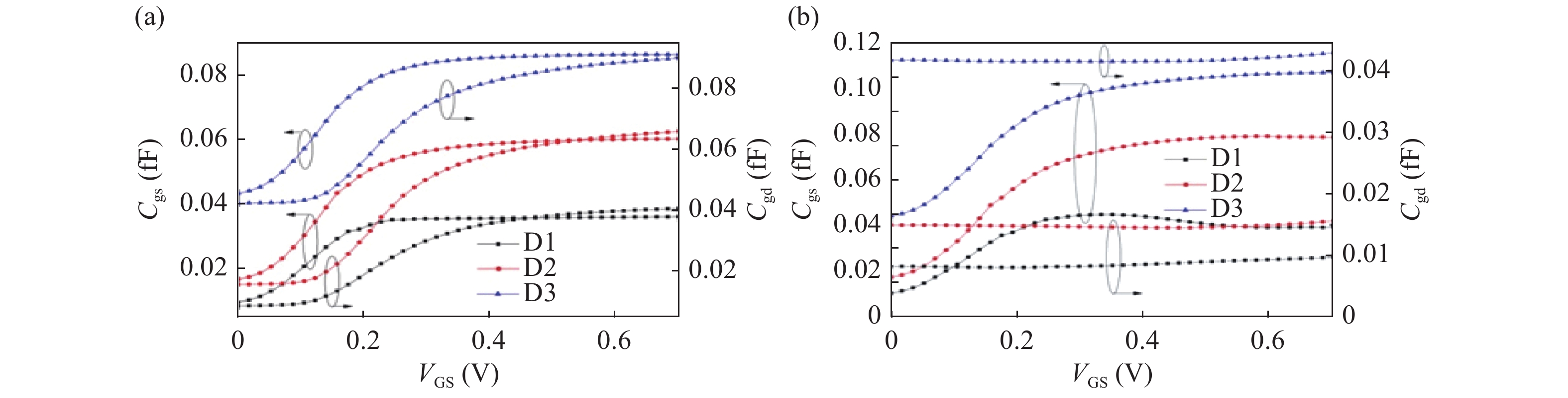
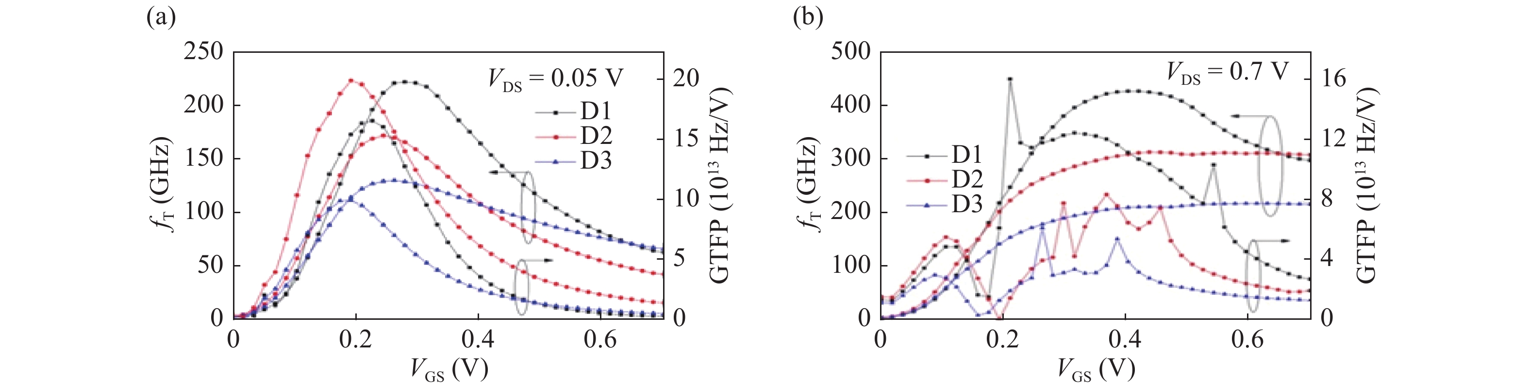
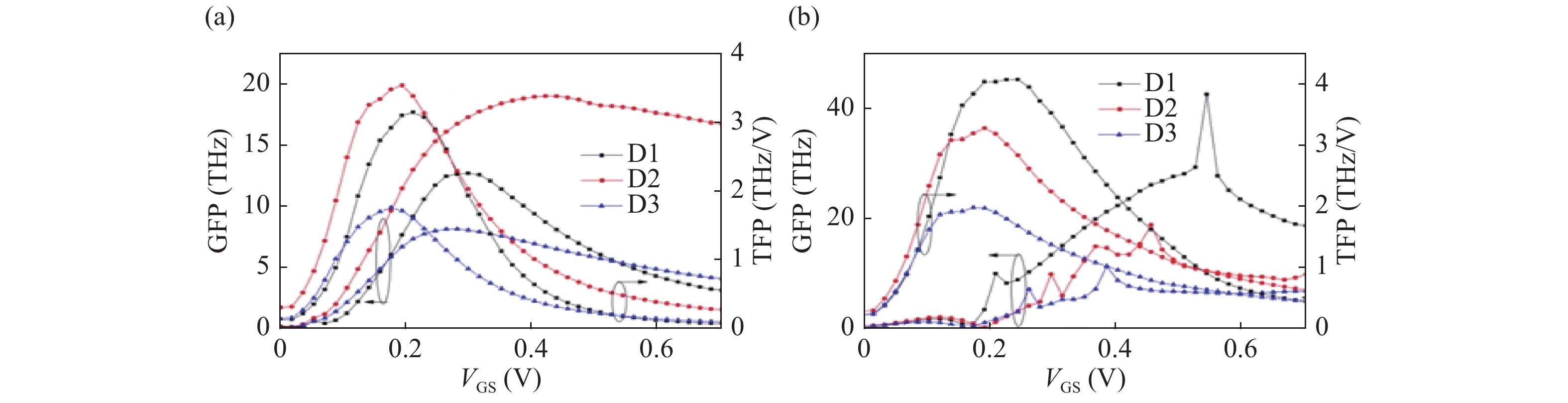
Nowadays FinFET devices have replaced the MOS devices almost in all complex integrated circuits of electronic gadgets like computer peripherals, tablets, and smartphones in portable electronics. The scaling of FinFET is ongoing and the analog/RF performance is most affected by increased SCEs (short channel effects) in sub 22 nm technology nodes. This paper explores the analog/RF performance study and analysis of high performance device-D2 (conventional HfO2 spacer SOI FinFET) and device-D3 (source/drain extended HfO2 spacer SOI FinFET) over the device-D1 (conventional Si3N4 spacer SOI FinFET) at 20 nm technology node through the 3-D (dimensional) simulation process. The major performance parameters like Ion (ON current), Ioff (OFF current), gm (transconductance), gd (output conductance), AV (intrinsic gain), SS (sub-threshold slope), TGF = gm/Id (trans-conductance generation factor), VEA (early voltage), GTFP (gain trans-conductance frequency product), TFP (tans-conductance frequency product), GFP (gain frequency product), and fT (cut-off frequency) are studied for evaluating the analog/RF performance of different flavored SOI FinFET structures. For analog performance evaluation, device-D3 and D2 give better results in terms of gm, ID (drain current) and SS parameters, and for RF performance evaluation device-D1 is better in terms of fT, GTFP, TFP, and GFP parameters both at low and high values of VDS = 0.05 V and VDS = 0.7 V respectively.

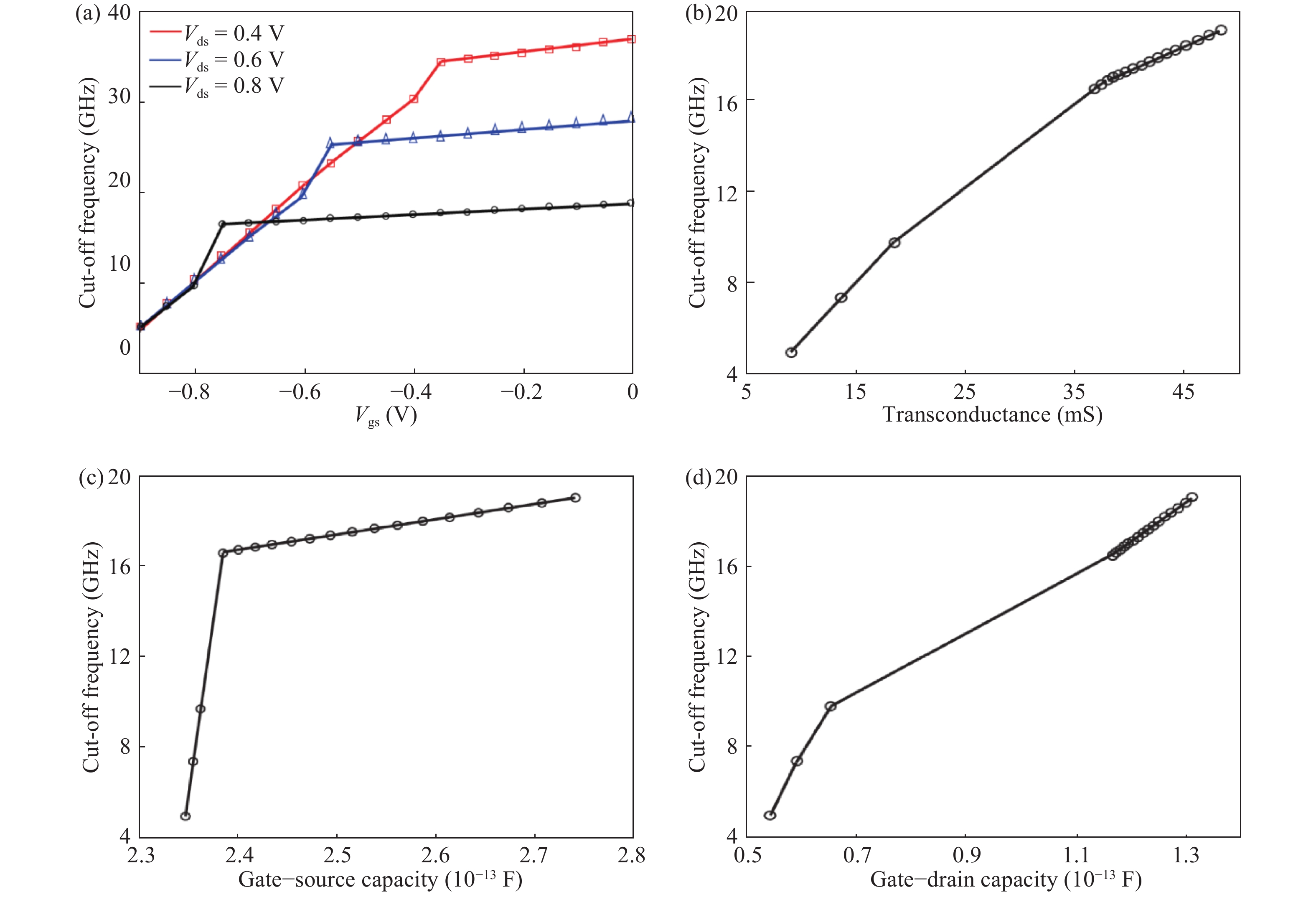
This paper presents a new model to study the static performances of a GaN metal epitaxial-semiconductor field effect transistor (MESFET) based on the metal–semiconductor interface state of the Schottky junction. The I–V performances of MESFET under different channel lengths and different operating systems (pinch-off or not) have been achieved by our model, which strictly depended on the electrical parameters, such as the drain-gate capacity Cgd, the source–gate capacity Cgs, the transconductance, and the conductance. To determine the accuracy of our model, root-mean-square (RMS) errors were calculated. In the experiment, the experimental data agree with our model. Also, the minimum value of the electrical parameter has been calculated to get the maximum cut-off frequency for the GaN MESFET.


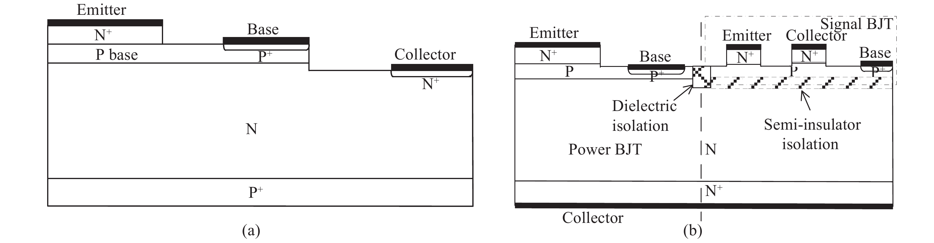
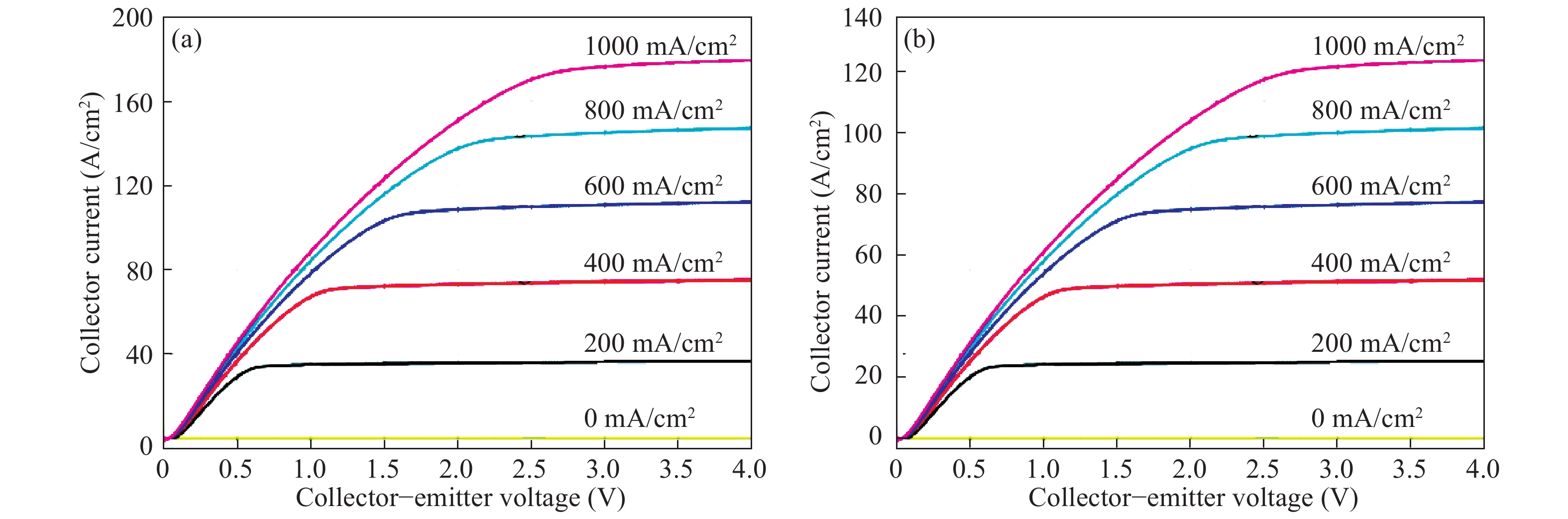
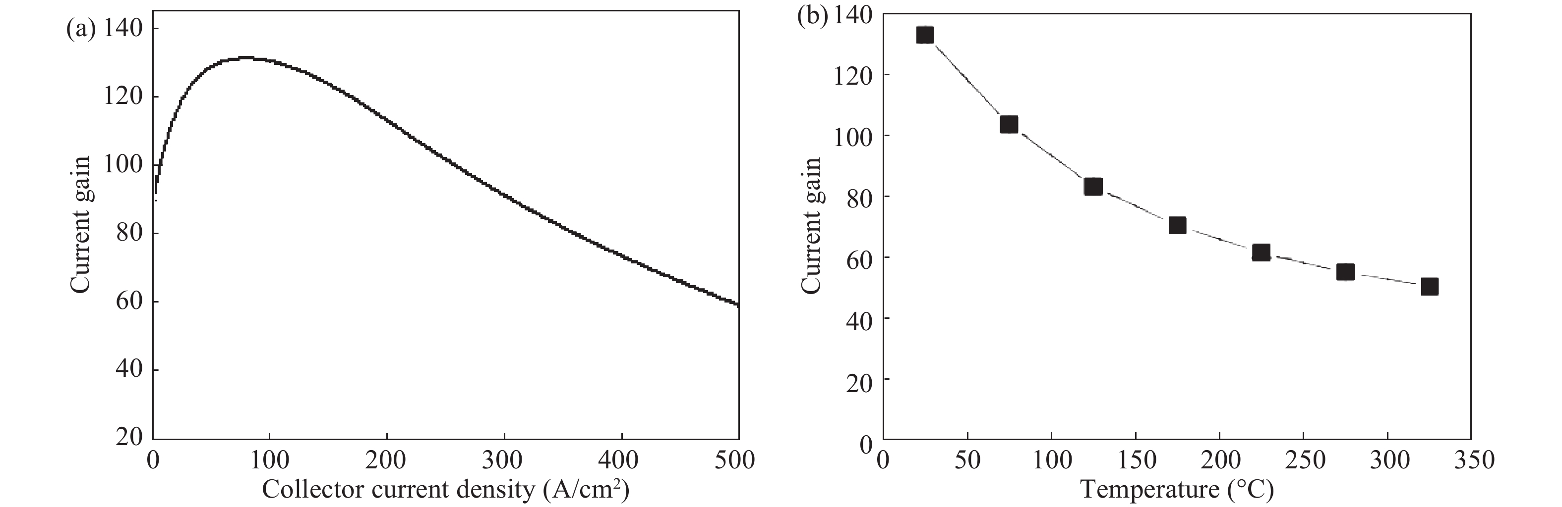
Power integration based on 4H-SiC is a very promising technology for high-frequency and high-temperature power electronics applications. However, the fabrication processes used in Si BiCMOS technology is not applicable in 4H-SiC at present, and few studies on the monolithic power integration of the SiC signal devices and power devices have been reported. In this paper, we propose a novel lateral BJT structure, which is suitable for monolithically integrating with the vertical power BJT on the same epitaxial wafer at the cost of one additional mask. The signal BJT’s static and dynamic characteristics are comprehensively investigated by TCAD simulation. Simulation results show that the common-emitter current gains of the 4H-SiC signal BJT are 133 and 52 at room temperature and 300 °C, respectively. Its implementation in an inverter shows that its switching time is about 200 ns.

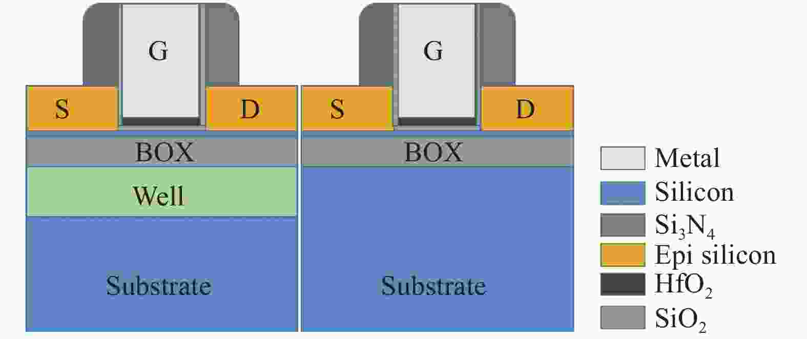
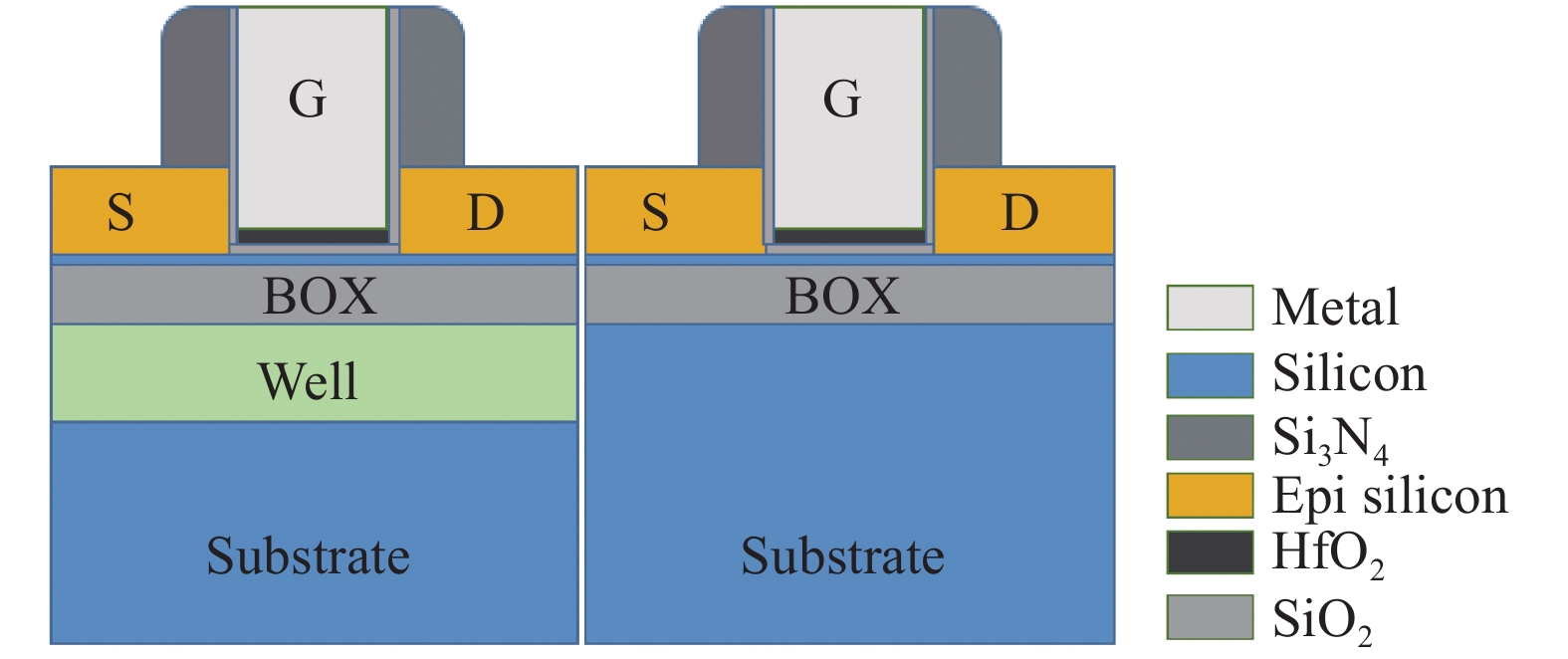
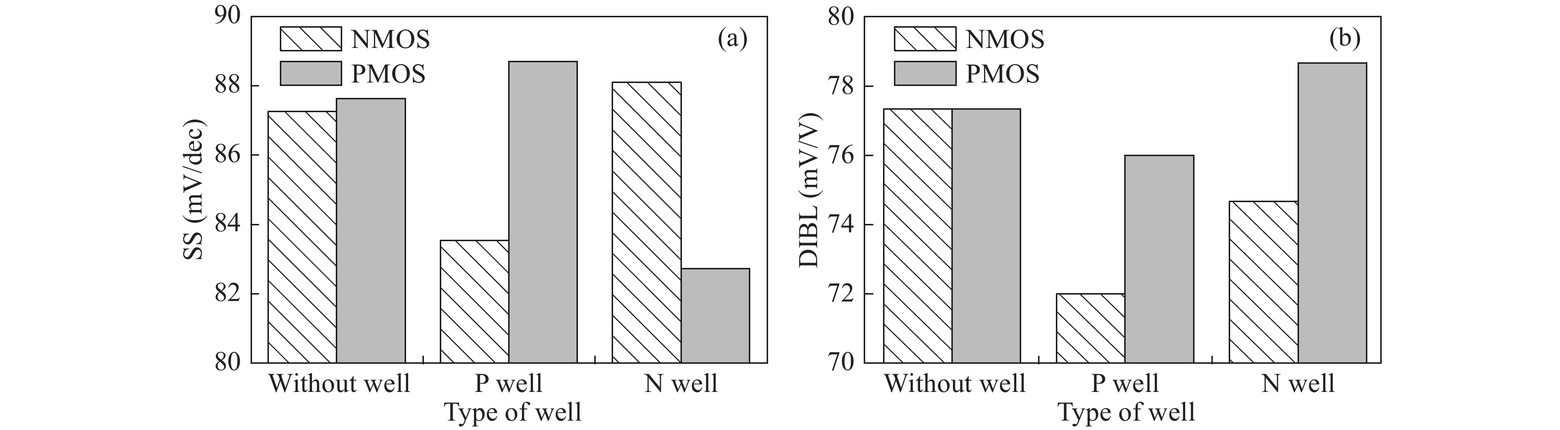
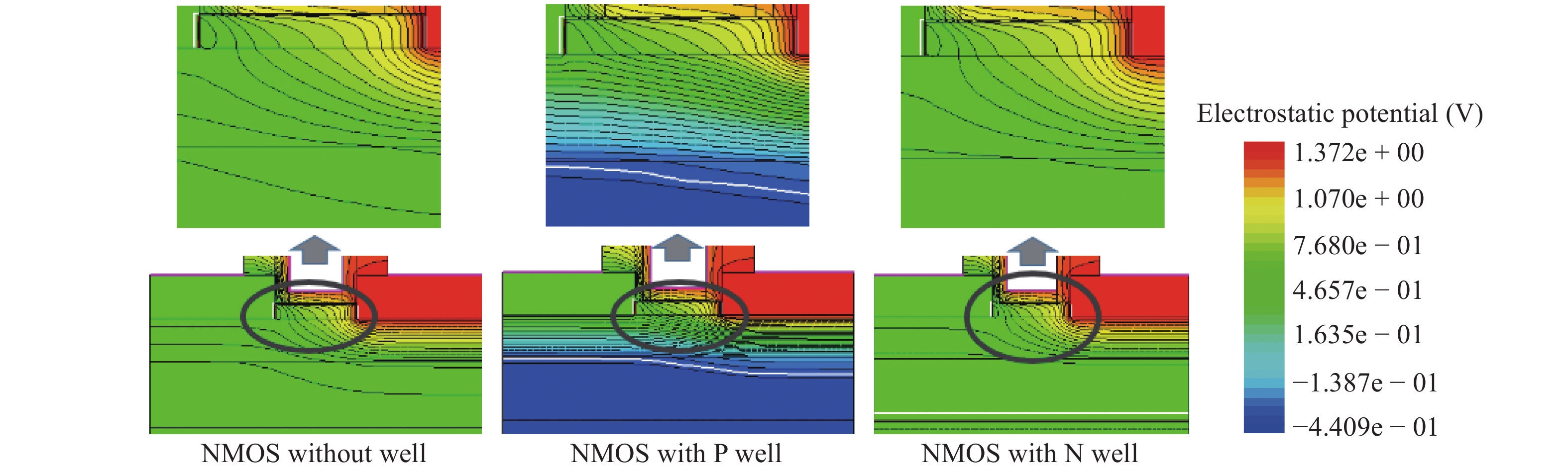
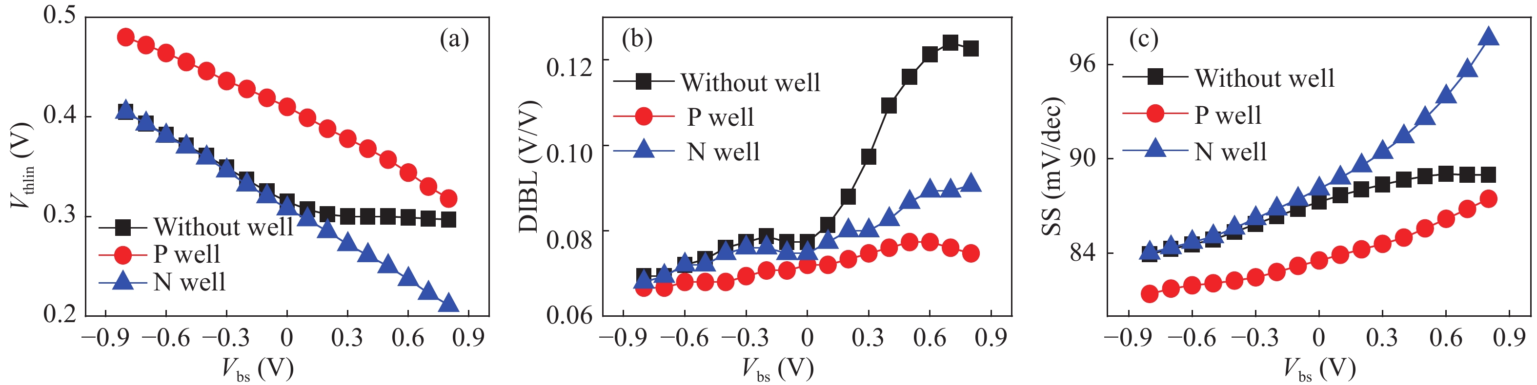
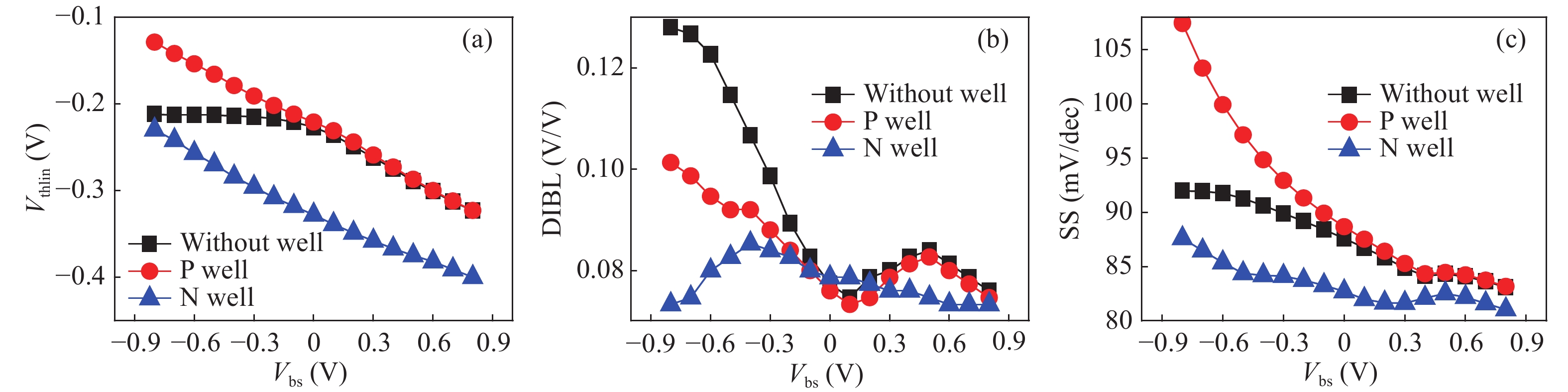
In this work, the impact of well doping and corresponding body bias on UTBB MOSFETs is investigated. The ability of threshold voltage adjustment is evaluated. The results indicate that well doping can change the threshold voltage both of the N and P channel UTBB MOSFETs. The maximum amplitude for a typical 26 nm gate length device is about 100 mV, and these correspond to the cases of devices with an inverse type of high concentration dopant. The body bias adjusts the threshold voltage at a rate of 100–140 mV/V for the UTBB MOSFETs with a well. By optimizing well doping and body biasing, multi-threshold-voltage UTBB MOSFETs can be designed and optimized for lower power application.


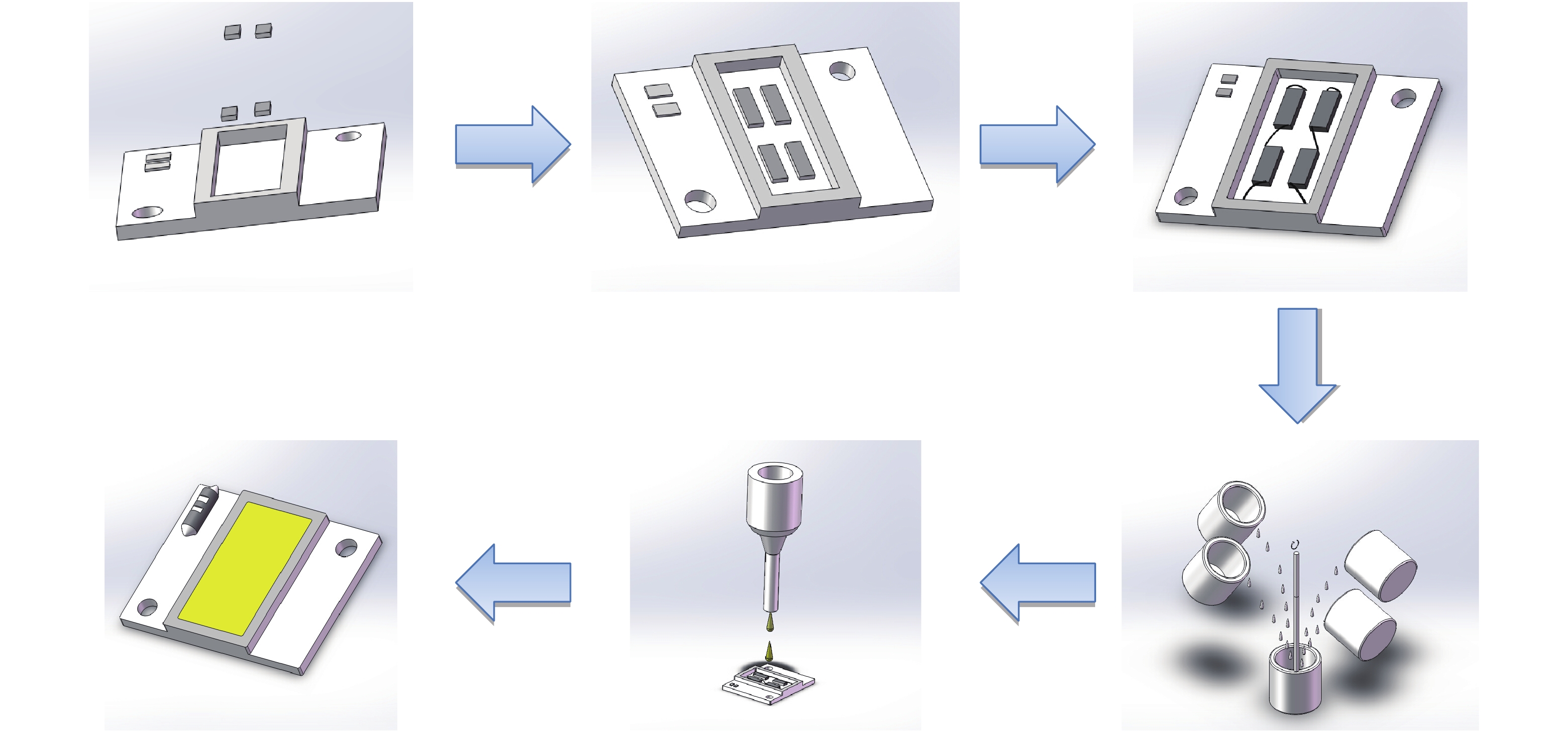
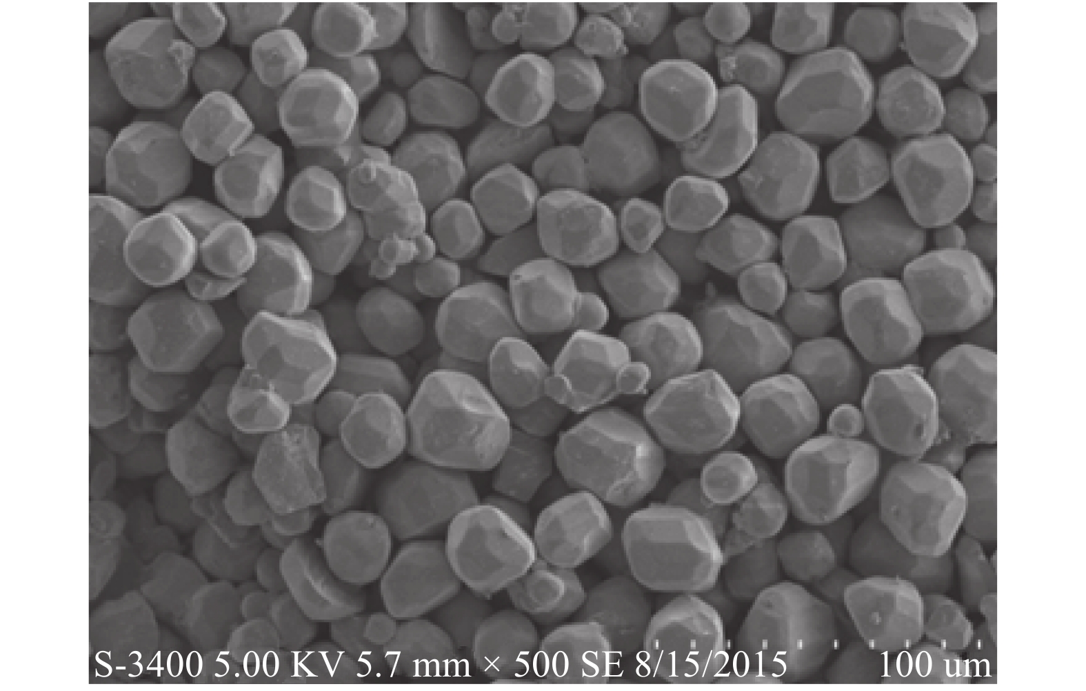
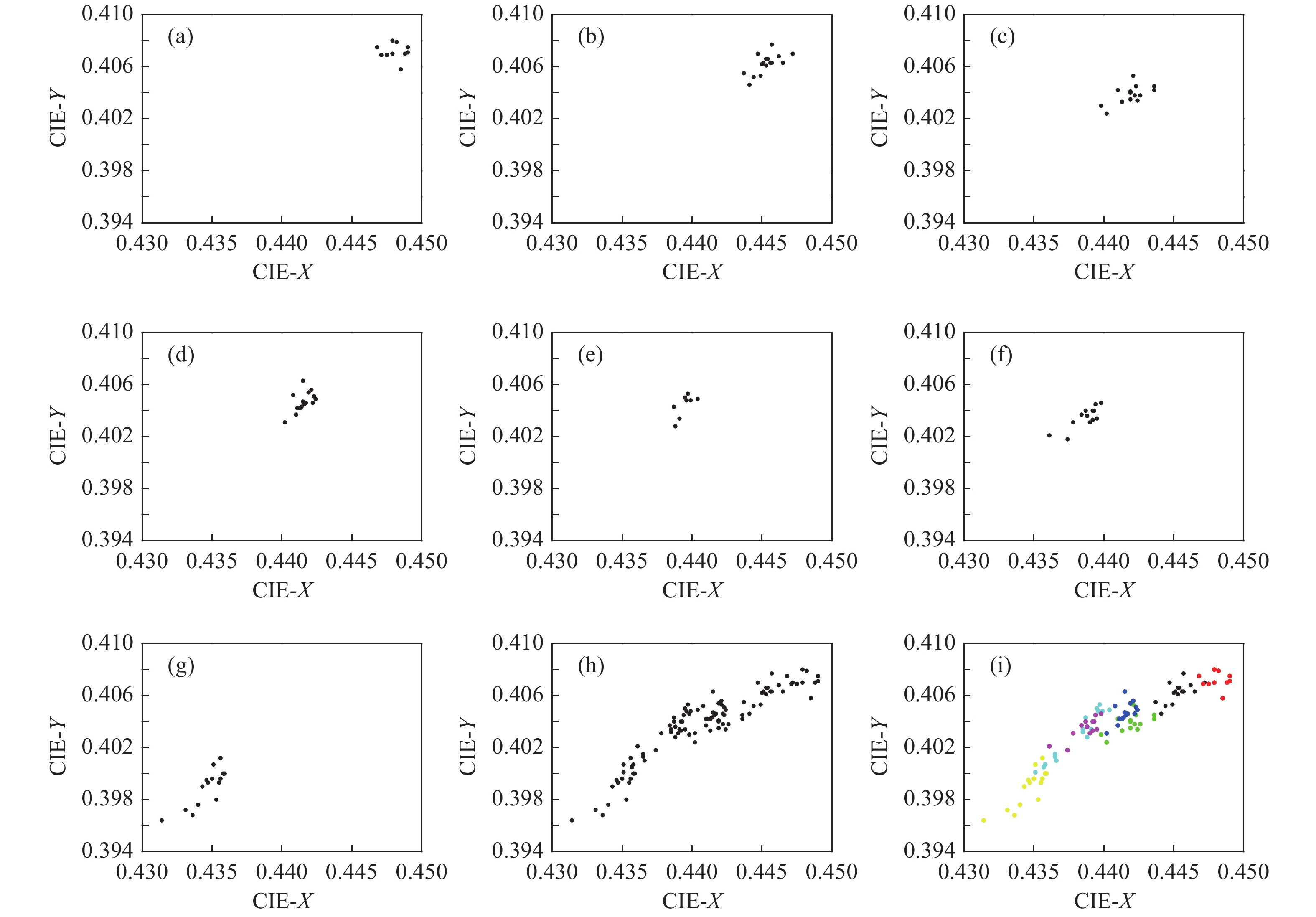
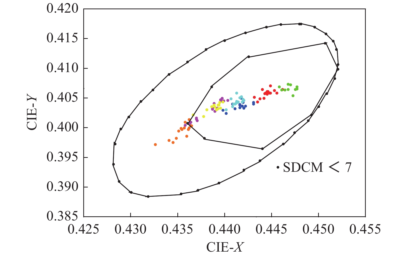
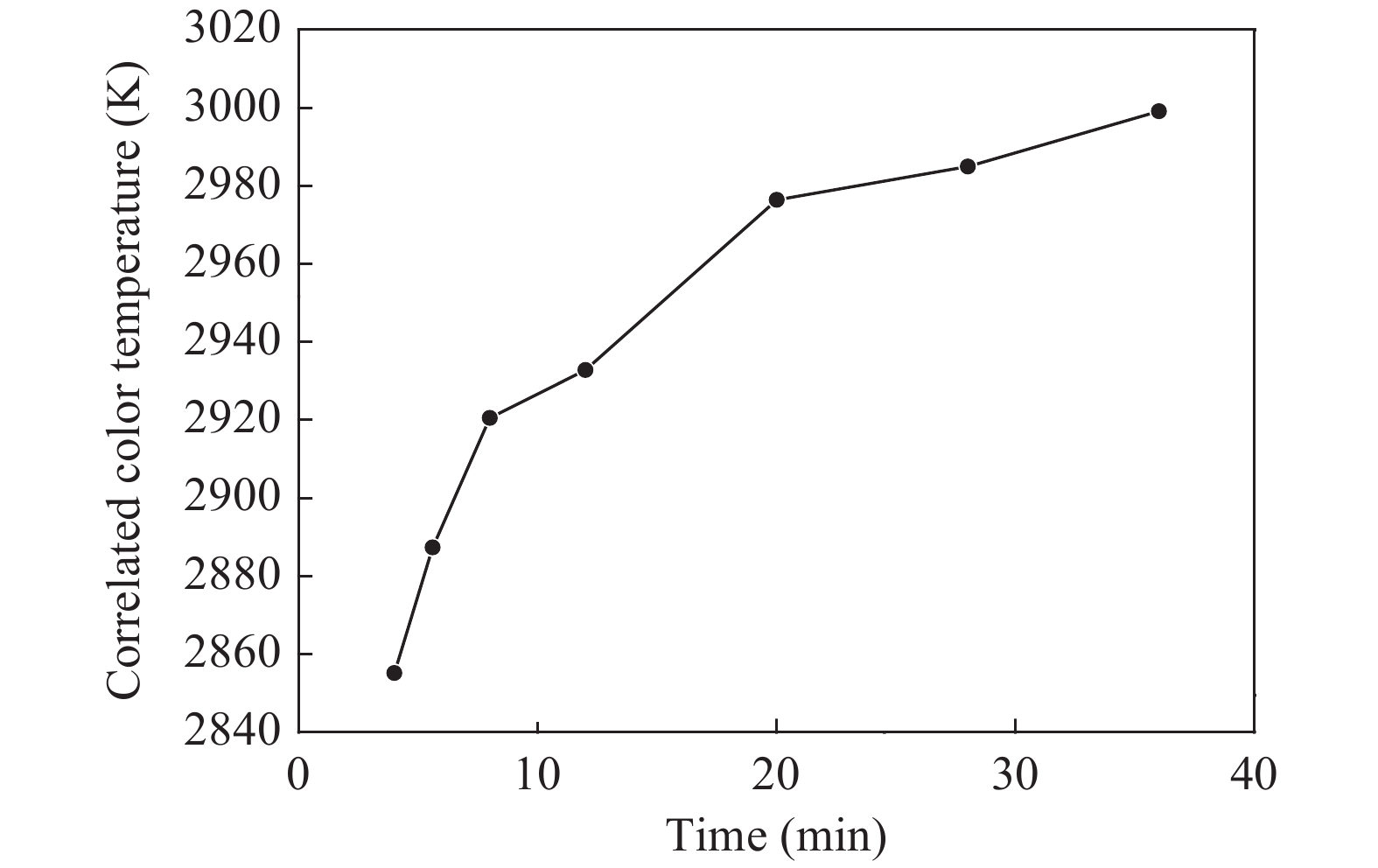
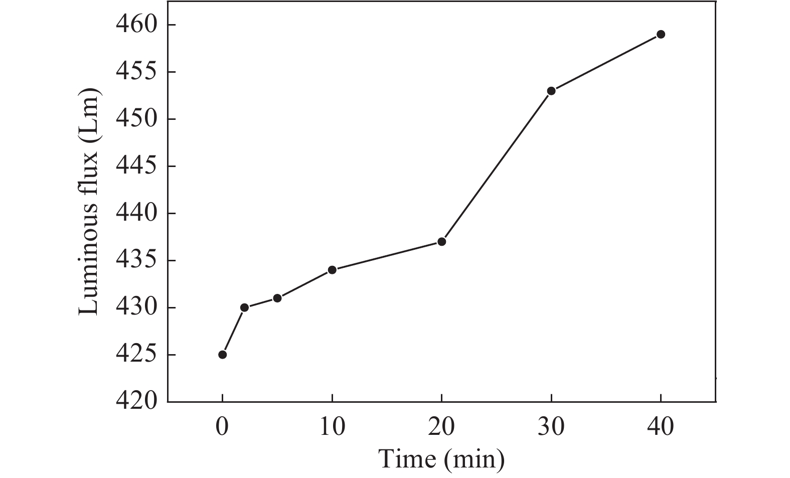
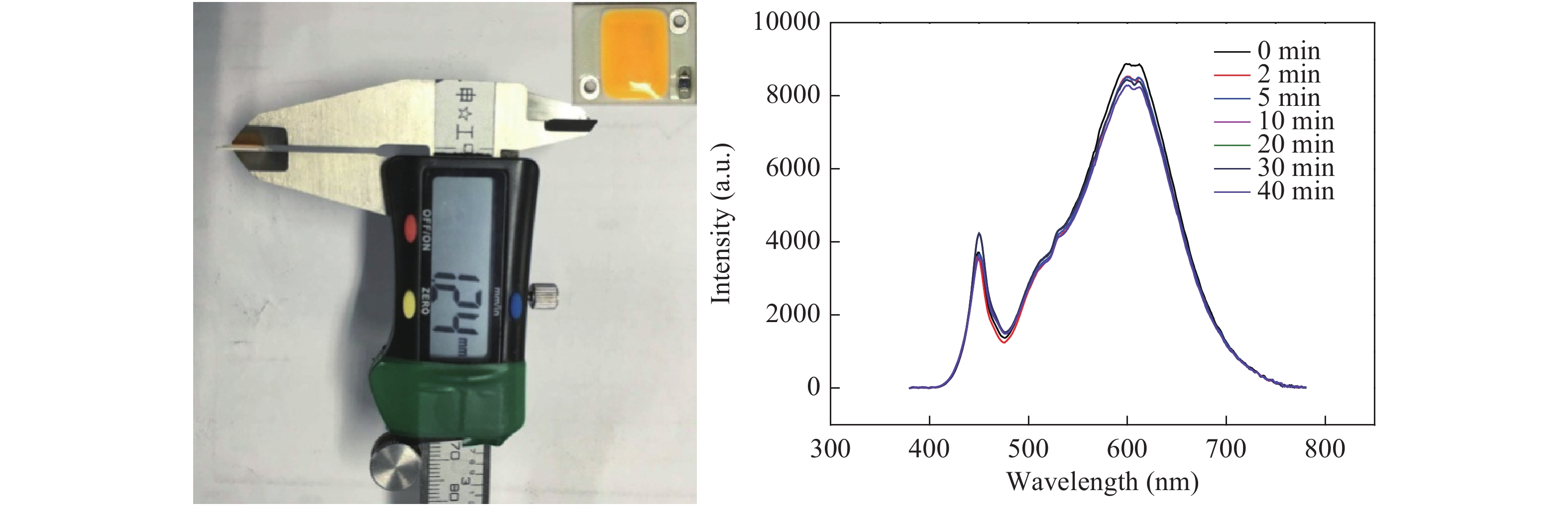
In the process of producing a white light emitting diode, the consistency of the optical coherence and stability of the photochromic properties is a crucial index for measuring the quality of the product. Phosphor sedimentation is a significant factor affecting optical coherence, thus, in this paper, seven sets of control experiments were set up with the phenomenon of the phosphor precipitation at time intervals 0, 2, 5, 10, 20, 30, and 40 min. The color coordination concentration and optical properties were also tested. The results indicate that phosphor sedimentation occurs between 0 and 20 min, during which the color coordinate placement is concentrated, the central coordinates are (x = 0.4432 ± 0.004, y = 0.4052 ± 0.002); the quality was verified because the supply demand chain management (SDCM) was no greater than 7. Later, between 30 and 40 min, the central coordinates are (x = 0.4366 ± 0.003, y = 0.4012 ± 0.003), which had an SDCM value higher than 7, and had a more discrete color placement; it does not meet the requirements of the national standard GBT24823-2016 general lighting LED module performance.
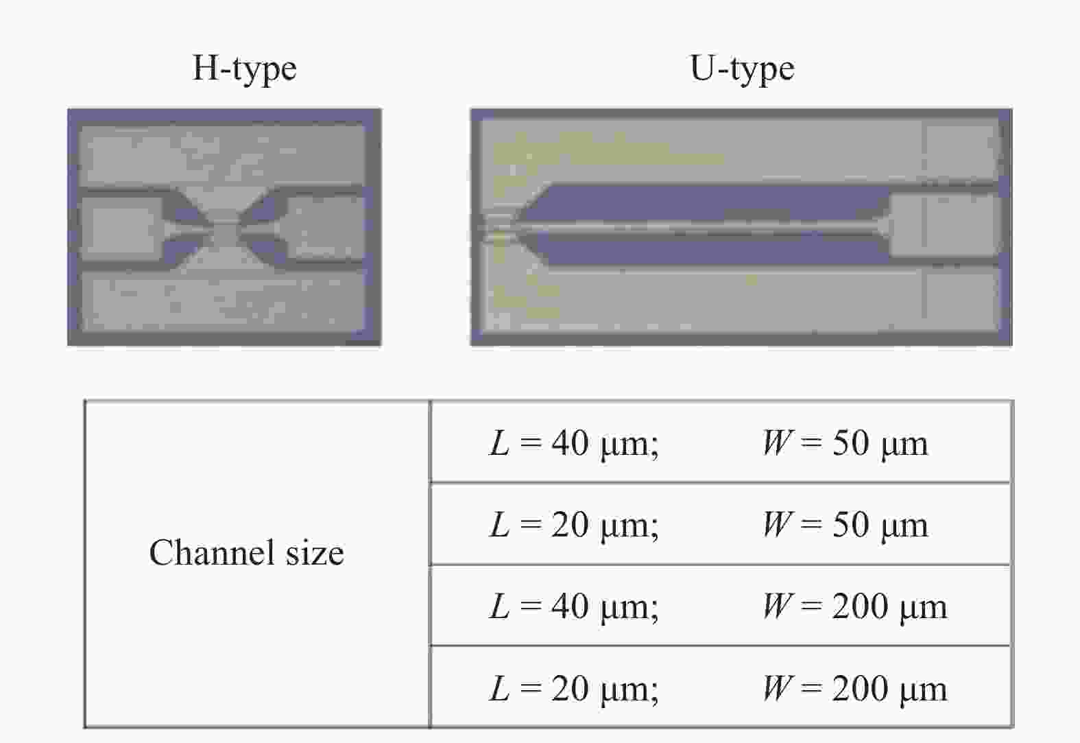
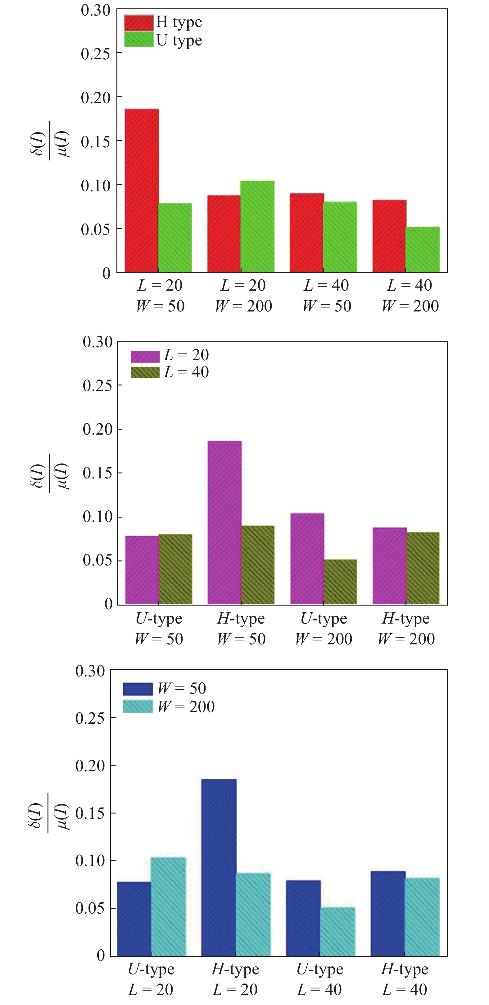
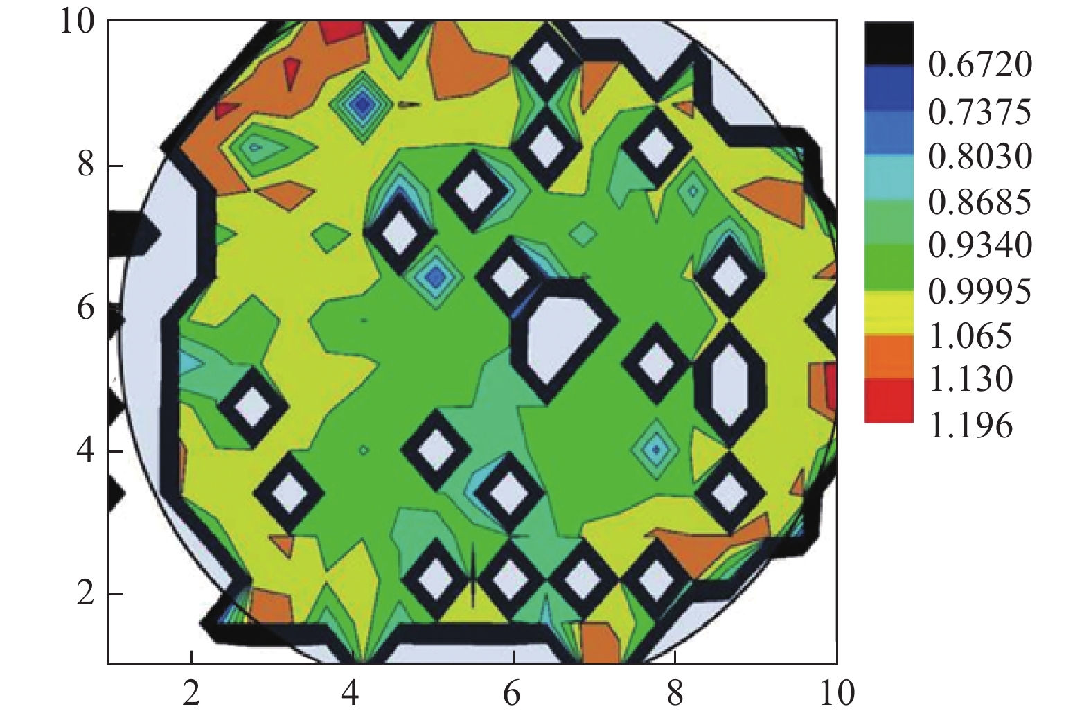
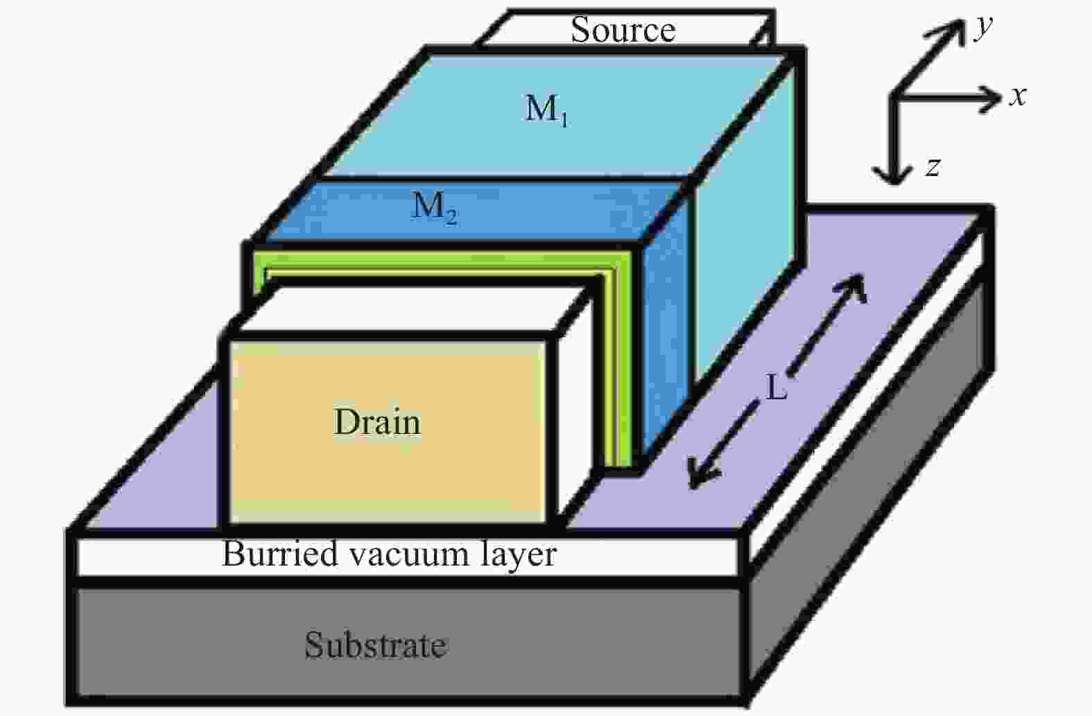
High electron mobility transistors (HEMT) have the potential to be used as high-sensitivity and real-time biosensors. HEMT biosensors have great market prospects. For the application of HEMT biosensors, the electric properties consistency of the inter-chip performance have an important influence on the stability and repeatability of the detection. In this research, we fabricated GaAs/AlGaAs HEMT biosensors of different epitaxial structures and device structures to study the electric properties consistency. We study the relationship between channel size and consistency. We investigated the distribution of device current with location on 2 inch GaAs wafer. Based on the studies, the optimal device of a GaAs HEMT biosensor is an A-type epitaxial structure, and a U-type device structure, L = 40 μm, W = 200 μm.
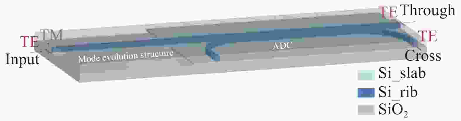
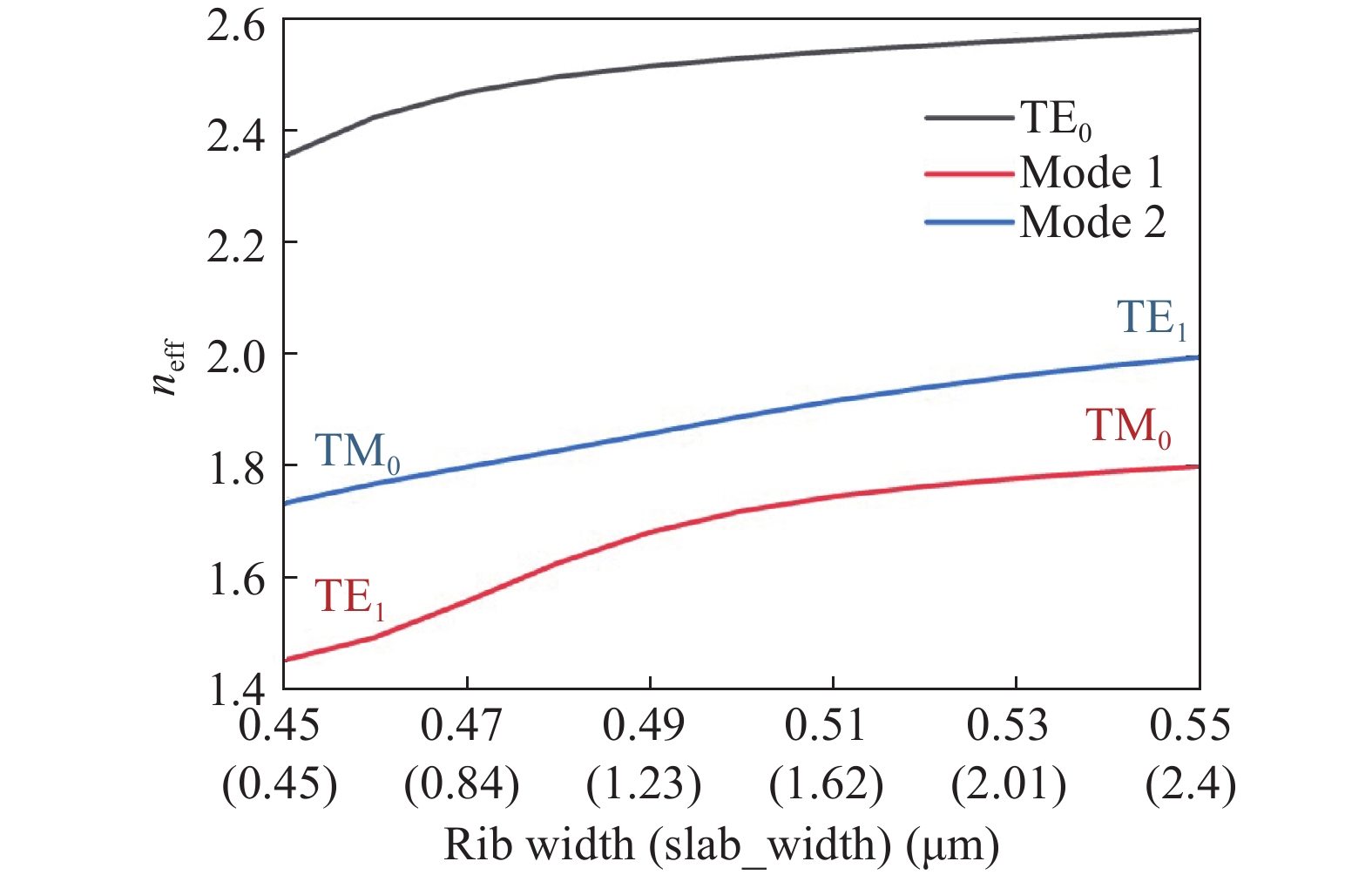
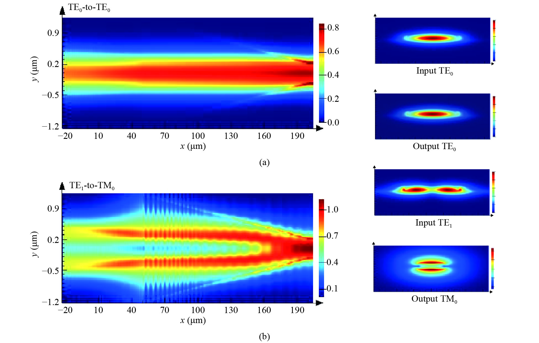
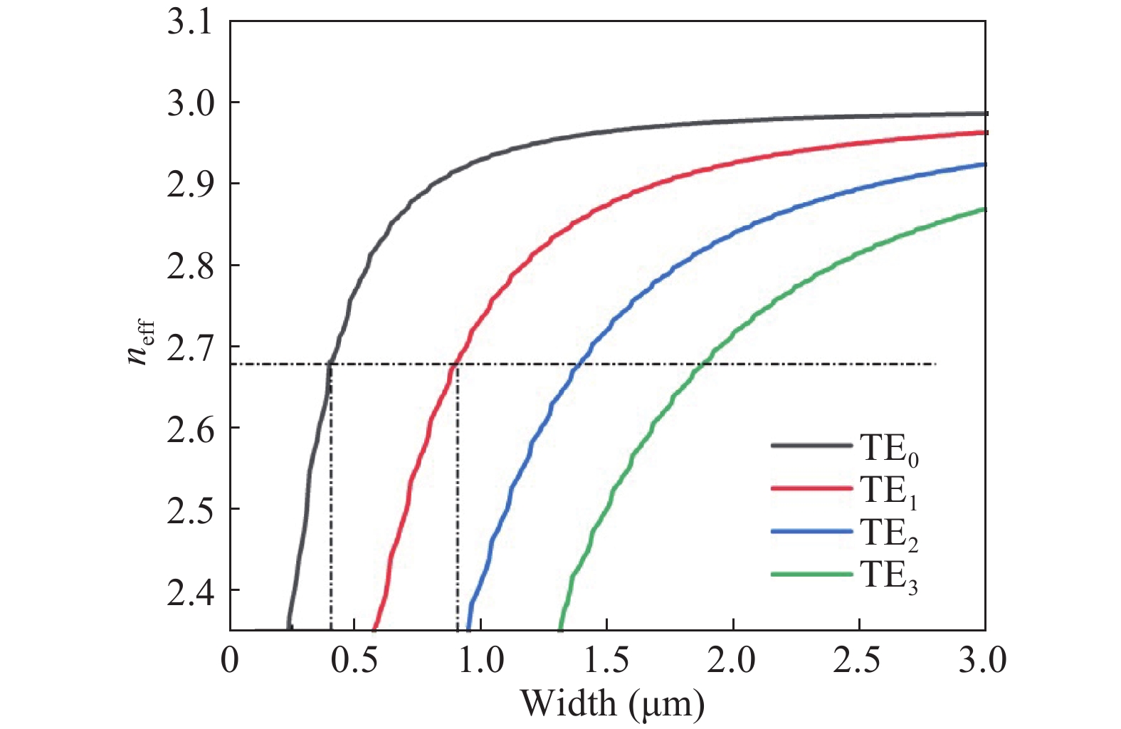
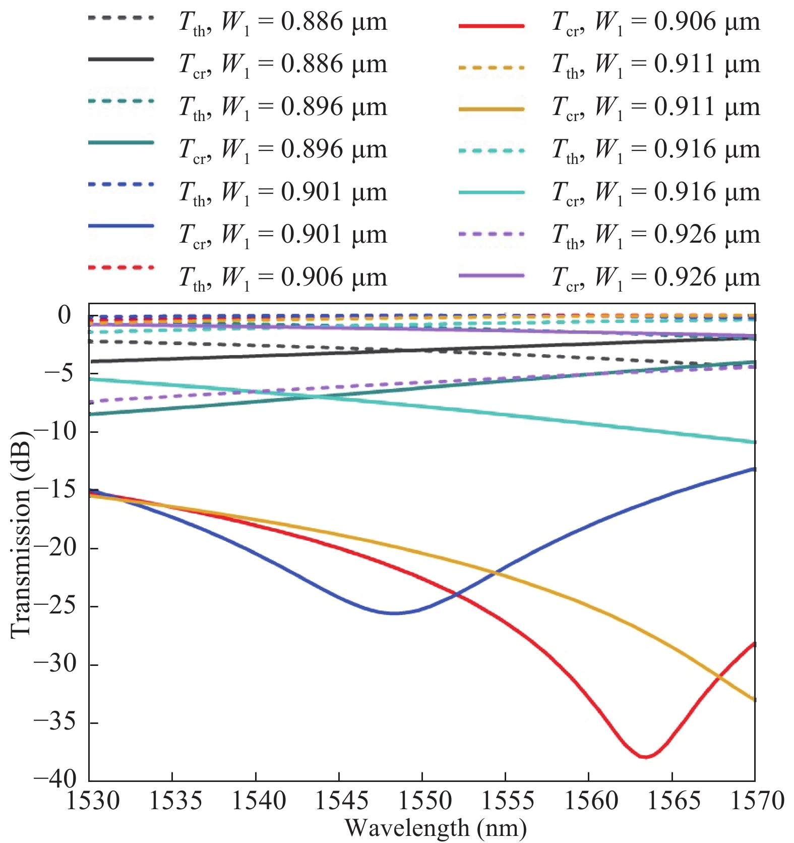
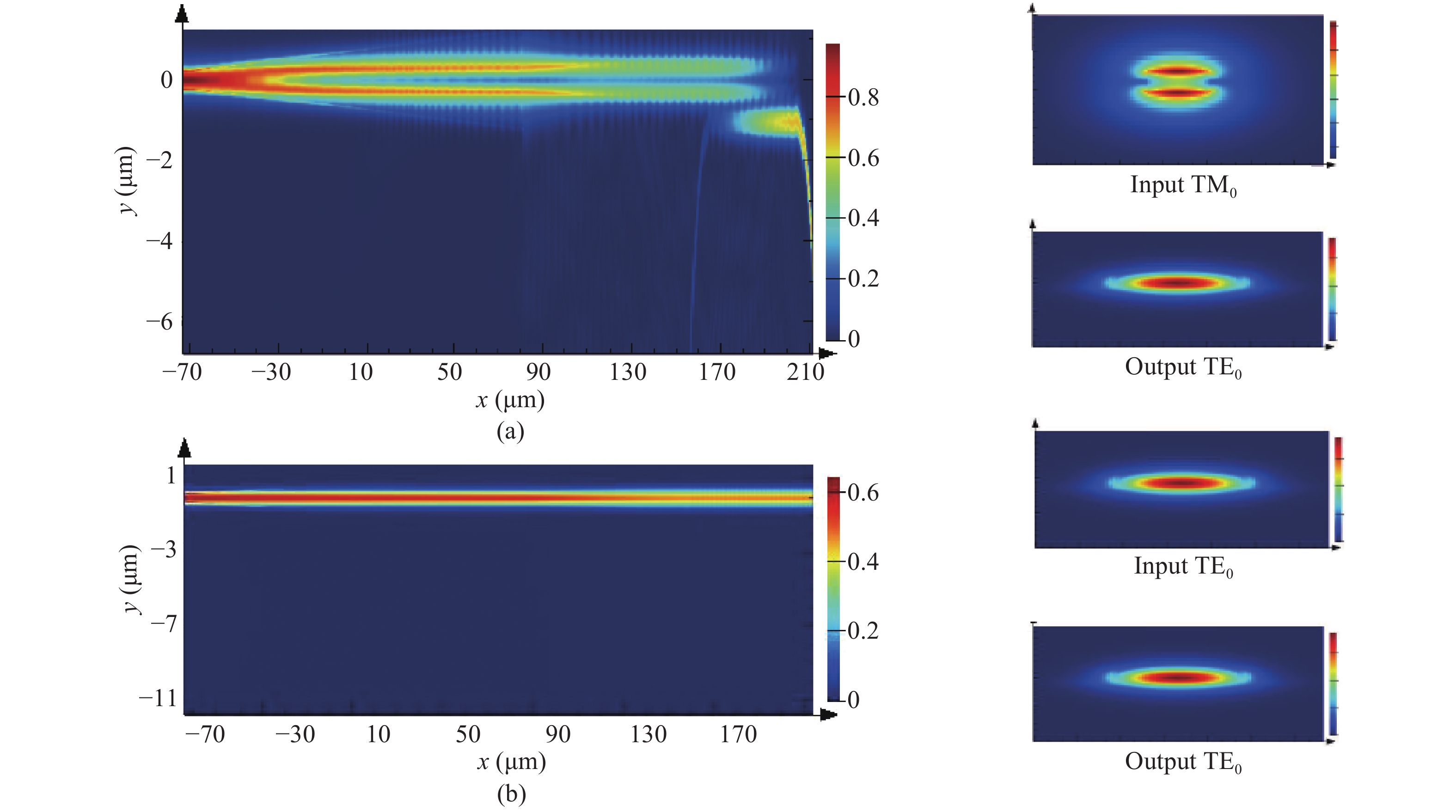
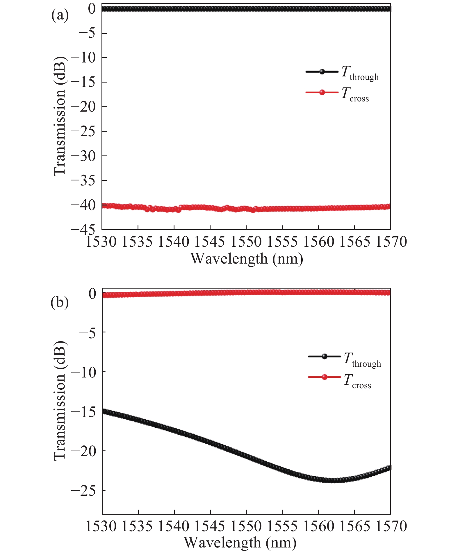
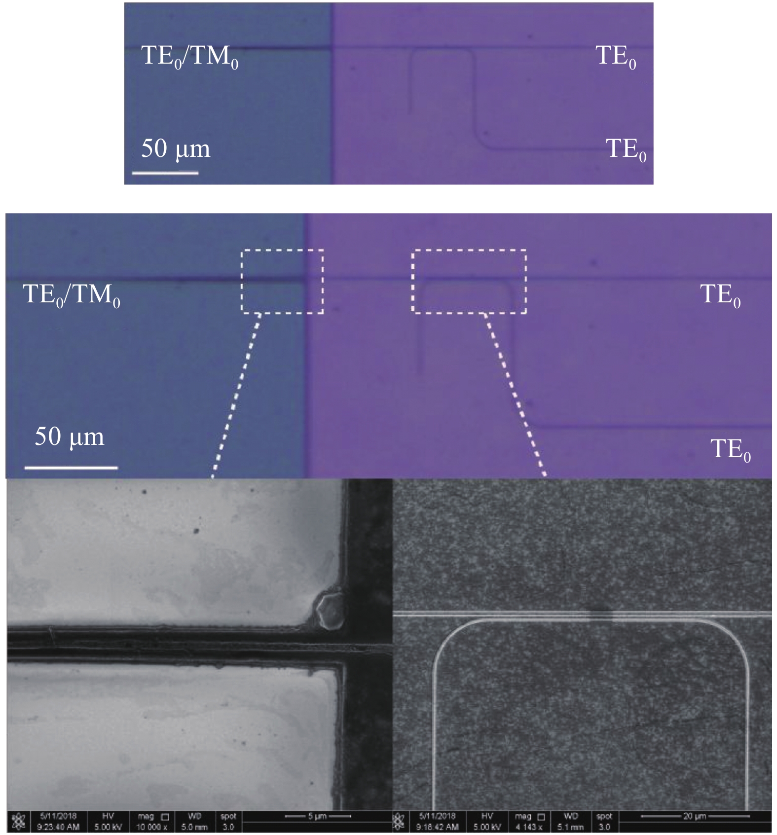
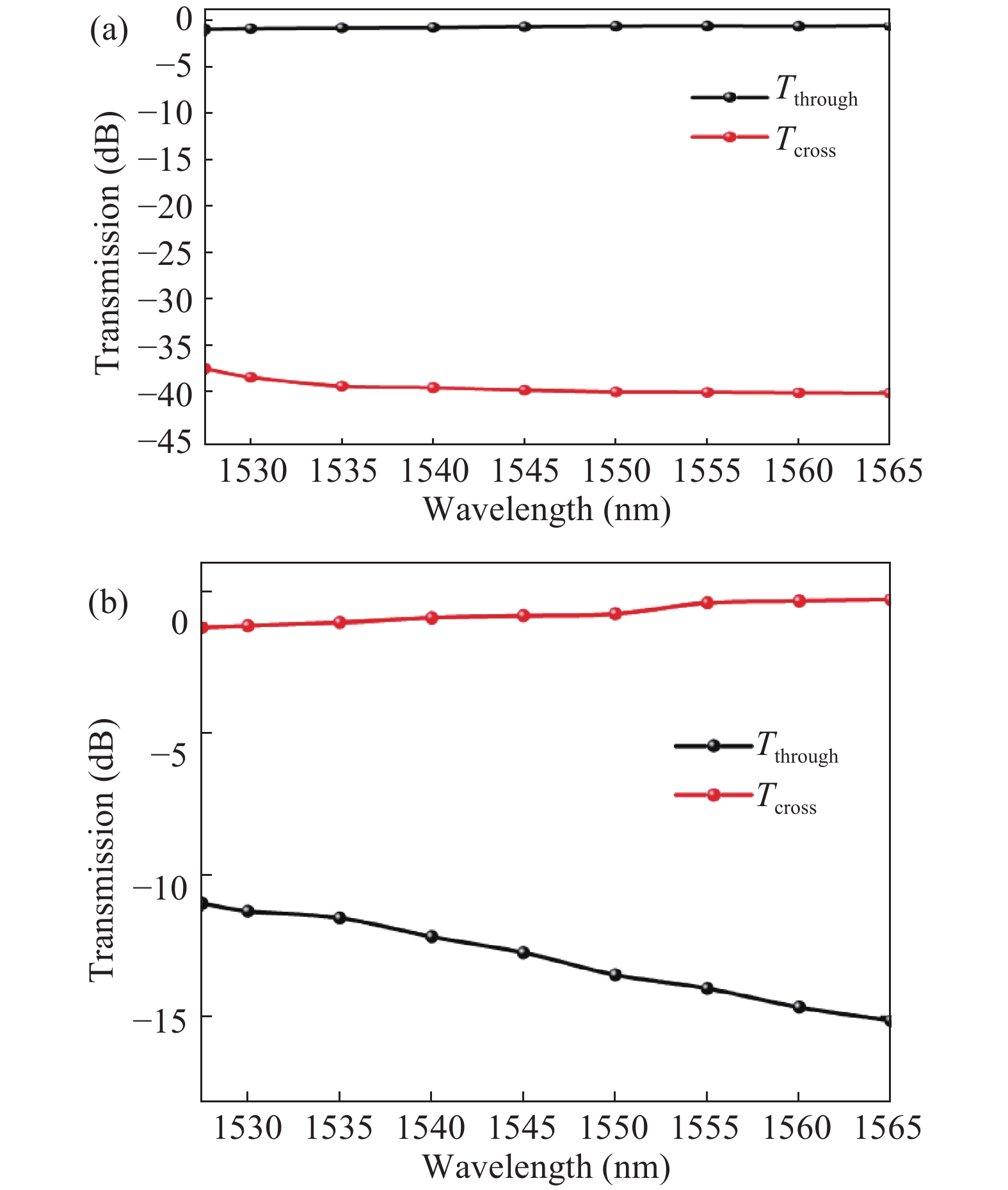
A C-band polarization rotator-splitter based on a mode-evolution structure and an asymmetric directional coupler is proposed. The mode-evolution structure is designed in a bi-level taper through which the TM0 mode can evolve into the TE1 mode. Then the TE1 mode is coupled to the TE0 mode at the cross port using the asymmetric directional coupler. The input TE0 mode propagates along the waveguide without mode conversion and output at the through port. From the experimental results, the extinction ratio is lower than 30 dB and the excess loss is less than 1 dB for input TE0 mode at the whole C-band. For input TM0 mode, the ER and the EL are, respectively, lower than −10 and 1.5 dB.


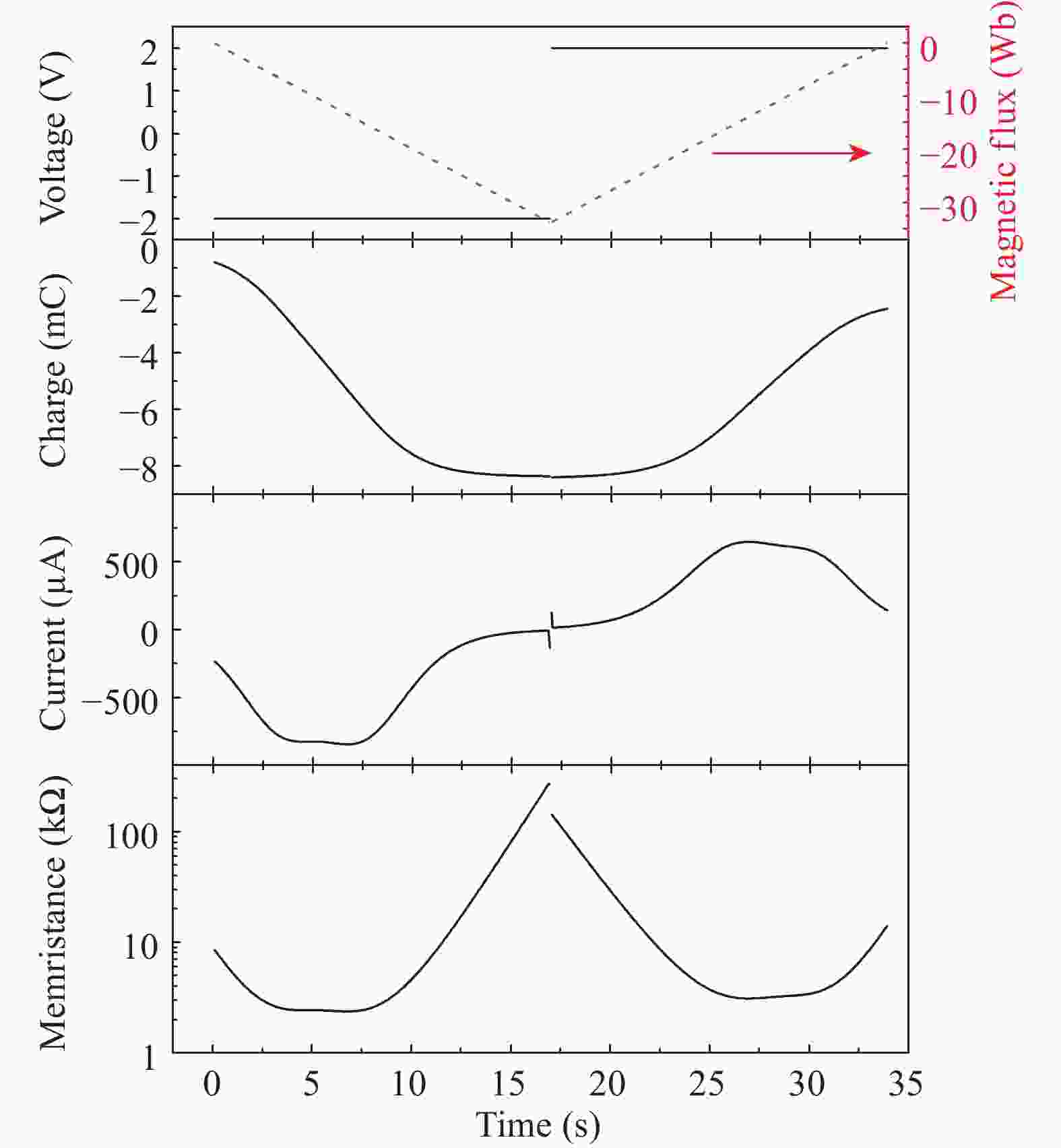
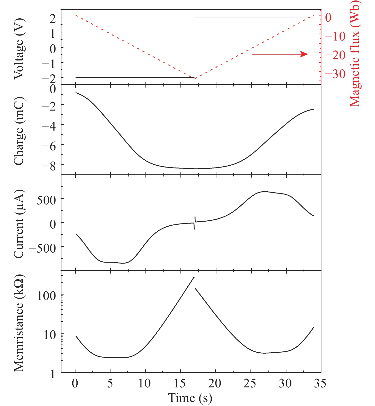
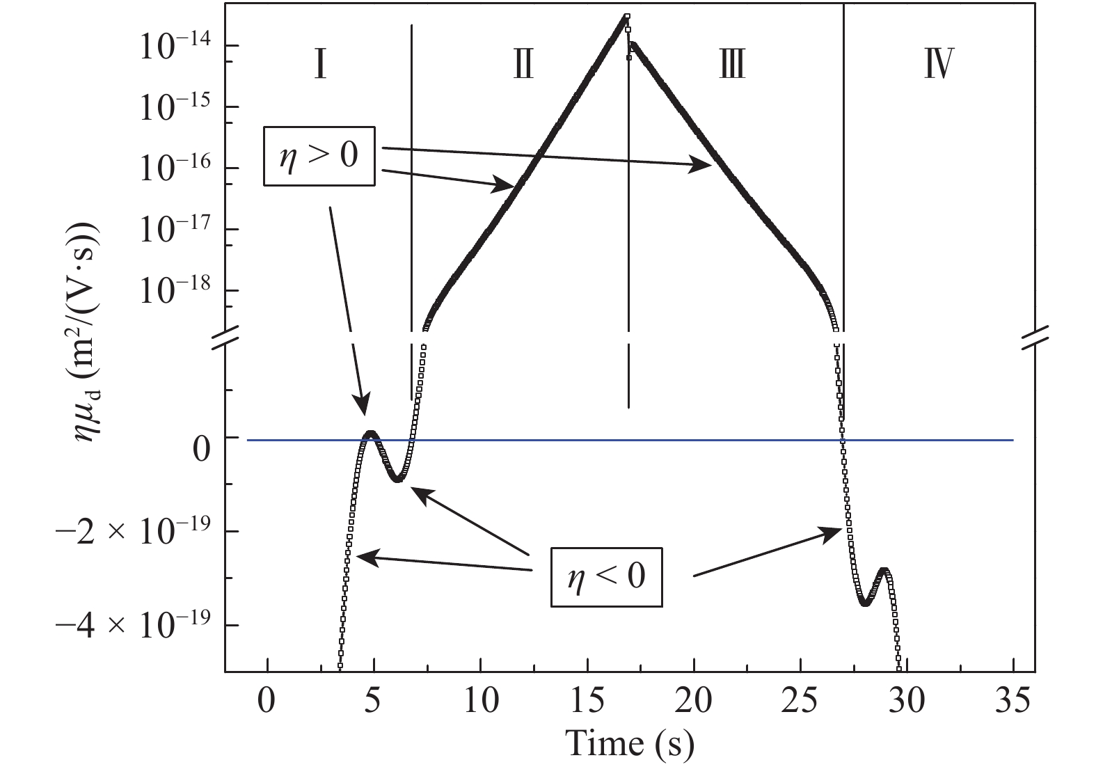
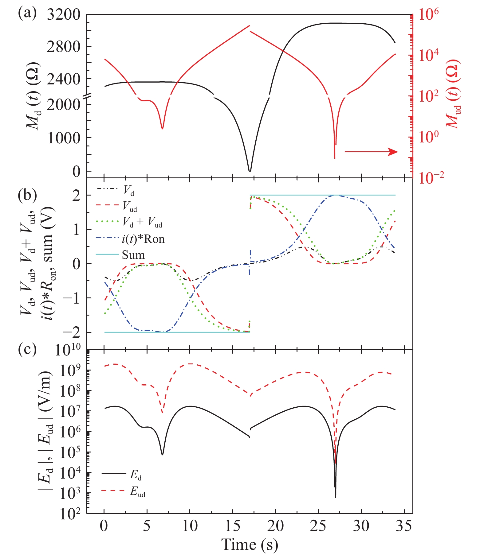
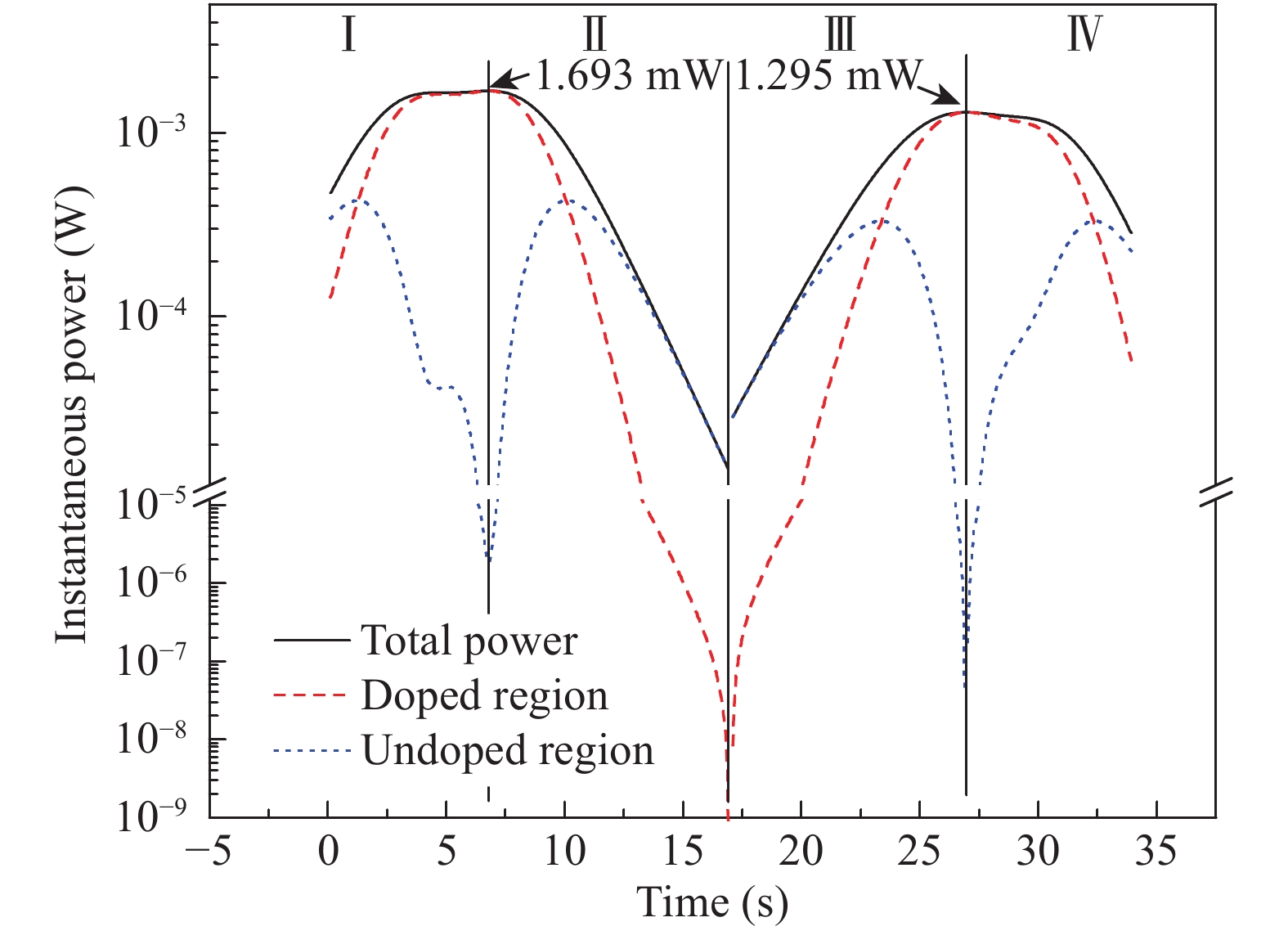
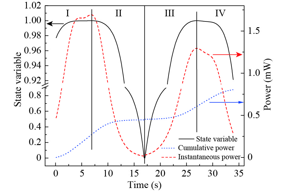
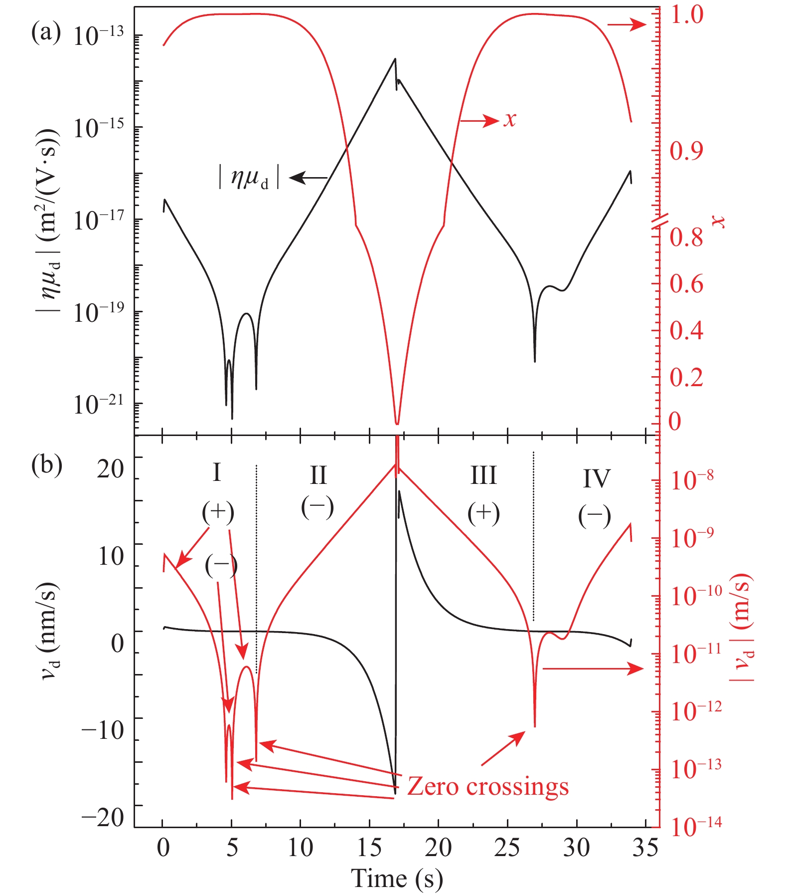
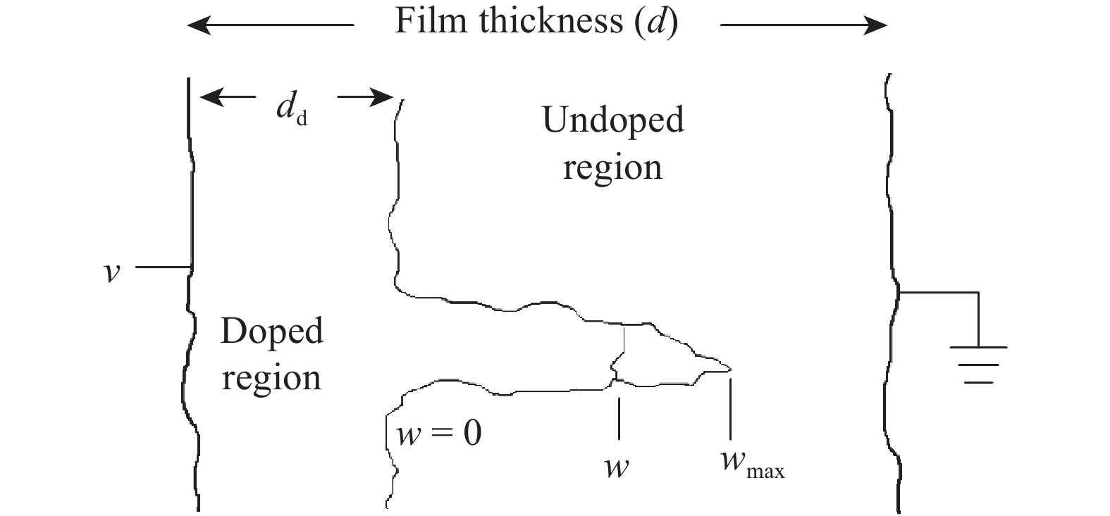
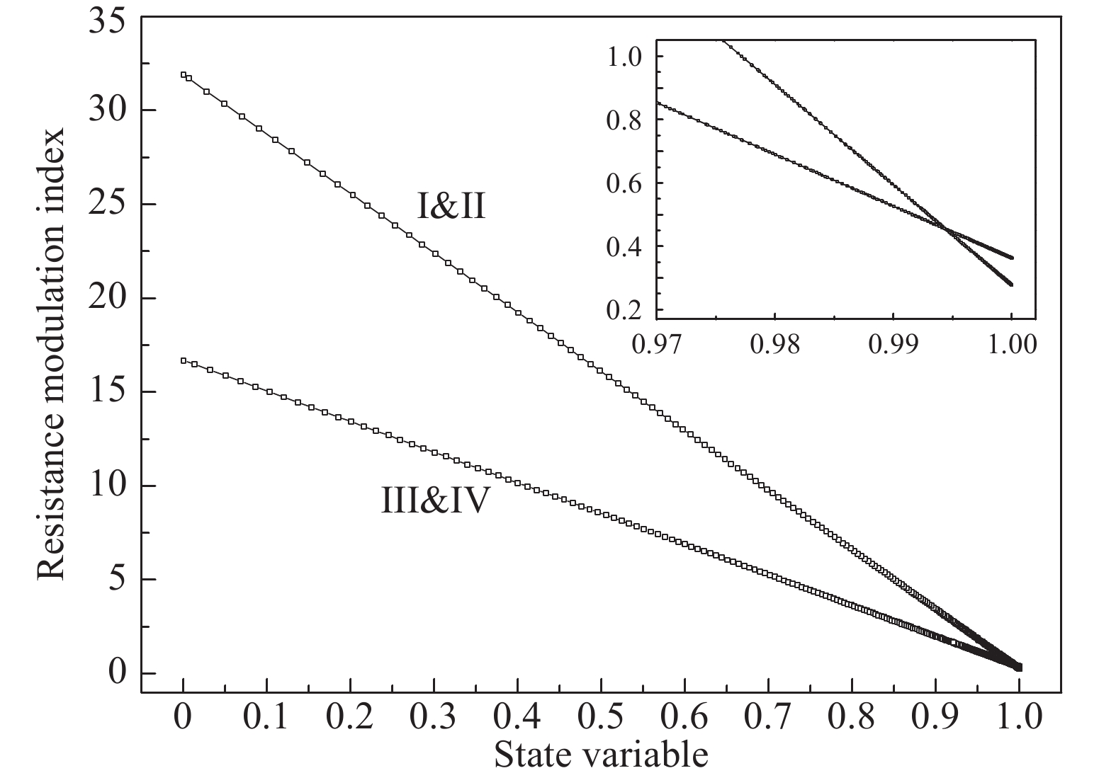
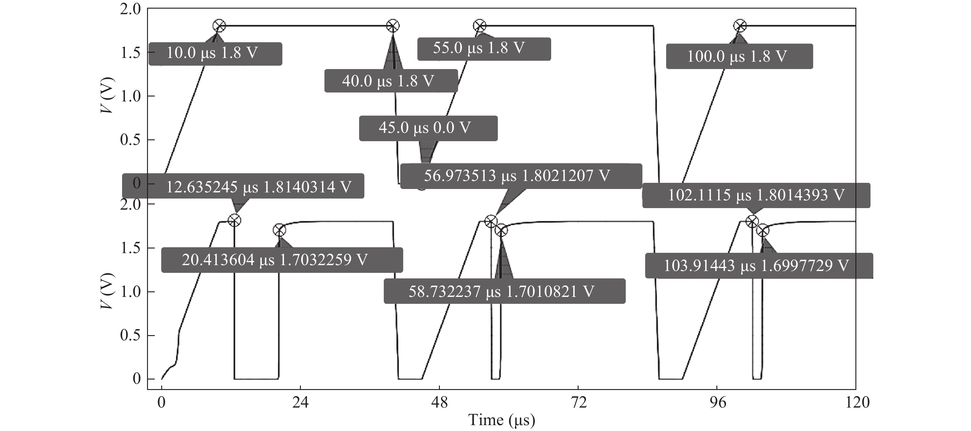
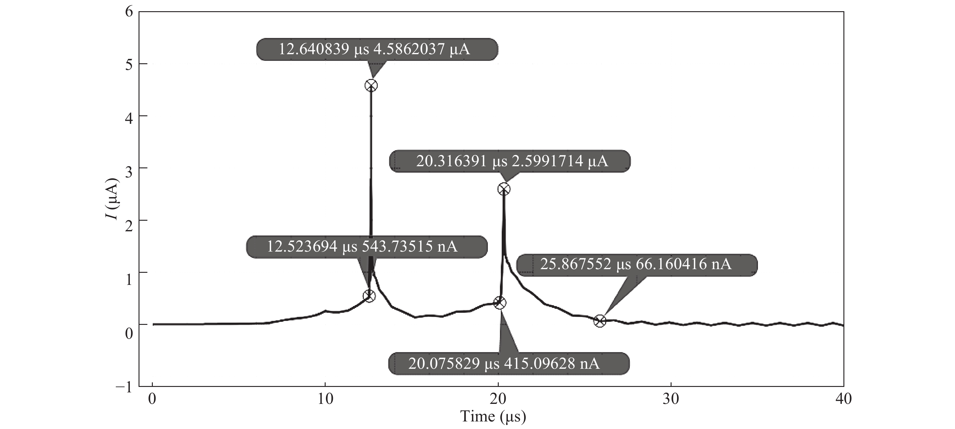
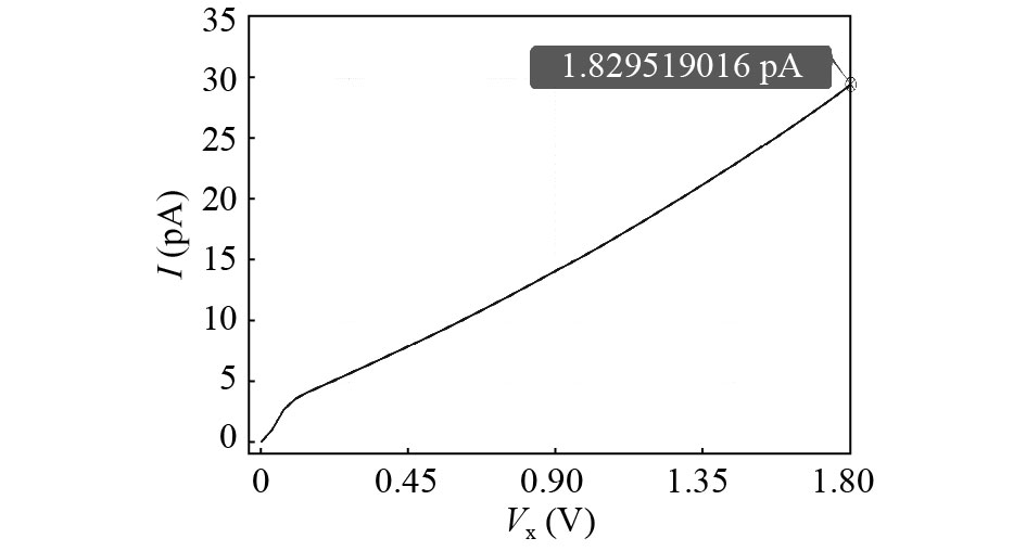
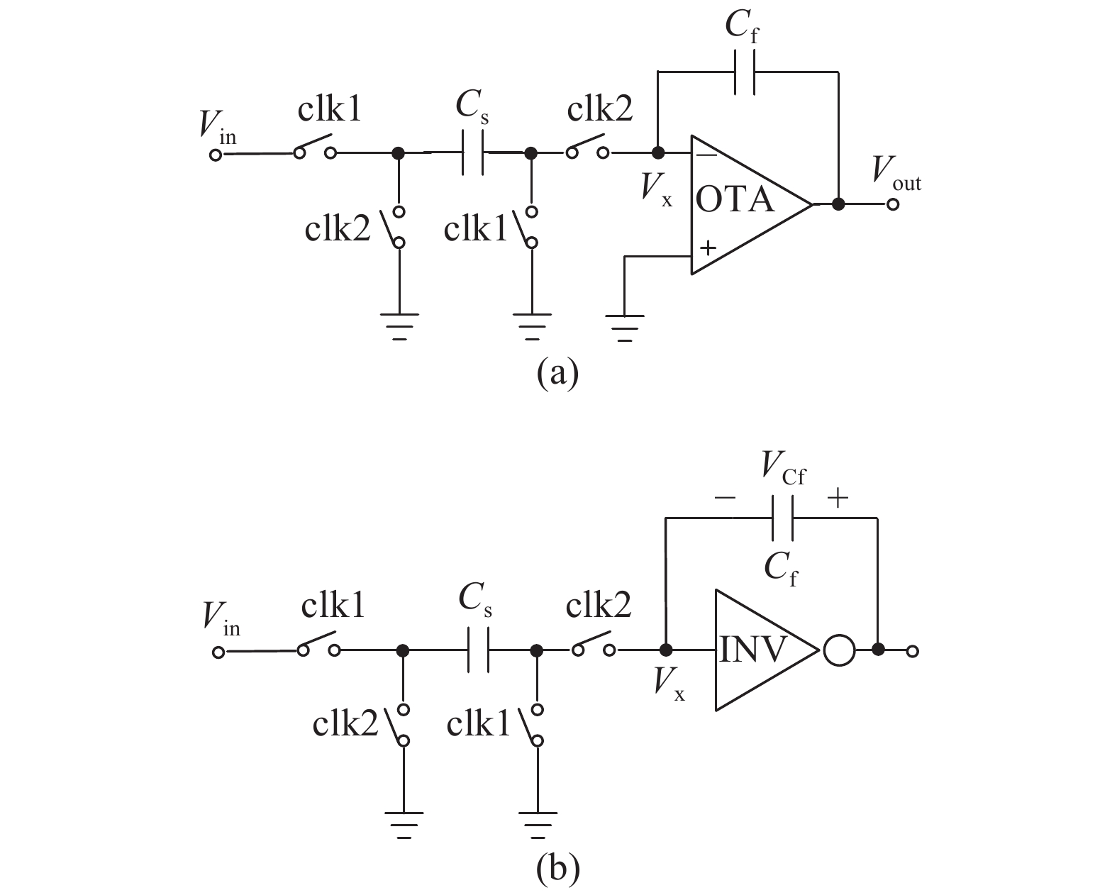
Diverse models have been proposed for explaining the electrical performance of memristive devices. In principle, the behavior of internal variables associated to each one could be extracted from experimental results. In a former work, thermally grown TiOx memristive structures were built and characterized to obtain the constitutive relationship (magnetic flux versus charge). The aim of this work is to continue that analysis by determining the microscopic parameters within the frame of a simple model. We use the already obtained memristance dependence of time and the basic expressions from the non-linear model proposed by Strukov et al. to compute the state-variable, the mobility of the doping species, the speed of the boundary between the doped and the undoped regions, the voltages and the electric fields on the distinct regions. The power dissipation and its time evolution are also presented. Moreover, a quite different window function from those formerly proposed, which was estimated from experimental data, is also determined. This information provides a straightforward picture of the ionic transport during one cycle of a square voltage waveform within the framework of this simple model. Finally, a quality factor is proposed as the key parameter for actual memristors viewed under the same model.

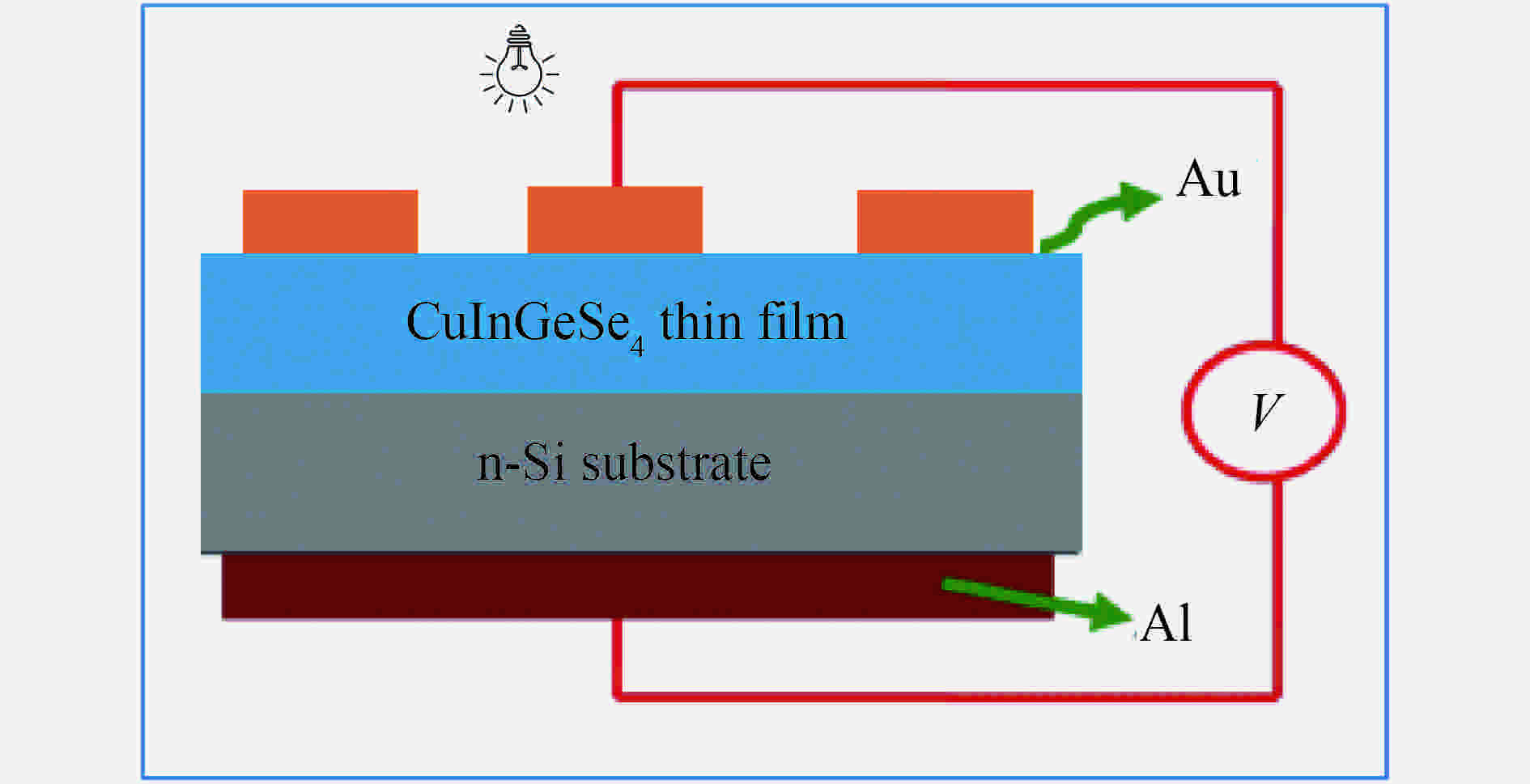
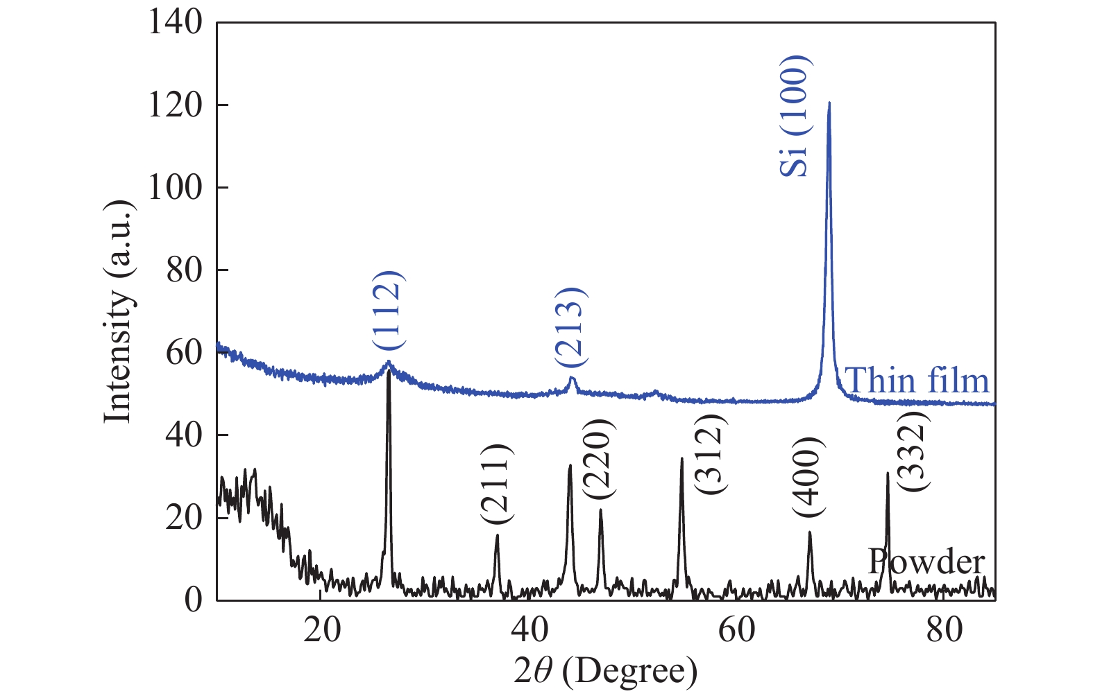
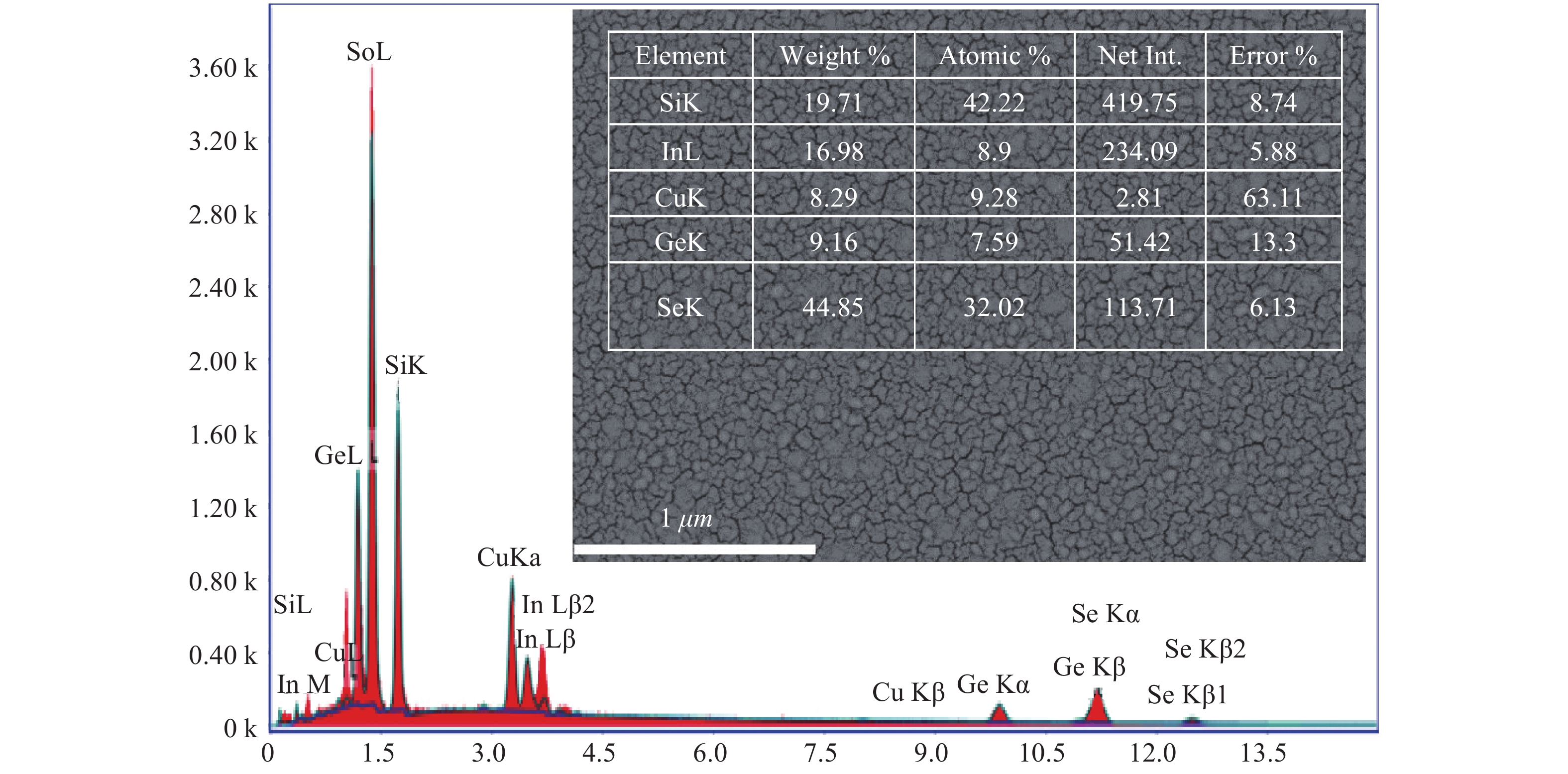
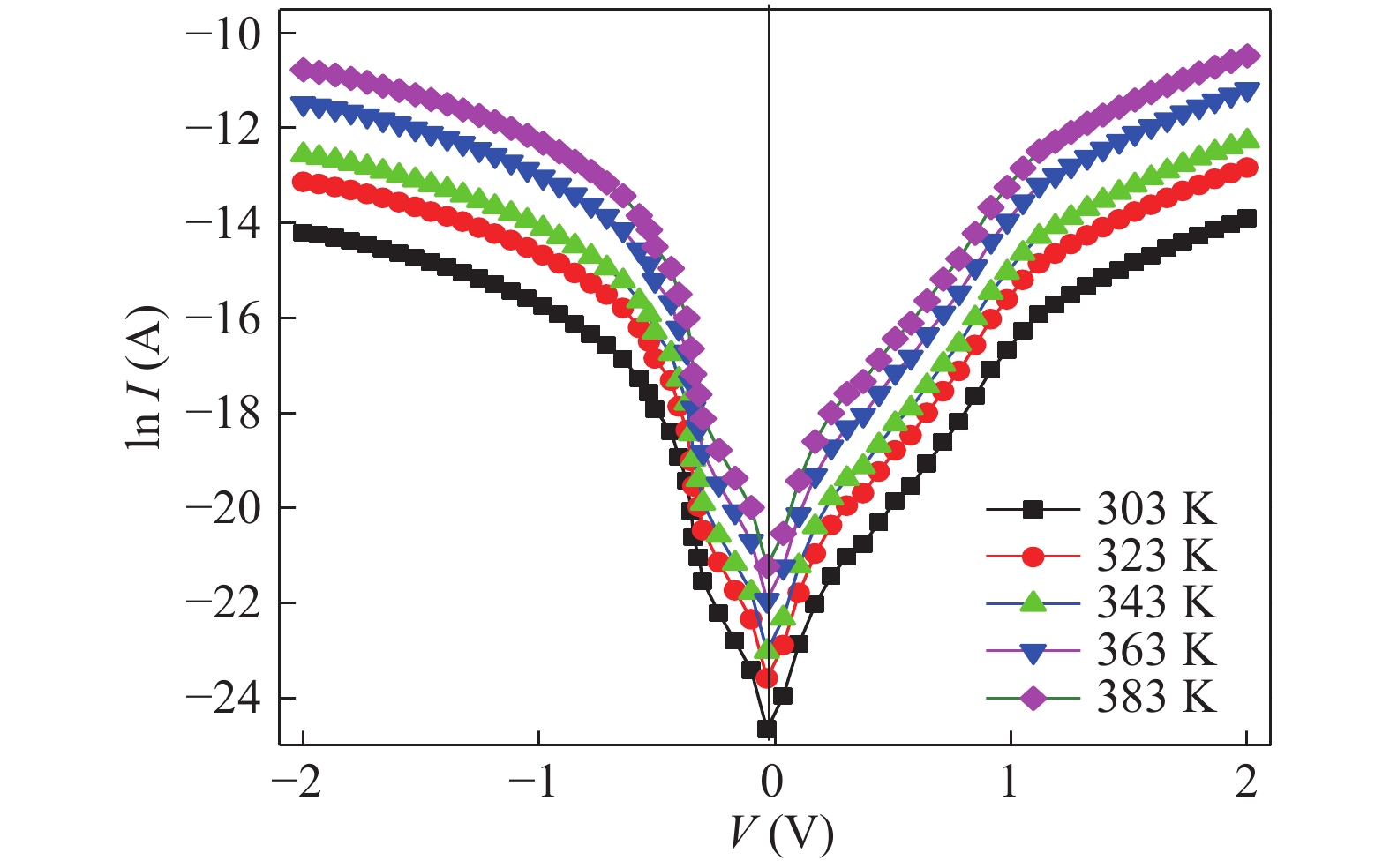
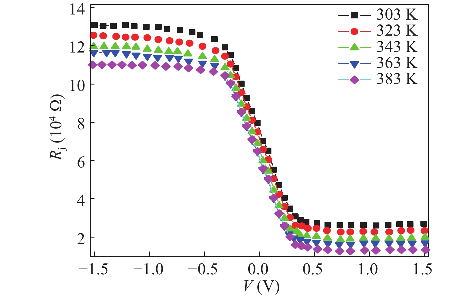
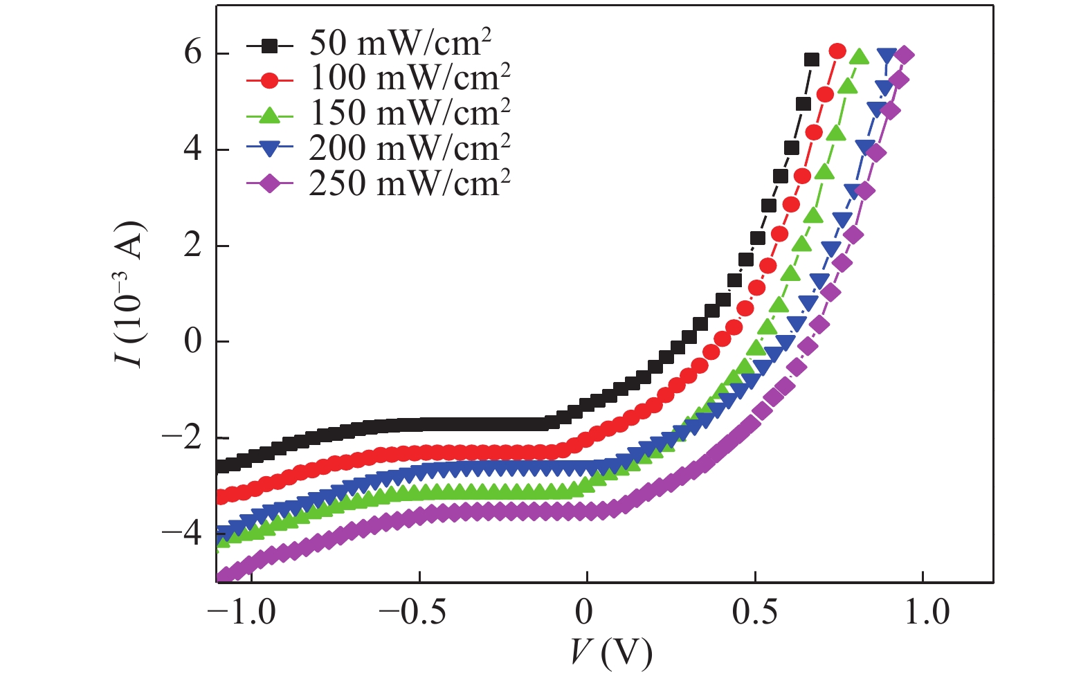
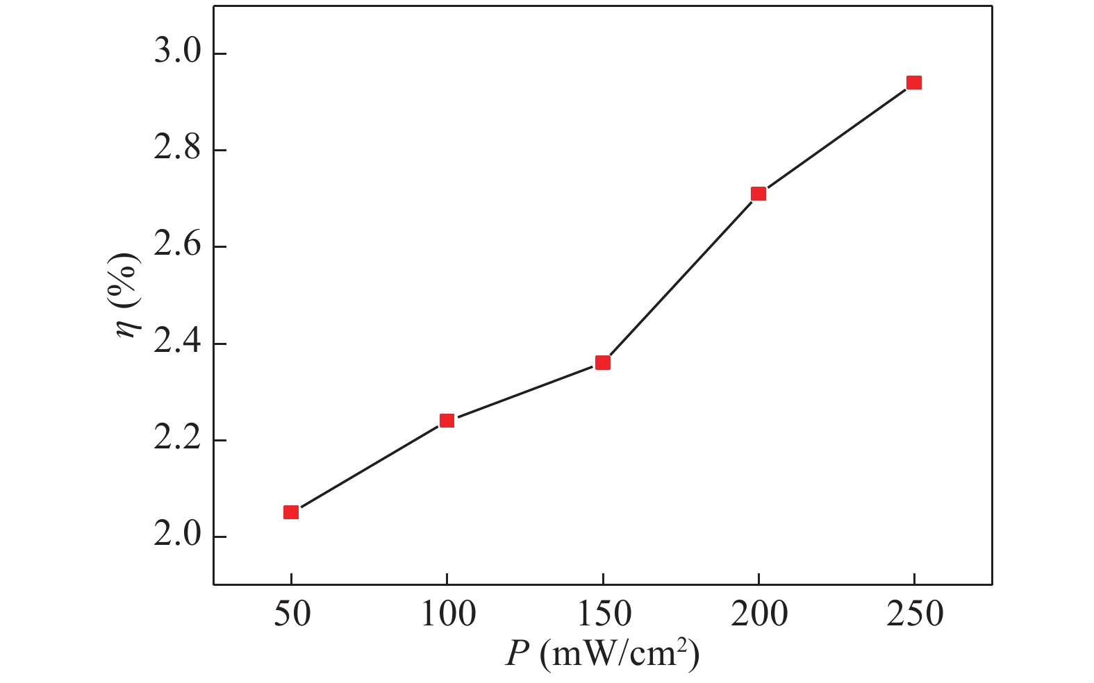
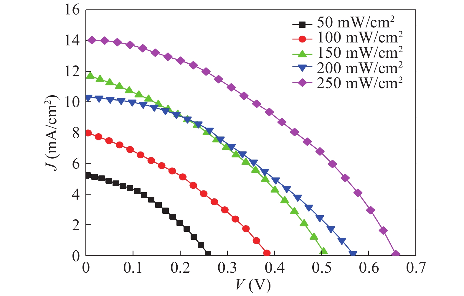
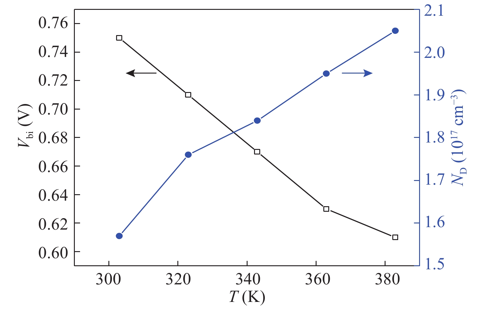
The CuInGeSe4 thin film was deposited onto n-type single crystal silicon wafers by the electron beam deposition technique. The Au/CuInGeSe4/n-Si/Al heterojunction device has been fabricated. The structure of the CuInGeSe4 thin film was characterized by X-ray diffraction (XRD), scanning electron microscope (SEM), and energy dispersive X-ray analysis (EDX). The dark current–voltage characteristics of the Au/CuInGeSe4/n-Si/Al heterojunction diode have been studied at a temperature range of 303–383 K. Also, the photovoltaic properties were examined at different illumination intensities. The capacitance–voltage characteristics of the CuInGeSe4/n-Si heterojunction were studied at different temperatures in the dark.

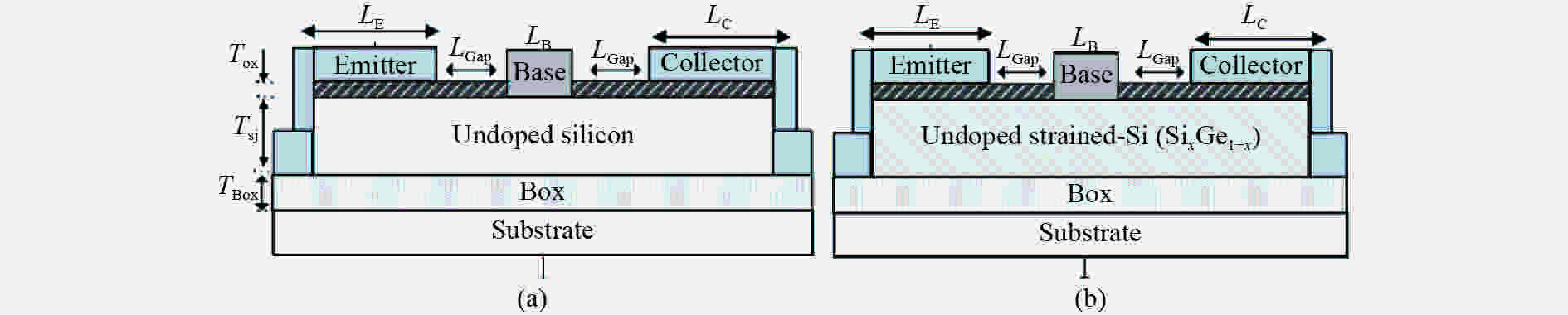
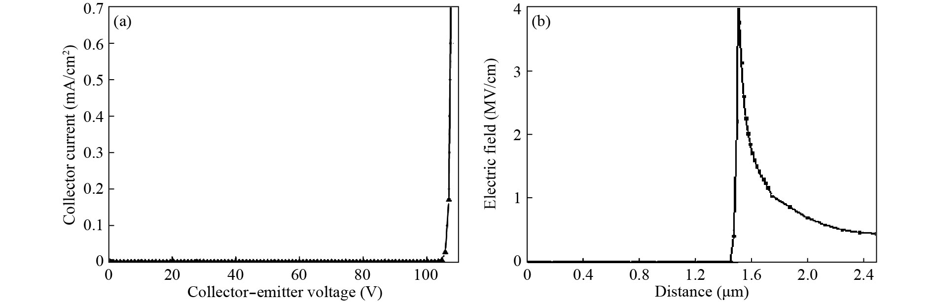
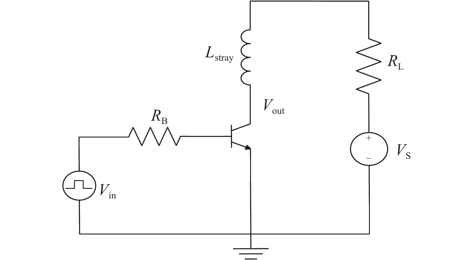
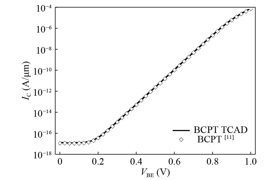
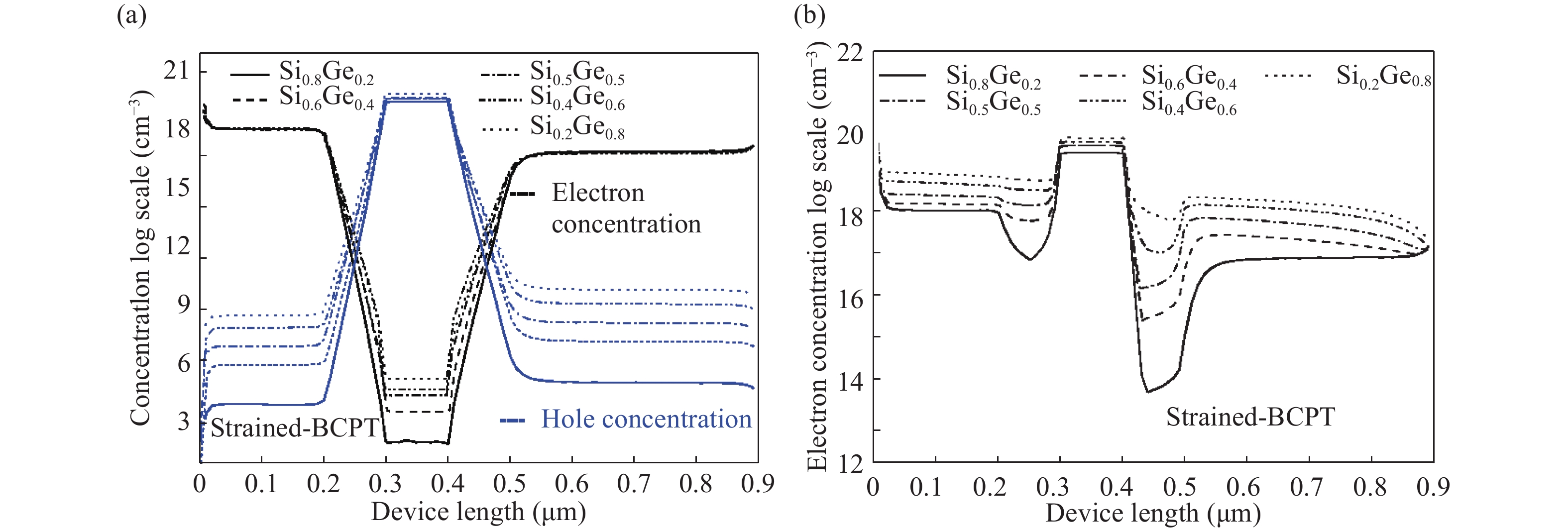
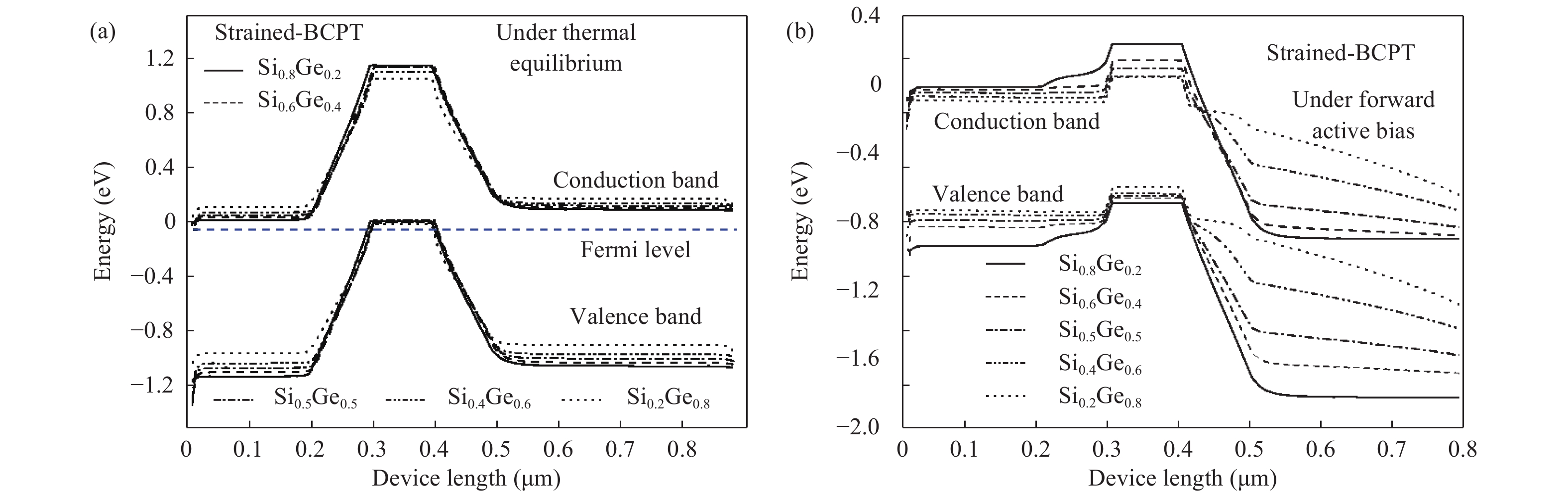
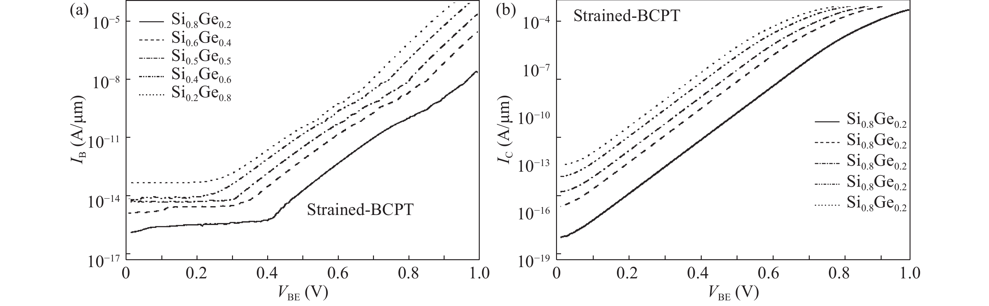
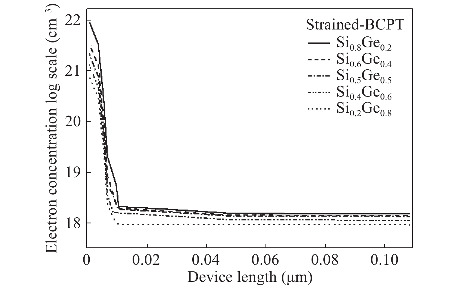
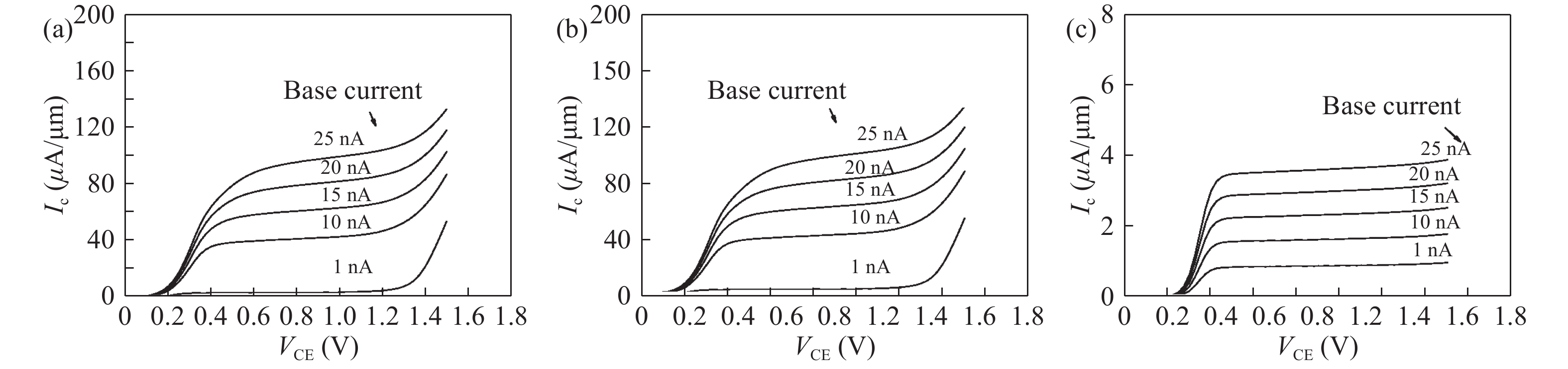
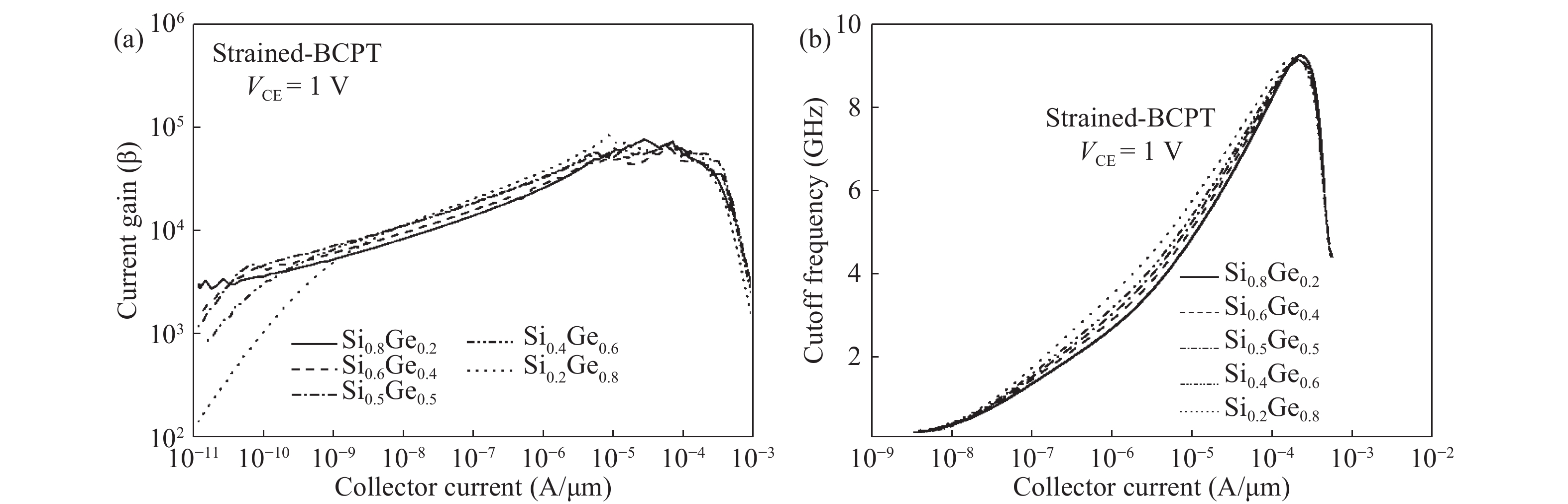
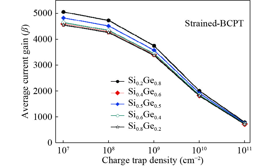
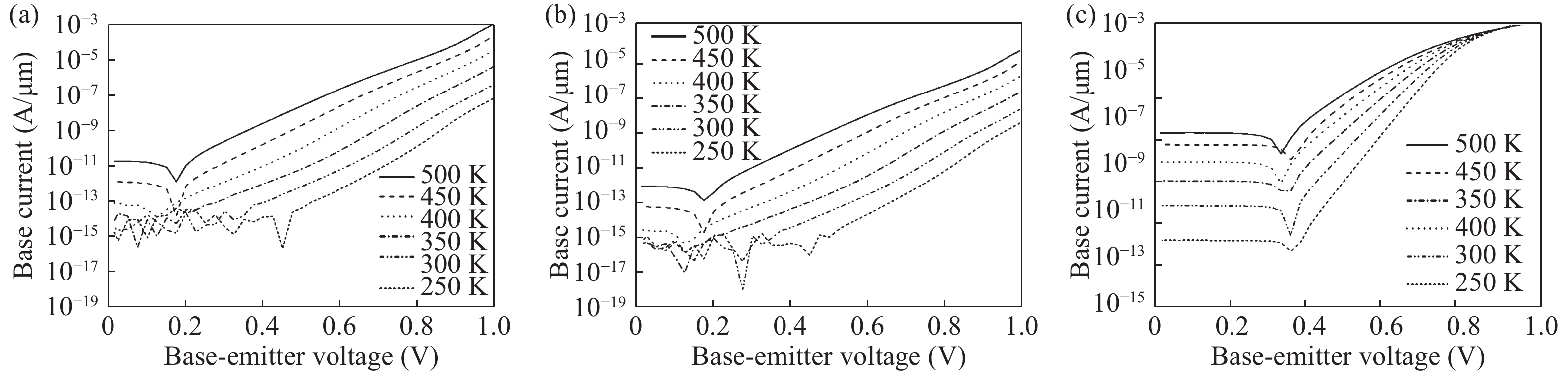
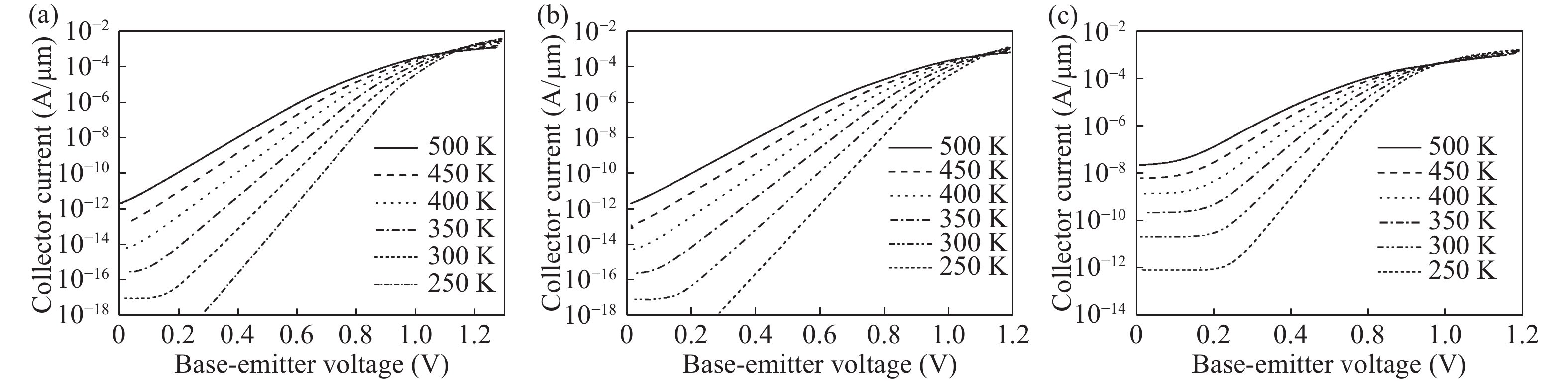
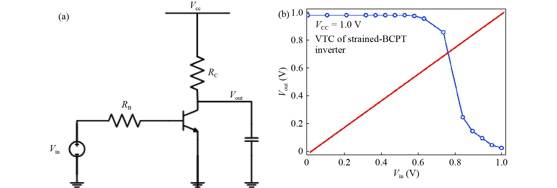
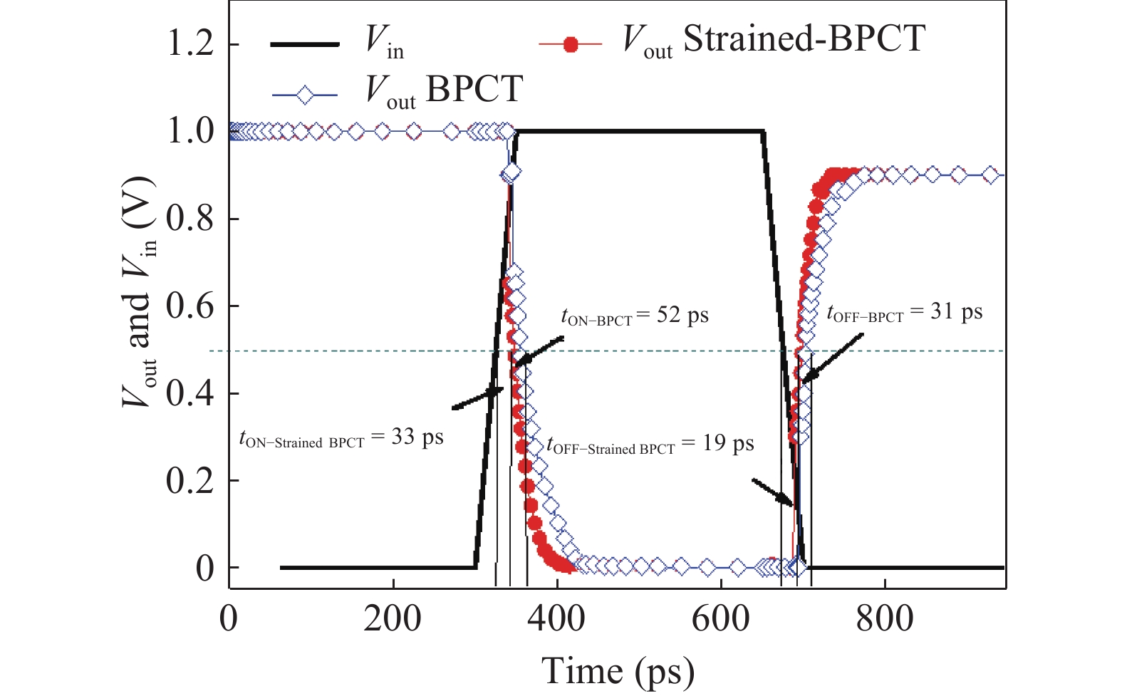
In this manuscript we analyze a unique approach to improve the performance of the bipolar charge plasma transistor (BCPT) by introducing a strained Si/SixGe1−x layer as the active device region. For charge plasma realization different metal work-function electrodes are used to induce n+ and p+ regions on undoped strained silicon-on-insulator (sSOI or SixGe1−x) to realize emitter, base, and collector regions of the BCPT. Here, by using a calibrated 2-D TCAD simulation the impact of a Si mole fraction x (in SixGe1−x) on device performance metrics is investigated. The analysis demonstrates the band gap lowering with decreasing Si content or effective strain on the Si layer, and its subsequent advantages. This work reports a significant improvement in current gain, cutoff frequency, and lower collector breakdown voltage (BVCEO) for the proposed structure over the conventional device. The effect of varying temperature on the strained Si layer and its implications on the device performance is also investigated. The analysis demonstrates a fair device-level understanding and exhibits the immense potential of the SixGe1−x material as the device layer. In addition to this, using extensive 2-D mixed-mode TCAD simulation, a considerable improvement in switching transient times are also observed compared to its conventional counterpart.

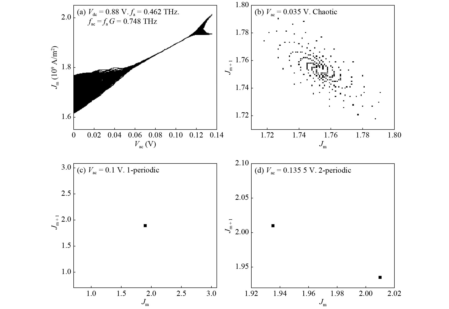
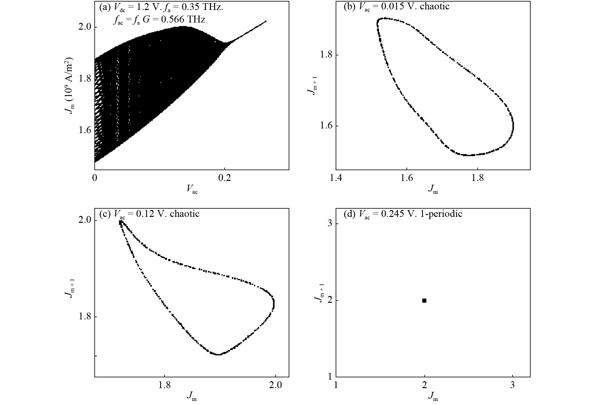
By using the time-dependent hydrodynamic equations, we carry out a theoretical study of nonlinear dynamics in an n+nn+ double-layer graphene diode driven by terahertz radia-tion. A cooperative nonlinear oscillatory mode shows up due to the negative differential conductance effect. We use different chaos-detecting methods, such as the Poincaré bifurcation diagram and the first return map, to examine the transitions between the periodic and chaotic states. The double-layer graphene diode shows typical nonlinear dynamical behavior with the DC bias, AC amplitudes and the AC frequency as the control parameters.
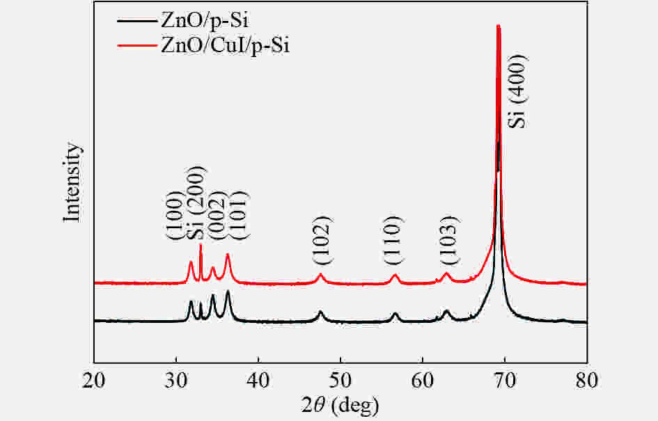
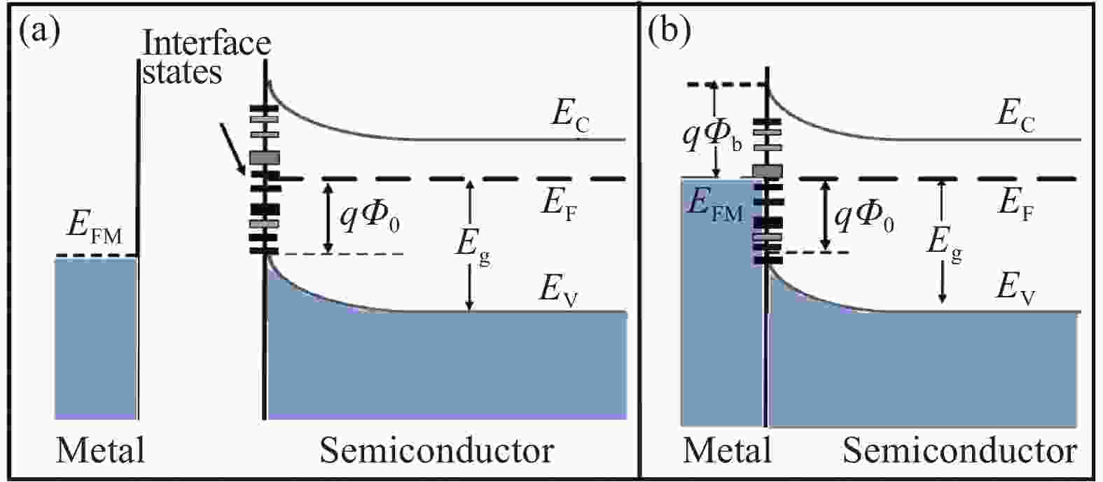
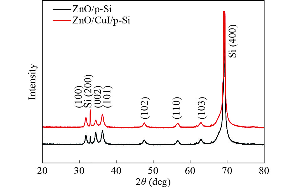
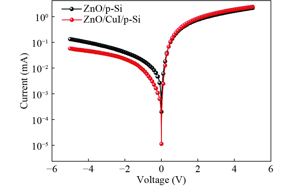
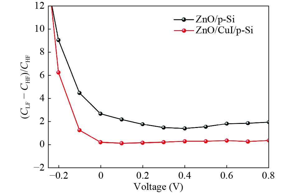
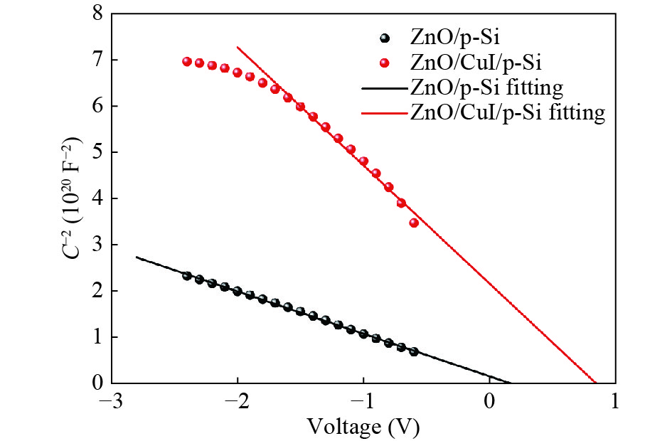
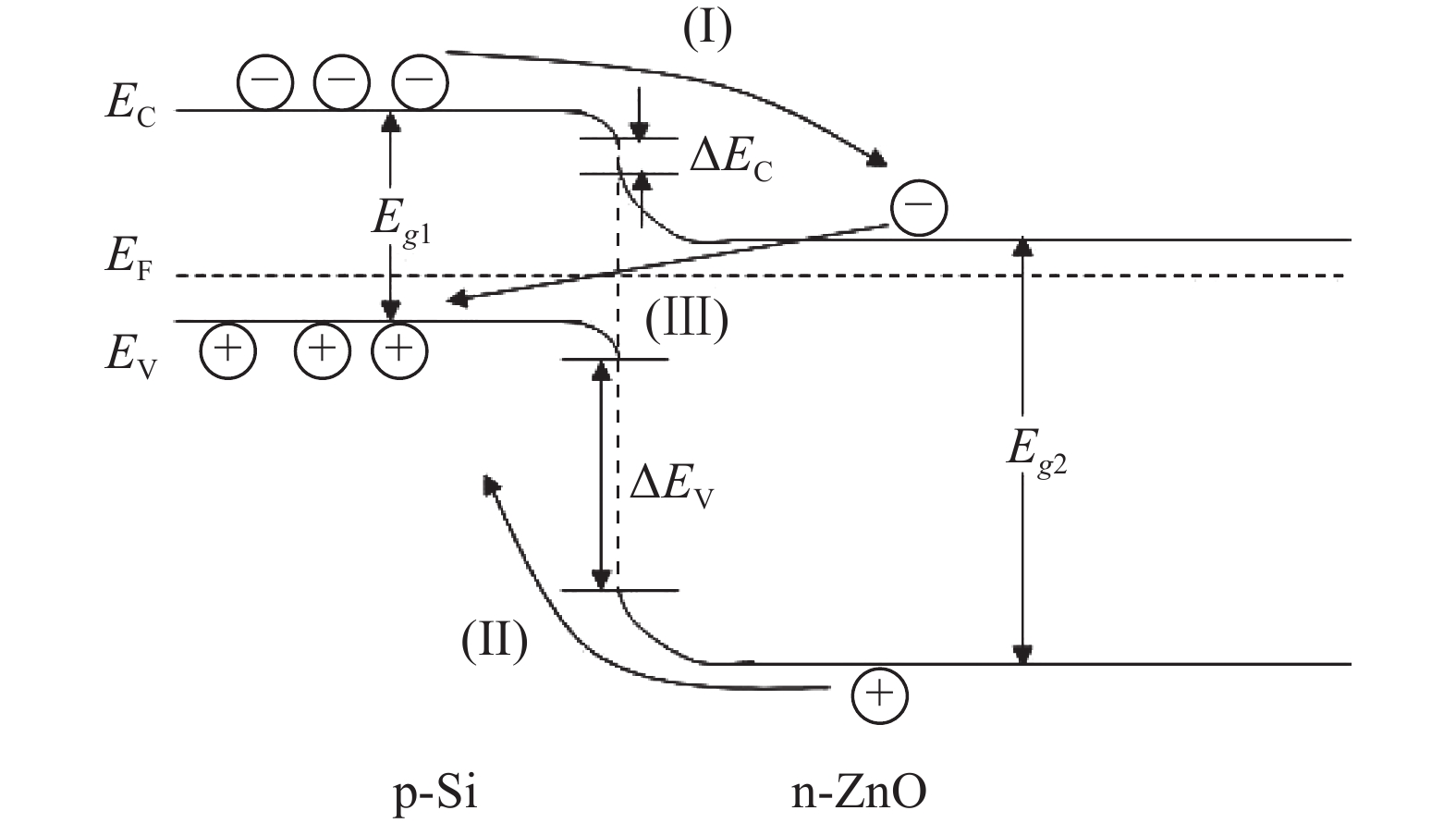
The ZnO/Si heterojunction diode can be integrated with the Si process, which has attracted great attention in recent years. However, the large number of interface states at the ZnO/ Si heterojunction interface could adversely affect its optoelectronic properties. Here, n-type ZnO thin film was deposited on p-Si substrate for formation of an n-ZnO/p-Si heterojunction substrate. To passivate the ZnO/Si interface, a thin CuI film interface passivation layer was inserted at the ZnO/p-Si heterojunction interface. Electrical characterization such as I–V and C–V characteristic curves confirmed the significant improvement of the heterojunction properties e.g. enhancement of forward current injection, reduction of reverse current and improvement of the rectification ratio. These results showed that the passivation of interface is critical for ZnO/Si heterojunctions.
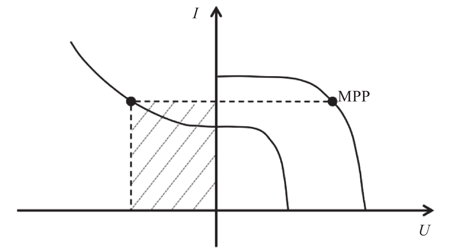
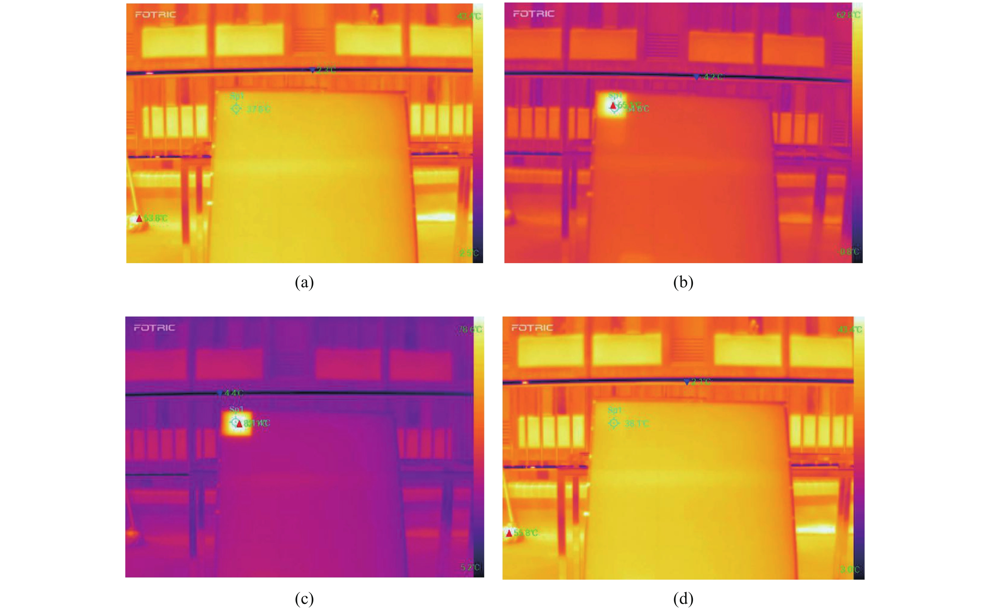
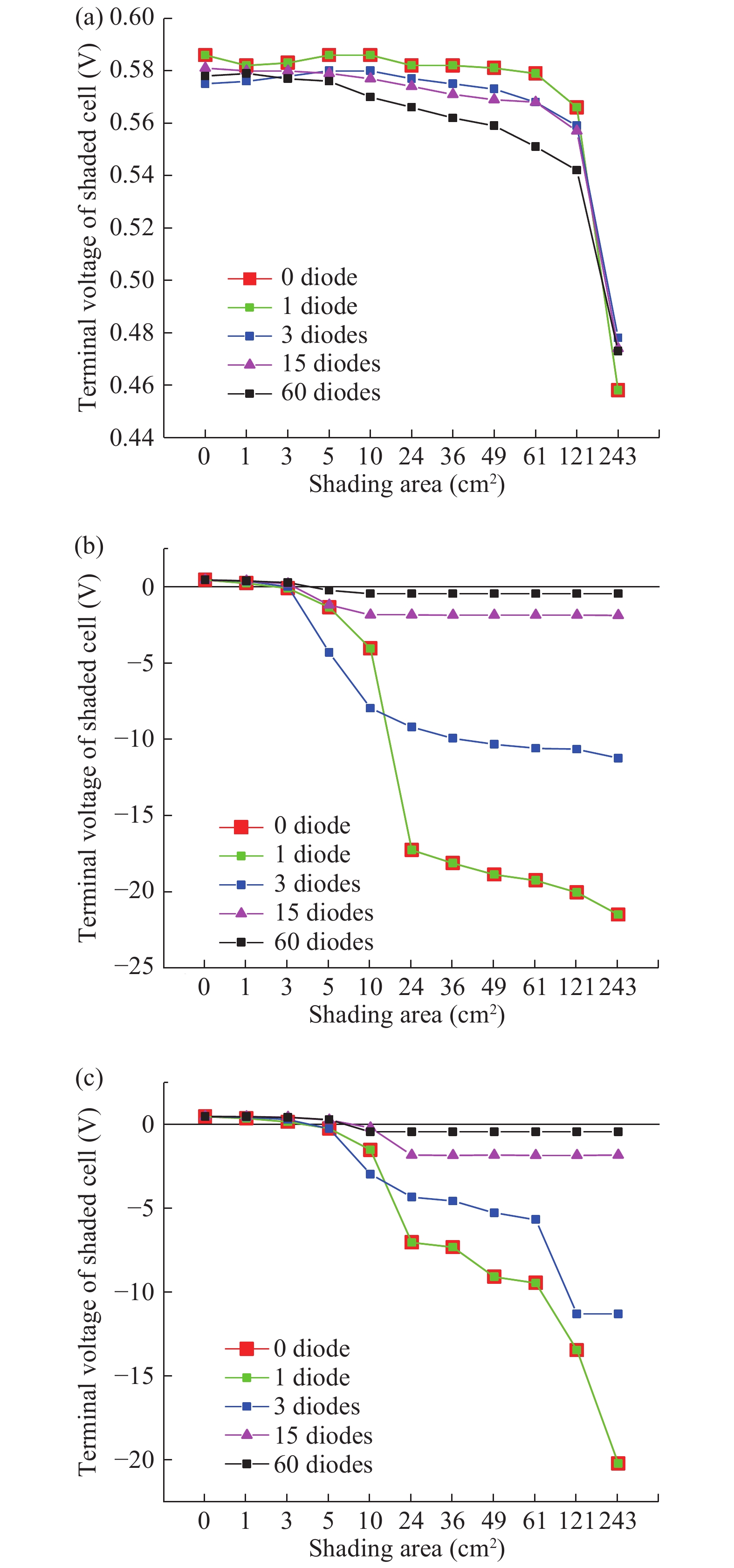
A hot spot is a reliability problem in photovoltaic (PV) modules where a mismatched or shaded cell heats up significantly and degrades the PV module output power performance. High PV cell temperature due to a hot spot can damage the cell encapsulate and lead to second breakdown, which both cause permanent damage to the PV module. In present systems, bypass diodes are used to mitigate the hot spot problem. In this work, five commercial polysilicon PV modules configured with different numbers of bypass diodes are used to study the influence of bypass diodes on the reverse bias voltage of a shaded cell and the resulting hot spot phenomenon. The reverse bias voltage of the shaded cell, and the hot spot probability and severity decrease as the number of bypass diodes increases. Negative terminal voltage of a shaded cell accompanied by a switched-off bypass diode are the necessary condition for hot spot generation. In an extreme case where each cell has an individual bypass diode in a PV module, it still cannot avoid the hazards of a hot spot under the shading areas of 5–7 cm2, but the probability of a hot spot is reduced to a minimum of 0.41%.

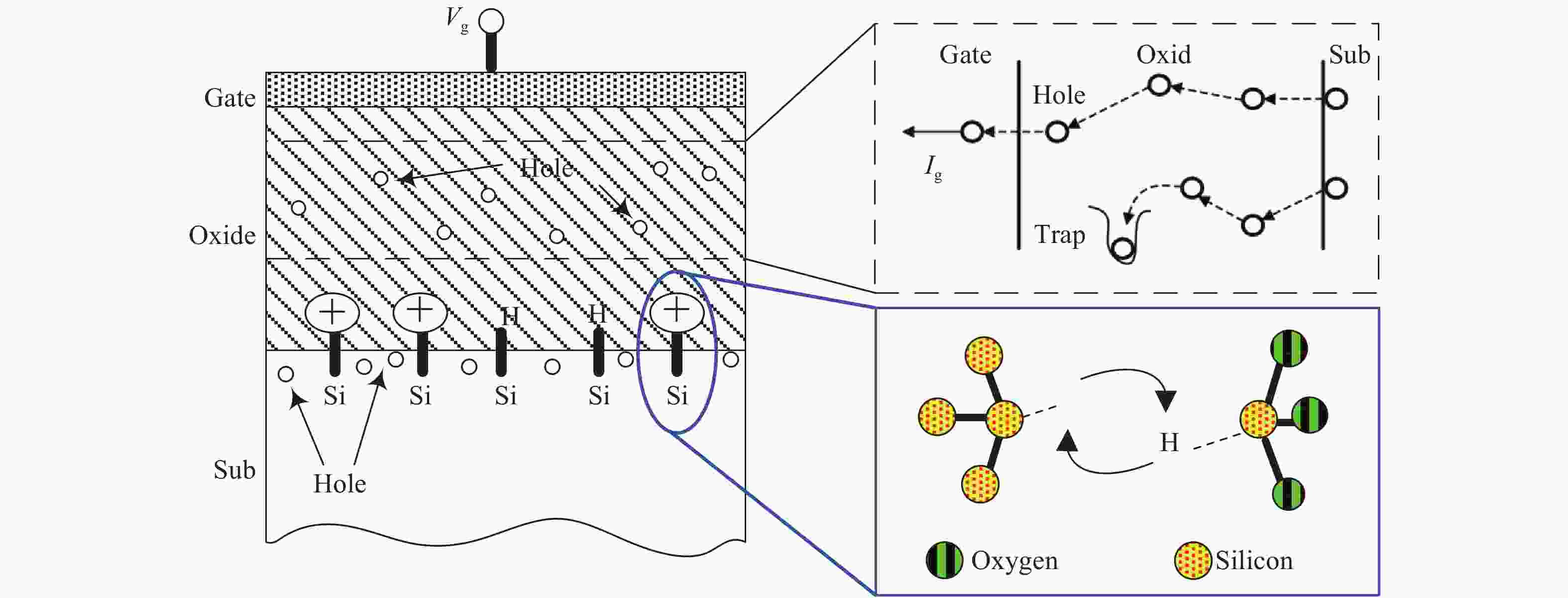
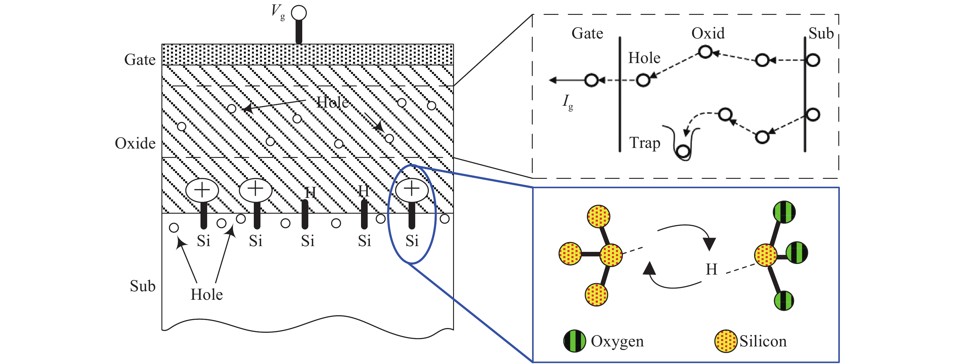
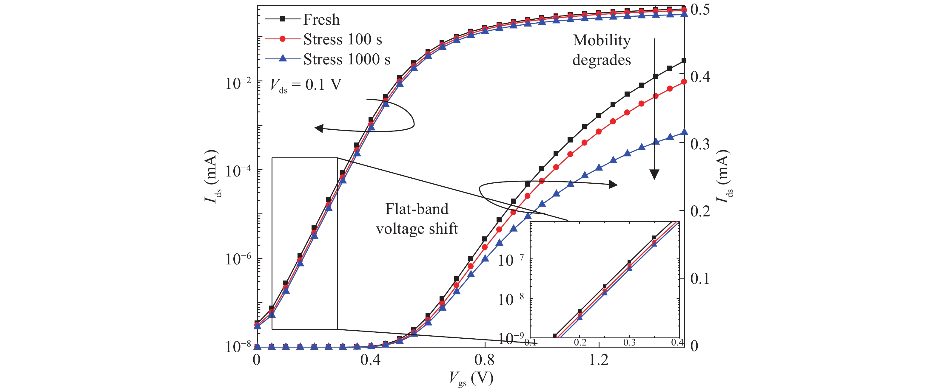
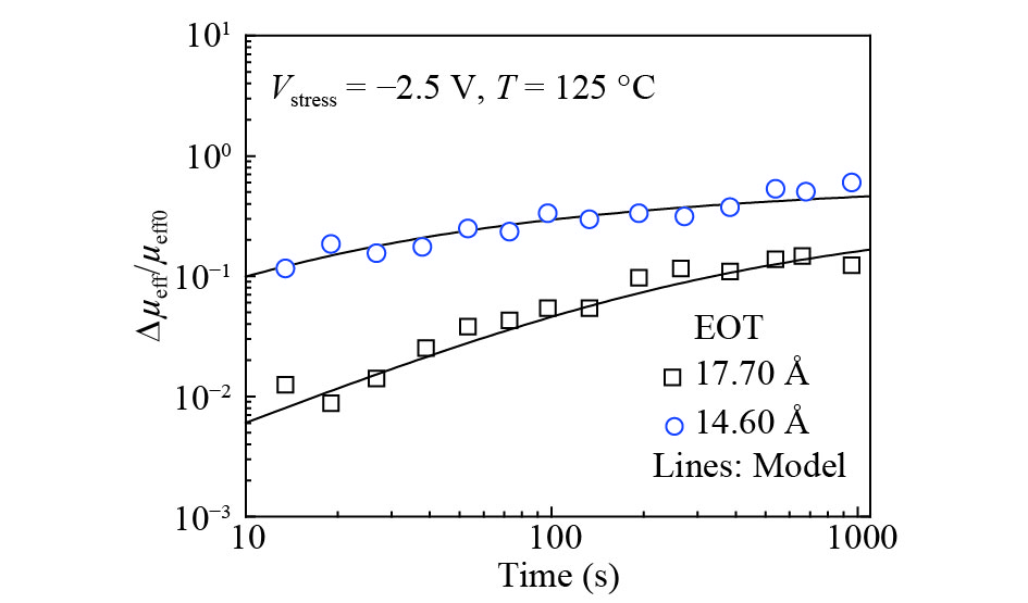
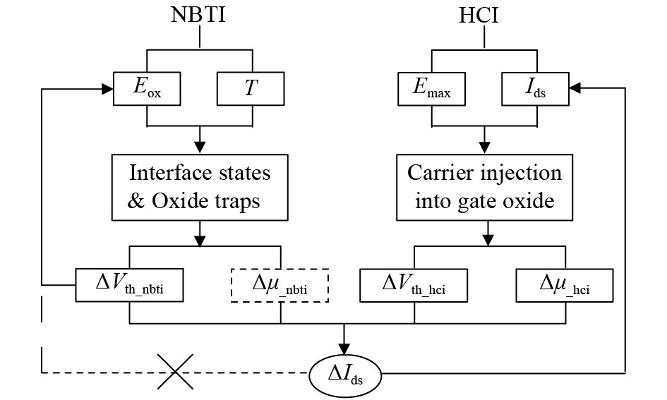
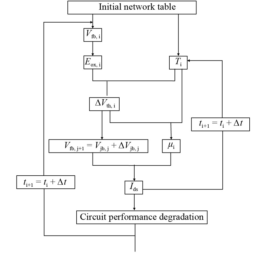
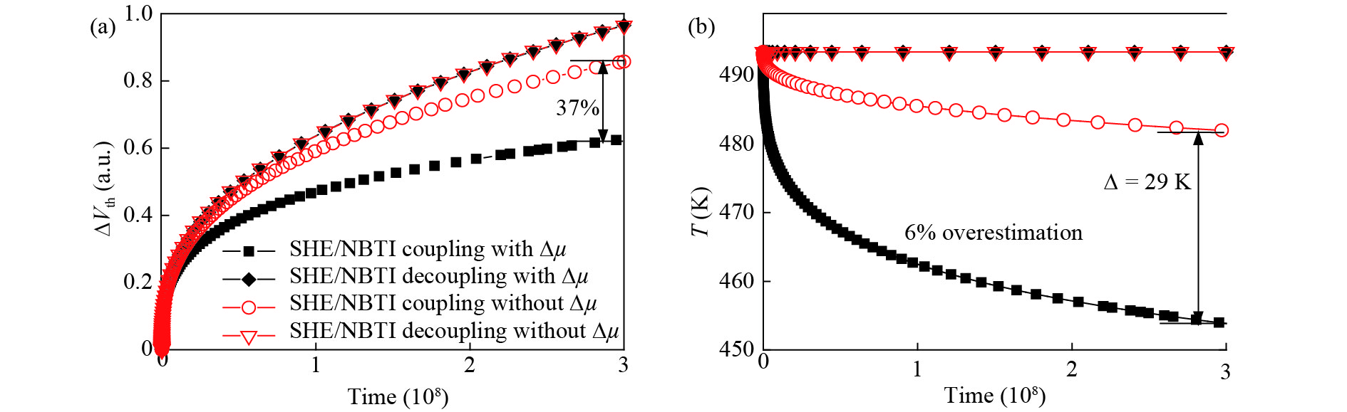
The mobility degradation induced by negative bias temperature instability (NBTI) is usually ignored in traditional NBTI modeling and simulation, resulting in overestimation of the circuit lifetime, especially after long-term operation. In this paper, the mobility degradation is modeled in combination with the universal NBTI model. The coulomb scattering induced by interface states is revealed to be the dominant component responsible for mobility degradation. The proposed mobility degradation model fits the measured data well and provides an accurate solution for evaluating coupling of NBTI with HCI (hot carrier injection) and SHE (self-heating effect), which indicates that mobility degradation should be considered in long-term circuit aging simulation.


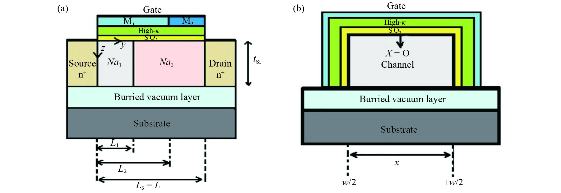
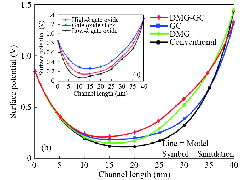
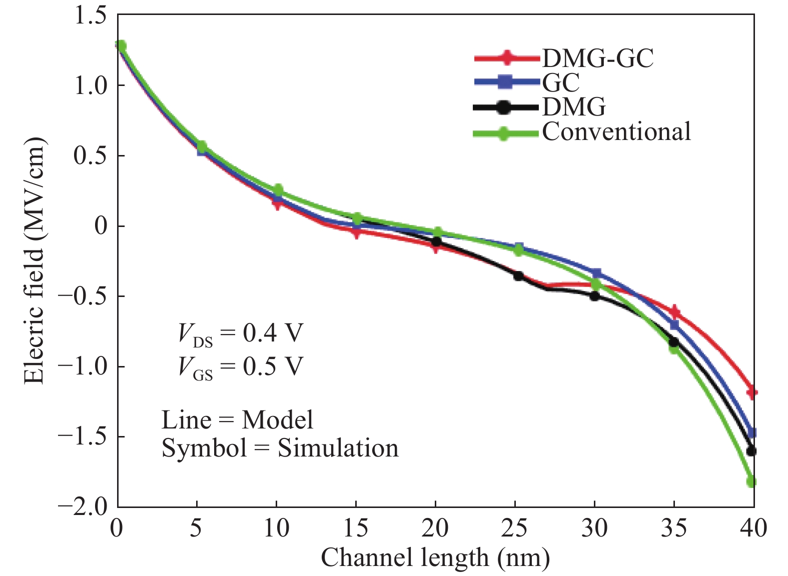
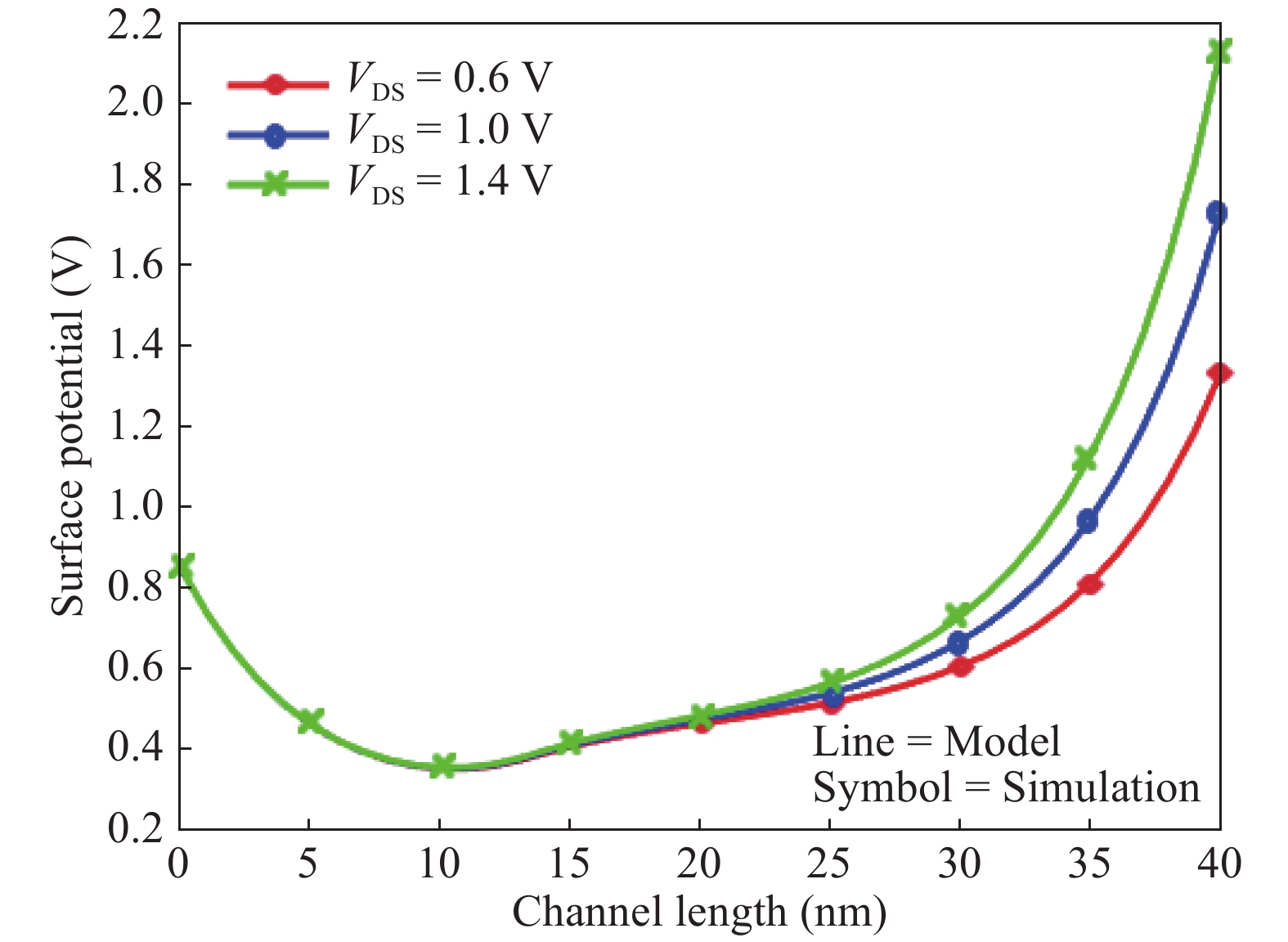
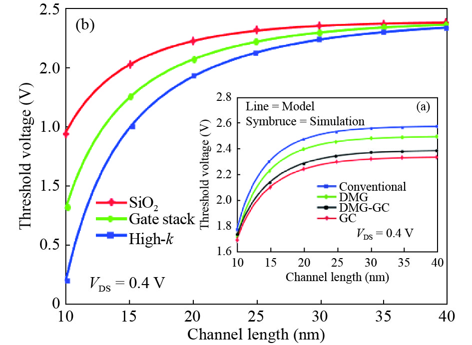
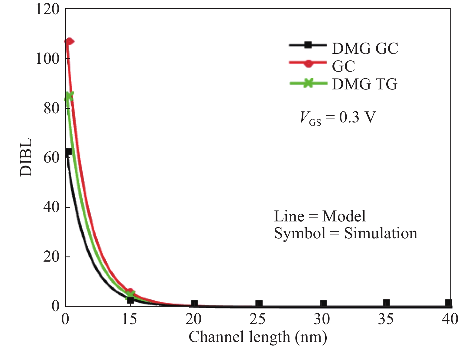
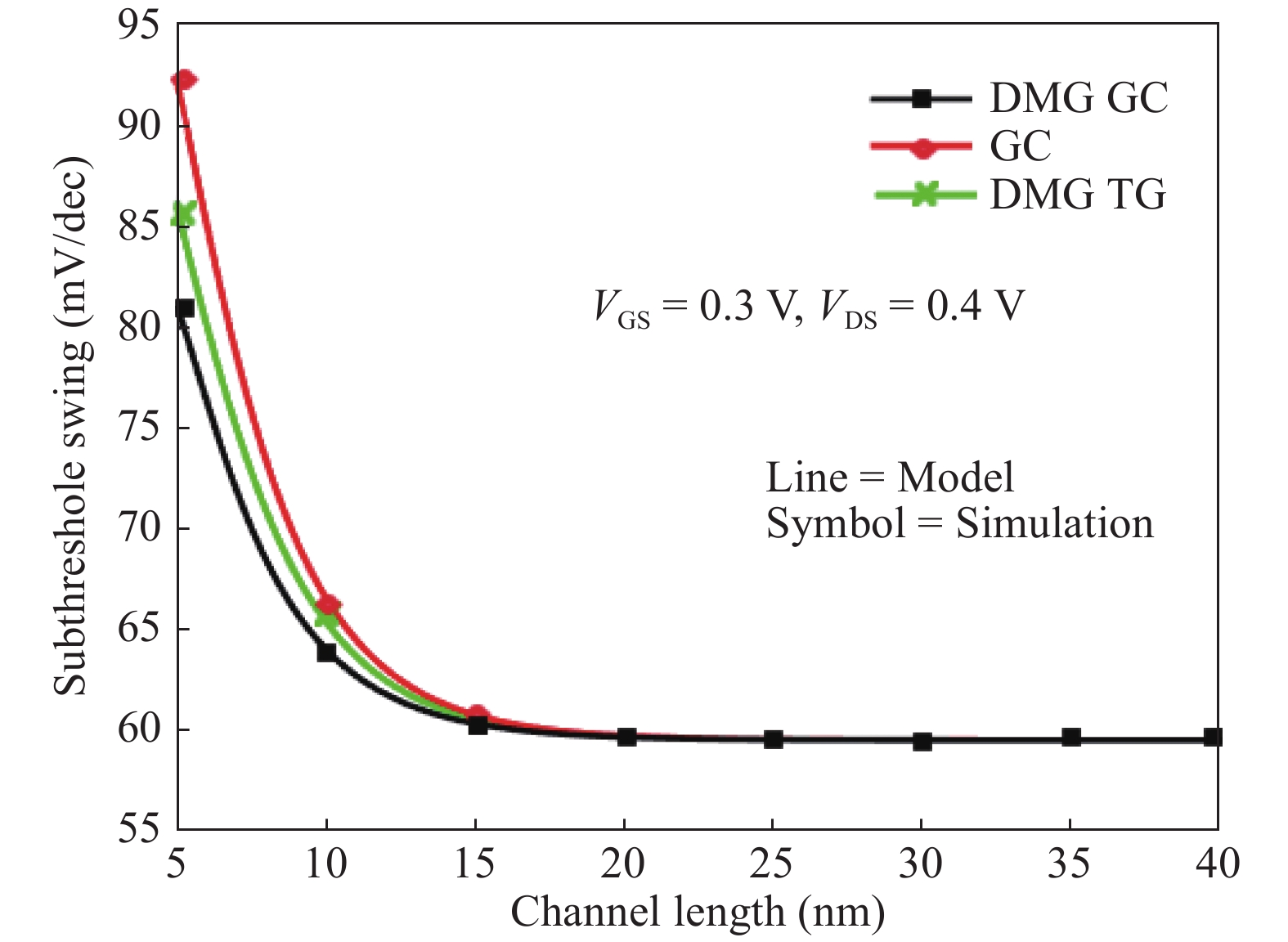
The evolution of the traditional metal oxide semiconductor field effect transistor (MOSFET) from planar single gate devices into 3D multiple gates has led to higher package density and high current drive. However, due to continuous scaling and as a consequent close proximity between source and drain in the nano-regime, these multigate devices have been found to suffer from performance degrading short channel effects (SCEs). In this paper, a three dimensional analytical model of a trigate MOSFET incorporating non-conventional structural techniques like silicon-on-insulator, gate and channel engineering in addition to gate oxide stack is presented. The electrostatic integrity and device capability of suppressing SCEs is investigated by deriving the potential distribution profile using the three dimensional Poisson’s equation along with suitable boundary conditions. The other device parameters like threshold voltage and subthreshold swing are produced from the surface potential model. The validity of the proposed structure is established by the close agreement among the results obtained from the analytical model and simulation results.
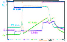
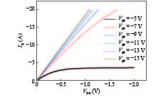
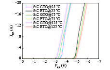
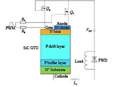
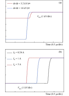
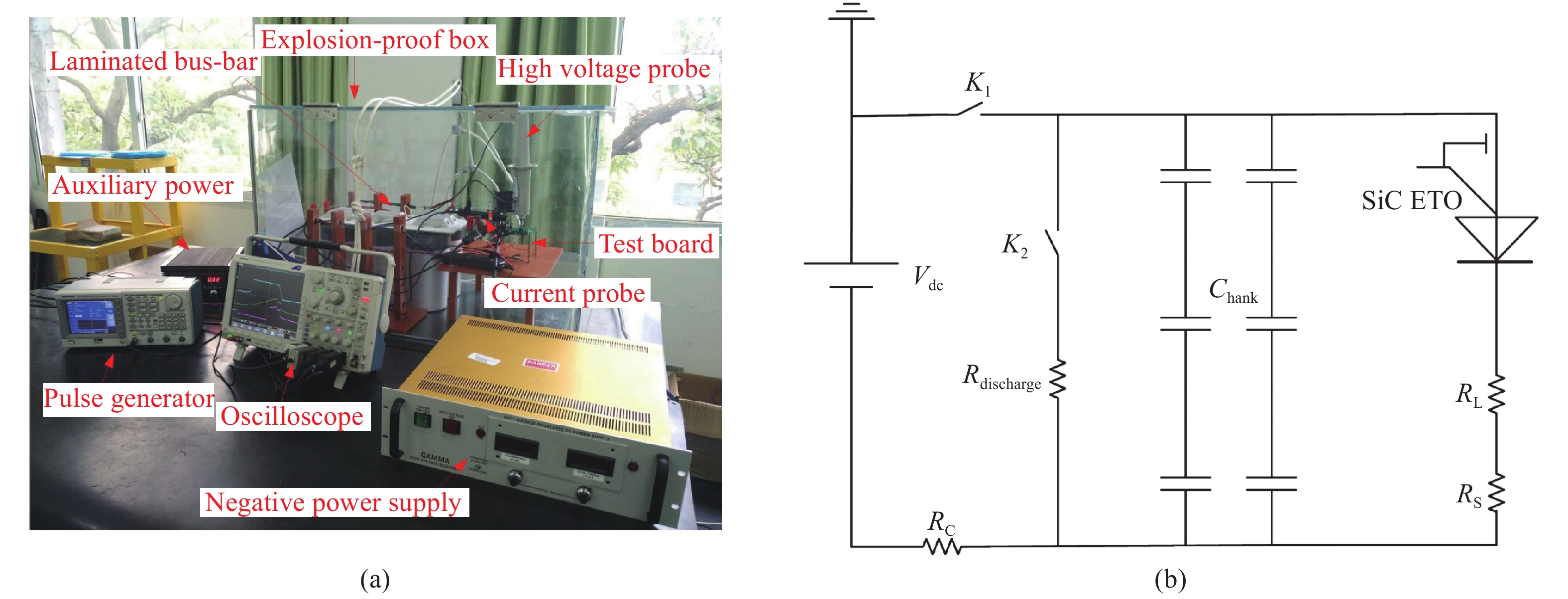
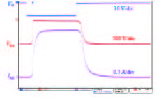
Silicon carbide (SiC) emitter turn-off thyristors (ETOs) are very promising high power capacity semiconductor devices for high voltage and high power density power systems and pulse power applications. However, reports on comparison of high voltage SiC GTOs and ETOs in pulse power applications have been rare. In this paper, a comprehensive study on a 6.5 kV SiC GTO and ETO are carried out to demonstrate the superior performance of the SiC ETO over the GTO in pulse power application. A 6.5 kV SiC ETO was designed and tested with a printed circuit board (PCB) integrated gate driver. The forward conduction characteristics of the SiC ETO and GTO in elevated temperatures are measured and compared, showing the excellent temperature coefficient of the SiC ETO's output characteristics. Their turn-off characteristics with resistive load are measured and compared, demonstrating that the SiC ETO has much faster switching speed and smaller turn-off loss. Experimental results demonstrate that the SiC ETO has a better performance, especially with respect to its switching characteristics, making it a very competitive candidate for high power and pulse power applications.


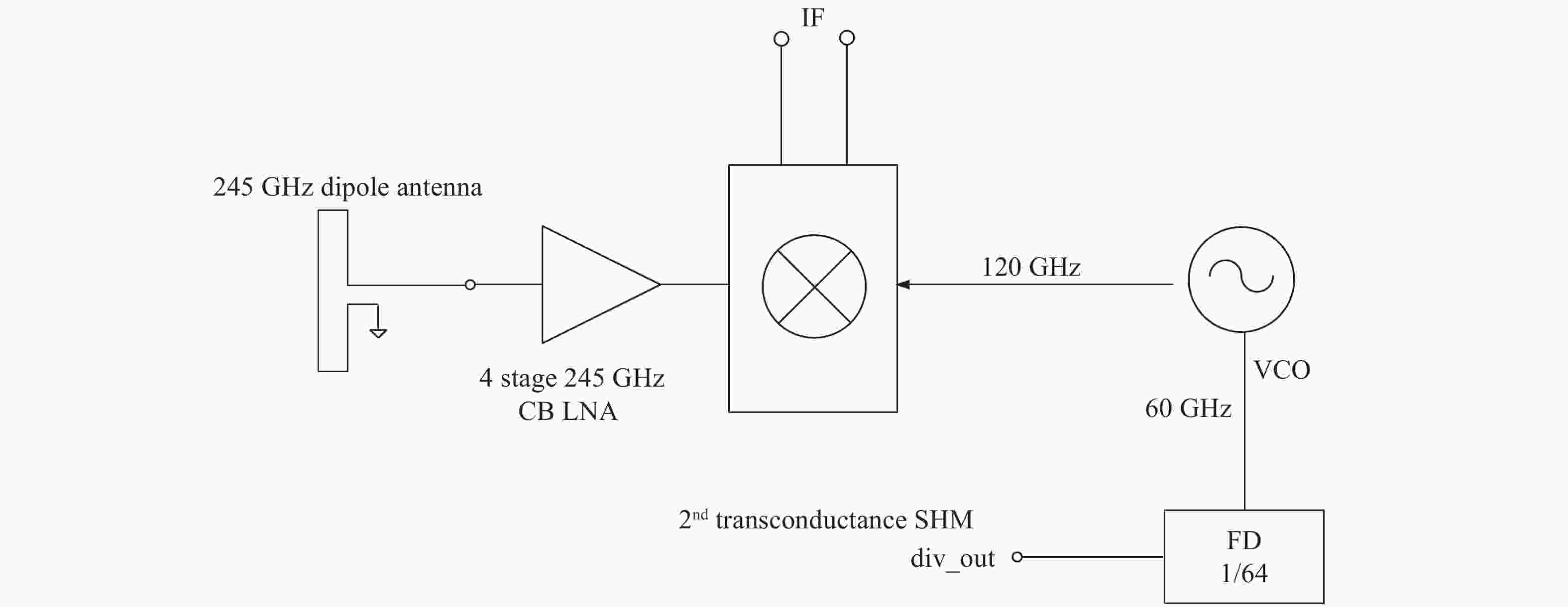
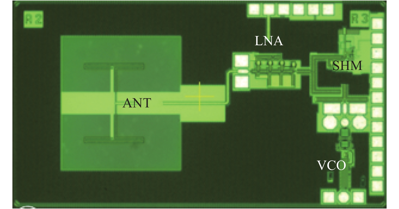
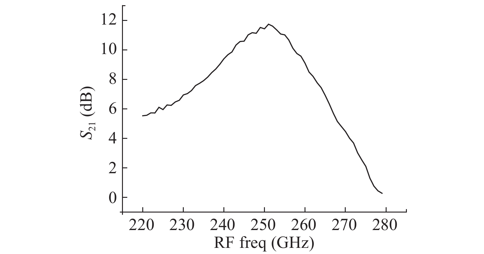
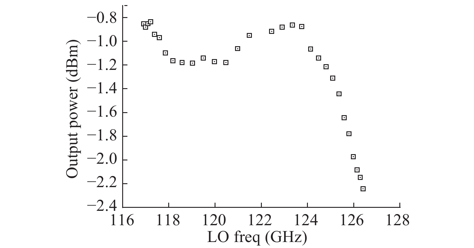
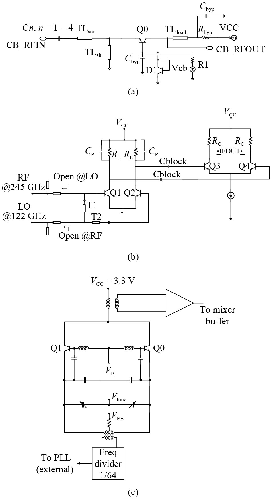
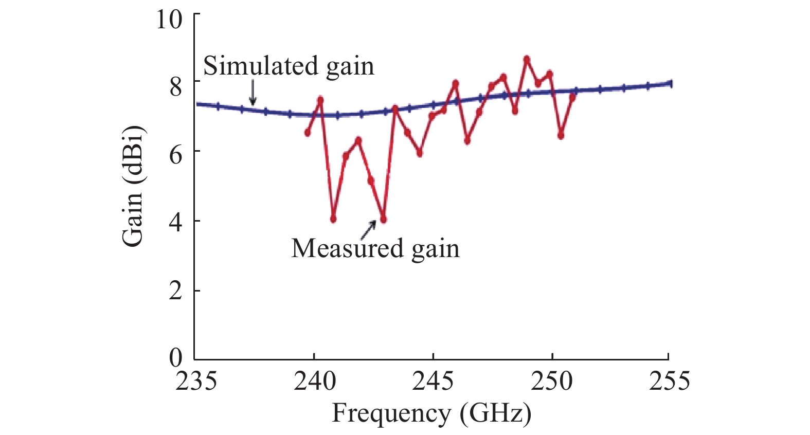
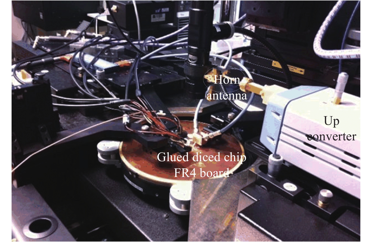
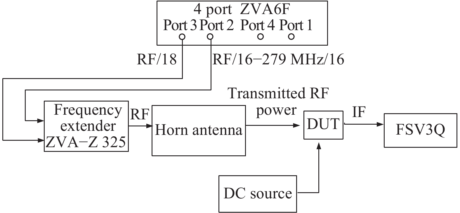
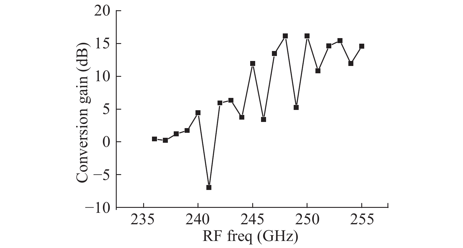
A 2nd transconductance subharmonic receiver for 245 GHz spectroscopy sensor applications has been proposed. The receiver consists of a 245 GHz on-chip folded dipole antenna, a CB (common base) LNA, a 2nd transconductance SHM (subharmonic mixer), and a 120 GHz push-push VCO with 1/64 divider. The receiver is fabricated in fT/fmax = 300/500 GHz SiGe:C BiCMOS technology. The receiver dissipates a low power of 288 mW. Integrated with the on-chip antenna, the receiver is measured on-chip with a conversion gain of 15 dB, a bandwidth of 15 GHz, and the chip will be utilized in PCB board design for gas spectroscopy sensor application.


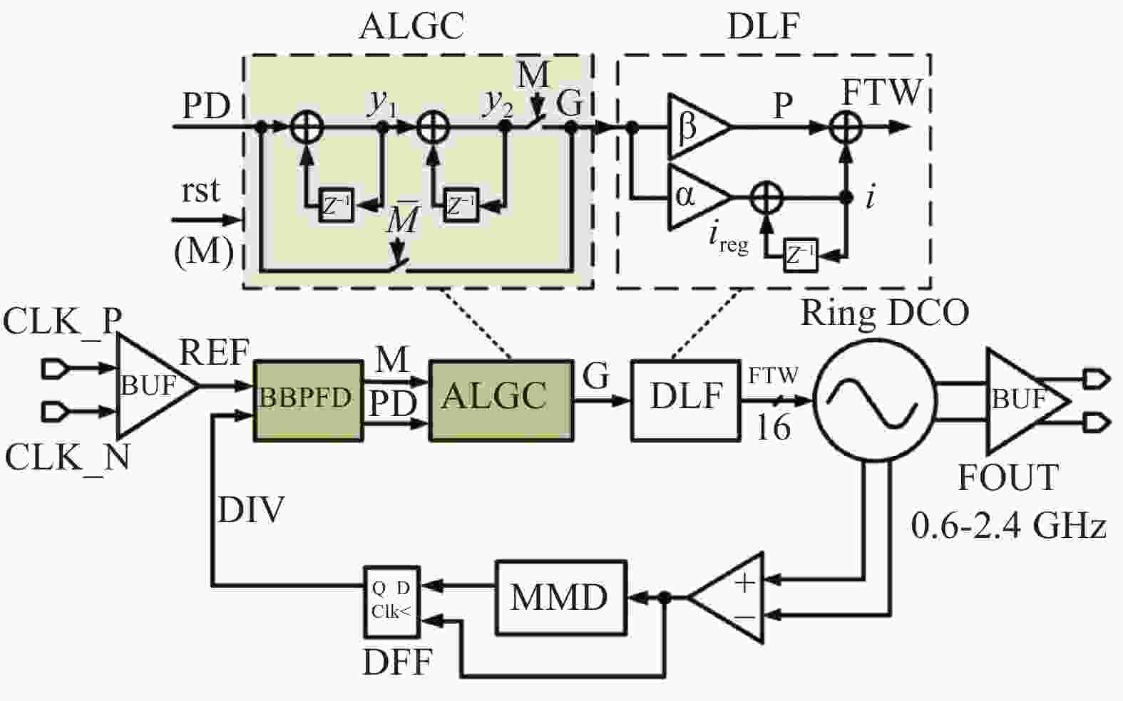
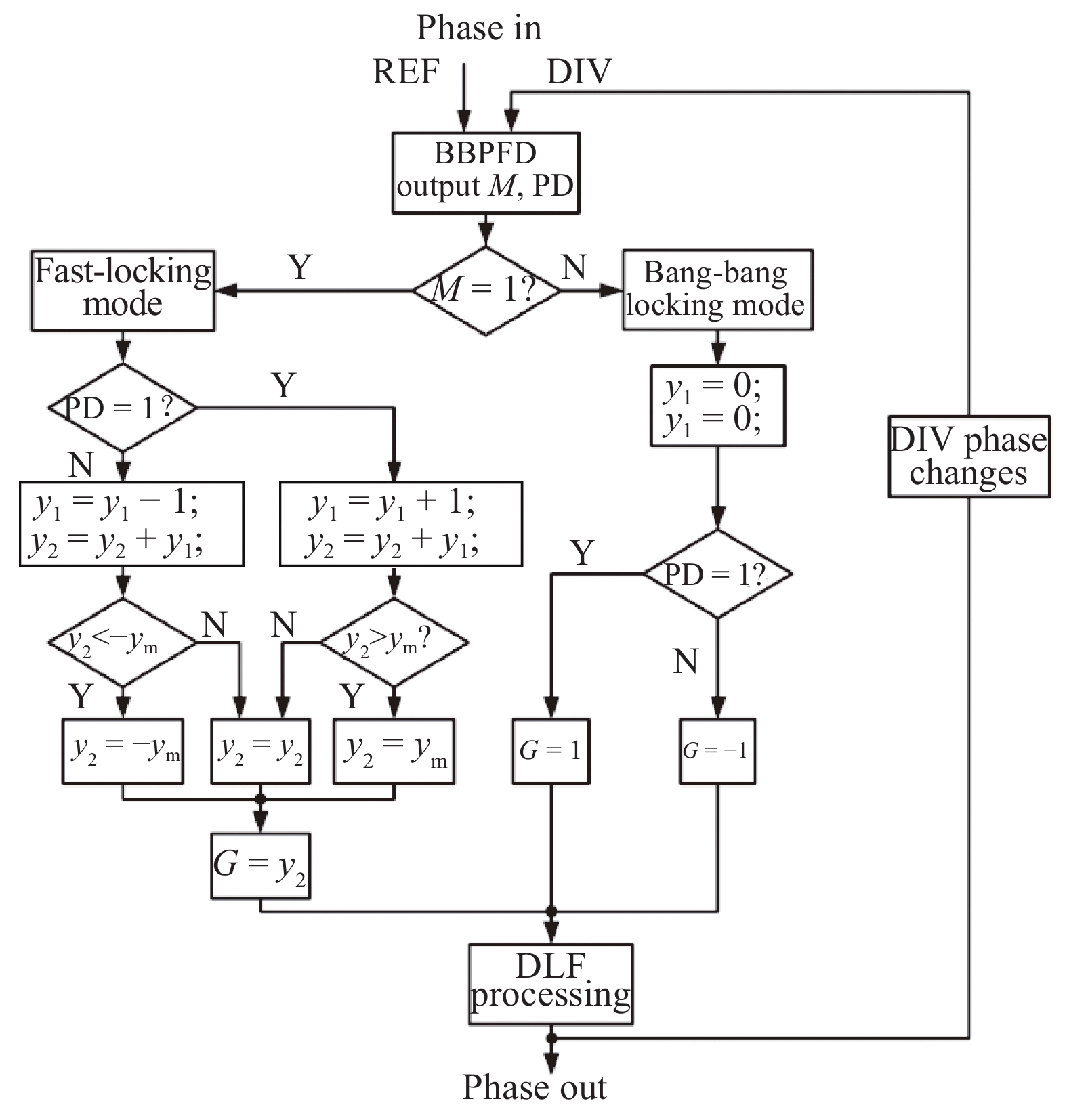
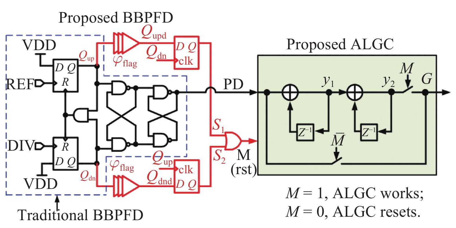
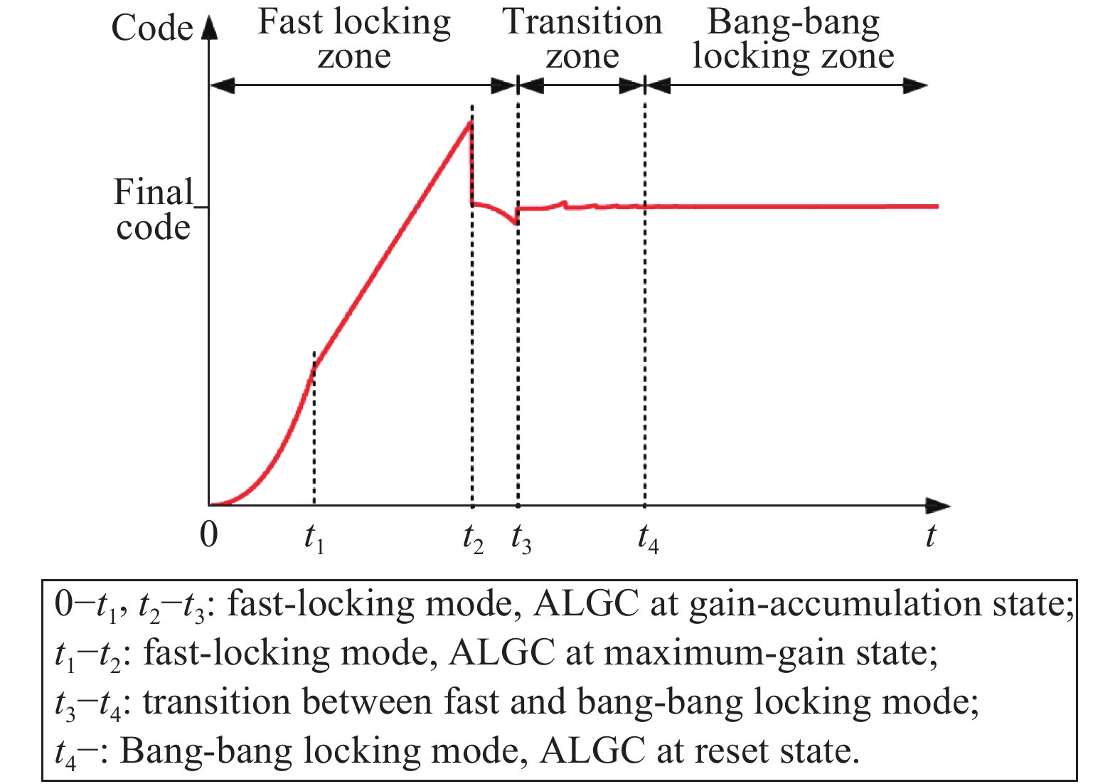
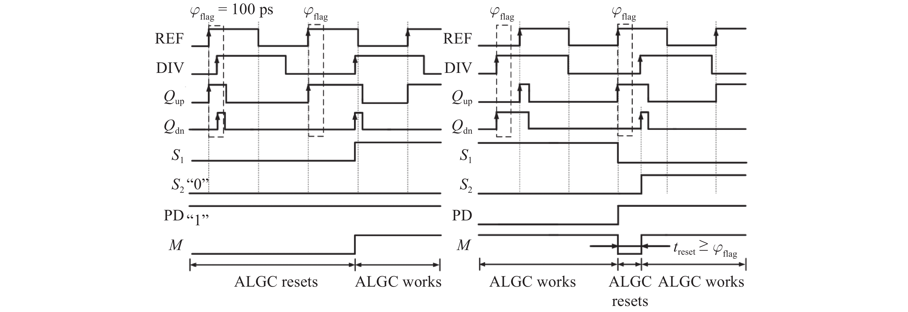
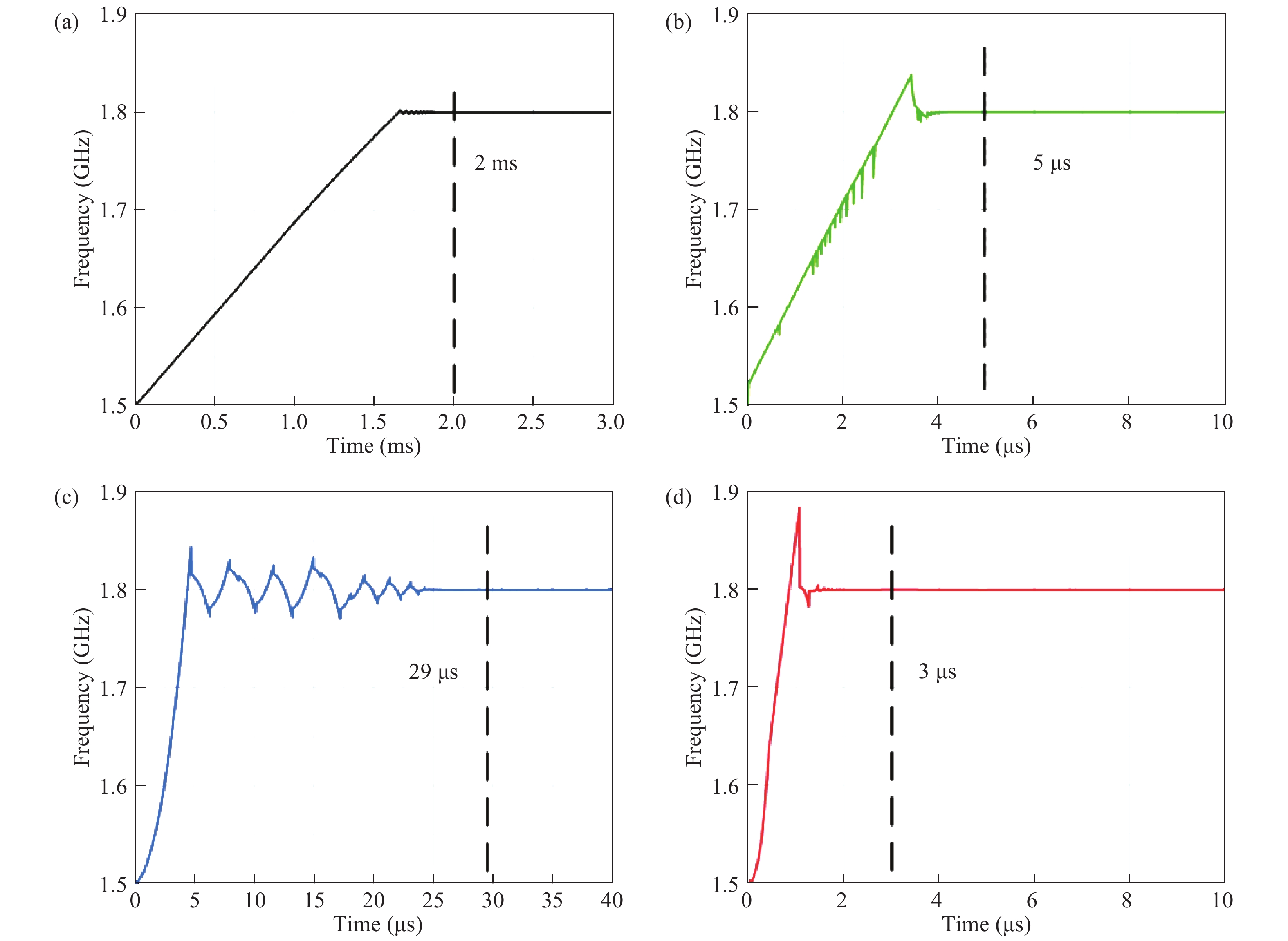
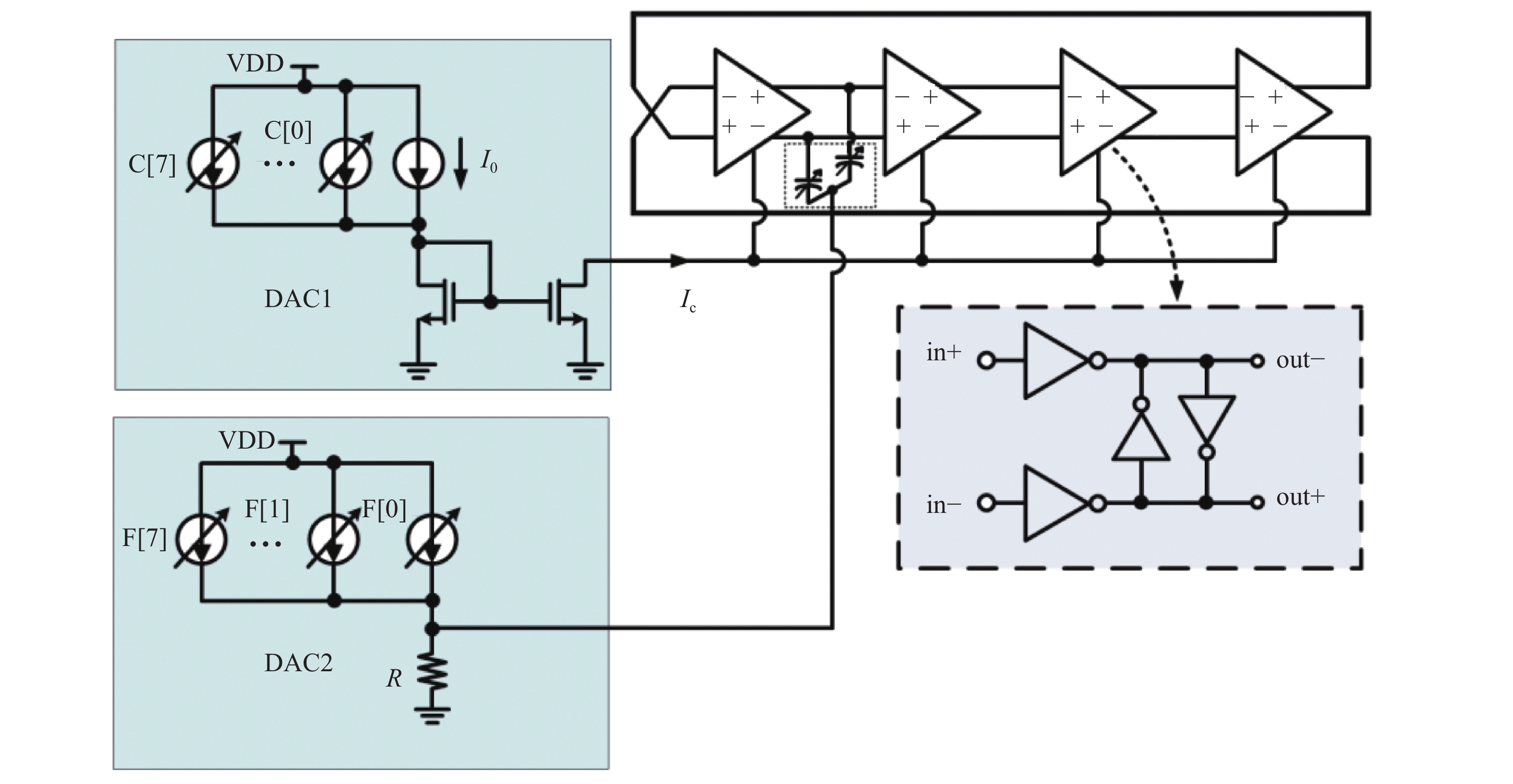
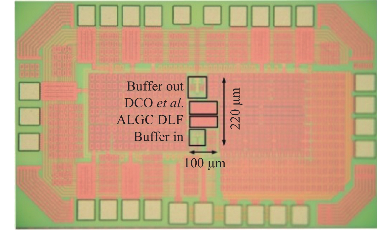
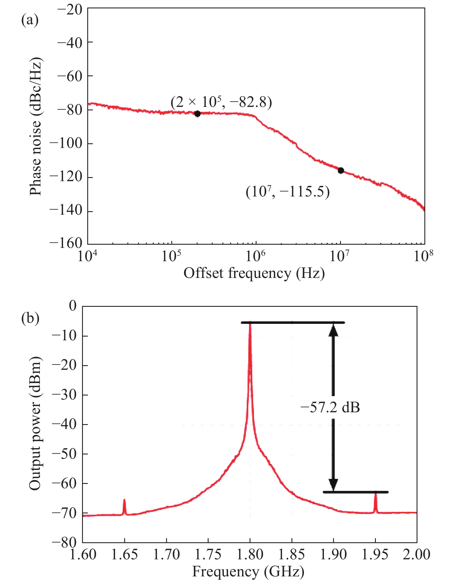
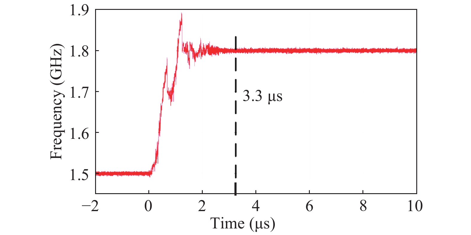
This paper proposes a fast-locking bang-bang phase-locked loop (BBPLL). A novel adaptive loop gain controller (ALGC) is proposed to increase the locking speed of the BBPLL. A novel bang-bang phase/frequency detector (BBPFD) with adaptive-mode-selective circuits is proposed to select the locking mode of the BBPLL during the locking process. Based on the detected results of the BBPFD, the ALGC can dynamically adjust the overall gain of the loop for fast-locking procedure. Compared with the conventional BBPFD, only a few gates are added in the proposed BBPFD. Therefore, the proposed BBPFD with adaptive-mode-selective circuits is realized with little area and power penalties. The fast-locking BBPLL is implemented in a 65 nm CMOS technology. The core area of the BBPLL is 0.022 mm2. Measured results show that the BBPLL operates at a frequency range from 0.6 to 2.4 GHz. When operating at 1.8 GHz, the power consumption is 3.1 mW with a 0.9-V supply voltage. With the proposed techniques, the BBPLL achieves a normalized locked time of 1.1 μs @ 100 MHz frequency jump. The figure-of-merit of the fast-locking BBPLL is −334 dB.


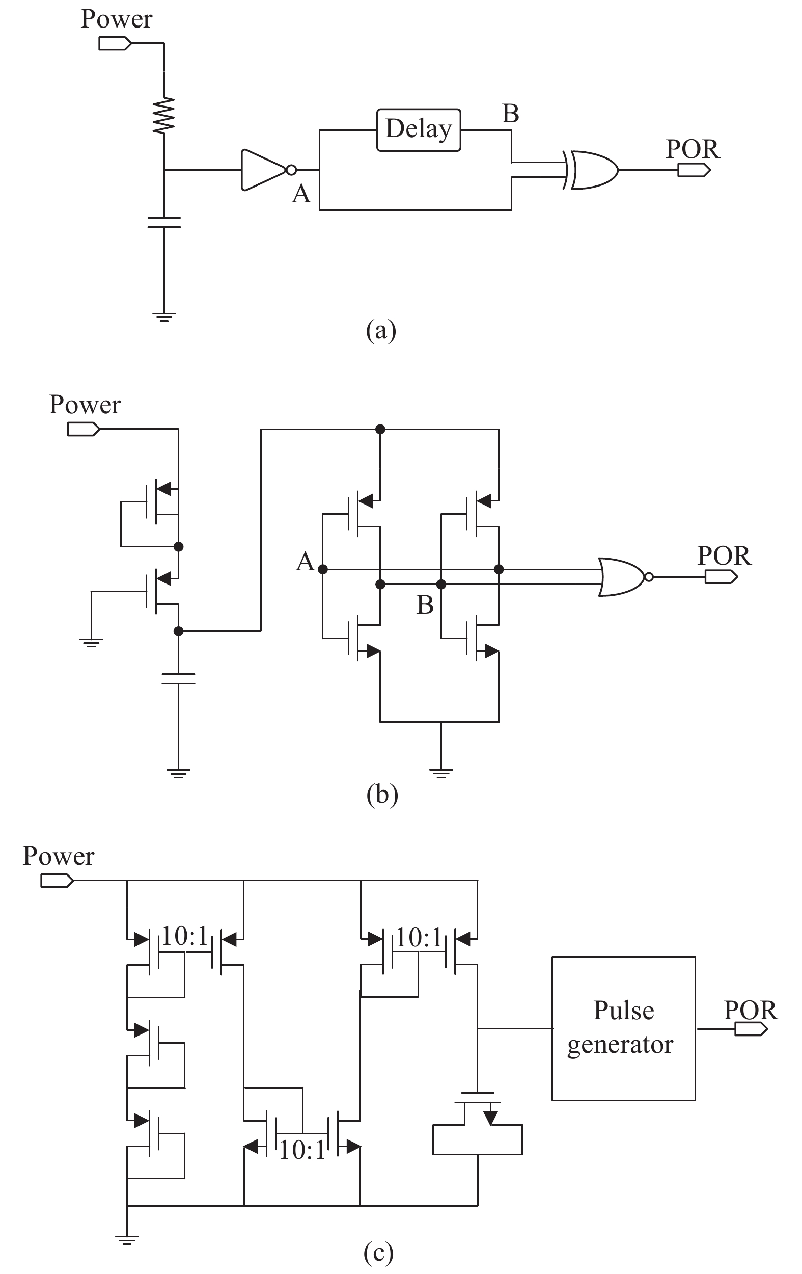
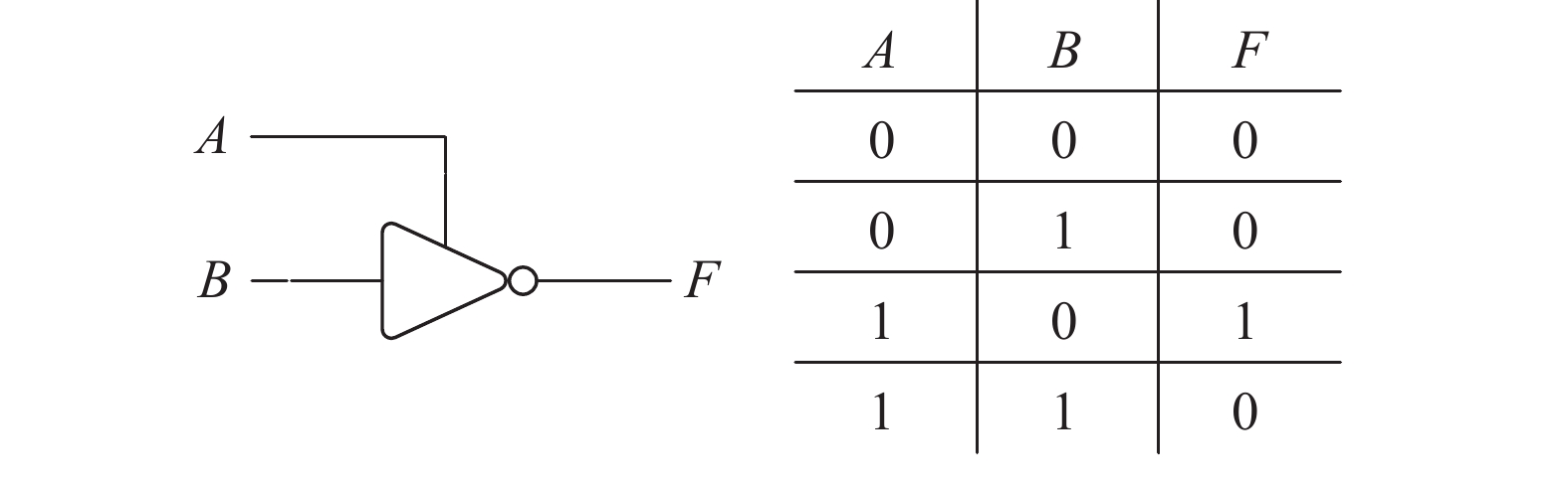
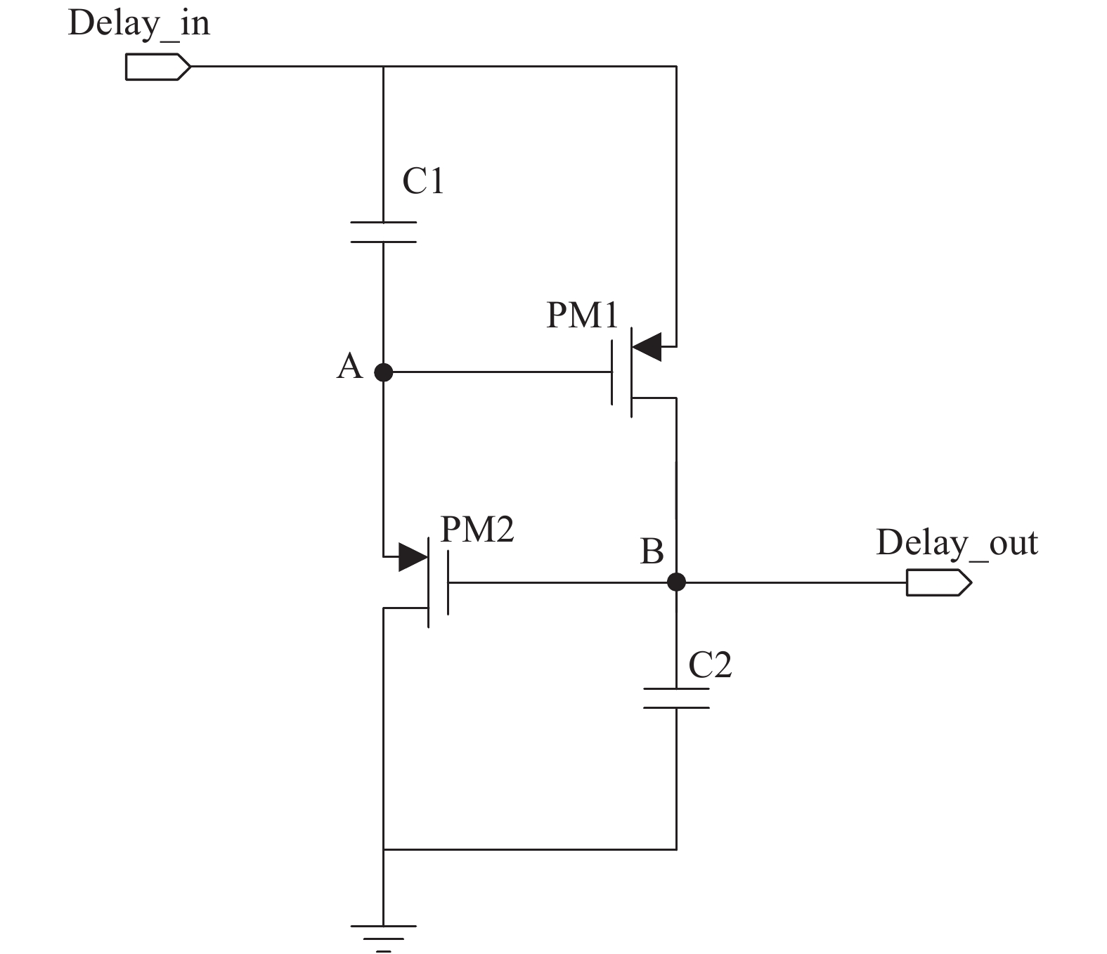
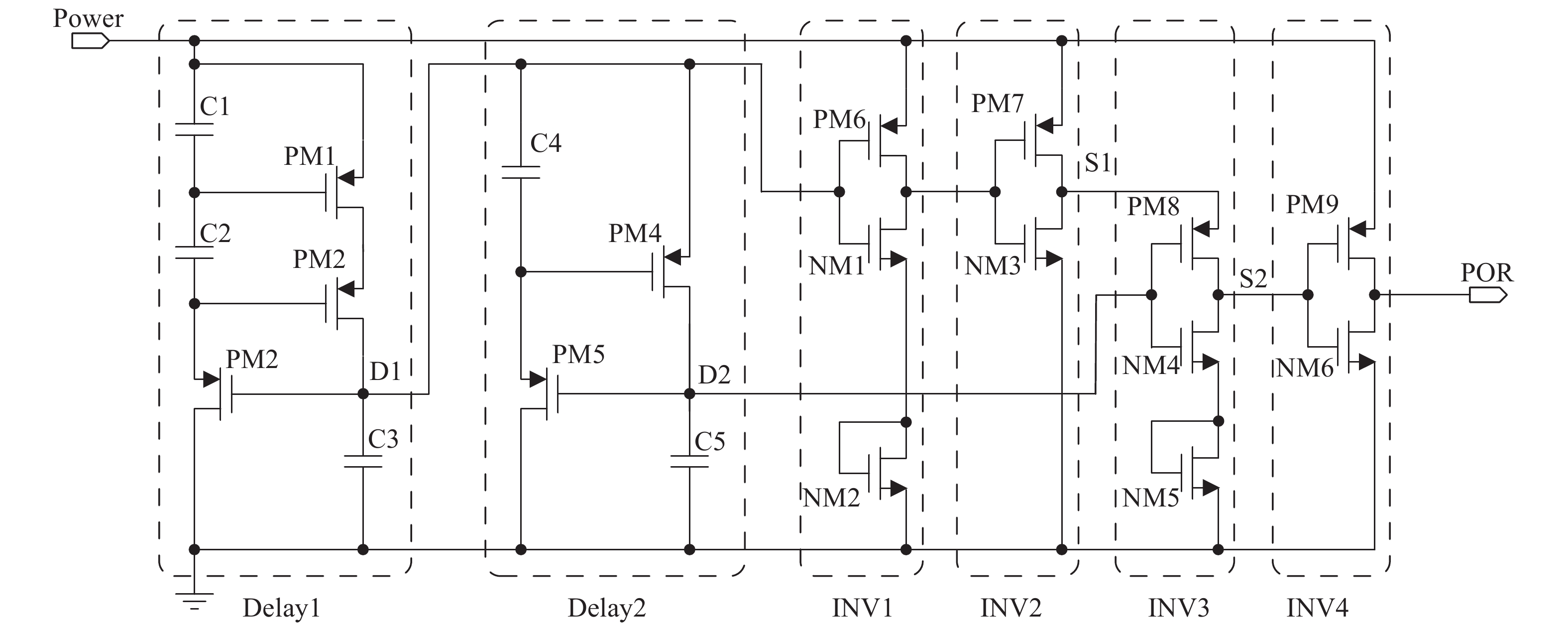
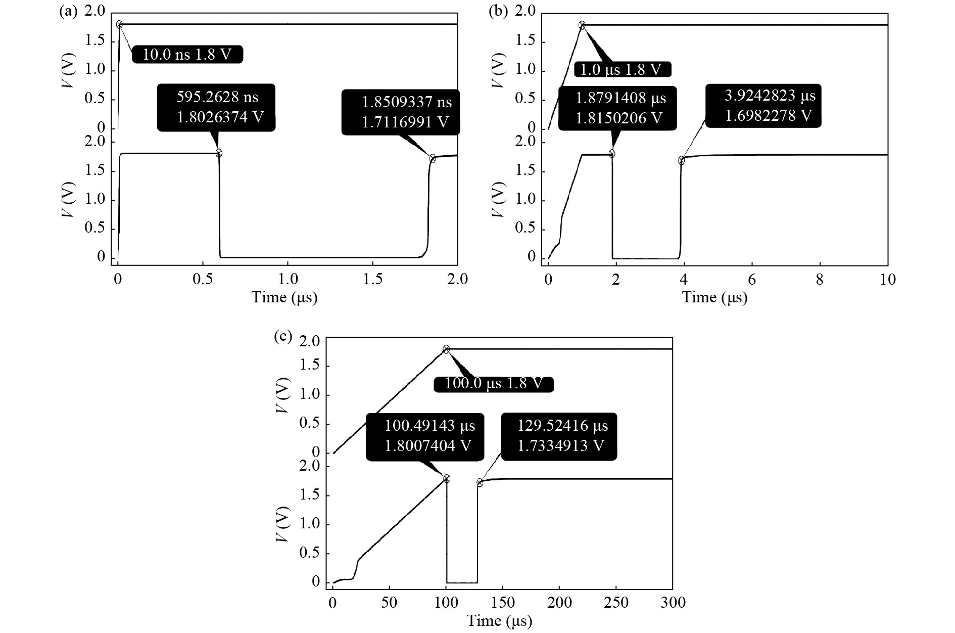
A novel power-on-reset (POR) circuit with simple architecture, small values of capacitances, ultra-lower power consumption, and self-adjustable delay time of reset pulse for passive UHF RFID tags is presented in this paper. A proposed delay element was adopted for the features of small capacitances and wide power supply rise time range. An inverter was used as a two-inputs logic device to simplify the architecture of the circuit. The technology used for design and simulation is SMIC 0.18 μm RF. Simulation results show that the circuit functions well under different process corners with different power supply rise time, and is able to generate a POR signal after the power supply is briefly powered off. The static power consumption is less than 30 pA. Moreover, the circuit operates properly along with other modules of analog front-end.


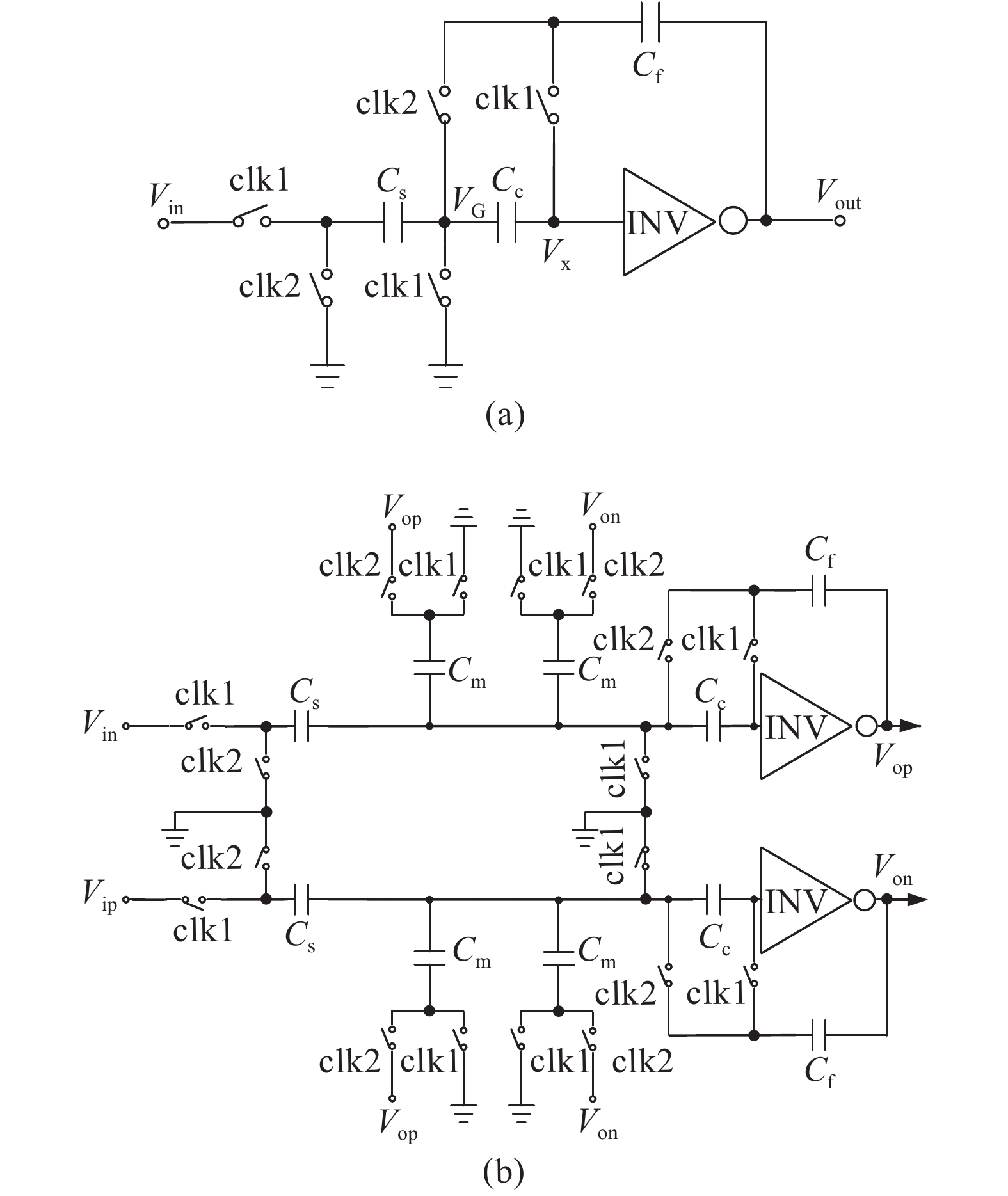
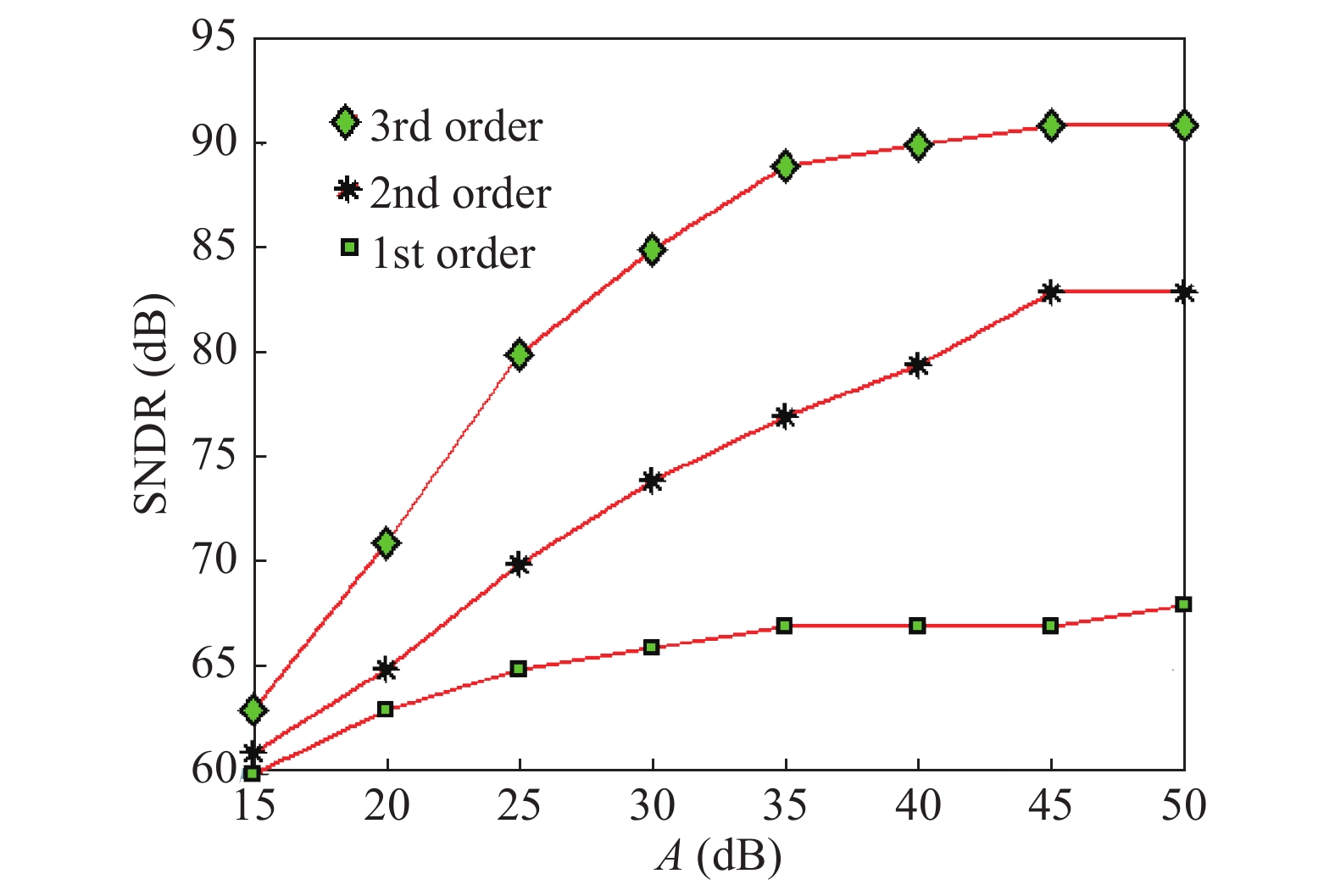
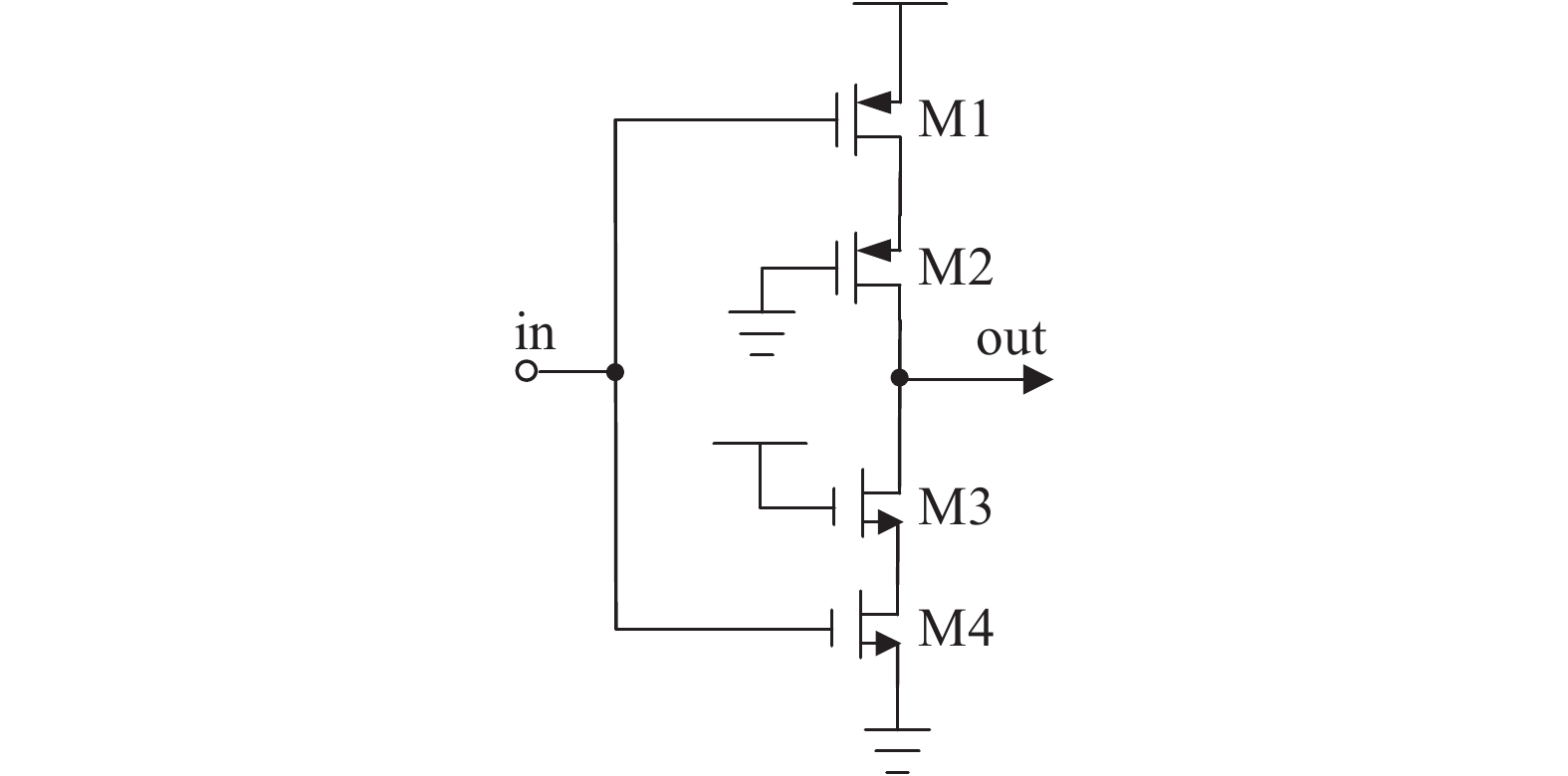
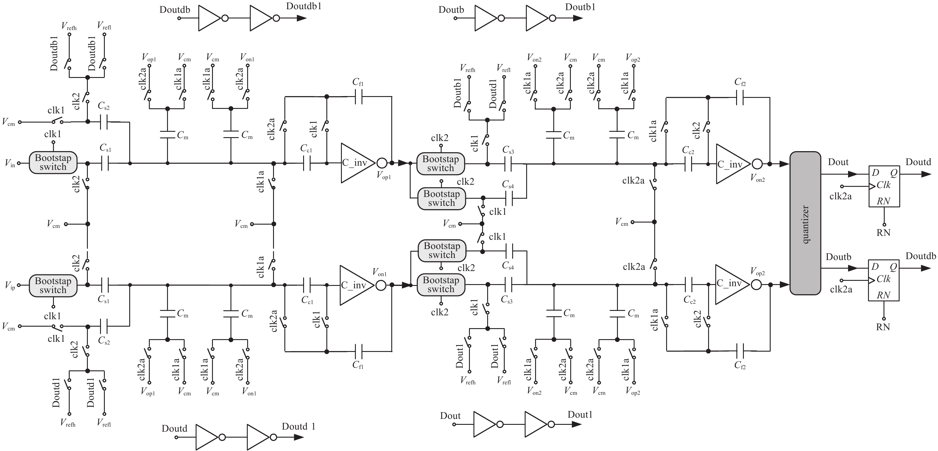
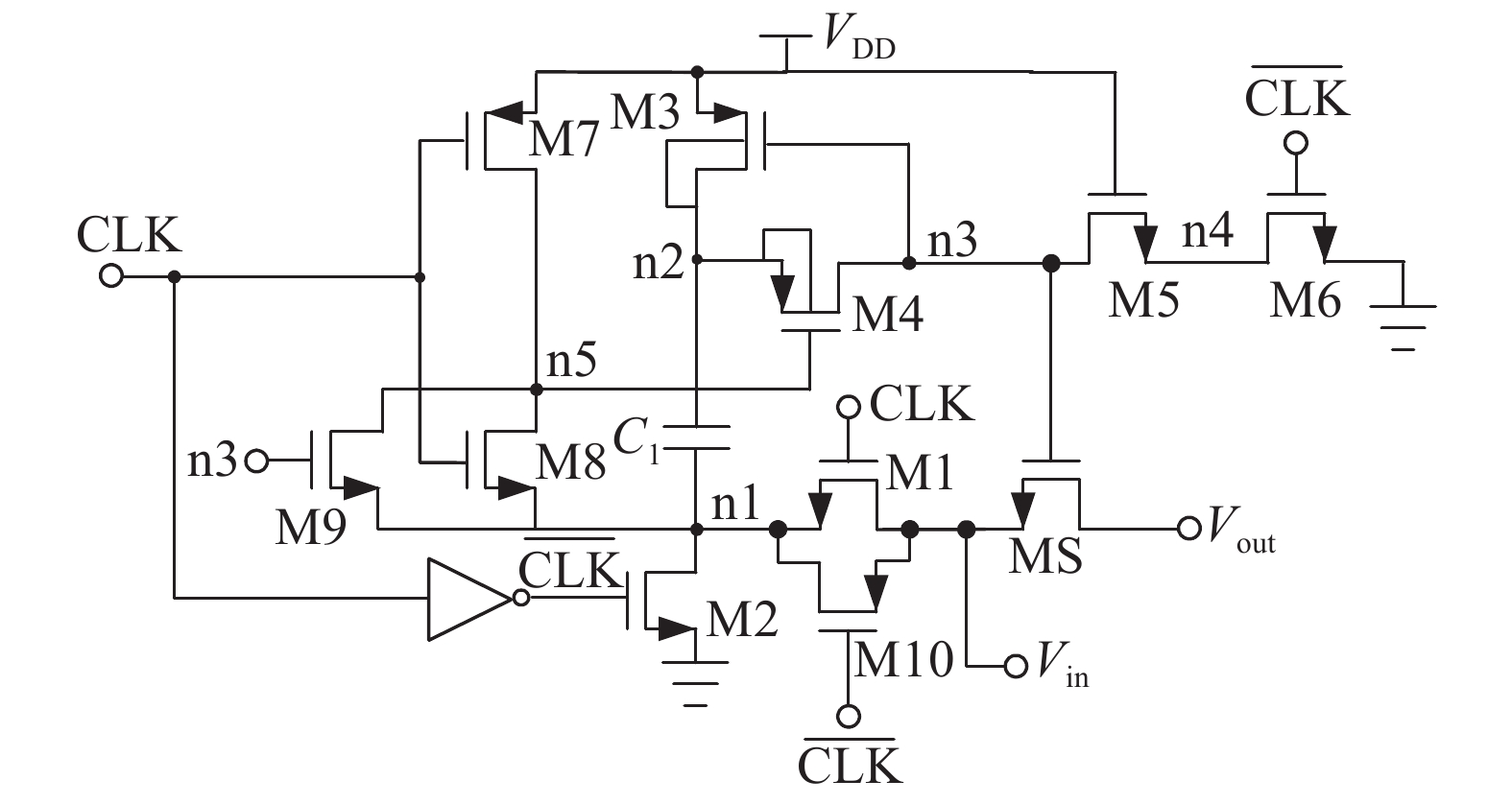
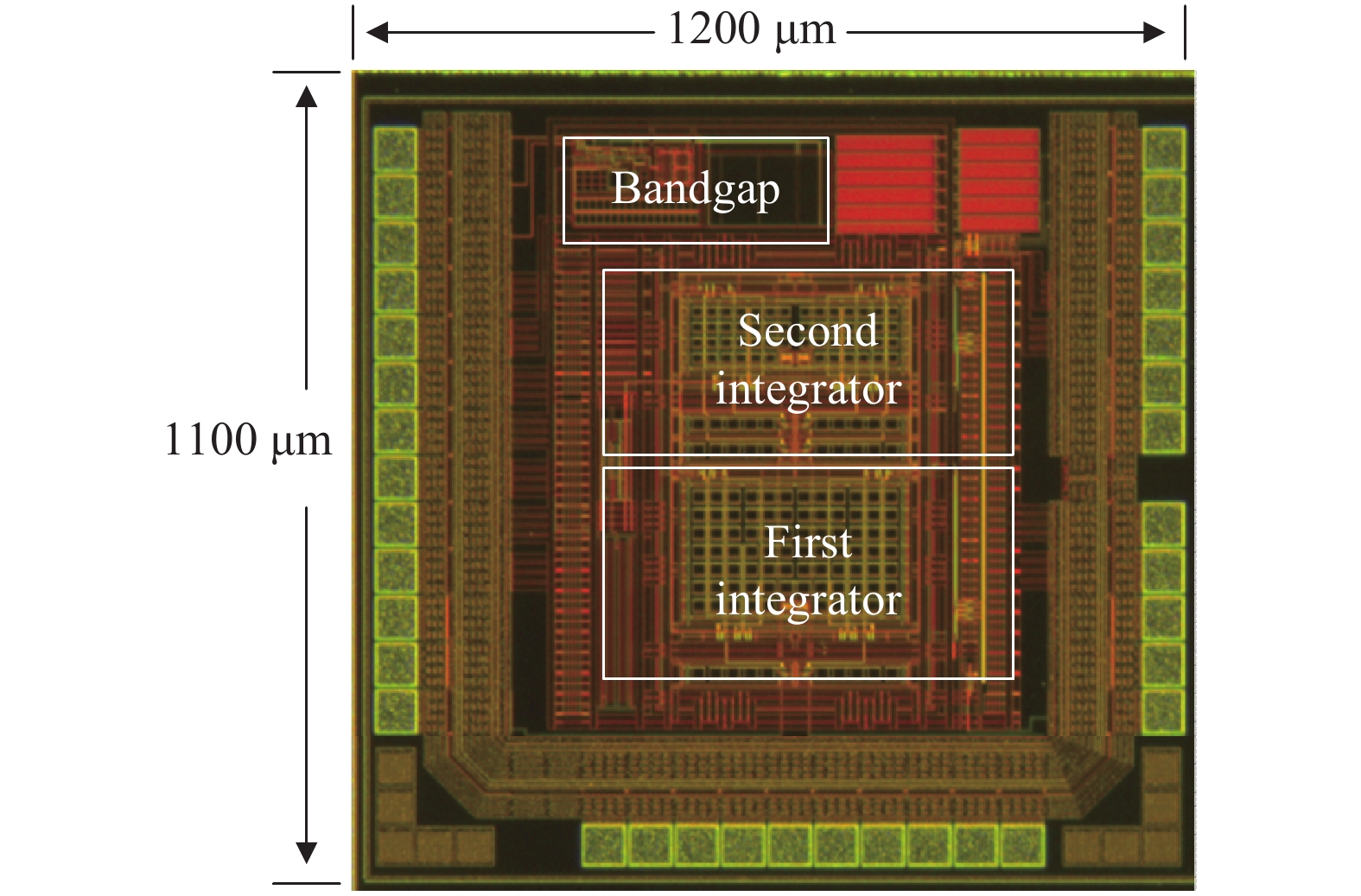
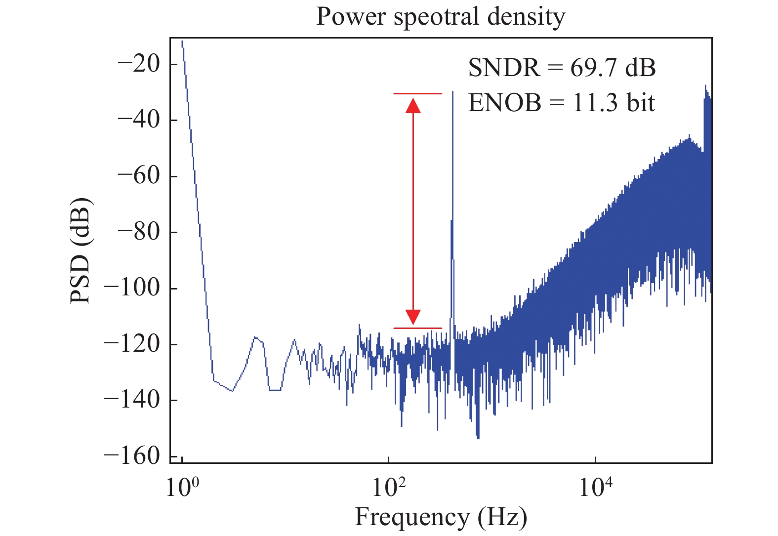
In this paper a 0.6 V, 14 bit/500 Hz subthreshold inverter-based sigma–delta modulator is proposed. In the first integrator of the modulator, a bootstrap switch is used to accomplish accurate signal sampling. Without a transconductor operational amplifier (OTA), the sigma–delta modulator adopts a cascode inverter in the subthreshold region to save power consumption. The modulator is fabricated with a 0.13 μm CMOS mixed-signal process. The experiment results show that with the 0.6 V power supply it achieves a maximum SNDR of 69.7 dB and an ENOB of 11.3 bit, respectively, but only consumes 5.07 μw power dissipation.


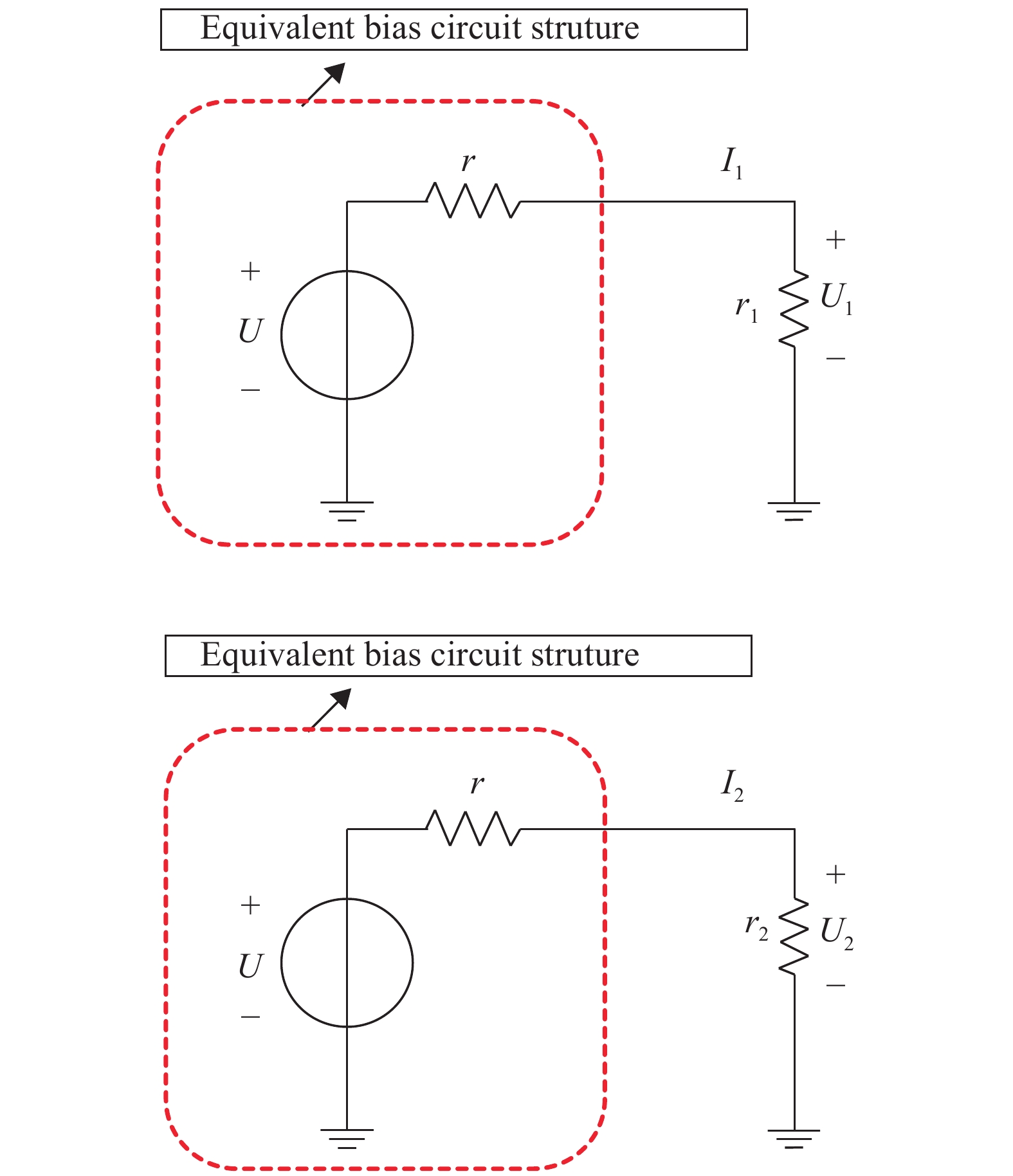
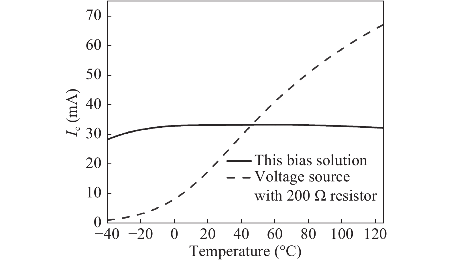
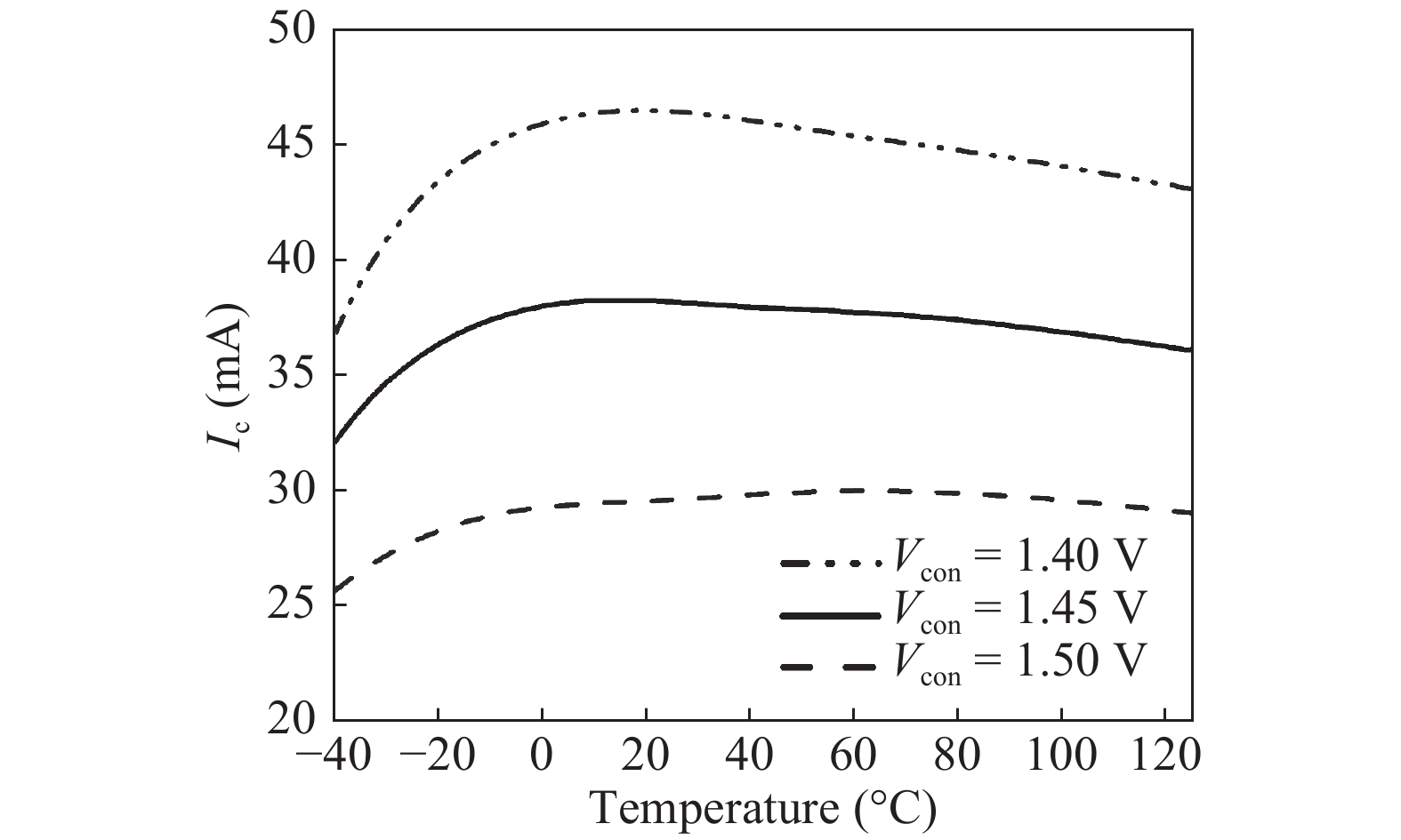
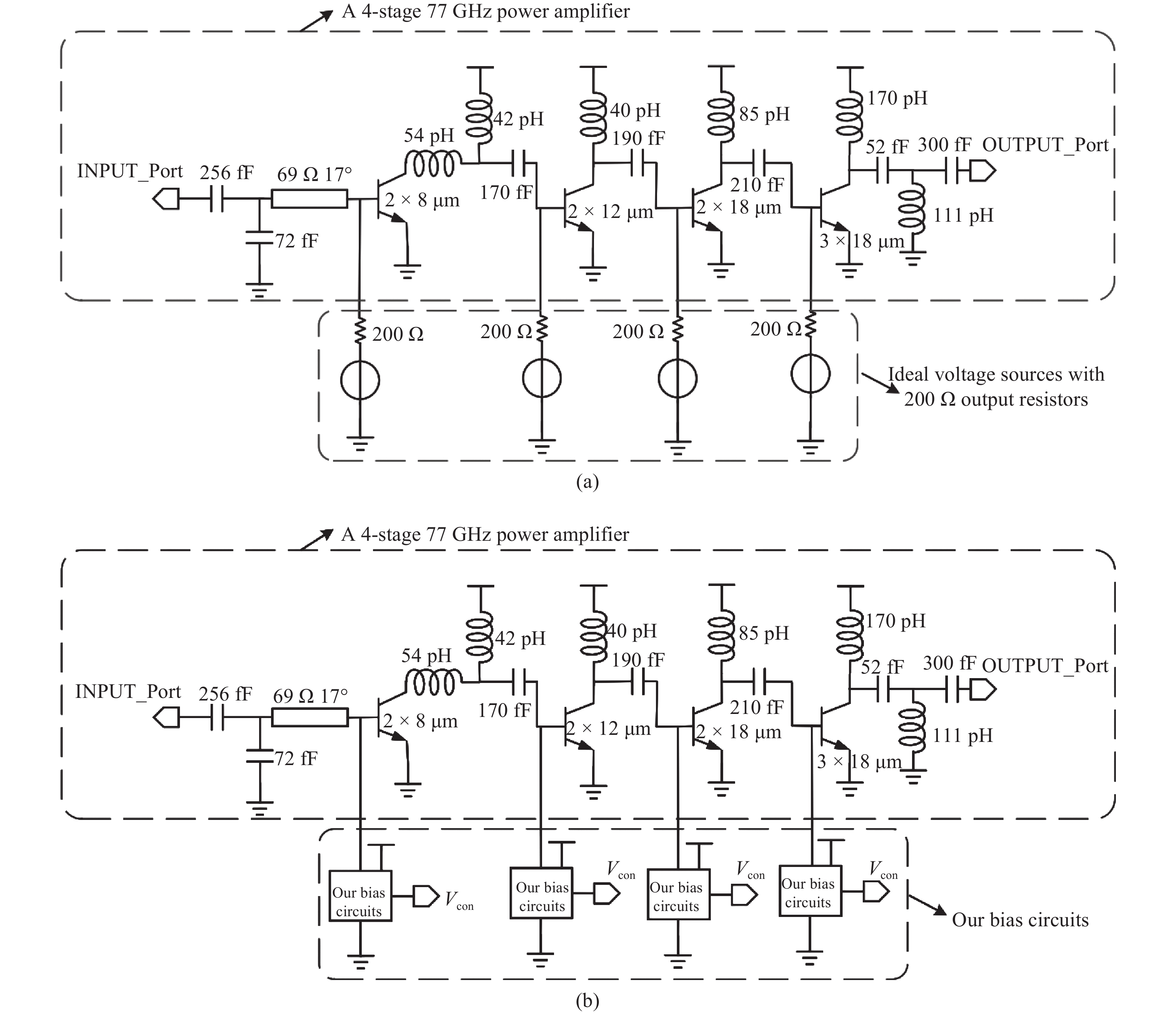
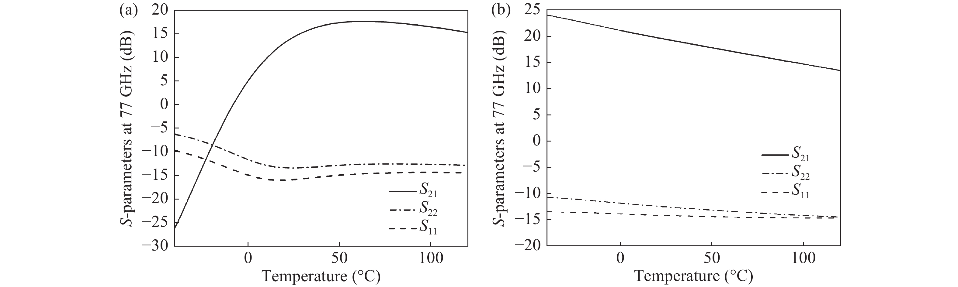
The performance of the power amplifier determines the detection capability of 77 GHz automotive radar, and the bias circuit is one of the most important parts of a silicon-germanium power amplifier. In this paper, we discussed and designed an on-chip bias circuit based on a silicon-germanium heterojunction bipolar transistor, which is used for the W-band silicon–germanium power amplifier. Considering the low breakdown voltage and the correlation between characteristic frequency and bias current density of the silicon-germanium heterojunction bipolar transistor, the bias circuit is designed to improve the breakdown voltage of the power amplifier and meet the W band characteristic frequency at the same time. The simulation results show that the designed bias circuit can make the amplifier operate normally from −40 to 125 °C. In addition, the output power and smooth controllability of the power amplifier can be adjusted by controlling the bias circuit.


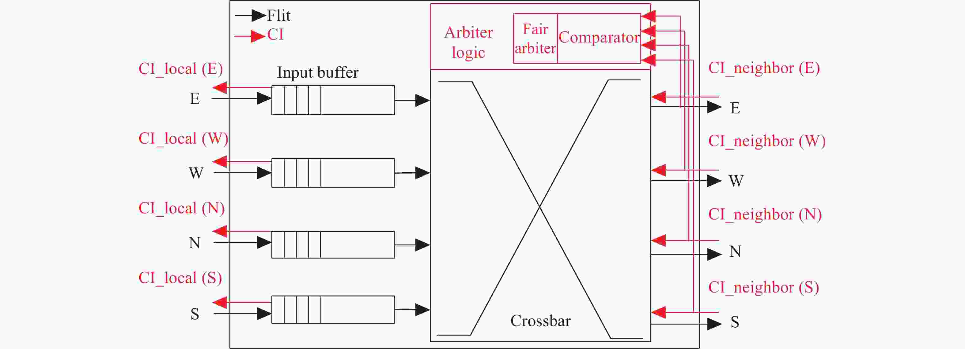
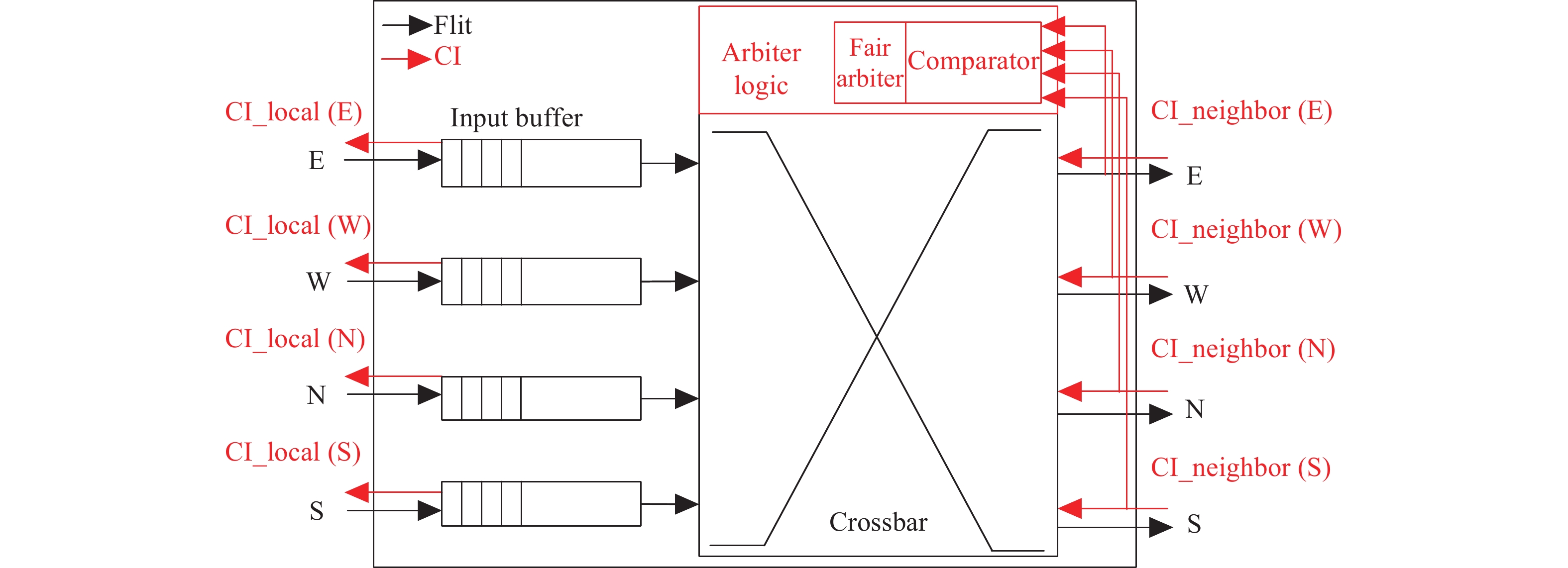
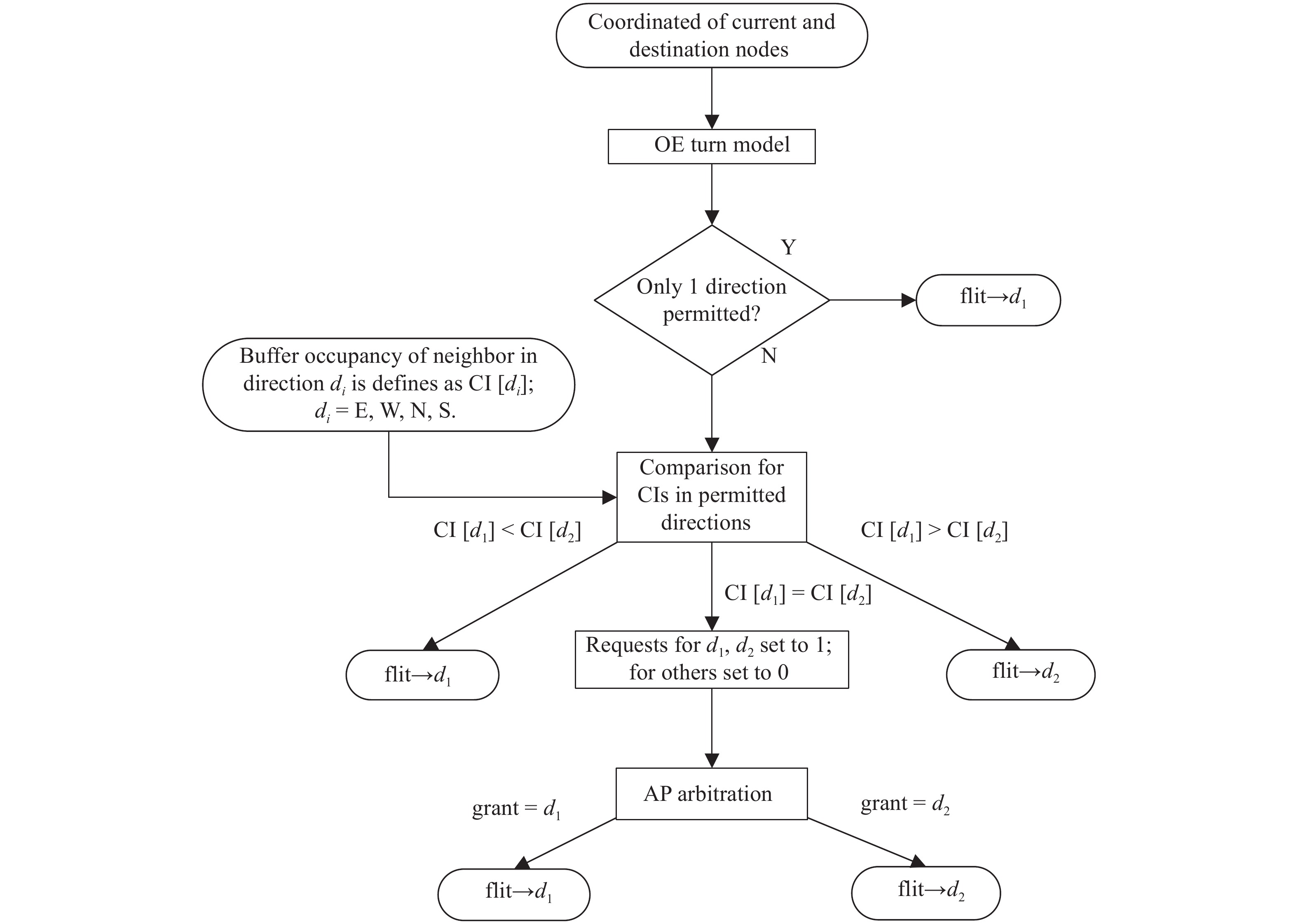
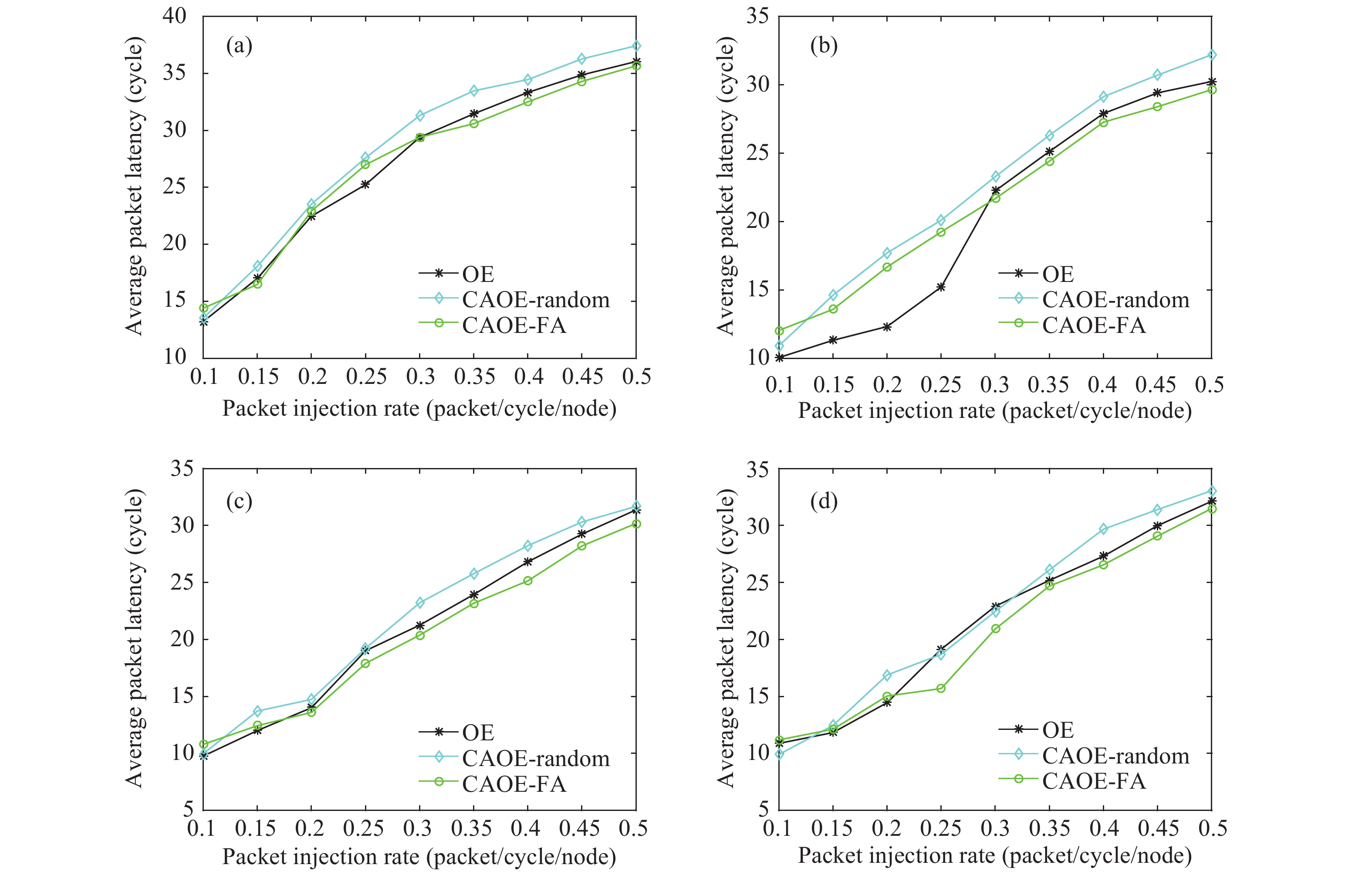
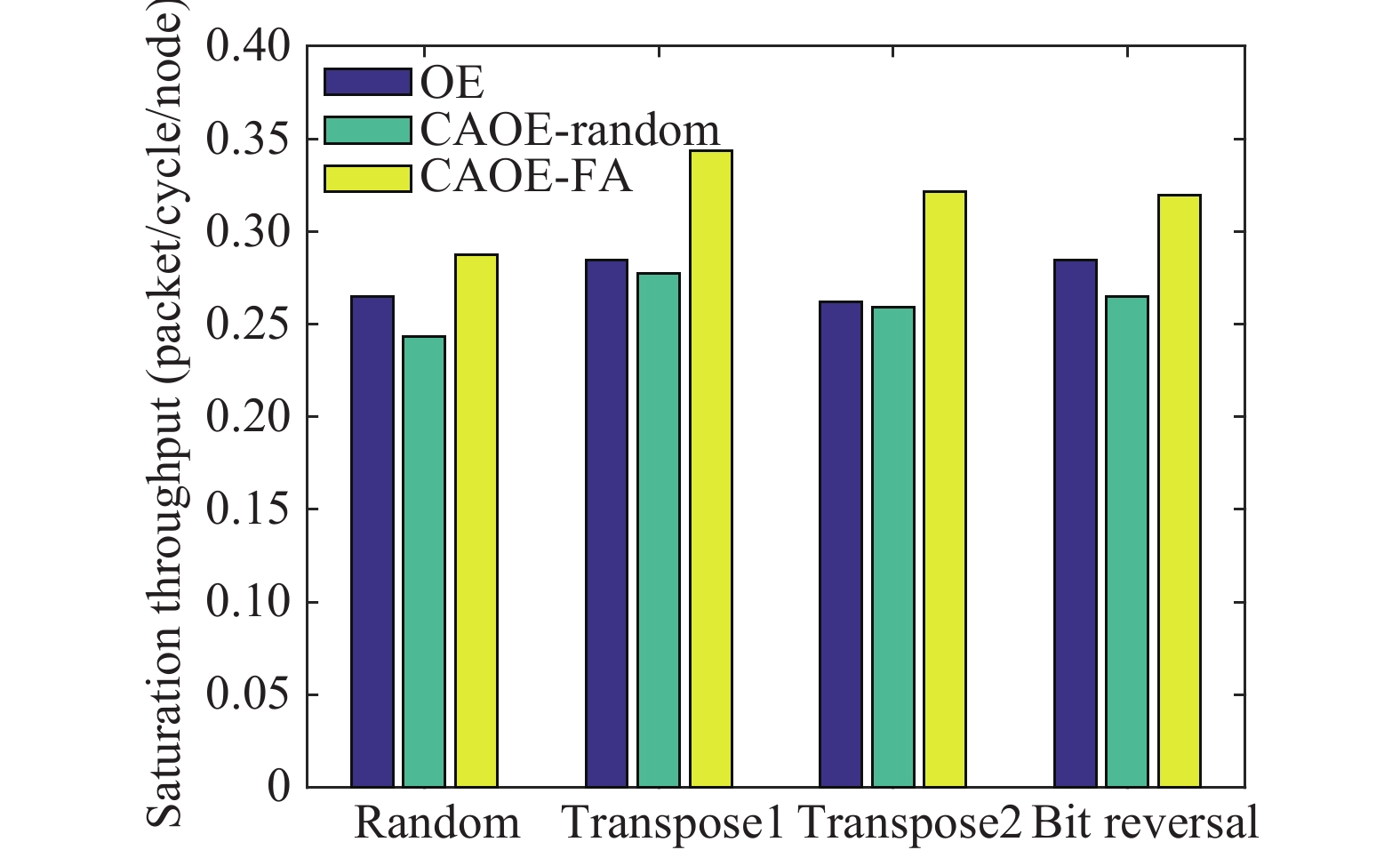
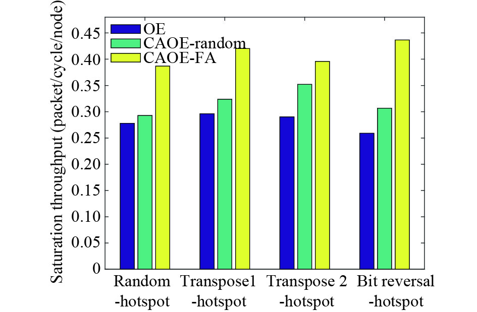
To meet the demand for high on-chip network performance, flexible routing algorithms supplying path diversity and congestion alleviation are required. We propose a CAOE-FA router as a combination of congestion-awareness and fair arbitration. Buffer occupancies from downstream neighbors are collected to indicate the congestion levels, among the candidate outputs permitted by the odd-even (OE) turn model, the lightest loaded direction is selected; fair arbitration is employed for the condition of the same congestion level to replace random selection. Experimental results show that the CAOE-FA can reduce the average packet latency by up to 22.18% and improve the network throughput by up to 68.58%, with ignorable price of hardware cost.


Due to its low electrical loss and low process cost, a glass interposer has been developed to provide a compelling alternative to the silicon-based interposer for packaging of future 2-D and 3-D ICs. In this study, through glass vias (TGVs) are used to implement 3-D inductors for minimal footprint and large quality factor. Using the inductors and parallel plate capacitors, a compact 3-D Wilkinson power divider is designed and analyzed. Compared with some reported power dividers, the proposed TGV-based circuit has an ultra-compact size and excellent electrical performance.

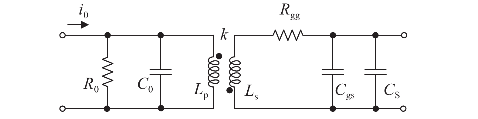
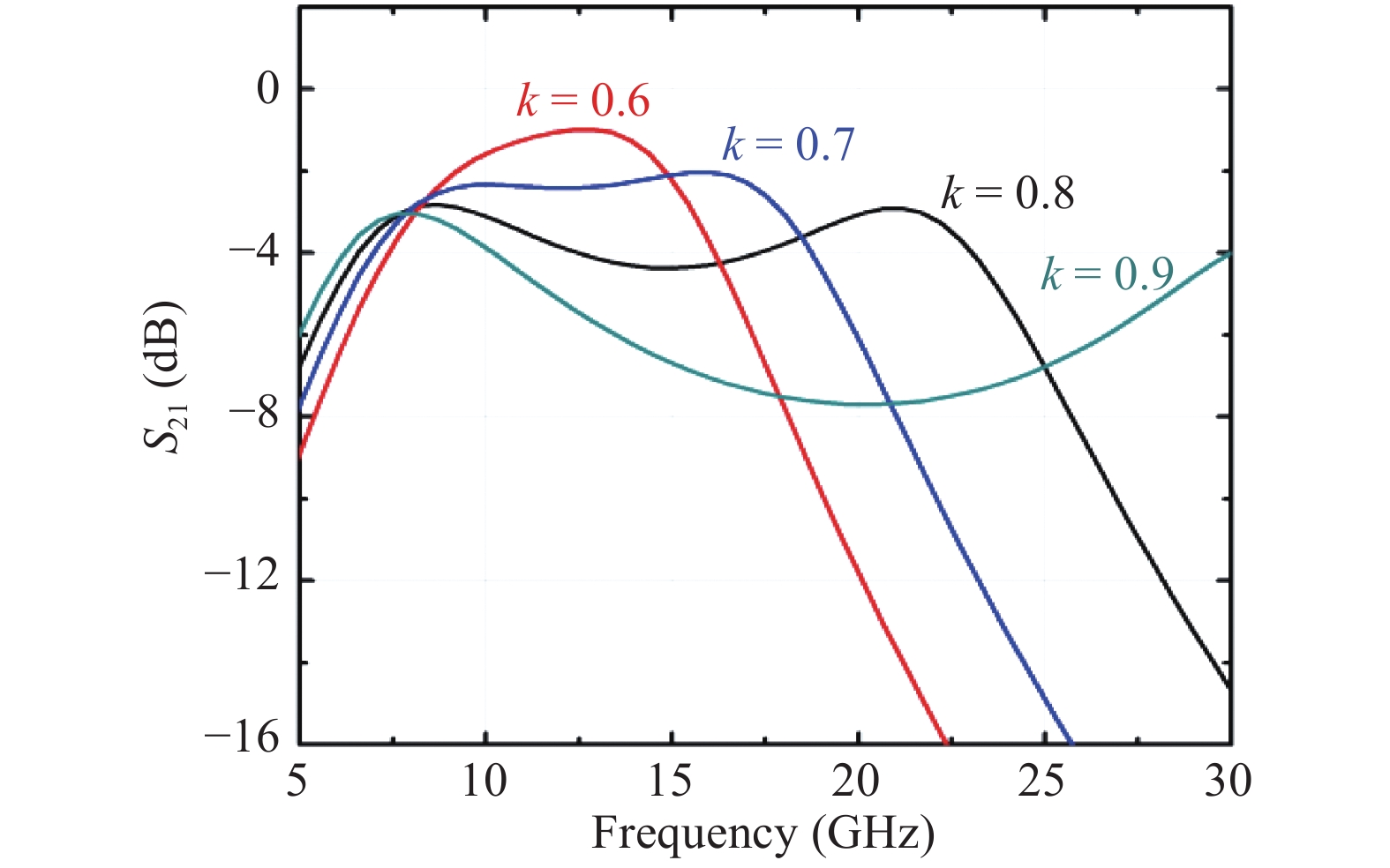
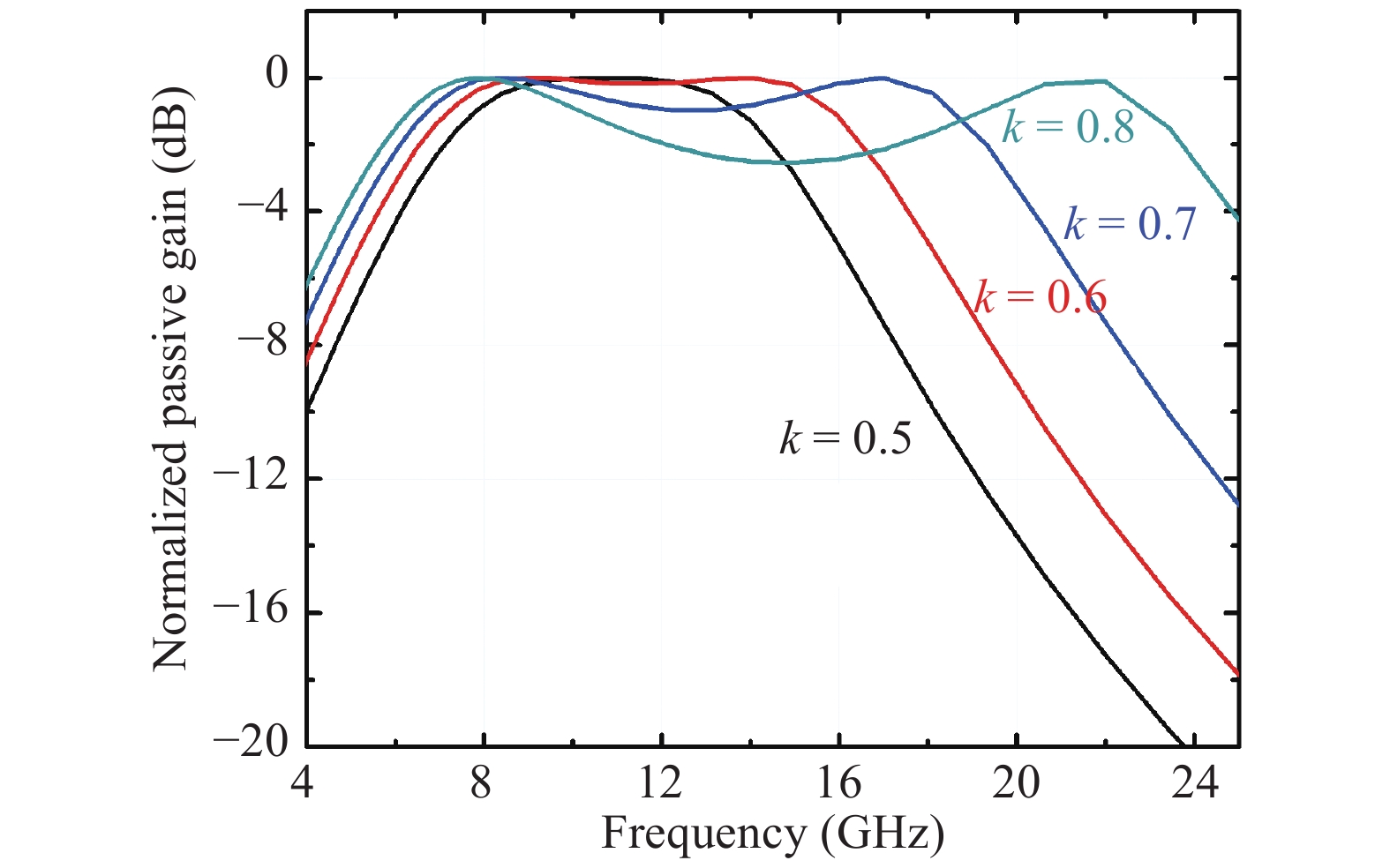
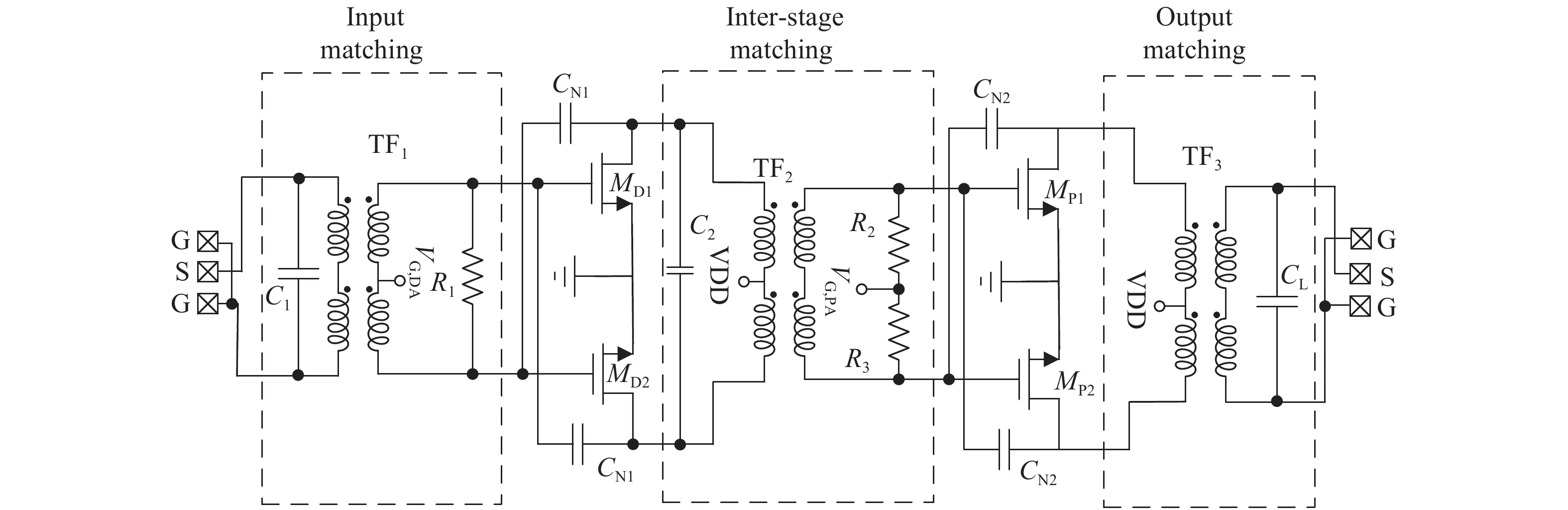
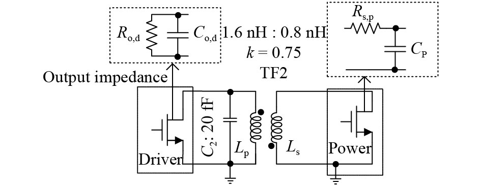
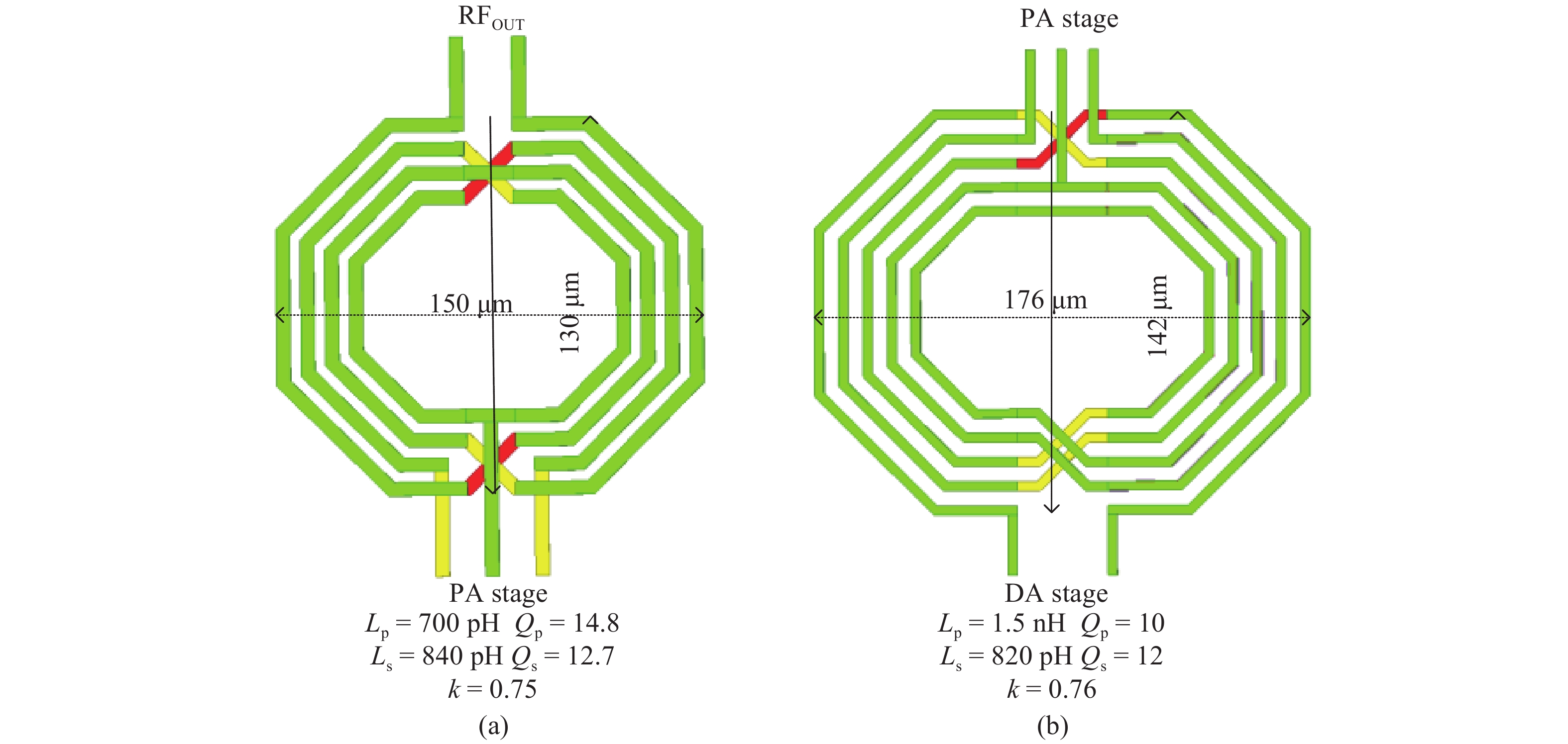
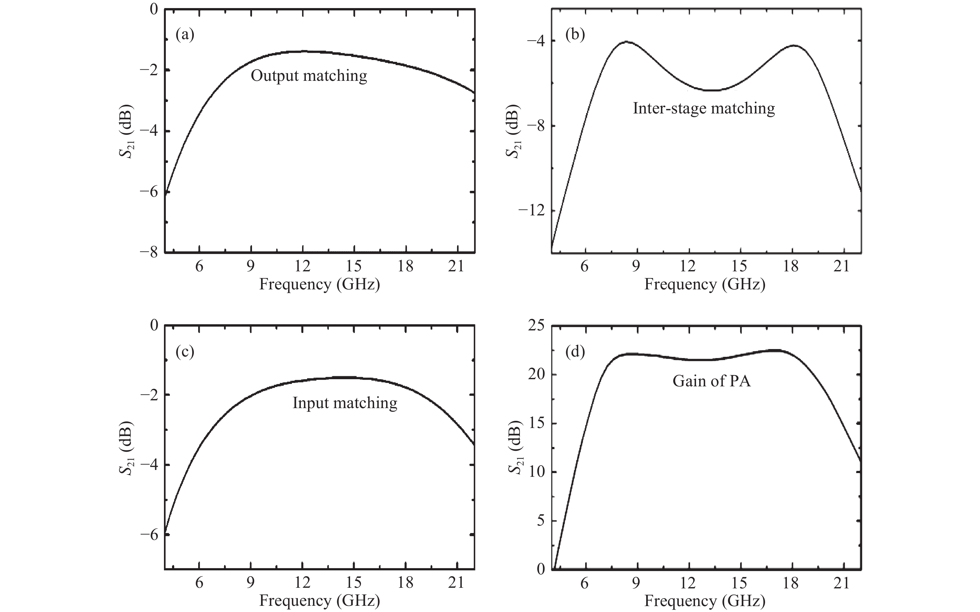
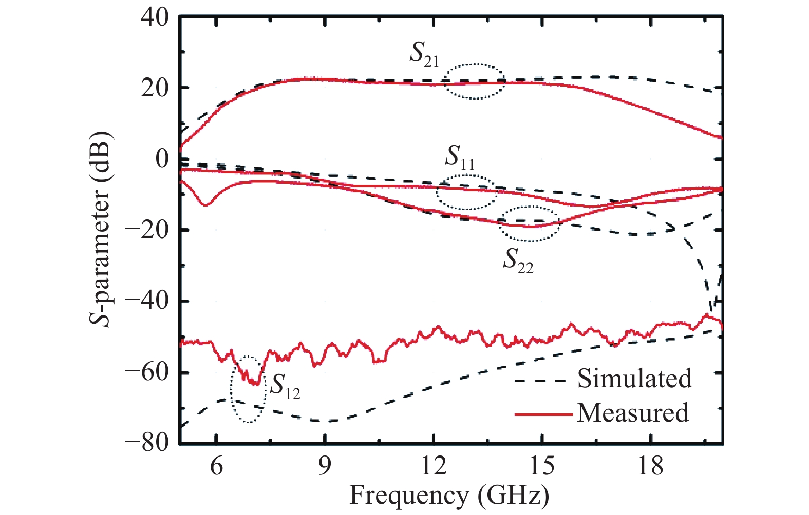
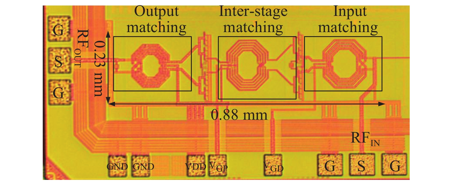
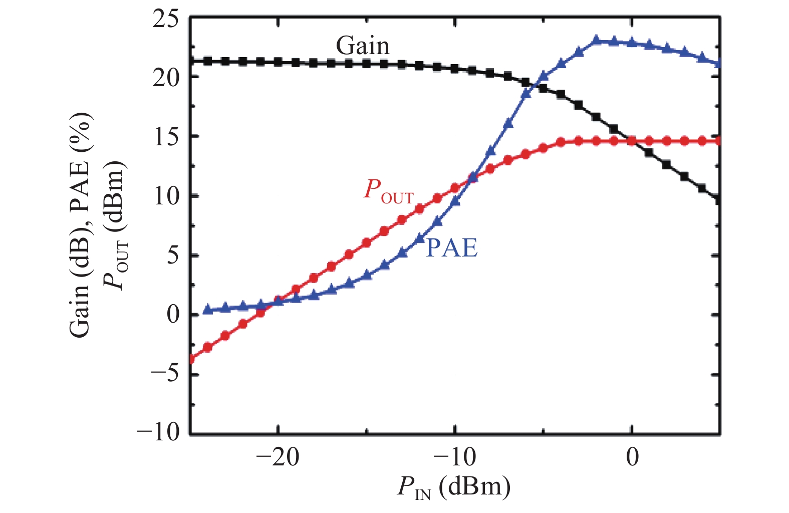
A wideband CMOS power amplifier with high gain and excellent gain flatness for X–Ku-band radar phased array is proposed in this paper. Excellent gain flatness is achieved with transformer based matching networks (TMNs), in which the gain fluctuation of an inter-stage matching network can be compensated by the proposed design methods. The circuit is fabricated in the TSMC 65 nm RF CMOS process. The proposed technique is verified by the measurement results, which show that the wideband PA achieves gain of 21–22.5 dB with only ±0.75 dB gain fluctuation and 13–14.6 dBm flat output power between 7.5 and 15.5 GHz, and a little more ripple in the rest of the X–Ku band due to the inaccuracy of passive modelling at high frequency. The circuit delivers saturated and 1 dB-compressed output power of 14.6 and 11.3 dBm respectively at 13 GHz, for a maximal power-added efficiency (PAE) of 23%.


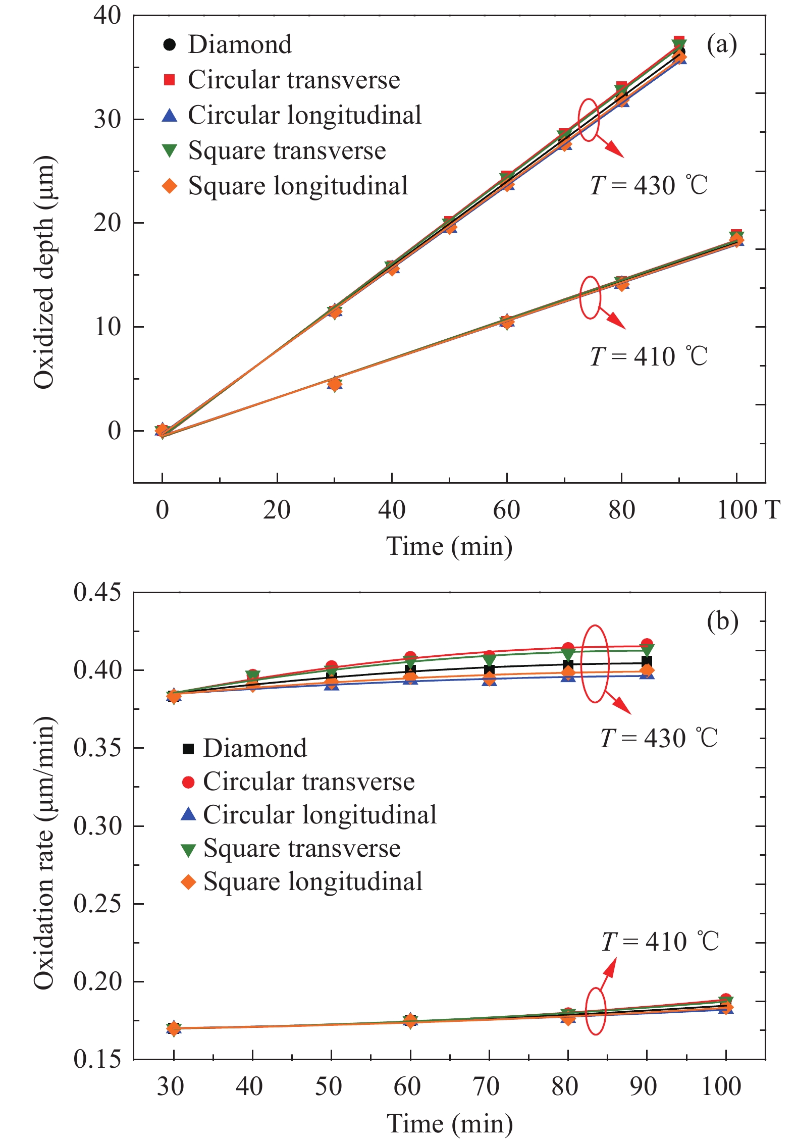
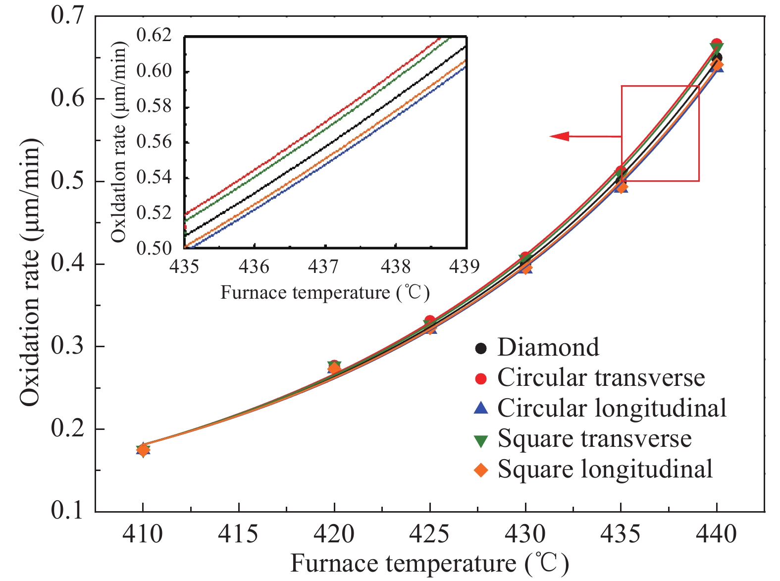
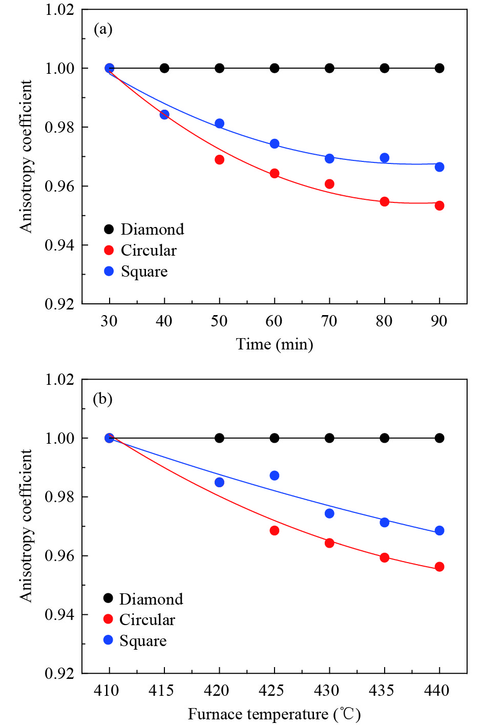
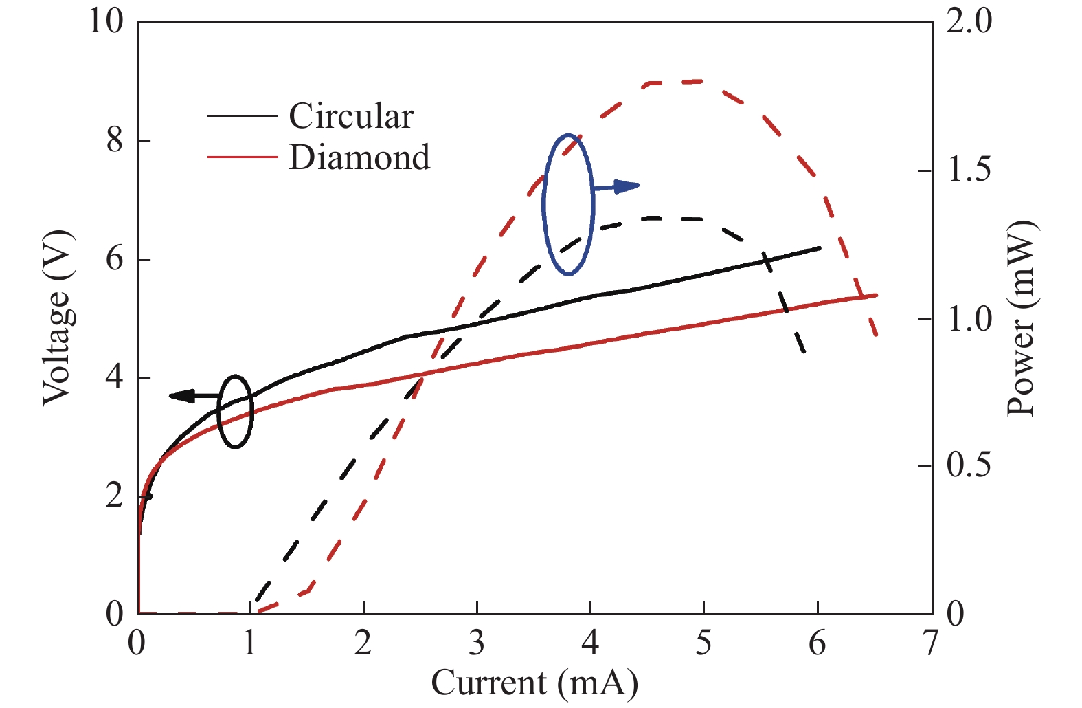
Vertical cavity surface emitting lasers (VCSELs) are widely used in optical communications and optical interconnects due to their advantages of low threshold, low power consumption and so on. Wet nitrogen oxidation technology, which utilizes H2O molecules to oxidize the Al0.98Ga0.02As, is used for electrical and optical mode confinement. In this paper, the effects of oxidation time, oxidation temperature and oxidation anisotropy on the oxidation rate are explored and demonstrated. The ratio of oxidation rate on [0–11] to [011] crystal orientation is defined as oxidation anisotropy coefficient, which decreases with the increase of oxidation temperature and oxidation time. In order to analyze the effect of the oxidation anisotropy on the VCSEL performance, an oxide-aperture of the VCSELs with two difference shapes is designed and then fabricated. The static performance of these fabricated VCSELs has been measured, whose threshold current ratio ~ 0.714 is a good agreement with that of the theoretical calculation value ~ 0.785. Our research on wet nitrogen oxidation and its anisotropy serves as an important reference in the batch fabrication of large-area VCSELs.
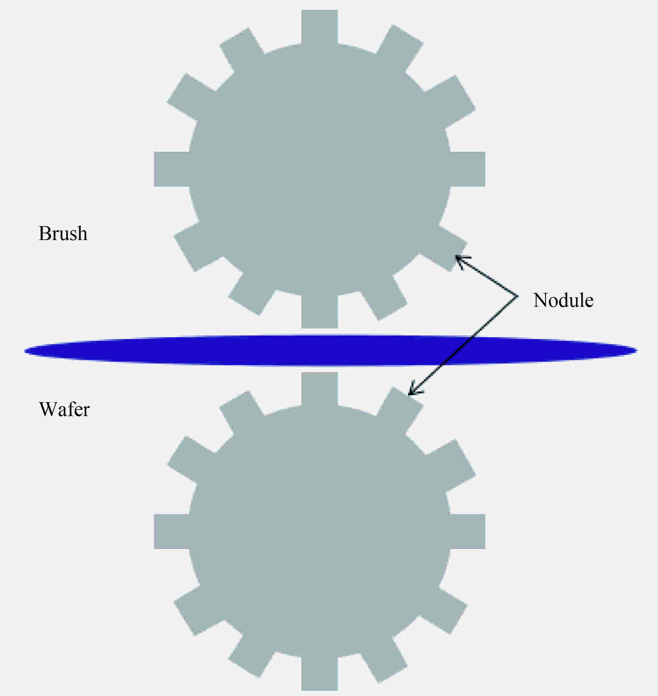
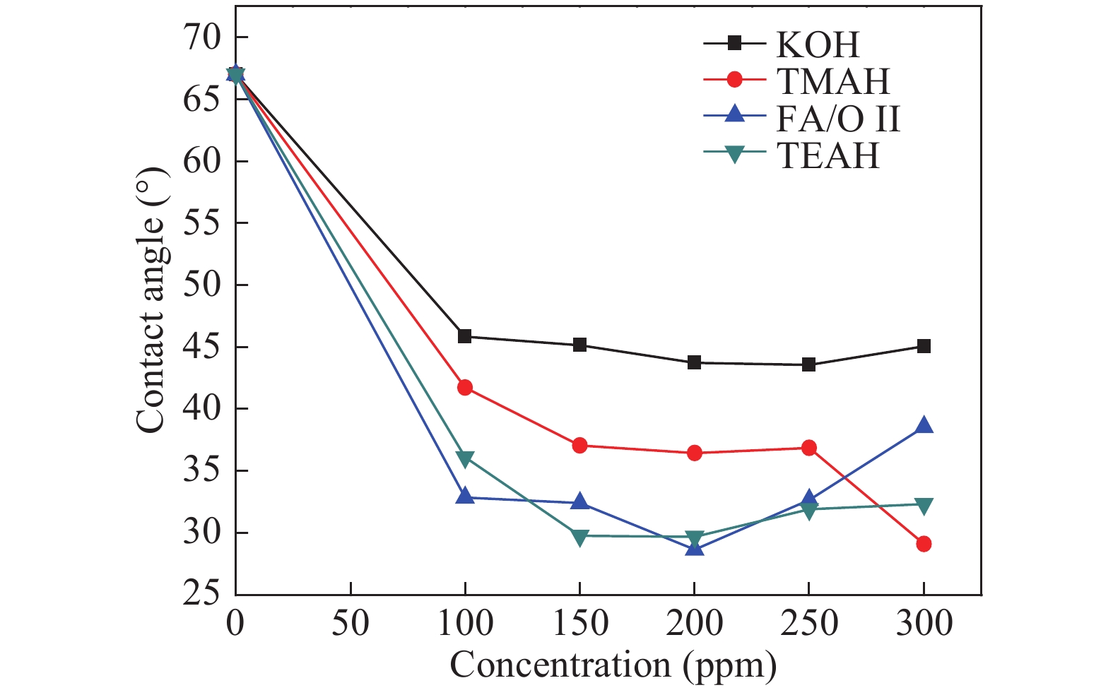
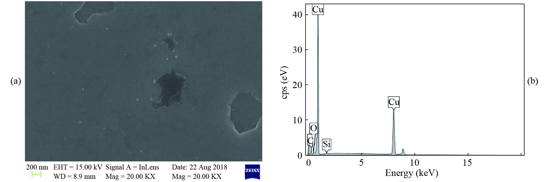
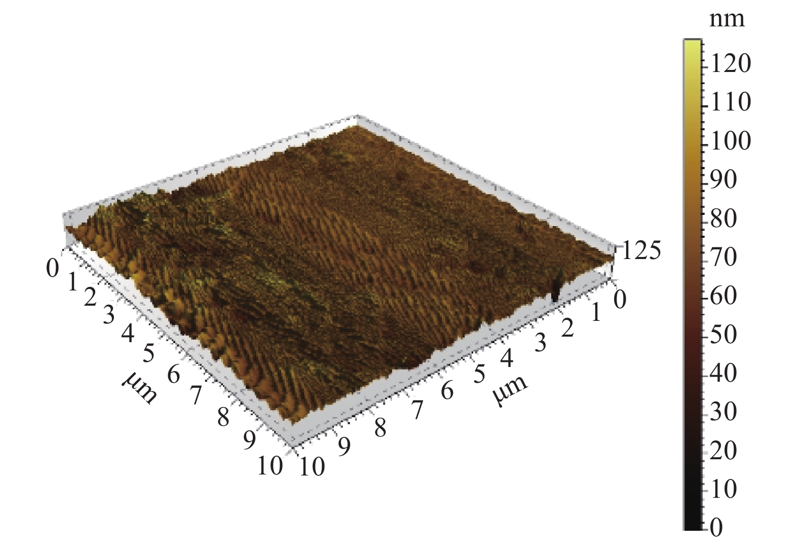
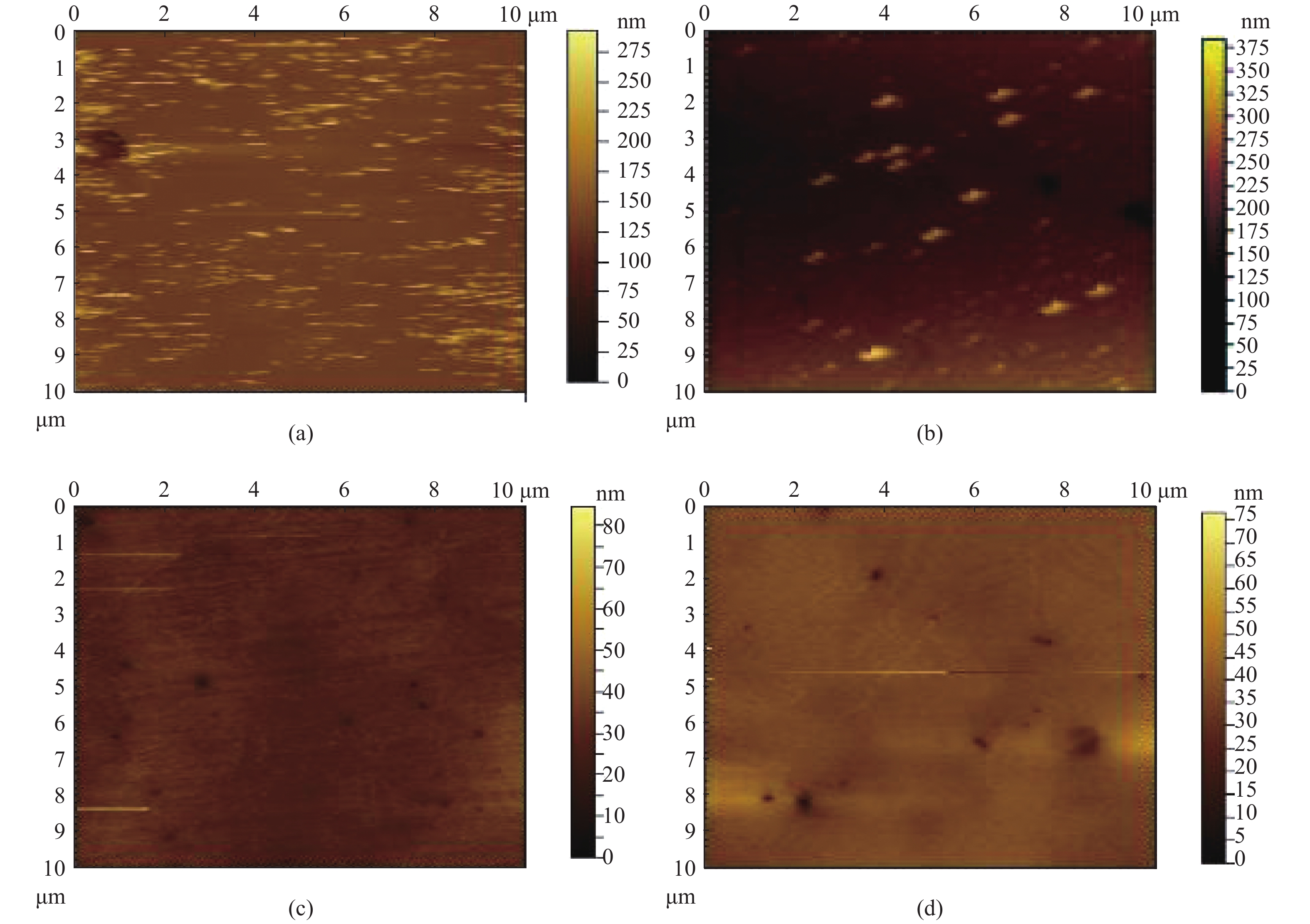
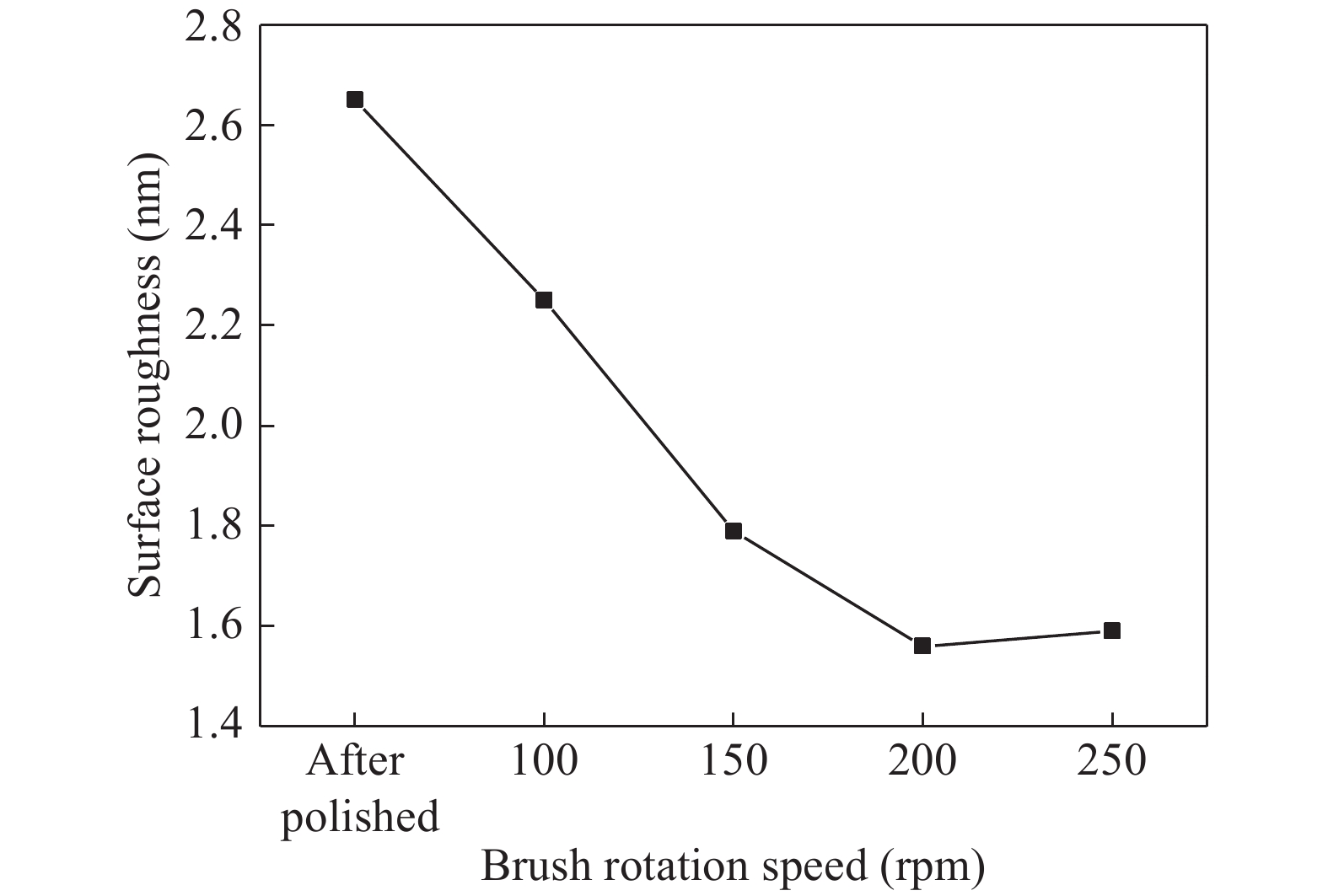
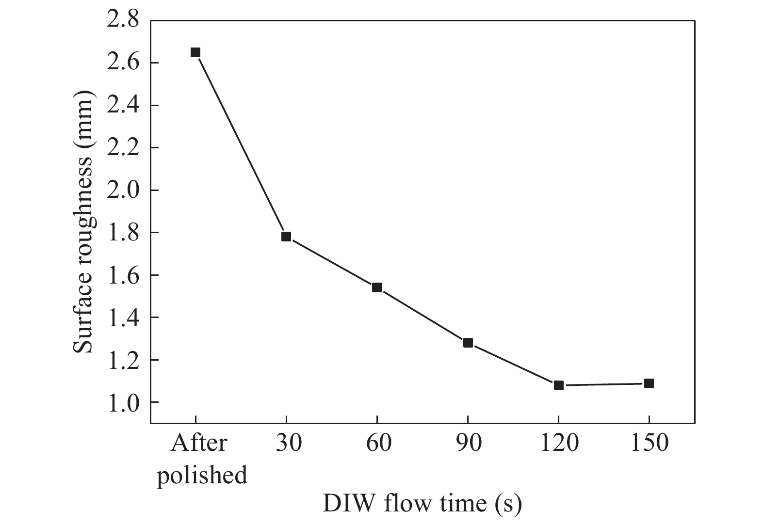
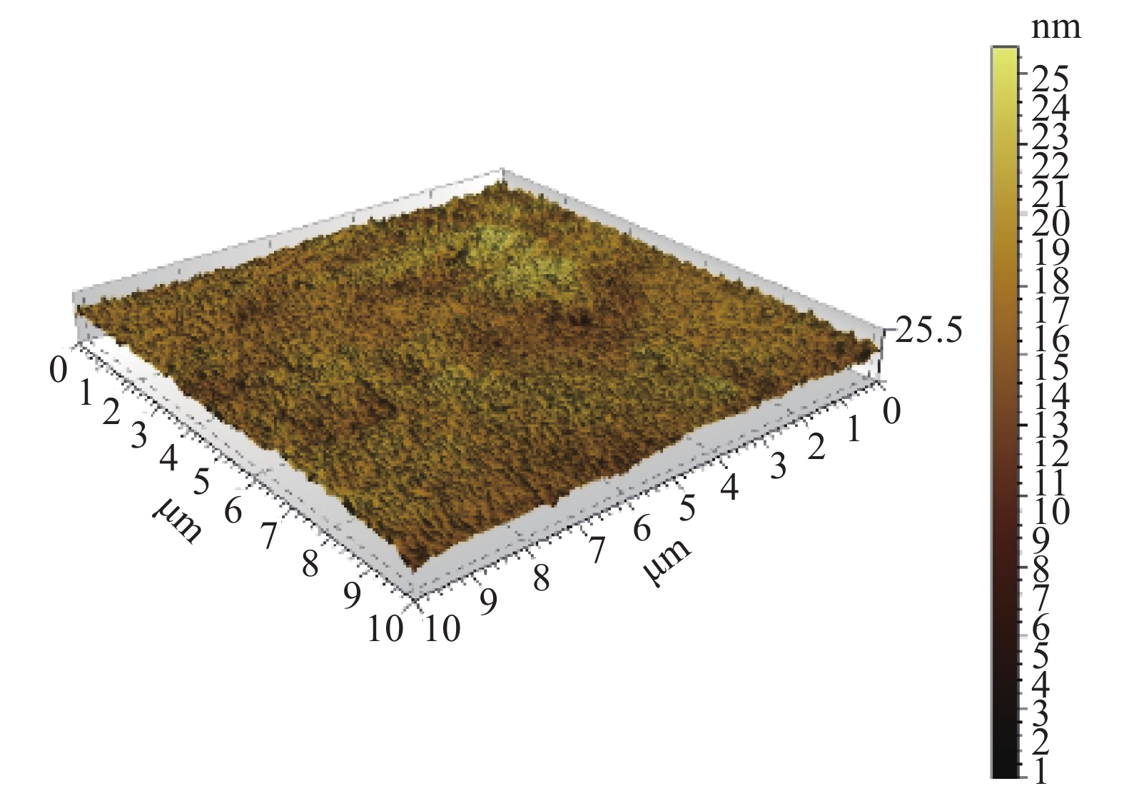
The cleaning of copper interconnect chemical mechanical polishing (CMP) is a key process in integrated circuits (ICs) fabrication. Colloidal silica, which is used as the abrasive material in copper CMP slurry, is considered as the main particle contamination. Abrasive particle residuals can cause device failure which need to be removed efficiently. In this paper, a type of CMP cleaner was used for particle removal using a cleaning solution consisting of FA/O II chelating agent and FA/O I surfactant. By varying the parameters of brush rotation speed, brush gap, and de-ionized water (DIW) flow rate, a series of experiments were performed to determine the best cleaning results. Atomic force microscope (AFM) measurement was used to characterise the surface morphology of the copper surface and the removal of abrasive particles. A scanning electron microscope (SEM) with EDX was used to observe and analyze the particles shape and elements. The optima parameters of CMP cleaner were obtained. Under those conditions, the abrasive silica particles were removed effectively.
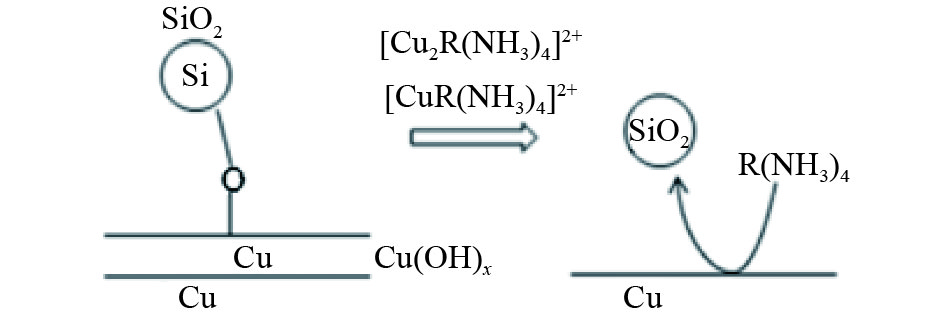
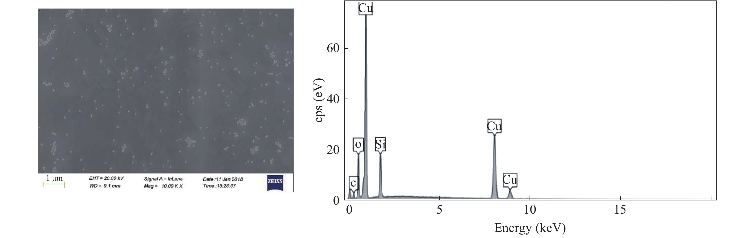
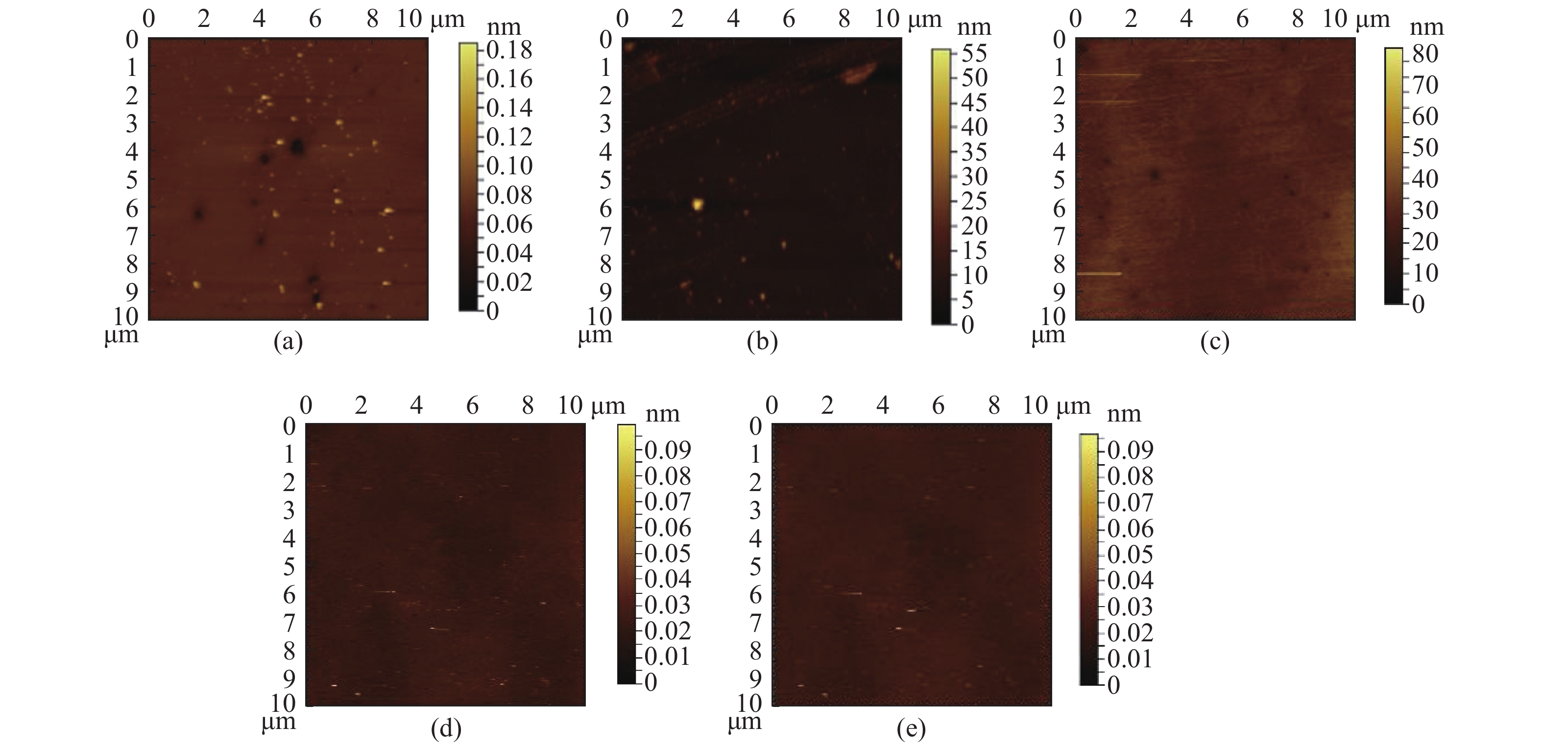


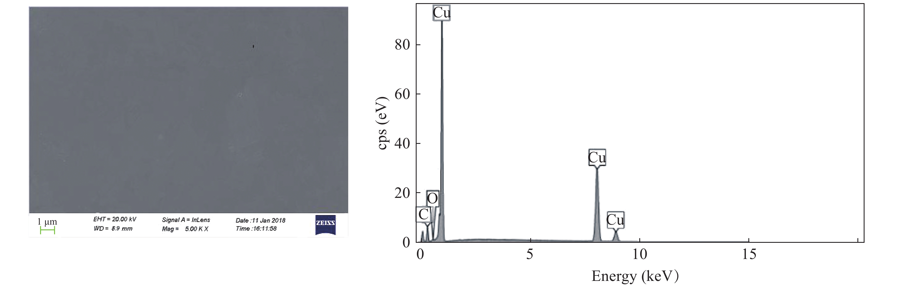
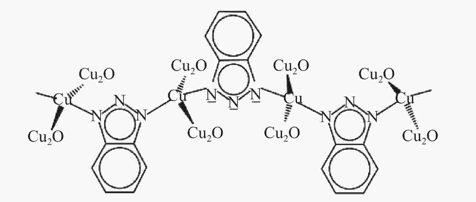
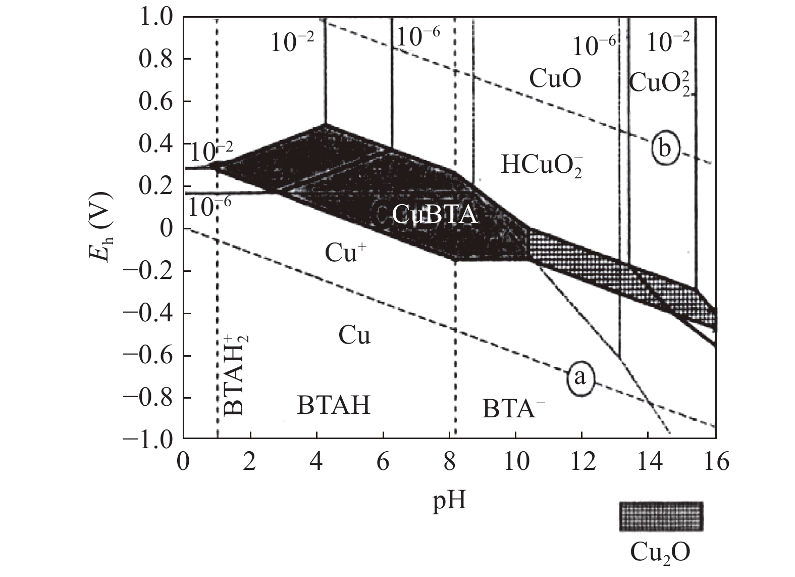
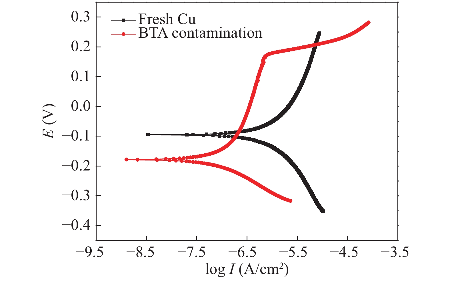
Benzotriazole (BTA), an anticorrosion agent of slurry, is the main organic pollutant remaining after CMP of multilayer copper wiring, and also the main removal object of post CMP cleaning. The adsorption of BTA onto the copper could form a dense Cu-BTA film, which makes the copper surface strongly passivated. According to this characteristic, quantitative analysis of BTA residue after cleaning is carried out by contact angle measurement and electrochemical measurement in this paper. A scanning electron microscope (SEM) with EDX was used to observe and analyze the BTA shape and elements. The efficiencies of organic alkali and inorganic alkali on the removal of BTA were studied. The corresponding reaction mechanism was also analyzed. The results show that the adsorption structure of Cu(I)-BTA cannot be destroyed in an alkaline environment with a pH less than 10; the effect of BTA removal by inorganic alkali is worse than that of the organic amine alkali with the coordination structure under the same pH environment; the FA/O II chelating agent with the fraction of 200 ppm can effectively remove BTA residue on the surface of copper wafer.