


Fig. 1.
(Color online) Device structure of (a) S-TMOS and (b) C-TMOS.
ARTICLES
Xiaorong Luo1, , Ke Zhang1, Xu Song1, Jian Fang1, Fei Yang2 and Bo Zhang1
Corresponding author: Xiaorong Luo, Email: xrluo@uestc.edu.cn
Abstract: A novel 4H-SiC trench MOSFET is presented and investigated by simulation in this paper. The device features an integrated Schottky barrier diode and an L-shaped P+ shielding region beneath the gate trench and aside one wall of the gate trench (S-TMOS). The integrated Schottky barrier diode works as a free-wheeling diode in reverse recovery and reverse conduction, which significantly reduces reverse recovery charge (Qrr) and reverse turn-on voltage (VF). The L-shaped P+ region effectively shields the coupling of gate and drain, resulting in a lower gate–drain capacitance (Cgd) and date–drain charge (Qgd). Compared with that of conventional SiC trench MOSFET (C-TMOS), the VF and Qrr of S-TMOS has reduced by 44% and 75%, respectively, with almost the same forward output current and reverse breakdown voltage. Moreover, the S-TMOS reduces Qgd and Cgd by 32% and 22%, respectively, in comparison with C-TMOS.
Key words: SiC, MOSFET, Schottky barrier diode, reverse recovery, gate-drain charge
| [1] |
Gendron-Hansen A, Sdrulla D, Kashyap A, et al. 4H-SiC junction barrier Schottky diodes and power MOSFETs with high repetitive UIS ruggedness. IEEE Energy Conversion Congress and Exposition (ECCE), 2018, 850
|
| [2] |
Jiang H, Wei J, Dai X, et al. SiC MOSFET with built-in SBD for reduction of reverse recovery charge and switching loss in 10-kV applications. 29th International Symposium on Power Semiconductor Devices and IC's (ISPSD), 2017, 49
|
| [3] |
Jiang H, Wei J, Dai X, et al. Silicon carbide split-gate MOSFET with merged Schottky barrier diode and reduced switching loss. 28th International Symposium on Power Semiconductor Devices and IC's (ISPSD), 2016, 59
|
| [4] |
Li X, Tong X, Huang A Q, et al. SiC trench MOSFET with integrated self-assembled three-level protection Schottky barrier diode. IEEE Trans Electron Devices, 2017, 65(1), 347 doi: 10.1109/TED.2017.2767904
|
| [5] |
Kobayashi Y, Ishimori H, Kinoshita A, et al. Evaluation of Schottky barrier height on 4H-SiC m-face {1
|
| [6] |
He Q, Luo X, Liao T, et al. 4H-SiC superjunction trench MOSFET with reduced saturation current. Superlattices Microstruct, 2019, 125, 58 doi: 10.1016/j.spmi.2018.10.016
|
| [7] |
Luo X R, Liao T, Wei J, et al. A novel 4H-SiC trench MOSFET with double shielding structures and ultralow gate-drain charge. J Semicond, 2019, 40(5), 052803 doi: 10.1088/1674-4926/40/5/052803
|
| [8] |
Zhang M, Wei J, Jiang H, et al. A new SiC trench MOSFET structure with protruded p-base for low oxide field and enhanced switching performance. IEEE Trans Device Mater Reliab, 2017, 17(2), 432 doi: 10.1109/TDMR.2017.2694220
|
| [9] |
Han K, Baliga B J, Sung W. A novel 1.2 kV 4H-SiC buffered-gate (BG) MOSFET: Analysis and experimental results. IEEE Electron Device Lett, 2017, 39(2), 248 doi: 10.1109/LED.2017.2785771
|
| [10] |
Agarwal A, Han K, Baliga B J. Analysis of 1.2 kV 4H-SiC trench-gate MOSFETs with thick trench bottom oxide. 2018 IEEE 6th Workshop on Wide Bandgap Power Devices and Applications (WiPDA), 2018, 125
|
| [11] |
Jiang H, Wei J, Dai X, et al. SiC trench MOSFET with shielded fin-shaped gate to reduce oxide field and switching loss. IEEE Electron Device Lett, 2016, 37(10), 1324 doi: 10.1109/LED.2016.2599921
|
| [12] |
Peters D, Siemieniec R, Aichinger T, et al. Performance and ruggedness of 1200 V SiC-trench- MOSFET. 29th International Symposium on Power Semiconductor Devices and IC's (ISPSD), 2017
|
| [13] |
Lide D R. CRC handbook of chemistry and physics. Internet version 2005. Boca Raton: CRC Press, 2005
|
| [14] |
Heer D, Domes D, Peters D. Switching performance of a 1200 V SiC-trench-MOSFET in a low-power module. International Exhibition and Conference for Power Electronics, Intelligent Motion, Renewable Energy and Energy Management, 2016, 1
|
| [15] |
Lutz J, Schlangenotto H, Scheuermann U, et al. Semiconductor power devices: Physics, characteristics, reliability. Electron Power, 2011, 24(8), 599 doi: 10.1109/MPEL.2018.2886116
|
| [16] |
Zhou X, Yue R, Zhang J, et al. 4H-SiC trench MOSFET with floating/grounded junction barrier-controlled gate structure. IEEE Trans Electron Devices, 2017, 64(11), 4568 doi: 10.1109/TED.2017.2755721
|
| [17] |
Sung W, Baliga B J. Monolithically integrated 4H-SiC MOSFET and JBS diode (JBSFET) using a single ohmic/Schottky process scheme. IEEE Electron Device Lett, 2016, 37(12), 1605 doi: 10.1109/LED.2016.2618720
|
| [18] |
Sung W, Baliga B J. On developing one-chip integration of 1.2 kV SiC MOSFET and JBS diode (JBSFET). IEEE Trans Ind Electrons, 2017, 64(10), 8206 doi: 10.1109/TIE.2017.2696515
|

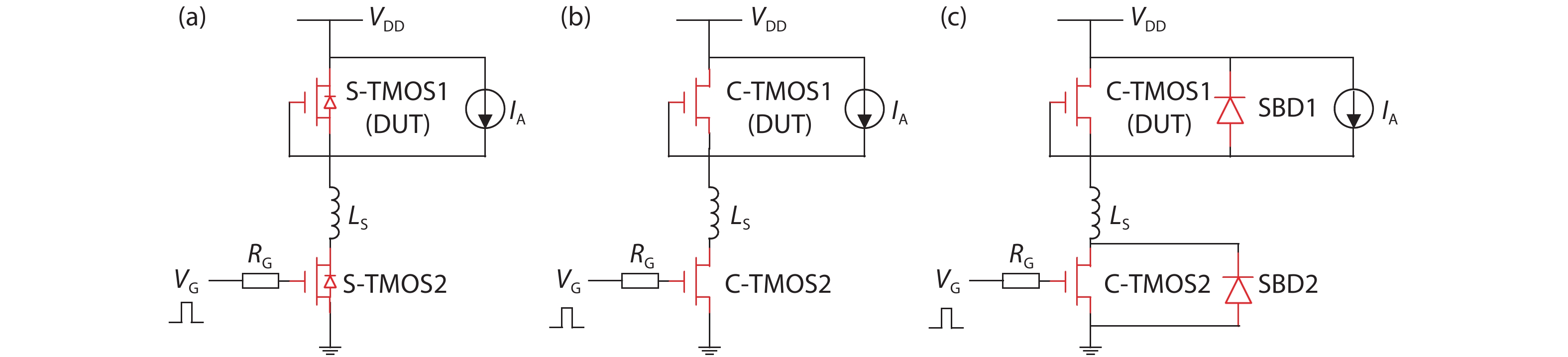

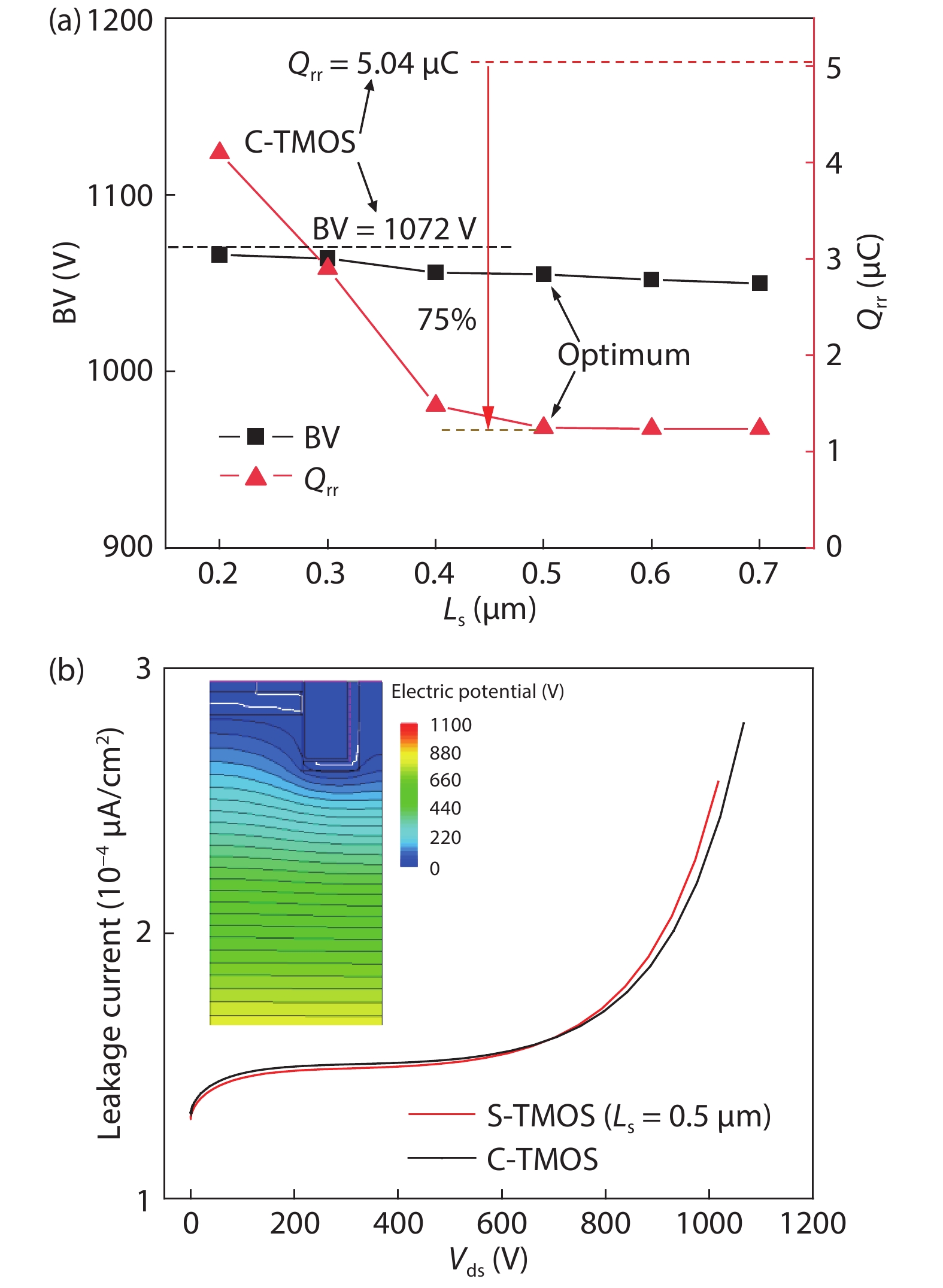
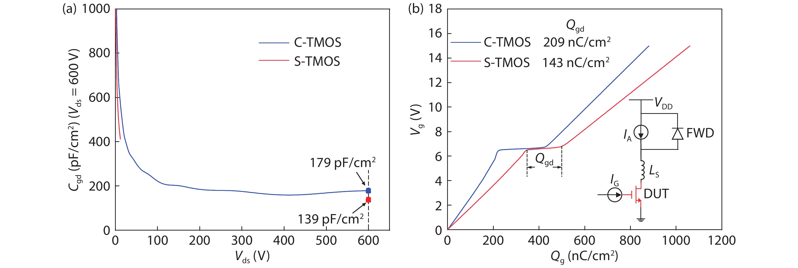
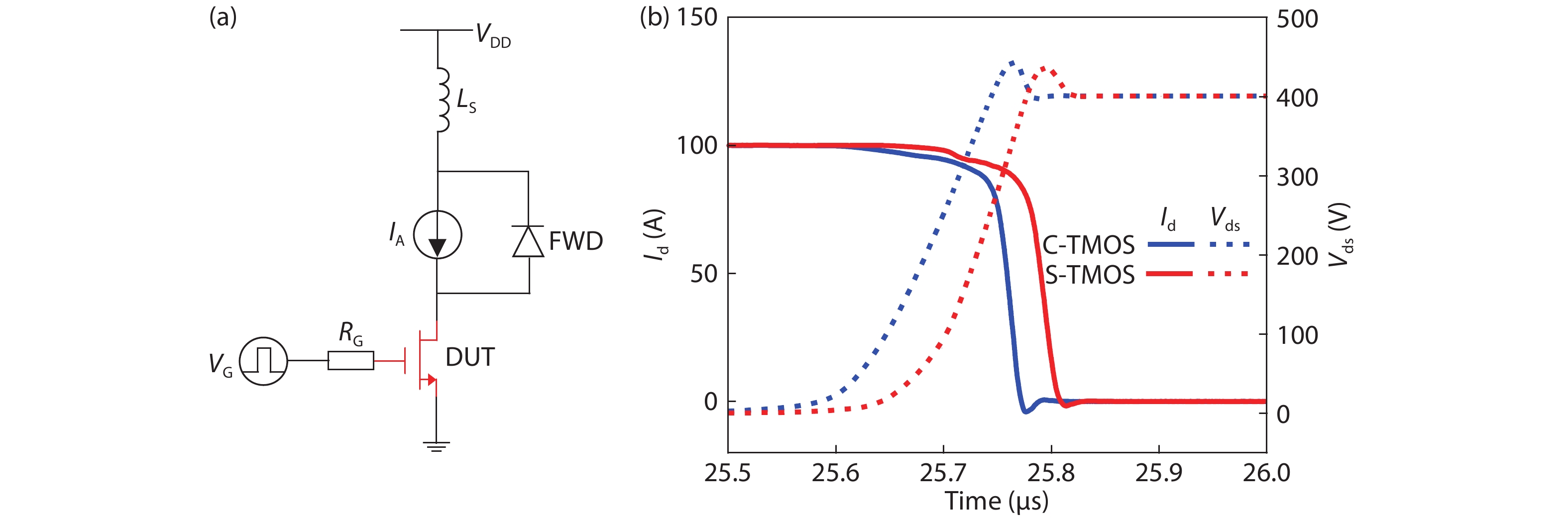

Table 1. Performance comparison of C-TMOS and S-TMOS.
| Parameter | S-TMOS | C-TMOS |
| Ron,sp (mΩ·cm2) | 4.44 | 3.71 |
| BV (V) | 1055 | 1072 |
| VF (V) | 1.5 | 2.7 |
| Qrr (µC) | 1.25 | 5.04 |
| Cgd (pF/cm2) (@ Vds = 600 V) | 139 | 179 |
| Qgd (nC/cm2) | 143 | 209 |
| Eoff (mJ/cm2) | 2.49 | 3.08 |
| Eon + Eoff (mJ/cm2) | 4.50 | 5.16 |
 DownLoad: CSV
| [1] |
Gendron-Hansen A, Sdrulla D, Kashyap A, et al. 4H-SiC junction barrier Schottky diodes and power MOSFETs with high repetitive UIS ruggedness. IEEE Energy Conversion Congress and Exposition (ECCE), 2018, 850
|
| [2] |
Jiang H, Wei J, Dai X, et al. SiC MOSFET with built-in SBD for reduction of reverse recovery charge and switching loss in 10-kV applications. 29th International Symposium on Power Semiconductor Devices and IC's (ISPSD), 2017, 49
|
| [3] |
Jiang H, Wei J, Dai X, et al. Silicon carbide split-gate MOSFET with merged Schottky barrier diode and reduced switching loss. 28th International Symposium on Power Semiconductor Devices and IC's (ISPSD), 2016, 59
|
| [4] |
Li X, Tong X, Huang A Q, et al. SiC trench MOSFET with integrated self-assembled three-level protection Schottky barrier diode. IEEE Trans Electron Devices, 2017, 65(1), 347 doi: 10.1109/TED.2017.2767904
|
| [5] |
Kobayashi Y, Ishimori H, Kinoshita A, et al. Evaluation of Schottky barrier height on 4H-SiC m-face {1
|
| [6] |
He Q, Luo X, Liao T, et al. 4H-SiC superjunction trench MOSFET with reduced saturation current. Superlattices Microstruct, 2019, 125, 58 doi: 10.1016/j.spmi.2018.10.016
|
| [7] |
Luo X R, Liao T, Wei J, et al. A novel 4H-SiC trench MOSFET with double shielding structures and ultralow gate-drain charge. J Semicond, 2019, 40(5), 052803 doi: 10.1088/1674-4926/40/5/052803
|
| [8] |
Zhang M, Wei J, Jiang H, et al. A new SiC trench MOSFET structure with protruded p-base for low oxide field and enhanced switching performance. IEEE Trans Device Mater Reliab, 2017, 17(2), 432 doi: 10.1109/TDMR.2017.2694220
|
| [9] |
Han K, Baliga B J, Sung W. A novel 1.2 kV 4H-SiC buffered-gate (BG) MOSFET: Analysis and experimental results. IEEE Electron Device Lett, 2017, 39(2), 248 doi: 10.1109/LED.2017.2785771
|
| [10] |
Agarwal A, Han K, Baliga B J. Analysis of 1.2 kV 4H-SiC trench-gate MOSFETs with thick trench bottom oxide. 2018 IEEE 6th Workshop on Wide Bandgap Power Devices and Applications (WiPDA), 2018, 125
|
| [11] |
Jiang H, Wei J, Dai X, et al. SiC trench MOSFET with shielded fin-shaped gate to reduce oxide field and switching loss. IEEE Electron Device Lett, 2016, 37(10), 1324 doi: 10.1109/LED.2016.2599921
|
| [12] |
Peters D, Siemieniec R, Aichinger T, et al. Performance and ruggedness of 1200 V SiC-trench- MOSFET. 29th International Symposium on Power Semiconductor Devices and IC's (ISPSD), 2017
|
| [13] |
Lide D R. CRC handbook of chemistry and physics. Internet version 2005. Boca Raton: CRC Press, 2005
|
| [14] |
Heer D, Domes D, Peters D. Switching performance of a 1200 V SiC-trench-MOSFET in a low-power module. International Exhibition and Conference for Power Electronics, Intelligent Motion, Renewable Energy and Energy Management, 2016, 1
|
| [15] |
Lutz J, Schlangenotto H, Scheuermann U, et al. Semiconductor power devices: Physics, characteristics, reliability. Electron Power, 2011, 24(8), 599 doi: 10.1109/MPEL.2018.2886116
|
| [16] |
Zhou X, Yue R, Zhang J, et al. 4H-SiC trench MOSFET with floating/grounded junction barrier-controlled gate structure. IEEE Trans Electron Devices, 2017, 64(11), 4568 doi: 10.1109/TED.2017.2755721
|
| [17] |
Sung W, Baliga B J. Monolithically integrated 4H-SiC MOSFET and JBS diode (JBSFET) using a single ohmic/Schottky process scheme. IEEE Electron Device Lett, 2016, 37(12), 1605 doi: 10.1109/LED.2016.2618720
|
| [18] |
Sung W, Baliga B J. On developing one-chip integration of 1.2 kV SiC MOSFET and JBS diode (JBSFET). IEEE Trans Ind Electrons, 2017, 64(10), 8206 doi: 10.1109/TIE.2017.2696515
|


Article views: 6409 Times PDF downloads: 302 Times Cited by: 0 Times
Received: 13 December 2019 Revised: 08 January 2020 Online: Accepted Manuscript: 29 February 2020Uncorrected proof: 04 March 2020Published: 01 October 2020
| Citation: |
Xiaorong Luo, Ke Zhang, Xu Song, Jian Fang, Fei Yang, Bo Zhang. 4H-SiC trench MOSFET with an integrated Schottky barrier diode and L-shaped P+ shielding region[J]. Journal of Semiconductors, 2020, 41(10): 102801. doi: 10.1088/1674-4926/41/10/102801
****
X R Luo, K Zhang, X Song, J Fang, F Yang, B Zhang, 4H-SiC trench MOSFET with an integrated Schottky barrier diode and L-shaped P+ shielding region[J]. J. Semicond., 2020, 41(10): 102801. doi: 10.1088/1674-4926/41/10/102801.

|
| [1] |
Gendron-Hansen A, Sdrulla D, Kashyap A, et al. 4H-SiC junction barrier Schottky diodes and power MOSFETs with high repetitive UIS ruggedness. IEEE Energy Conversion Congress and Exposition (ECCE), 2018, 850
|
| [2] |
Jiang H, Wei J, Dai X, et al. SiC MOSFET with built-in SBD for reduction of reverse recovery charge and switching loss in 10-kV applications. 29th International Symposium on Power Semiconductor Devices and IC's (ISPSD), 2017, 49
|
| [3] |
Jiang H, Wei J, Dai X, et al. Silicon carbide split-gate MOSFET with merged Schottky barrier diode and reduced switching loss. 28th International Symposium on Power Semiconductor Devices and IC's (ISPSD), 2016, 59
|
| [4] |
Li X, Tong X, Huang A Q, et al. SiC trench MOSFET with integrated self-assembled three-level protection Schottky barrier diode. IEEE Trans Electron Devices, 2017, 65(1), 347 doi: 10.1109/TED.2017.2767904
|
| [5] |
Kobayashi Y, Ishimori H, Kinoshita A, et al. Evaluation of Schottky barrier height on 4H-SiC m-face {1
|
| [6] |
He Q, Luo X, Liao T, et al. 4H-SiC superjunction trench MOSFET with reduced saturation current. Superlattices Microstruct, 2019, 125, 58 doi: 10.1016/j.spmi.2018.10.016
|
| [7] |
Luo X R, Liao T, Wei J, et al. A novel 4H-SiC trench MOSFET with double shielding structures and ultralow gate-drain charge. J Semicond, 2019, 40(5), 052803 doi: 10.1088/1674-4926/40/5/052803
|
| [8] |
Zhang M, Wei J, Jiang H, et al. A new SiC trench MOSFET structure with protruded p-base for low oxide field and enhanced switching performance. IEEE Trans Device Mater Reliab, 2017, 17(2), 432 doi: 10.1109/TDMR.2017.2694220
|
| [9] |
Han K, Baliga B J, Sung W. A novel 1.2 kV 4H-SiC buffered-gate (BG) MOSFET: Analysis and experimental results. IEEE Electron Device Lett, 2017, 39(2), 248 doi: 10.1109/LED.2017.2785771
|
| [10] |
Agarwal A, Han K, Baliga B J. Analysis of 1.2 kV 4H-SiC trench-gate MOSFETs with thick trench bottom oxide. 2018 IEEE 6th Workshop on Wide Bandgap Power Devices and Applications (WiPDA), 2018, 125
|
| [11] |
Jiang H, Wei J, Dai X, et al. SiC trench MOSFET with shielded fin-shaped gate to reduce oxide field and switching loss. IEEE Electron Device Lett, 2016, 37(10), 1324 doi: 10.1109/LED.2016.2599921
|
| [12] |
Peters D, Siemieniec R, Aichinger T, et al. Performance and ruggedness of 1200 V SiC-trench- MOSFET. 29th International Symposium on Power Semiconductor Devices and IC's (ISPSD), 2017
|
| [13] |
Lide D R. CRC handbook of chemistry and physics. Internet version 2005. Boca Raton: CRC Press, 2005
|
| [14] |
Heer D, Domes D, Peters D. Switching performance of a 1200 V SiC-trench-MOSFET in a low-power module. International Exhibition and Conference for Power Electronics, Intelligent Motion, Renewable Energy and Energy Management, 2016, 1
|
| [15] |
Lutz J, Schlangenotto H, Scheuermann U, et al. Semiconductor power devices: Physics, characteristics, reliability. Electron Power, 2011, 24(8), 599 doi: 10.1109/MPEL.2018.2886116
|
| [16] |
Zhou X, Yue R, Zhang J, et al. 4H-SiC trench MOSFET with floating/grounded junction barrier-controlled gate structure. IEEE Trans Electron Devices, 2017, 64(11), 4568 doi: 10.1109/TED.2017.2755721
|
| [17] |
Sung W, Baliga B J. Monolithically integrated 4H-SiC MOSFET and JBS diode (JBSFET) using a single ohmic/Schottky process scheme. IEEE Electron Device Lett, 2016, 37(12), 1605 doi: 10.1109/LED.2016.2618720
|
| [18] |
Sung W, Baliga B J. On developing one-chip integration of 1.2 kV SiC MOSFET and JBS diode (JBSFET). IEEE Trans Ind Electrons, 2017, 64(10), 8206 doi: 10.1109/TIE.2017.2696515
|

 WeChat ID
Journal of Semiconductors © 2017 All Rights Reserved 京ICP备05085259号-2


