ARTICLES

Theoretical study of a group IV p–i–n photodetector with a flat and broad response for visible and infrared detection

Jinyong Wu1, Donglin Huang1, Yujie Ye1, Jianyuan Wang1, Wei Huang1, Cheng Li1, Songyan Chen1, and Shaoying Ke2,

+ Author Affiliations

 Corresponding author: Songyan Chen, Email: sychen@xmu.edu.cn; Shaoying Ke, keshaoying2005@163.com

PDF

Turn off MathJax

Abstract: We report a theoretical study of a broadband Si/graded-SiGe/Ge/Ge0.9Sn0.1 p–i–n photodetector with a flat response based on modulating thickness of the layers in the active region. The responsivity of the photodetector is about 0.57 A/W in the range of 700 to 1800 nm. This structure is suitable for silicon-based epitaxial growth. Annealing is technically applied to form the graded-SiGe. The photodetector reaches a cut-off wavelength at ~2300 nm and a low dark-current density under 3 V reverse bias about 0.17 mA/cm2 is achieved theoretical at room temperature. This work is of great significance for silicon-based detection and communication, from visible to infrared.

Key words: flat responsebroad responsedark current densitygraded-SiGeGe0.9Sn0.1


[1]
Eda G, Fanchini G, Chhowalla M. Large-area ultrathin films of reduced graphene oxide as a transparent and flexible electronic material. Nat Nanotechnol, 2008, 3, 270 doi: 10.1038/nnano.2008.83
[2]
Park S, Wang G, Cho B, et al. Flexible molecular-scale electronic devices. Nat Nanotechnol, 2012, 7, 438 doi: 10.1038/nnano.2012.81
[3]
de Arquer F P G, Armin A, Meredith P, et al. Solution-processed semiconductors for next-generation photodetectors. Nat Rev Mater, 2017, 2, 16100 doi: 10.1038/natrevmats.2016.100
[4]
Gong X, Tong M, Xia Y, et al. High-detectivity polymer photodetectors with spectral response from 300 nm to 1450 nm. Science, 2009, 325, 1665 doi: 10.1126/science.1176706
[5]
Qiao H, Yuan J, Xu Z Q, et al. Broadband photodetectors based on graphene–Bi2Te3 heterostructure. ACS Nano, 2015, 9, 1886 doi: 10.1021/nn506920z
[6]
Yuan H, Liu X, Afshinmanesh F, et al. Polarization-sensitive broadband photodetector using a black phosphorus vertical p–n junction. Nat Nanotechnol, 2015, 10, 707 doi: 10.1038/nnano.2015.112
[7]
Hu W, Cong H, Huang W, et al. Germanium/perovskite heterostructure for high-performance and broadband photodetector from visible to infrared telecommunication band. Light: Sci Appl, 2019, 8, 106 doi: 10.1038/s41377-019-0218-y
[8]
Eckhardt C, Hummer K, Kresse G. Indirect-to-direct gap transition in strained and unstrained SnxGe1–x alloys. Phys Rev B, 2014, 89, 165201 doi: 10.1103/PhysRevB.89.165201
[9]
Du W, Ghetmiri S A, Conley B R, et al. Competition of optical transitions between direct and indirect bandgaps in Ge1−xSnx. Appl Phys Lett, 2014, 105, 051104 doi: 10.1063/1.4892302
[10]
Gassenq A, Gencarelli F, van Campenhout J, et al. GeSn/Ge heterostructure short-wave infrared photodetectors on silicon. Opt Express, 2012, 20, 27297 doi: 10.1364/OE.20.027297
[11]
Cong H, Xue C L, Zheng J, et al. Silicon based GeSn p–i–n photodetector for SWIR detection. IEEE Photonics J, 2016, 8, 1 doi: 10.1109/JPHOT.2016.2607687
[12]
Su S J, Cheng B W, Xue C L, et al. GeSn p–i–n photodetector for all telecommunication bands detection. Optics Express, 2011, 19, 6400 doi: 10.1364/OE.19.006400
[13]
Mathews J, Roucka R, Xie J, et al. Extended performance GeSn/Si(100) p–i–n photodetectors for full spectral range telecommunication applications. Appl Phys Lett, 2009, 95, 133506 doi: 10.1063/1.3238327
[14]
Kouvetakis J, Menendez J, Chizmeshya A V G. Tin-based group IV semiconductors: New platforms for opto- and microelectronics on silicon. Annu Rev Mater Res, 2006, 36, 497 doi: 10.1146/annurev.matsci.36.090804.095159
[15]
Ke S Y, Ye Y J, Lin S M, et al. Low-temperature oxide-free silicon and germanium wafer bonding based on a sputtered amorphous Ge. Appl Phys Lett, 2018, 112, 041601 doi: 10.1063/1.4996800
[16]
Ke S Y, Ye Y J, Wu J Y, et al. Interface characteristics and electrical transport of Ge/Si heterojunction fabricated by low-temperature wafer bonding. J Phys D, 2018, 51, 265306 doi: 10.1088/1361-6463/aac7b0
[17]
Ke S Y, Lin S M, Ye Y J, et al. Bubble evolution mechanism and stress-induced crystallization in low-temperature silicon wafer bonding based on a thin intermediate amorphous Ge layer. J Phys D, 2017, 50, 405305 doi: 10.1088/1361-6463/aa81ee
[18]
Lin Y, Lee K H, Bao S, et al. High-efficiency normal-incidence vertical p–i–n photodetectors on a germanium-on-insulator platform: Publisher's note. Photonics Res, 2018, 6, 46 doi: 10.1364/PRJ.6.000046
[19]
Ghetmiri S A, Du W, Conley B R, et al. Shortwave-infrared photoluminescence from Ge1– xSnx thin films on silicon. J Vac Sci Technol B, 2014, 32, 060601 doi: 10.1116/1.4897917
[20]
Tran H, Du W, Ghetmiri S A, et al. Systematic study of Ge1− xSnx absorption coefficient and refractive index for the device applications of Si-based optoelectronics. J Appl Phys, 2016, 119, 103106 doi: 10.1063/1.4943652
[21]
Masini C, Calace L, Assanto G, et al. High-performance p–i–n Ge on Si photodetectors for the near infrared: From model to demonstration. IEEE Trans Electron Devices, 2001, 48, 1092 doi: 10.1109/16.925232
[22]
Rzaev M, Schäffler F, Vdovin V, et al. Misfit dislocation nucleation and multiplication in fully strained SiGe/Si heterostructures under thermal annealing. Mater Sci Semicond Process, 2005, 8, 137 doi: 10.1016/j.mssp.2004.09.027
[23]
Humlíček J, Garriga M, Alonso M I, et al. Optical spectra of SixGe1–x alloys. J Appl Phys, 1989, 65, 2827 doi: 10.1063/1.342720
[24]
Braunstein R, Moore A R, Herman F. Intrinsic optical absorption in germanium-silicon alloys. Phys Rev, 1958, 109, 695 doi: 10.1103/PhysRev.109.695
[25]
Choi D, Ge Y S, Harris J S, et al. Low surface roughness and threading dislocation density Ge growth on Si (001). J Cryst Growth, 2008, 310, 4273 doi: 10.1016/j.jcrysgro.2008.07.029
[26]
Xia G, Hoyt J L, Canonico M. Si –Ge interdiffusion in strained Si/strained SiGe heterostructures and implications for enhanced mobility metal–oxide–semiconductor field-effect transistors. J Appl Phys, 2007, 101, 044901 doi: 10.1063/1.2430904
[27]
Gavelle M, Bazizi E M, Scheid E, et al. Study of silicon-germanium interdiffusion from pure germanium deposited layers. Mater Sci Eng B, 2008, 154/155, 110 doi: 10.1016/j.mseb.2008.09.015
[28]
Luan H, Lim D R, Lee K K, et al. High-quality Ge epilayers on Si with low threading-dislocation densities. Appl Phys Lett, 1999, 75, 2909 doi: 10.1063/1.125187
[29]
del Alamo J, Swirhun S, Swanson R M. Simultaneous measurement of hole lifetime, hole mobility and bandgap narrowing in heavily doped n-type silicon. Int Electron Devices Meet, 1985, 290
[30]
Kulin S S, Kurtz A D. Effect of dislocations on minority carrier lifetime in germanium. Acta Metall, 1954, 2, 354 doi: 10.1016/0001-6160(54)90186-8
[31]
Zhao Y, Wang N, Yu K, et al. High performance silicon-based GeSn p–i–n photodetectors for short-wave infrared application. Chin Phys B, 2019, 28, 128501 doi: 10.1088/1674-1056/ab4e84
[32]
Kasai I, Hettich H L, Lawrence S L, et al. Wideband anti-reflection coating for indium antimonide photodetector device. European Patent, EP0585055, 1997
[33]
Chang C, Sharma Y D, Kim Y, et al. A surface plasmon enhanced infrared photodetector based on InAs quantum dots. Nano Lett, 2010, 10, 1704 doi: 10.1021/nl100081j
[34]
Yang J K, Seo M K, Hwang I K, et al. Polarization-selective resonant photonic crystal photodetector. Appl Phys Lett, 2008, 93, 211103 doi: 10.1063/1.3036954
[35]
Zhu T F, Liu Z C, Liu Z C, et al. Fabrication of monolithic diamond photodetector with microlenses. Opt Express, 2017, 25, 31586 doi: 10.1364/OE.25.031586
[36]
Zhong H, Guo A R, Guo G H, et al. The enhanced light absorptance and device application of nanostructured black silicon fabricated by metal-assisted chemical etching. Nanoscale Res Lett, 2016, 11, 1 doi: 10.1186/s11671-015-1209-4
Fig. 1.  (Color online) (a) Schematic cross-section of the Si/graded-SiGe/Ge/Ge0.9Sn0.1 p–i–n photodetector. The mesa size is 32 µm in diameter. (b) Schematic of epitaxial growth and layer transfer technique for this p–i–n structure fabrication.

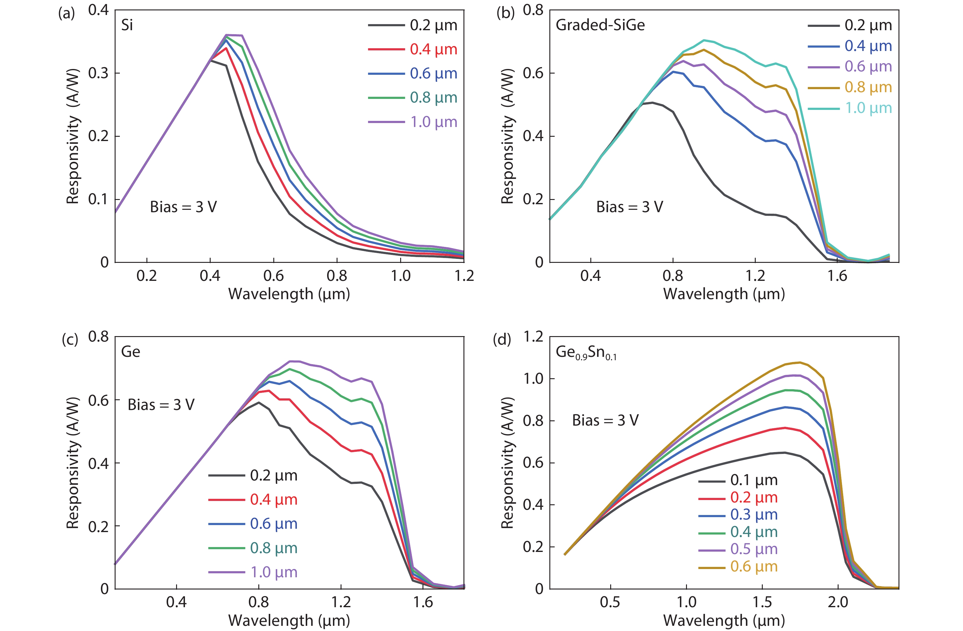
Fig. 2.  (Color online) Simulation of spectral responsivity of the p–i–n photodetector with single material as active region for (a) Si, (b) graded-SiGe, (c) Ge, and (d) Ge0.9Sn0.1.

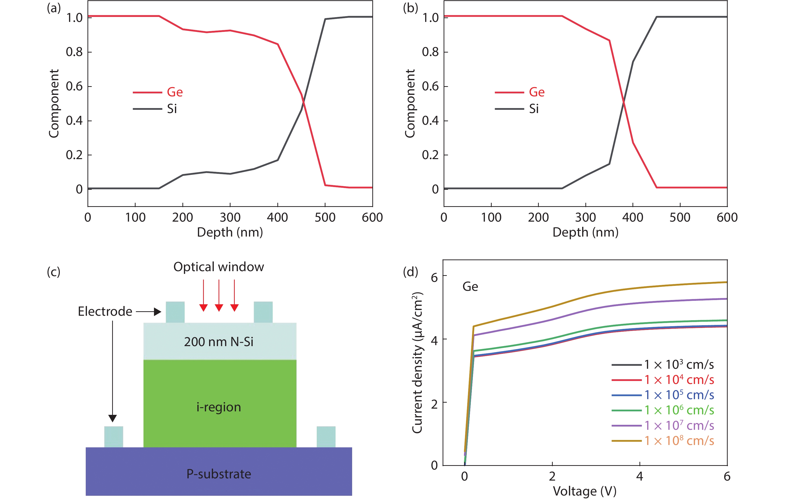
Fig. 3.  (Color online) (a) AES of the sample annealed at 800 °C for 30 min and 900 °C for 0 s. (b) AES of the sample annealed at 800 °C for 30 min and 900 °C for 10 min. (c) Schematic cross-section of the single material p–i–n photodetector. The mesa size is 32 µm in diameter. (d) Influence of SRV on dark current density of Ge p–i–n photodetector.

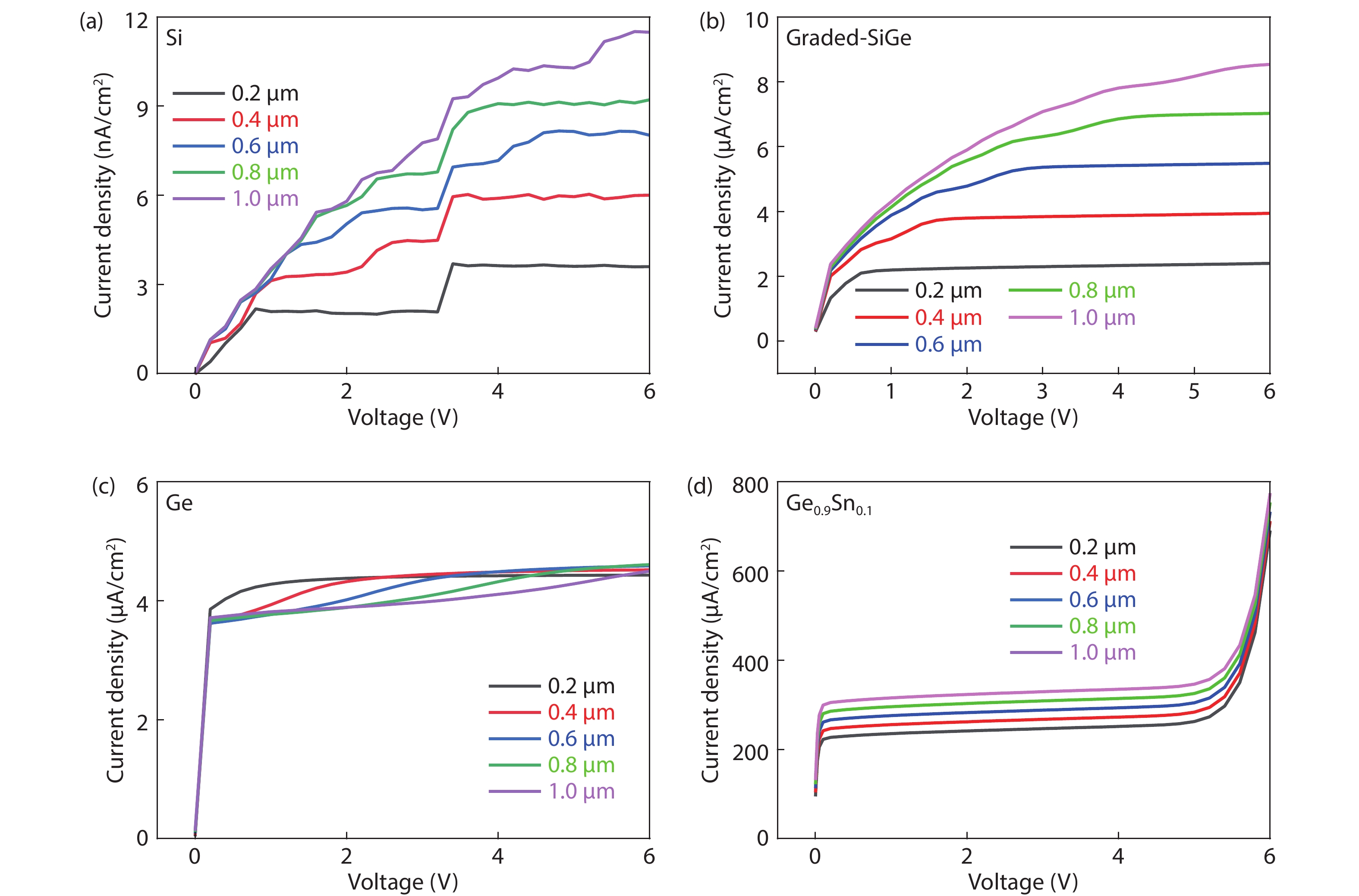
Fig. 4.  (Color online) Simulation of Jdark of the p–i–n photodetector with single material for (a) Si, (b) graded-SiGe, (c) Ge, and (d) Ge0.9Sn0.1.

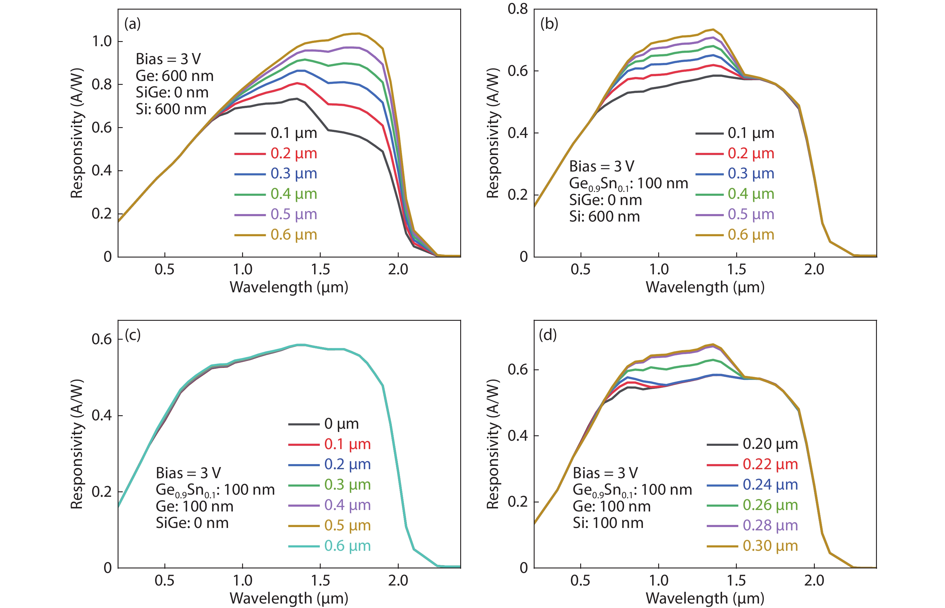
Fig. 5.  (Color online) The variation of responsivity under different active region is simulated for (a) Ge0.9Sn0.1, (b) Ge, (c) Si, and (d) graded-SiGe.

Fig. 6.  (a) Magnitude of the Jdark at different thickness of Ge0.9Sn0.1 layer. (b) The final spectral response of the designed photodetector and the Jdark changes between 0–6 V reverse bias.

Table 1.   Parameters of Si, SiGe, Ge, and Ge0.9Sn0.1.

MaterialEnergy gap (eV)Surface recombination velocity (cm/s)Threading dislocation density (TDD) (cm–2)n, k
Si1.123.5 × 1021 × 104Database
SiGe0.66–1.121 × 1061 × 107[22]Ref. [23, 24]
Ge0.661 × 1061 × 107[25]Database
Ge0.9Sn0.10.4951 × 1061 × 107Ref. [20]
DownLoad: CSV
[1]
Eda G, Fanchini G, Chhowalla M. Large-area ultrathin films of reduced graphene oxide as a transparent and flexible electronic material. Nat Nanotechnol, 2008, 3, 270 doi: 10.1038/nnano.2008.83
[2]
Park S, Wang G, Cho B, et al. Flexible molecular-scale electronic devices. Nat Nanotechnol, 2012, 7, 438 doi: 10.1038/nnano.2012.81
[3]
de Arquer F P G, Armin A, Meredith P, et al. Solution-processed semiconductors for next-generation photodetectors. Nat Rev Mater, 2017, 2, 16100 doi: 10.1038/natrevmats.2016.100
[4]
Gong X, Tong M, Xia Y, et al. High-detectivity polymer photodetectors with spectral response from 300 nm to 1450 nm. Science, 2009, 325, 1665 doi: 10.1126/science.1176706
[5]
Qiao H, Yuan J, Xu Z Q, et al. Broadband photodetectors based on graphene–Bi2Te3 heterostructure. ACS Nano, 2015, 9, 1886 doi: 10.1021/nn506920z
[6]
Yuan H, Liu X, Afshinmanesh F, et al. Polarization-sensitive broadband photodetector using a black phosphorus vertical p–n junction. Nat Nanotechnol, 2015, 10, 707 doi: 10.1038/nnano.2015.112
[7]
Hu W, Cong H, Huang W, et al. Germanium/perovskite heterostructure for high-performance and broadband photodetector from visible to infrared telecommunication band. Light: Sci Appl, 2019, 8, 106 doi: 10.1038/s41377-019-0218-y
[8]
Eckhardt C, Hummer K, Kresse G. Indirect-to-direct gap transition in strained and unstrained SnxGe1–x alloys. Phys Rev B, 2014, 89, 165201 doi: 10.1103/PhysRevB.89.165201
[9]
Du W, Ghetmiri S A, Conley B R, et al. Competition of optical transitions between direct and indirect bandgaps in Ge1−xSnx. Appl Phys Lett, 2014, 105, 051104 doi: 10.1063/1.4892302
[10]
Gassenq A, Gencarelli F, van Campenhout J, et al. GeSn/Ge heterostructure short-wave infrared photodetectors on silicon. Opt Express, 2012, 20, 27297 doi: 10.1364/OE.20.027297
[11]
Cong H, Xue C L, Zheng J, et al. Silicon based GeSn p–i–n photodetector for SWIR detection. IEEE Photonics J, 2016, 8, 1 doi: 10.1109/JPHOT.2016.2607687
[12]
Su S J, Cheng B W, Xue C L, et al. GeSn p–i–n photodetector for all telecommunication bands detection. Optics Express, 2011, 19, 6400 doi: 10.1364/OE.19.006400
[13]
Mathews J, Roucka R, Xie J, et al. Extended performance GeSn/Si(100) p–i–n photodetectors for full spectral range telecommunication applications. Appl Phys Lett, 2009, 95, 133506 doi: 10.1063/1.3238327
[14]
Kouvetakis J, Menendez J, Chizmeshya A V G. Tin-based group IV semiconductors: New platforms for opto- and microelectronics on silicon. Annu Rev Mater Res, 2006, 36, 497 doi: 10.1146/annurev.matsci.36.090804.095159
[15]
Ke S Y, Ye Y J, Lin S M, et al. Low-temperature oxide-free silicon and germanium wafer bonding based on a sputtered amorphous Ge. Appl Phys Lett, 2018, 112, 041601 doi: 10.1063/1.4996800
[16]
Ke S Y, Ye Y J, Wu J Y, et al. Interface characteristics and electrical transport of Ge/Si heterojunction fabricated by low-temperature wafer bonding. J Phys D, 2018, 51, 265306 doi: 10.1088/1361-6463/aac7b0
[17]
Ke S Y, Lin S M, Ye Y J, et al. Bubble evolution mechanism and stress-induced crystallization in low-temperature silicon wafer bonding based on a thin intermediate amorphous Ge layer. J Phys D, 2017, 50, 405305 doi: 10.1088/1361-6463/aa81ee
[18]
Lin Y, Lee K H, Bao S, et al. High-efficiency normal-incidence vertical p–i–n photodetectors on a germanium-on-insulator platform: Publisher's note. Photonics Res, 2018, 6, 46 doi: 10.1364/PRJ.6.000046
[19]
Ghetmiri S A, Du W, Conley B R, et al. Shortwave-infrared photoluminescence from Ge1– xSnx thin films on silicon. J Vac Sci Technol B, 2014, 32, 060601 doi: 10.1116/1.4897917
[20]
Tran H, Du W, Ghetmiri S A, et al. Systematic study of Ge1− xSnx absorption coefficient and refractive index for the device applications of Si-based optoelectronics. J Appl Phys, 2016, 119, 103106 doi: 10.1063/1.4943652
[21]
Masini C, Calace L, Assanto G, et al. High-performance p–i–n Ge on Si photodetectors for the near infrared: From model to demonstration. IEEE Trans Electron Devices, 2001, 48, 1092 doi: 10.1109/16.925232
[22]
Rzaev M, Schäffler F, Vdovin V, et al. Misfit dislocation nucleation and multiplication in fully strained SiGe/Si heterostructures under thermal annealing. Mater Sci Semicond Process, 2005, 8, 137 doi: 10.1016/j.mssp.2004.09.027
[23]
Humlíček J, Garriga M, Alonso M I, et al. Optical spectra of SixGe1–x alloys. J Appl Phys, 1989, 65, 2827 doi: 10.1063/1.342720
[24]
Braunstein R, Moore A R, Herman F. Intrinsic optical absorption in germanium-silicon alloys. Phys Rev, 1958, 109, 695 doi: 10.1103/PhysRev.109.695
[25]
Choi D, Ge Y S, Harris J S, et al. Low surface roughness and threading dislocation density Ge growth on Si (001). J Cryst Growth, 2008, 310, 4273 doi: 10.1016/j.jcrysgro.2008.07.029
[26]
Xia G, Hoyt J L, Canonico M. Si –Ge interdiffusion in strained Si/strained SiGe heterostructures and implications for enhanced mobility metal–oxide–semiconductor field-effect transistors. J Appl Phys, 2007, 101, 044901 doi: 10.1063/1.2430904
[27]
Gavelle M, Bazizi E M, Scheid E, et al. Study of silicon-germanium interdiffusion from pure germanium deposited layers. Mater Sci Eng B, 2008, 154/155, 110 doi: 10.1016/j.mseb.2008.09.015
[28]
Luan H, Lim D R, Lee K K, et al. High-quality Ge epilayers on Si with low threading-dislocation densities. Appl Phys Lett, 1999, 75, 2909 doi: 10.1063/1.125187
[29]
del Alamo J, Swirhun S, Swanson R M. Simultaneous measurement of hole lifetime, hole mobility and bandgap narrowing in heavily doped n-type silicon. Int Electron Devices Meet, 1985, 290
[30]
Kulin S S, Kurtz A D. Effect of dislocations on minority carrier lifetime in germanium. Acta Metall, 1954, 2, 354 doi: 10.1016/0001-6160(54)90186-8
[31]
Zhao Y, Wang N, Yu K, et al. High performance silicon-based GeSn p–i–n photodetectors for short-wave infrared application. Chin Phys B, 2019, 28, 128501 doi: 10.1088/1674-1056/ab4e84
[32]
Kasai I, Hettich H L, Lawrence S L, et al. Wideband anti-reflection coating for indium antimonide photodetector device. European Patent, EP0585055, 1997
[33]
Chang C, Sharma Y D, Kim Y, et al. A surface plasmon enhanced infrared photodetector based on InAs quantum dots. Nano Lett, 2010, 10, 1704 doi: 10.1021/nl100081j
[34]
Yang J K, Seo M K, Hwang I K, et al. Polarization-selective resonant photonic crystal photodetector. Appl Phys Lett, 2008, 93, 211103 doi: 10.1063/1.3036954
[35]
Zhu T F, Liu Z C, Liu Z C, et al. Fabrication of monolithic diamond photodetector with microlenses. Opt Express, 2017, 25, 31586 doi: 10.1364/OE.25.031586
[36]
Zhong H, Guo A R, Guo G H, et al. The enhanced light absorptance and device application of nanostructured black silicon fabricated by metal-assisted chemical etching. Nanoscale Res Lett, 2016, 11, 1 doi: 10.1186/s11671-015-1209-4
  • Search

    Advanced Search >>

    GET CITATION

    shu

    Export: BibTex EndNote

    Article Metrics

    Article views: 3227 Times PDF downloads: 58 Times Cited by: 0 Times

    History

    Received: 12 March 2020 Revised: 28 April 2020 Online: Accepted Manuscript: 13 July 2020Uncorrected proof: 16 July 2020Published: 08 December 2020

    Catalog

      Email This Article

      User name:
      Email:*请输入正确邮箱
      Code:*验证码错误
      Jinyong Wu, Donglin Huang, Yujie Ye, Jianyuan Wang, Wei Huang, Cheng Li, Songyan Chen, Shaoying Ke. Theoretical study of a group IV p–i–n photodetector with a flat and broad response for visible and infrared detection[J]. Journal of Semiconductors, 2020, 41(12): 122402. doi: 10.1088/1674-4926/41/12/122402 J Y Wu, D L Huang, Y J Ye, J Y Wang, W Huang, C Li, S Y Chen, S Y Ke, Theoretical study of a group IV p–i–n photodetector with a flat and broad response for visible and infrared detection[J]. J. Semicond., 2020, 41(12): 122402. doi: 10.1088/1674-4926/41/12/122402.Export: BibTex EndNote
      Citation:
      Jinyong Wu, Donglin Huang, Yujie Ye, Jianyuan Wang, Wei Huang, Cheng Li, Songyan Chen, Shaoying Ke. Theoretical study of a group IV p–i–n photodetector with a flat and broad response for visible and infrared detection[J]. Journal of Semiconductors, 2020, 41(12): 122402. doi: 10.1088/1674-4926/41/12/122402

      J Y Wu, D L Huang, Y J Ye, J Y Wang, W Huang, C Li, S Y Chen, S Y Ke, Theoretical study of a group IV p–i–n photodetector with a flat and broad response for visible and infrared detection[J]. J. Semicond., 2020, 41(12): 122402. doi: 10.1088/1674-4926/41/12/122402.
      Export: BibTex EndNote

      Theoretical study of a group IV p–i–n photodetector with a flat and broad response for visible and infrared detection

      doi: 10.1088/1674-4926/41/12/122402
      More Information

      Catalog

        /

        DownLoad:  Full-Size Img  PowerPoint
        Return
        Return