Fig. 1.
(Color online) Schematic cross section of the (a) proposed DS-MOS, (b) DT-MOS, and (c) CT-MOS.
ARTICLES
Xiaorong Luo1, , Tian Liao1, Jie Wei1, Jian Fang1, Fei Yang2 and Bo Zhang1
Corresponding author: Xiaorong Luo, Email: xrluo@uestc.edu.cn
Abstract: A new ultralow gate–drain charge (QGD) 4H-SiC trench MOSFET is presented and its mechanism is investigated by simulation. The novel MOSFET features double shielding structures (DS-MOS): one is the grounded split gate (SG), the other is the P+ shielding region (PSR). Both the SG and the PSR reduce the coupling effect between the gate and the drain, and transform the most part of the gate–drain capacitance (CGD) into the gate–source capacitance (CGS) and drain–source capacitance (CDS) in series. Thus the CGD is reduced and the proposed DS-MOS obtains ultralow QGD. Compared with the double-trench MOSFET (DT-MOS) and the conventional trench MOSFET (CT-MOS), the proposed DS-MOS decreases the QGD by 85% and 81%, respectively. Moreover, the figure of merit (FOM), defined as the product of specific on-resistance (Ron, sp) and QGD (Ron, spQGD), is reduced by 84% and 81%, respectively.
Key words: SiC trench MOSFET, reverse transfer capacitance, gate-drain charge, figure of merit
| [1] |
Pittini R, Zhang Z, Andersen M A E. Switching performance evaluation of commercial SiC power devices (SiC JFET and SiC MOSFET) in relation to the gate driver complexity. IEEE ECCE Asia Downunder, 2013, 233
|
| [2] |
Zhang X, Yao C, Li C, et al. A wide bandgap device-based isolated quasi-switched-capacitor DC/DC converter. IEEE Trans Power Electron, 2014, 29(5), 2500 doi: 10.1109/TPEL.2013.2287501
|
| [3] |
Abbatelli L, Macauda M, Catalisano G, et al. Cost benefits on high frequency converter system based on SiC MOSFET approach. PCIM Europe; International Exhibition and Conference for Power Electronics, Intelligent Motion, Renewable Energy and Energy Management, 2014, 1
|
| [4] |
T Kimoto, J A Cooper. Fundamentals of silicon carbide technology: growth, characterization, devices, and applications. Singapore: Wiley, 2014
|
| [5] |
Tega N, Hisamoto D, Shima A, et al. Channel properties of SiC trench-etched double-implanted MOS (TED MOS). IEEE Trans Electron Devices, 2016, 63(9), 1 doi: 10.1109/ted.2016.2587799
|
| [6] |
Zhang Q, Gomez M. 1600V 4H-SiC UMOSFETs with dual buffer layers. International Symposium on Power Semiconductor Devices and ICs, 2005, 211
|
| [7] |
Sui Y, Tsuji T, Cooper J A. On-state characteristics of SiC power UMOSFETs on 115-μm drift layers. IEEE Electron Device Lett, 2005, 26(4), 255 doi: 10.1109/LED.2005.845495
|
| [8] |
Tega N, Yoshimoto H,Hisamoto D, et al. Novel trench-etched double-diffused SiC MOS (TED MOS) for overcoming tradeoff between RonA and Qgd. International Symposium on Power Semiconductor Devices and ICs, 2015, 81
|
| [9] |
Cooper J A, Melloch M R, Singh R, et al. Status and prospects for SiC power MOSFETs. IEEE Trans Electron Devices, 2002, 49(4), 658 doi: 10.1109/16.992876
|
| [10] |
Hiroshi Y, Hatayama N H. Increased channel mobility in 4H-SiC UMOSFETs using on-axis substrates. Mater Sci Forum, 2007, 556/557, 807 doi: 10.4028/www.scientific.net/MSF.556-557
|
| [11] |
Tan J, Cooper J A, Melloch M R. High-voltage accumulation-layer UMOSFET’s in 4H-SiC. IEEE Electron Device Lett, 1998, 19(12), 487 doi: 10.1109/55.735755
|
| [12] |
Kagawa Y, Fujiwara N, Sugawara K, et al. 4H-SiC trench MOSFET with bottom oxide protection. Mater Sci Forum, 2014, 778–780, 907 doi: 10.4028/www.scientific.net/MSF.778-780
|
| [13] |
Wang Y, Ma Y C, Hao Y, et al. Simulation study of 4H-SiC UMOSFET structure with p+-polySi/SiC shielded region. IEEE Trans Electron Devices, 2017, 64(9) doi: 10.1109/TED.2017.2723502
|
| [14] |
Wei J, Zhang M, Jiang H, et al. Charge storage effect in SiC trench MOSFET with a floating p-shield and its impact on dynamic performances. International Symposium on Power Semiconductor Devices and ICs, 2017, 387
|
| [15] |
Khan I A, Cooper J A, Capano M A, et al. High-voltage UMOSFETs in 4H SiC. International Symposium on Power Semiconductor Devices and ICs, 2002, 157
|
| [16] |
Wei J, Zhang M, Jiang H P, et al. Dynamic degradation in SiC trench MOSFET with a floating p-shield revealed with numerical simulations. IEEE Trans Electron Devices, 2017, 64(4), 2592 doi: 10.1109/TED.2017.2697763
|
| [17] |
Nakamura T, Nakano Y, Aketa M, et al. Performance SiC trench devices with ultra-low Ron. Electron Devices Meeting, 2011, 26.5.1
|
| [18] |
Goarin P, Koops G E J, Dalen R V, et al. Split-gate resurf stepped oxide (RSO) MOSFETs for 25 V applications with record low gate-to-drain charge. International Symposium on Power Semiconductor Devices and ICs, 2007, 61
|
| [19] |
Luo X, Ma D, Tan Q, et al. A split gate power FINFET with improved ON-resistance and switching performance. IEEE Electron Device Lett, 2016, 37(9), 1185 doi: 10.1109/LED.2016.2591780
|
| [20] |
Zhou X, Yue R, Zhang J, et al. 4H-SiC trench MOSFET with floating/grounded junction barrier-controlled gate structure. IEEE Trans Electron Devices, 2017, 64(11), 4568 doi: 10.1109/TED.2017.2755721
|
| [21] |
J Lutz, U Scheuermann, H Schlangenotto, et al. Semiconductor power devices: physics, characteristics, reliability. New York: Spring-Verlag, 2011
|
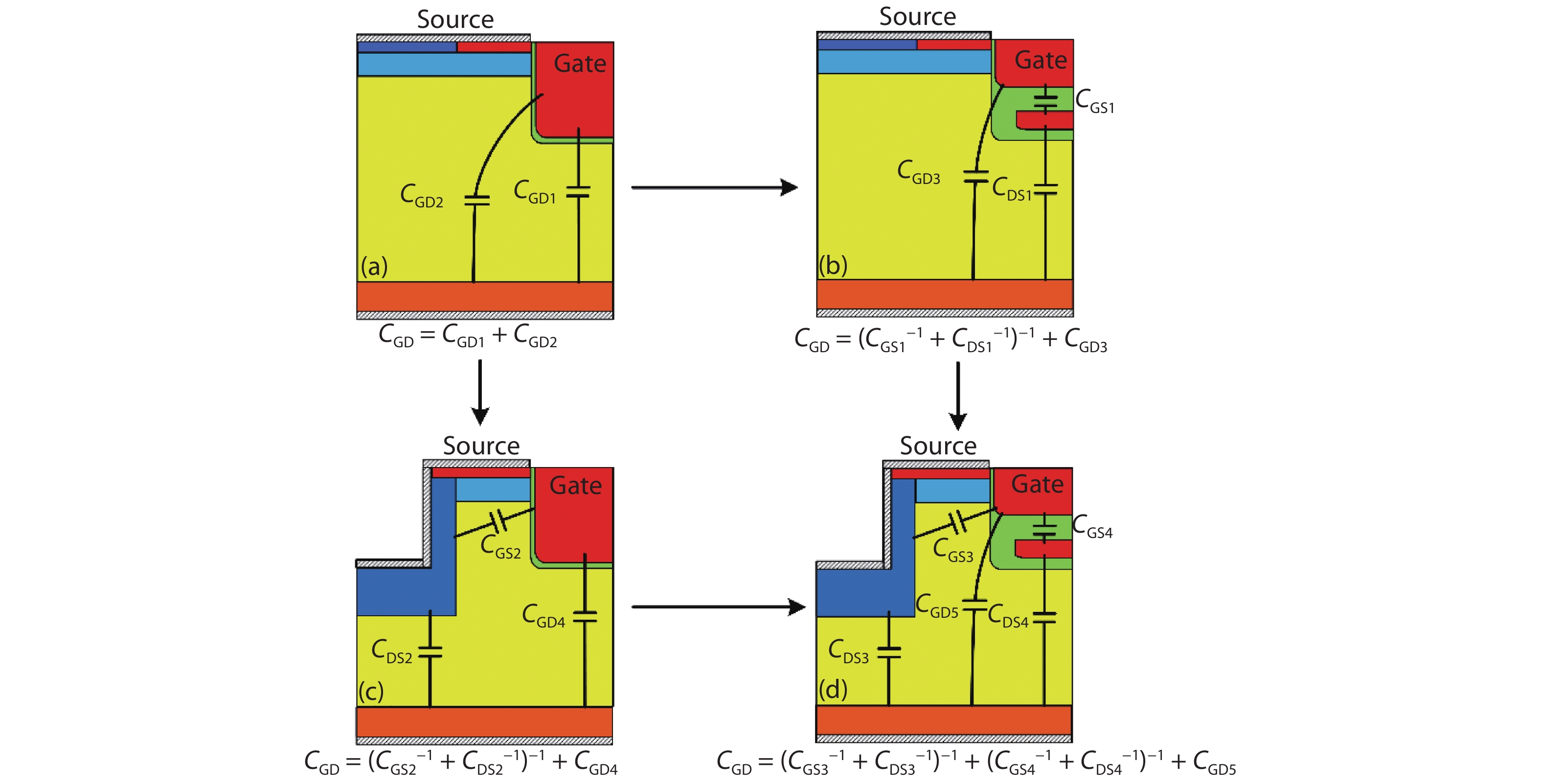
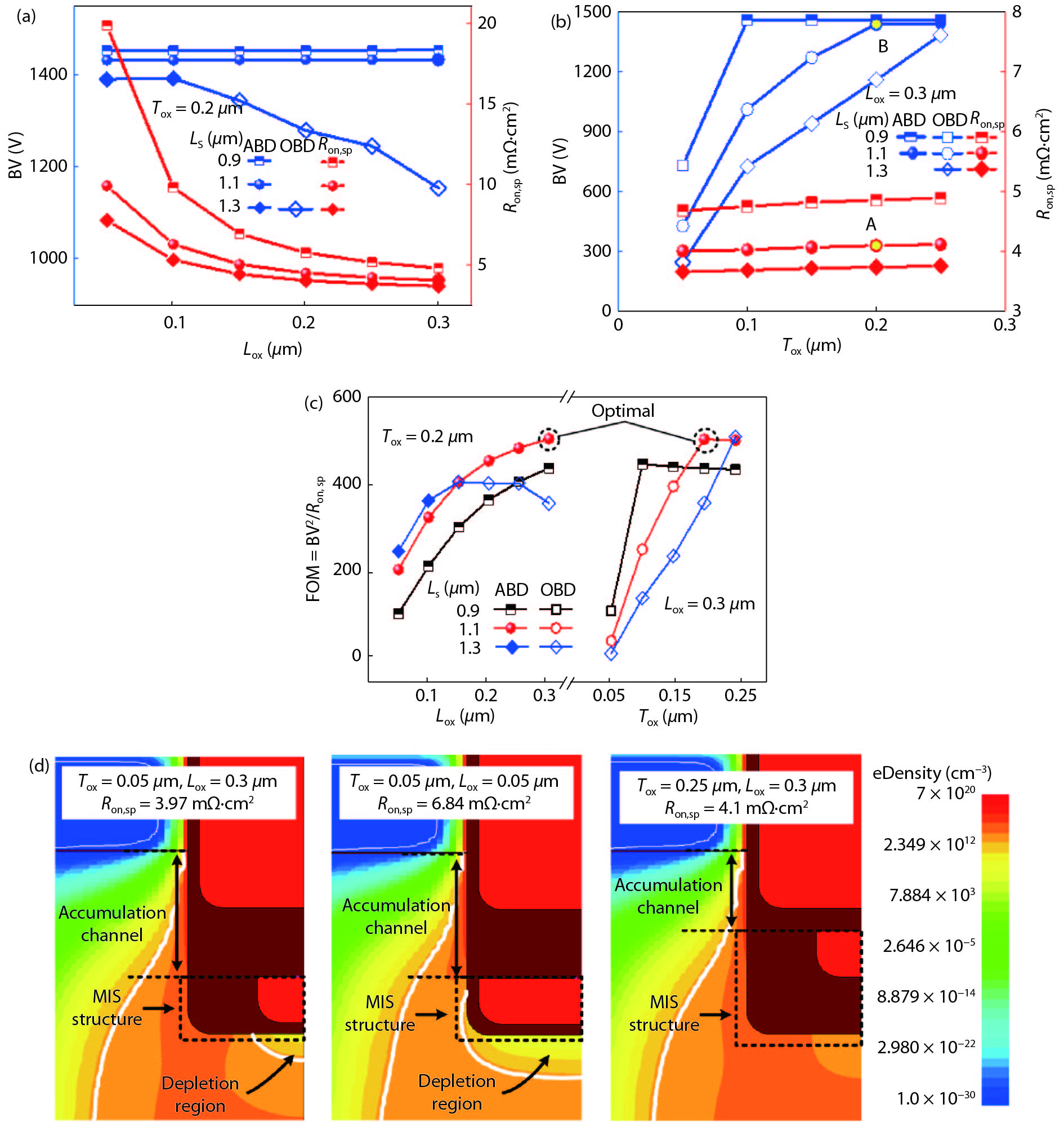
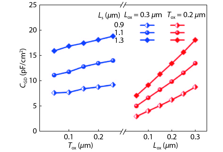
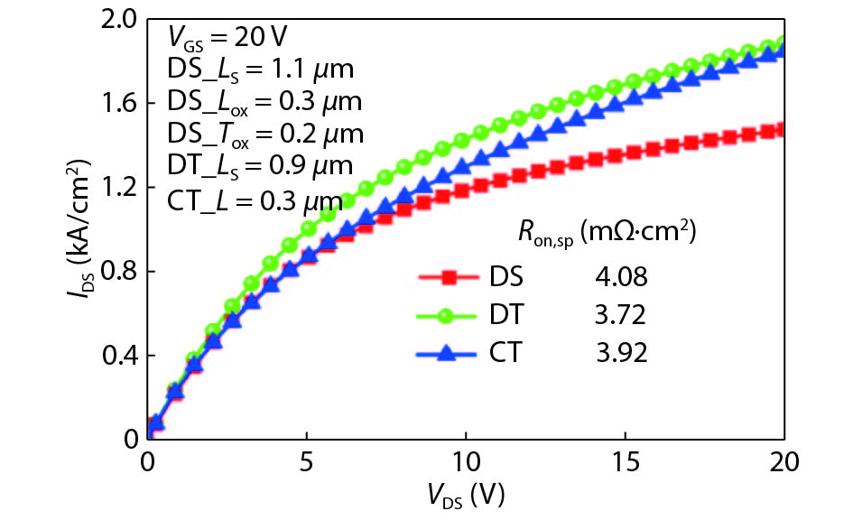

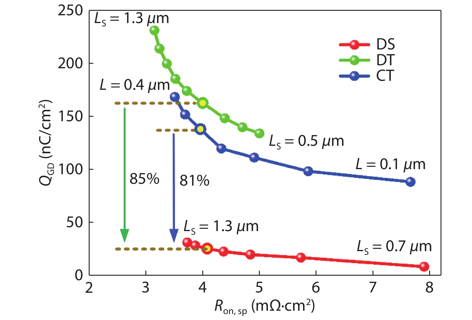
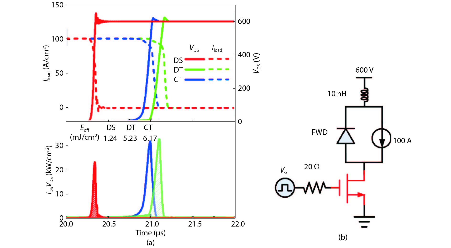
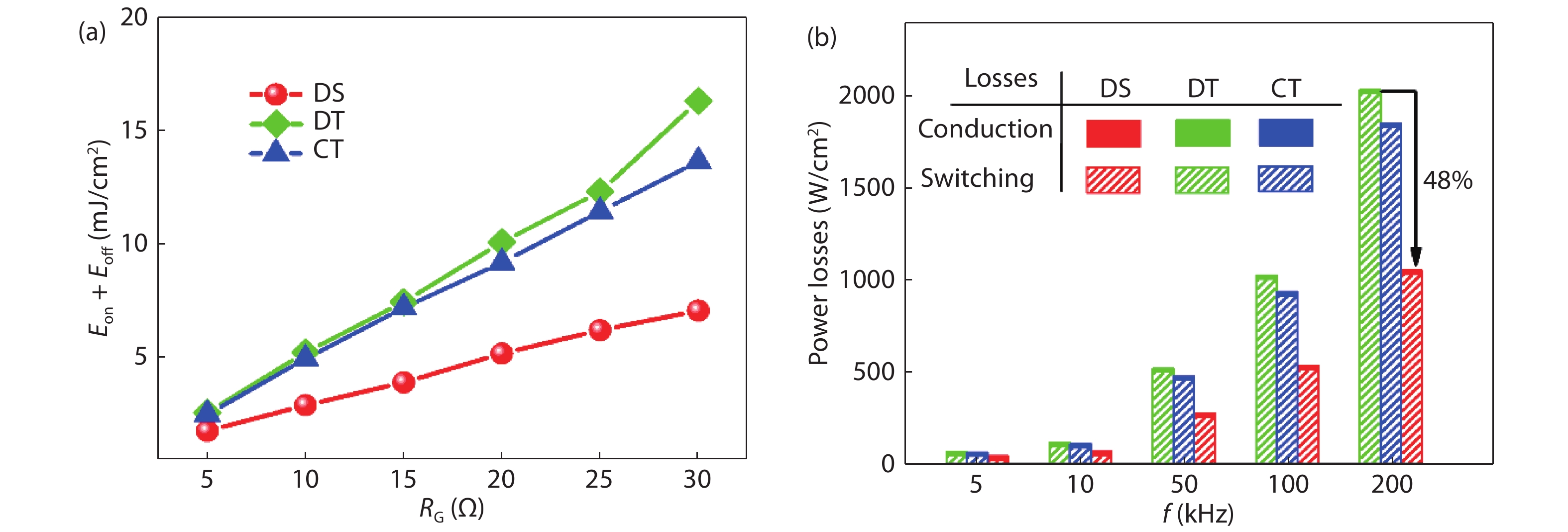
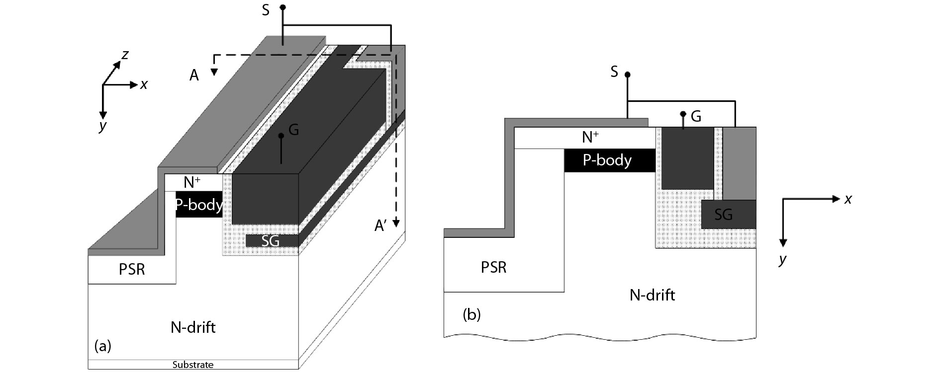
Table 1. Simulation parameters of the proposed structure and contrastive structures.
| Symbol | Description | Value (μm) |
| Dp | Vertical implantation depth of the PSR | 1.5 |
| Wp | Later implantation width of the PSR | 0.2 |
| Dt | Depth of the trench | 1.5 |
| TSG | Thickness of split gate | 0.2 |
| W | Width of half cell | 3.5 |
| Wt | Width of half trench | 0.5 |
 DownLoad: CSV
Table 2. Performance comparison of the three MOSFETs.
| Parameter | DS-MOS | DT-MOS | CT-MOS |
| dV/dt (kV/μs) | 16.1 | 4.7 | 5.5 |
| dI/dt (kA/μs) | 2.6 | 2.2 | 1.6 |
| QGD (nC/cm2) | 26 | 174 | 138 |
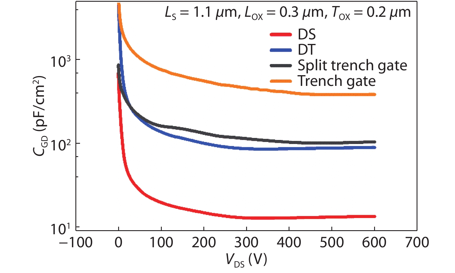
| CGD (pF/cm2) (@VDS = 600 V) | 13 | 68 | 83 |
| Ron, sp (mΩ·cm2) | 4.08 | 3.72 | 3.96 |
| Ron, spQGD (mΩ·nC) | 106 | 647 | 546 |
| VBR (V) | 1435 | 1460 | 1233 |
DownLoad: CSV
| [1] |
Pittini R, Zhang Z, Andersen M A E. Switching performance evaluation of commercial SiC power devices (SiC JFET and SiC MOSFET) in relation to the gate driver complexity. IEEE ECCE Asia Downunder, 2013, 233
|
| [2] |
Zhang X, Yao C, Li C, et al. A wide bandgap device-based isolated quasi-switched-capacitor DC/DC converter. IEEE Trans Power Electron, 2014, 29(5), 2500 doi: 10.1109/TPEL.2013.2287501
|
| [3] |
Abbatelli L, Macauda M, Catalisano G, et al. Cost benefits on high frequency converter system based on SiC MOSFET approach. PCIM Europe; International Exhibition and Conference for Power Electronics, Intelligent Motion, Renewable Energy and Energy Management, 2014, 1
|
| [4] |
T Kimoto, J A Cooper. Fundamentals of silicon carbide technology: growth, characterization, devices, and applications. Singapore: Wiley, 2014
|
| [5] |
Tega N, Hisamoto D, Shima A, et al. Channel properties of SiC trench-etched double-implanted MOS (TED MOS). IEEE Trans Electron Devices, 2016, 63(9), 1 doi: 10.1109/ted.2016.2587799
|
| [6] |
Zhang Q, Gomez M. 1600V 4H-SiC UMOSFETs with dual buffer layers. International Symposium on Power Semiconductor Devices and ICs, 2005, 211
|
| [7] |
Sui Y, Tsuji T, Cooper J A. On-state characteristics of SiC power UMOSFETs on 115-μm drift layers. IEEE Electron Device Lett, 2005, 26(4), 255 doi: 10.1109/LED.2005.845495
|
| [8] |
Tega N, Yoshimoto H,Hisamoto D, et al. Novel trench-etched double-diffused SiC MOS (TED MOS) for overcoming tradeoff between RonA and Qgd. International Symposium on Power Semiconductor Devices and ICs, 2015, 81
|
| [9] |
Cooper J A, Melloch M R, Singh R, et al. Status and prospects for SiC power MOSFETs. IEEE Trans Electron Devices, 2002, 49(4), 658 doi: 10.1109/16.992876
|
| [10] |
Hiroshi Y, Hatayama N H. Increased channel mobility in 4H-SiC UMOSFETs using on-axis substrates. Mater Sci Forum, 2007, 556/557, 807 doi: 10.4028/www.scientific.net/MSF.556-557
|
| [11] |
Tan J, Cooper J A, Melloch M R. High-voltage accumulation-layer UMOSFET’s in 4H-SiC. IEEE Electron Device Lett, 1998, 19(12), 487 doi: 10.1109/55.735755
|
| [12] |
Kagawa Y, Fujiwara N, Sugawara K, et al. 4H-SiC trench MOSFET with bottom oxide protection. Mater Sci Forum, 2014, 778–780, 907 doi: 10.4028/www.scientific.net/MSF.778-780
|
| [13] |
Wang Y, Ma Y C, Hao Y, et al. Simulation study of 4H-SiC UMOSFET structure with p+-polySi/SiC shielded region. IEEE Trans Electron Devices, 2017, 64(9) doi: 10.1109/TED.2017.2723502
|
| [14] |
Wei J, Zhang M, Jiang H, et al. Charge storage effect in SiC trench MOSFET with a floating p-shield and its impact on dynamic performances. International Symposium on Power Semiconductor Devices and ICs, 2017, 387
|
| [15] |
Khan I A, Cooper J A, Capano M A, et al. High-voltage UMOSFETs in 4H SiC. International Symposium on Power Semiconductor Devices and ICs, 2002, 157
|
| [16] |
Wei J, Zhang M, Jiang H P, et al. Dynamic degradation in SiC trench MOSFET with a floating p-shield revealed with numerical simulations. IEEE Trans Electron Devices, 2017, 64(4), 2592 doi: 10.1109/TED.2017.2697763
|
| [17] |
Nakamura T, Nakano Y, Aketa M, et al. Performance SiC trench devices with ultra-low Ron. Electron Devices Meeting, 2011, 26.5.1
|
| [18] |
Goarin P, Koops G E J, Dalen R V, et al. Split-gate resurf stepped oxide (RSO) MOSFETs for 25 V applications with record low gate-to-drain charge. International Symposium on Power Semiconductor Devices and ICs, 2007, 61
|
| [19] |
Luo X, Ma D, Tan Q, et al. A split gate power FINFET with improved ON-resistance and switching performance. IEEE Electron Device Lett, 2016, 37(9), 1185 doi: 10.1109/LED.2016.2591780
|
| [20] |
Zhou X, Yue R, Zhang J, et al. 4H-SiC trench MOSFET with floating/grounded junction barrier-controlled gate structure. IEEE Trans Electron Devices, 2017, 64(11), 4568 doi: 10.1109/TED.2017.2755721
|
| [21] |
J Lutz, U Scheuermann, H Schlangenotto, et al. Semiconductor power devices: physics, characteristics, reliability. New York: Spring-Verlag, 2011
|


Article views: 5710 Times PDF downloads: 320 Times Cited by: 0 Times
Received: 07 January 2019 Revised: 25 March 2019 Online: Accepted Manuscript: 20 April 2019Uncorrected proof: 24 April 2019Published: 08 May 2019
| Citation: |
Xiaorong Luo, Tian Liao, Jie Wei, Jian Fang, Fei Yang, Bo Zhang. A novel 4H-SiC trench MOSFET with double shielding structures and ultralow gate-drain charge[J]. Journal of Semiconductors, 2019, 40(5): 052803. doi: 10.1088/1674-4926/40/5/052803
****
X R Luo, T Liao, J Wei, J Fang, F Yang, B Zhang, A novel 4H-SiC trench MOSFET with double shielding structures and ultralow gate-drain charge[J]. J. Semicond., 2019, 40(5): 052803. doi: 10.1088/1674-4926/40/5/052803.

|
| [1] |
Pittini R, Zhang Z, Andersen M A E. Switching performance evaluation of commercial SiC power devices (SiC JFET and SiC MOSFET) in relation to the gate driver complexity. IEEE ECCE Asia Downunder, 2013, 233
|
| [2] |
Zhang X, Yao C, Li C, et al. A wide bandgap device-based isolated quasi-switched-capacitor DC/DC converter. IEEE Trans Power Electron, 2014, 29(5), 2500 doi: 10.1109/TPEL.2013.2287501
|
| [3] |
Abbatelli L, Macauda M, Catalisano G, et al. Cost benefits on high frequency converter system based on SiC MOSFET approach. PCIM Europe; International Exhibition and Conference for Power Electronics, Intelligent Motion, Renewable Energy and Energy Management, 2014, 1
|
| [4] |
T Kimoto, J A Cooper. Fundamentals of silicon carbide technology: growth, characterization, devices, and applications. Singapore: Wiley, 2014
|
| [5] |
Tega N, Hisamoto D, Shima A, et al. Channel properties of SiC trench-etched double-implanted MOS (TED MOS). IEEE Trans Electron Devices, 2016, 63(9), 1 doi: 10.1109/ted.2016.2587799
|
| [6] |
Zhang Q, Gomez M. 1600V 4H-SiC UMOSFETs with dual buffer layers. International Symposium on Power Semiconductor Devices and ICs, 2005, 211
|
| [7] |
Sui Y, Tsuji T, Cooper J A. On-state characteristics of SiC power UMOSFETs on 115-μm drift layers. IEEE Electron Device Lett, 2005, 26(4), 255 doi: 10.1109/LED.2005.845495
|
| [8] |
Tega N, Yoshimoto H,Hisamoto D, et al. Novel trench-etched double-diffused SiC MOS (TED MOS) for overcoming tradeoff between RonA and Qgd. International Symposium on Power Semiconductor Devices and ICs, 2015, 81
|
| [9] |
Cooper J A, Melloch M R, Singh R, et al. Status and prospects for SiC power MOSFETs. IEEE Trans Electron Devices, 2002, 49(4), 658 doi: 10.1109/16.992876
|
| [10] |
Hiroshi Y, Hatayama N H. Increased channel mobility in 4H-SiC UMOSFETs using on-axis substrates. Mater Sci Forum, 2007, 556/557, 807 doi: 10.4028/www.scientific.net/MSF.556-557
|
| [11] |
Tan J, Cooper J A, Melloch M R. High-voltage accumulation-layer UMOSFET’s in 4H-SiC. IEEE Electron Device Lett, 1998, 19(12), 487 doi: 10.1109/55.735755
|
| [12] |
Kagawa Y, Fujiwara N, Sugawara K, et al. 4H-SiC trench MOSFET with bottom oxide protection. Mater Sci Forum, 2014, 778–780, 907 doi: 10.4028/www.scientific.net/MSF.778-780
|
| [13] |
Wang Y, Ma Y C, Hao Y, et al. Simulation study of 4H-SiC UMOSFET structure with p+-polySi/SiC shielded region. IEEE Trans Electron Devices, 2017, 64(9) doi: 10.1109/TED.2017.2723502
|
| [14] |
Wei J, Zhang M, Jiang H, et al. Charge storage effect in SiC trench MOSFET with a floating p-shield and its impact on dynamic performances. International Symposium on Power Semiconductor Devices and ICs, 2017, 387
|
| [15] |
Khan I A, Cooper J A, Capano M A, et al. High-voltage UMOSFETs in 4H SiC. International Symposium on Power Semiconductor Devices and ICs, 2002, 157
|
| [16] |
Wei J, Zhang M, Jiang H P, et al. Dynamic degradation in SiC trench MOSFET with a floating p-shield revealed with numerical simulations. IEEE Trans Electron Devices, 2017, 64(4), 2592 doi: 10.1109/TED.2017.2697763
|
| [17] |
Nakamura T, Nakano Y, Aketa M, et al. Performance SiC trench devices with ultra-low Ron. Electron Devices Meeting, 2011, 26.5.1
|
| [18] |
Goarin P, Koops G E J, Dalen R V, et al. Split-gate resurf stepped oxide (RSO) MOSFETs for 25 V applications with record low gate-to-drain charge. International Symposium on Power Semiconductor Devices and ICs, 2007, 61
|
| [19] |
Luo X, Ma D, Tan Q, et al. A split gate power FINFET with improved ON-resistance and switching performance. IEEE Electron Device Lett, 2016, 37(9), 1185 doi: 10.1109/LED.2016.2591780
|
| [20] |
Zhou X, Yue R, Zhang J, et al. 4H-SiC trench MOSFET with floating/grounded junction barrier-controlled gate structure. IEEE Trans Electron Devices, 2017, 64(11), 4568 doi: 10.1109/TED.2017.2755721
|
| [21] |
J Lutz, U Scheuermann, H Schlangenotto, et al. Semiconductor power devices: physics, characteristics, reliability. New York: Spring-Verlag, 2011
|

 WeChat ID
Journal of Semiconductors © 2017 All Rights Reserved 京ICP备05085259号-2