


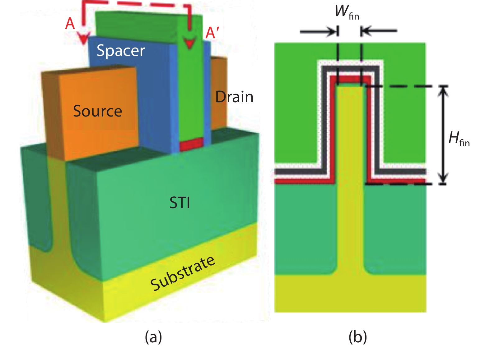
Fig. 1.
(Color online) The structure diagram of nFinFET. (a) A 3D model of bulk FinFET. (b) A cross-section view along A–A’ direction[13].
ARTICLES
Baoshun Wang1, 2, Jiangwei Cui1, 2, , Qi Guo1, 2, Qiwen Zheng1, 2, Ying Wei1, 2 and Shanxue Xi1, 2
Corresponding author: Jiangwei Cui, cuijw@ms.xjb.ac.cn
Abstract: We investigate the hot carrier injection effect (HCI) and how X-ray radiation impacts the HCI of 22-nm nFinFETs as a function of device geometry and irradiation bias conditions in this paper. In the HCI test, the degradation of threshold voltage and saturation current decreases with the increase of fin number, which means that HCI weakens when the fin number increases. The reason is attributed to the coupling effect between fins. Moreover, irradiation is shown to weaken the degradation during the subsequent hot carrier test. The influence of irradiation on HCI is more obvious with ON bias than that of OFF bias and transmission gate bias. It is supposed that the Si–H bonds can be broken by irradiation before the HCI test, which is one reason for the irradiation influence on HCI. Besides, trapped charges are generated in the shallow trench isolation by the radiation, which could reduce the channel electric field, and then weaken the HCI.
| [1] |
Zhang E X, Fleetwood D M, Hachtel J A, et al. Total ionizing dose effects on strained Ge pMOS FinFETs on bulk Si. IEEE Trans Nucl Sci, 2017, 64, 226 doi: 10.1109/TNS.2016.2635023
|
| [2] |
Chatterjee I, Zhang E X, Bhuva B L, et al. Bias dependence of total-dose effects in bulk FinFETs. IEEE Trans Nucl Sci, 2013, 60, 4476 doi: 10.1109/TNS.2013.2287872
|
| [3] |
Chung E A, Nam K J, Nakanishi T, et al. Investigation of hot carrier degradation in bulk FinFET. 2017 IEEE International Reliability Physics Symposium, 2017
|
| [4] |
Chang W T, Cin L G, Yeh W K. Impact of fin width and back bias under hot carrier injection on double-gate FinFETs. IEEE Trans Device Mater Reliab, 2015, 15, 86 doi: 10.1109/TDMR.2014.2384737
|
| [5] |
Ma C Y, Li B, Wei Y Q, et al. FinFET reliability study by forward gated-diode method. 2008 9th International Conference on Solid-State and Integrated-Circuit Technology, 2008, 644
|
| [6] |
Jiang H, Yin L X, Li Y, et al. Comprehensive understanding of hot carrier degradation in multiple-fin SOI FinFETs. 2015 IEEE International Reliability Physics Symposium, 2015
|
| [7] |
Yeh W K, Chen P Y, Shih C H, et al. The impact of fin number on device's performance and reliability in tri-gate FinFETs. 2017 IEEE Electron Devices Technology and Manufacturing Conference (EDTM), 2017
|
| [8] |
Tang X Y, Lu J W, Zhang R, et al. Positive bias temperature instability and hot carrier injection of back gate ultra-thin-body In0.53Ga0.47As-on-insulator n-channel metal–oxide–semiconductor field-effect transistor. Chin Phys Lett, 2015, 32, 117302 doi: 10.1088/0256-307X/32/11/117302
|
| [9] |
Silvestri M, Gerardin S, Paccagnella A, et al. Channel hot carrier stress on irradiated 130-nm NMOSFETs: Impact of bias conditions during X-ray exposure. 2007 9th European Conference on Radiation and Its Effects on Components and Systems, 2007, 1
|
| [10] |
Zheng Q W, Cui J W, Zhou H, et al. Hot-carrier effects on total dose irradiated 65 nm n-type metal–oxide–semiconductor field-effect transistors. Chin Phys Lett, 2016, 33, 076102 doi: 10.1088/0256-307X/33/7/076102
|
| [11] |
Cui J W, Zheng Q W, Ning B X, et al. Hot-carrier effect on TID irradiated short-channel UTTB FD-SOI n-MOSFETs. IEEE Radiation Effects Data Workshop, 2018
|
| [12] |
Das N C, Nathan V, Dacus S, et al. Combined effects of hot-carrier stressing and ionizing radiation in SiO2, NO, and ONO MOSFETs. IEEE Electron Device Lett, 1993, 14, 40 doi: 10.1109/55.215093
|
| [13] |
Yang L, Zhang Q Z, Huang Y B, et al. Total ionizing dose response and annealing behavior of bulk nFinFETs with ON-state bias irradiaiton. IEEE Trans Nucl Sci, 2018, 65, 1503 doi: 10.1109/TNS.2018.2827675
|
| [14] |
Chen Z, Ong P. Direct evidence for multiple vibrational excitationof Si-H/D bonds for hot-carrier degradation of MOS transistors.60th DRC Conference Digest Device Research Conference,2002
|
| [15] |
Zhang H, Jiang H, Fan X, et al. Effects of total-ionizing-dose irradiation on single-event response for flip-flop designs at 14-/16-nm bulk FinFET technology node. IEEE Trans Nucl Sci, 2018, 65, 1928 doi: 10.1109/TNS.2017.2781622
|
| [16] |
King M P, Wu X, Eller M, et al. Analysis of TID process, geometry, and bias condition dependence in 14-nm FinFETs and implications for RF and SRAM performance. IEEE Trans Nucl Sci, 2017, 64, 285 doi: 10.1109/TNS.2016.2634538
|
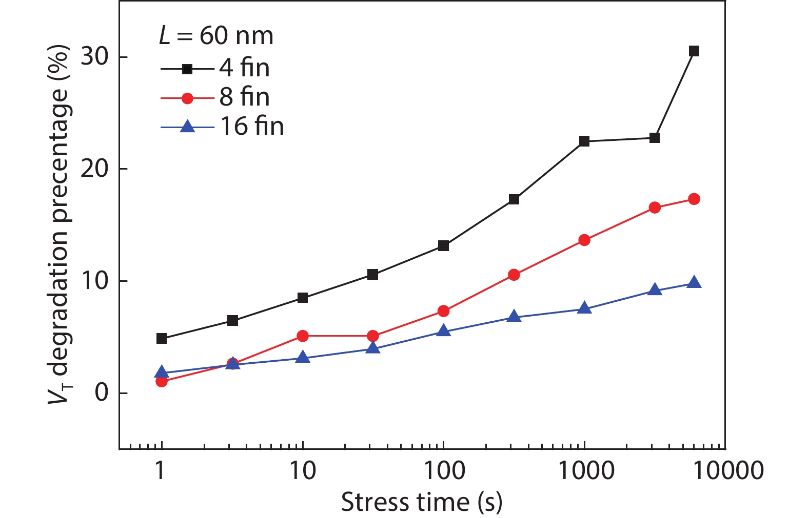
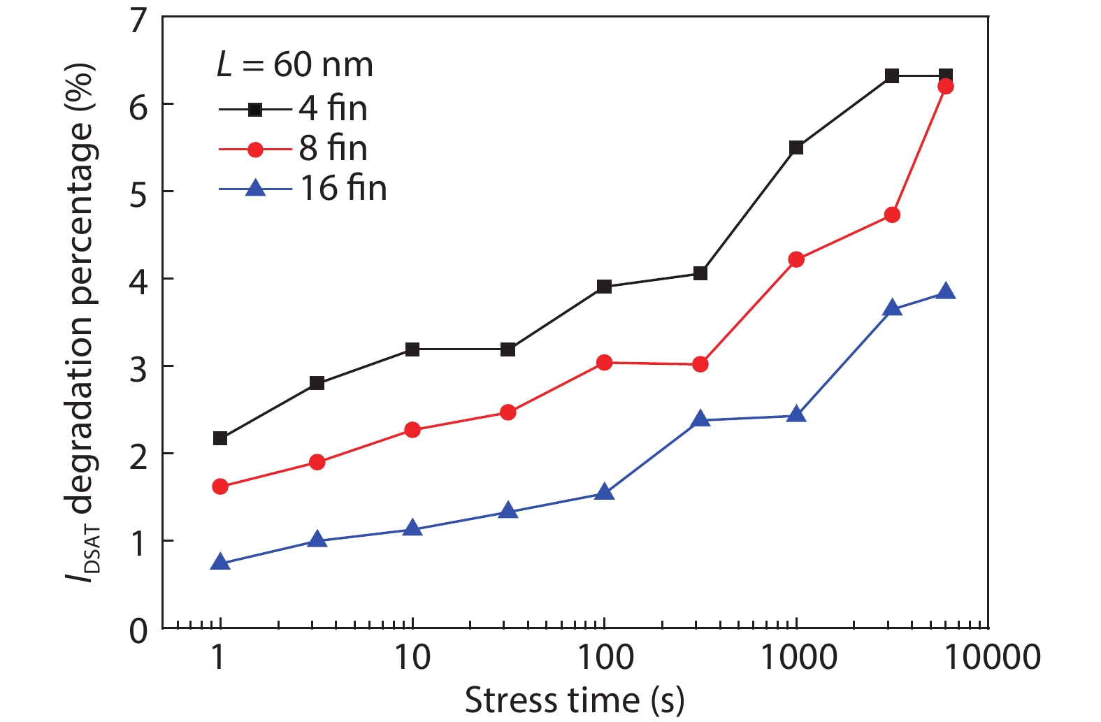
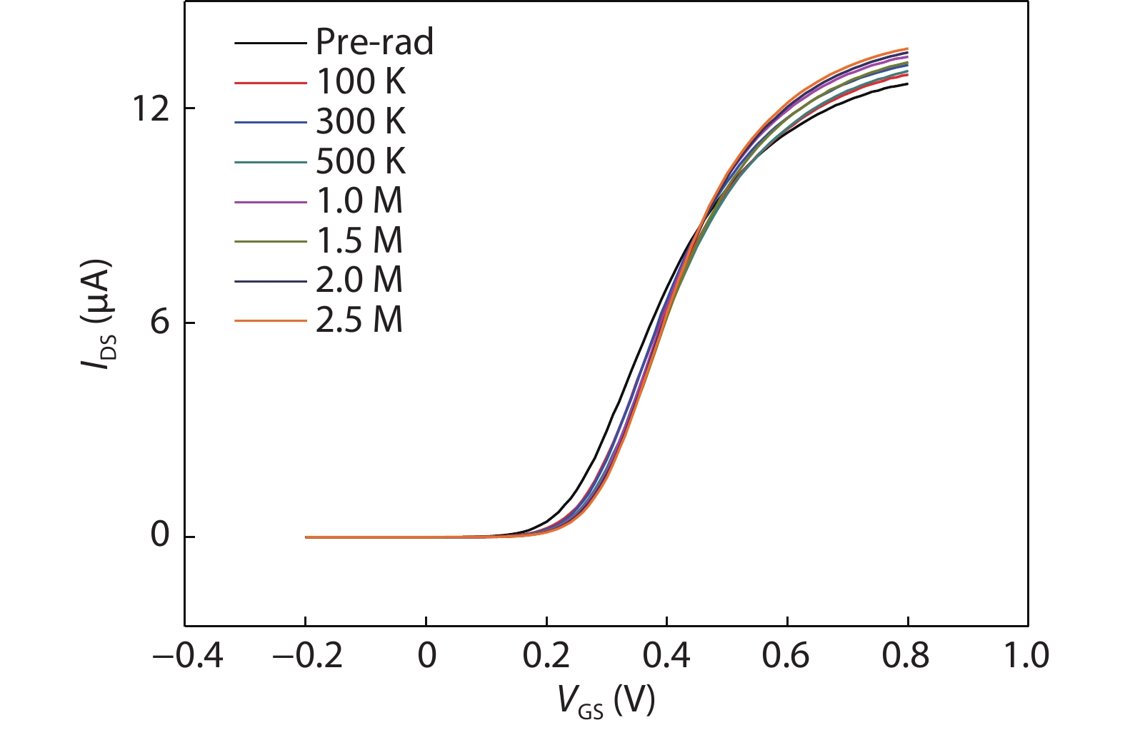
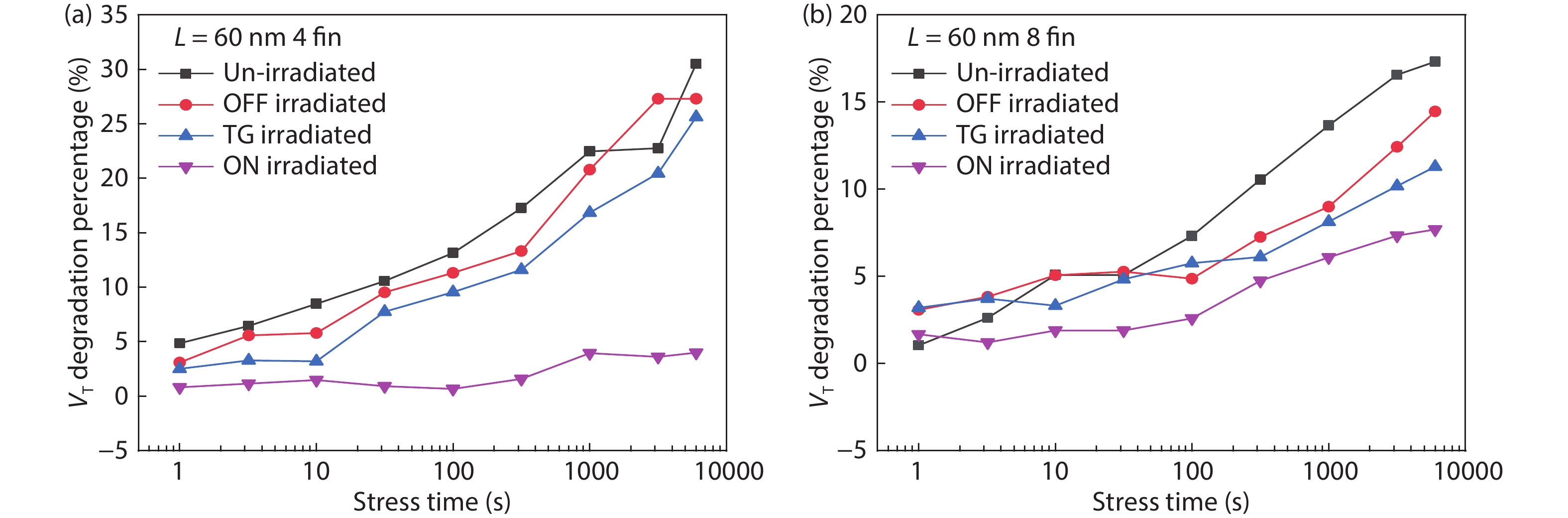
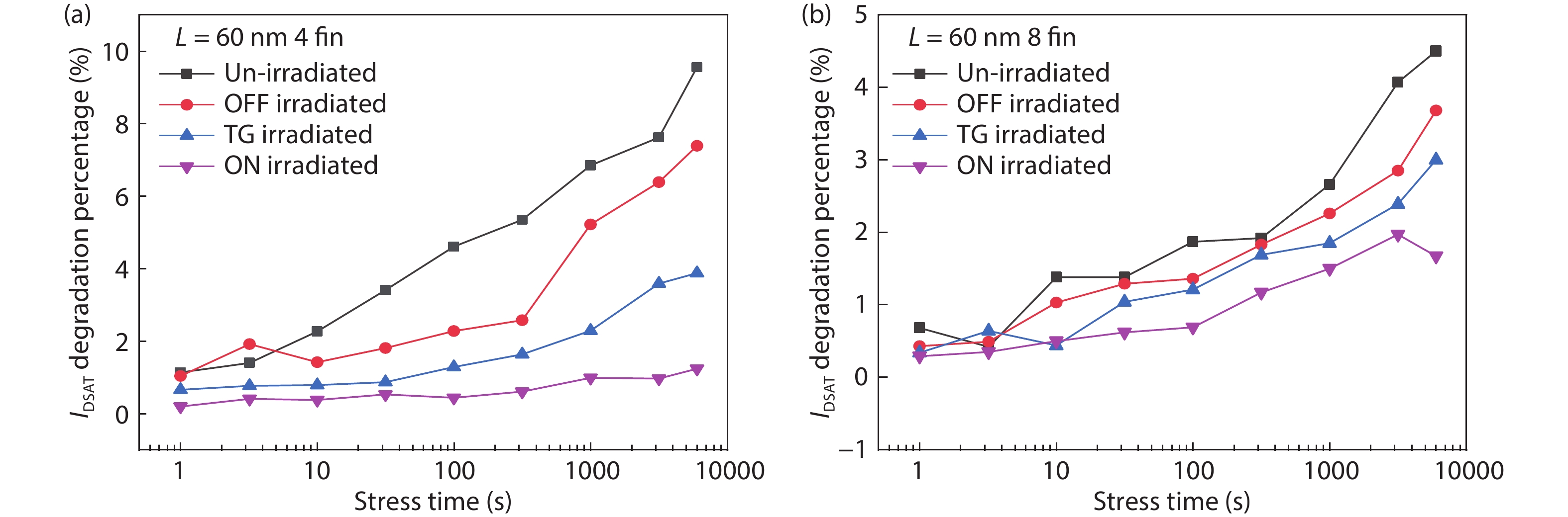
Table 1. VT degradation percentage of un-irradiated devices, OFF-bias irradiated devices, TG-bias irradiated devices, and ON-bias irradiated devices in different groups after 6000 s hot carrier stress.
| Device | Un-irradiated | OFF irradiated | TG irradiated | ON irradiated |
| Lgate = 60 nm, 4 fin | 30.15% | 27.31% | 25.63% | 4.00% |
| Lgate = 60 nm, 8 fin | 17.32% | 14.46% | 11.29% | 7.69% |
 DownLoad: CSV
Table 2. IDSAT degradation percentage of un-irradiated devices, OFF-bias irradiated devices, TG-bias irradiated devices, and ON-bias irradiated devices in different groups after 6000 s hot carrier stress.
| Device | Un-irradiated | OFF irradiated | TG irradiated | ON irradiated |
| Lgate = 60 nm, 4 fin | 9.56% | 7.39% | 3.88% | 1.24% |
| Lgate = 60 nm, 8 fin | 4.5% | 3.68% | 3% | 1.67% |
DownLoad: CSV
| [1] |
Zhang E X, Fleetwood D M, Hachtel J A, et al. Total ionizing dose effects on strained Ge pMOS FinFETs on bulk Si. IEEE Trans Nucl Sci, 2017, 64, 226 doi: 10.1109/TNS.2016.2635023
|
| [2] |
Chatterjee I, Zhang E X, Bhuva B L, et al. Bias dependence of total-dose effects in bulk FinFETs. IEEE Trans Nucl Sci, 2013, 60, 4476 doi: 10.1109/TNS.2013.2287872
|
| [3] |
Chung E A, Nam K J, Nakanishi T, et al. Investigation of hot carrier degradation in bulk FinFET. 2017 IEEE International Reliability Physics Symposium, 2017
|
| [4] |
Chang W T, Cin L G, Yeh W K. Impact of fin width and back bias under hot carrier injection on double-gate FinFETs. IEEE Trans Device Mater Reliab, 2015, 15, 86 doi: 10.1109/TDMR.2014.2384737
|
| [5] |
Ma C Y, Li B, Wei Y Q, et al. FinFET reliability study by forward gated-diode method. 2008 9th International Conference on Solid-State and Integrated-Circuit Technology, 2008, 644
|
| [6] |
Jiang H, Yin L X, Li Y, et al. Comprehensive understanding of hot carrier degradation in multiple-fin SOI FinFETs. 2015 IEEE International Reliability Physics Symposium, 2015
|
| [7] |
Yeh W K, Chen P Y, Shih C H, et al. The impact of fin number on device's performance and reliability in tri-gate FinFETs. 2017 IEEE Electron Devices Technology and Manufacturing Conference (EDTM), 2017
|
| [8] |
Tang X Y, Lu J W, Zhang R, et al. Positive bias temperature instability and hot carrier injection of back gate ultra-thin-body In0.53Ga0.47As-on-insulator n-channel metal–oxide–semiconductor field-effect transistor. Chin Phys Lett, 2015, 32, 117302 doi: 10.1088/0256-307X/32/11/117302
|
| [9] |
Silvestri M, Gerardin S, Paccagnella A, et al. Channel hot carrier stress on irradiated 130-nm NMOSFETs: Impact of bias conditions during X-ray exposure. 2007 9th European Conference on Radiation and Its Effects on Components and Systems, 2007, 1
|
| [10] |
Zheng Q W, Cui J W, Zhou H, et al. Hot-carrier effects on total dose irradiated 65 nm n-type metal–oxide–semiconductor field-effect transistors. Chin Phys Lett, 2016, 33, 076102 doi: 10.1088/0256-307X/33/7/076102
|
| [11] |
Cui J W, Zheng Q W, Ning B X, et al. Hot-carrier effect on TID irradiated short-channel UTTB FD-SOI n-MOSFETs. IEEE Radiation Effects Data Workshop, 2018
|
| [12] |
Das N C, Nathan V, Dacus S, et al. Combined effects of hot-carrier stressing and ionizing radiation in SiO2, NO, and ONO MOSFETs. IEEE Electron Device Lett, 1993, 14, 40 doi: 10.1109/55.215093
|
| [13] |
Yang L, Zhang Q Z, Huang Y B, et al. Total ionizing dose response and annealing behavior of bulk nFinFETs with ON-state bias irradiaiton. IEEE Trans Nucl Sci, 2018, 65, 1503 doi: 10.1109/TNS.2018.2827675
|
| [14] |
Chen Z, Ong P. Direct evidence for multiple vibrational excitationof Si-H/D bonds for hot-carrier degradation of MOS transistors.60th DRC Conference Digest Device Research Conference,2002
|
| [15] |
Zhang H, Jiang H, Fan X, et al. Effects of total-ionizing-dose irradiation on single-event response for flip-flop designs at 14-/16-nm bulk FinFET technology node. IEEE Trans Nucl Sci, 2018, 65, 1928 doi: 10.1109/TNS.2017.2781622
|
| [16] |
King M P, Wu X, Eller M, et al. Analysis of TID process, geometry, and bias condition dependence in 14-nm FinFETs and implications for RF and SRAM performance. IEEE Trans Nucl Sci, 2017, 64, 285 doi: 10.1109/TNS.2016.2634538
|


Article views: 5215 Times PDF downloads: 143 Times Cited by: 0 Times
Received: 07 March 2020 Revised: 17 June 2020 Online: Accepted Manuscript: 06 August 2020Uncorrected proof: 13 August 2020Published: 08 December 2020
| Citation: |
Baoshun Wang, Jiangwei Cui, Qi Guo, Qiwen Zheng, Ying Wei, Shanxue Xi. The influence of total ionizing dose on the hot carrier injection of 22 nm bulk nFinFET[J]. Journal of Semiconductors, 2020, 41(12): 122102. doi: 10.1088/1674-4926/41/12/122102
****
B S Wang, J W Cui, Q Guo, Q W Zheng, Y Wei, S X Xi, The influence of total ionizing dose on the hot carrier injection of 22 nm bulk nFinFET[J]. J. Semicond., 2020, 41(12): 122102. doi: 10.1088/1674-4926/41/12/122102.

|
| [1] |
Zhang E X, Fleetwood D M, Hachtel J A, et al. Total ionizing dose effects on strained Ge pMOS FinFETs on bulk Si. IEEE Trans Nucl Sci, 2017, 64, 226 doi: 10.1109/TNS.2016.2635023
|
| [2] |
Chatterjee I, Zhang E X, Bhuva B L, et al. Bias dependence of total-dose effects in bulk FinFETs. IEEE Trans Nucl Sci, 2013, 60, 4476 doi: 10.1109/TNS.2013.2287872
|
| [3] |
Chung E A, Nam K J, Nakanishi T, et al. Investigation of hot carrier degradation in bulk FinFET. 2017 IEEE International Reliability Physics Symposium, 2017
|
| [4] |
Chang W T, Cin L G, Yeh W K. Impact of fin width and back bias under hot carrier injection on double-gate FinFETs. IEEE Trans Device Mater Reliab, 2015, 15, 86 doi: 10.1109/TDMR.2014.2384737
|
| [5] |
Ma C Y, Li B, Wei Y Q, et al. FinFET reliability study by forward gated-diode method. 2008 9th International Conference on Solid-State and Integrated-Circuit Technology, 2008, 644
|
| [6] |
Jiang H, Yin L X, Li Y, et al. Comprehensive understanding of hot carrier degradation in multiple-fin SOI FinFETs. 2015 IEEE International Reliability Physics Symposium, 2015
|
| [7] |
Yeh W K, Chen P Y, Shih C H, et al. The impact of fin number on device's performance and reliability in tri-gate FinFETs. 2017 IEEE Electron Devices Technology and Manufacturing Conference (EDTM), 2017
|
| [8] |
Tang X Y, Lu J W, Zhang R, et al. Positive bias temperature instability and hot carrier injection of back gate ultra-thin-body In0.53Ga0.47As-on-insulator n-channel metal–oxide–semiconductor field-effect transistor. Chin Phys Lett, 2015, 32, 117302 doi: 10.1088/0256-307X/32/11/117302
|
| [9] |
Silvestri M, Gerardin S, Paccagnella A, et al. Channel hot carrier stress on irradiated 130-nm NMOSFETs: Impact of bias conditions during X-ray exposure. 2007 9th European Conference on Radiation and Its Effects on Components and Systems, 2007, 1
|
| [10] |
Zheng Q W, Cui J W, Zhou H, et al. Hot-carrier effects on total dose irradiated 65 nm n-type metal–oxide–semiconductor field-effect transistors. Chin Phys Lett, 2016, 33, 076102 doi: 10.1088/0256-307X/33/7/076102
|
| [11] |
Cui J W, Zheng Q W, Ning B X, et al. Hot-carrier effect on TID irradiated short-channel UTTB FD-SOI n-MOSFETs. IEEE Radiation Effects Data Workshop, 2018
|
| [12] |
Das N C, Nathan V, Dacus S, et al. Combined effects of hot-carrier stressing and ionizing radiation in SiO2, NO, and ONO MOSFETs. IEEE Electron Device Lett, 1993, 14, 40 doi: 10.1109/55.215093
|
| [13] |
Yang L, Zhang Q Z, Huang Y B, et al. Total ionizing dose response and annealing behavior of bulk nFinFETs with ON-state bias irradiaiton. IEEE Trans Nucl Sci, 2018, 65, 1503 doi: 10.1109/TNS.2018.2827675
|
| [14] |
Chen Z, Ong P. Direct evidence for multiple vibrational excitationof Si-H/D bonds for hot-carrier degradation of MOS transistors.60th DRC Conference Digest Device Research Conference,2002
|
| [15] |
Zhang H, Jiang H, Fan X, et al. Effects of total-ionizing-dose irradiation on single-event response for flip-flop designs at 14-/16-nm bulk FinFET technology node. IEEE Trans Nucl Sci, 2018, 65, 1928 doi: 10.1109/TNS.2017.2781622
|
| [16] |
King M P, Wu X, Eller M, et al. Analysis of TID process, geometry, and bias condition dependence in 14-nm FinFETs and implications for RF and SRAM performance. IEEE Trans Nucl Sci, 2017, 64, 285 doi: 10.1109/TNS.2016.2634538
|

 WeChat ID
Journal of Semiconductors © 2017 All Rights Reserved 京ICP备05085259号-2


