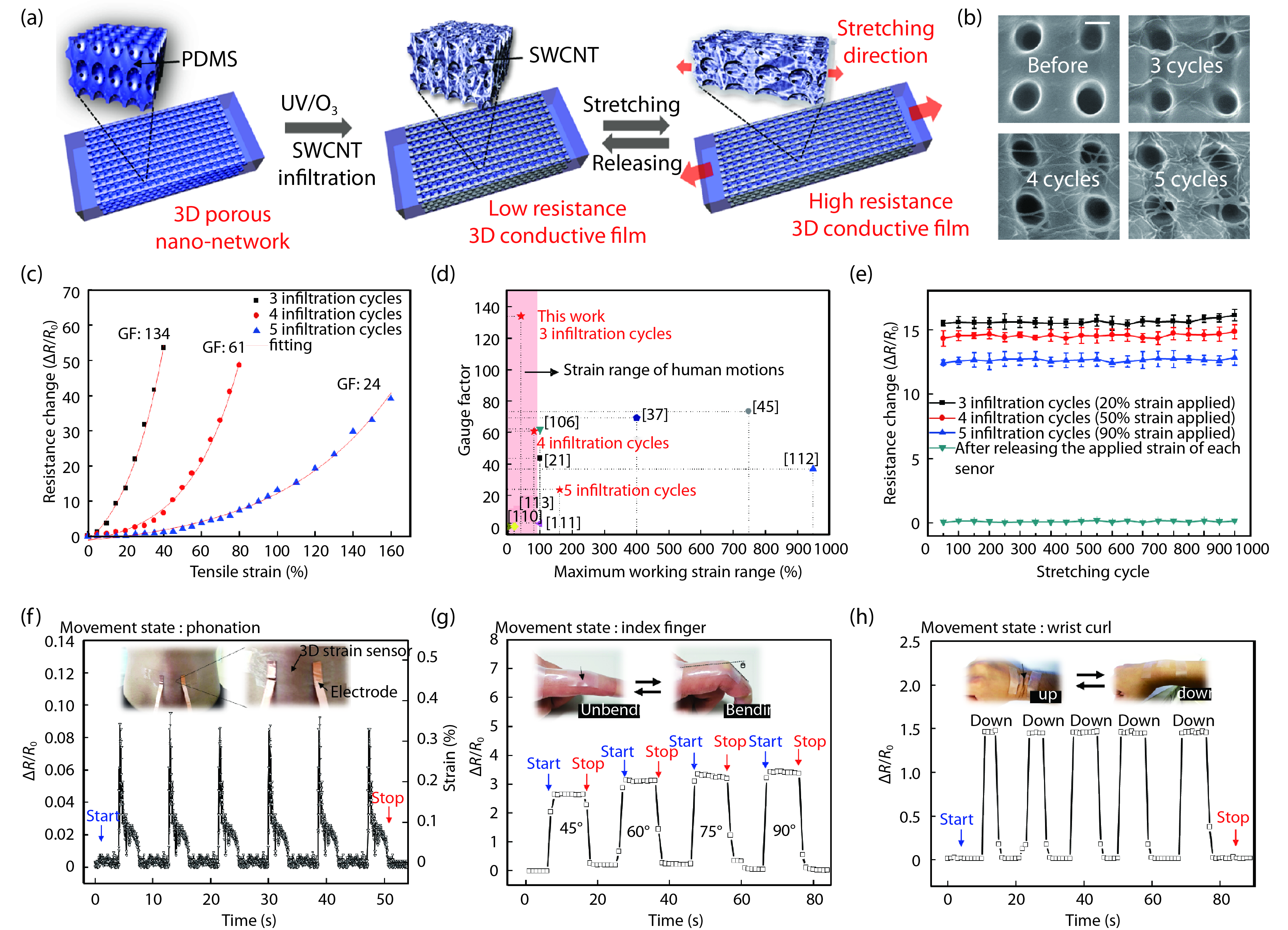
| [1] |
Choi S, Han S I, Kim D, et al. High-performance stretchable conductive nanocomposites: materials, processes, and device applications. Chem Soc Rev, 2019, 48, 1566 doi: 10.1039/C8CS00706C |
| [2] |
Jang K I, Chung H U, Xu S, et al. Soft network composite materials with deterministic and bio-inspired designs. Nat Commun, 2015, 6, 6566 doi: 10.1038/ncomms7566 |
| [3] |
Lin S, Yuk H, Zhang T, et al. Stretchable hydrogel electronics and devices. Adv Mater, 2016, 28, 4497 doi: 10.1002/adma.201504152 |
| [4] |
Liu H, Li Q, Zhang S, et al. Electrically conductive polymer composites for smart flexible strain sensors: a critical review. J Mater Chem C, 2018, 6, 12121 doi: 10.1039/C8TC04079F |
| [5] |
Jeong J, Yeo W H, Akhtar A, et al. Materials and optimized designs for human-machine interfaces via epidermal electronics. Adv Mater, 2013, 25, 6839 doi: 10.1002/adma.201301921 |
| [6] |
Jung S, Kim J, Kim J, et al. Reverse-micelle-induced porous pressure-sensitive rubber for wearable human–machine interfaces. Adv Mater, 2014, 26, 4825 doi: 10.1002/adma.201401364 |
| [7] |
Guo R, Yu Y, Zeng J, et al. Biomimicking topographic elastomeric petals (e-petals) for omnidirectional stretchable and printable electronics. Adv Sci, 2015, 2, 1400021 doi: 10.1002/advs.201400021 |
| [8] |
Kim J, Lee M, Shim H J, et al. Stretchable silicon nanoribbon electronics for skin prosthesis. Nat Commun, 2014, 5, 5747 doi: 10.1038/ncomms6747 |
| [9] |
Lee H, Song C, Hong Y S, et al. Wearable/disposable sweat-based glucose monitoring device with multistage transdermal drug delivery module. Sci Adv, 2017, 3, e1601314 doi: 10.1126/sciadv.1601314 |
| [10] |
Hong S, Lee H, Lee J, et al. Highly stretchable and transparent metal nanowire heater for wearable electronics applications. Adv Mater, 2015, 27, 4744 doi: 10.1002/adma.201500917 |
| [11] |
Lee H, Choi T K, Lee Y B, et al. A graphene-based electrochemical device with thermoresponsive microneedles for diabetes monitoring and therapy. Nat Nanotechnol, 2016, 11, 566 doi: 10.1038/nnano.2016.38 |
| [12] |
Choi M K, Yang J, Kang K, et al. Wearable red–green–blue quantum dot light-emitting diode array using high-resolution intaglio transfer printing. Nat Commun, 2015, 6, 7149 doi: 10.1038/ncomms8149 |
| [13] |
Koo J H, Kim D C, Shim H J, et al. Flexible and stretchable smart display: materials, fabrication, device design, and system integration. Adv Funct Mater, 2018, 28, 1801834 doi: 10.1002/adfm.201801834 |
| [14] |
Li K, Zhang Y, Zhen H, et al. Versatile biomimetic haze films for efficiency enhancement of photovoltaic devices. J Mater Chem A, 2017, 5, 969 doi: 10.1039/C6TA07586J |
| [15] |
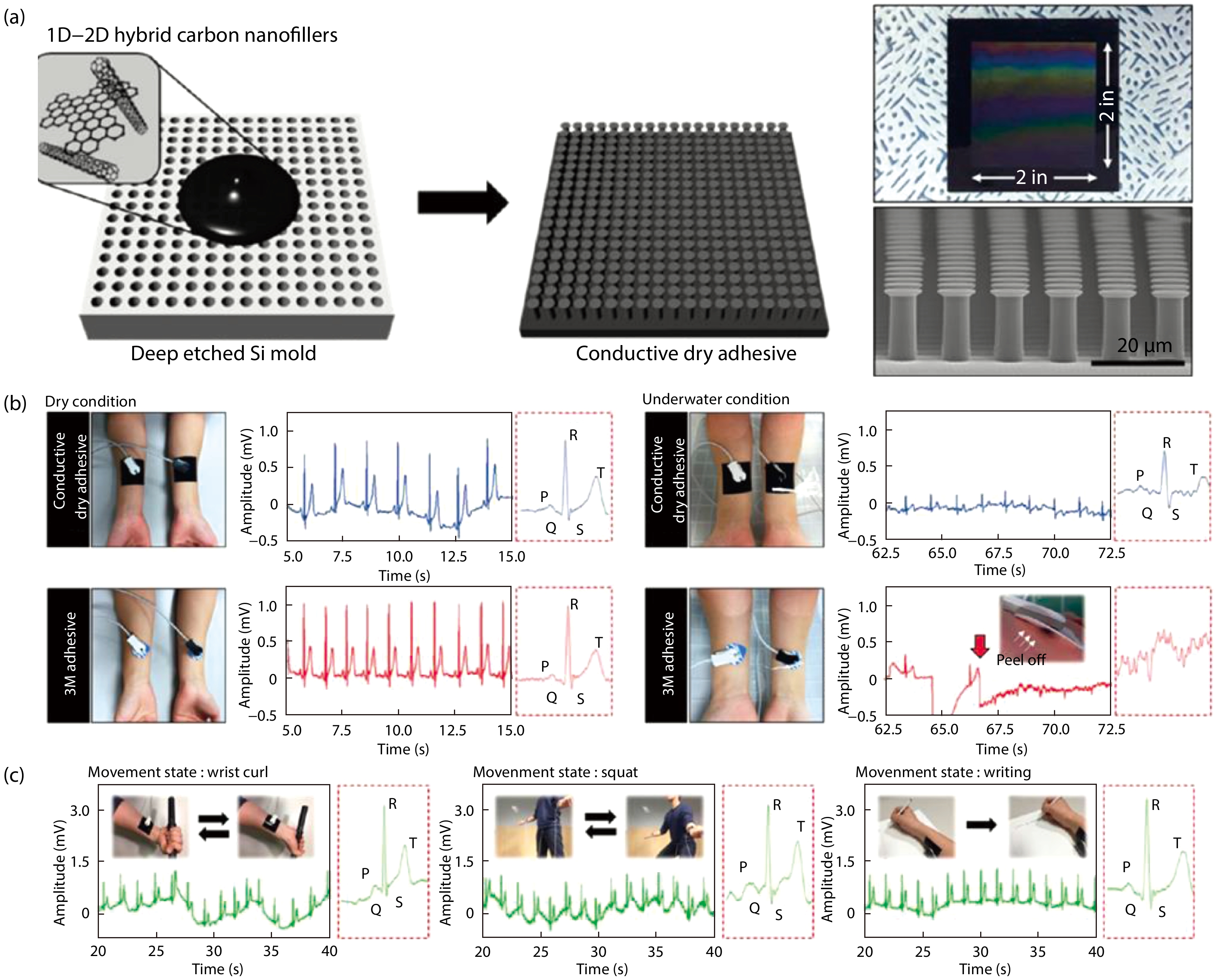
Kim T, Park J, Sohn J, et al. Bioinspired, highly stretchable, and conductive dry adhesives based on 1D–2D hybrid carbon nanocomposites for all-in-one ECG electrodes. ACS Nano, 2016, 10, 4770 doi: 10.1021/acsnano.6b01355 |
| [16] |
Hwang S W, Lee C H, Cheng H, et al. Biodegradable elastomers and silicon nanomembranes/nanoribbons for stretchable, transient electronics, and biosensors. Nano Lett, 2015, 15, 2801 doi: 10.1021/nl503997m |
| [17] |
Yeo W H, Kim Y S, Lee J, et al. Multifunctional epidermal electronics printed directly onto the skin. Adv Mater, 2013, 25, 2773 doi: 10.1002/adma.201204426 |
| [18] |
Son D, Lee J, Qiao S, et al. Multifunctional wearable devices for diagnosis and therapy of movement disorders. Nat Nanotechnol, 2014, 9, 397 doi: 10.1038/nnano.2014.38 |
| [19] |
Park J, Lee Y, Hong J, et al. Giant tunneling piezoresistance of composite elastomers with interlocked microdome arrays for ultrasensitive and multimodal electronic skins. ACS Nano, 2014, 8, 4689 doi: 10.1021/nn500441k |
| [20] |
Park H, Jeong Y R, Yun J, et al. Stretchable array of highly sensitive pressure sensors consisting of polyaniline nanofibers and Au-coated polydimethylsiloxane micropillars. ACS Nano, 2015, 9, 9974 doi: 10.1021/acsnano.5b03510 |
| [21] |
Amjadi M, Pichitpajongkit A, Lee S, et al. Highly stretchable and sensitive strain sensor based on silver nanowire–elastomer nanocomposite. ACS Nano, 2014, 8, 5154 doi: 10.1021/nn501204t |
| [22] |
Hwang B U, Lee J H, Trung T Q, et al. Transparent stretchable self-powered patchable sensor platform with ultrasensitive recognition of human activities. ACS Nano, 2015, 9, 8801 doi: 10.1021/acsnano.5b01835 |
| [23] |
Park J, Wang S, Li M, et al. Three-dimensional nanonetworks for giant stretchability in dielectrics and conductors. Nat Commun, 2012, 3, 916 doi: 10.1038/ncomms1929 |
| [24] |
Cho D, Park J, Kim J, et al. Three-dimensional continuous conductive nanostructure for highly sensitive and stretchable strain sensor. ACS Appl Mater Interfaces, 2017, 9, 17369 doi: 10.1021/acsami.7b03052 |
| [25] |
Yamada T, Hayamizu Y, Yamamoto Y, et al. A stretchable carbon nanotube strain sensor for human-motion detection. Nat Nanotechnol, 2011, 6, 296 doi: 10.1038/nnano.2011.36 |
| [26] |
Lipomi D J, Vosgueritchian M, Tee B C, et al. Skin-like pressure and strain sensors based on transparent elastic films of carbon nanotubes. Nat Nanotechnol, 2011, 6, 788 doi: 10.1038/nnano.2011.184 |
| [27] |
Lu N, Lu C, Yang S, et al. Highly sensitive skin-mountable strain gauges based entirely on elastomers. Adv Funct Mater, 2012, 22, 4044 doi: 10.1002/adfm.201200498 |
| [28] |
Xu S, Yan Z, Jang K I, et al. Assembly of micro/nanomaterials into complex, three-dimensional architectures by compressive buckling. Science, 2015, 347, 154 doi: 10.1126/science.1260960 |
| [29] |
Kim J, Son D, Lee M, et al. A wearable multiplexed silicon nonvolatile memory array using nanocrystal charge confinement. Sci Adv, 2016, 2, e1501101 doi: 10.1126/sciadv.1501101 |
| [30] |
Lee J, Yoo B, Lee H, et al. Ultra-wideband multi-dye-sensitized upconverting nanoparticles for information security application. Adv Mater, 2017, 29, 1603169 doi: 10.1002/adma.201603169 |
| [31] |
Song J K, Son D, Kim J, et al. Wearable force touch sensor array using a flexible and transparent electrode. Adv Funct Mater, 2017, 27, 1605286 doi: 10.1002/adfm.201605286 |
| [32] |
Yan C, Kang W, Wang J, et al. Stretchable and wearable electrochromic devices. ACS Nano, 2013, 8, 316 doi: 10.1021/nn404061g |
| [33] |
Park K, Lee D K, Kim B S, et al. Stretchable, transparent zinc oxide thin film transistors. Adv Funct Mater, 2010, 20, 3577 doi: 10.1002/adfm.201001107 |
| [34] |
Kim D H, Ahn J H, Choi W M, et al. Stretchable and foldable silicon integrated circuits. Science, 2008, 320, 507 doi: 10.1126/science.1154367 |
| [35] |
Kim S Y, Bong J H, Kim C, et al. Mechanical stability analysis via neutral mechanical plane for high-performance flexible si nanomembrane fdsoi device. Adv Mater Interfaces, 2017, 4, 1700618 doi: 10.1002/admi.201700618 |
| [36] |
Kaltenbrunner M, Sekitani T, Reeder J, et al. An ultra-lightweight design for imperceptible plastic electronics. Nature, 2013, 499, 458 doi: 10.1038/nature12314 |
| [37] |
Rogers J A, Someya T, Huang Y. Materials and mechanics for stretchable electronics. Science, 2010, 327, 1603 doi: 10.1126/science.1182383 |
| [38] |
Lin Y, Liu S, Liu L. A new approach to construct three dimensional segregated graphene structures in rubber composites for enhanced conductive, mechanical and barrier properties. J Mater Chem C, 2016, 4, 2353 doi: 10.1039/c5tc04376j |
| [39] |
Zhu D, Handschuh-Wnag S, Zhou X. Recent progress in fabrication and application of polydimethylsiloxane sponges. J Mater Chem A, 2017, 5, 16467 doi: 10.1039/C7TA04577H |
| [40] |
Choi S J, Kwon T H, Im H, et al. A polydimethylsiloxane (pdms) sponge for the selective absorption of oil from water. ACS Appl Mater Interfaces, 2011, 3, 4552 doi: 10.1021/am201352w |
| [41] |
Liu W, Chen Z, Zhou G, et al. 3D porous sponge-inspired electrode for stretchable lithium-ion batteries. Adv Mater, 2016, 28, 3578 doi: 10.1002/adma.201505299 |
| [42] |
|
| [43] |
Khang D Y, Jiang H, Huang Y, et al. A stretchable form of single-crystal silicon for high-performance electronics on rubber substrates. Science, 2006, 311, 208 doi: 10.1126/science.1121401 |
| [44] |
Sekitani T, Noguchi Y, Hata K, et al. A rubberlike stretchable active matrix using elastic conductors. Science, 2008, 321, 1468 doi: 10.1126/science.1160309 |
| [45] |
Chun K Y, Oh Y, Rho J, et al. Highly conductive, printable and stretchable composite films of carbon nanotubes and silver. Nat Nanotechnol, 2010, 5, 853 doi: 10.1038/nnano.2010.232 |
| [46] |
Li T, Huang Z, Suo Z. Stretchability of thin metal films on elastomer substrates. Appl Phys Lett, 2004, 85, 3435 doi: 10.1063/1.1806275 |
| [47] |
Lin T, Dong X, Liu S, et al. Graphene−elastomer composites with segregated nanostructured network for liquid and strain sensing application. ACS Appl Mater Interfaces, 2016, 8, 24143 doi: 10.1021/acsami.6b08587 |
| [48] |
Huyghe B, Rogier H, Vanfleteren J, et al. Design and manufacturing of stretchable high-frequency interconnects. IEEE Trans Adv Packag, 2008, 31, 802 doi: 10.1109/TADVP.2008.927811 |
| [49] |
|
| [50] |
Ryu K S, Wang X, Shaikh K, et al. A method for precision patterning of silicone elastomer and its applications. J Microelectromech Syst, 2004, 13, 568 doi: 10.1109/JMEMS.2004.832188 |
| [51] |
Chen W, Lam R H W, Fu J. Photolithographic surface micromachining of polydimethylsiloxane (pdms). Lab Chip, 2012, 12, 391 doi: 10.1039/C1LC20721K |
| [52] |
Hu S, Ren X, Bachman M, et al. Tailoring the surface properties of poly(dimethylsiloxane) microfluidic devices. Langmuir, 2004, 20, 5569 doi: 10.1021/la049974l |
| [53] |
Bauer W A C, Fischlechner M, Abell C, et al. Hydrophilic pdms microchannels for high-throughput formation of oil-in-water microdroplets and water-in-oil-in-water double emulsions. Lab Chip, 2010, 10, 1814 doi: 10.1039/c004046k |
| [54] |
Diebold R M, Clarke D R. Lithographic patterning on polydimethylsiloxane surfaces using polydimethylglutarimide. Lab Chip, 2011, 11, 1694 doi: 10.1039/c0lc00732c |
| [55] |
Lötters J C, Olthuis W, Veltink P H, et al. The mechanical properties of the rubber elastic polymer polydimethylsiloxane for sensor applications. J Micromech Microeng, 1997, 7, 145
|
| [56] |
Almasri M, Zhang W, Kine A, et al. Tunable infrared filter based on elastic polymer springs. Proc SPIE, 2005, 5770, 190 doi: 10.1117/12.601981 |
| [57] |
Bhagat A A S, Jothimuthu P, Papautsky I. Photodefinable polydimethylsiloxane (pdms) for rapid lab-on-a-chip prototyping. Lab Chip, 2007, 7, 1192 doi: 10.1039/b704946c |
| [58] |
|
| [59] |
Iojoiu C, Abadie M J M, Harabagiu V, et al. Synthesis and photocrosslinking of benzyl acrylate substituted polydimethylsiloxanes. Eur Polym J, 2000, 36, 2115 doi: 10.1016/S0014-3057(99)00287-6 |
| [60] |
Harkness B, Gardner G B, Alger J S, et al. Photopatternable silicone compositions for electronic packaging applications. Proc SPIE, 2004, 5376, 517 doi: 10.1117/12.533804 |
| [61] |
Cong H, Pan T. Photopatternable conductive pdms materials for microfabrication. Adv Funct Mater, 2008, 18, 1912 doi: 10.1002/adfm.200701437 |
| [62] |
Desai S P, Taff B M, Voldman J. A photopatternable silicone for biological applications. Langmuir, 2007, 24, 575 doi: 10.1021/la702827v |
| [63] |
Kuk S K, Ham Y, Gopinath K, et al. Continuous 3D titanium nitride nanoshell structure for solar-driven unbiased biocatalytic CO 2 reduction. Adv Energy Mater, 2019, 1900029 doi: 10.1002/aenm.201900029 |
| [64] |
Hyun G, Cho S H, Park J, et al. 3D ordered carbon/SnO 2 hybrid nanostructures for energy storage applications. Electrochim Acta, 2018, 288, 108 doi: 10.1016/j.electacta.2018.08.064 |
| [65] |
Jeon S, Park J U, Cirelli R, et al. Fabricating complex three-dimensional nanostructures with high-resolution conformable phase masks. Proc Natl Acad Sci USA, 2004, 101, 12428 doi: 10.1073/pnas.0403048101 |
| [66] |
Park J, Kim K I, Kim K, et al. Rapid, high-resolution 3D interference printing of multilevel ultralong nanochannel arrays for high-throughput nanofluidic transport. Adv Mater, 2015, 27, 8000 doi: 10.1002/adma.201503746 |
| [67] |
Shir D J, Jeon S, Liao H, et al. Three-dimensional nanofabrication with elastomeric phase masks. J Phys Chem B, 2007, 111, 12945 doi: 10.1021/jp074093j |
| [68] |
Jeon S, Shir D J, Nam Y S, et al. Molded transparent photopolymers and phase shift optics for fabricating three dimensional nanostructures. Opt Express, 2007, 15, 6358 doi: 10.1364/OE.15.006358 |
| [69] |
Park J, Yoon S, Kang K, et al. Antireflection behavior of multidimensional nanostructures patterned using a conformable elastomeric phase mask in a single exposure step. Small, 2010, 6(18), 19811981 doi: 10.1002/smll.201000275 |
| [70] |
Park J, Park J H, Kim E, et al. Conformable solid-index phase masks composed of high-aspect-ratio micropillar arrays and their application to 3D nanopatterning. Adv Mater, 2011, 23, 860 doi: 10.1002/adma.201003885 |
| [71] |
Ahn C, Park J, Kim D, et al. Monolithic 3D titania with ultrathin nanoshell structures for enhanced photocatalytic activity and recyclability. Nanoscale, 2013, 5, 10384 doi: 10.1039/c3nr03115b |
| [72] |
Hyun J K, Park J, Kim E, et al. Rational control of diffraction and interference from conformal phase gratings: toward high-resolution 3D nanopatterning. Adv Opt Mater, 2014, 2, 1213 doi: 10.1002/adom.201400348 |
| [73] |
Kwon Y W, Park J, Kim T, et al. Flexible near-field nanopatterning with ultrathin, conformal phase masks on nonplanar substrates for biomimetic hierarchical photonic structures. ACS Nano, 2016, 10, 4609 doi: 10.1021/acsnano.6b00816 |
| [74] |
Park J, Seo J, Jung H K, et al. Direct optical fabrication of fluorescent, multilevel 3D nanostructures for highly efficient chemosensing platforms. Adv Funct Mater, 2016, 26, 7170 doi: 10.1002/adfm.201602601 |
| [75] |
Cho S, Ahn C, Park J, et al. 3D nanostructured n-doped TiO 2 photocatalysts with enhanced visible absorption. Nanoscale, 2018, 10, 9747 doi: 10.1039/C8NR02330A |
| [76] |
Yang S, Ford J, Ruengruglikit C, et al. Synthesis of photoacid crosslinkable hydrogels for the fabrication of soft, biomimetic microlens arrays. J Mater Chem, 2005, 15, 4200 doi: 10.1039/b509077f |
| [77] |
Ullal C K, Maldovan M, Thomas E L. Photonic crystals through holographic lithography: Simple cubic, diamond-like, and gyroid-like structures. Appl Phy Lett, 2004, 84, 5434 doi: 10.1063/1.1765734 |
| [78] |
Jang J H, Ullal C K, Gorishnyy T, et al. Mechanically tunable three-dimensional elastomeric network/air structures via interference lithography. Nano Lett, 2006, 6, 740 doi: 10.1021/nl052577q |
| [79] |
Jang J H, Ullal C K, Maldovan M, et al. 3D micro- and nanostructures via interference lithography. Adv Funct Mater, 2007, 17, 3027 doi: 10.1002/adfm.200700140 |
| [80] |
Jang J H, Dendukuri D, Hatton T A, et al. A route to three-dimensional structures in a microfluidic device:stop-flow interference lithography. Angew Chem, 2007, 46, 9027 doi: 10.1002/anie.200703525 |
| [81] |
Campbell M, Sharp D N, Harrison M T, et al. Fabrication of photonic crystals for the visible spectrum by holographic lithography. Nature, 2000, 404, 5353 doi: 10.1038/35003523 |
| [82] |
Kim S, Ahn C, Cho Y, et al. Suppressing buoyant force: New avenue for long-term durability of oxygen evolution catalysts. Nano Energy, 2018, 54, 184 doi: 10.1016/j.nanoen.2018.10.009 |
| [83] |
Lee K, Yoon H, Ahn C, et al. Strategies to improve the photocatalytic activity of TiO 2: 3D nanostructuring and heterostructuring with graphitic carbon nanomaterials. Nanoscale, 2019, 11, 7025 doi: 10.1039/C9NR01260E |
| [84] |
Park H, Ahn C, Jo H, et al. Large-area metal foams with highly ordered sub-micrometer-scale pores for potential applications in energy areas. Mater Lett, 2014, 129, 174 doi: 10.1016/j.matlet.2014.05.043 |
| [85] |
Lee J N, Park C, Whitesides G M. Solvent compatibility of poly(dimethylsiloxane)-based microfluidic devices. Anal Chem, 2003, 75, 6544 doi: 10.1021/ac0346712 |
| [86] |
Kim K, Park J, Hong S, et al. Anomalous thermoelectricity of pure ZnO from 3D continuous ultrathin nanoshell structures. Nanoscale, 2018, 10, 3046 doi: 10.1039/C7NR08167G |
| [87] |
Na Y E, Shin D, Kim K, et al. Emergence of new density-strength scaling law in 3D hollow ceramic nanoarchitectures. Small, 2018, 14, e1802239 doi: 10.1002/smll.201802239 |
| [88] |
Ahn J, Ahn C, Jeon S, et al. Atomic layer deposition of inorganic thin films on 3D polymer nanonetworks. Appl Sci, 2019, 9, 1990 doi: 10.3390/app9101990 |
| [89] |
Araki S, Ishikawa Y, Wang X, et al. Fabrication of nanoshell-based 3D periodic structures by templating process using solution-derived ZnO. Nanoscale Res Lett, 2017, 12, 419 doi: 10.1186/s11671-017-2186-6 |
| [90] |
Ejserholm F, Stegmayr J, Bauer P, et al. Biocompatibility of a polymer based on off-stoichiometry thiol-enes + epoxy (oste+) for neural implants. Biomater Res, 2015, 19, 19 doi: 10.1186/s40824-015-0041-3 |
| [91] |
Divliansky I, Mayer T S. Fabrication of three-dimensional polymer photonic crystal structures using single diffraction element interference lithography. Appl Phys Lett, 2003, 82, 1667 doi: 10.1063/1.1560860 |
| [92] |
Leon A C, Chen Q, Palaganas N B, et al. High performance polymer nanocomposites for additive manufacturing applications. React Funct Polym, 2016, 103, 141 doi: 10.1016/j.reactfunctpolym.2016.04.010 |
| [93] |
Kolesky D B, Truby R L, Gladman A S, et al. 3D bioprinting of vascularized, heterogeneous cell-laden tissue constructs. Adv Mater, 2014, 26, 3124 doi: 10.1002/adma.201305506 |
| [94] |
Koleskya D B, Homan K A, Skylar-Scott M A, et al. Three-dimensional bioprinting of thick vascularized tissues. Proc Natl Acad Sci USA, 2016, 113, 3179 doi: 10.1073/pnas.1521342113 |
| [95] |
Kim J K, Taki K, Ohshima M. Preparation of a unique microporous structure via two step phase separation in the course of drying a ternary polymer solution. Langmuir, 2007, 23, 12397 doi: 10.1021/la7013896 |
| [96] |
Manapat J Z, Chen Q, Ye P, et al. 3D printing of polymer nanocomposites via stereolithography. Macromol Mater Eng, 2017, 302, 1600553 doi: 10.1002/mame.201600553 |
| [97] |
Lv Juan, Gong Z, He Z, et al. 3D printing of a mechanically durable superhydrophobic porous membrane for oil–water separation. J Mater Chem A, 2017, 5, 12435 doi: 10.1039/C7TA02202F |
| [98] |
Chen Q, Mangadlao J D, Wallat J, et al. 3D printing biocompatible polyurethane/poly(lactic acid)/graphene oxide nanocomposites: anisotropic properties. ACS Appl Mater Interfaces, 2017, 9, 4015 doi: 10.1021/acsami.6b11793 |
| [99] |
Qin Z, Compton B G, Lewis J A, et al. Structural optimization of 3D-printed synthetic spider webs for high strength. Nat Commun, 2015, 6, 7038 doi: 10.1038/ncomms8038 |
| [100] |
Chen Q, Cao P F, Advincula R C. Mechanically robust, ultraelastic hierarchical foam with tunable properties via 3D printing. Adv Funct Mater, 2018, 28, 1800631 doi: 10.1002/adfm.201800631 |
| [101] |
Duoss E B, Weisgraber T H, Hearon K, et al. Three-dimensional printing of elastomeric, cellular architectures with negative stiffness. Adv Funct Mater, 2014, 24, 4905 doi: 10.1002/adfm.201400451 |
| [102] |
Espera A H E Jr, Valino A D, Palaganas J O, et al. 3D printing of a robust polyamide-12-carbon black composite via selective laser sintering: thermal and electrical conductivity. Macromol Mater Eng, 2019, 304, 1800718 doi: 10.1002/mame.201800718 |
| [103] |
Duan S, Yang K, Wang Z, et al. Fabrication of highly stretchable conductors based on 3D printed porous poly(dimethylsiloxane) and conductive carbon nanotubes/graphene network. ACS Appl Mater Interfaces, 2016, 8, 2187 doi: 10.1021/acsami.5b10791 |
| [104] |
Chen Q, Zhao J, Ren J, et al. 3D printed multifunctional, hyperelastic silicone rubber foam. Adv Funct Mater, 2019, 29, 1900469 doi: 10.1002/adfm.201900469 |
| [105] |
|
| [106] |
Huo F, Zheng G, Liao X, et al. Beam pen lithography. Nat Nanotechnol, 2010, 5, 637 doi: 10.1038/nnano.2010.161 |
| [107] |
Zheng Z, Jang J W, Zheng G, et al. Topographically flat, chemically patterned PDMS stamps made by dip-pen nanolithography. Angew Chem Int Ed, 2008, 47, 9951 doi: 10.1002/anie.200803834 |
| [108] |
|
| [109] |
Tang Y, Zhao Z, Hu H, et al. Highly stretchable and ultrasensitive strain sensor based on reduced graphene oxide microtubes-elastomer composite. ACS Appl Mater Interfaces, 2015, 7, 27432 doi: 10.1021/acsami.5b09314 |
| [110] |
Yan C, Wang J, Kang W, et al. Highly stretchable piezoresistive graphene-nanocellulose nanopaper for strain sensors. Adv Mater, 2014, 26, 2022 doi: 10.1002/adma.201304742 |
| [111] |
Roh E, Hwang B U, Kim D, et al. Stretchable, transparent, ultrasensitive, and patchable strain sensor for human-machine interfaces comprising a nanohybrid of carbon nanotubes and conductive elastomers. ACS Nano, 2015, 9, 6252 doi: 10.1021/acsnano.5b01613 |
| [112] |
Shi J, Li X, Cheng H, et al. Graphene reinforced carbon nanotube networks for wearable strain sensors. Adv Funct Mater, 2016, 26, 2078 doi: 10.1002/adfm.201504804 |
| [113] |
Seo J, Lee T J, Lim C, et al. A highly sensitive and reliable strain sensor using a hierarchical 3D and ordered network of carbon nanotubes. Small, 2015, 11, 2990 doi: 10.1002/smll.201401812 |
| [114] |
Fan Q, Qin Z, Gao S, et al. The use of a carbon nanotube layer on a polyurethane multifilament substrate for monitoring strains as large as 400%. Carbon, 2012, 50, 4085 doi: 10.1016/j.carbon.2012.04.056 |
| [115] |
Ryu S, Lee P, Chou J B, et al. Extremely elastic wearable carbon nanotube fiber strain sensor for monitoring of human motion. ACS Nano, 2015, 9, 5929 doi: 10.1021/acsnano.5b00599 |
| [116] |
Wang S, Zhang X, Wu X, et al. Tailoring percolating conductive networks of natural rubber composites for flexible strain sensors via a cellulose nanocrystal templated assembly. Soft Matter, 2016, 12, 845 doi: 10.1039/C5SM01958C |
| [117] |
Park S J, Kim J, Chu M, et al. Highly flexible wrinkled carbon nanotube thin film strain sensor to monitor human movement. Adv Mater Technol, 2016, 1, 1600053 doi: 10.1002/admt.201600053 |
| [118] |
Amjadi M, Yoon Y J, Park I. Ultra-stretchable and skin-mountable strain sensors using carbon nanotubes-ecoflex nanocomposites. Nanotechnology, 2015, 26, 375501 doi: 10.1088/0957-4484/26/37/375501 |
| [119] |
|
| [120] |
Heikenfeld J, Jajack A, Rogers J, et al. Wearable sensors: modalities, challenges, and prospects. Lab Chip, 2018, 18, 217 doi: 10.1039/C7LC00914C |
| [121] |
Autumn K, Sitti M, Liang Y A, et al. Evidence for van der Waals adhesion in gecko setae. Proc Natl Acad Sci USA, 2002, 99, 12252 doi: 10.1073/pnas.192252799 |
| [122] |
Kwak M K, Jeong H E, Suh K Y. Rational design and enhanced biocompatibility of a dry adhesive medical skin patch. Adv Mater, 2011, 23, 3949 doi: 10.1002/adma.201101694 |
| [123] |
Bae W G, Kim D, Kwak M K, et al. Enhanced skin adhesive patch with modulus-tunable composite micropillars. Adv Health Mater, 2013, 2, 109 doi: 10.1002/adhm.201200098 |
| [124] |
Choi M K, Park O K, Choi C, et al. Cephalopod-inspired miniaturized suction cups for smart medical skin. Adv Health Mater, 2016, 5, 80 doi: 10.1002/adhm.201500285 |
| [125] |
Lee H, Um D S, Lee Y, et al. Octopus-inspired smart adhesive pads for transfer printing of semiconducting nanomembranes. Adv Mater, 2016, 28, 7457 doi: 10.1002/adma.201601407 |
| [126] |
Chun S, Kim D W, Baik S, et al. Conductive and stretchable adhesive electronics with miniaturized octopus-like suckers against dry/wet skin for biosignal monitoring. Adv Funct Mater, 2018, 28, 1805224 doi: 10.1002/adfm.201805224 |
| [127] |
Wang L, Ha K H, Qiao S, et al. Suction effects of crater arrays. Extreme Mech Lett, 2019, 30, 100496 doi: 10.1016/j.eml.2019.100496 |
| [128] |
Kim D W, Baik S, Min H, et al. Highly permeable skin patch with conductive hierarchical architectures inspired by amphibians and octopi for omnidirectionally enhanced wet adhesion. Adv Funct Mater, 2019, 29, 1807614 doi: 10.1002/adfm.201807614 |
| [129] |
Cao C, Chan H F, Zang J, et al. Harnessing localized ridges for high-aspect-ratio hierarchical patterns with dynamic tunability and multifunctionality. Adv Mater, 2014, 26, 1763 doi: 10.1002/adma.201304589 |
| [130] |
Ge D, Lee E, Yang L, et al. A robust smart window: reversibly switching from high transparency to angle-independent structural color display. Adv Mater, 2015, 27, 2489 doi: 10.1002/adma.201500281 |
| [131] |
Lee E, Zhang M, Cho Y, et al. Tilted pillars on wrinkled elastomers as a reversibly tunable optical window. Adv Mater, 2014, 26, 4127 doi: 10.1002/adma.201400711 |
| [132] |
Lin G, Chandrasekaran P, Lv C, et al. Self-similar hierarchical wrinkles as a potential multifunctional smart window with simultaneously tunable transparency, structural color, and droplet transport. ACS Appl Mater Interfaces, 2017, 9, 26510 doi: 10.1021/acsami.7b05056 |
| [133] |
Xu H, Yu C, Wang S, et al. Deformable, programmable, and shape-memorizing micro-optics. Adv Funct Mater, 2013, 23, 3299 doi: 10.1002/adfm.201203396 |
| [134] |
Kim H N, Ge D, Lee E, et al. Multistate and on-demand smart windows. Adv Mater, 2018, 30, e1803847 doi: 10.1002/adma.201803847 |
| [135] |
Taylor J M, Argyropoulos C, Morin S A. Soft surfaces for the reversible control of thin-film microstructure and optical reflectance. Adv Mater, 2016, 28, 2595 doi: 10.1002/adma.201505575 |
| [136] |
Zang J, Ryu S, Pugno N, et al. Multifunctionality and control of the crumpling and unfolding of large-area graphene. Nat Mater, 2013, 12, 321 doi: 10.1038/nmat3542 |
| [137] |
Kim P, Hu Y, Alvarenga J, et al. Rational design of mechano-responsive optical materials by fine tuning the evolution of strain-dependent wrinkling patterns. Adv Opt Mater, 2013, 1, 381 doi: 10.1002/adom.201300034 |
| [138] |
Lee S G, Lee D Y, Lim H S, et al. Switchable transparency and wetting of elastomeric smart windows. Adv Mater, 2010, 22, 5013 doi: 10.1002/adma.201002320 |
| [139] |
Zeng S, Zhang D, Huang W, et al. Bio-inspired sensitive and reversible mechanochromisms via strain-dependent cracks and folds. Nat Commun, 2016, 7, 11802 doi: 10.1038/ncomms11802 |
| [140] |
Park J, Lee Y, Barbee M H, et al. A hierarchical nanoparticle-in-micropore architecture for enhanced mechanosensitivity and stretchability in mechanochromic electronic skins. Adv Mater, 2019, 31, 1808148 doi: 10.1002/adma.201808148 |
| [141] |
Azam A, Kim J, Park J, et al. Two-dimensional WO 3 nanosheets chemically converted from layered WS 2 for high-performance electrochromic devices. Nano Lett, 2018, 18, 5646 doi: 10.1021/acs.nanolett.8b02150 |
| [142] |
Barile C J, Slotcavage D J, Hou J, et al. Dynamic windows with neutral color, high contrast, and excellent durability using reversible metal electrodeposition. Joule, 2017, 1, 133 doi: 10.1016/j.joule.2017.06.001 |
| [143] |
Li X H, Liu C, Feng S P, et al. Broadband light management with thermochromic hydrogel microparticles for smart windows. Joule, 2019, 3, 290 doi: 10.1016/j.joule.2018.10.019 |
| [144] |
Kamalisarvestani M, Saidur R, Mekhilef S, et al. Performance, materials and coating technologies of thermochromic thin films on smart windows. Renew Sust Energ Rev, 2013, 26, 353 doi: 10.1016/j.rser.2013.05.038 |
| [145] |
Wu L Y L, Zhao Q, Huang H, et al. Sol-gel based photochromic coating for solar responsive smart window. Surf Coat Tech, 2017, 320, 601 doi: 10.1016/j.surfcoat.2016.10.074 |
| [146] |
Lin J, Lai M, Dou L, et al. Thermochromic halide perovskite solar cells. Nat Mater, 2018, 17, 261 doi: 10.1038/s41563-017-0006-0 |
| [147] |
Coliaie P, Kelkar M S, Nere N K, et al. Continuous-flow, well-mixed, microfluidic crystallization device for screening of polymorphs, morphology, and crystallization kinetics at controlled supersaturation. Lab Chip, 2019, 19, 2373 doi: 10.1039/C9LC00343F |


 DownLoad: