REVIEWS

The past and future of multi-gate field-effect transistors: Process challenges and reliability issues

Ying Sun1, Xiao Yu2, Rui Zhang1, Bing Chen1 and Ran Cheng1,

+ Author Affiliations

 Corresponding author: Ran Cheng, chengran@zju.edu.cn

PDF

Turn off MathJax

Abstract: This work reviews the state-of-the art multi-gate field-effect transistor (MuGFET) process technologies and compares the device performance and reliability characteristics of the MuGFETs with the planar Si CMOS devices. Owing to the 3D wrapped gate structure, MuGFETs can suppress the SCEs and improve the ON-current performance due to the volume inversion of the channel region. As the Si CMOS technology pioneers to sub-10 nm nodes, the process challenges in terms of lithography capability, process integration controversies, performance variability etc. were also discussed in this work. Due to the severe self-heating effect in the MuGFETs, the ballistic transport and reliability characteristics were investigated. Future alternatives for the current Si MuGFET technology were discussed at the end of the paper. More work needs to be done to realize novel high mobility channel MuGFETs with better performance and reliability.

Key words: Si FinFETsballistic transporthigh mobilitybias-temperature instabilityhot-carrier injectiongermanium


[1]
Hofstein S R, Heiman F P. The silicon insulated-gate field-effect transistor. Proc IEEE, 1963, 51, 1190 doi: 10.1109/PROC.1963.2488
[2]
Moore G. Cramming more components onto integrated circuits. Electronics, 1965, 38, 114
[3]
Thompson S E, Armstrong M, Auth C, et al. A 90-nm logic technology featuring strained-silicon. IEEE Trans Electron Devices, 2004, 51, 1790 doi: 10.1109/TED.2004.836648
[4]
Mistry K, Allen C, Auth C, et al. A 45 nm logic technology with high-k metal gate transistors, strained silicon, 9 Cu interconnect layers, 193nm dry patterning, and 100% Pb-free packaging. IEEE International Electron Devices Meeting, 2007, 247
[5]
Auth C, Allen C, Blattner A, et al. A 22 nm high performance and low-power CMOS technology featuring fully-depleted tri-gate transistors, self-aligned contacts and high density MIM capacitors. Symp VLSI Technol VLSIT, 2012, 131
[6]
Balestra F, Cristoloveanu S, Benachir M, et al. Double-gate silicon-on-insulator transistor with volume inversion: A new device with greatly enhanced performance. IEEE Electron Device Lett, 1987, 8, 410 doi: 10.1109/EDL.1987.26677
[7]
Hisamoto D, Kaga T, Kawamoto Y, et al. A fully depleted lean-channel transistor (DELTA)-a novel vertical ultra thin SOI MOSFET. International Technical Digest on Electron Devices Meeting, 1989, 833
[8]
Huang X J, Lee W C, Kuo C, et al. Sub 50-nm FinFET: PMOS. IEEE International Electron Devices Meeting, 1999, 67
[9]
Hisamoto D, Lee W C, Kedzierski J, et al. FinFET – a self-aligned double-gate MOSFET scalable to 20 nm. IEEE Trans Electron Devices, 2000, 47, 2320 doi: 10.1109/16.887014
[10]
Doyle B S, Datta S, Doczy M, et al. High performance fully-depleted tri-gate CMOS transistors. IEEE Electron Device Lett, 2003, 24, 263 doi: 10.1109/LED.2003.810888
[11]
Kedzierski J, Fried D M, Nowak E J, et al. High-performance symmetric-gate and CMOS-compatible Vt asymmetric-gate FinFET devices. IEEE International Electron Devices Meeting, 2001, 19.5.1
[12]
Yang F L, Chen H Y, Chen F C, et al. 25 nm CMOS Omega FETs. IEEE International Electron Devices Meeting, 2002, 255
[13]
Ho B, Sun X, Xu N, et al. First demonstration of quasi-planar segmented-channel MOSFET design for improved scalability. IEEE Trans Electron Devices, 2012, 59, 2273 doi: 10.1109/TED.2012.2201721
[14]
Colinge J P, Gao M H, Romano-Rodriguez A, et al. Silicon-on-insulator ‘gate-all-around device’. International Technical Digest on Electron Devices, 1990, 595
[15]
Monfray S, Skotnicki T, Morand Y, et al. 50 nm-gate all around (GAA)-silicon on nothing (SON)-devices: A simple way to co-integration of GAA transistors within bulk MOSFET process. Symposium on VLSI Technology, 2002, 108
[16]
Yang F L, Lee D H, Chen H Y, et al. 5nm-gate nanowire FinFET. Symposium on VLSI Technology, 2004, 196
[17]
Suk S D, Lee S Y, Kim S M, et al. High performance 5nm radius twin silicon nanowire MOSFET (TSNWFET): Fabrication on bulk Si wafer, characteristics, and reliability. IEEE International Electron Devices Meeting, 2005, 181
[18]
Singh N, Agarwal A, Bera L K, et al. High-performance fully depleted silicon nanowire (diameter ≤ 5 nm) gate-all-around CMOS devices. IEEE Electron Device Lett, 2006, 27, 383 doi: 10.1109/LED.2006.873381
[19]
Barraud S, Previtali B, Vizioz C, et al. 7-levels-stacked nanosheet GAA transistors for high performance computing. IEEE Symposium on VLSI Technology, 2020, 1
[20]
Liu S E, Wang J S, Lu Y R, et al. Self-heating effect in FinFETs and its impact on devices reliability characterization. IEEE International Reliability Physics Symposium, 2014, 4A.4.1
[21]
Pop E. Energy dissipation and transport in nanoscale devices. Nano Res, 2010, 3, 147 doi: 10.1007/s12274-010-1019-z
[22]
Yin L X, Shen L, Jiang H, et al. Impact of self-heating effects on nanoscale Ge p-channel FinFETs with Si substrate. Sci China Inf Sci, 2017, 61, 1 doi: 10.1007/s11432-016-9106-x
[23]
Son D, Hong K, Shim H, et al. New insight into negative bias temperature instability degradation during self-heating in nanoscale bulk FinFETs. IEEE Electron Device Lett, 2019, 40, 1354 doi: 10.1109/LED.2019.2930077
[24]
Cheng R, Yu X, Chen B, et al. Investigation of self-heating effect on ballistic transport characterization for Si FinFETs featuring ultrafast pulsed IV technique. IEEE Trans Electron Devices, 2017, 64, 909 doi: 10.1109/TED.2016.2646907
[25]
Cheng R, Yu X, Chen B, et al. First investigation of hot carrier injection effects on ballistic transport characteristics for SOI MOSFETs featuring ultrafast pulsed IV measurement. International Reliability Physics Symposium (IRPS), 2017, 3E-3
[26]
Lim H K, Fossum J G. Threshold voltage of thin-film silicon-on-insulator (SOI) MOSFET's. IEEE Trans Electron Devices, 1983, 30, 1244 doi: 10.1109/T-ED.1983.21282
[27]
Vellianitis G, van Dal M J H, Witters L, et al. Gatestacks for scalable high-performance FinFETs. IEEE International Electron Devices Meeting, 2007, 681
[28]
Bidal G, Huguenin J L, Denorme S, et al. Gate-all-around technology: Taking advantage of ballistic transport. Proceedings of the European Solid State Device Research Conference, 2009, 315
[29]
Faynot O, Andrieu F, Weber O, et al. Planar Fully depleted SOI technology: A powerful architecture for the 20nm node and beyond. IEEE International Electron Devices Meeting, 2010, 3.2.1
[30]
Loubet N. Nanosheet transistor as a replacement of FinFET for future nodes: device advantages & specific process elements. IEEE Symposium on VLSI Technology, 2020, SC1.1
[31]
Doris B, Kim Y H, Linder B P, et al. High performance FDSOI CMOS technology with metal gate and high-k. Symposium on VLSI Technology, 2005, 214
[32]
Mistry K, Allen C, Auth C, et al. A 45 nm logic technology with high-k metal gate transistors, strained silicon, 9 Cu interconnect layers, 193nm dry patterning, and 100% Pb-free packaging. IEEE International Electron Devices Meeting, 2007, 247
[33]
Diaz C H, Goto K, Huang H T, et al. 32nm gate-first high-k/metal-gate technology for high performance low power applications. IEEE International Electron Devices Meeting, 2008, 1
[34]
Coquand R, Monfray S, Barraud S, et al. Innovative through-Si 3D lithography for ultimate self-aligned planar double-gate and gate-all-around nanowire transistors. Symposium on VLSI Technology, 2013, T226
[35]
Wu C C, Lin D W, Keshavarzi A, et al. High performance 22/20 nm FinFET CMOS devices with advanced high-k/metal gate scheme. IEEE International Electron Devices Meeting, 2010, 27.1.1
[36]
Barraud S, Coquand R, Casse M, et al. Performance of omega-shaped-gate silicon nanowire MOSFET with diameter down to 8 nm. IEEE Electron Device Lett, 2012, 33, 1526 doi: 10.1109/LED.2012.2212691
[37]
Auth C, Allen C, Blattner A, et al. A 22 nm high performance and low-power CMOS technology featuring fully-depleted tri-gate transistors, self-aligned contacts and high density MIM capacitors. Symposium on VLSI Technology (VLSIT), 2012, 131
[38]
Loubet N, Hook T, Montanini P, et al. Stacked nanosheet gate-all-around transistor to enable scaling beyond FinFET. Symposium on VLSI Technology, 2017, T230
[39]
Lee S, Cheng C W, Sun X, et al. High performance InGaAs gate-all-around nanosheet FET on Si using template assisted selective epitaxy. IEEE International Electron Devices Meeting (IEDM), 2018, 39.5.1
[40]
Chaudhary A, Kaczer B, Roussel P J, et al. Time dependent variability in RMG-HKMG FinFETs: Impact of extraction scheme on stochastic NBTI. IEEE International Reliability Physics Symposium, 2015, 3B.4.1
[41]
Xu M, Yin H X, Zhu H L, et al. Device parameter optimization for sub-20 nm node HK/MG-last bulk FinFETs. J Semicond, 2015, 36, 044007 doi: 10.1088/1674-4926/36/4/044007
[42]
Deleonibus S. Ultra-thin films and multigate devices architectures for future CMOS scaling. Sci China Inf Sci, 2011, 54, 990 doi: 10.1007/s11432-011-4231-x
[43]
Jurczak M, Collaert N, Veloso A, et al. Review of FINFET technology. IEEE International SOI Conference, 2009, 1
[44]
Malinowski A, Chen J, Mishra S K, et al. What is killing Moore's Law, challenges in advanced FinFET technology integration. MIXDES - 26th International Conference Mixed Design of Integrated Circuits and Systems, 2019, 46
[45]
Rahman A, Dacuna J, Nayak P, et al. Reliability studies of a 10nm high-performance and low-power CMOS technology featuring 3rd generation FinFET and 5th generation HK/MG. IEEE International Reliability Physics Symposium (IRPS), 2018, 6F.4
[46]
Moroz V. Technology inflection points: Planar to FinFET to nanowire. Int Symp Phys Design, 2016
[47]
Jang D, Bury E, Ritzenthaler R, et al. Self-heating on bulk FinFET from 14nm down to 7nm node. IEEE International Electron Devices Meeting (IEDM), 2015, 11.6.1
[48]
Aksamija Z, Knezevic I. Thermal conductivity of Si1– xGex/Si1– yGe y superlattices: Competition between interfacial and internal scattering. Phys Rev B, 2013, 88, 155318 doi: 10.1103/PhysRevB.88.155318
[49]
Bury E, Kaczer B, Mitard J, et al. Characterization of self-heating in high-mobility Ge FinFET pMOS devices. IEEE Symp VLSI Technol VLSI Technol, 2015, T60
[50]
Pop E, Sinha S, Goodson K E. Heat generation and transport in nanometer-scale transistors. Proc IEEE, 2006, 94, 1587 doi: 10.1109/JPROC.2006.879794
[51]
Terada Y, Ohkubo K, Mohri T, et al. Thermal conductivity of cobalt-base alloys. Metall Mater Trans A, 2003, 34, 2026 doi: 10.1007/s11661-003-0168-z
[52]
Zhao Y, Qu Y M. Impact of self-heating effect on transistor characterization and reliability issues in sub-10 nm technology nodes. IEEE J Electron Devices Soc, 2019, 7, 829 doi: 10.1109/JEDS.2019.2911085
[53]
Chen W C, Cheng R, Wang D W, et al. Electrothermal effects on hot-carrier reliability in SOI MOSFETs—AC versus circuit-speed random stress. IEEE Trans Electron Devices, 2016, 63, 3669 doi: 10.1109/TED.2016.2591767
[54]
Wang R S, Zhuge J, Liu C Z, et al. Experimental study on quasi-ballistic transport in silicon nanowire transistors and the impact of self-heating effects. IEEE International Electron Devices Meeting, 2008, 1
[55]
Jiang H, Liu X Y, Xu N, et al. Investigation of self-heating effect on hot carrier degradation in multiple-fin SOI FinFETs. IEEE Electron Device Lett, 2015, 36, 1258 doi: 10.1109/LED.2015.2487045
[56]
Yamane T, Nagai N, Katayama S I, et al. Measurement of thermal conductivity of silicon dioxide thin films using a 3ω method. J Appl Phys, 2002, 91, 9772 doi: 10.1063/1.1481958
[57]
Lundstrom M. Elementary scattering theory of the Si MOSFET. IEEE Electron Device Lett, 1997, 18, 361 doi: 10.1109/55.596937
[58]
Lundstrom M S. On the mobility versus drain current relation for a nanoscale MOSFET. IEEE Electron Device Lett, 2001, 22, 293 doi: 10.1109/55.924846
[59]
Chen M J, Huang H T, Huang K C, et al. Temperature dependent channel backscattering coefficients in nanoscale MOSFETs. IEEE International Electron Devices Meeting, 2002, 39
[60]
Liow T Y, Tan K M, Chin H C, et al. Carrier transport characteristics of sub-30 nm strained N-channel FinFETs featuring silicon-carbon source/drain regions and methods for further performance enhancement. IEEE International Electron Devices Meeting, 2006, 1
[61]
Dixit A, Kottantharayil A, Collaert N, et al. Analysis of the parasitic S/D resistance in multiple-gate FETs. IEEE Trans Electron Devices, 2005, 52, 1132 doi: 10.1109/TED.2005.848098
[62]
Tomita R, Kimura H, Yasuda M, et al. Improvement on sheet resistance uniformity of nickel silicide by optimization of silicidation conditions. Microelectron Reliab, 2013, 53, 665 doi: 10.1016/j.microrel.2012.12.011
[63]
Matsukawa T, Liu Y X, Endo K, et al. Variability origins of parasitic resistance in FinFETs with silicided source/drain. IEEE Electron Device Lett, 2012, 33, 474 doi: 10.1109/LED.2012.2182755
[64]
Su P H, Li Y M. Determination of source-and-drain series resistance in 16-nm-gate FinFET devices. IEEE Trans Electron Devices, 2015, 62, 1663 doi: 10.1109/TED.2015.2418091
[65]
Choudhury N, Sharma U, Zhou H M, et al. Analysis of BTI, SHE induced BTI and HCD under full VG/VD space in GAA nano-sheet N and P FETs. IEEE International Reliability Physics Symposium (IRPS), 2020, 1
[66]
Prasad C. A review of self-heating effects in advanced CMOS technologies. IEEE Trans Electron Devices, 2019, 66, 4546 doi: 10.1109/TED.2019.2943744
[67]
Wang M M, Zhang J Y, Zhou H M, et al. Bias temperature instability reliability in stacked gate-all-around nanosheet transistor. IEEE International Reliability Physics Symposium (IRPS), 2019, 1
[68]
Pande N, Zhou C, Lin M, et al. Characterizing electromigration effects in a 16nm FinFET process using a circuit based test vehicle. IEEE International Electron Devices Meeting (IEDM), 2019, 5.3.1
[69]
Zhang R, Yang K X, Liu T Z, et al. New electromigration model and its potential application on degradation simulation for FinFET SRAM. International Integrated Reliability Workshop (IIRW), 2018, 1
[70]
Liu C Z, Zou J B, Wang R S, et al. Towards the systematic study of aging induced dynamic variability in nano-MOSFETs: Adding the missing cycle-to-cycle variation effects into device-to-device variation. IEEE International Electron Devices Meeting, 2011, 25.4.1
[71]
Wu W K, An X, Jiang X B, et al. Line-edge roughness induced single event transient variation in SOI FinFETs. J Semicond, 2015, 36, 114001 doi: 10.1088/1674-4926/36/11/114001
[72]
Chen J Z, Nakasaki Y, Mitani Y. Deep insight into process-induced pre-existing traps and PBTI stress-induced trap generations in high-k gate dielectrics through systematic RTN characterizations and ab initio calculations. IEEE Symposium on VLSI Technology, 2016, 1
[73]
Zhan X P, Xi Y F, Wang Q W, et al. Dual-point technique for multi-trap RTN signal extraction. IEEE Access, 2020, 8, 88141 doi: 10.1109/ACCESS.2020.2993612
[74]
Mei S, Raghavan N, Bosman M, et al. New understanding of dielectric breakdown in advanced FinFET devices—physical, electrical, statistical and multiphysics study. IEEE International Electron Devices Meeting (IEDM), 2016, 15.5.1
[75]
Feijoo P C, Kauerauf T, Toledano-Luque M, et al. Time-dependent dielectric breakdown on subnanometer EOT nMOS FinFETs. IEEE Trans Device Mater Reliab, 2012, 12, 166 doi: 10.1109/TDMR.2011.2180387
[76]
Lei D, Lee K H, Bao S Y, et al. The first GeSn FinFET on a novel GeSnOI substrate achieving lowest S of 79 mV/decade and record high Gm, int of 807 μS/μm for GeSn P-FETs. Symposium on VLSI Technology, 2017, T198
[77]
Lei D, Han K Z, Lee K H, et al. GeSn p-FinFETs with sub-10 nm Fin width realized on a 200 mm GeSnOI Substrate: Lowest SS of 63 mV/decade, highest Gm, int of 900 μS/μm, and high-field μeff of 275 cm2/(V·s). IEEE Symposium on VLSI Technology, 2018, 197
[78]
Goh K H, Tan K H, Yadav S, et al. Gate-all-around CMOS (InAs n-FET and GaSb p-FET) based on vertically-stacked nanowires on a Si platform, enabled by extremely-thin buffer layer technology and common gate stack and contact modules. IEEE International Electron Devices Meeting (IEDM), 2015, 15.4.1
[79]
Mitard J, Jang D, Eneman G, et al. An in-depth study of high-performing strained germanium nanowires pFETs. IEEE Symposium on VLSI Technology, 2018, 83
[80]
Huang Y S, Lu F L, Tsou Y J, et al. First vertically stacked GeSn nanowire pGAAFETs with Ion = 1850 μA/μm (Vov = Vds = −1 V) on Si by GeSn/Ge CVD epitaxial growth and optimum selective etching. IEEE International Electron Devices Meeting (IEDM), 2017, 37.5.1
[81]
Gu J J, Wang X W, Wu H, et al. 20–80 nm Channel length InGaAs gate-all-around nanowire MOSFETs with EOT = 1.2 nm and lowest SS = 63 mV/dec. IEEE International Electron Devices Meeting, 2012, 27.6.1
[82]
Chu C L, Wu K, Luo G L, et al. Stacked Ge-nanosheet GAAFETs fabricated by Ge/Si multilayer epitaxy. IEEE Electron Device Lett, 2018, 39, 1133 doi: 10.1109/LED.2018.2850366
[83]
Fang W W, Singh N, Bera L K, et al. Vertically stacked SiGe nanowire array channel CMOS transistors. IEEE Electron Device Lett, 2007, 28, 211 doi: 10.1109/LED.2007.891268
[84]
Gong X, Han G Q, Bai F, et al. Germanium–tin (GeSn) p-channel MOSFETs fabricated on (100) and (111) surface orientations with sub-400 °C Si2H6 passivation. IEEE Electron Device Lett, 2013, 34, 339 doi: 10.1109/LED.2012.2236880
[85]
Gong X, Zhou Q, Owen M H S, et al. InAlP-Capped (100) Ge nFETs with 1.06 nm EOT: Achieving record high peak mobility and first integration on 300 mm Si substrate. IEEE International Electron Devices Meeting, 2014, 9.4.1
[86]
Liu B, Gong X, Han G Q, et al. High-performance germanium ω-gate MuGFET with Schottky-barrier nickel germanide source/drain and low-temperature disilane-passivated gate stack. IEEE Electron Device Lett, 2012, 33, 1336 doi: 10.1109/LED.2012.2207368
[87]
Lee C H, Nishimura T, Tabata T, et al. Ge MOSFETs performance: Impact of Ge interface passivation. IEEE International Electron Devices Meeting, 2010, 18.1.1
[88]
Zhang R, Iwasaki T, Taoka N, et al. Al2O3/GeOx/Ge gate stacks with low interface trap density fabricated by electron cyclotron resonance plasma postoxidation. Appl Phys Lett, 2011, 98, 112902 doi: 10.1063/1.3564902
[89]
Mitard J, Shea C, DeJaeger B, et al. Impact of EOT scaling down to 0.85 nm on 70 nm Ge-pFETs technology with STI. VLSI Symp Tech Dig, 2009, 82
[90]
Franco J, Kaczer B, Mitard J, et al. NBTI reliability of SiGe and Ge channel pMOSFETs with SiO2/HfO2 dielectric stack. IEEE Trans Device Mater Reliab, 2013, 13, 497 doi: 10.1109/TDMR.2013.2281731
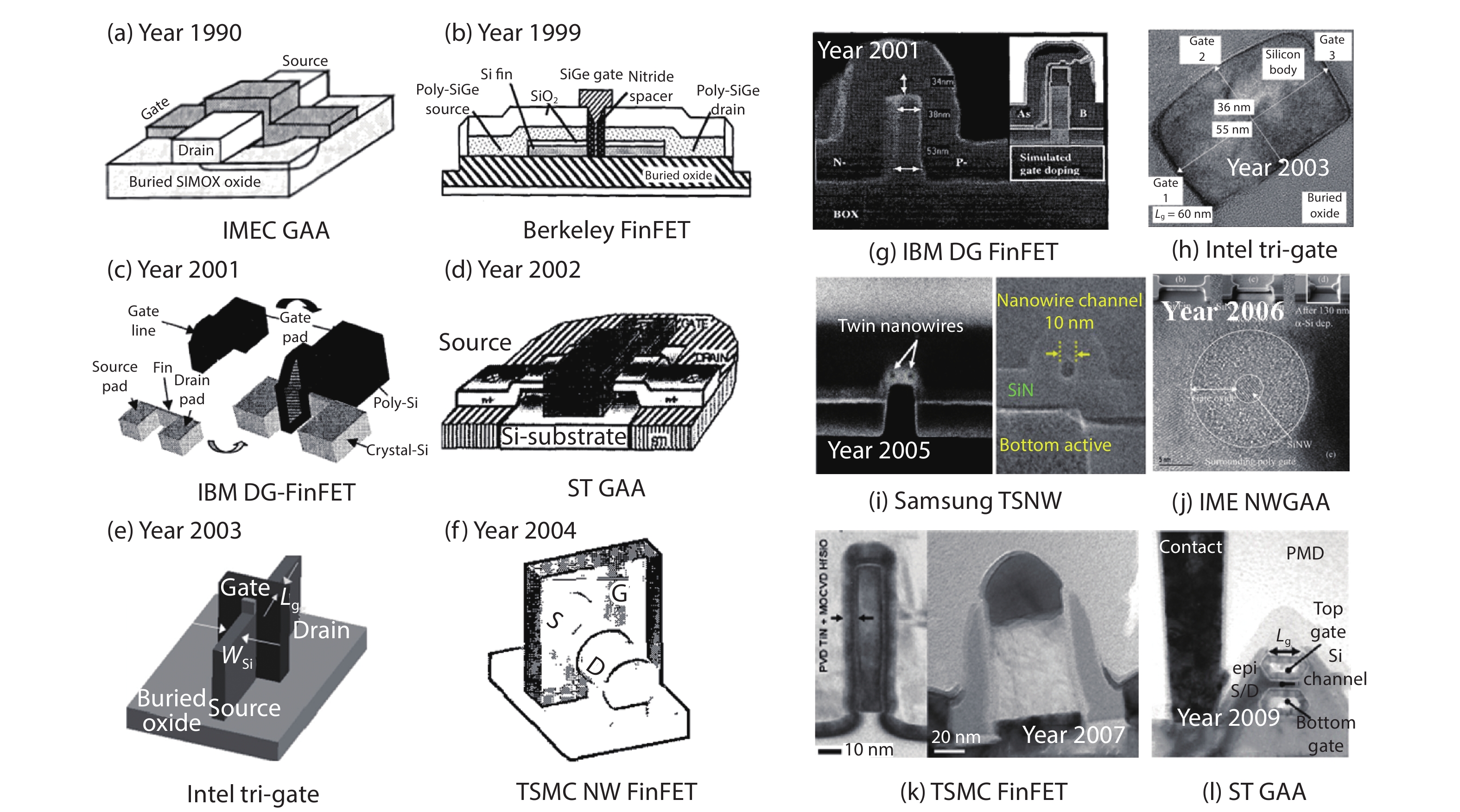
Fig. 1.  (a–f) Schematics of MuGFETs with different gate geometries: (a) IMEC’s gate-all-around (GAA) MOSFET[14], (b) the world-first FinFET[8], (c) IBM’s double-gate (DG) FinFET[11], (d) STMicroelectronics’s GAA MOSFET[15], (e) Intel’s tri-gate FinFET[10], (f) TSMC’s nanowire FinFET[16]. (g–i) TEM images showing the cross-sectional view of fins/nanowires from early works: (g) IBM’s DG FinFET[11], (h) Intel’s tri-gate FinFET[10], (i) Samsung’s nanowire MOSFET[17], (j) IME’s nanowire GAA MOSFET[18], (k) TSMC’s FinFET[27], (l) STMicroelectronics’s GAA MOSFET[28].

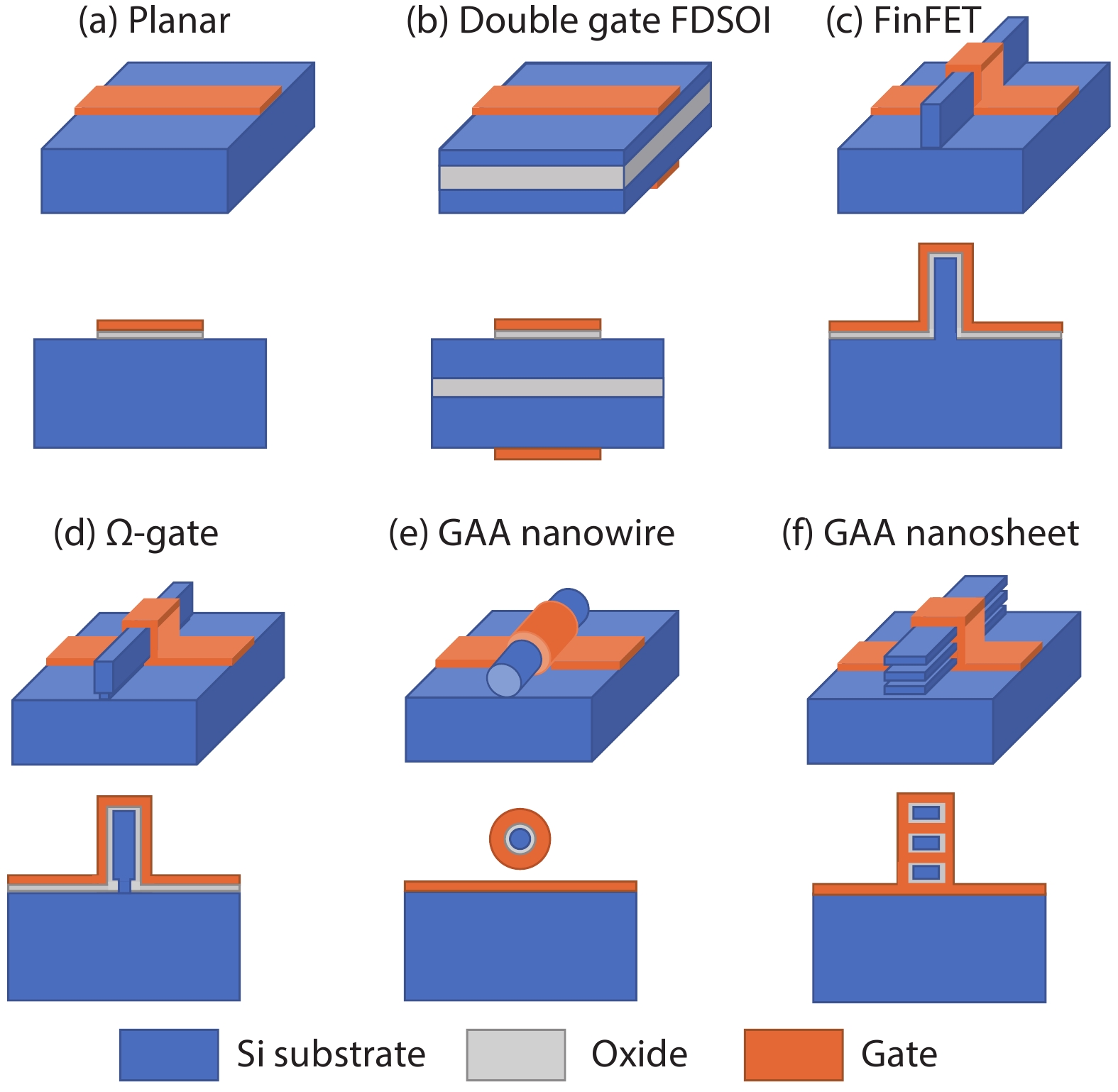
Fig. 2.  (Color online) Evolution of MuGFETs from the planar device to the stacking structures. (a) Planar MOSFET. (b) Double-gate (DG) fully depleted SOI MOSFET. (c) FinFET. (d) Ω-gate MOSFET. (e) GAA NW MOSFET. (f) GAA multilayer nanosheet MOSFET.

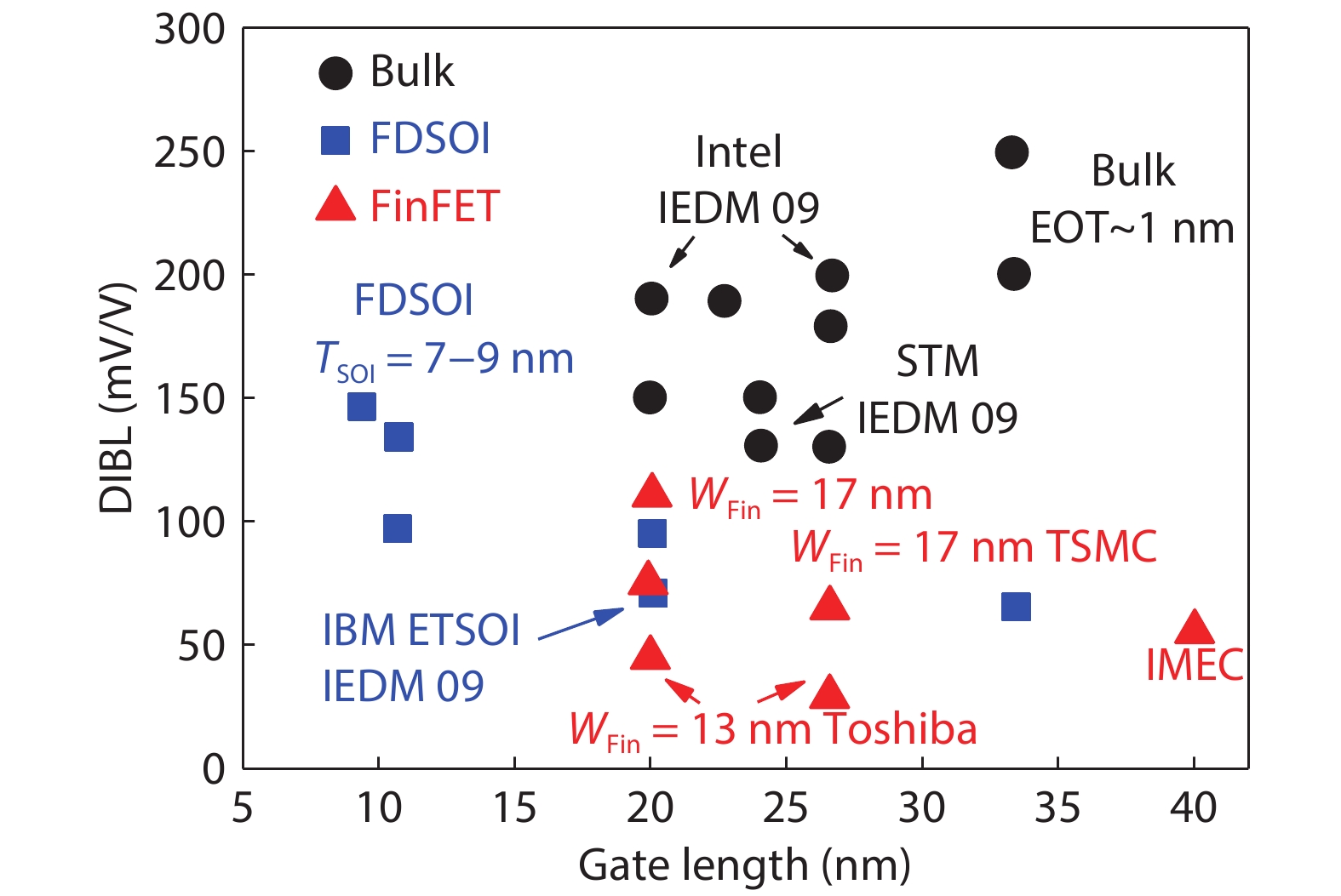
Fig. 3.  (Color online) DIBL performance as a function of gate length among FDSOI, FinFET and planar technologies[29].

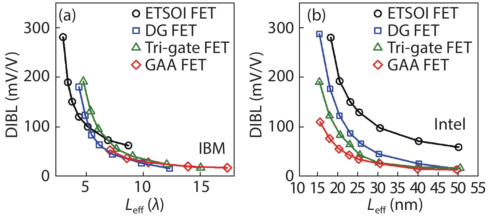
Fig. 4.  (Color online) Comparison of DIBL from ETSOI, DG, tri-gate, and GAA technologies as effective channel length reduces. Data are obtained from IBM and Intel Corp[30, 31].

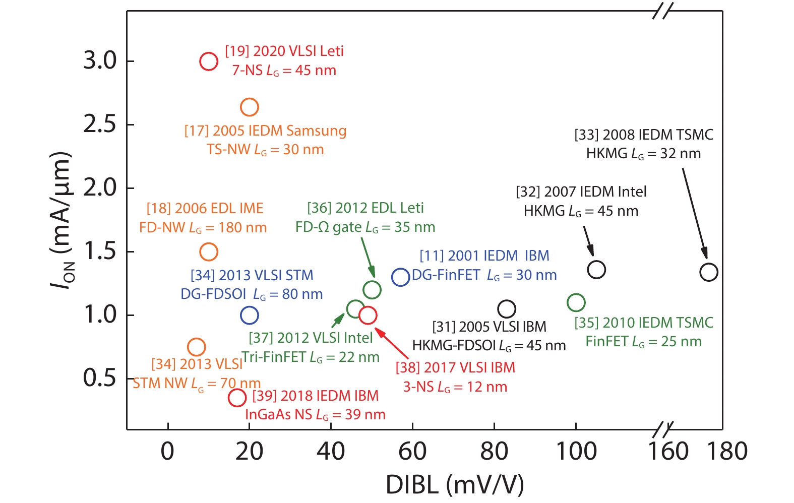
Fig. 5.  (Color online) ION–DIBL characteristics for MuGFETs with various technologies. As DIBL is a direct indicator of SCE suppression, devices with higher ION and lower DIBL suggests a better electrostatic performance[11, 1719, 3139].

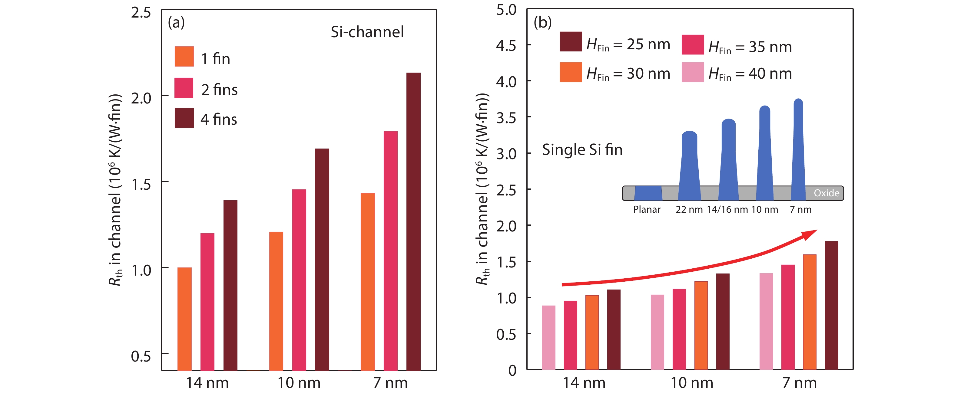
Fig. 6.  (Color online) Thermal resistivity Rth of Si fins for 14, 10 and 7 nm technology nodes as (a) the number of fins varies and (b) the fin height/aspect ratio changes[46, 47].

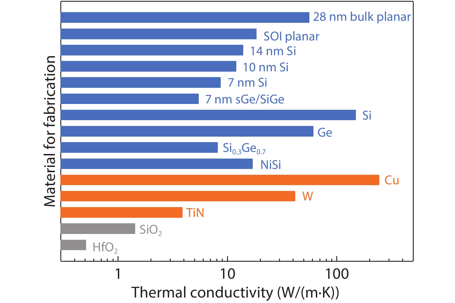
Fig. 7.  (Color online) Thermal conductivity for various materials used in gate stack, source/drain, channel, isolation and interconnects in a MuGFET. The conductivity reduces as the technology node shrinks. Higher mobility channel materials like Ge and SiGe also exhibit lower thermal conductivity[4852].

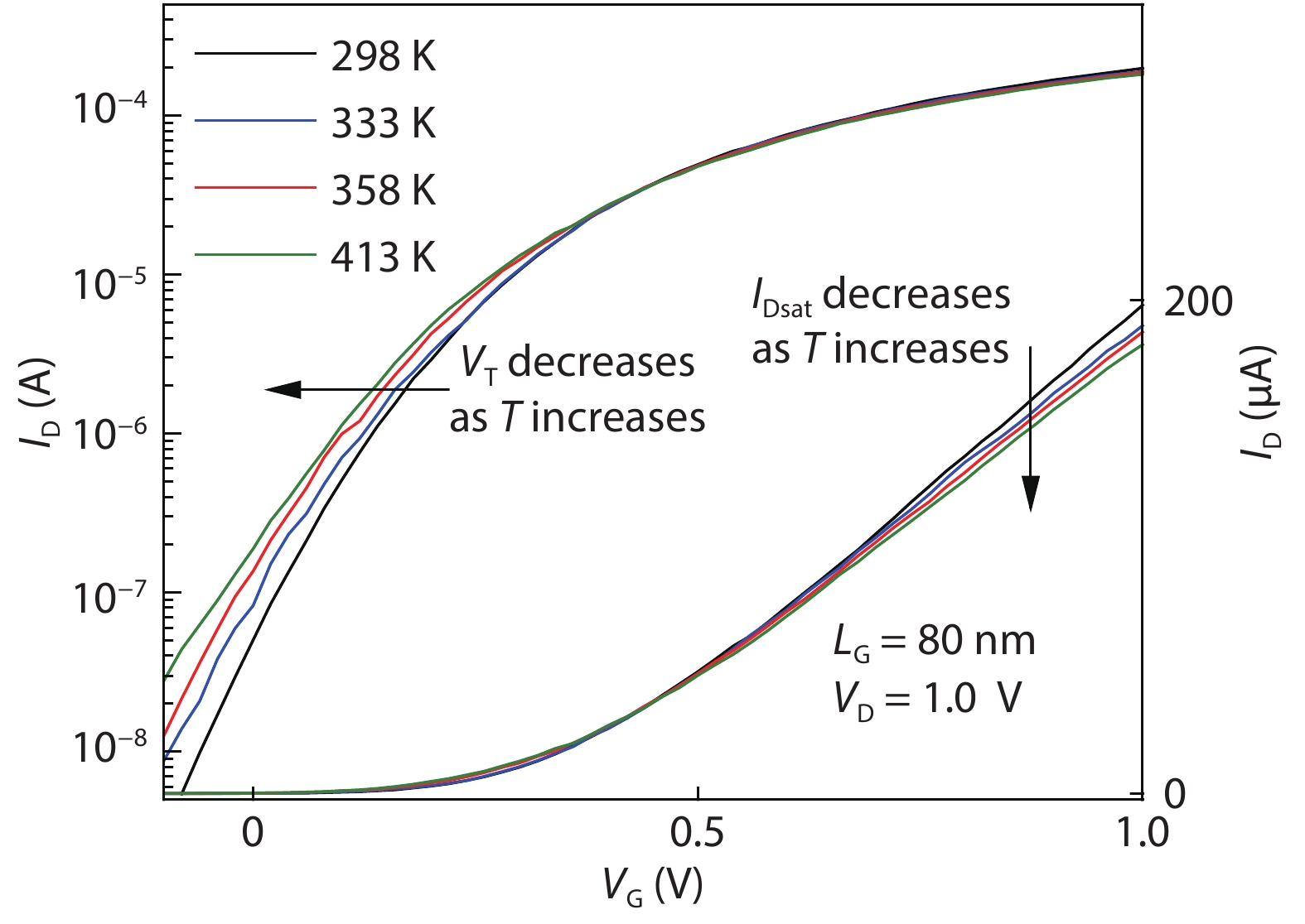
Fig. 8.  IDVG characteristics of a Si FinFET measured at drain voltage VD = 1.0 V illustrated in both logarithm (left) and linear (right) scales. The threshold voltage is taken by constant current method while IDsat is taken as the drain current at VG = VTsat + 1.0 V[24].

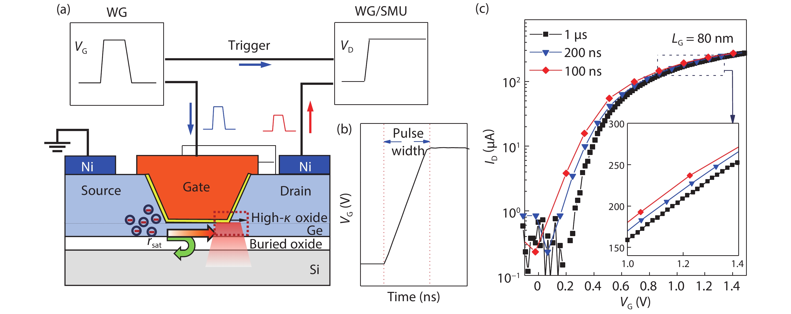
Fig. 9.  (Color online) (a) The schematic illustration of a pulsed IV testing system for a MOSFET. Pulsed signals are input at the gate electrode and sensed at the drain electrode while the source electrode is kept ground[24, 25]. (b) The waveform of VG used for the IDVG characterization. (c) IDVG characteristics of a Si FinFET (LG = 80 nm) measured at VD = 1.0 V, using pulse measurement with various pulse widths[24].

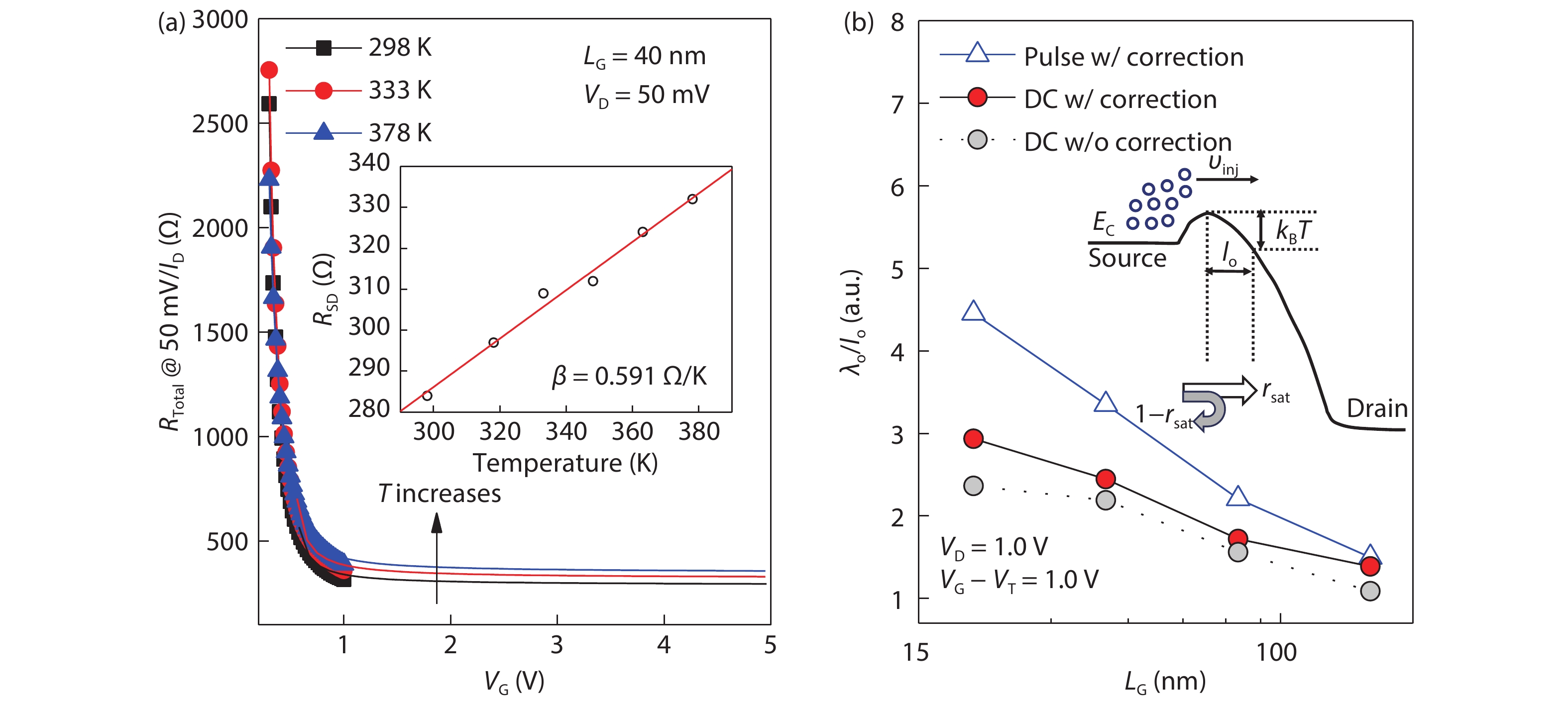
Fig. 10.  (a) Total resistance RTotal = VD/ID at VD = 50 mV as a function of VG at various characterization temperature. The experimental data (dots) fits well with the resistance model (lines)[24]. (b) Corrected λo/lo ratio for FinFETs at LG ranging from ~20 to ~150 nm, measured by both DC and pulsed I–V methods[24].

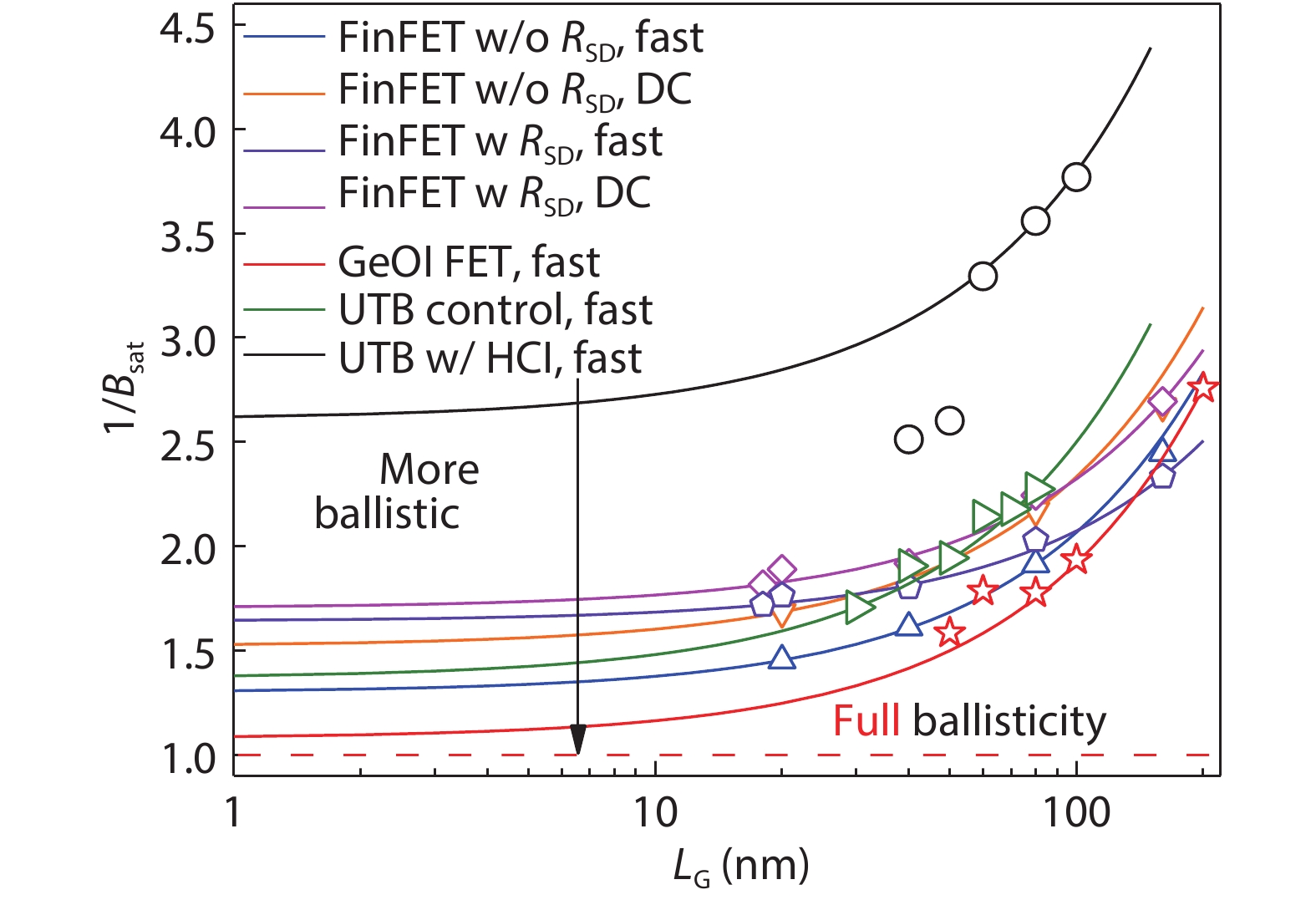
Fig. 11.  A summary of 1/Bsat as a function of LG for Si FinFETs, GeOI FETs and FDSOI/UTB FETs. Experimentally extracted Bsat before and after RSD correction, with and without SHE are provided for comparison with the simulated curves[24, 25].

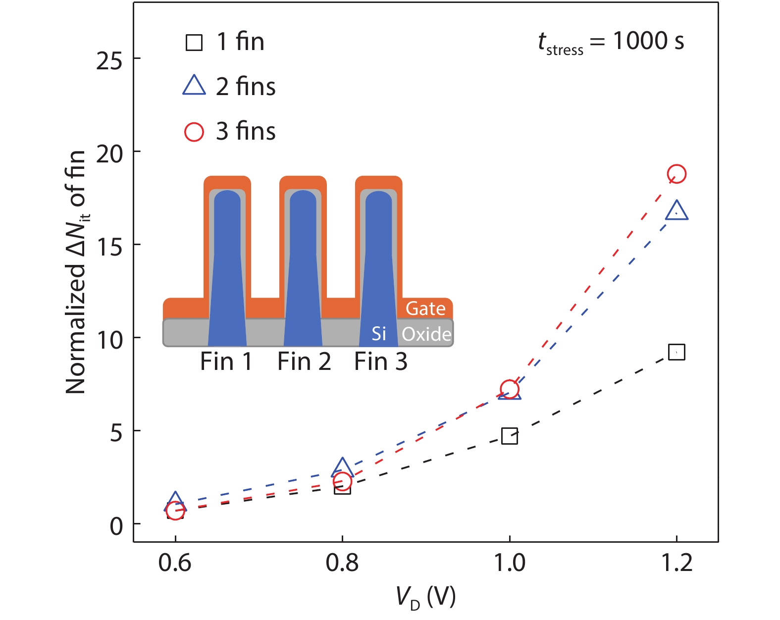
Fig. 12.  (Color online) The change of interface trap density ΔNit as the fin density and VD increase for bulk FinFETs. The stress time tstress is 1000 s[23].

Fig. 13.  (Color online) Aging contribution from NBTI, PBTI, NHCD, and PHCD are compared for 14 and 10 nm technology nodes. Since the improvement in NBTI from 14 to 10 nm node could compensate the aggravation of HCD for both p- and n-FinFETs, the end-of-line (EOL) drive for the 10 nm node actually improves by 1.65 times[45].

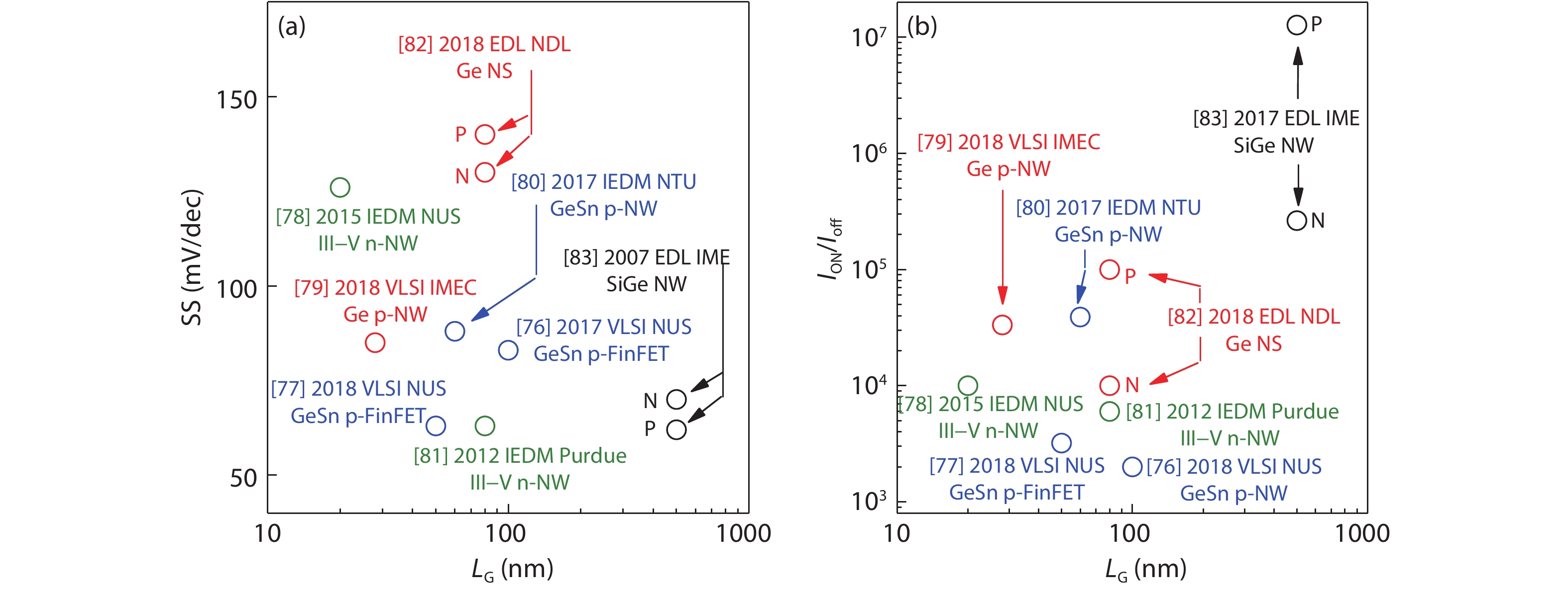
Fig. 14.  (Color online) Comparison of SS and ION/Ioff ratio at various LG for MuGFETs with novel high-mobility channels[7683].

[1]
Hofstein S R, Heiman F P. The silicon insulated-gate field-effect transistor. Proc IEEE, 1963, 51, 1190 doi: 10.1109/PROC.1963.2488
[2]
Moore G. Cramming more components onto integrated circuits. Electronics, 1965, 38, 114
[3]
Thompson S E, Armstrong M, Auth C, et al. A 90-nm logic technology featuring strained-silicon. IEEE Trans Electron Devices, 2004, 51, 1790 doi: 10.1109/TED.2004.836648
[4]
Mistry K, Allen C, Auth C, et al. A 45 nm logic technology with high-k metal gate transistors, strained silicon, 9 Cu interconnect layers, 193nm dry patterning, and 100% Pb-free packaging. IEEE International Electron Devices Meeting, 2007, 247
[5]
Auth C, Allen C, Blattner A, et al. A 22 nm high performance and low-power CMOS technology featuring fully-depleted tri-gate transistors, self-aligned contacts and high density MIM capacitors. Symp VLSI Technol VLSIT, 2012, 131
[6]
Balestra F, Cristoloveanu S, Benachir M, et al. Double-gate silicon-on-insulator transistor with volume inversion: A new device with greatly enhanced performance. IEEE Electron Device Lett, 1987, 8, 410 doi: 10.1109/EDL.1987.26677
[7]
Hisamoto D, Kaga T, Kawamoto Y, et al. A fully depleted lean-channel transistor (DELTA)-a novel vertical ultra thin SOI MOSFET. International Technical Digest on Electron Devices Meeting, 1989, 833
[8]
Huang X J, Lee W C, Kuo C, et al. Sub 50-nm FinFET: PMOS. IEEE International Electron Devices Meeting, 1999, 67
[9]
Hisamoto D, Lee W C, Kedzierski J, et al. FinFET – a self-aligned double-gate MOSFET scalable to 20 nm. IEEE Trans Electron Devices, 2000, 47, 2320 doi: 10.1109/16.887014
[10]
Doyle B S, Datta S, Doczy M, et al. High performance fully-depleted tri-gate CMOS transistors. IEEE Electron Device Lett, 2003, 24, 263 doi: 10.1109/LED.2003.810888
[11]
Kedzierski J, Fried D M, Nowak E J, et al. High-performance symmetric-gate and CMOS-compatible Vt asymmetric-gate FinFET devices. IEEE International Electron Devices Meeting, 2001, 19.5.1
[12]
Yang F L, Chen H Y, Chen F C, et al. 25 nm CMOS Omega FETs. IEEE International Electron Devices Meeting, 2002, 255
[13]
Ho B, Sun X, Xu N, et al. First demonstration of quasi-planar segmented-channel MOSFET design for improved scalability. IEEE Trans Electron Devices, 2012, 59, 2273 doi: 10.1109/TED.2012.2201721
[14]
Colinge J P, Gao M H, Romano-Rodriguez A, et al. Silicon-on-insulator ‘gate-all-around device’. International Technical Digest on Electron Devices, 1990, 595
[15]
Monfray S, Skotnicki T, Morand Y, et al. 50 nm-gate all around (GAA)-silicon on nothing (SON)-devices: A simple way to co-integration of GAA transistors within bulk MOSFET process. Symposium on VLSI Technology, 2002, 108
[16]
Yang F L, Lee D H, Chen H Y, et al. 5nm-gate nanowire FinFET. Symposium on VLSI Technology, 2004, 196
[17]
Suk S D, Lee S Y, Kim S M, et al. High performance 5nm radius twin silicon nanowire MOSFET (TSNWFET): Fabrication on bulk Si wafer, characteristics, and reliability. IEEE International Electron Devices Meeting, 2005, 181
[18]
Singh N, Agarwal A, Bera L K, et al. High-performance fully depleted silicon nanowire (diameter ≤ 5 nm) gate-all-around CMOS devices. IEEE Electron Device Lett, 2006, 27, 383 doi: 10.1109/LED.2006.873381
[19]
Barraud S, Previtali B, Vizioz C, et al. 7-levels-stacked nanosheet GAA transistors for high performance computing. IEEE Symposium on VLSI Technology, 2020, 1
[20]
Liu S E, Wang J S, Lu Y R, et al. Self-heating effect in FinFETs and its impact on devices reliability characterization. IEEE International Reliability Physics Symposium, 2014, 4A.4.1
[21]
Pop E. Energy dissipation and transport in nanoscale devices. Nano Res, 2010, 3, 147 doi: 10.1007/s12274-010-1019-z
[22]
Yin L X, Shen L, Jiang H, et al. Impact of self-heating effects on nanoscale Ge p-channel FinFETs with Si substrate. Sci China Inf Sci, 2017, 61, 1 doi: 10.1007/s11432-016-9106-x
[23]
Son D, Hong K, Shim H, et al. New insight into negative bias temperature instability degradation during self-heating in nanoscale bulk FinFETs. IEEE Electron Device Lett, 2019, 40, 1354 doi: 10.1109/LED.2019.2930077
[24]
Cheng R, Yu X, Chen B, et al. Investigation of self-heating effect on ballistic transport characterization for Si FinFETs featuring ultrafast pulsed IV technique. IEEE Trans Electron Devices, 2017, 64, 909 doi: 10.1109/TED.2016.2646907
[25]
Cheng R, Yu X, Chen B, et al. First investigation of hot carrier injection effects on ballistic transport characteristics for SOI MOSFETs featuring ultrafast pulsed IV measurement. International Reliability Physics Symposium (IRPS), 2017, 3E-3
[26]
Lim H K, Fossum J G. Threshold voltage of thin-film silicon-on-insulator (SOI) MOSFET's. IEEE Trans Electron Devices, 1983, 30, 1244 doi: 10.1109/T-ED.1983.21282
[27]
Vellianitis G, van Dal M J H, Witters L, et al. Gatestacks for scalable high-performance FinFETs. IEEE International Electron Devices Meeting, 2007, 681
[28]
Bidal G, Huguenin J L, Denorme S, et al. Gate-all-around technology: Taking advantage of ballistic transport. Proceedings of the European Solid State Device Research Conference, 2009, 315
[29]
Faynot O, Andrieu F, Weber O, et al. Planar Fully depleted SOI technology: A powerful architecture for the 20nm node and beyond. IEEE International Electron Devices Meeting, 2010, 3.2.1
[30]
Loubet N. Nanosheet transistor as a replacement of FinFET for future nodes: device advantages & specific process elements. IEEE Symposium on VLSI Technology, 2020, SC1.1
[31]
Doris B, Kim Y H, Linder B P, et al. High performance FDSOI CMOS technology with metal gate and high-k. Symposium on VLSI Technology, 2005, 214
[32]
Mistry K, Allen C, Auth C, et al. A 45 nm logic technology with high-k metal gate transistors, strained silicon, 9 Cu interconnect layers, 193nm dry patterning, and 100% Pb-free packaging. IEEE International Electron Devices Meeting, 2007, 247
[33]
Diaz C H, Goto K, Huang H T, et al. 32nm gate-first high-k/metal-gate technology for high performance low power applications. IEEE International Electron Devices Meeting, 2008, 1
[34]
Coquand R, Monfray S, Barraud S, et al. Innovative through-Si 3D lithography for ultimate self-aligned planar double-gate and gate-all-around nanowire transistors. Symposium on VLSI Technology, 2013, T226
[35]
Wu C C, Lin D W, Keshavarzi A, et al. High performance 22/20 nm FinFET CMOS devices with advanced high-k/metal gate scheme. IEEE International Electron Devices Meeting, 2010, 27.1.1
[36]
Barraud S, Coquand R, Casse M, et al. Performance of omega-shaped-gate silicon nanowire MOSFET with diameter down to 8 nm. IEEE Electron Device Lett, 2012, 33, 1526 doi: 10.1109/LED.2012.2212691
[37]
Auth C, Allen C, Blattner A, et al. A 22 nm high performance and low-power CMOS technology featuring fully-depleted tri-gate transistors, self-aligned contacts and high density MIM capacitors. Symposium on VLSI Technology (VLSIT), 2012, 131
[38]
Loubet N, Hook T, Montanini P, et al. Stacked nanosheet gate-all-around transistor to enable scaling beyond FinFET. Symposium on VLSI Technology, 2017, T230
[39]
Lee S, Cheng C W, Sun X, et al. High performance InGaAs gate-all-around nanosheet FET on Si using template assisted selective epitaxy. IEEE International Electron Devices Meeting (IEDM), 2018, 39.5.1
[40]
Chaudhary A, Kaczer B, Roussel P J, et al. Time dependent variability in RMG-HKMG FinFETs: Impact of extraction scheme on stochastic NBTI. IEEE International Reliability Physics Symposium, 2015, 3B.4.1
[41]
Xu M, Yin H X, Zhu H L, et al. Device parameter optimization for sub-20 nm node HK/MG-last bulk FinFETs. J Semicond, 2015, 36, 044007 doi: 10.1088/1674-4926/36/4/044007
[42]
Deleonibus S. Ultra-thin films and multigate devices architectures for future CMOS scaling. Sci China Inf Sci, 2011, 54, 990 doi: 10.1007/s11432-011-4231-x
[43]
Jurczak M, Collaert N, Veloso A, et al. Review of FINFET technology. IEEE International SOI Conference, 2009, 1
[44]
Malinowski A, Chen J, Mishra S K, et al. What is killing Moore's Law, challenges in advanced FinFET technology integration. MIXDES - 26th International Conference Mixed Design of Integrated Circuits and Systems, 2019, 46
[45]
Rahman A, Dacuna J, Nayak P, et al. Reliability studies of a 10nm high-performance and low-power CMOS technology featuring 3rd generation FinFET and 5th generation HK/MG. IEEE International Reliability Physics Symposium (IRPS), 2018, 6F.4
[46]
Moroz V. Technology inflection points: Planar to FinFET to nanowire. Int Symp Phys Design, 2016
[47]
Jang D, Bury E, Ritzenthaler R, et al. Self-heating on bulk FinFET from 14nm down to 7nm node. IEEE International Electron Devices Meeting (IEDM), 2015, 11.6.1
[48]
Aksamija Z, Knezevic I. Thermal conductivity of Si1– xGex/Si1– yGe y superlattices: Competition between interfacial and internal scattering. Phys Rev B, 2013, 88, 155318 doi: 10.1103/PhysRevB.88.155318
[49]
Bury E, Kaczer B, Mitard J, et al. Characterization of self-heating in high-mobility Ge FinFET pMOS devices. IEEE Symp VLSI Technol VLSI Technol, 2015, T60
[50]
Pop E, Sinha S, Goodson K E. Heat generation and transport in nanometer-scale transistors. Proc IEEE, 2006, 94, 1587 doi: 10.1109/JPROC.2006.879794
[51]
Terada Y, Ohkubo K, Mohri T, et al. Thermal conductivity of cobalt-base alloys. Metall Mater Trans A, 2003, 34, 2026 doi: 10.1007/s11661-003-0168-z
[52]
Zhao Y, Qu Y M. Impact of self-heating effect on transistor characterization and reliability issues in sub-10 nm technology nodes. IEEE J Electron Devices Soc, 2019, 7, 829 doi: 10.1109/JEDS.2019.2911085
[53]
Chen W C, Cheng R, Wang D W, et al. Electrothermal effects on hot-carrier reliability in SOI MOSFETs—AC versus circuit-speed random stress. IEEE Trans Electron Devices, 2016, 63, 3669 doi: 10.1109/TED.2016.2591767
[54]
Wang R S, Zhuge J, Liu C Z, et al. Experimental study on quasi-ballistic transport in silicon nanowire transistors and the impact of self-heating effects. IEEE International Electron Devices Meeting, 2008, 1
[55]
Jiang H, Liu X Y, Xu N, et al. Investigation of self-heating effect on hot carrier degradation in multiple-fin SOI FinFETs. IEEE Electron Device Lett, 2015, 36, 1258 doi: 10.1109/LED.2015.2487045
[56]
Yamane T, Nagai N, Katayama S I, et al. Measurement of thermal conductivity of silicon dioxide thin films using a 3ω method. J Appl Phys, 2002, 91, 9772 doi: 10.1063/1.1481958
[57]
Lundstrom M. Elementary scattering theory of the Si MOSFET. IEEE Electron Device Lett, 1997, 18, 361 doi: 10.1109/55.596937
[58]
Lundstrom M S. On the mobility versus drain current relation for a nanoscale MOSFET. IEEE Electron Device Lett, 2001, 22, 293 doi: 10.1109/55.924846
[59]
Chen M J, Huang H T, Huang K C, et al. Temperature dependent channel backscattering coefficients in nanoscale MOSFETs. IEEE International Electron Devices Meeting, 2002, 39
[60]
Liow T Y, Tan K M, Chin H C, et al. Carrier transport characteristics of sub-30 nm strained N-channel FinFETs featuring silicon-carbon source/drain regions and methods for further performance enhancement. IEEE International Electron Devices Meeting, 2006, 1
[61]
Dixit A, Kottantharayil A, Collaert N, et al. Analysis of the parasitic S/D resistance in multiple-gate FETs. IEEE Trans Electron Devices, 2005, 52, 1132 doi: 10.1109/TED.2005.848098
[62]
Tomita R, Kimura H, Yasuda M, et al. Improvement on sheet resistance uniformity of nickel silicide by optimization of silicidation conditions. Microelectron Reliab, 2013, 53, 665 doi: 10.1016/j.microrel.2012.12.011
[63]
Matsukawa T, Liu Y X, Endo K, et al. Variability origins of parasitic resistance in FinFETs with silicided source/drain. IEEE Electron Device Lett, 2012, 33, 474 doi: 10.1109/LED.2012.2182755
[64]
Su P H, Li Y M. Determination of source-and-drain series resistance in 16-nm-gate FinFET devices. IEEE Trans Electron Devices, 2015, 62, 1663 doi: 10.1109/TED.2015.2418091
[65]
Choudhury N, Sharma U, Zhou H M, et al. Analysis of BTI, SHE induced BTI and HCD under full VG/VD space in GAA nano-sheet N and P FETs. IEEE International Reliability Physics Symposium (IRPS), 2020, 1
[66]
Prasad C. A review of self-heating effects in advanced CMOS technologies. IEEE Trans Electron Devices, 2019, 66, 4546 doi: 10.1109/TED.2019.2943744
[67]
Wang M M, Zhang J Y, Zhou H M, et al. Bias temperature instability reliability in stacked gate-all-around nanosheet transistor. IEEE International Reliability Physics Symposium (IRPS), 2019, 1
[68]
Pande N, Zhou C, Lin M, et al. Characterizing electromigration effects in a 16nm FinFET process using a circuit based test vehicle. IEEE International Electron Devices Meeting (IEDM), 2019, 5.3.1
[69]
Zhang R, Yang K X, Liu T Z, et al. New electromigration model and its potential application on degradation simulation for FinFET SRAM. International Integrated Reliability Workshop (IIRW), 2018, 1
[70]
Liu C Z, Zou J B, Wang R S, et al. Towards the systematic study of aging induced dynamic variability in nano-MOSFETs: Adding the missing cycle-to-cycle variation effects into device-to-device variation. IEEE International Electron Devices Meeting, 2011, 25.4.1
[71]
Wu W K, An X, Jiang X B, et al. Line-edge roughness induced single event transient variation in SOI FinFETs. J Semicond, 2015, 36, 114001 doi: 10.1088/1674-4926/36/11/114001
[72]
Chen J Z, Nakasaki Y, Mitani Y. Deep insight into process-induced pre-existing traps and PBTI stress-induced trap generations in high-k gate dielectrics through systematic RTN characterizations and ab initio calculations. IEEE Symposium on VLSI Technology, 2016, 1
[73]
Zhan X P, Xi Y F, Wang Q W, et al. Dual-point technique for multi-trap RTN signal extraction. IEEE Access, 2020, 8, 88141 doi: 10.1109/ACCESS.2020.2993612
[74]
Mei S, Raghavan N, Bosman M, et al. New understanding of dielectric breakdown in advanced FinFET devices—physical, electrical, statistical and multiphysics study. IEEE International Electron Devices Meeting (IEDM), 2016, 15.5.1
[75]
Feijoo P C, Kauerauf T, Toledano-Luque M, et al. Time-dependent dielectric breakdown on subnanometer EOT nMOS FinFETs. IEEE Trans Device Mater Reliab, 2012, 12, 166 doi: 10.1109/TDMR.2011.2180387
[76]
Lei D, Lee K H, Bao S Y, et al. The first GeSn FinFET on a novel GeSnOI substrate achieving lowest S of 79 mV/decade and record high Gm, int of 807 μS/μm for GeSn P-FETs. Symposium on VLSI Technology, 2017, T198
[77]
Lei D, Han K Z, Lee K H, et al. GeSn p-FinFETs with sub-10 nm Fin width realized on a 200 mm GeSnOI Substrate: Lowest SS of 63 mV/decade, highest Gm, int of 900 μS/μm, and high-field μeff of 275 cm2/(V·s). IEEE Symposium on VLSI Technology, 2018, 197
[78]
Goh K H, Tan K H, Yadav S, et al. Gate-all-around CMOS (InAs n-FET and GaSb p-FET) based on vertically-stacked nanowires on a Si platform, enabled by extremely-thin buffer layer technology and common gate stack and contact modules. IEEE International Electron Devices Meeting (IEDM), 2015, 15.4.1
[79]
Mitard J, Jang D, Eneman G, et al. An in-depth study of high-performing strained germanium nanowires pFETs. IEEE Symposium on VLSI Technology, 2018, 83
[80]
Huang Y S, Lu F L, Tsou Y J, et al. First vertically stacked GeSn nanowire pGAAFETs with Ion = 1850 μA/μm (Vov = Vds = −1 V) on Si by GeSn/Ge CVD epitaxial growth and optimum selective etching. IEEE International Electron Devices Meeting (IEDM), 2017, 37.5.1
[81]
Gu J J, Wang X W, Wu H, et al. 20–80 nm Channel length InGaAs gate-all-around nanowire MOSFETs with EOT = 1.2 nm and lowest SS = 63 mV/dec. IEEE International Electron Devices Meeting, 2012, 27.6.1
[82]
Chu C L, Wu K, Luo G L, et al. Stacked Ge-nanosheet GAAFETs fabricated by Ge/Si multilayer epitaxy. IEEE Electron Device Lett, 2018, 39, 1133 doi: 10.1109/LED.2018.2850366
[83]
Fang W W, Singh N, Bera L K, et al. Vertically stacked SiGe nanowire array channel CMOS transistors. IEEE Electron Device Lett, 2007, 28, 211 doi: 10.1109/LED.2007.891268
[84]
Gong X, Han G Q, Bai F, et al. Germanium–tin (GeSn) p-channel MOSFETs fabricated on (100) and (111) surface orientations with sub-400 °C Si2H6 passivation. IEEE Electron Device Lett, 2013, 34, 339 doi: 10.1109/LED.2012.2236880
[85]
Gong X, Zhou Q, Owen M H S, et al. InAlP-Capped (100) Ge nFETs with 1.06 nm EOT: Achieving record high peak mobility and first integration on 300 mm Si substrate. IEEE International Electron Devices Meeting, 2014, 9.4.1
[86]
Liu B, Gong X, Han G Q, et al. High-performance germanium ω-gate MuGFET with Schottky-barrier nickel germanide source/drain and low-temperature disilane-passivated gate stack. IEEE Electron Device Lett, 2012, 33, 1336 doi: 10.1109/LED.2012.2207368
[87]
Lee C H, Nishimura T, Tabata T, et al. Ge MOSFETs performance: Impact of Ge interface passivation. IEEE International Electron Devices Meeting, 2010, 18.1.1
[88]
Zhang R, Iwasaki T, Taoka N, et al. Al2O3/GeOx/Ge gate stacks with low interface trap density fabricated by electron cyclotron resonance plasma postoxidation. Appl Phys Lett, 2011, 98, 112902 doi: 10.1063/1.3564902
[89]
Mitard J, Shea C, DeJaeger B, et al. Impact of EOT scaling down to 0.85 nm on 70 nm Ge-pFETs technology with STI. VLSI Symp Tech Dig, 2009, 82
[90]
Franco J, Kaczer B, Mitard J, et al. NBTI reliability of SiGe and Ge channel pMOSFETs with SiO2/HfO2 dielectric stack. IEEE Trans Device Mater Reliab, 2013, 13, 497 doi: 10.1109/TDMR.2013.2281731
  • Search

    Advanced Search >>

    GET CITATION

    shu

    Export: BibTex EndNote

    Article Metrics

    Article views: 5665 Times PDF downloads: 459 Times Cited by: 0 Times

    History

    Received: 19 January 2021 Revised: 31 January 2021 Online: Accepted Manuscript: 01 February 2021Uncorrected proof: 03 February 2021Published: 08 February 2021

    Catalog

      Email This Article

      User name:
      Email:*请输入正确邮箱
      Code:*验证码错误
      Ying Sun, Xiao Yu, Rui Zhang, Bing Chen, Ran Cheng. The past and future of multi-gate field-effect transistors: Process challenges and reliability issues[J]. Journal of Semiconductors, 2021, 42(2): 023102. doi: 10.1088/1674-4926/42/2/023102 Y Sun, X Yu, R Zhang, B Chen, R Cheng, The past and future of multi-gate field-effect transistors: Process challenges and reliability issues[J]. J. Semicond., 2021, 42(2): 023102. doi: 10.1088/1674-4926/42/2/023102.Export: BibTex EndNote
      Citation:
      Ying Sun, Xiao Yu, Rui Zhang, Bing Chen, Ran Cheng. The past and future of multi-gate field-effect transistors: Process challenges and reliability issues[J]. Journal of Semiconductors, 2021, 42(2): 023102. doi: 10.1088/1674-4926/42/2/023102

      Y Sun, X Yu, R Zhang, B Chen, R Cheng, The past and future of multi-gate field-effect transistors: Process challenges and reliability issues[J]. J. Semicond., 2021, 42(2): 023102. doi: 10.1088/1674-4926/42/2/023102.
      Export: BibTex EndNote

      The past and future of multi-gate field-effect transistors: Process challenges and reliability issues

      doi: 10.1088/1674-4926/42/2/023102
      More Information
      • Author Bio:

        Ying Sun received the B.S degree in Hefei University of Technology in 2018. She is currently a Ph.D candidate with the College of Micro-Nano Electronics, Zhejiang University. Her research focuses on the device characterization and reliability analysis for advanced CMOS transistors

        Ran Cheng received the B.Eng. and Ph.D degrees in Electrical Engineering from National University of Singapore, Singapore in 2009 and 2014, respectively. From late 2014, she joined Zhejiang University. Her research interests include strain engineering, device modelling, fast and cyrogenic characterization for advanced transistors. She has authored and co-authored over 50 publications. She is currently an Associate Professor with School of Micro-Nano Electronics, Zhejiang University, China

      • Corresponding author: chengran@zju.edu.cn
      • Received Date: 2021-01-19
      • Revised Date: 2021-01-31
      • Published Date: 2021-02-10

      Catalog

        /

        DownLoad:  Full-Size Img  PowerPoint
        Return
        Return