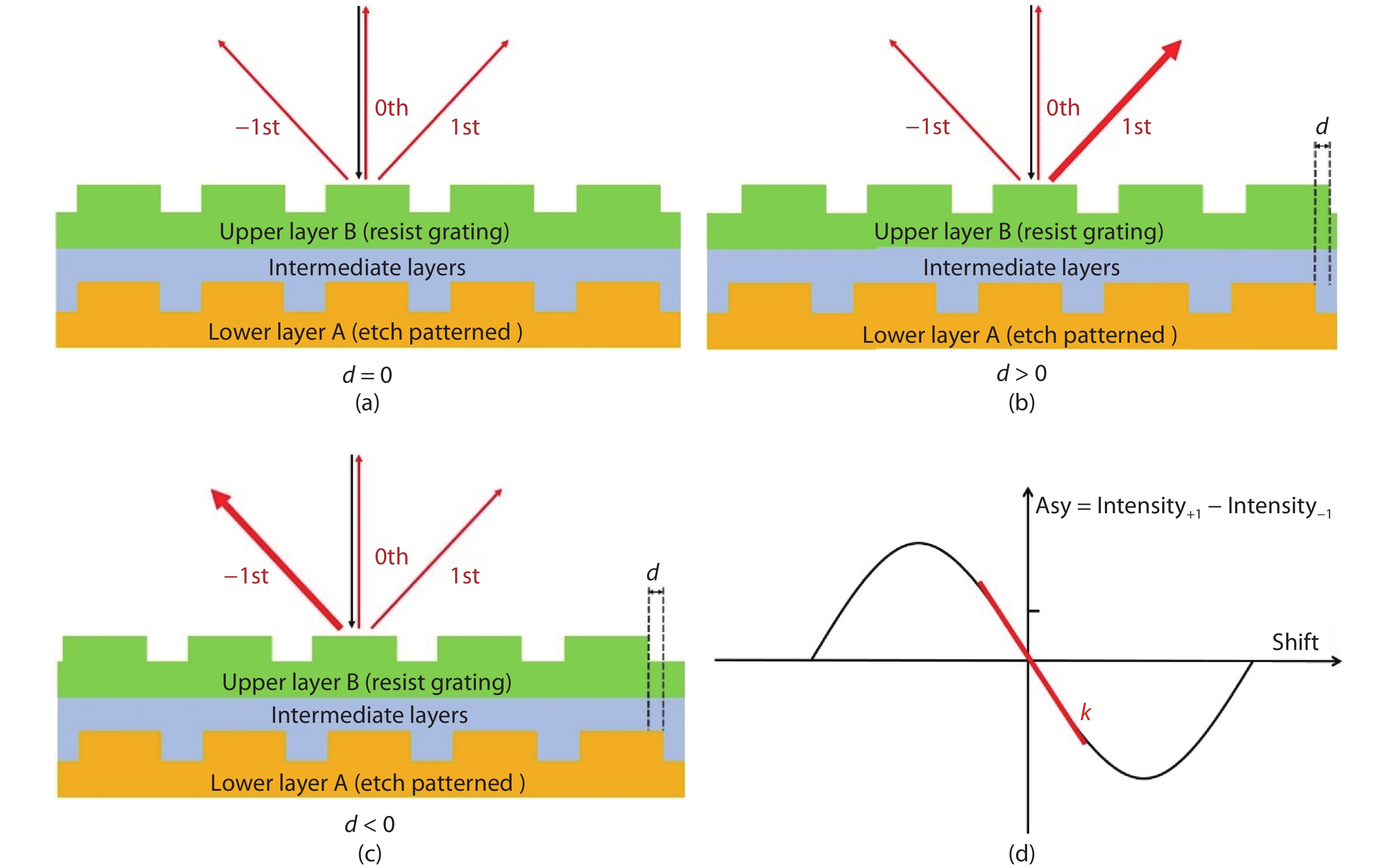
Fig. 1.
(Color online) Schematic of the difference of + 1 and –1 diffraction order intensities when (a) d = 0, (b) d > 0, (c) d < 0. (d) Liner relationship between the difference of intensity and d.
ARTICLES
Buqing Xu1, 3, Qiang Wu2, Lisong Dong3 and Yayi Wei1, 3,
Corresponding author: Yayi Wei, E-mail: weiyayi@ime.ac.cn
Abstract: A physical model for simulating overlay metrology employing diffraction based overlay (DBO) principles is built. It can help to optimize the metrology wavelength selection in DBO. Simulation result of DBO metrology with a model based on the finite-difference time-domain (FDTD) method is presented. A common case (bottom mark asymmetry) in which error signals are always induced in DBO measurement due to the process imperfection were discussed. The overlay sensitivity of the DBO measurement across the visible illumination spectrum has been performed and compared. After adjusting the model parameters compatible with the actual measurement conditions, the metrology wavelengths which provide the accuracy and robustness of DBO measurement can be optimized.
Key words: diffraction based overlay, scatterometry, photolithography simulation, metrology wavelength, finite difference time domain
| [1] |
Simon C, Hsu C, Pai Y C, et al. Scatterometry or imaging overlay: a comparative study. Proc SPIE, 2015, 9424, 942409 doi: 10.1117/12.2085950
|
| [2] |
Kim T S, Park Y S, Kim Y C, et al. Improved control of multi-layer overlay in advanced 8 nm logic nodes. Proc SPIE, 2018, 10585, 1058529 doi: 10.1117/12.2297099
|
| [3] |
Bishoff J, Brunner R, Bauer J, et al. Light diffraction based overlay measurement. Proc SPIE, 2001, 4344, 222 doi: 10.1117/12.436745
|
| [4] |
Dinu B, Fuchs S, Kramer U, et al. Overlay control using scatterometry based metrology (SCOM) in production environment. Proc SPIE, 2008, 6922, 6922S doi: 10.1117/12.771581
|
| [5] |
Leray P, Laidler D, Cheng S, et al. Achieving optimum diffraction based overlay performance. Proc SPIE, 2010, 7638, 76382B doi: 10.1117/12.848524
|
| [6] |
Leray P, Laidler D, D'Havé K, et al. Diffraction based overlay re-assessed. Proc SPIE, 2011, 7971, 797114 doi: 10.1117/12.882353
|
| [7] |
Yang W, Lowe-Webb R, J. Heaton J, et al Alignment and overlay metrology using a spectroscopic diffraction method. Advanced Semiconductor Manufacturing Conference and Workshop, 2003, 45 doi: 10.1109/ASMC.2003.1194465
|
| [8] |
Zhu L, Li J, Zhou C S, et al. Overlay mark optimization for thick-film resist overlay metrology. J Semicond, 2009, 30(6), 066002 doi: 10.1088/1674-4926/30/6/066002
|
| [9] |
Dasari P, Smith N, Goelzer G, et al. A comparison of advanced overlay technologies. Proc SPIE, 2010, 7638, 76381P doi: 10.1117/12.848189
|
| [10] |
Li J, Liu Z, S. Rabello S, et al Simultaneous overlay and CD measurement for double patterning: scatterometry and RCWA approach. Proc SPIE, 2009, 7272, 727207 doi: 10.1117/12.814706
|
| [11] |
Ke C M, Huang G T, Huang J. Accuracy of diffraction-based and image-based overlay. Proc SPIE, 2011, 7971, 79711E doi: 10.1117/12.880037
|
| [12] |
Bhattacharyya K, Boef A D, Noot M, et al. A complete methodology towards accuracy and lot-to-lot robustness in on-product overlay metrology using flexible wavelength selection. Proc SPIE, 2017, 10145, 101450A doi: 10.1117/12.2257662
|
| [13] |
Oh S H, Lee J, Lee S, et al. The effect of individually-induced processes on image-based overlay and diffraction-based overlay. Proc SPIE, 2014, 9050, 905039 doi: 10.1117/12.2046583
|
| [14] |
Zhou Y, Park D, Gutjahr K, et al. Reducing the overlay metrology sensitivity to perturbations of the measurement stack. Proc SPIE, 2017, 10145, 101452G doi: 10.1117/12.2257913
|
| [15] |
Bhattacharyya K, Ke C M, Huang G T, et al. On-product overlay enhancement using advanced litho-cluster control based on integrated metrology, ultra-small DBO targets and novel corrections. Proc SPIE, 2013, 8681, 868104 doi: 10.1117/12.2011878
|
| [16] |
Bhattacharyya K, Boef A D, G. Storms G, et al A study of swing-curve physics in diffraction-based overlay. Proc SPIE, 2016, 9778, 97781l doi: 10.1117/12.2222040
|
| [17] |
Boef A D, Bhattacharyya K, Noot M, et al. Monitoring accuracy and robustness in on-product diffraction-based overlay metrology. International Conference on Frontiers of Characterization and Metrology for Nanoelectronics, 2017, 191
|
| [18] |
Wei Y. Theory and application of advanced lithography for VLSI. Beijing: Science Press, 2016, 296
|
| [19] |
Yee K S. Numerical solution of initial boundary value problems involving Maxwell’s equations in isotropic media. IEEE Trans Anten Propag, 1966, 14(3), 302 doi: 10.1109/TAP.1966.1138693
|
| [20] |
Elsherbeni A Z, Demir V. The finite-difference time-domain for electromagnetics with MATLAB simulations. SciTech Publishing, 2006, 5
|
| [21] |
Ge D B, Yan Y B. Finite-difference time-domain method for electromagnetic waves. Xi’an: Xidian University Press, 2011, 10
|
| [22] |
Liu R R, Wang Y B, Yin D D, et al. A high-efficiency grating coupler between single-mode fiber and silicon-on-insulator waveguide. J Semicond, 2017, 38(5), 054007 doi: 10.1088/1674-4926/38/5/054007
|
| [23] |
Mur G. Absorbing boundary conditions for finite difference approximation of the time domain electromagnetic field equations. IEEE Trans Electromagn Compat, 1981, 23(4), 377 doi: 10.1109/TEMC.1981.303970
|
| [24] |
Schaepkens M, Oehrlein G S. Asymmetric microtrenching during inductively coupled plasma oxide etching in the presence of a weak magnetic field. Appl Phys Lett, 1998, 72, 1293 doi: 10.1063/1.121068
|
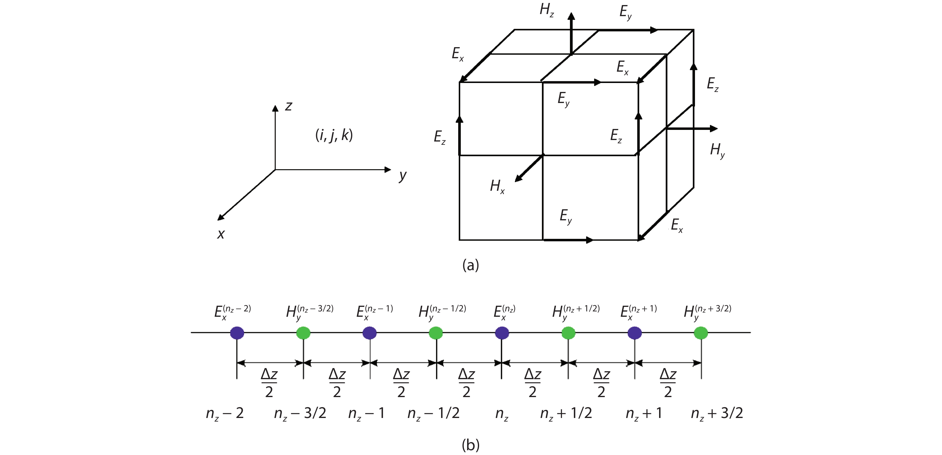
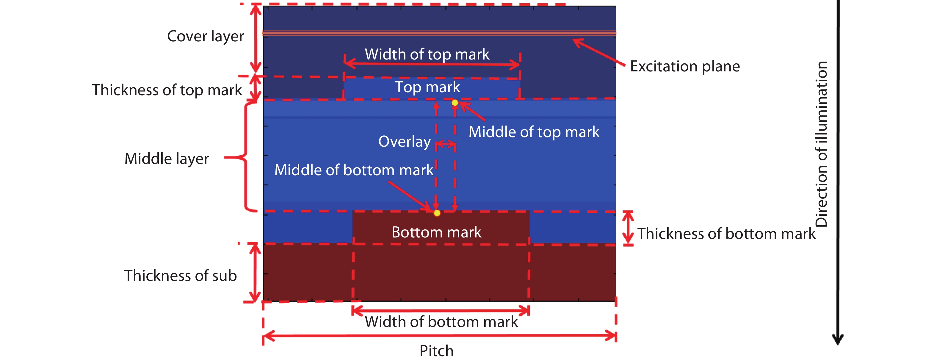
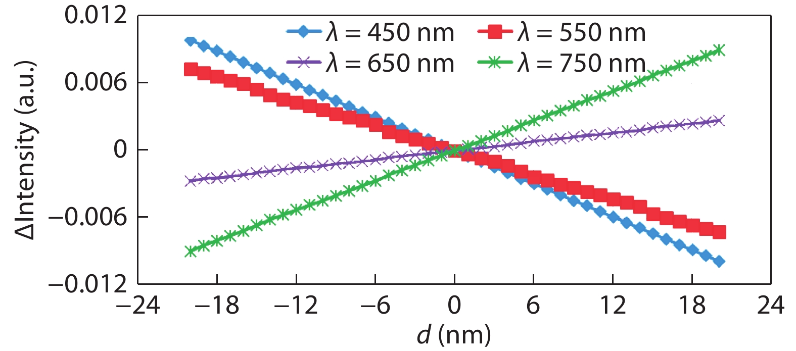
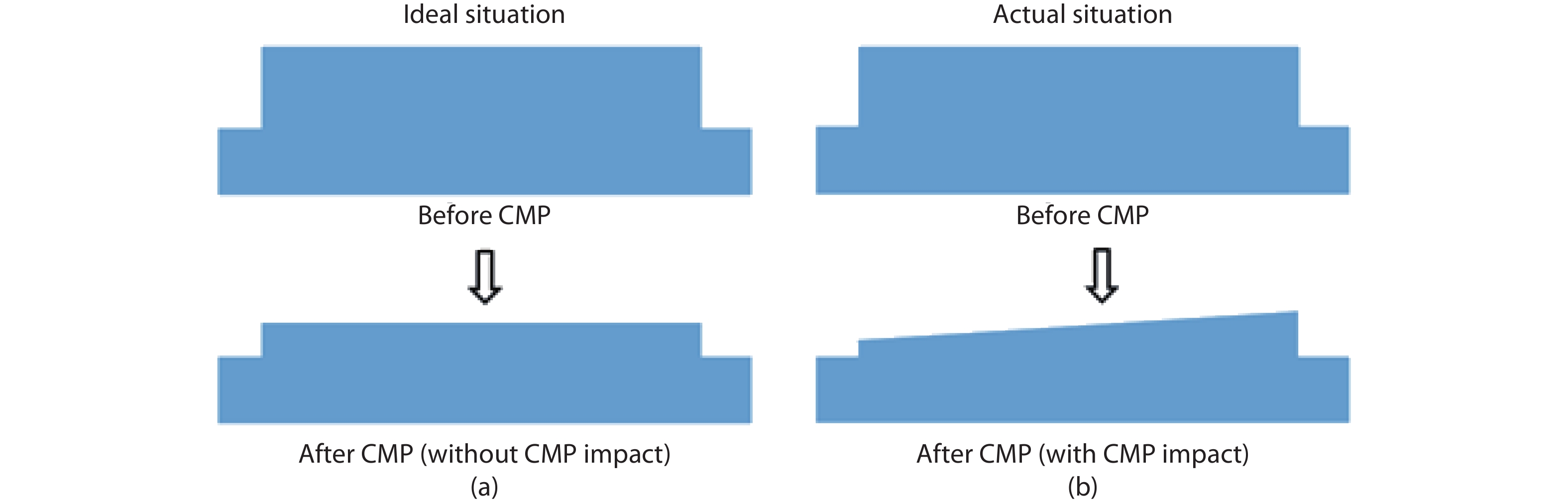
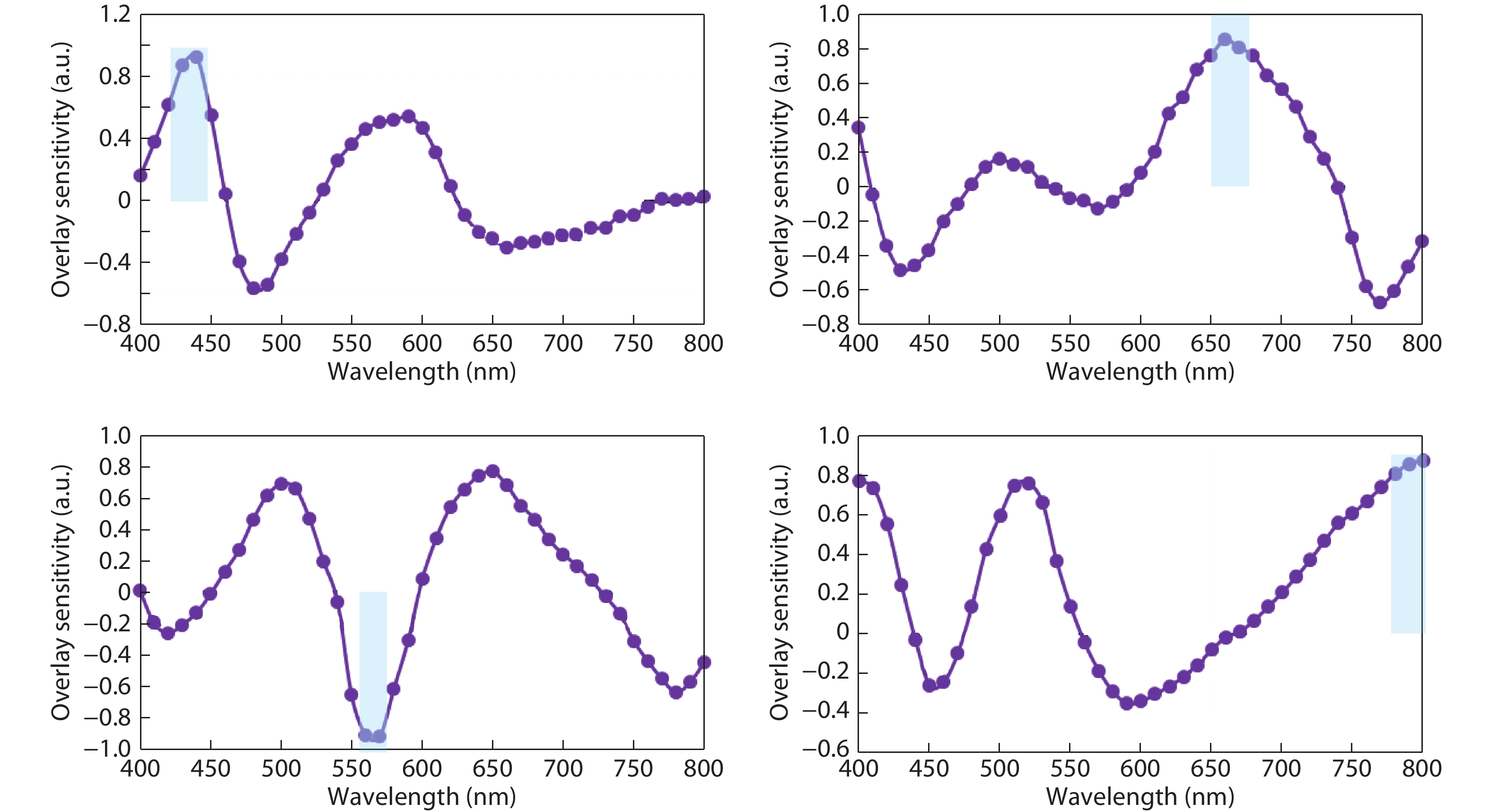
Table 1. Space coordinates and time steps of E and H components in Yee cell.
| Electromagnetic field component | Sampling of space components | Sampling of the time axis (t) | |||
| x coordinate | y coordinate | z coordinate | |||
| E node | Ex | i + 1/2 | j | k | n |
| Ey | i | j + 1/2 | k | n | |
| Ez | i | j | k + 1/2 | n | |
| H node | Hx | i | j + 1/2 | k + 1/2 | n + 1/2 |
| Hy | i + 1/2 | j | k + 1/2 | n + 1/2 | |
| Hz | i + 1/2 | j + 1/2 | k | n + 1/2 | |
 DownLoad: CSV
| [1] |
Simon C, Hsu C, Pai Y C, et al. Scatterometry or imaging overlay: a comparative study. Proc SPIE, 2015, 9424, 942409 doi: 10.1117/12.2085950
|
| [2] |
Kim T S, Park Y S, Kim Y C, et al. Improved control of multi-layer overlay in advanced 8 nm logic nodes. Proc SPIE, 2018, 10585, 1058529 doi: 10.1117/12.2297099
|
| [3] |
Bishoff J, Brunner R, Bauer J, et al. Light diffraction based overlay measurement. Proc SPIE, 2001, 4344, 222 doi: 10.1117/12.436745
|
| [4] |
Dinu B, Fuchs S, Kramer U, et al. Overlay control using scatterometry based metrology (SCOM) in production environment. Proc SPIE, 2008, 6922, 6922S doi: 10.1117/12.771581
|
| [5] |
Leray P, Laidler D, Cheng S, et al. Achieving optimum diffraction based overlay performance. Proc SPIE, 2010, 7638, 76382B doi: 10.1117/12.848524
|
| [6] |
Leray P, Laidler D, D'Havé K, et al. Diffraction based overlay re-assessed. Proc SPIE, 2011, 7971, 797114 doi: 10.1117/12.882353
|
| [7] |
Yang W, Lowe-Webb R, J. Heaton J, et al Alignment and overlay metrology using a spectroscopic diffraction method. Advanced Semiconductor Manufacturing Conference and Workshop, 2003, 45 doi: 10.1109/ASMC.2003.1194465
|
| [8] |
Zhu L, Li J, Zhou C S, et al. Overlay mark optimization for thick-film resist overlay metrology. J Semicond, 2009, 30(6), 066002 doi: 10.1088/1674-4926/30/6/066002
|
| [9] |
Dasari P, Smith N, Goelzer G, et al. A comparison of advanced overlay technologies. Proc SPIE, 2010, 7638, 76381P doi: 10.1117/12.848189
|
| [10] |
Li J, Liu Z, S. Rabello S, et al Simultaneous overlay and CD measurement for double patterning: scatterometry and RCWA approach. Proc SPIE, 2009, 7272, 727207 doi: 10.1117/12.814706
|
| [11] |
Ke C M, Huang G T, Huang J. Accuracy of diffraction-based and image-based overlay. Proc SPIE, 2011, 7971, 79711E doi: 10.1117/12.880037
|
| [12] |
Bhattacharyya K, Boef A D, Noot M, et al. A complete methodology towards accuracy and lot-to-lot robustness in on-product overlay metrology using flexible wavelength selection. Proc SPIE, 2017, 10145, 101450A doi: 10.1117/12.2257662
|
| [13] |
Oh S H, Lee J, Lee S, et al. The effect of individually-induced processes on image-based overlay and diffraction-based overlay. Proc SPIE, 2014, 9050, 905039 doi: 10.1117/12.2046583
|
| [14] |
Zhou Y, Park D, Gutjahr K, et al. Reducing the overlay metrology sensitivity to perturbations of the measurement stack. Proc SPIE, 2017, 10145, 101452G doi: 10.1117/12.2257913
|
| [15] |
Bhattacharyya K, Ke C M, Huang G T, et al. On-product overlay enhancement using advanced litho-cluster control based on integrated metrology, ultra-small DBO targets and novel corrections. Proc SPIE, 2013, 8681, 868104 doi: 10.1117/12.2011878
|
| [16] |
Bhattacharyya K, Boef A D, G. Storms G, et al A study of swing-curve physics in diffraction-based overlay. Proc SPIE, 2016, 9778, 97781l doi: 10.1117/12.2222040
|
| [17] |
Boef A D, Bhattacharyya K, Noot M, et al. Monitoring accuracy and robustness in on-product diffraction-based overlay metrology. International Conference on Frontiers of Characterization and Metrology for Nanoelectronics, 2017, 191
|
| [18] |
Wei Y. Theory and application of advanced lithography for VLSI. Beijing: Science Press, 2016, 296
|
| [19] |
Yee K S. Numerical solution of initial boundary value problems involving Maxwell’s equations in isotropic media. IEEE Trans Anten Propag, 1966, 14(3), 302 doi: 10.1109/TAP.1966.1138693
|
| [20] |
Elsherbeni A Z, Demir V. The finite-difference time-domain for electromagnetics with MATLAB simulations. SciTech Publishing, 2006, 5
|
| [21] |
Ge D B, Yan Y B. Finite-difference time-domain method for electromagnetic waves. Xi’an: Xidian University Press, 2011, 10
|
| [22] |
Liu R R, Wang Y B, Yin D D, et al. A high-efficiency grating coupler between single-mode fiber and silicon-on-insulator waveguide. J Semicond, 2017, 38(5), 054007 doi: 10.1088/1674-4926/38/5/054007
|
| [23] |
Mur G. Absorbing boundary conditions for finite difference approximation of the time domain electromagnetic field equations. IEEE Trans Electromagn Compat, 1981, 23(4), 377 doi: 10.1109/TEMC.1981.303970
|
| [24] |
Schaepkens M, Oehrlein G S. Asymmetric microtrenching during inductively coupled plasma oxide etching in the presence of a weak magnetic field. Appl Phys Lett, 1998, 72, 1293 doi: 10.1063/1.121068
|


Article views: 7121 Times PDF downloads: 243 Times Cited by: 0 Times
Received: 23 November 2018 Revised: 07 November 2019 Online: Accepted Manuscript: 08 November 2019Uncorrected proof: 11 November 2019Published: 09 December 2019
| Citation: |
Buqing Xu, Qiang Wu, Lisong Dong, Yayi Wei. Selection of DBO measurement wavelength for bottom mark asymmetry based on FDTD method[J]. Journal of Semiconductors, 2019, 40(12): 122403. doi: 10.1088/1674-4926/40/12/122403
****
B Q Xu, Q Wu, L S Dong, Y Y Wei, Selection of DBO measurement wavelength for bottom mark asymmetry based on FDTD method[J]. J. Semicond., 2019, 40(12): 122403. doi: 10.1088/1674-4926/40/12/122403.

|
| [1] |
Simon C, Hsu C, Pai Y C, et al. Scatterometry or imaging overlay: a comparative study. Proc SPIE, 2015, 9424, 942409 doi: 10.1117/12.2085950
|
| [2] |
Kim T S, Park Y S, Kim Y C, et al. Improved control of multi-layer overlay in advanced 8 nm logic nodes. Proc SPIE, 2018, 10585, 1058529 doi: 10.1117/12.2297099
|
| [3] |
Bishoff J, Brunner R, Bauer J, et al. Light diffraction based overlay measurement. Proc SPIE, 2001, 4344, 222 doi: 10.1117/12.436745
|
| [4] |
Dinu B, Fuchs S, Kramer U, et al. Overlay control using scatterometry based metrology (SCOM) in production environment. Proc SPIE, 2008, 6922, 6922S doi: 10.1117/12.771581
|
| [5] |
Leray P, Laidler D, Cheng S, et al. Achieving optimum diffraction based overlay performance. Proc SPIE, 2010, 7638, 76382B doi: 10.1117/12.848524
|
| [6] |
Leray P, Laidler D, D'Havé K, et al. Diffraction based overlay re-assessed. Proc SPIE, 2011, 7971, 797114 doi: 10.1117/12.882353
|
| [7] |
Yang W, Lowe-Webb R, J. Heaton J, et al Alignment and overlay metrology using a spectroscopic diffraction method. Advanced Semiconductor Manufacturing Conference and Workshop, 2003, 45 doi: 10.1109/ASMC.2003.1194465
|
| [8] |
Zhu L, Li J, Zhou C S, et al. Overlay mark optimization for thick-film resist overlay metrology. J Semicond, 2009, 30(6), 066002 doi: 10.1088/1674-4926/30/6/066002
|
| [9] |
Dasari P, Smith N, Goelzer G, et al. A comparison of advanced overlay technologies. Proc SPIE, 2010, 7638, 76381P doi: 10.1117/12.848189
|
| [10] |
Li J, Liu Z, S. Rabello S, et al Simultaneous overlay and CD measurement for double patterning: scatterometry and RCWA approach. Proc SPIE, 2009, 7272, 727207 doi: 10.1117/12.814706
|
| [11] |
Ke C M, Huang G T, Huang J. Accuracy of diffraction-based and image-based overlay. Proc SPIE, 2011, 7971, 79711E doi: 10.1117/12.880037
|
| [12] |
Bhattacharyya K, Boef A D, Noot M, et al. A complete methodology towards accuracy and lot-to-lot robustness in on-product overlay metrology using flexible wavelength selection. Proc SPIE, 2017, 10145, 101450A doi: 10.1117/12.2257662
|
| [13] |
Oh S H, Lee J, Lee S, et al. The effect of individually-induced processes on image-based overlay and diffraction-based overlay. Proc SPIE, 2014, 9050, 905039 doi: 10.1117/12.2046583
|
| [14] |
Zhou Y, Park D, Gutjahr K, et al. Reducing the overlay metrology sensitivity to perturbations of the measurement stack. Proc SPIE, 2017, 10145, 101452G doi: 10.1117/12.2257913
|
| [15] |
Bhattacharyya K, Ke C M, Huang G T, et al. On-product overlay enhancement using advanced litho-cluster control based on integrated metrology, ultra-small DBO targets and novel corrections. Proc SPIE, 2013, 8681, 868104 doi: 10.1117/12.2011878
|
| [16] |
Bhattacharyya K, Boef A D, G. Storms G, et al A study of swing-curve physics in diffraction-based overlay. Proc SPIE, 2016, 9778, 97781l doi: 10.1117/12.2222040
|
| [17] |
Boef A D, Bhattacharyya K, Noot M, et al. Monitoring accuracy and robustness in on-product diffraction-based overlay metrology. International Conference on Frontiers of Characterization and Metrology for Nanoelectronics, 2017, 191
|
| [18] |
Wei Y. Theory and application of advanced lithography for VLSI. Beijing: Science Press, 2016, 296
|
| [19] |
Yee K S. Numerical solution of initial boundary value problems involving Maxwell’s equations in isotropic media. IEEE Trans Anten Propag, 1966, 14(3), 302 doi: 10.1109/TAP.1966.1138693
|
| [20] |
Elsherbeni A Z, Demir V. The finite-difference time-domain for electromagnetics with MATLAB simulations. SciTech Publishing, 2006, 5
|
| [21] |
Ge D B, Yan Y B. Finite-difference time-domain method for electromagnetic waves. Xi’an: Xidian University Press, 2011, 10
|
| [22] |
Liu R R, Wang Y B, Yin D D, et al. A high-efficiency grating coupler between single-mode fiber and silicon-on-insulator waveguide. J Semicond, 2017, 38(5), 054007 doi: 10.1088/1674-4926/38/5/054007
|
| [23] |
Mur G. Absorbing boundary conditions for finite difference approximation of the time domain electromagnetic field equations. IEEE Trans Electromagn Compat, 1981, 23(4), 377 doi: 10.1109/TEMC.1981.303970
|
| [24] |
Schaepkens M, Oehrlein G S. Asymmetric microtrenching during inductively coupled plasma oxide etching in the presence of a weak magnetic field. Appl Phys Lett, 1998, 72, 1293 doi: 10.1063/1.121068
|

 WeChat ID
Journal of Semiconductors © 2017 All Rights Reserved 京ICP备05085259号-2