Issue Browser
Volume 40, Issue 12,
Dec 2019
J. Semicond.
2019, 40(12): 121801 doi: 10.1088/1674-4926/40/12/121801
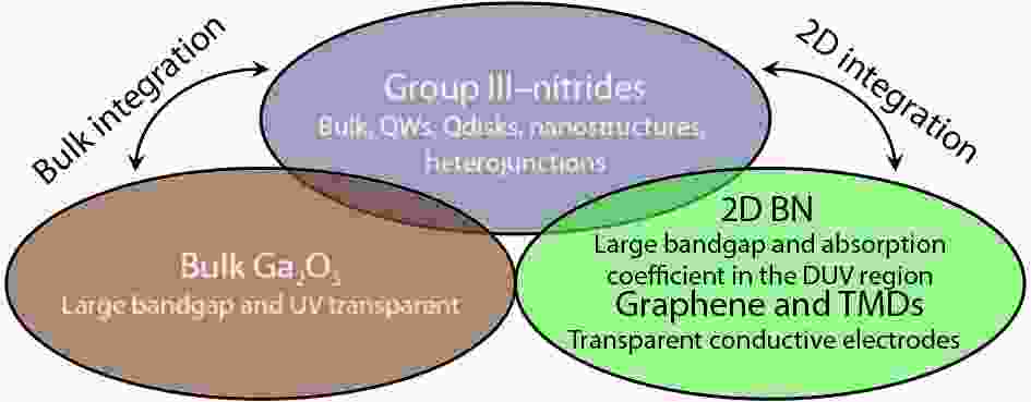
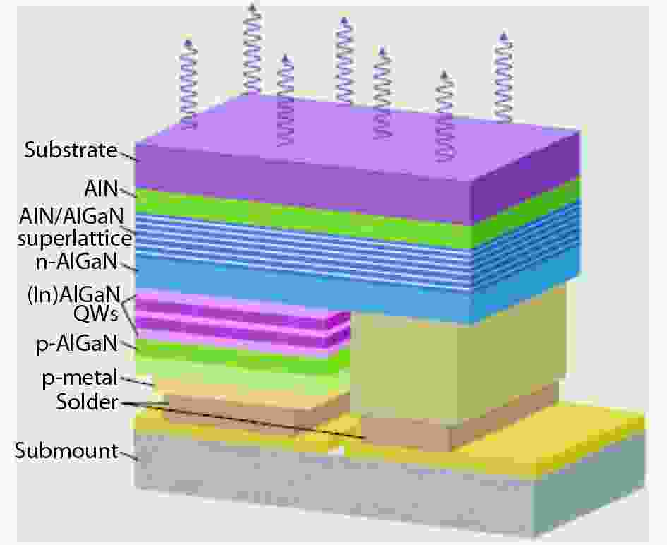
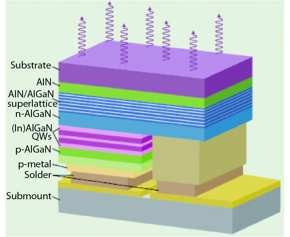
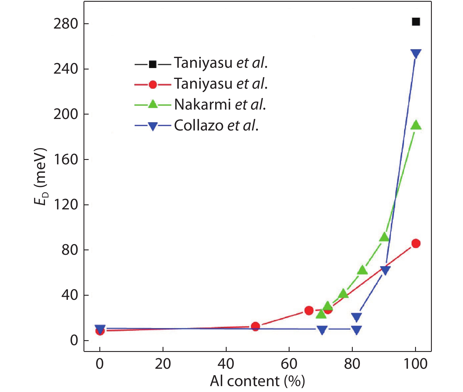
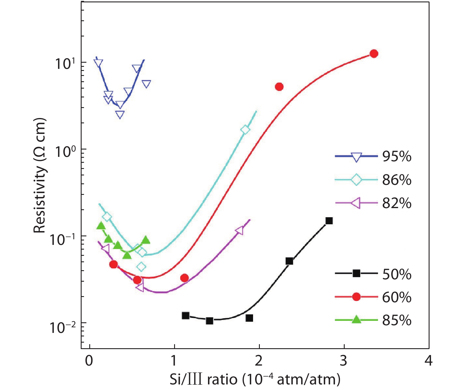
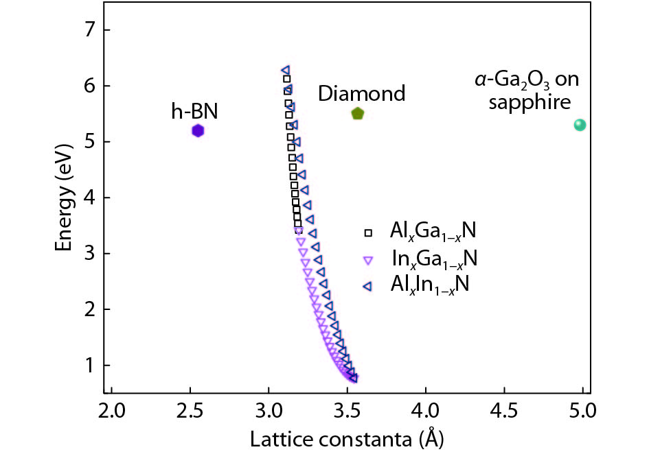
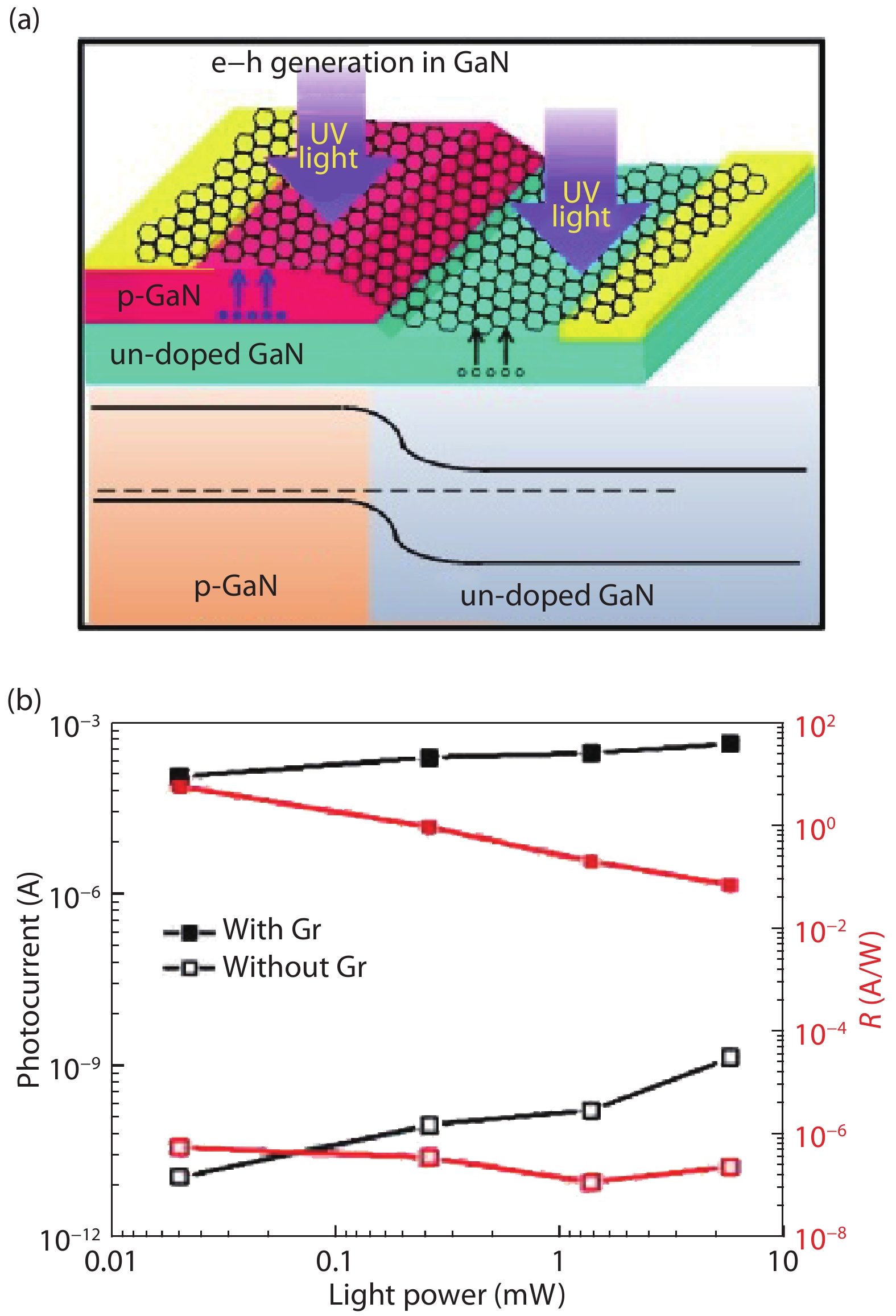
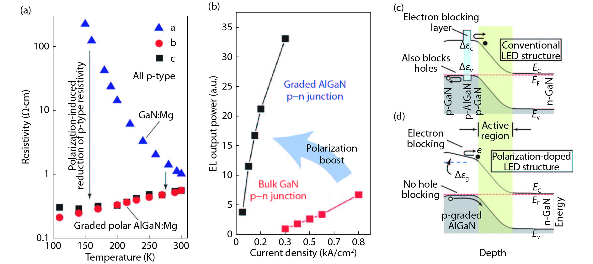
Progress in the design and fabrication of ultraviolet and deep-ultraviolet group III–nitride optoelectronic devices, based on aluminum gallium nitride and boron nitride and their alloys, and the heterogeneous integration with two-dimensional and oxide-based materials is reviewed. We emphasize wide-bandgap nitride compound semiconductors (i.e., (B, Al, Ga)N) as the deep-ultraviolet materials of interest, and two-dimensional materials, namely graphene, two-dimensional boron nitride, and two-dimensional transition metal dichalcogenides, along with gallium oxide, as the hybrid integrated materials. We examine their crystallographic properties and elaborate on the challenges that hinder the realization of efficient and reliable ultraviolet and deep-ultraviolet devices. In this article we provide an overview of aluminum nitride, sapphire, and gallium oxide as platforms for deep-ultraviolet optoelectronic devices, in which we criticize the status of sapphire as a platform for efficient deep-ultraviolet devices and detail advancements in device growth and fabrication on aluminum nitride and gallium oxide substrates. A critical review of the current status of deep-ultraviolet light emission and detection materials and devices is provided.


J. Semicond.
2019, 40(12): 121802 doi: 10.1088/1674-4926/40/12/121802
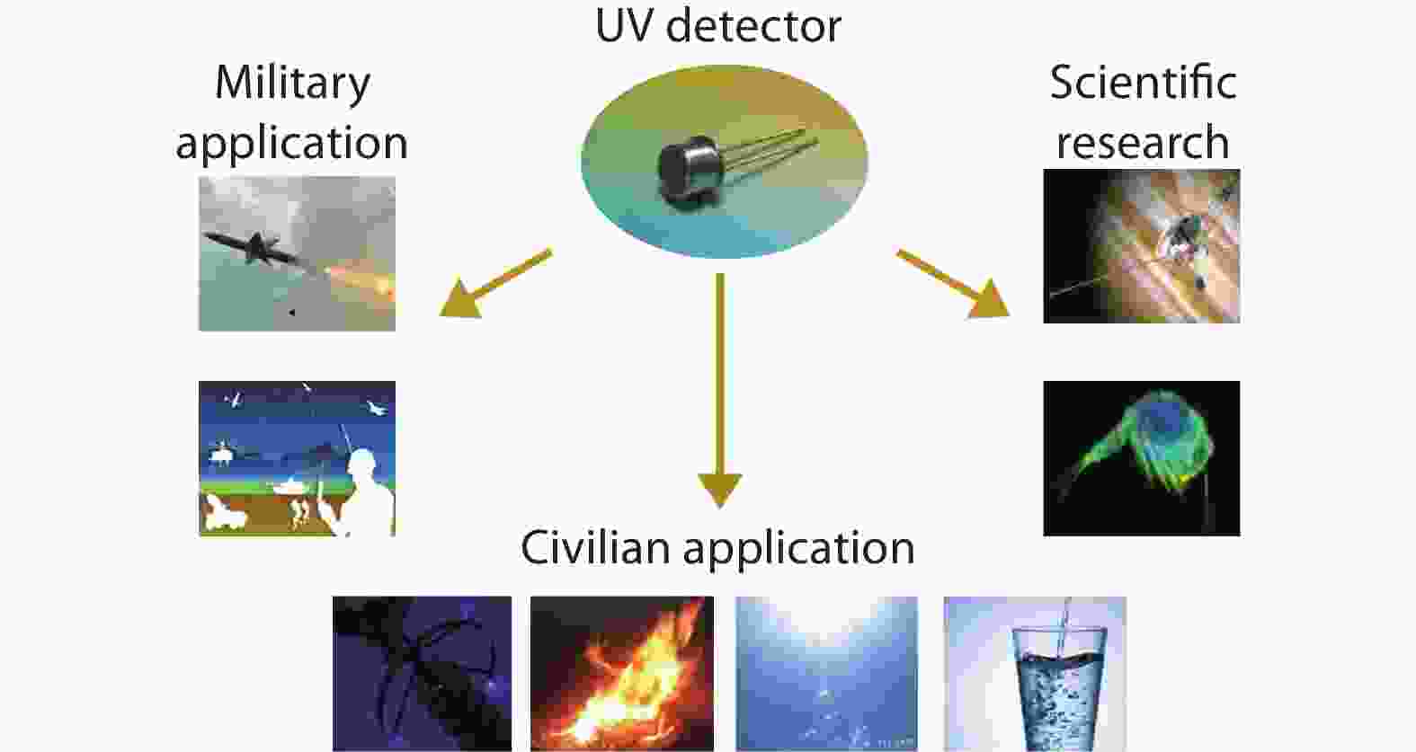
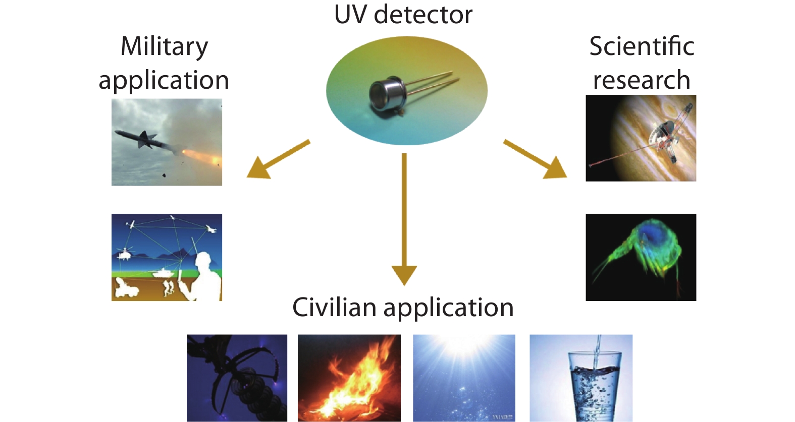
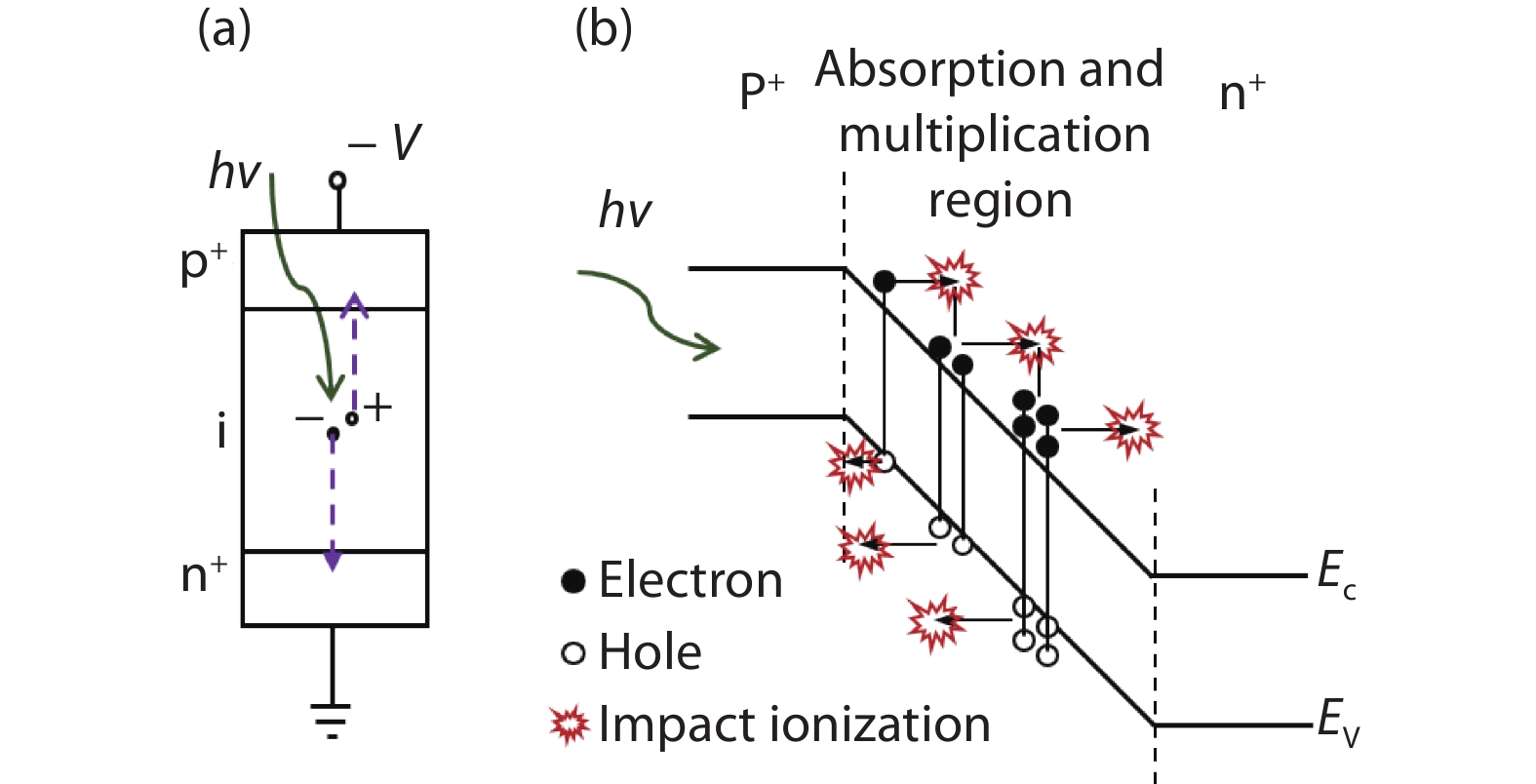
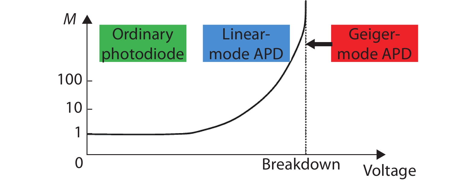
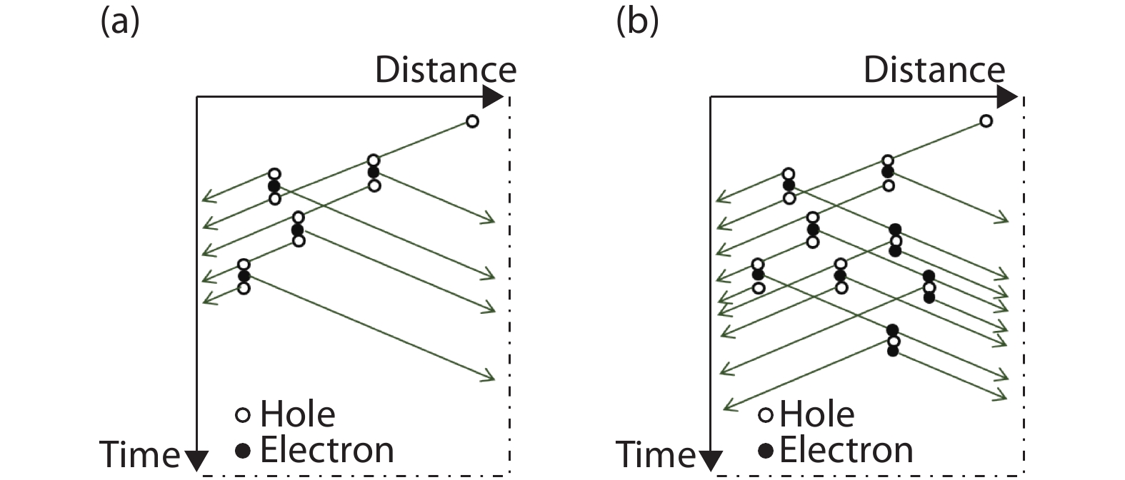
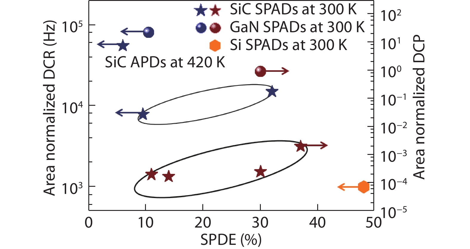
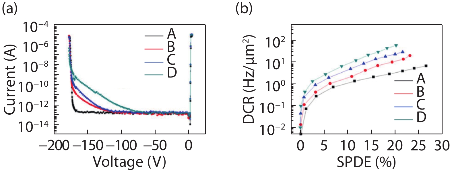
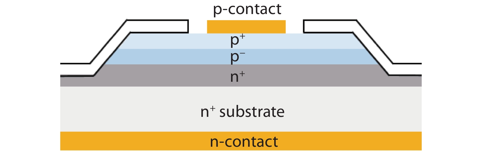
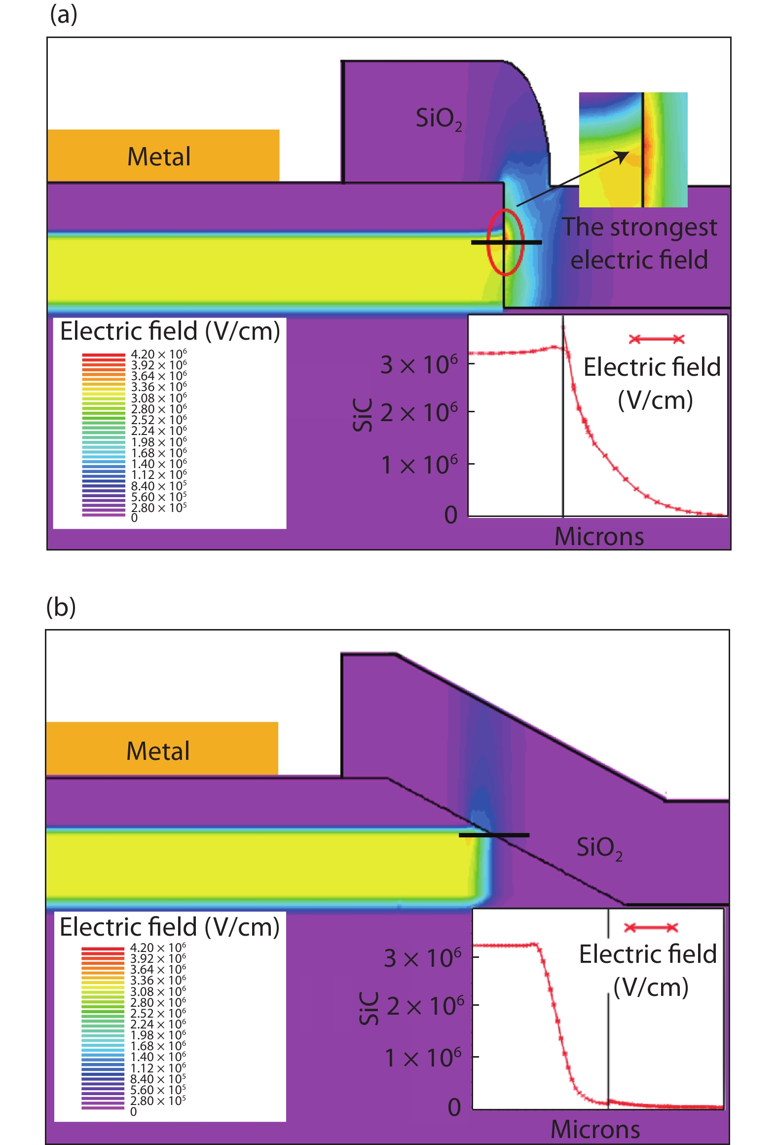
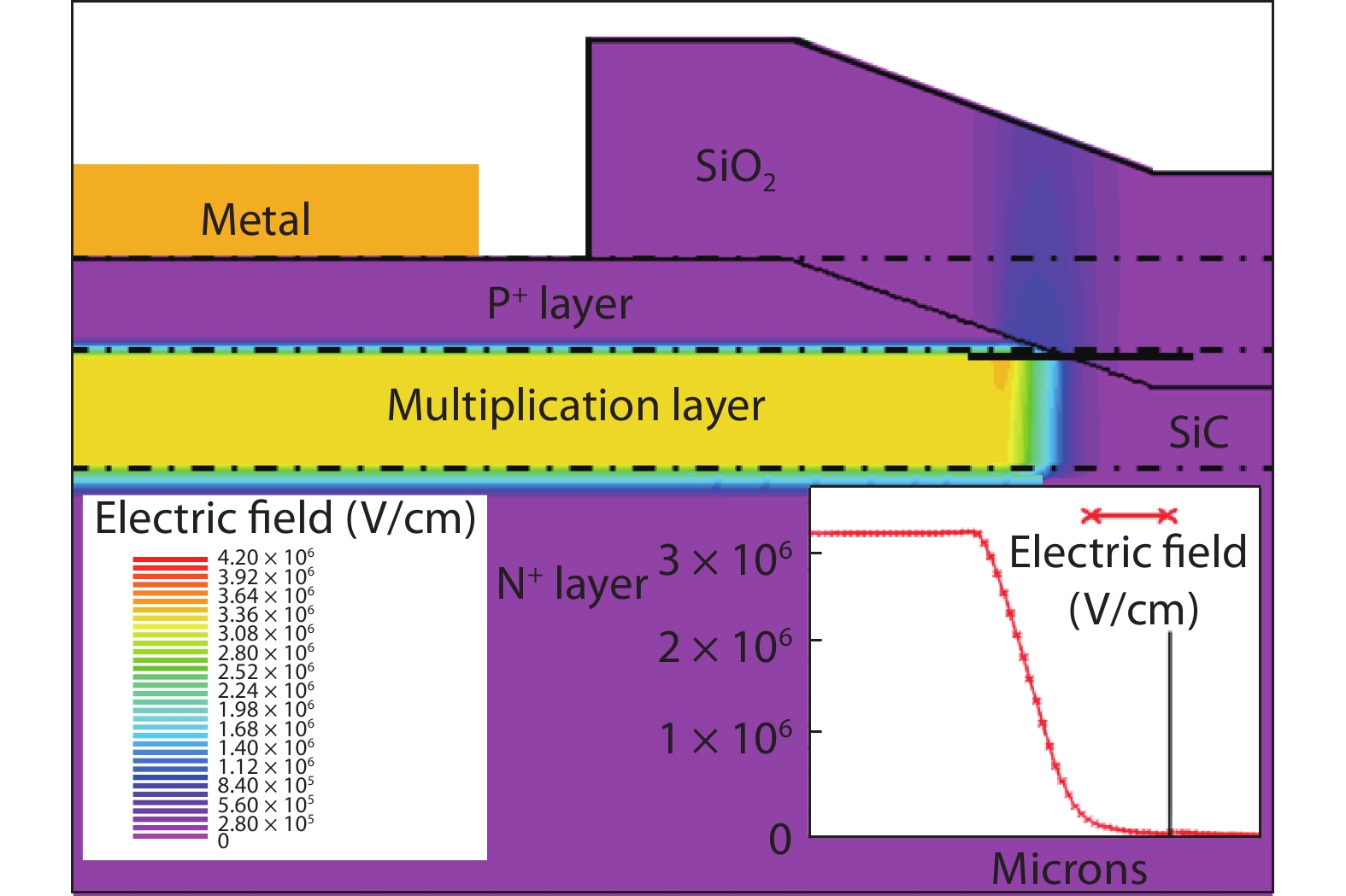
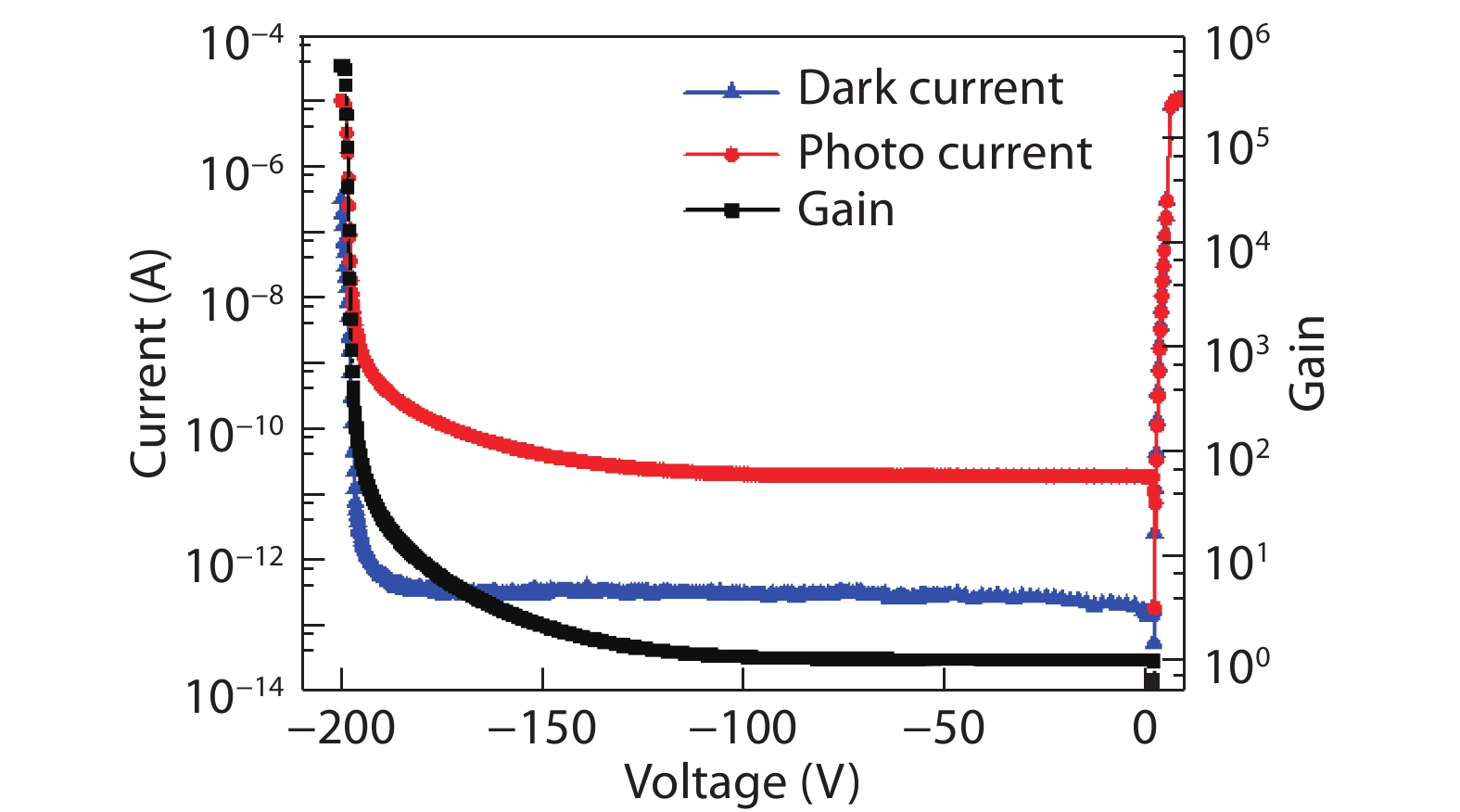
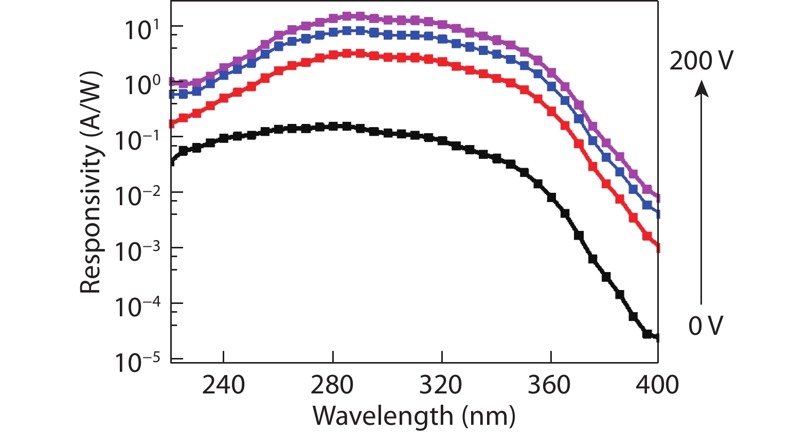
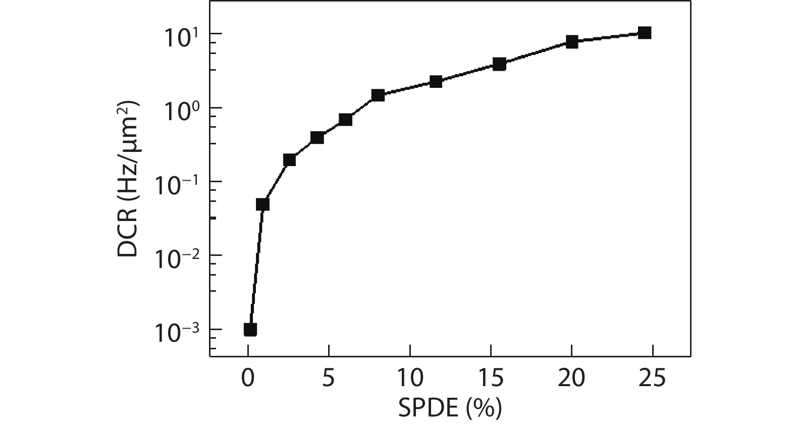
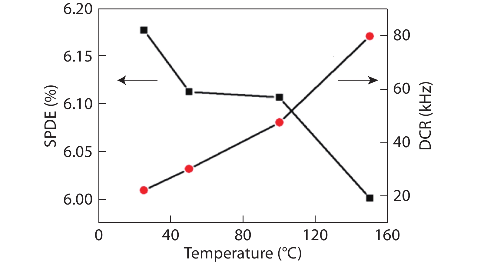
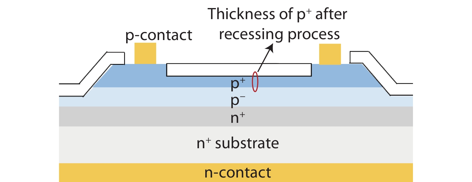
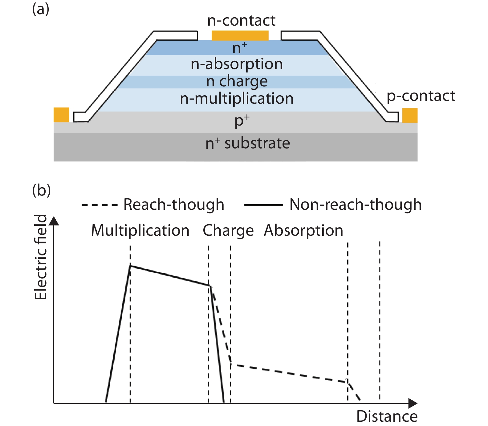
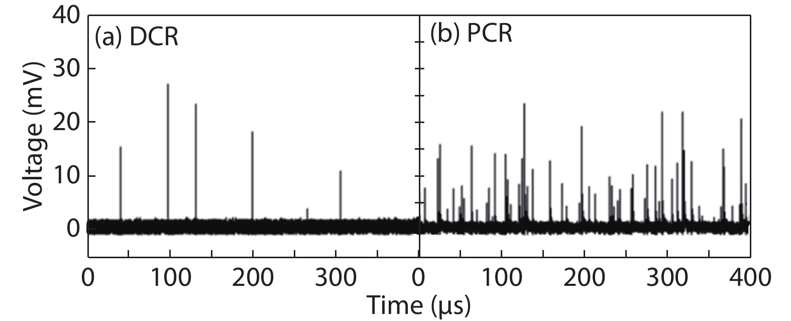
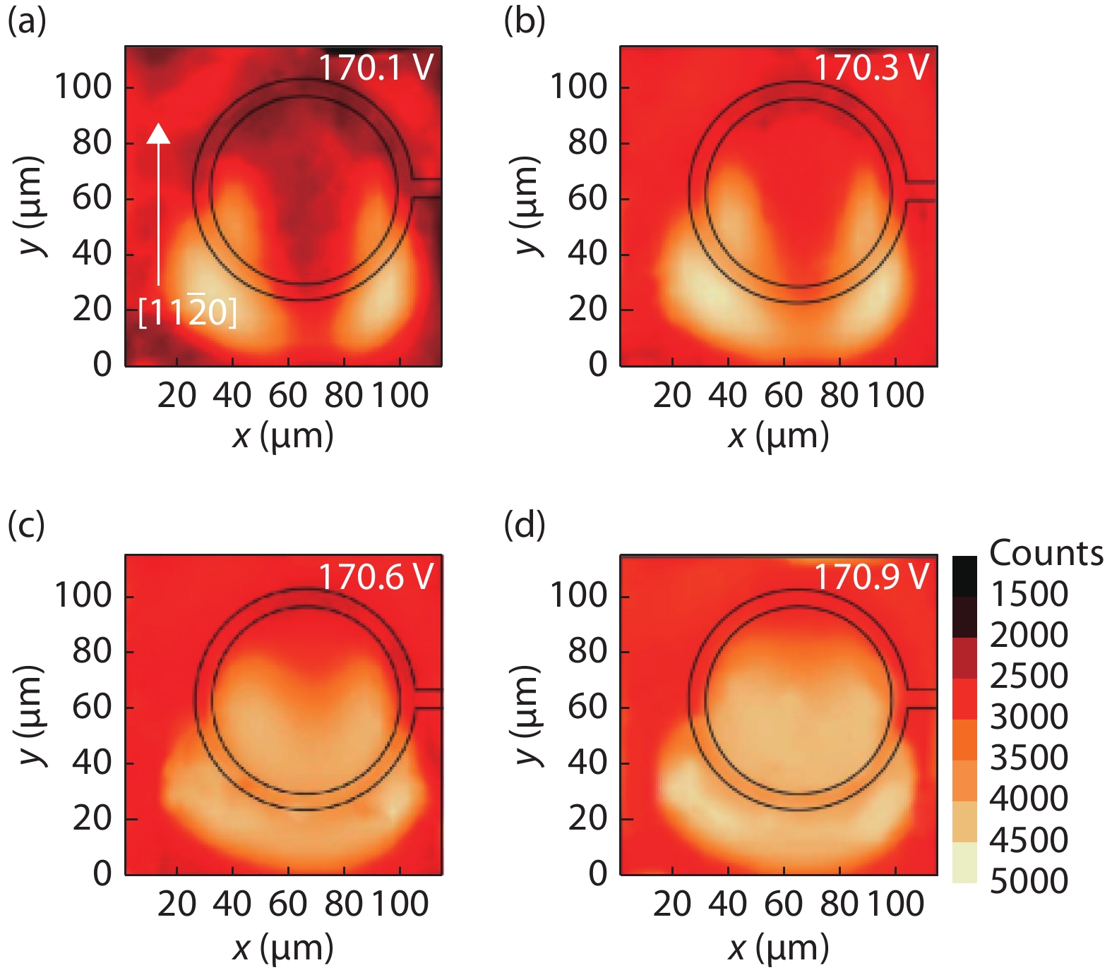
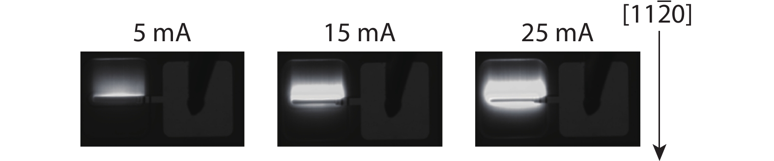
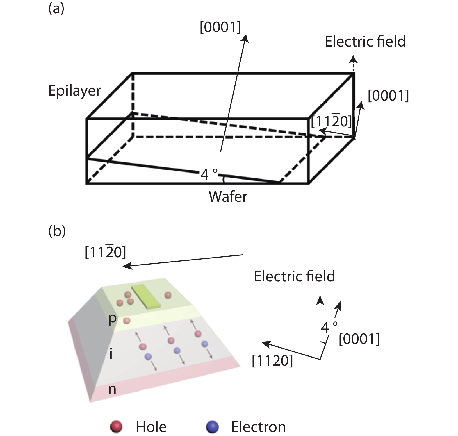
4H-SiC single photon counting avalanche photodiodes (SPADs) are prior devices for weak ultraviolet (UV) signal detection with the advantages of small size, low leakage current, high avalanche multiplication gain, and high quantum efficiency, which benefit from the large bandgap energy, high carrier drift velocity and excellent physical stability of 4H-SiC semiconductor material. UV detectors are widely used in many key applications, such as missile plume detection, corona discharge, UV astronomy, and biological and chemical agent detection. In this paper, we will describe basic concepts and review recent results on device design, process development, and basic characterizations of 4H-SiC avalanche photodiodes. Several promising device structures and uniformity of avalanche multiplication are discussed, which are important for achieving high performance of 4H-SiC UV SPADs.


J. Semicond.
2019, 40(12): 121803 doi: 10.1088/1674-4926/40/12/121803
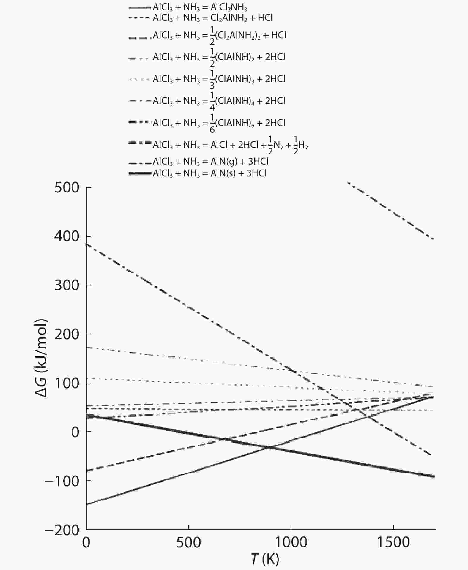
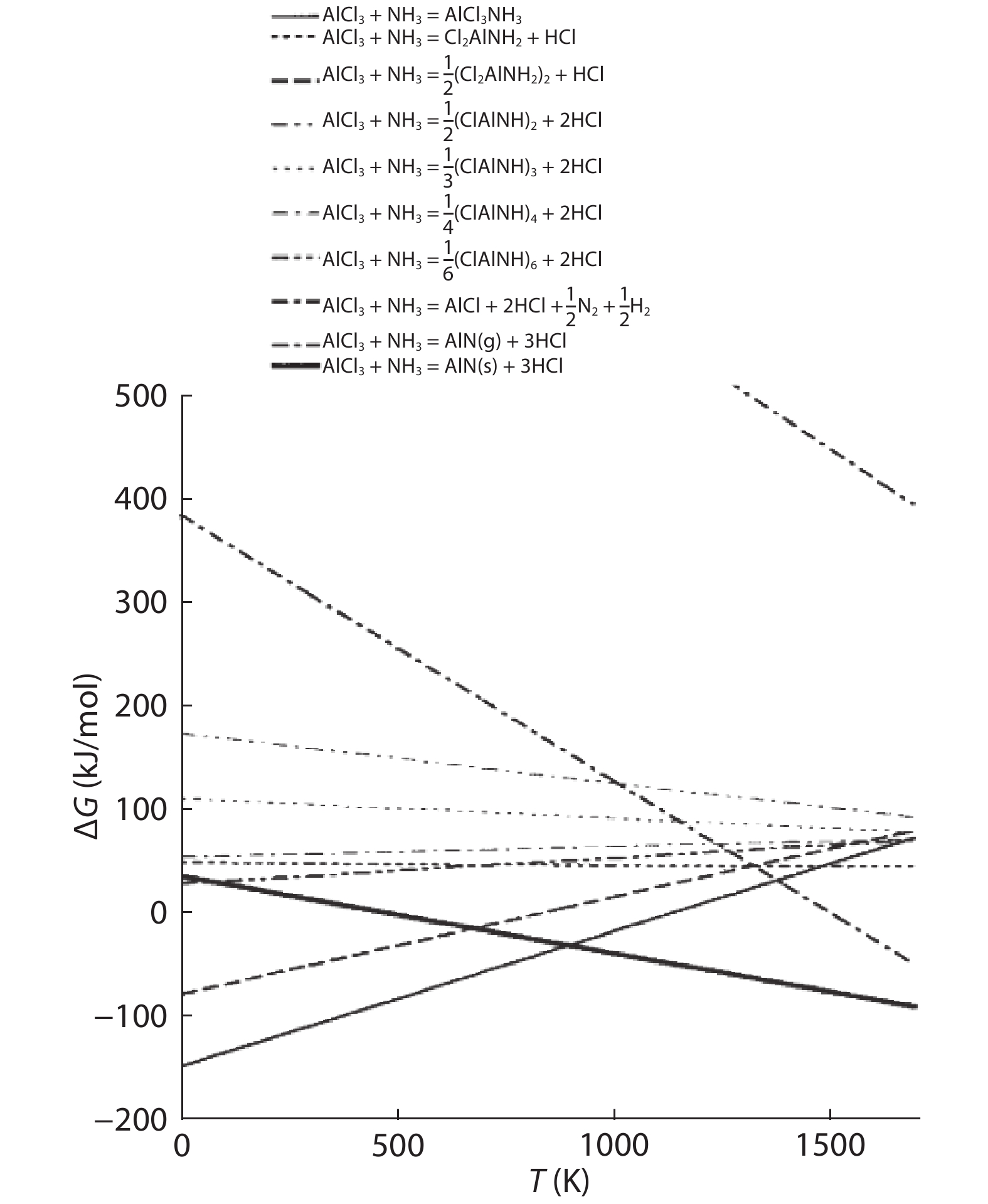
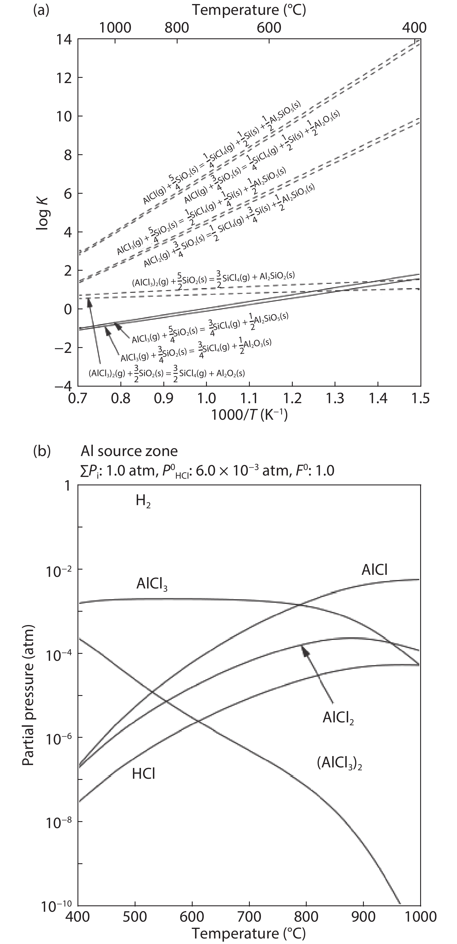
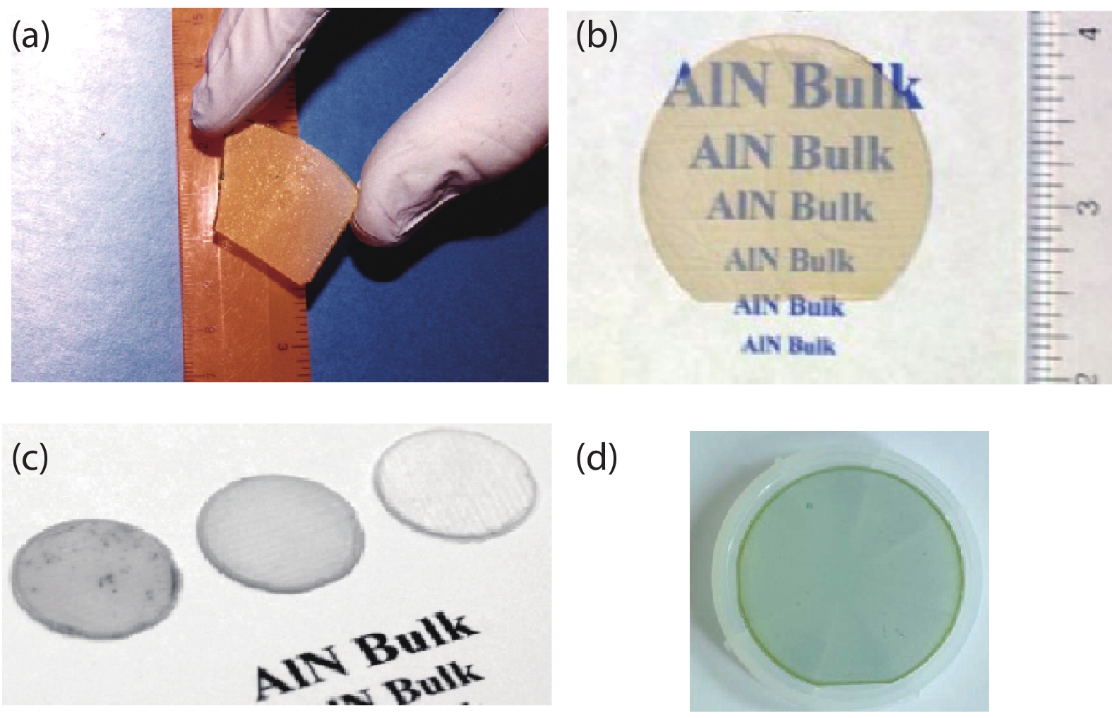
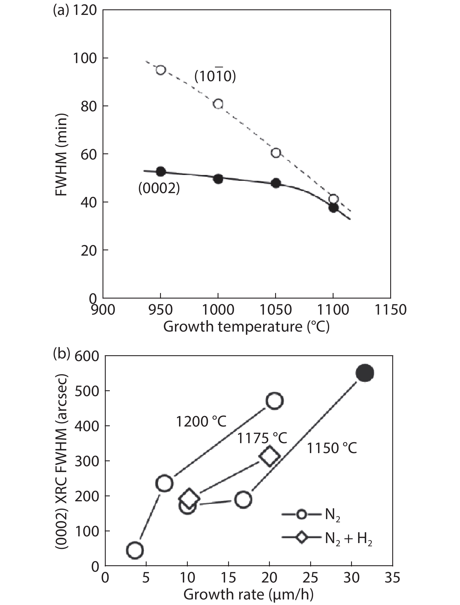
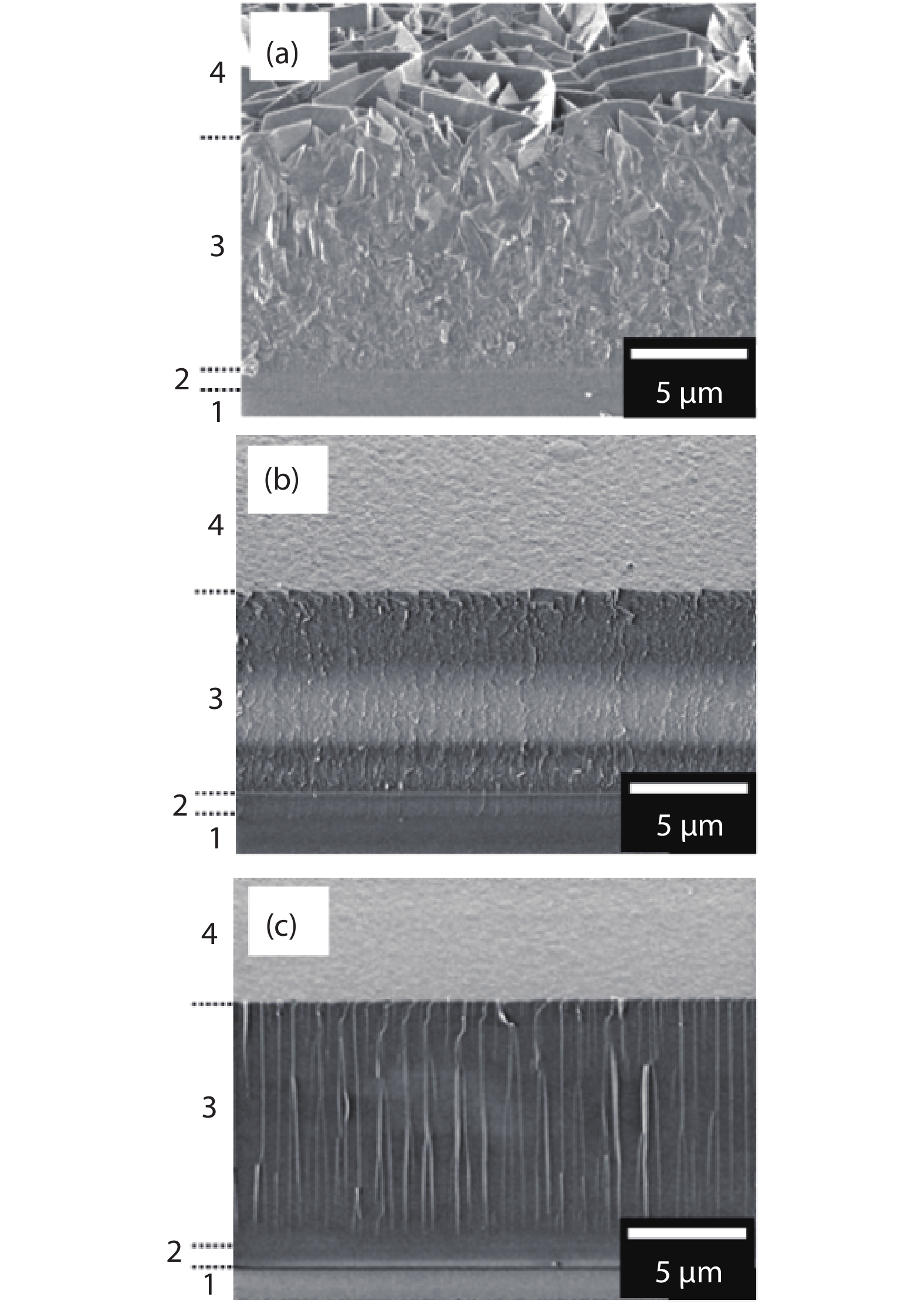
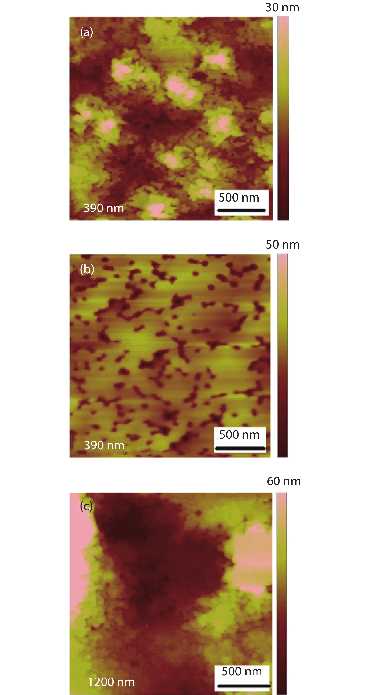
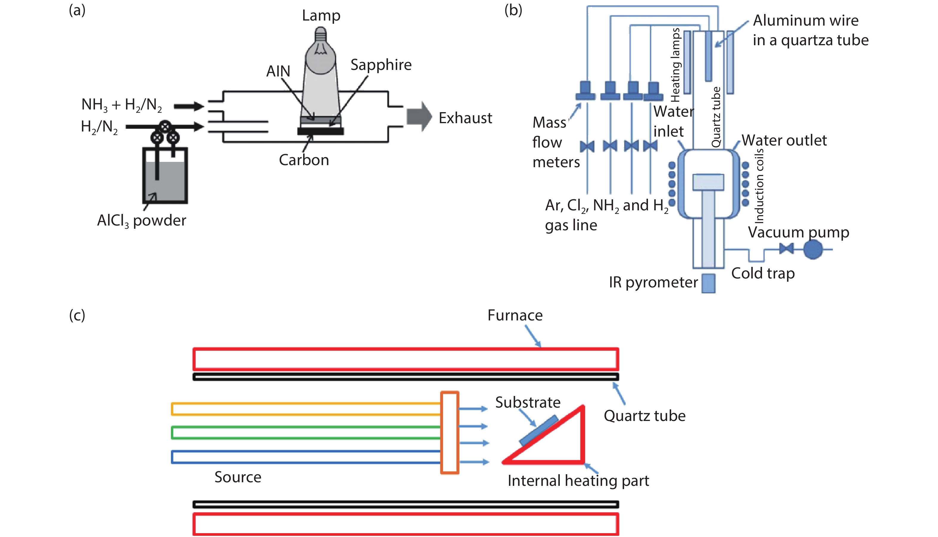
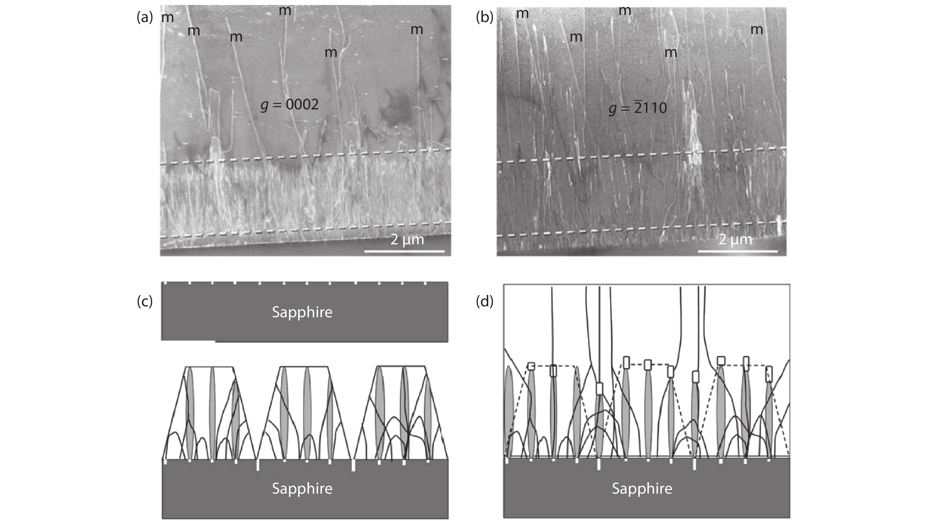
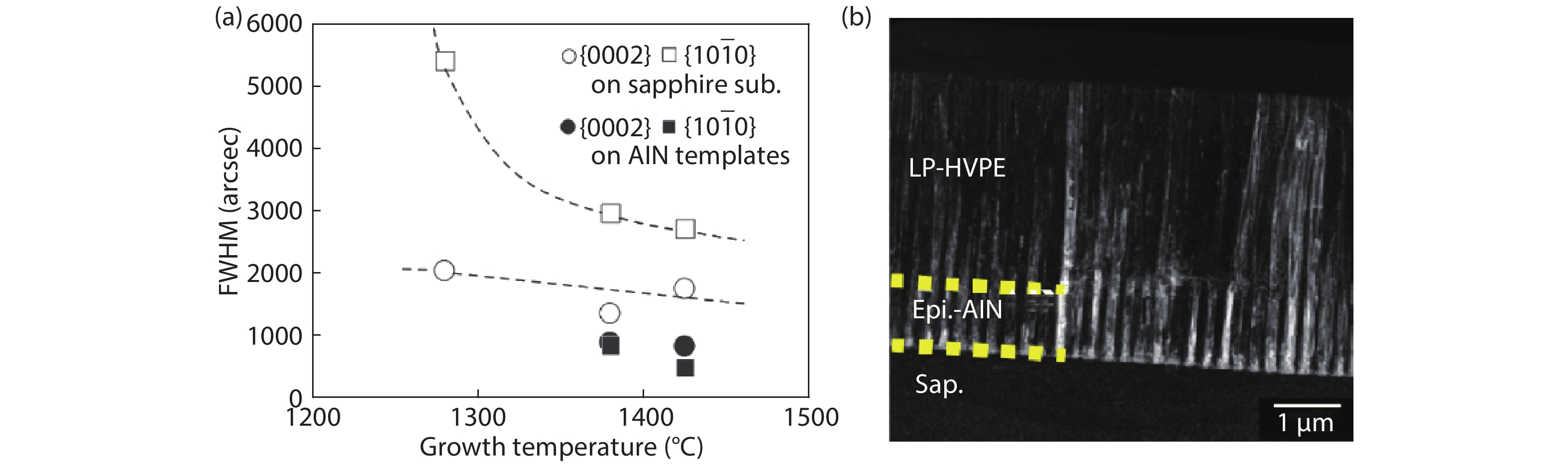
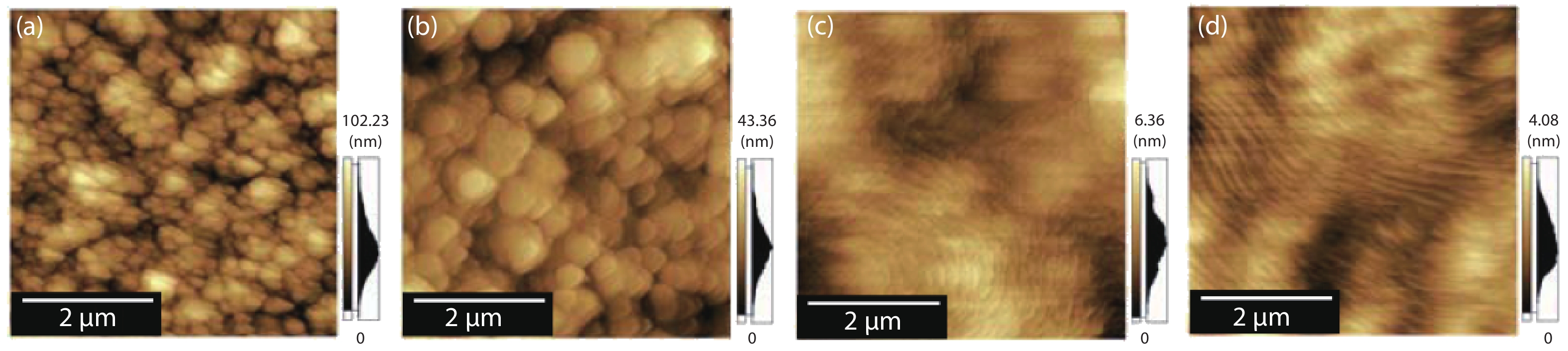
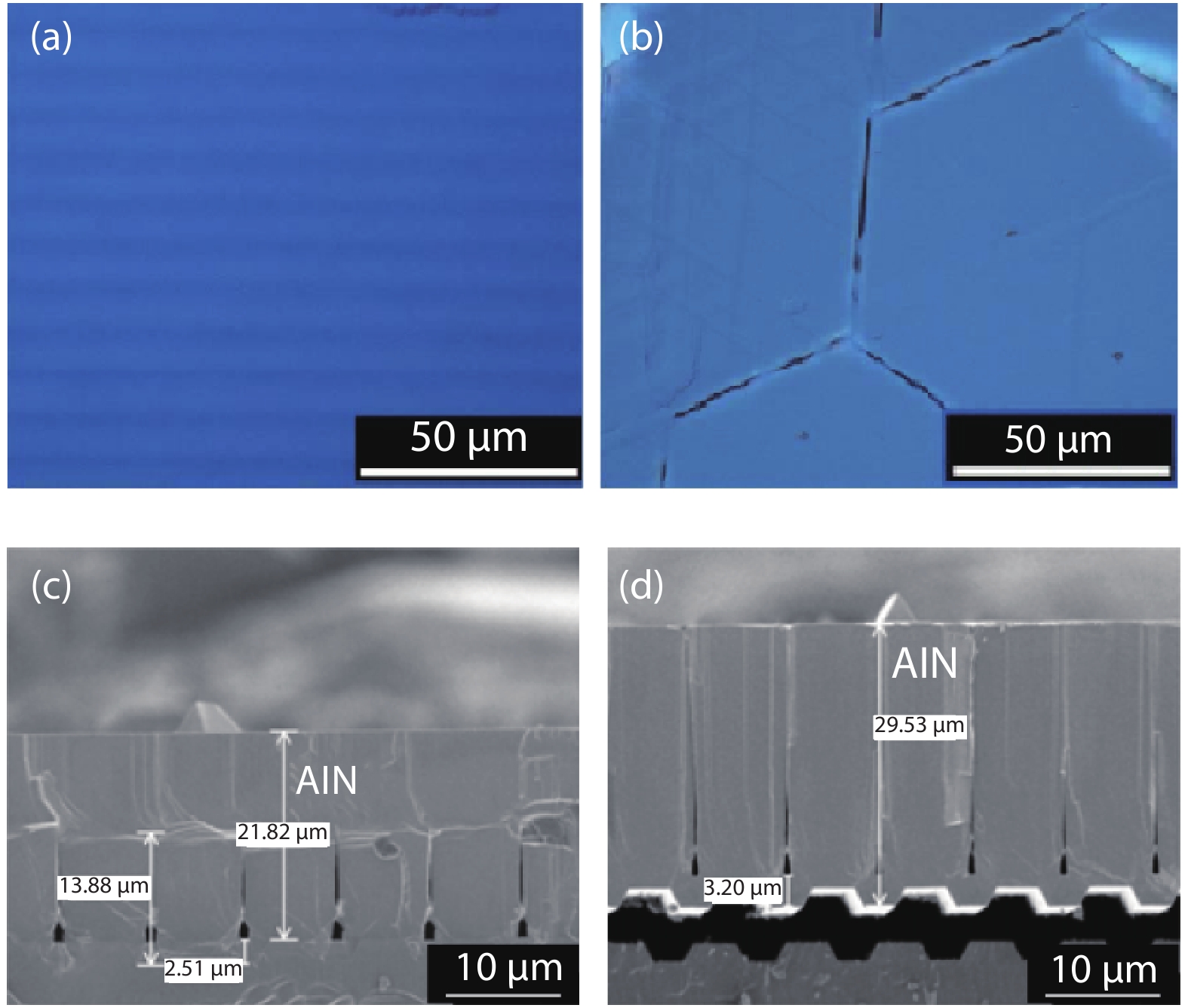
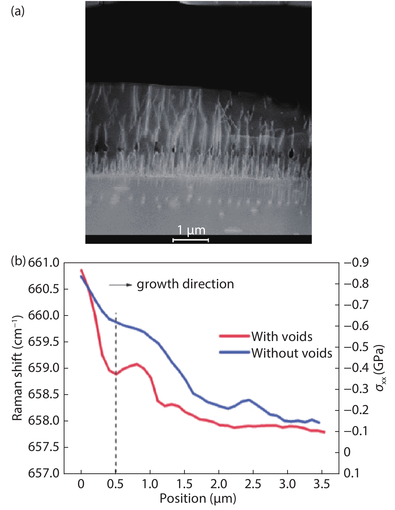
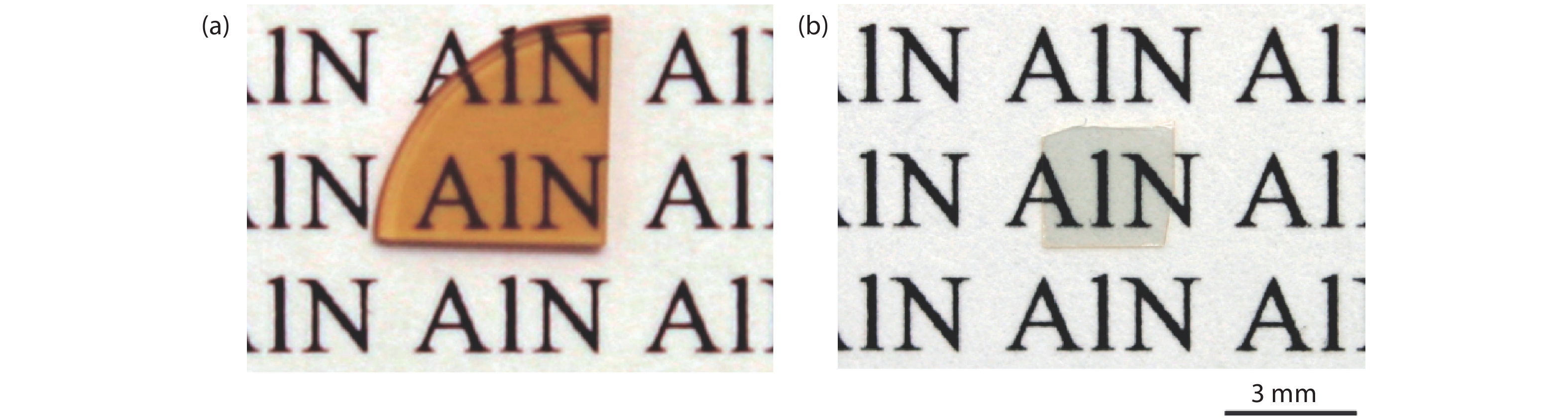
Aluminum nitride (AlN) is the promising substrates material for the epitaxial growth of III-nitrides devices, such as high-power, high-frequency electronic, deep ultraviolet optoelectronics and acoustic devices. However, it is rather difficult to obtain the high quality and crack-free thick AlN wafers because of the low surface migration of Al adatoms and the large thermal and lattice mismatches between the foreign substrates and AlN. In this work, the fabrication of AlN material by hydride vapor phase epitaxy (HVPE) was summarized and discussed. At last, the outlook of the production of AlN by HVPE was prospected.


J. Semicond.
2019, 40(12): 122801 doi: 10.1088/1674-4926/40/12/122801
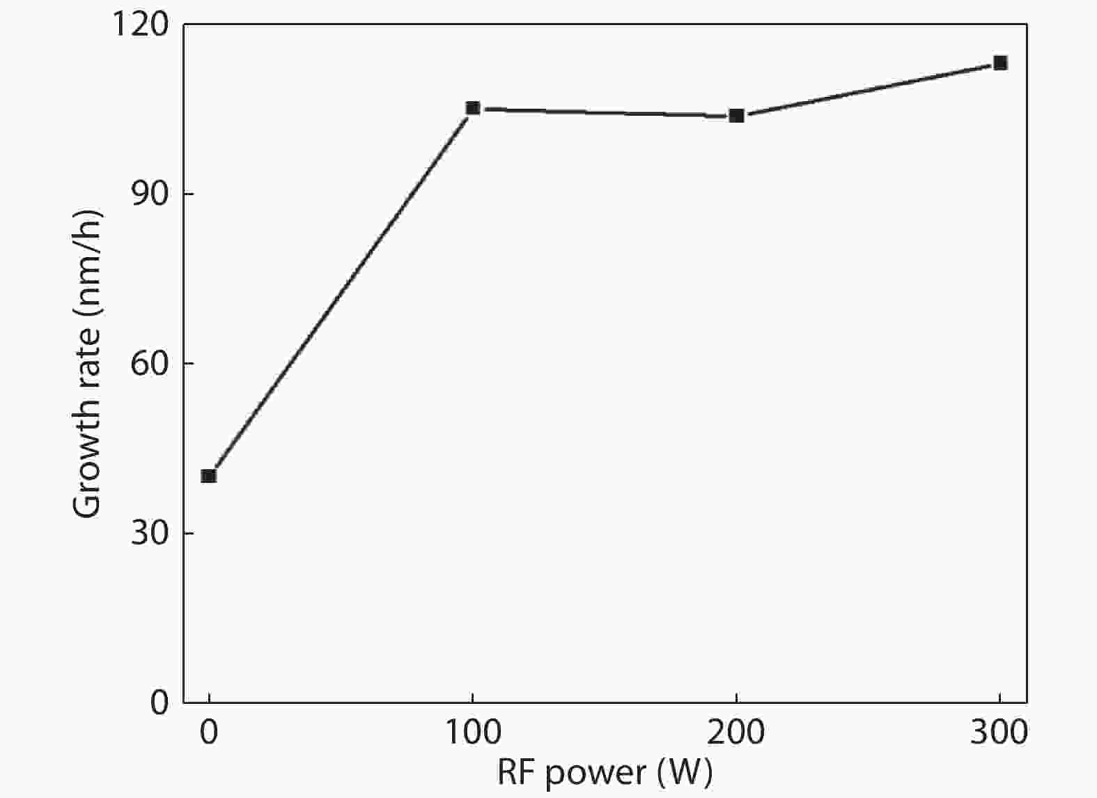
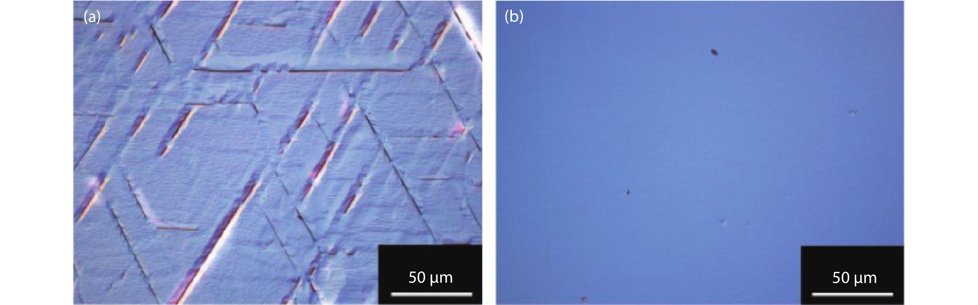
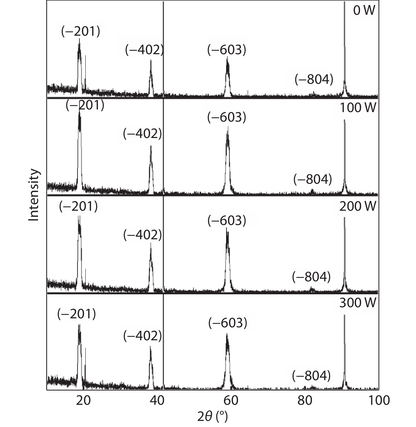
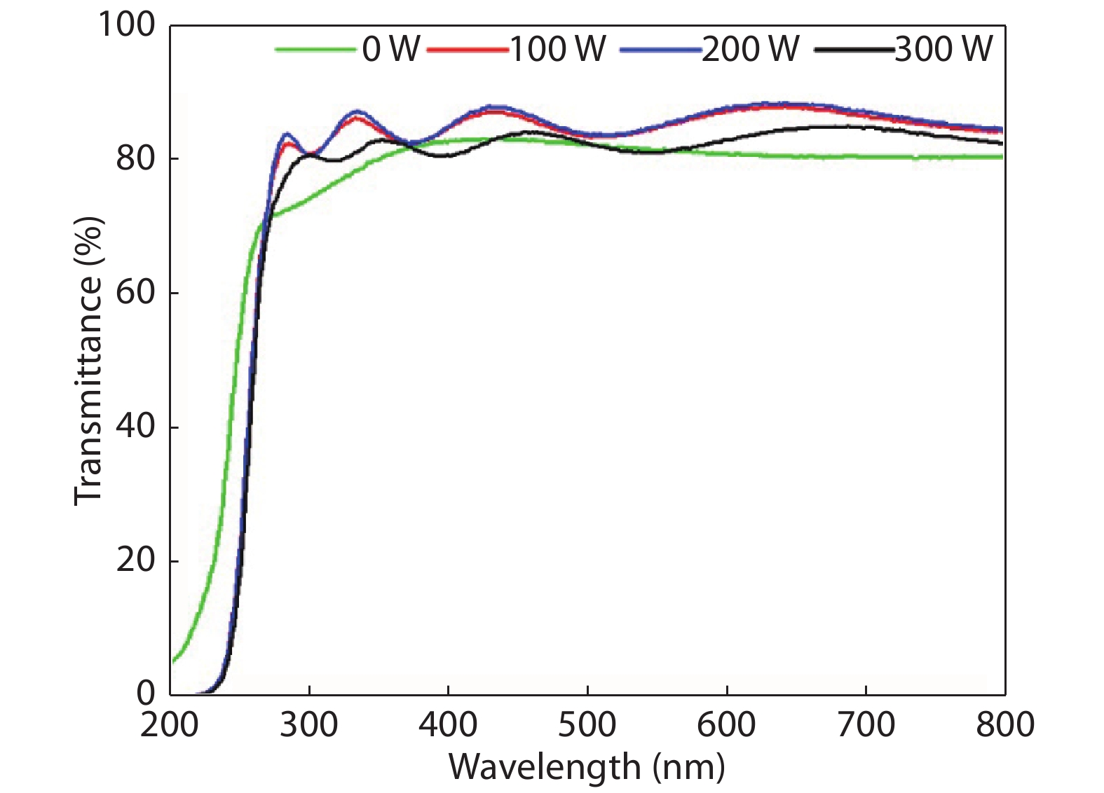
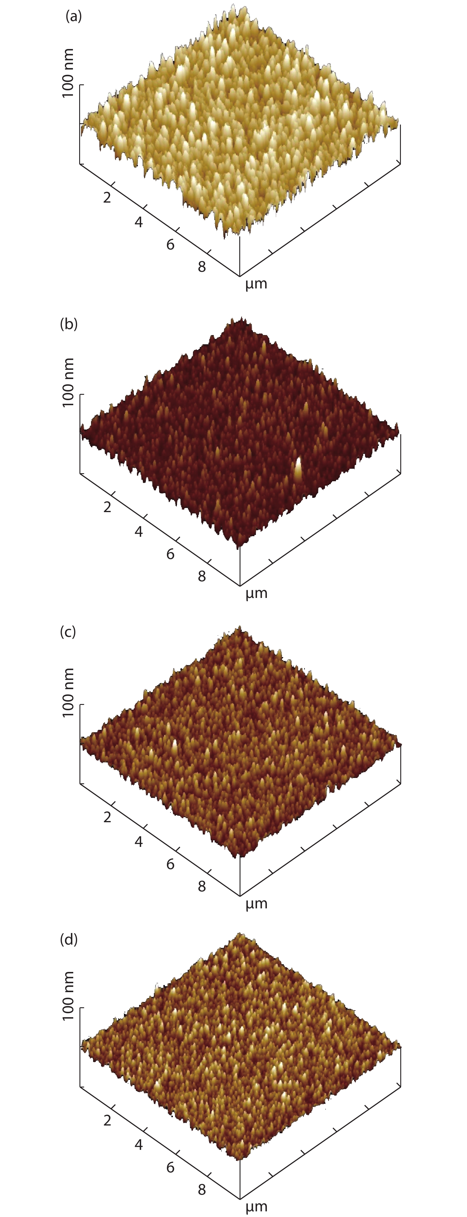
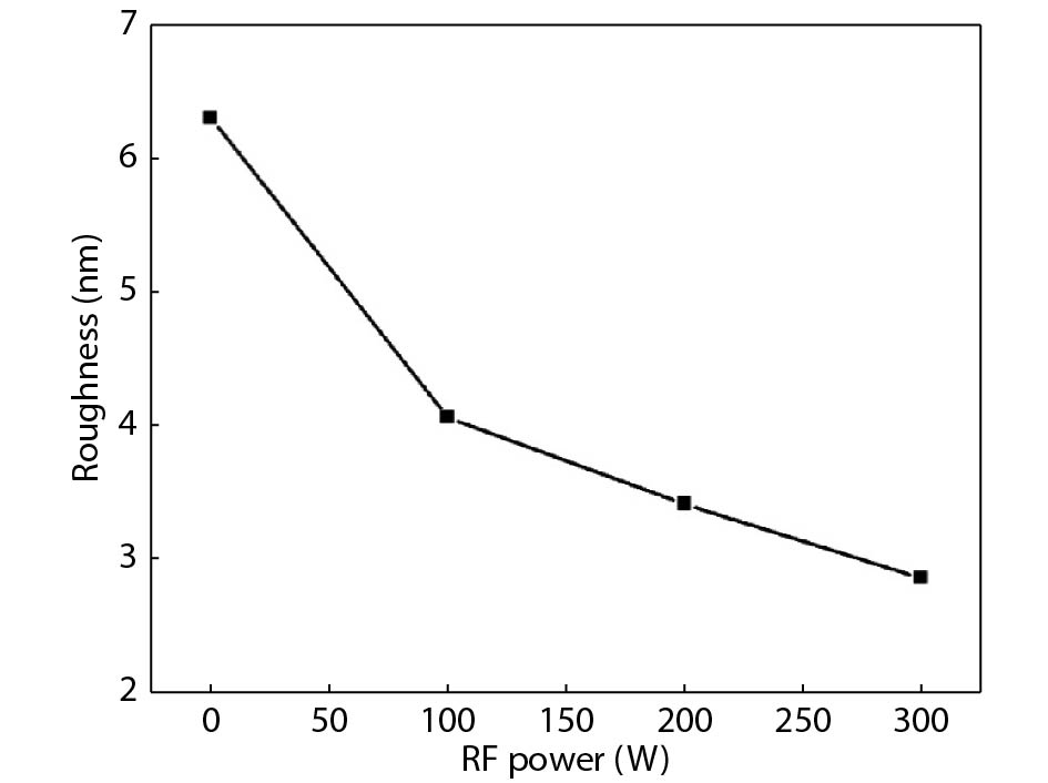
Gallium oxide was deposited on a c-plane sapphire substrate by oxygen plasma-assisted pulsed laser deposition (PLD). An oxygen radical was generated by an inductive coupled plasma source and the effect of radio frequency (RF) power on growth rate was investigated. A film grown with plasma assistance showed 2.7 times faster growth rate. X-ray diffraction and Raman spectroscopy analysis showed β-Ga2O3 films grown with plasma assistance at 500 °C. The roughness of the films decreased when the RF power of plasma treatment increased. Transmittance of these films was at least 80% and showed sharp absorption edge at 250 nm which was consistent with data previously reported.


J. Semicond.
2019, 40(12): 122802 doi: 10.1088/1674-4926/40/12/122802
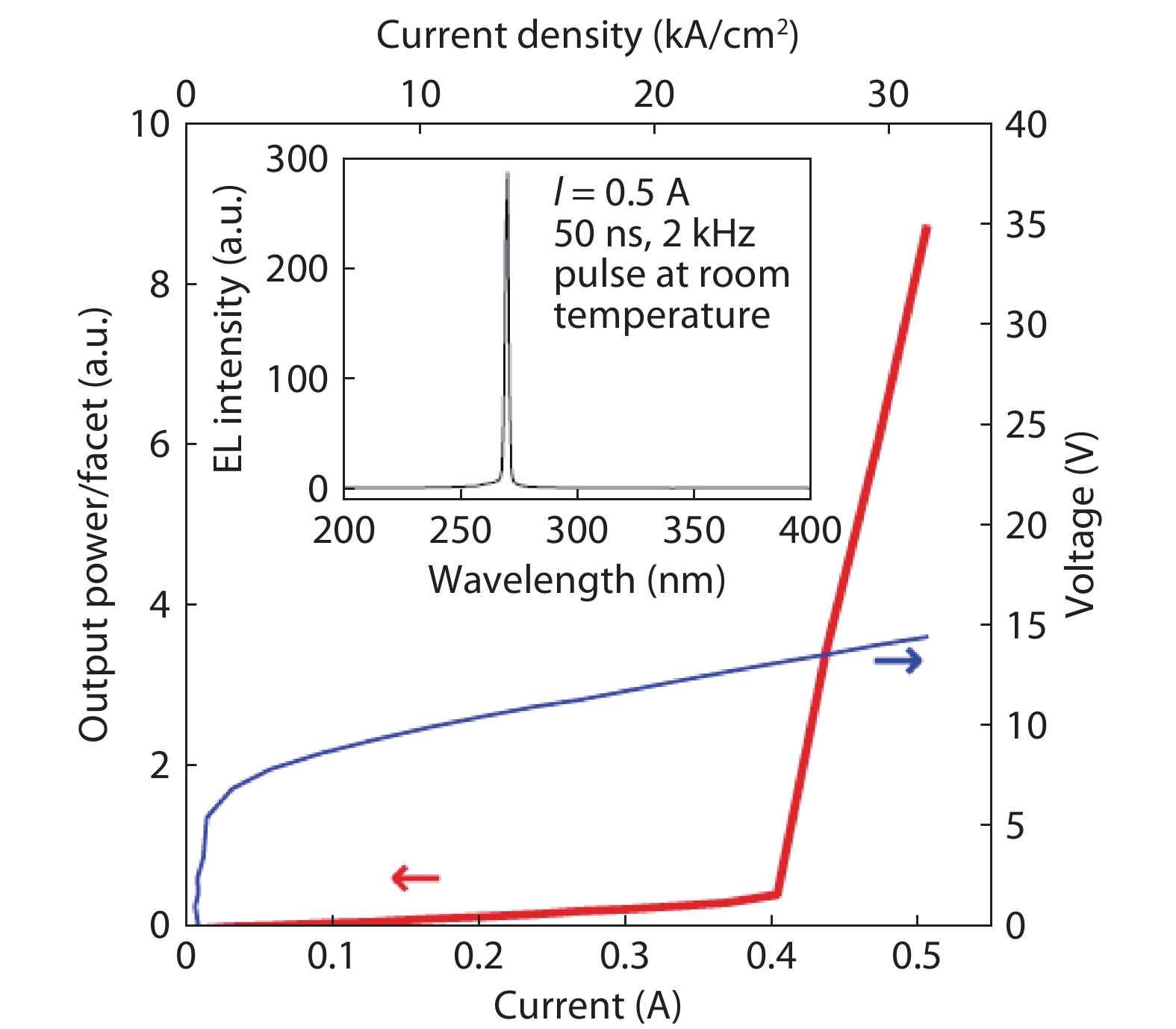
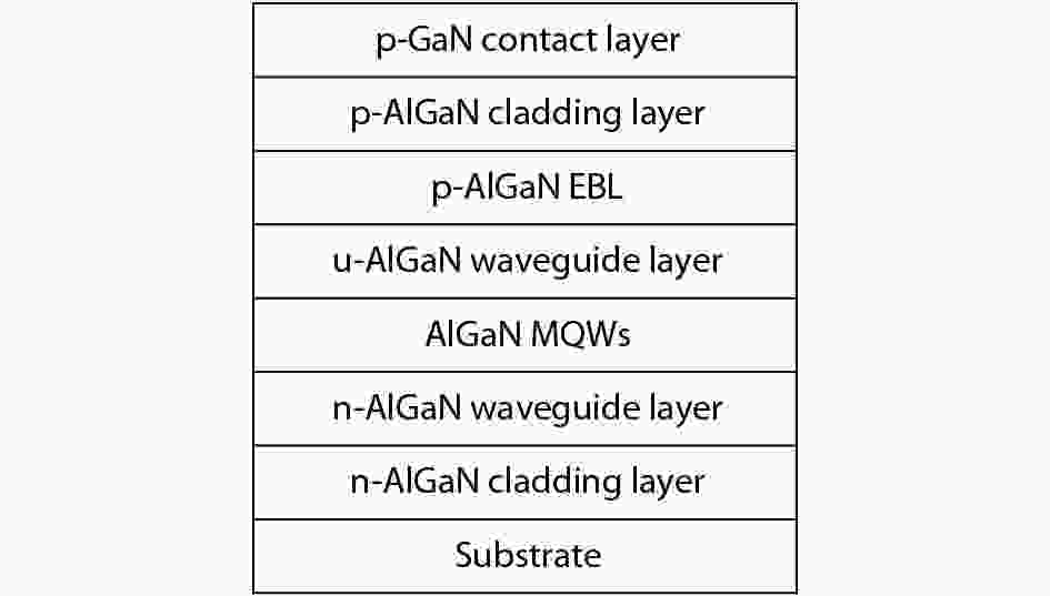
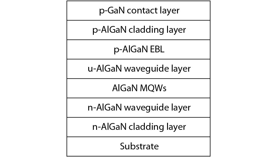
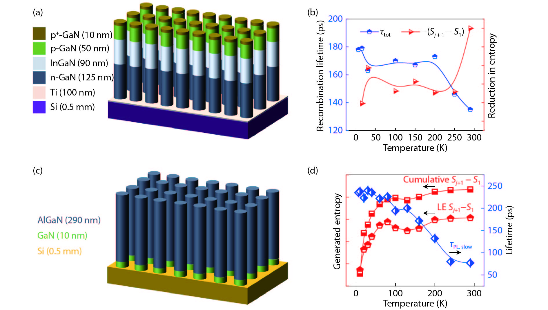
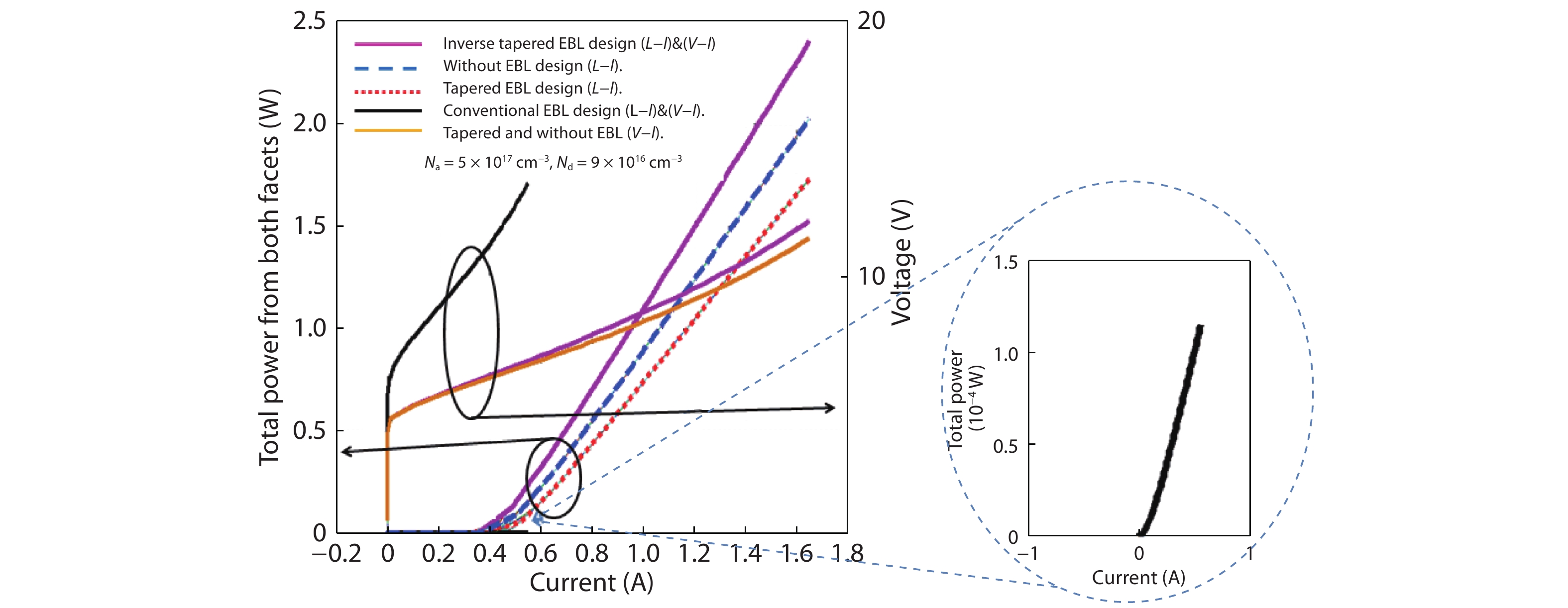
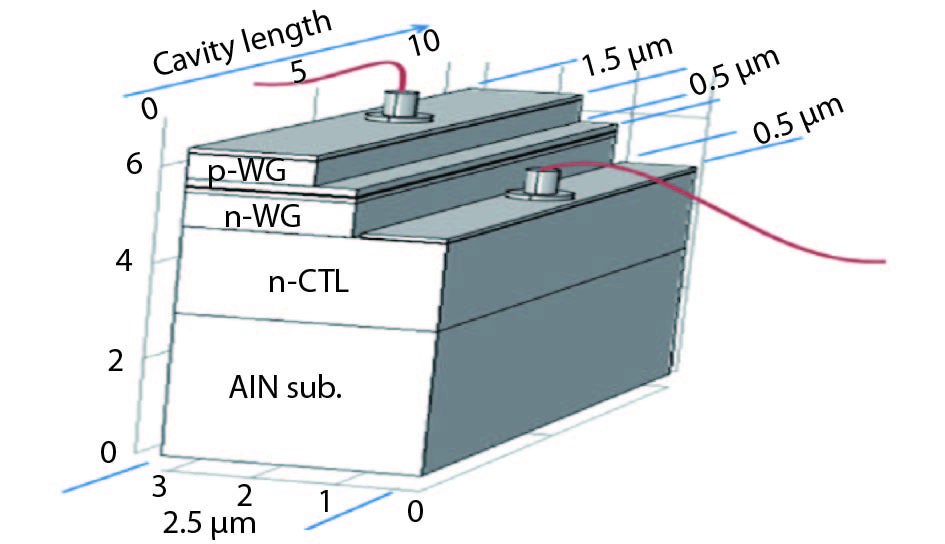
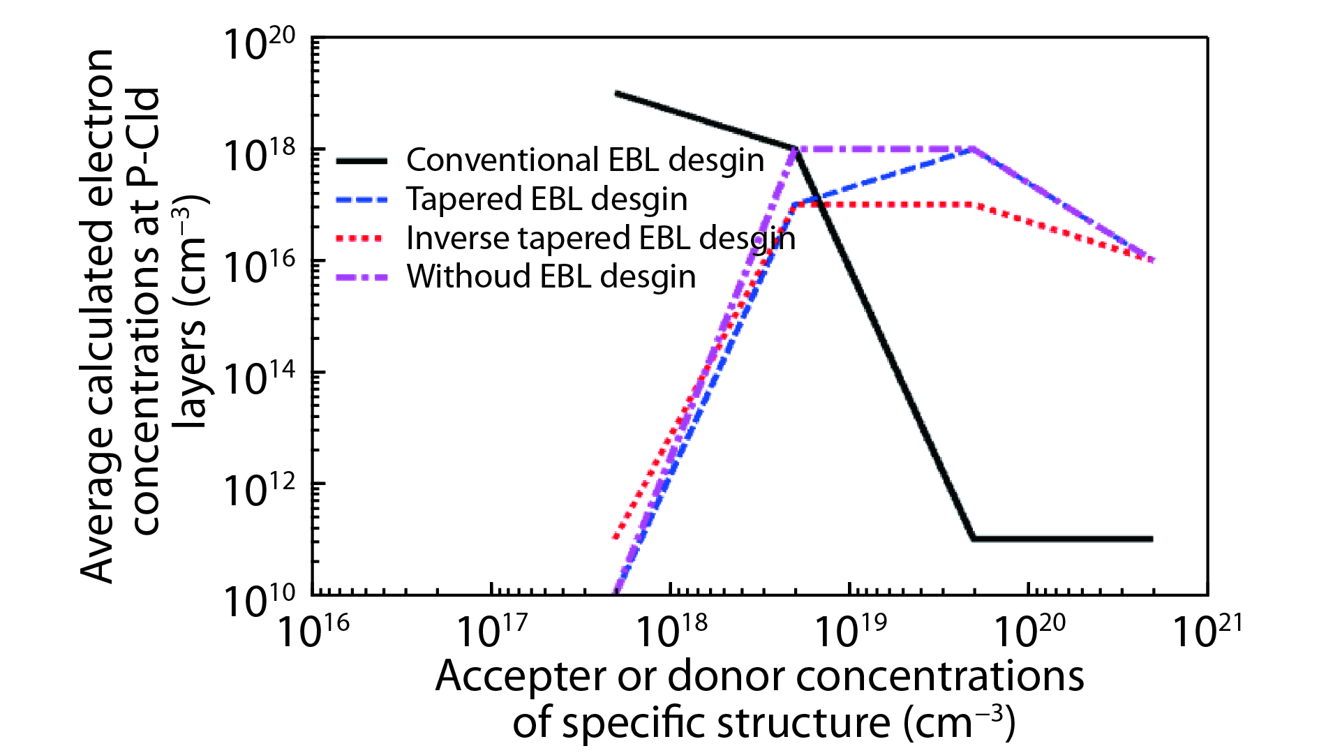
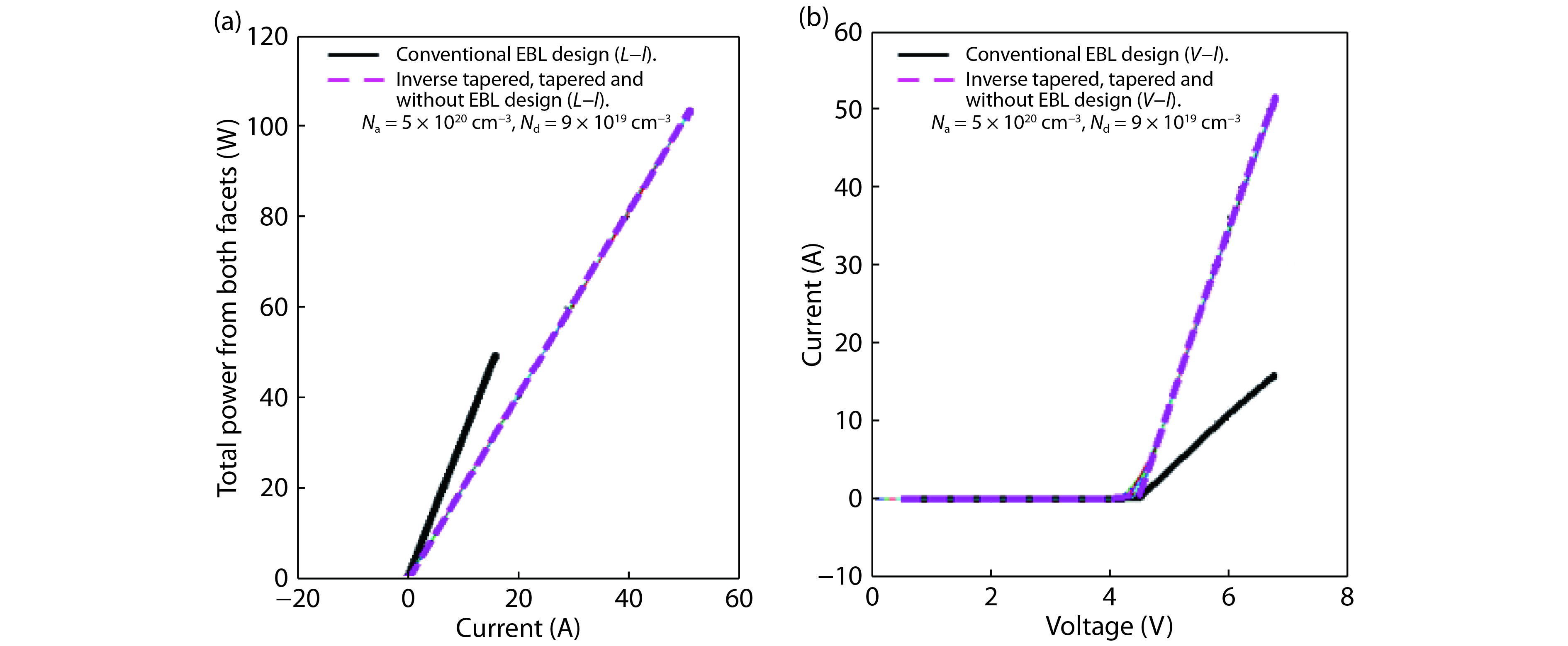
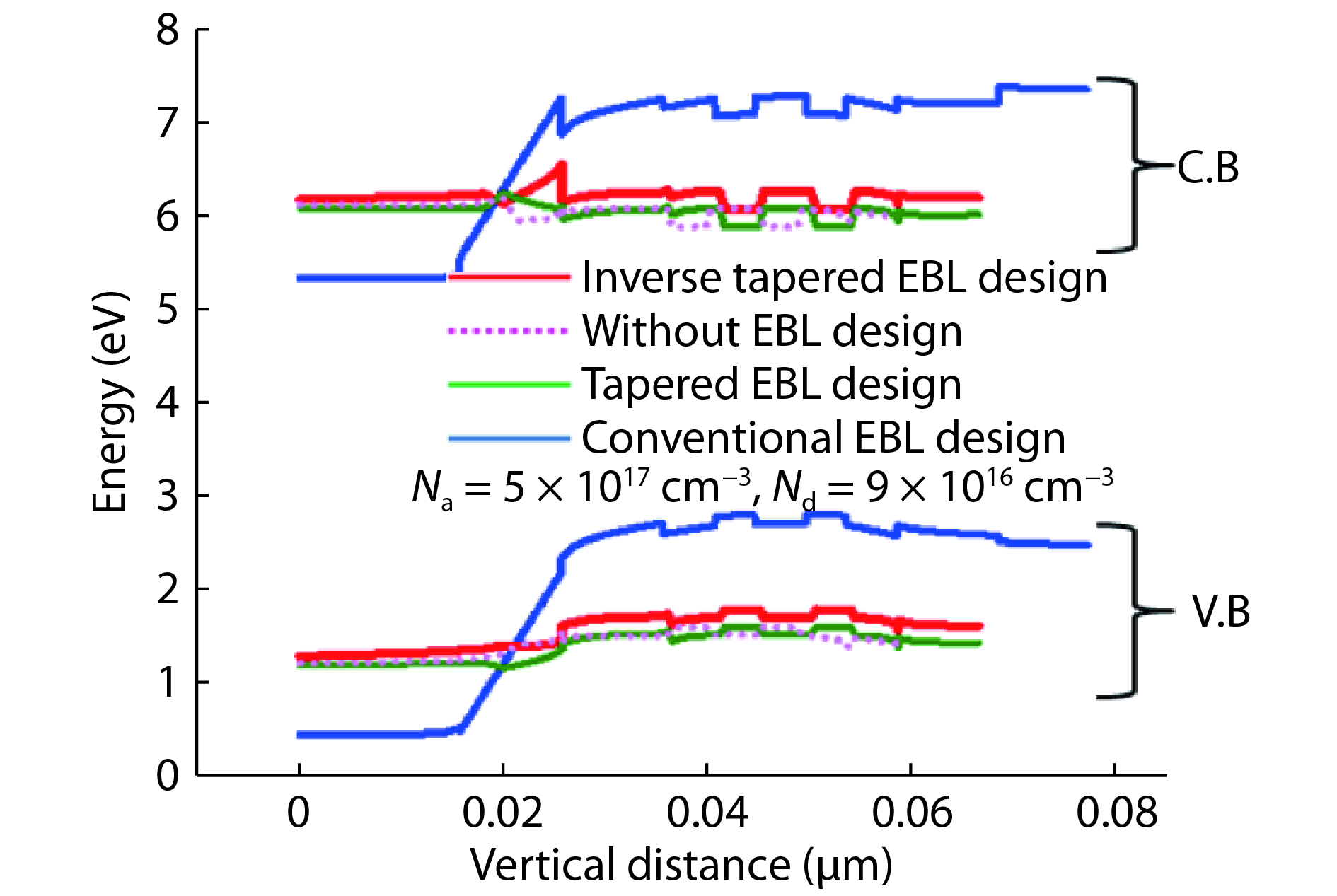
In this paper, an ultraviolet C-band laser diode lasing at 277 nm composed of B0.313Ga0.687N/B0.40Ga0.60N QW/QB heterostructure on Mg and Si-doped AlxGa1–xN layers was designed, as well as a lowest reported substitutional accepter and donor concentration up to NA = 5.0 × 1017 cm–3 and ND = 9.0 × 1016 cm–3 for deep ultraviolet lasing was achieved. The structure was assumed to be grown over bulk AlN substrate and operate under a continuous wave at room temperature. Although there is an emphasizing of the suitability for using boron nitride wide band gap in the deep ultraviolet region, there is still a shortage of investigation about the ternary BGaN in aluminum-rich AlGaN alloys. Based on the simulation, an average local gain in quantum wells of 1946 cm–1, the maximum emitted power of 2.4 W, the threshold current of 500 mA, a slope efficiency of 1.91 W/A as well as an average DC resistance for the V–I curve of (0.336 Ω) had been observed. Along with an investigation regarding different EBL, designs were included with tapered and inverse tapered structure. Therefore, it had been found a good agreement with the published results for tapered EBL design, with an overweighting for a proposed inverse tapered EBL design.

J. Semicond.
2019, 40(12): 122803 doi: 10.1088/1674-4926/40/12/122803
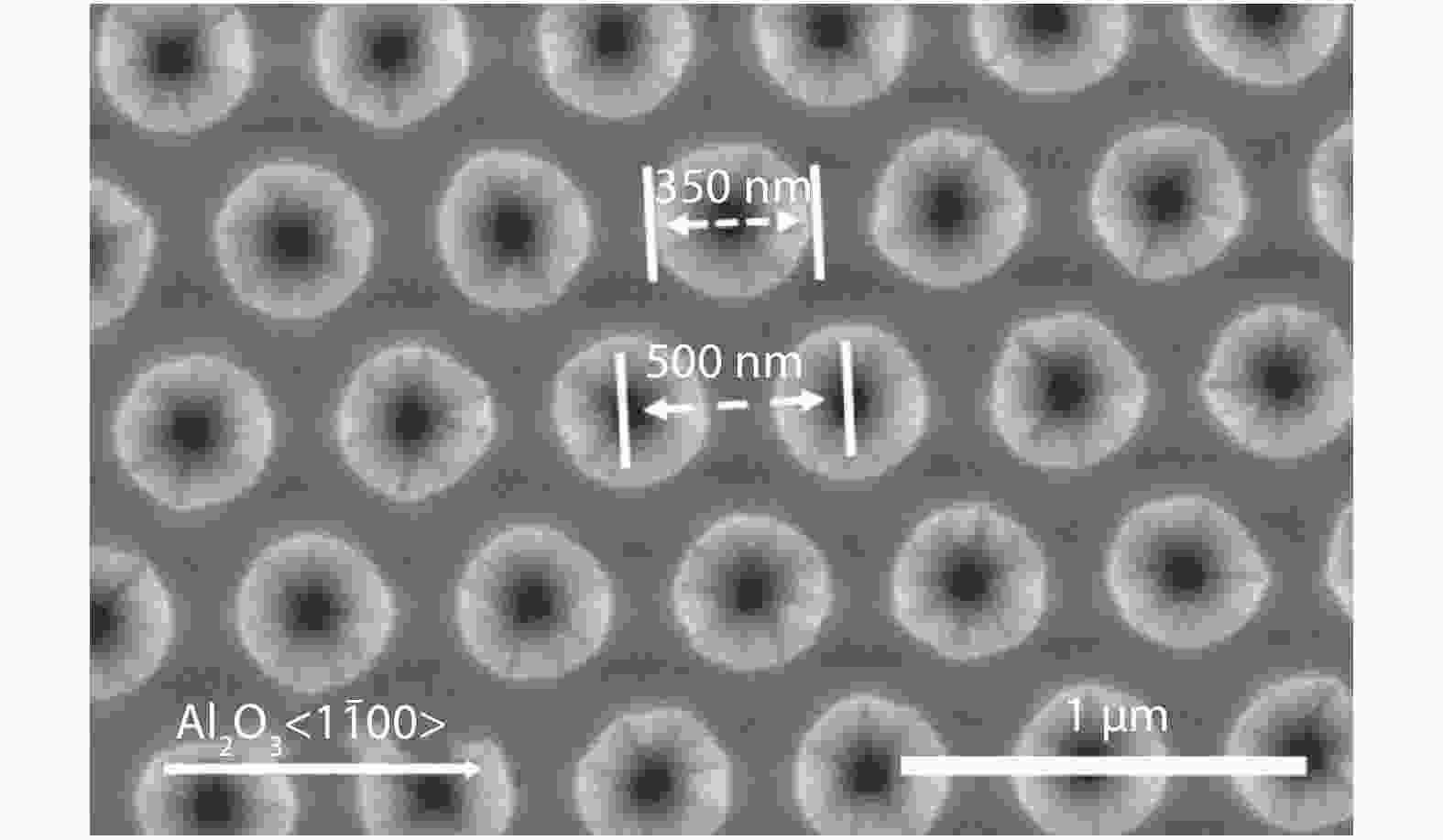
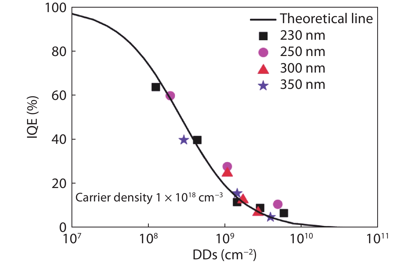
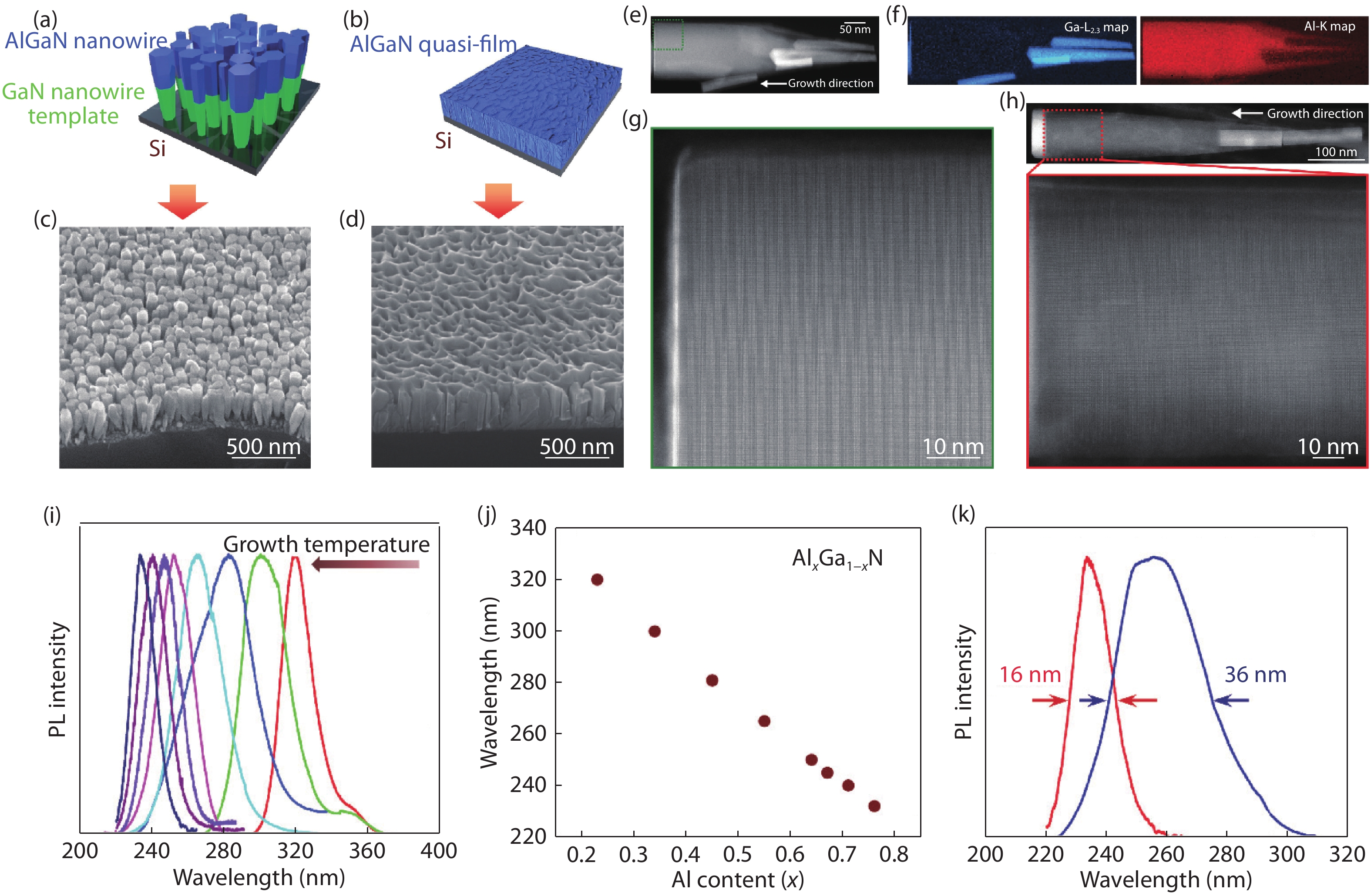
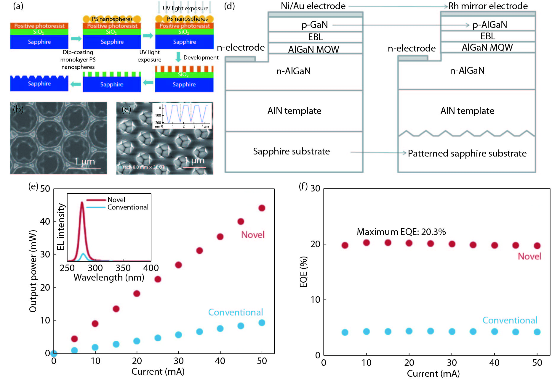
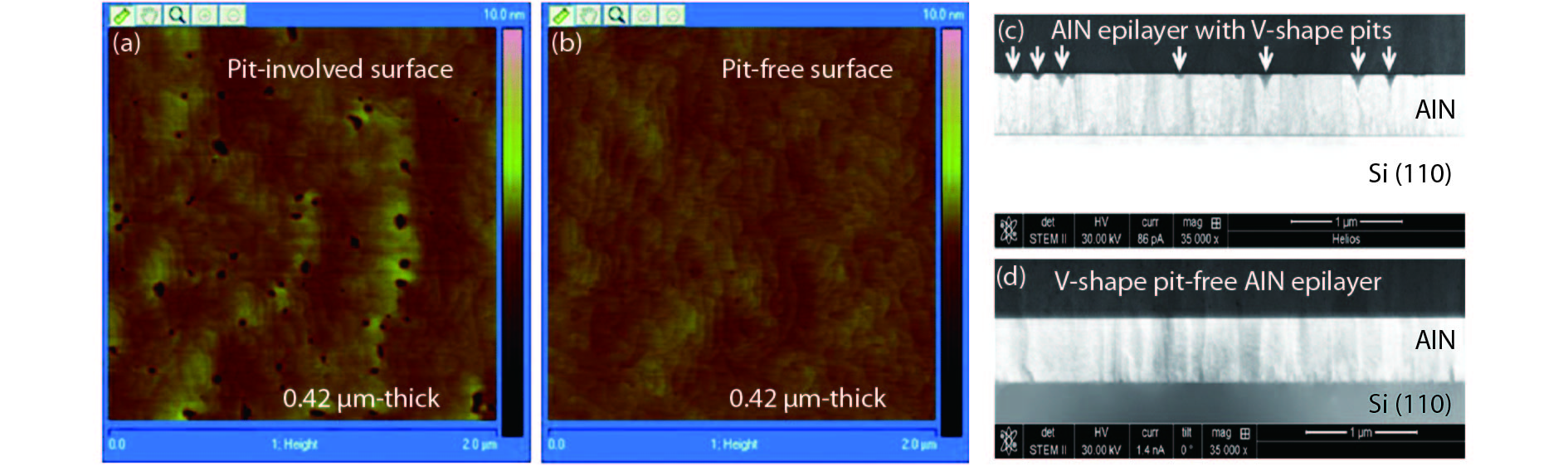
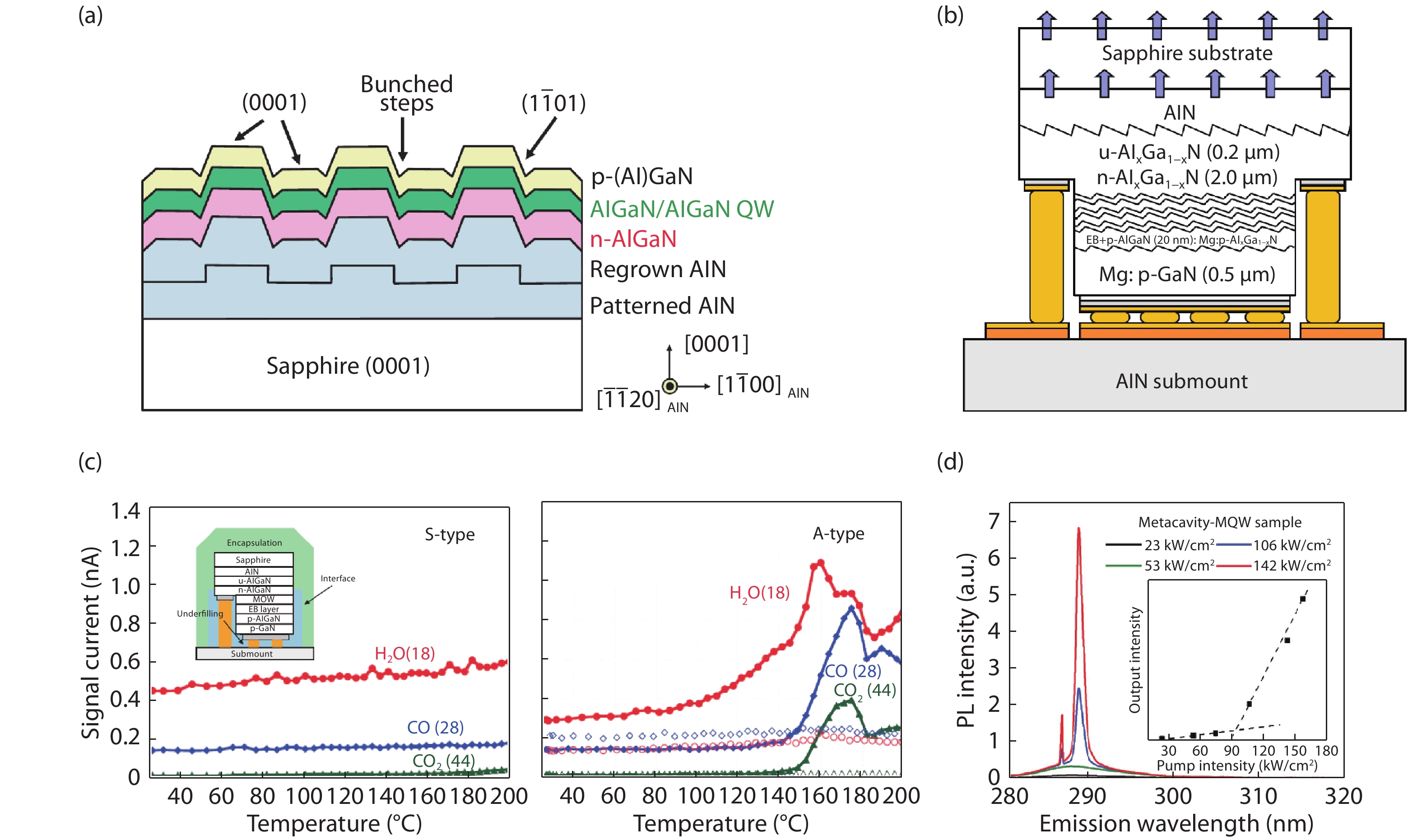
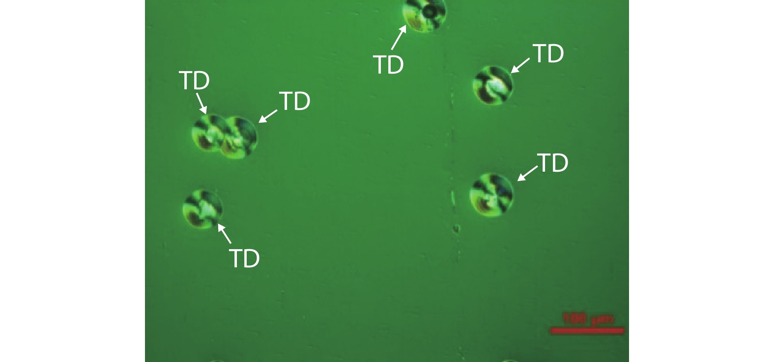
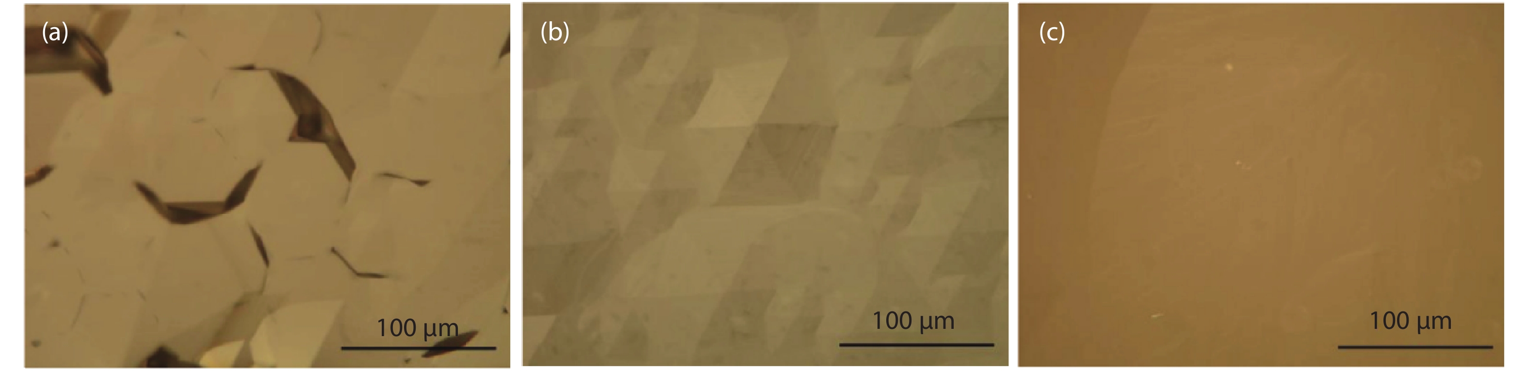
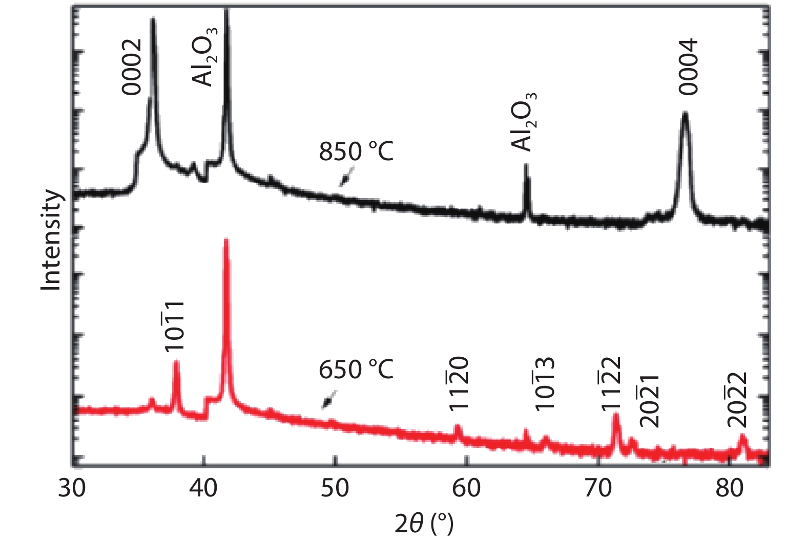
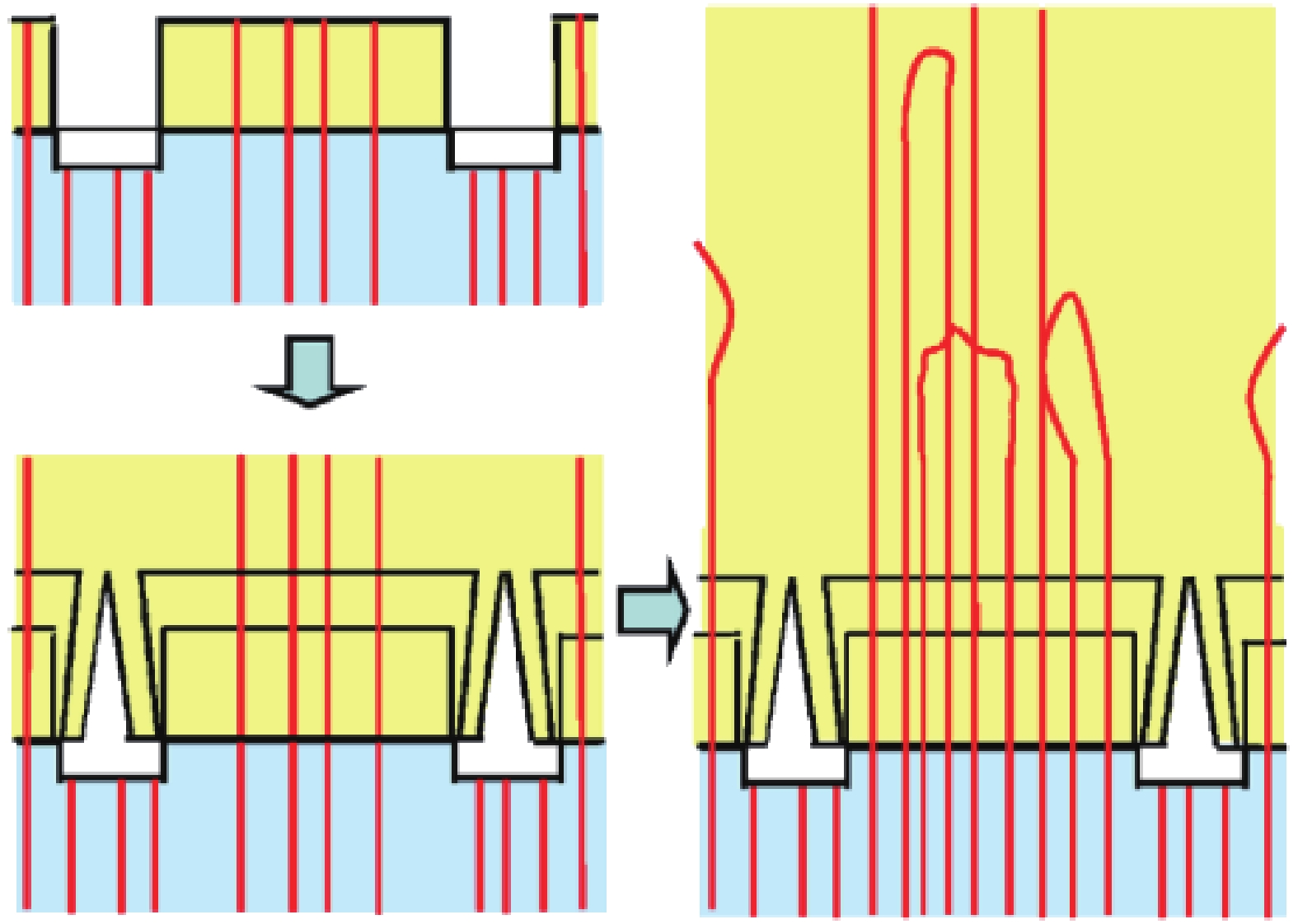
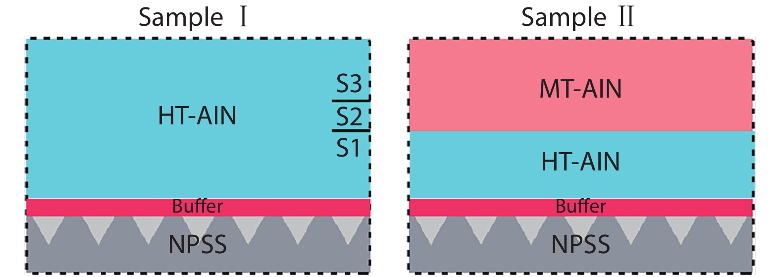
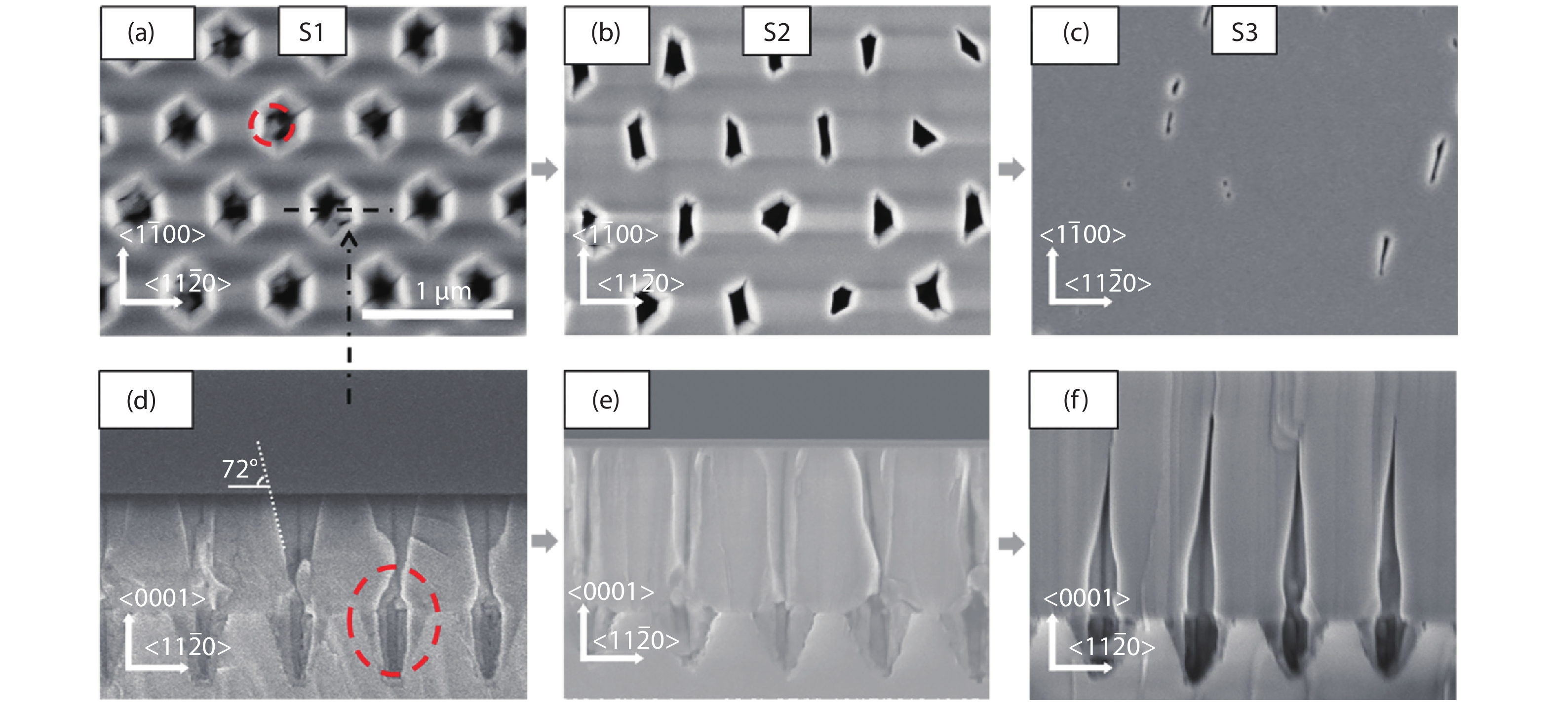
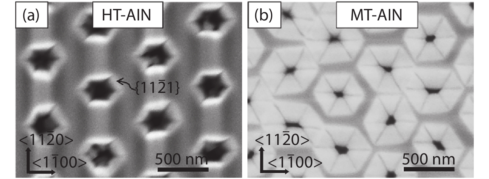
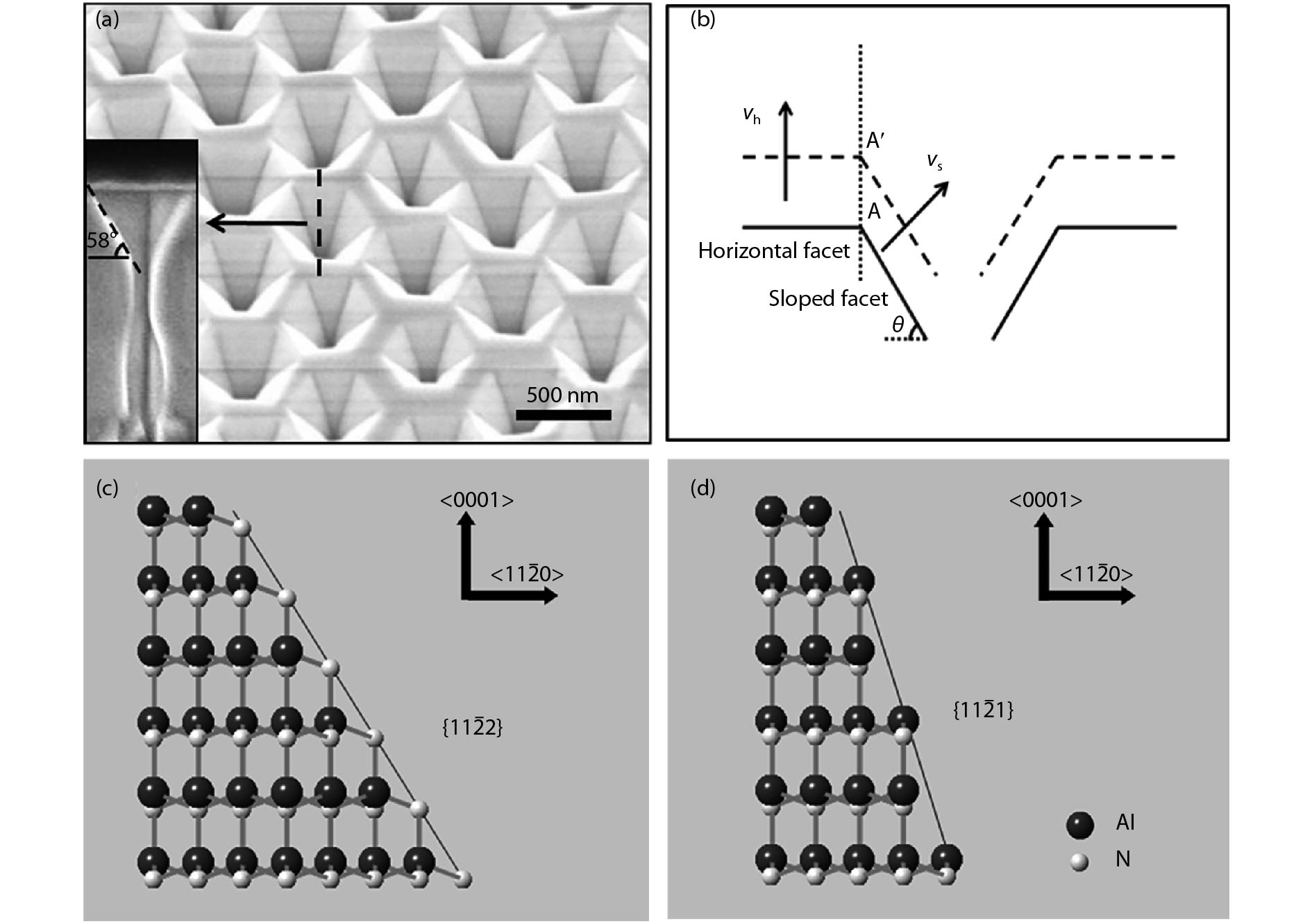
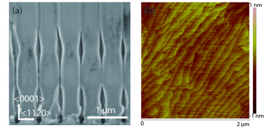
This study focused on the evolution of growth front about AlN growth on nano-patterned sapphire substrate by metal-organic chemical vapor deposition. The substrate with concave cones was fabricated by nano-imprint lithography and wet etching. Two samples with different epitaxy procedures were fabricated, manifesting as two-dimensional growth mode and three-dimensional growth mode, respectively. The results showed that growth temperature deeply influenced the growth modes and thus played a critical role in the coalescence of AlN. At a relatively high temperature, the AlN epilayer was progressively coalescence and the growth mode was two-dimensional. In this case, we found that the inclined semi-polar facets arising in the process of coalescence were


J. Semicond.
2019, 40(12): 122101 doi: 10.1088/1674-4926/40/12/122101
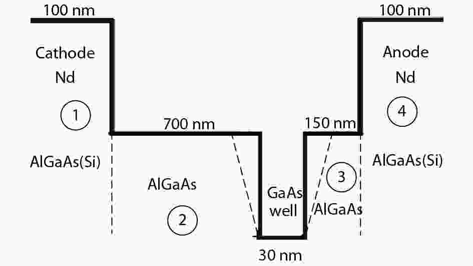
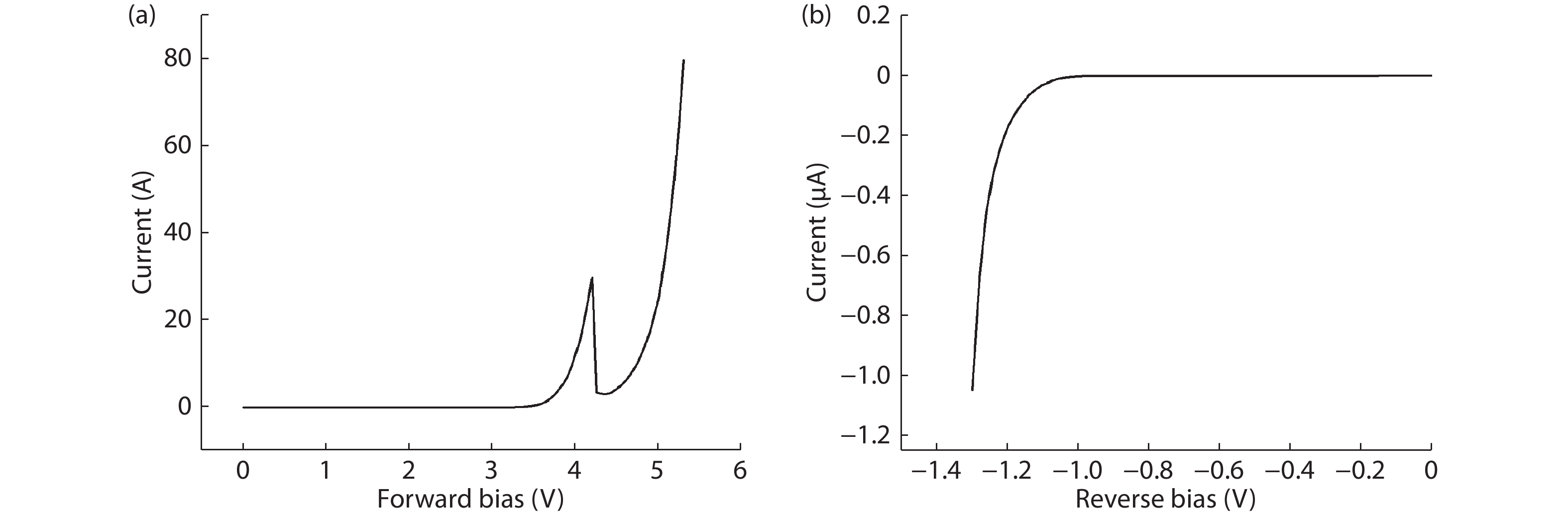
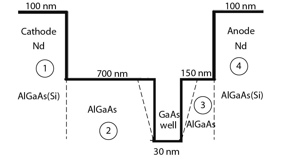
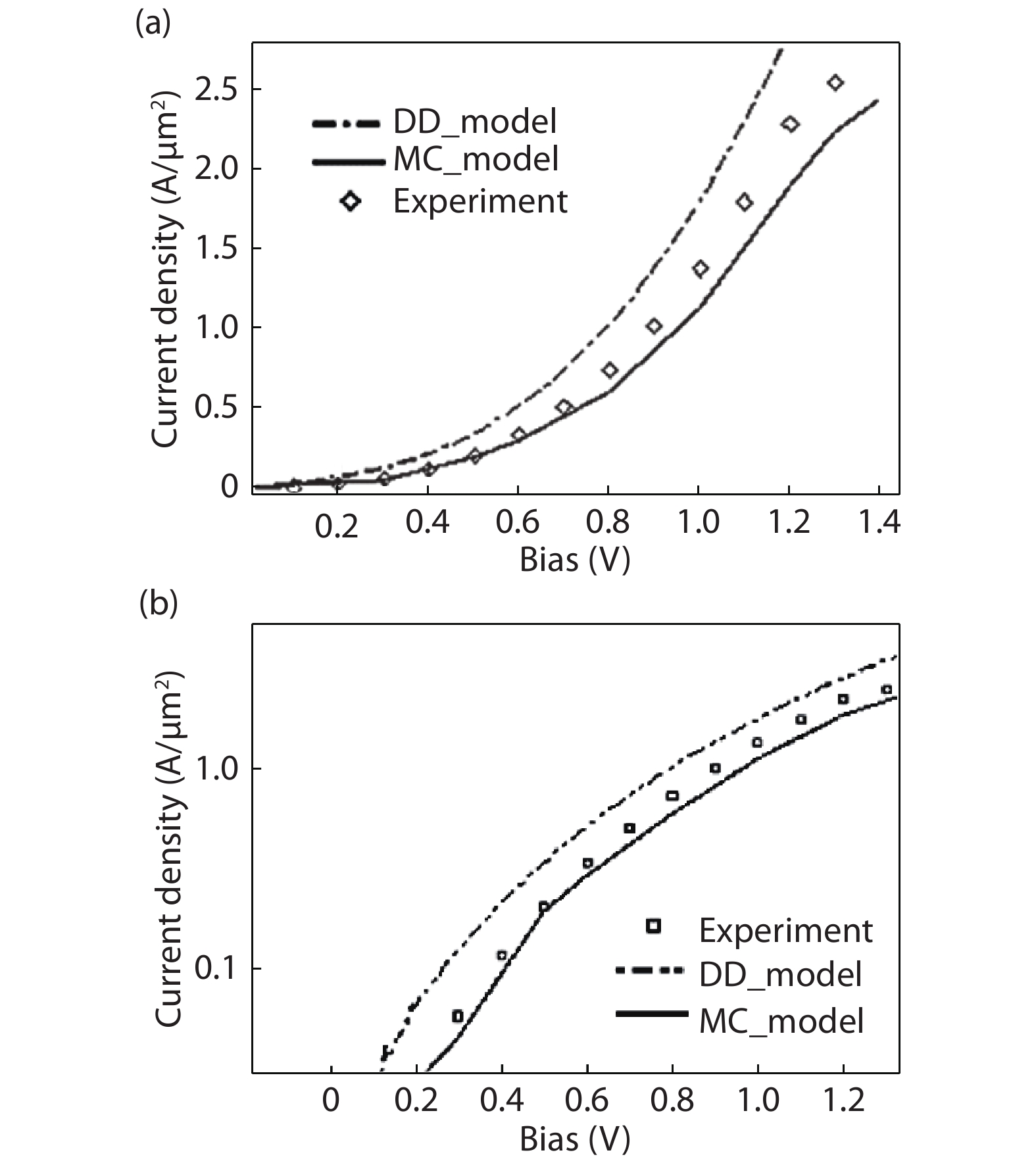
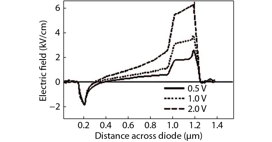
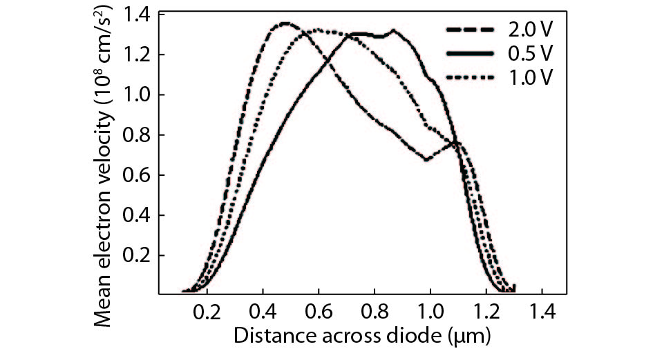
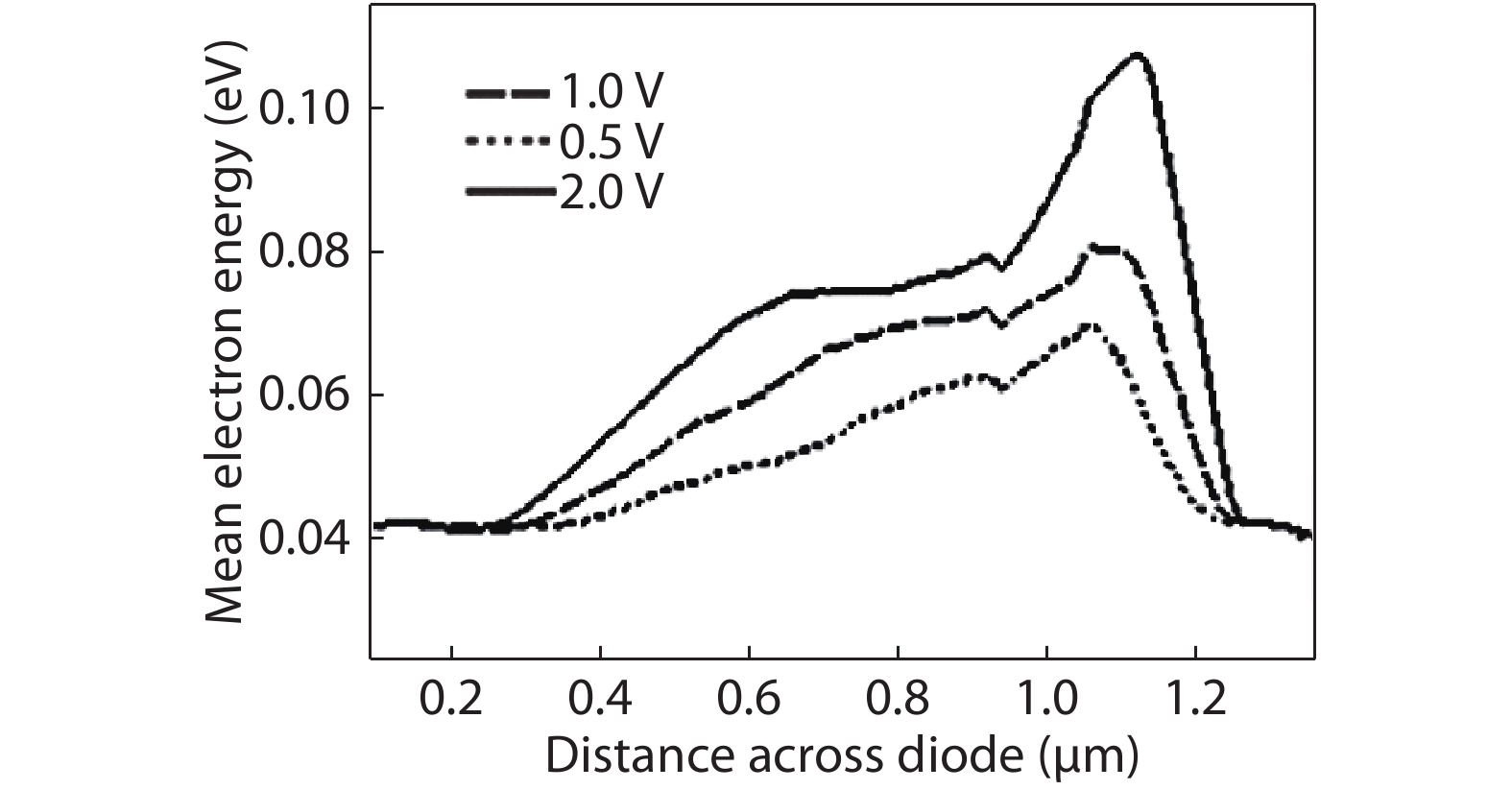
A study has just been carried out on hot electron effects in GaAs/Al0.3Ga0.7As potential well barrier (PWB) diodes using both Monte Carlo (MC) and drift-diffusion (DD) models of charge transport. We show the operation and behaviour of the diode in terms of electric field, mean electron velocity and potential, mean energy of electrons and Γ-valley population. The MC model predicts lower currents flowing through the diode due to back scattering at anode (collector) and carrier heating at higher bias. At a bias of 1.0 V, the current density obtained from experimental result, MC and DD simulation models are 1.35, 1.12 and 1.77 μA/μm2 respectively. The reduction in current over conventional model, is compensated to a certain extent because less charge settles in the potential well and so the barrier is slightly reduced. The DD model results in higher currents under the same bias and conditions. However, at very low bias specifically, up to 0.3 V without any carrier heating effects, the DD and MC models look pretty similar as experimental results. The significant differences observed in the I–V characteristics of the DD and MC models at higher biases confirm the importance of energy transport when considering these devices.

J. Semicond.
2019, 40(12): 122201 doi: 10.1088/1674-4926/40/12/122201
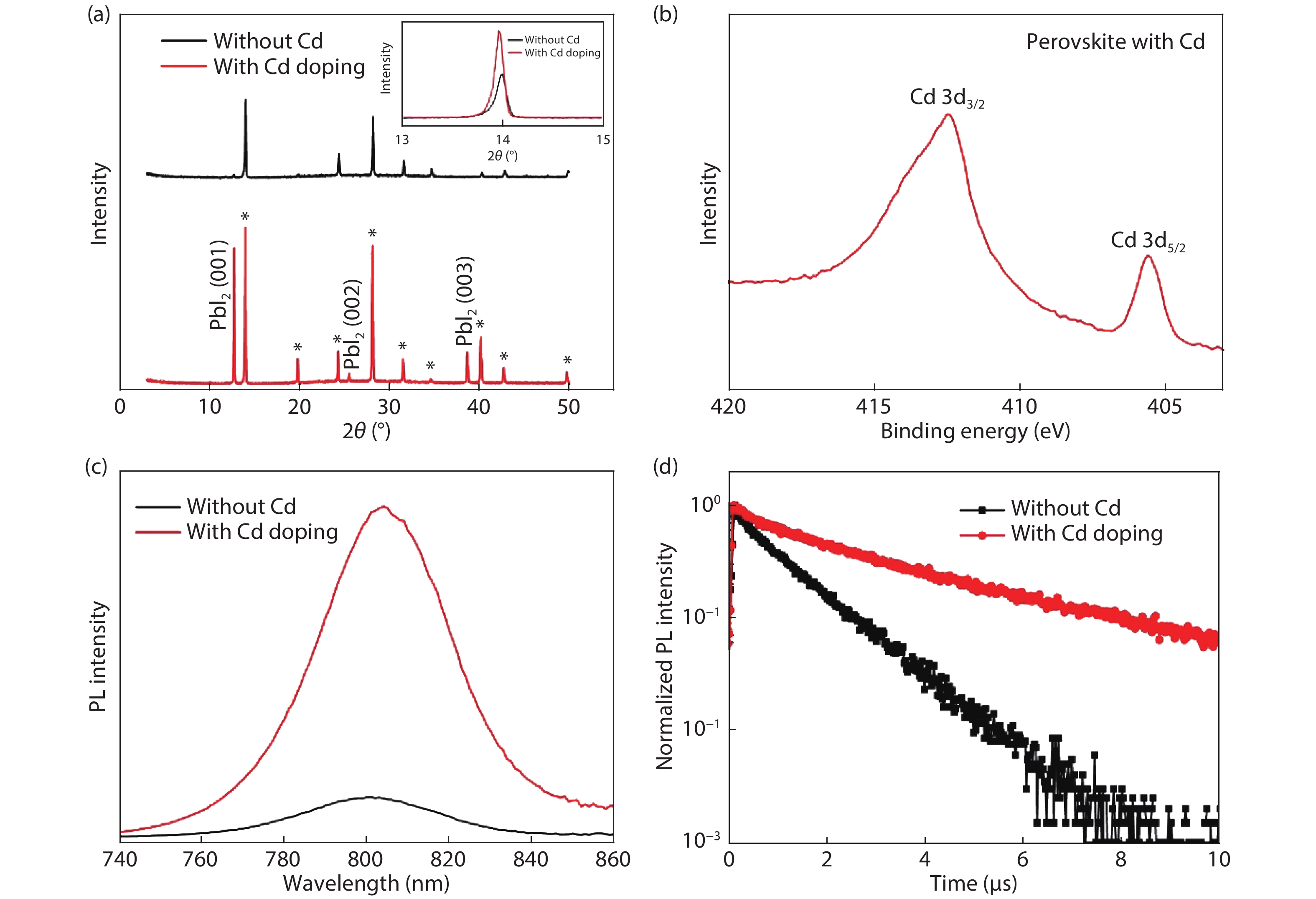
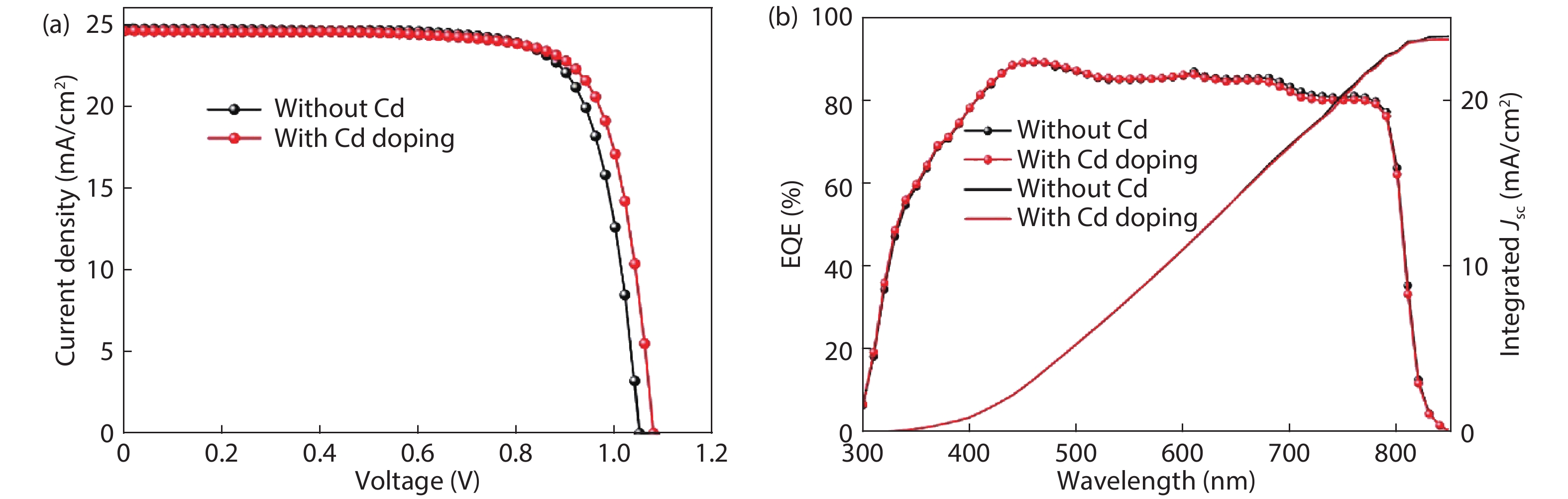
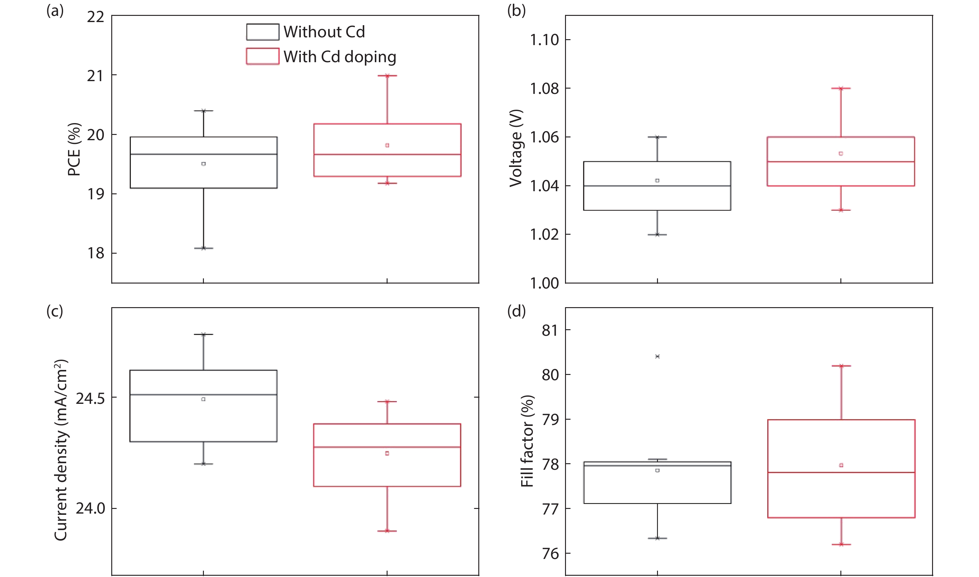
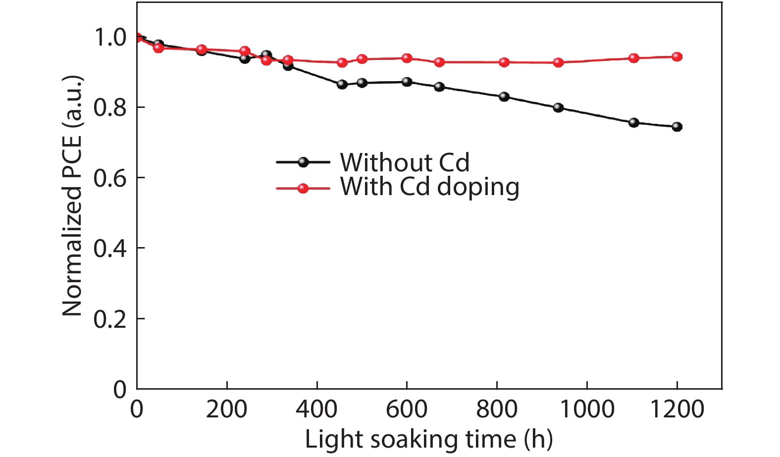
Although perovskite solar cells containing methylamine cation can show high power conversion efficiency, stability is a concern. Here, methylamine-free perovskite material CsxFA1–xPbI3 was synthesized by a one-step method. In addition, we incorporated smaller cadmium ions into mixed perovskite lattice to partially replace Pb ions to address the excessive internal strain in perovskite structure. We have found that the introduction of Cd can improve the crystallinity and the charge carrier lifetime of perovskite films. Consequently, a power conversion efficiency as high as 20.59% was achieved. More importantly, the devices retained 94% of their initial efficiency under 1200 h of continuous illumination.

J. Semicond.
2019, 40(12): 122401 doi: 10.1088/1674-4926/40/12/122401
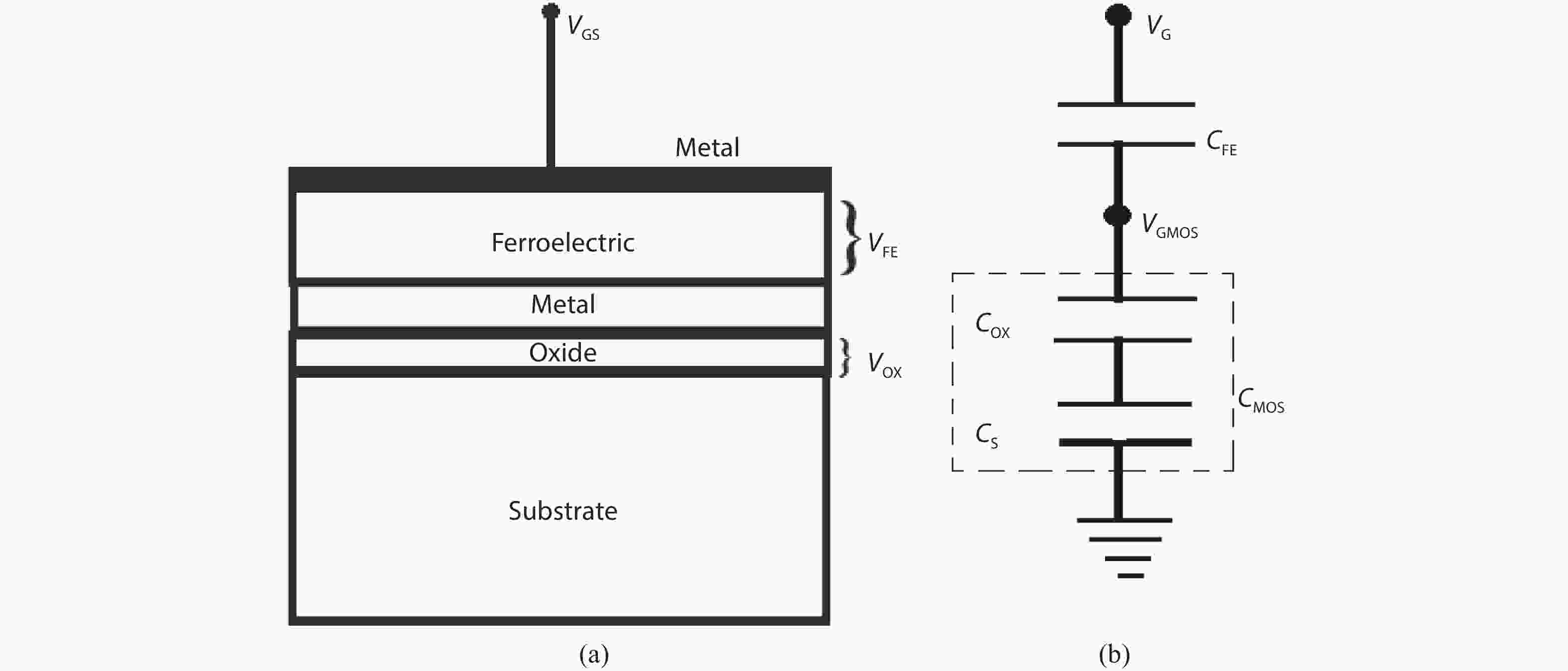
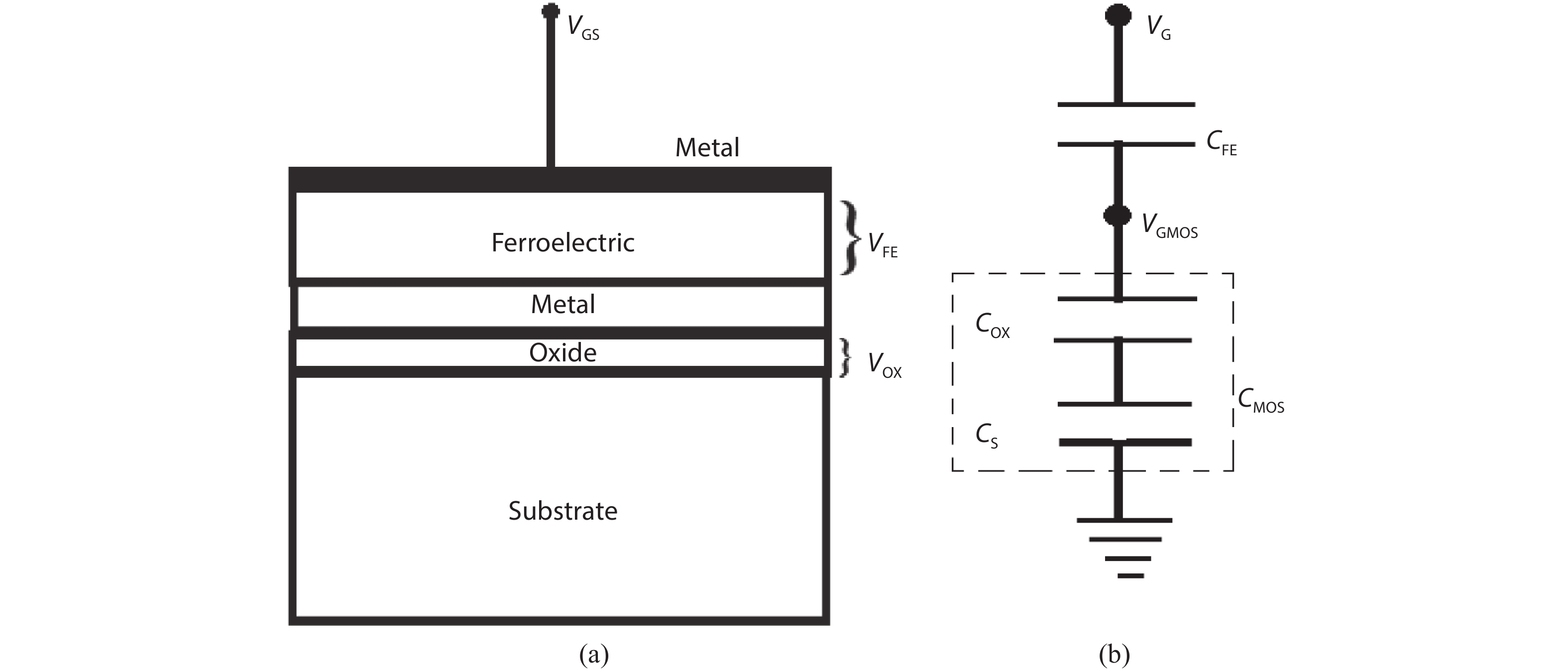
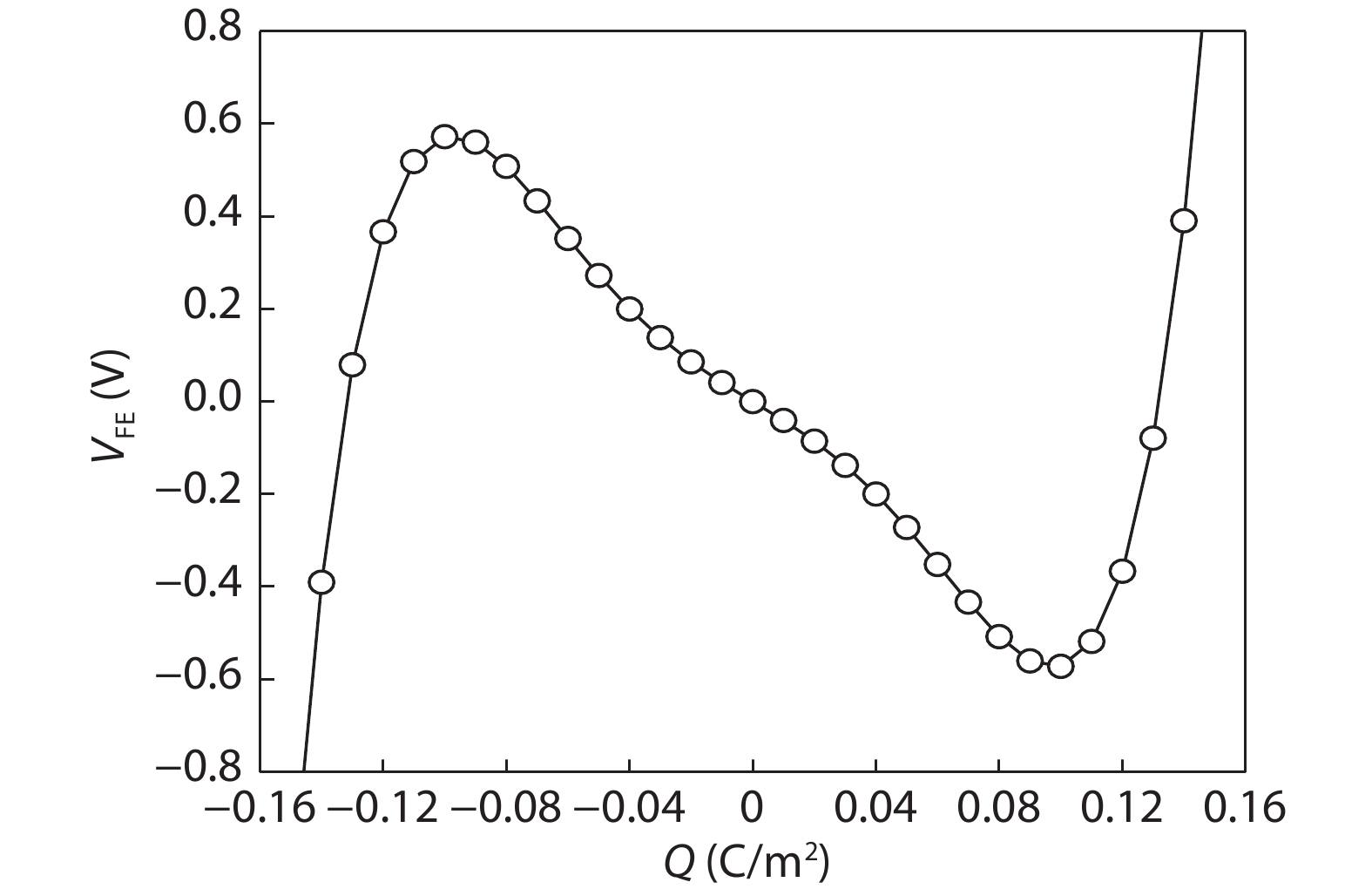
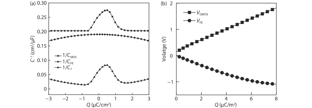
In this paper, we analytically study the relationship between the coercive field, remnant polarization and the thickness of a ferroelectric material, required for the minimum subthreshold swing in a negative capacitance capacitor. The interdependence of the ferroelectric material properties shown in this study is defined by the capacitance matching conditions in the subthreshold region in an NC capacitor. In this paper, we propose an analytical model to find the optimal ferroelectric thickness and channel doping to achieve a minimum subthreshold swing, due to a particular ferroelectric material. Our results have been validated against the numerical and experimental results already available in the literature. Furthermore, we obtain the minimum possible subthreshold swing for different ferroelectric materials used in the gate stack of an NC-FET in the context of a manufacturable semiconductor technology. Our results are presented in the form of a table, which shows the calculated channel doping, ferroelectric thickness and minimum subthreshold for five different ferroelectric materials.
J. Semicond.
2019, 40(12): 122402 doi: 10.1088/1674-4926/40/12/122402

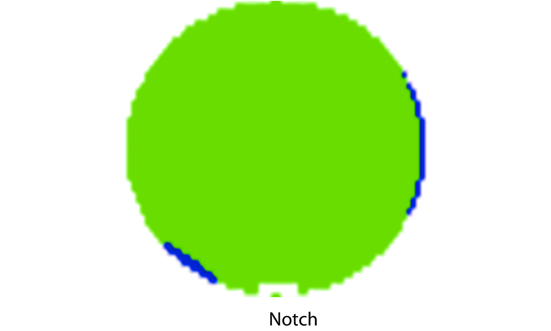
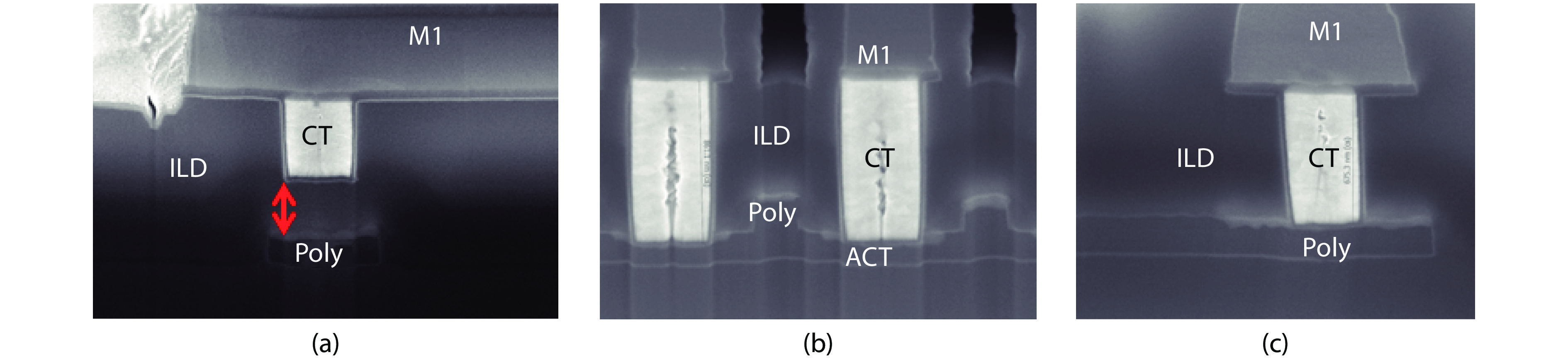
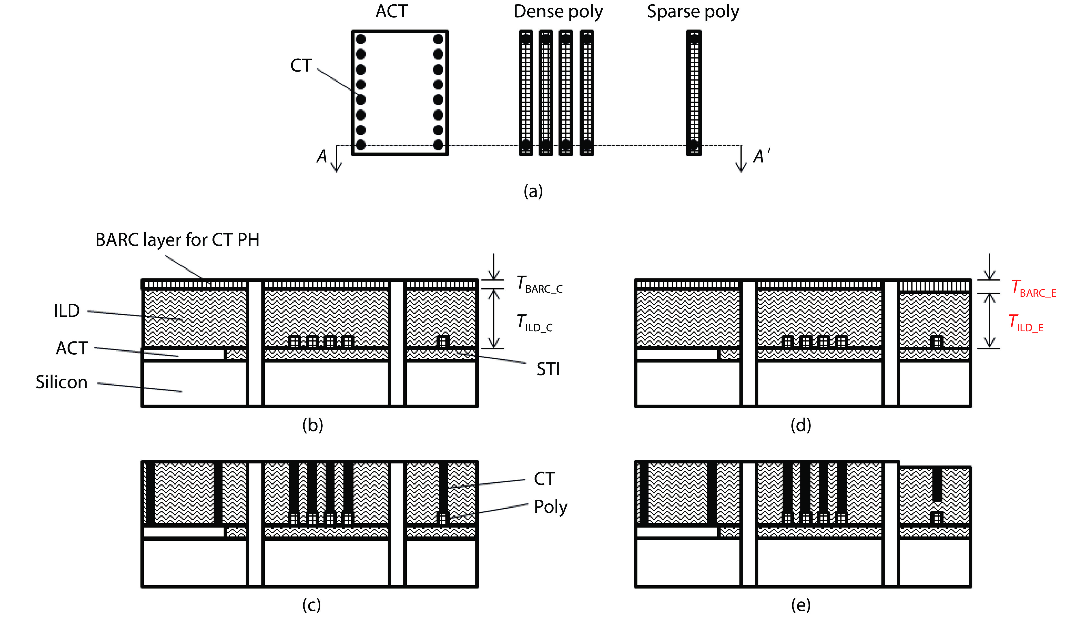
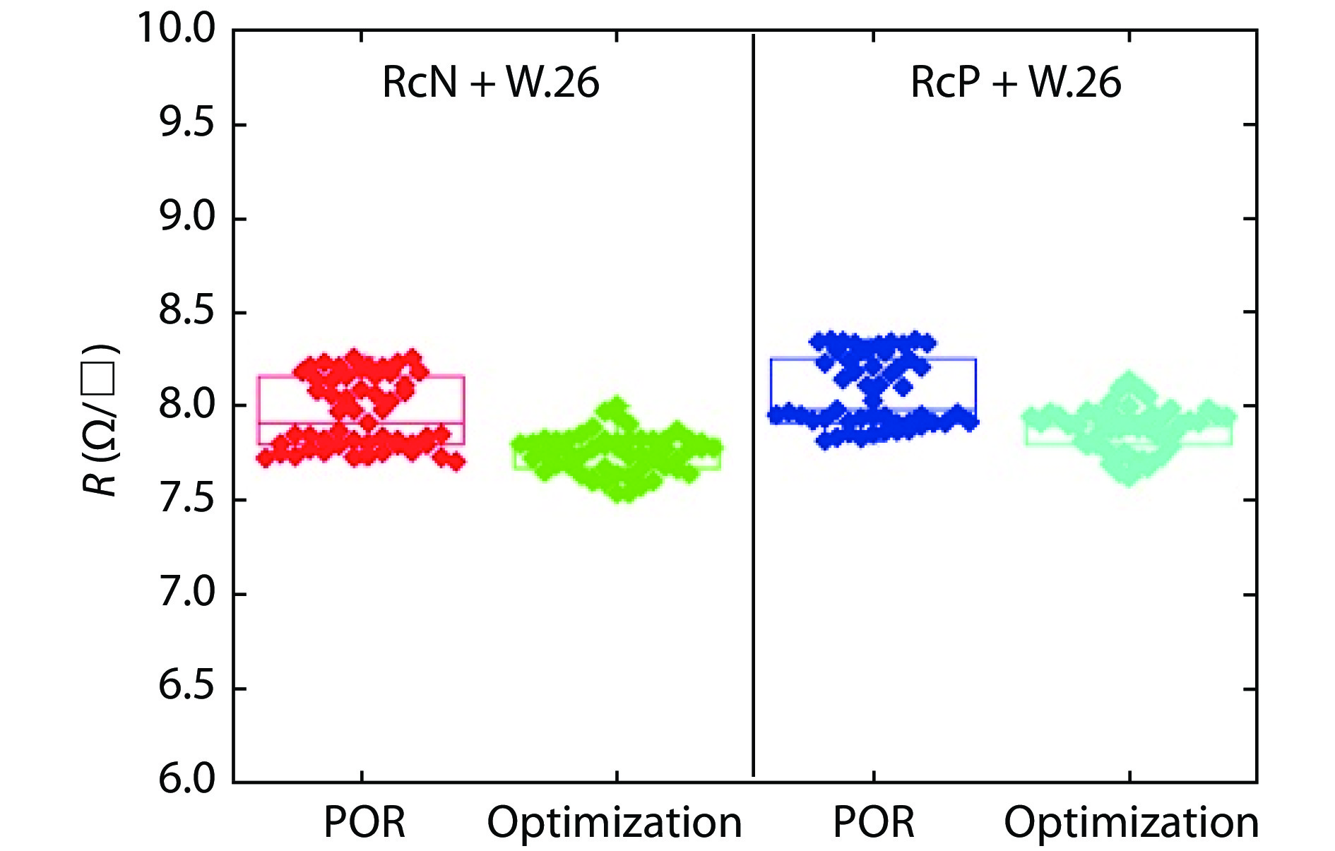
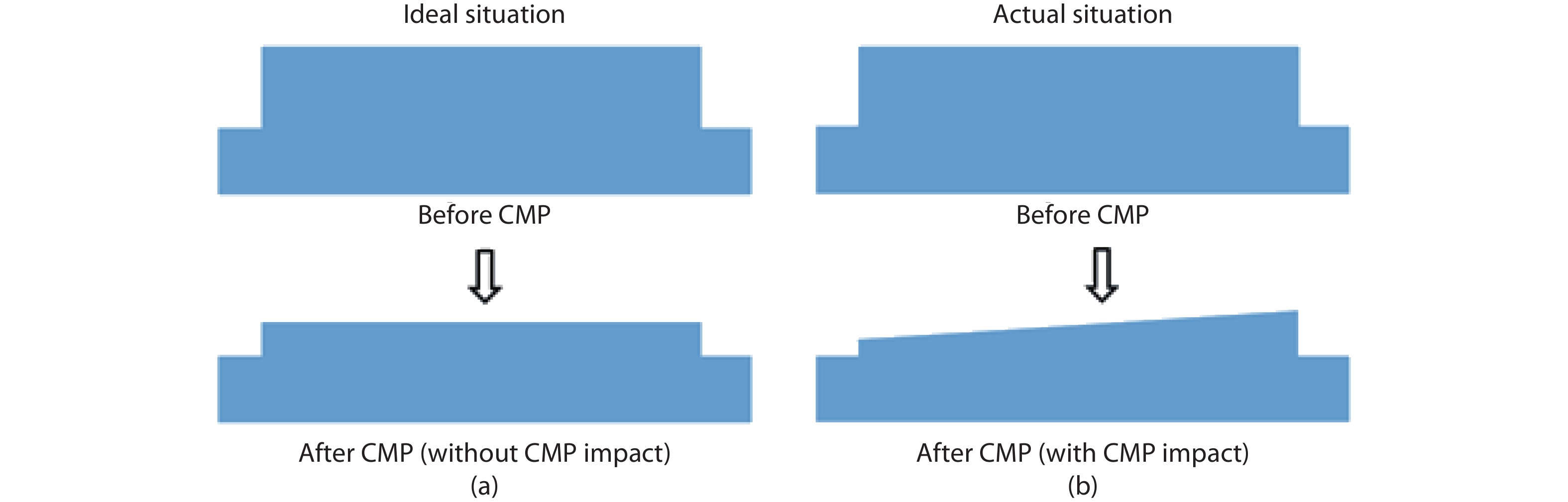
Radio-frequency (RF) process products suffer from a wafer edge low yield issue, which is induced by contact opening. A failure mechanism has been proposed that is based on the characteristics of a wafer edge film stack. The large step height at the wafer’s edge leads to worse planarization for the sparse poly-pattern region during the inter-layer dielectric (ILD) chemical mechanical polishing (CMP) process. A thicker bottom anti-reflect coating (BARC) layer was introduced for a sparse poly-pattern at the wafer edge region. The contact open issue was solved by increasing the break through (BT) time to get a large enough window. Well profile and resistance uniformity were obtained by contact etch recipe optimization.


J. Semicond.
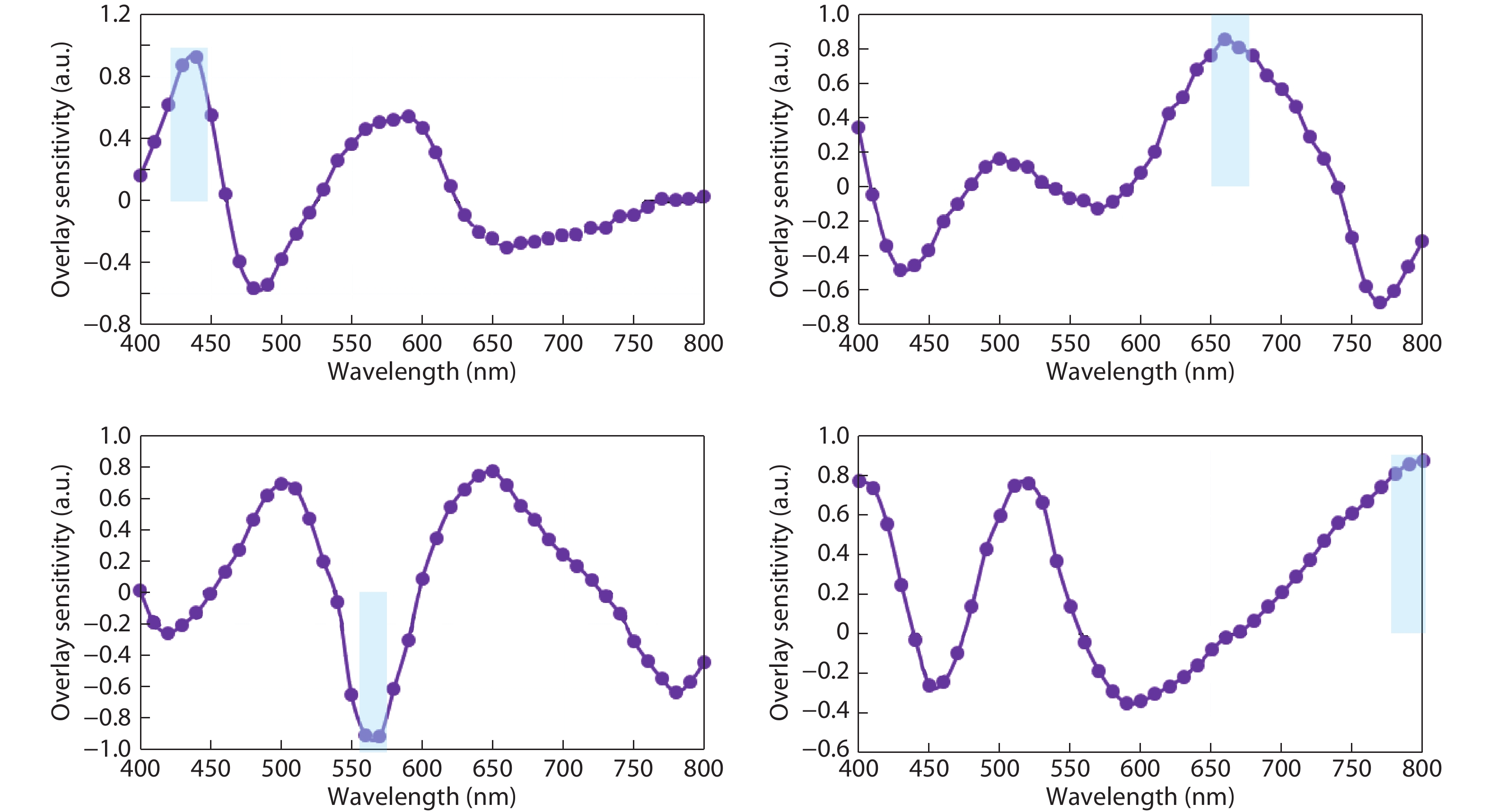
2019, 40(12): 122403 doi: 10.1088/1674-4926/40/12/122403

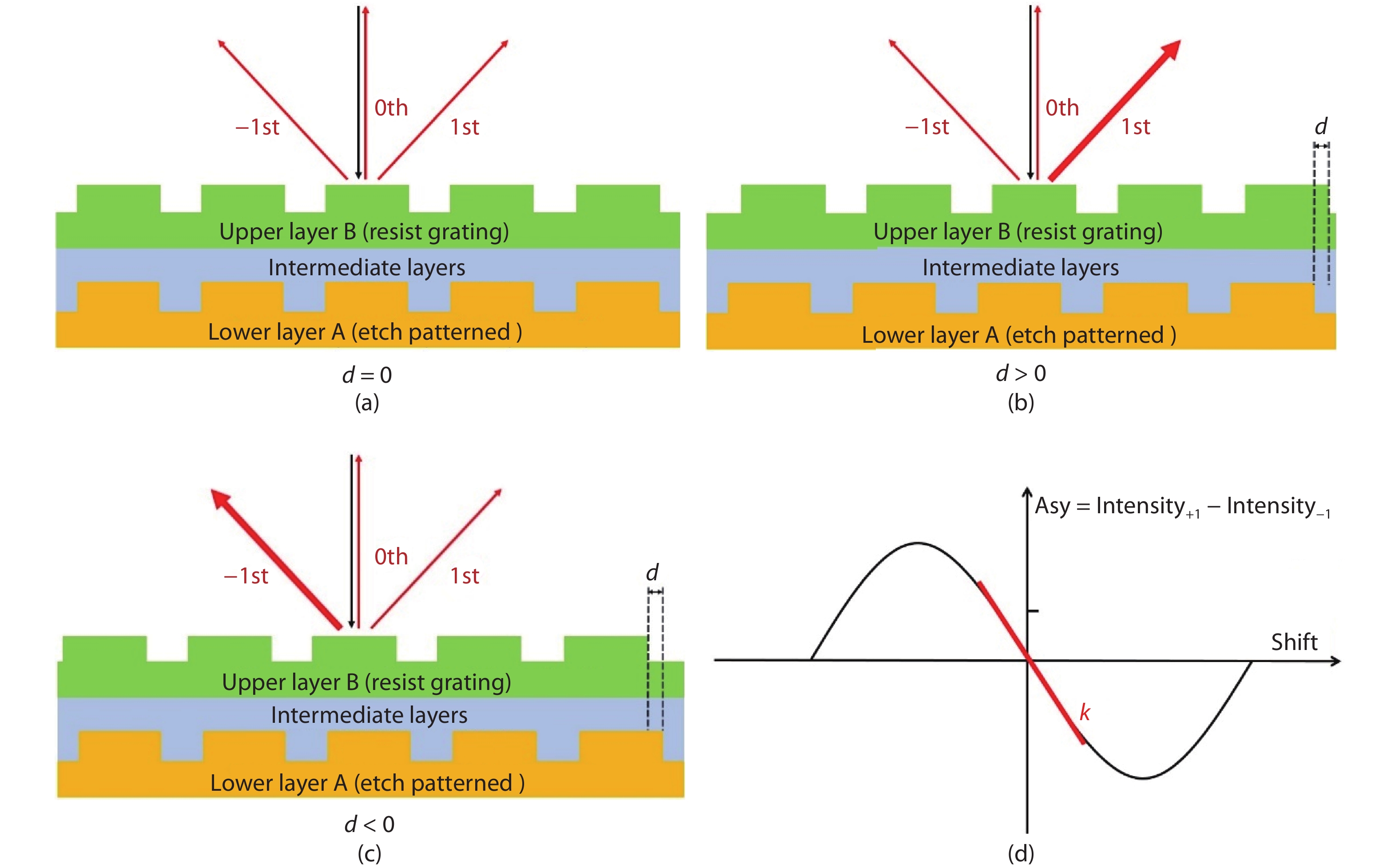
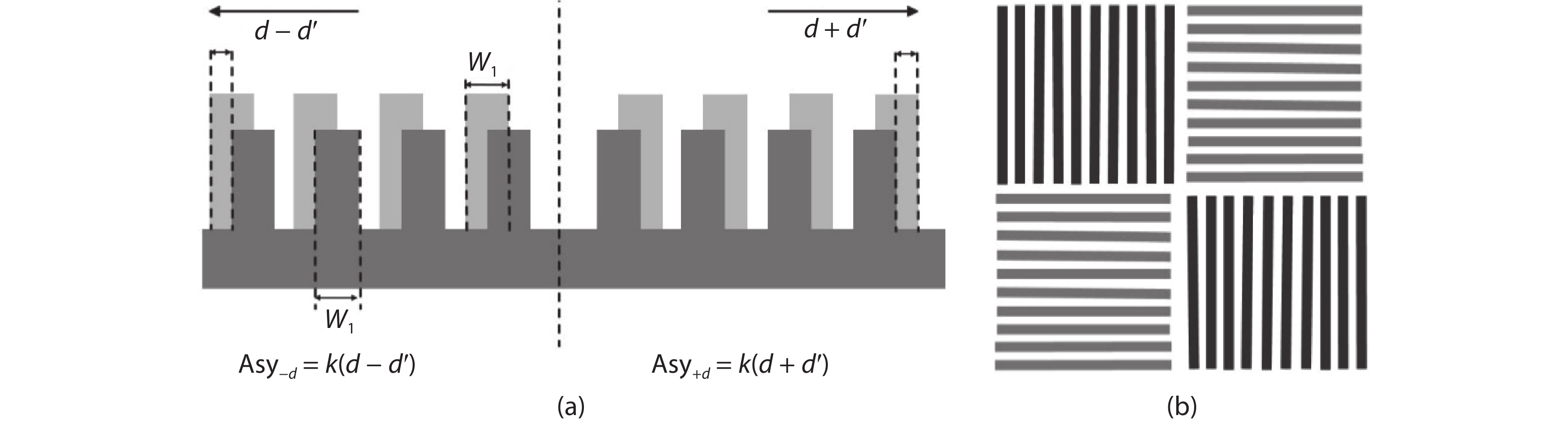
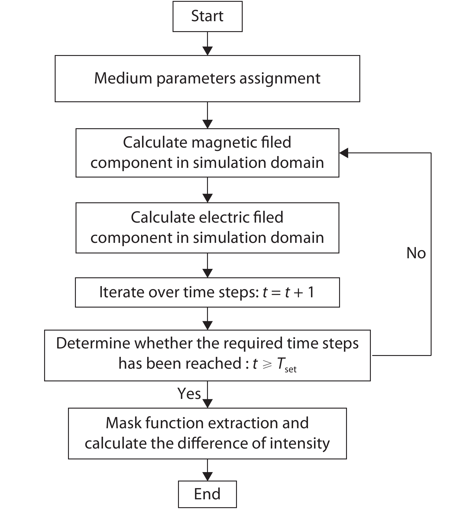
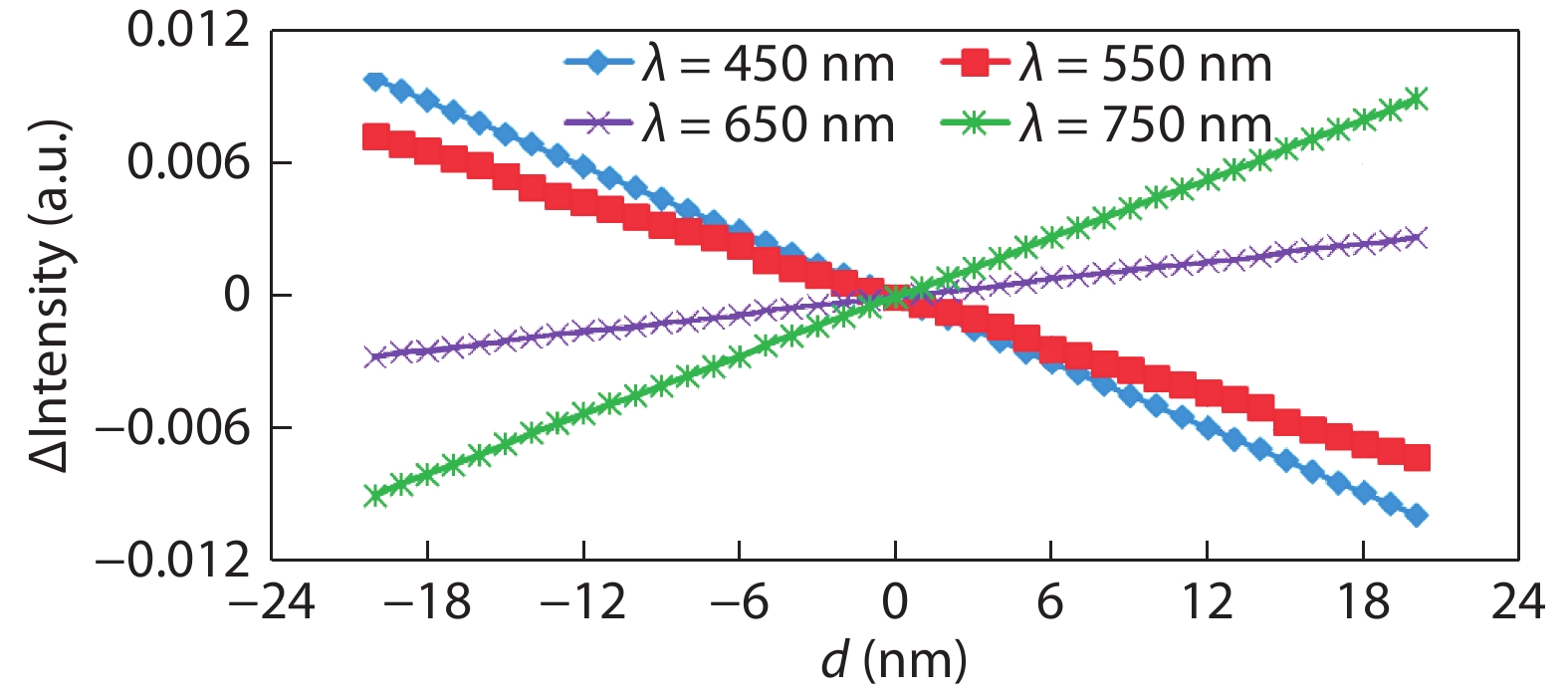
A physical model for simulating overlay metrology employing diffraction based overlay (DBO) principles is built. It can help to optimize the metrology wavelength selection in DBO. Simulation result of DBO metrology with a model based on the finite-difference time-domain (FDTD) method is presented. A common case (bottom mark asymmetry) in which error signals are always induced in DBO measurement due to the process imperfection were discussed. The overlay sensitivity of the DBO measurement across the visible illumination spectrum has been performed and compared. After adjusting the model parameters compatible with the actual measurement conditions, the metrology wavelengths which provide the accuracy and robustness of DBO measurement can be optimized.


J. Semicond.
2019, 40(12): 122404 doi: 10.1088/1674-4926/40/12/122404
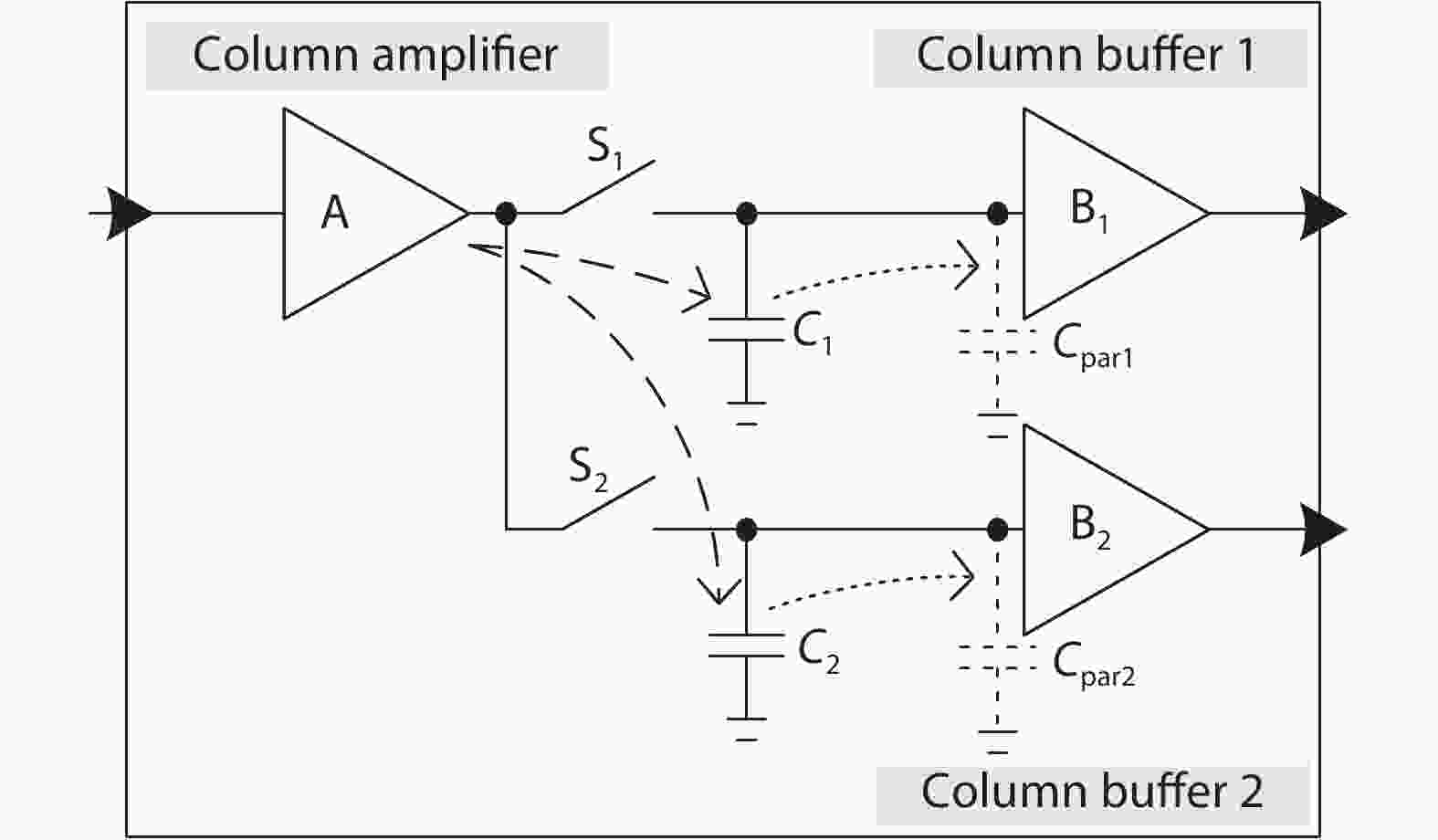
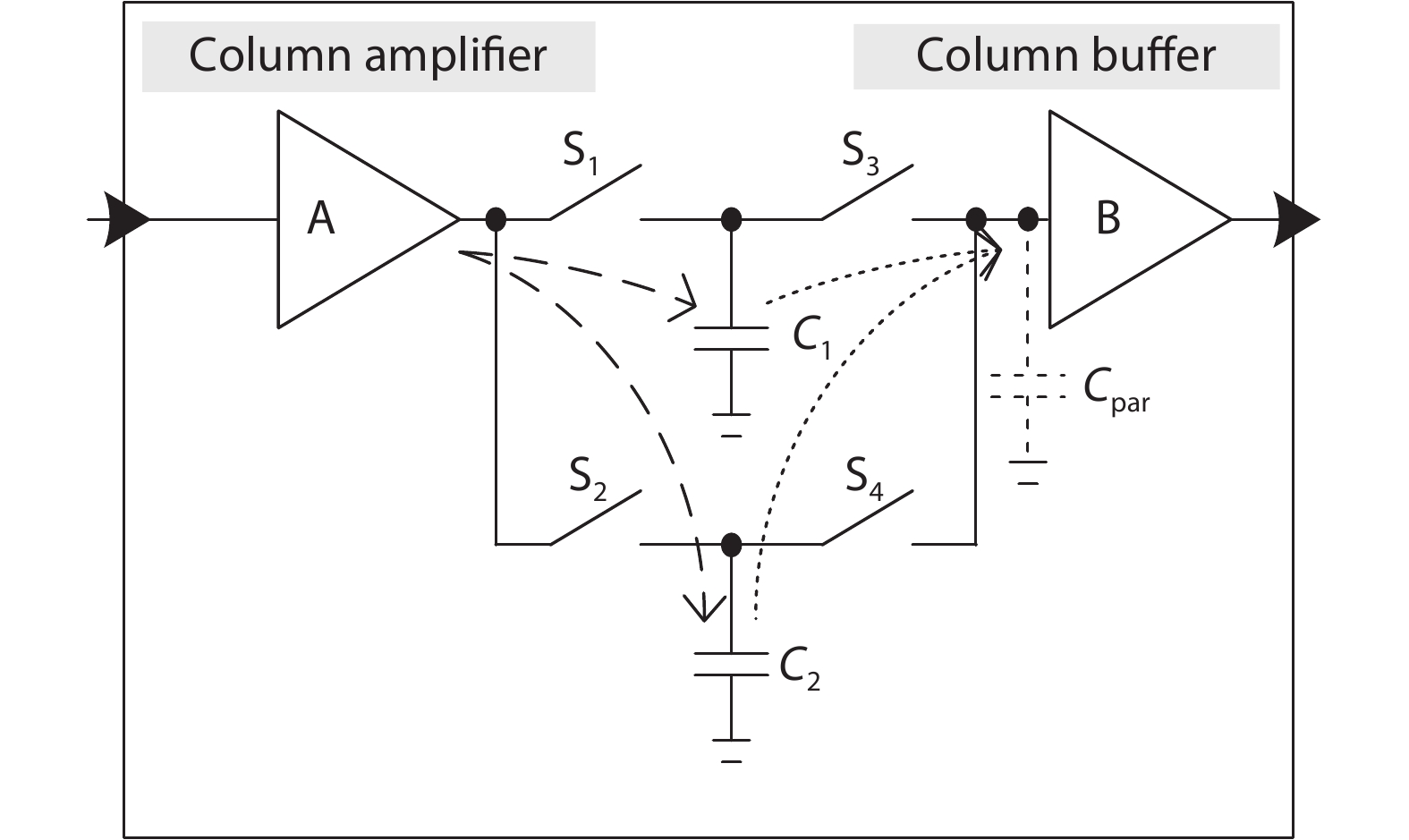
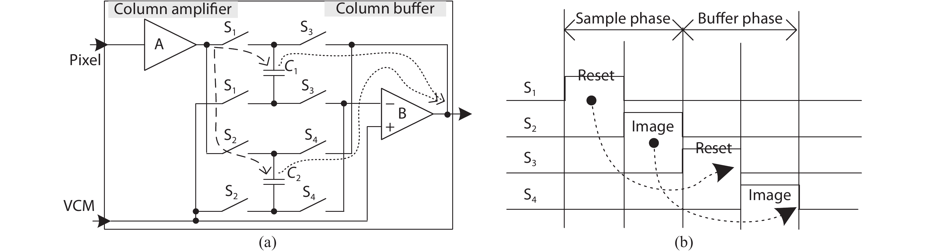
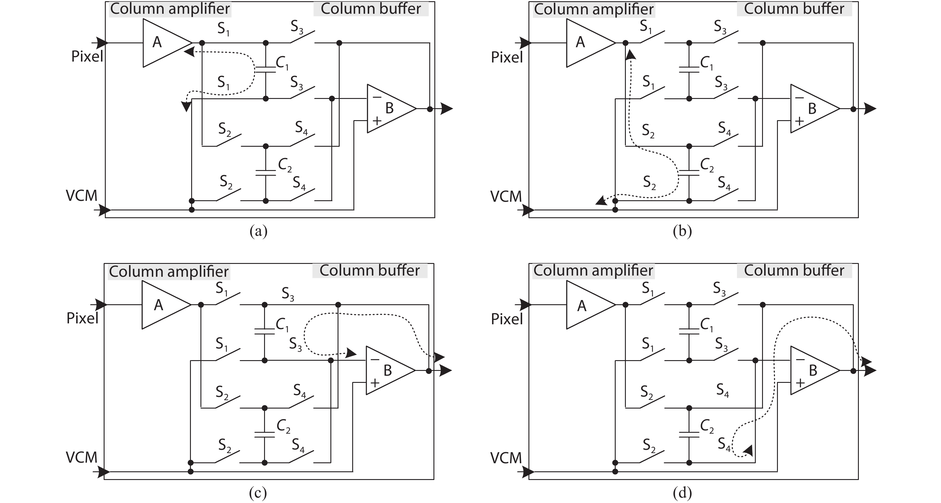
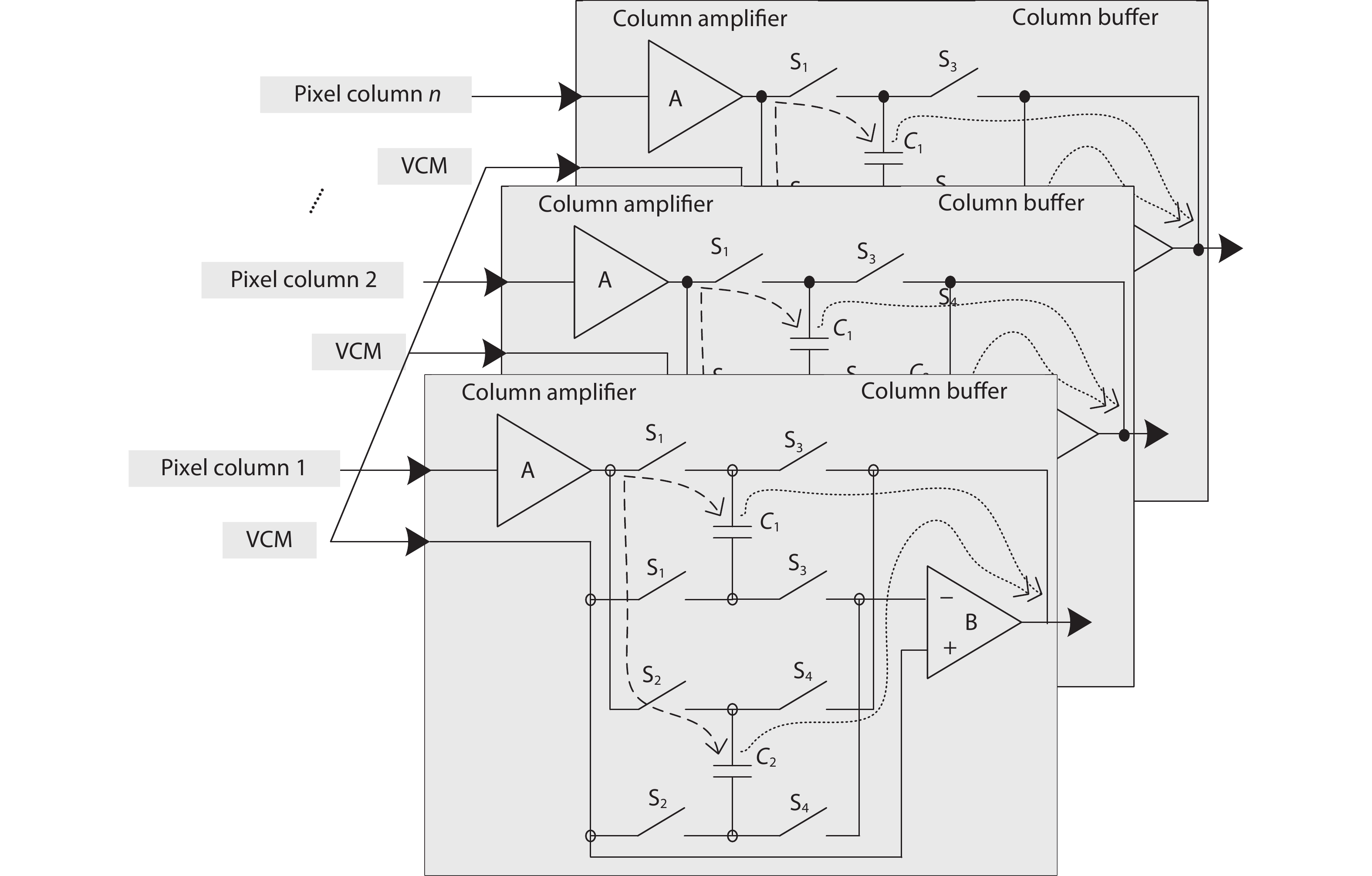
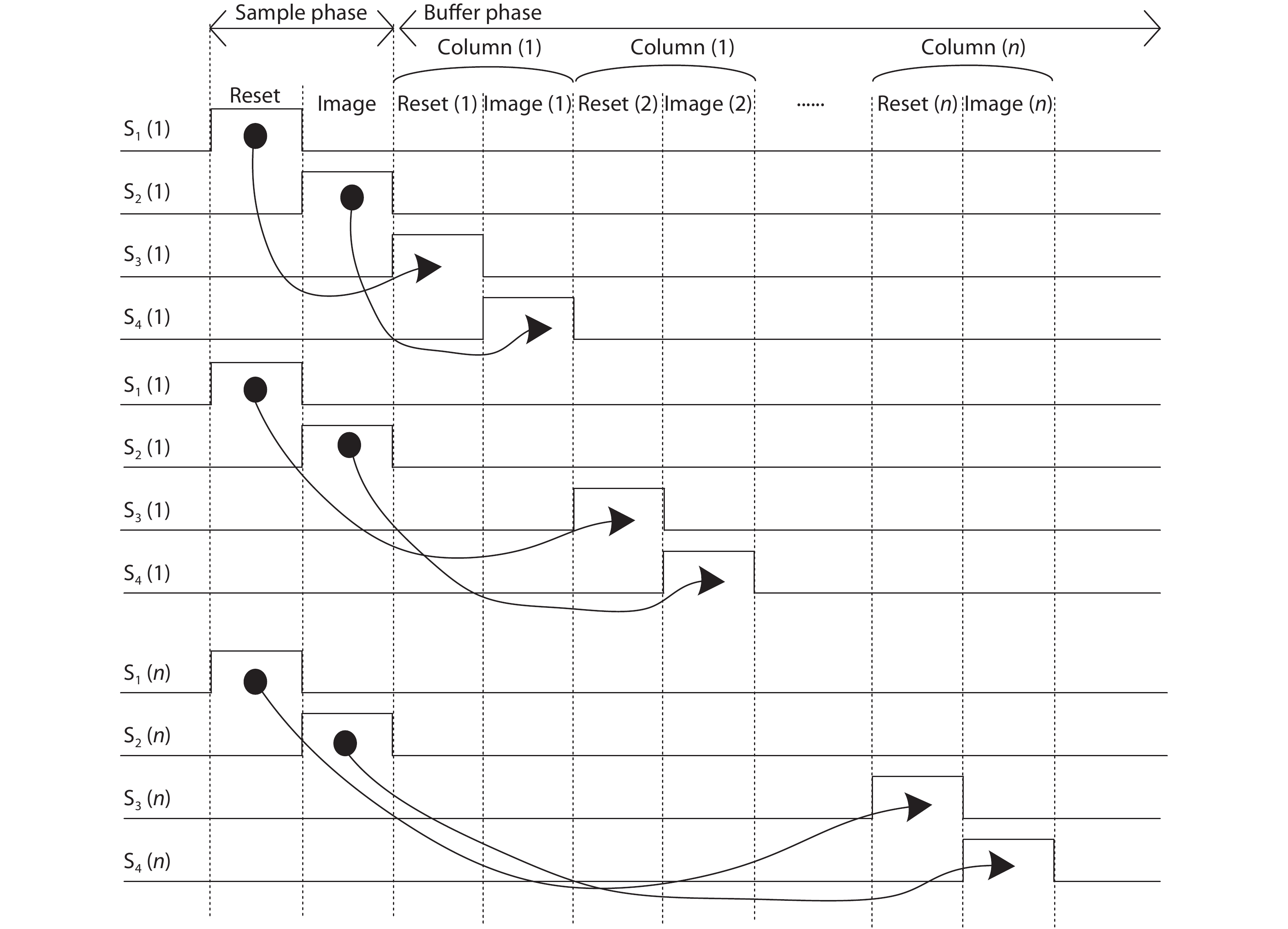
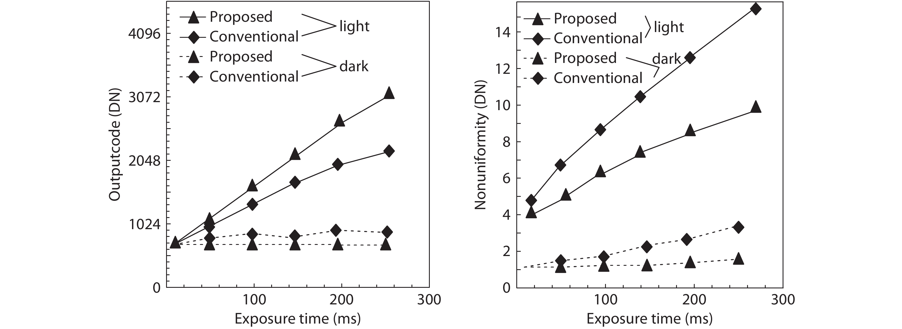
High linearity and low noise column readout chain are two key factors in CMOS image sensor. However, offset mismatch and charge sharing always exist in the conventional column wise readout implementation, even adopting the technology of correlated double sample. A simple column readout circuit with improved offset mismatch and charge sharing for CMOS image sensor is proposed in this paper. Based on the bottom plate sampling and fixed common level method, this novel design can avoid the offset nonuniformity between the two buffers. Also, the single buffer and switched capacitor technique can effectively suppress the charge sharing caused by the varied operating point. The proposed approach is experimentally verified in a 1024 × 1024 prototype chip designed and fabricated in 55 nm low power CMOS process. The measurement results show that the linear range is extended by 20%, the readout noise of bright and dark fields is reduced by 40% and 30% respectively, and the improved photo response nonuniformity is up to 1.16%. Finally, a raw sample image taken by the prototype sensor shows the excellent practical performance.


J. Semicond.
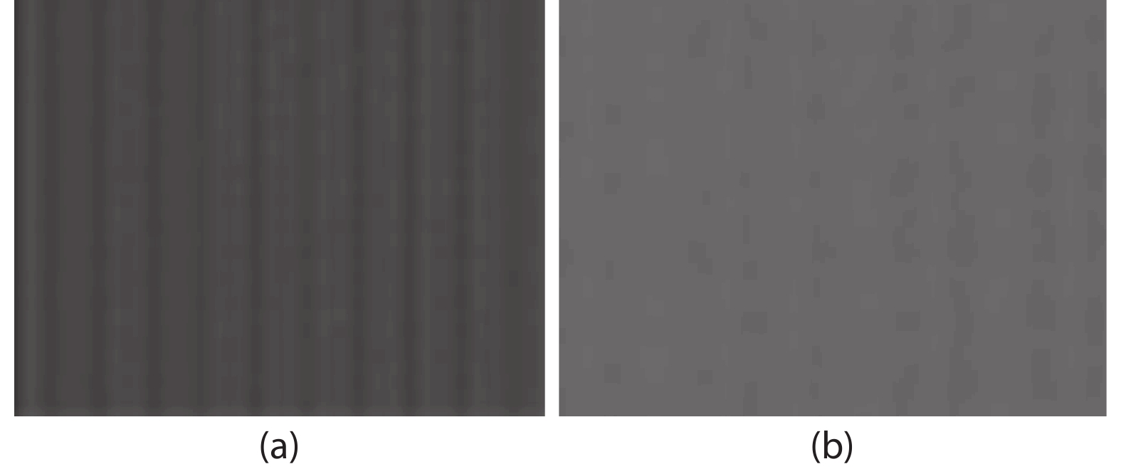
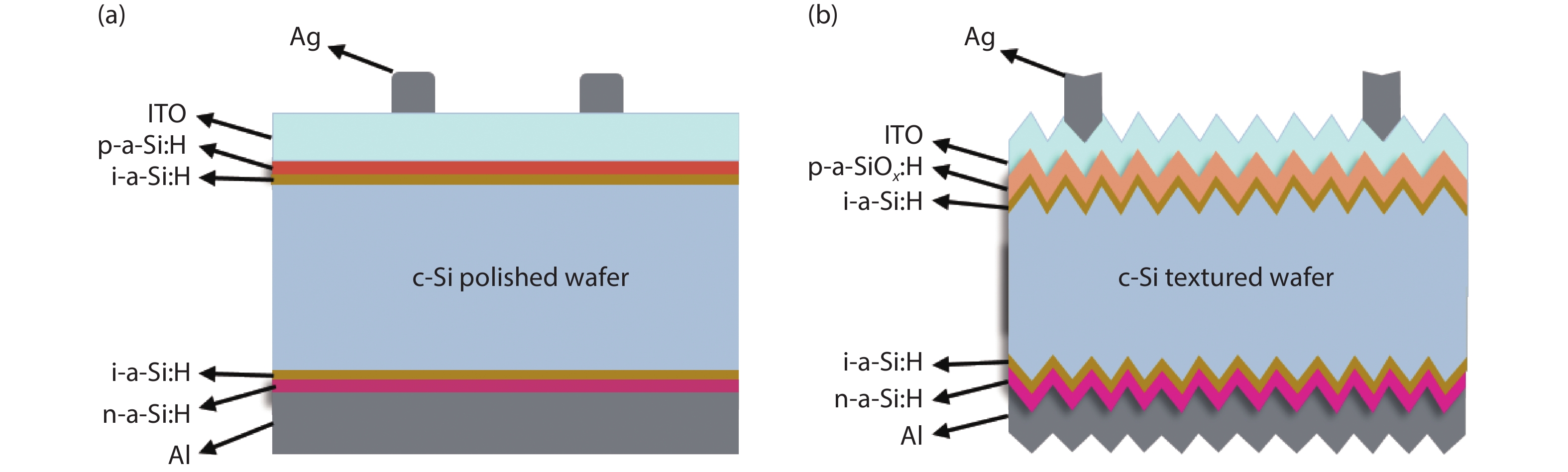
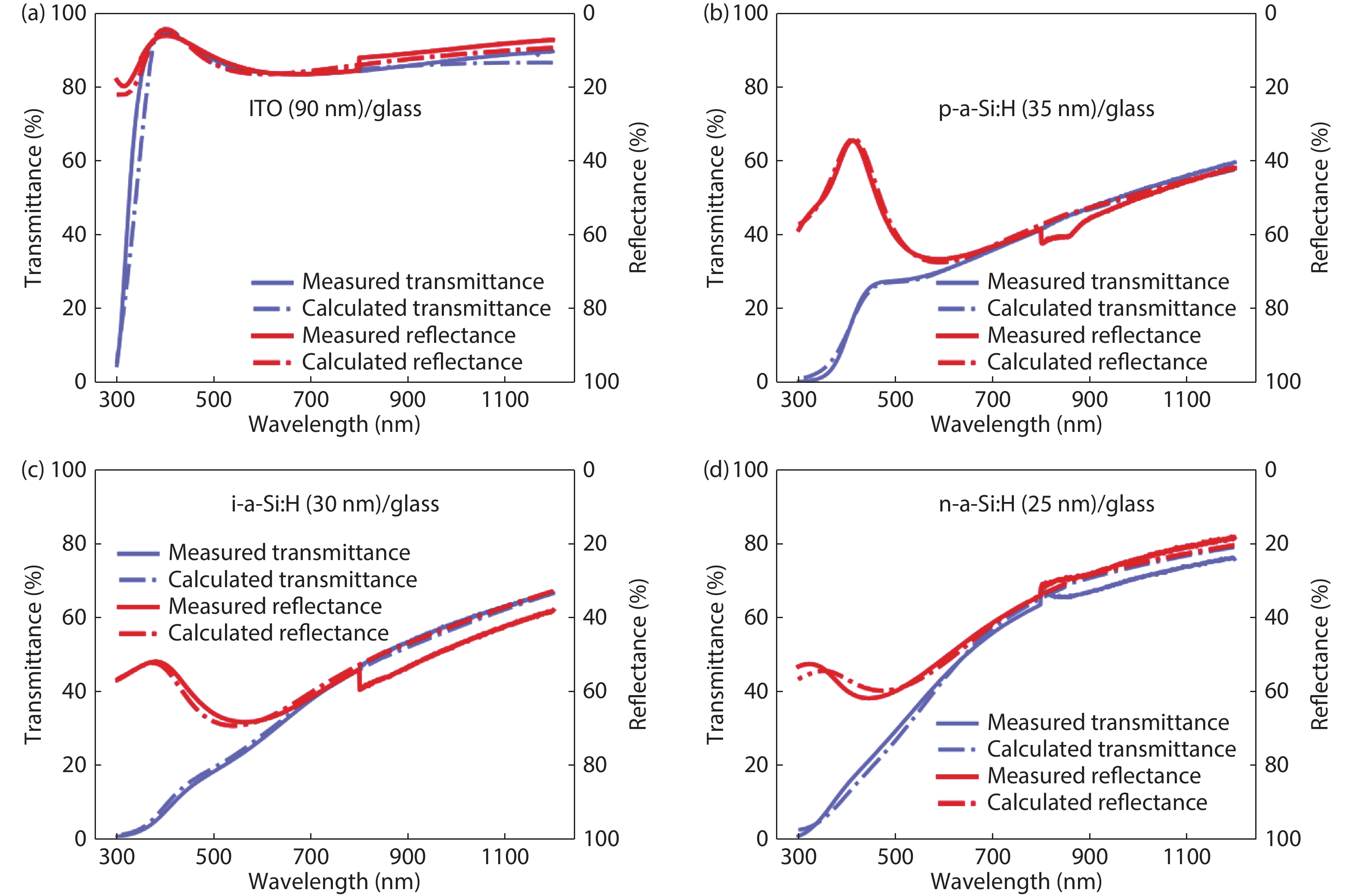
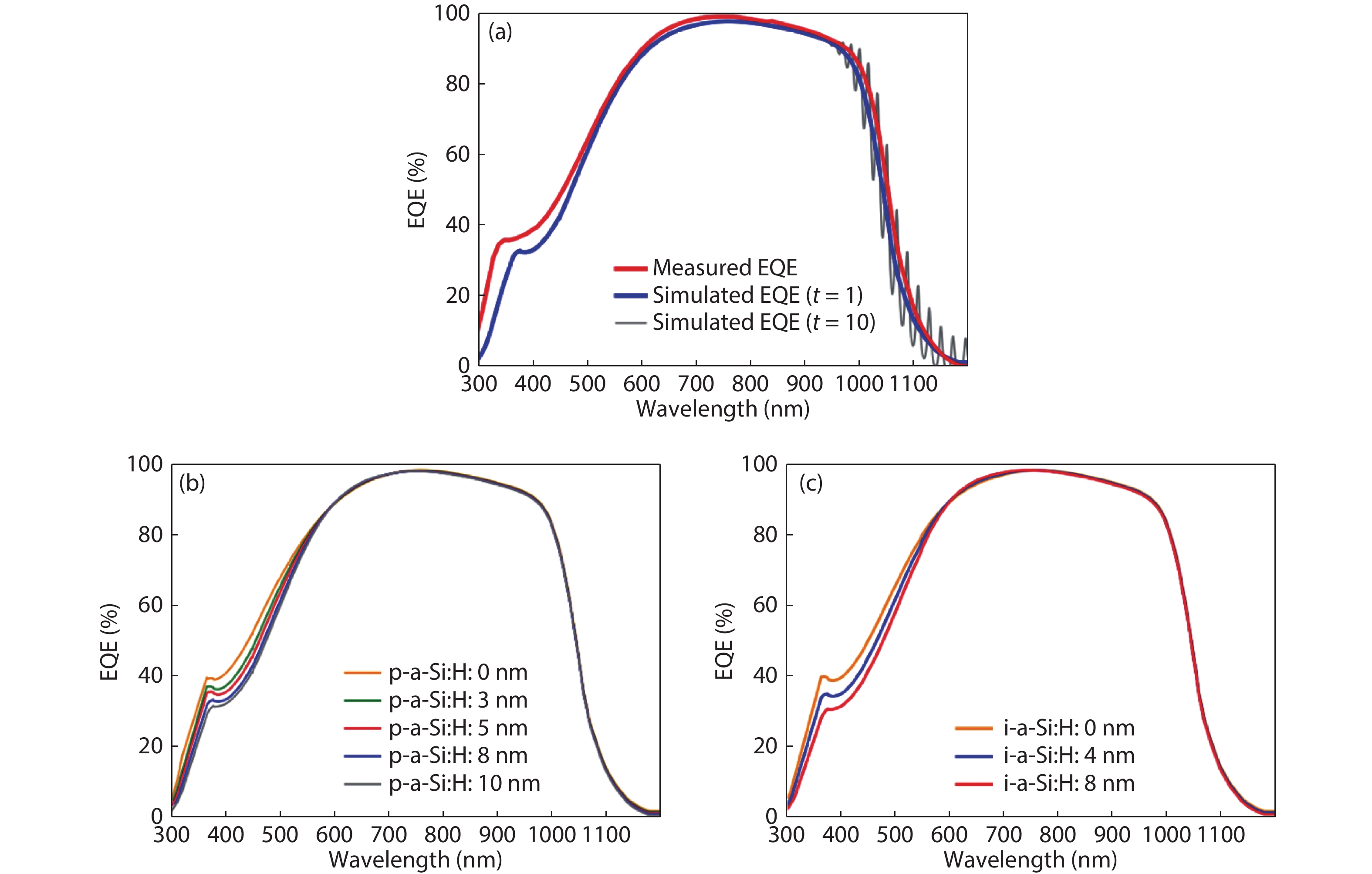
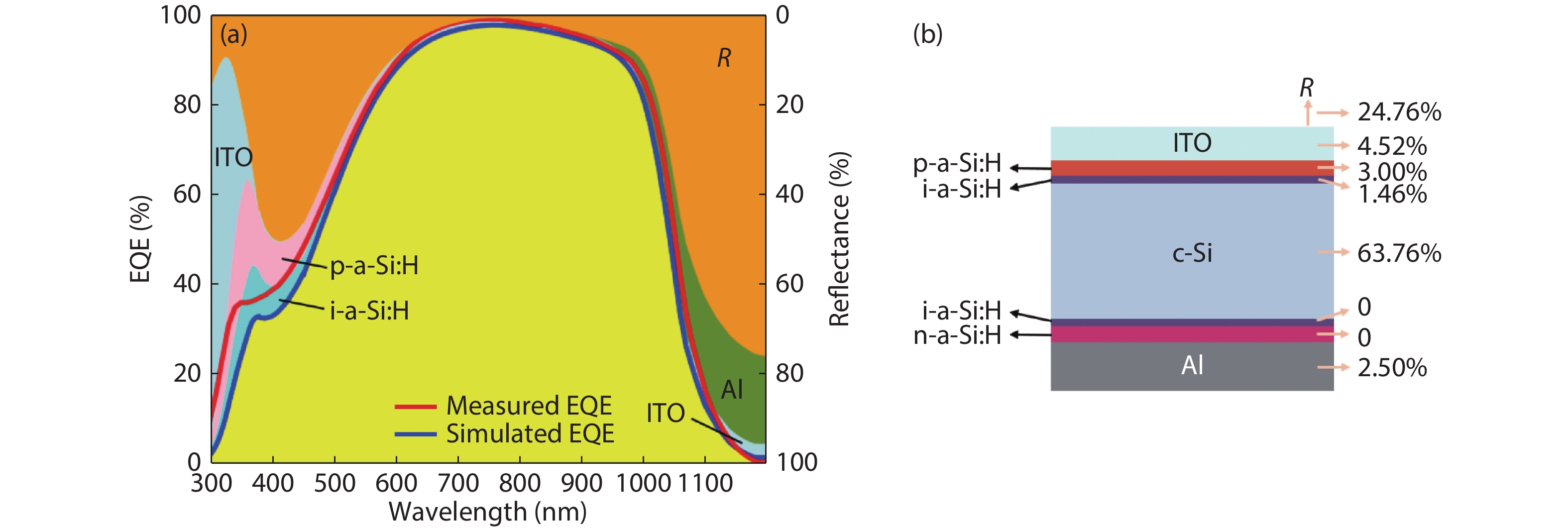
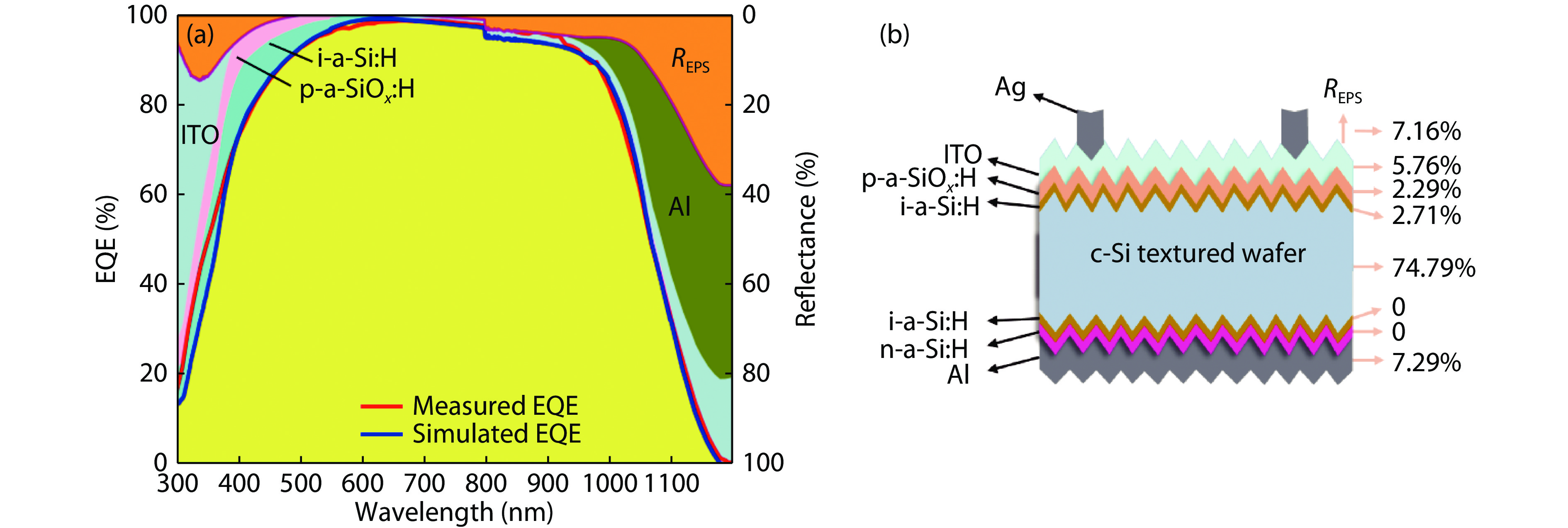
2019, 40(12): 122701 doi: 10.1088/1674-4926/40/12/122701

In this study, a method for optical simulation of external quantum efficiency (EQE) spectra of solar cells based on spectroscopy is proposed, which is based on the tested transmittance and reflectance spectra. First, to obtain a more accurate information of refractive index and extinction coefficient


J. Semicond.
2019, 40(12): 122901 doi: 10.1088/1674-4926/40/12/122901
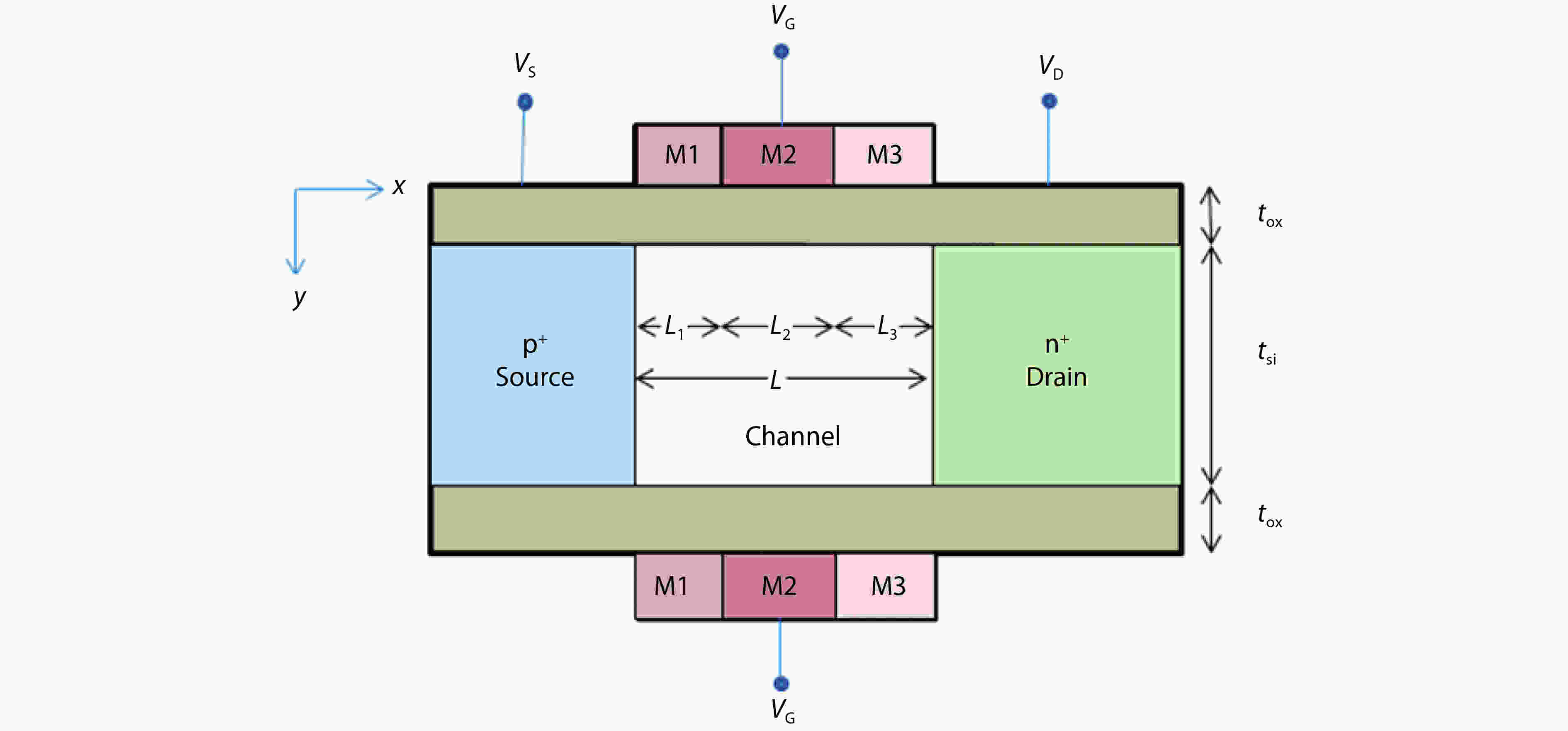
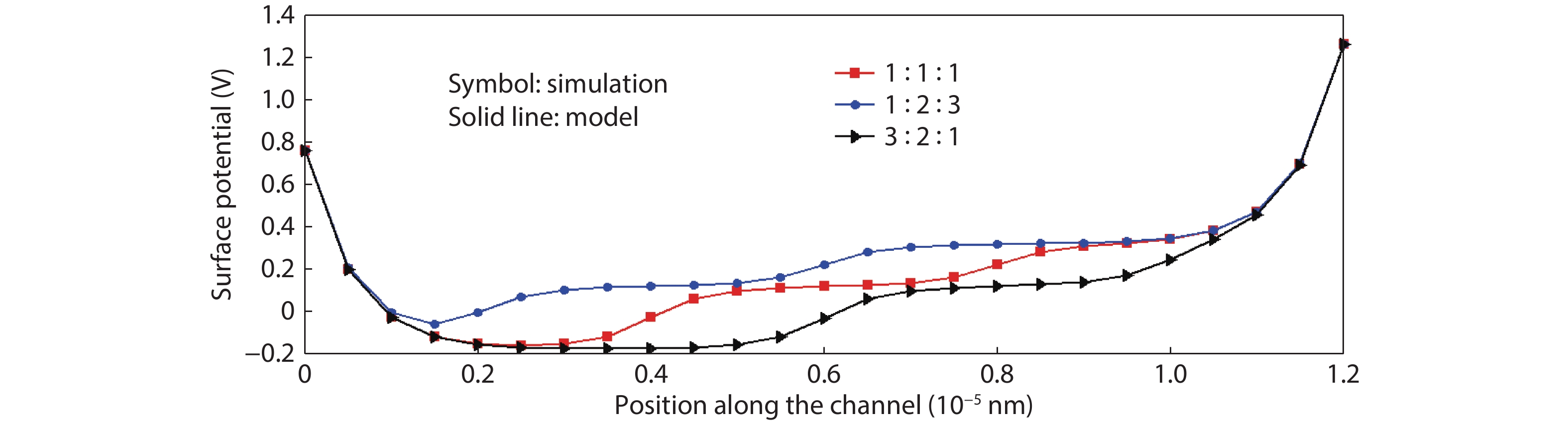
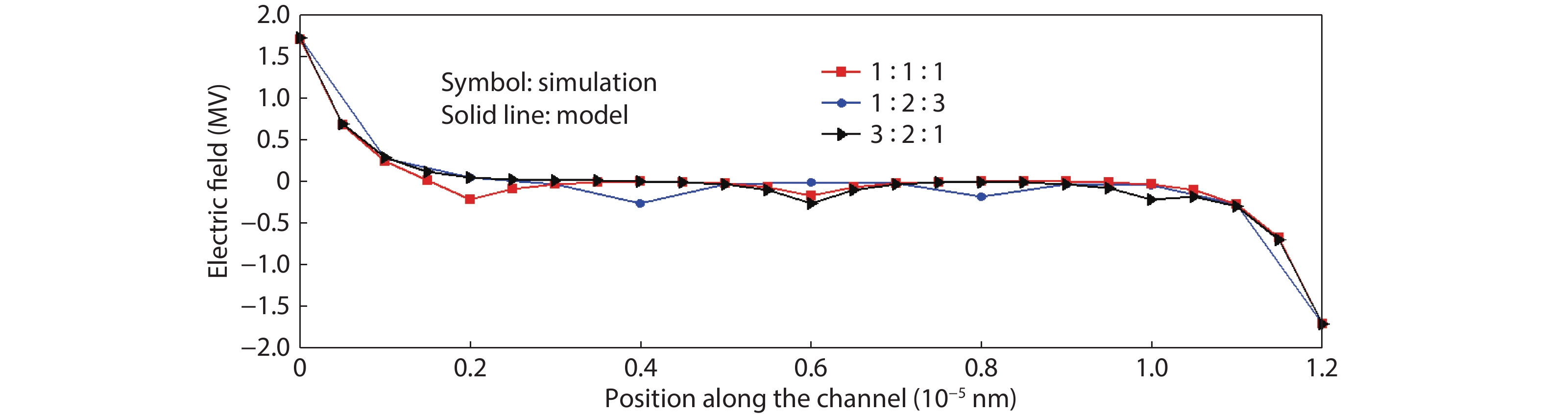
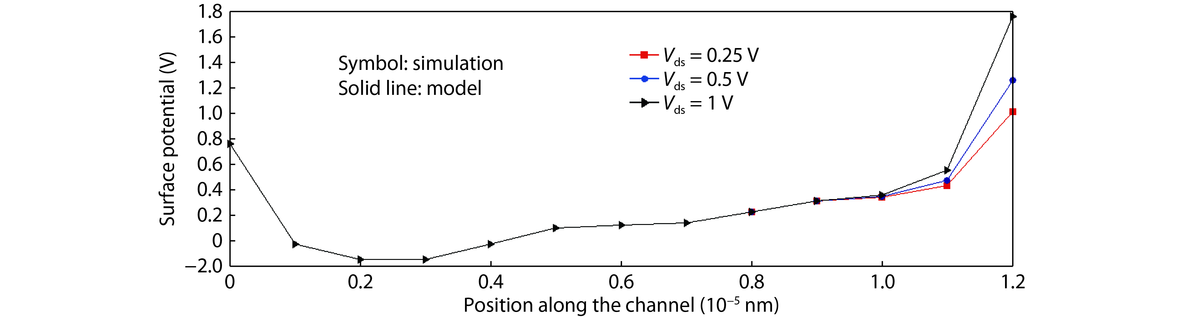
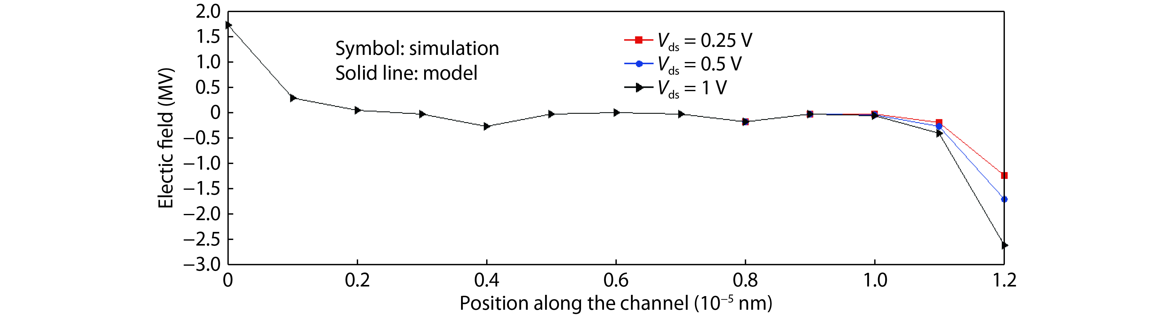
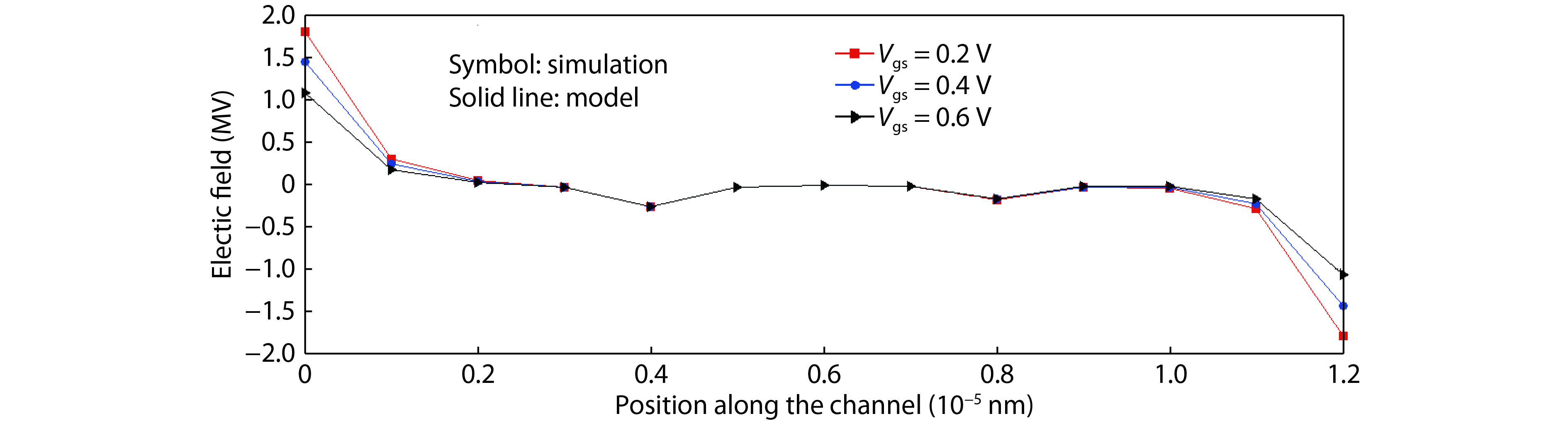
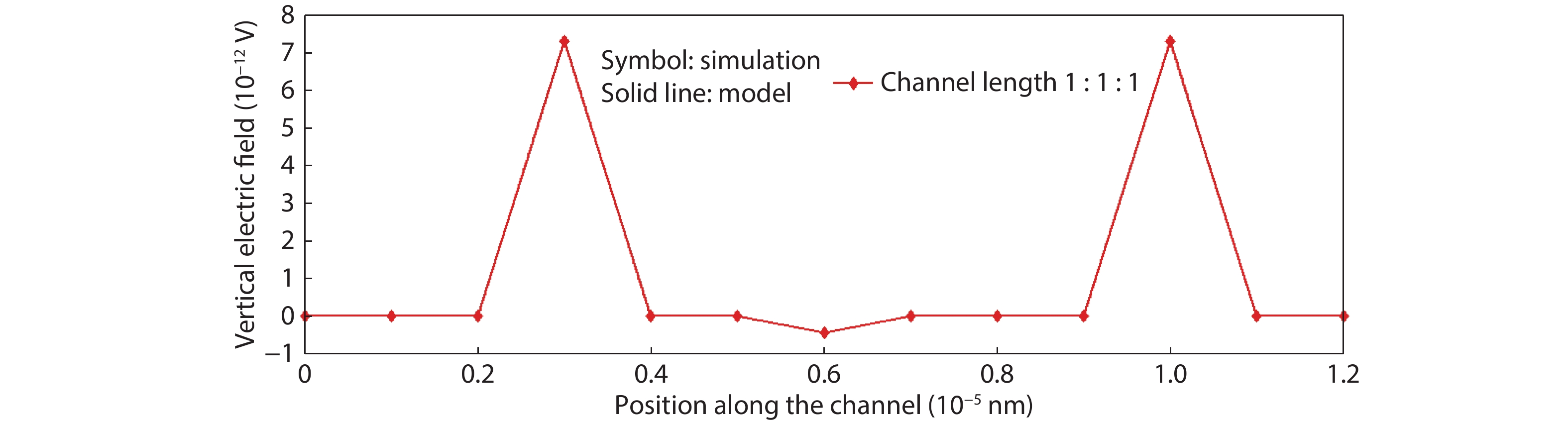
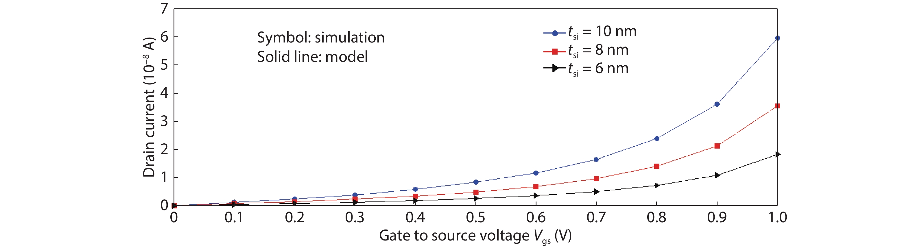
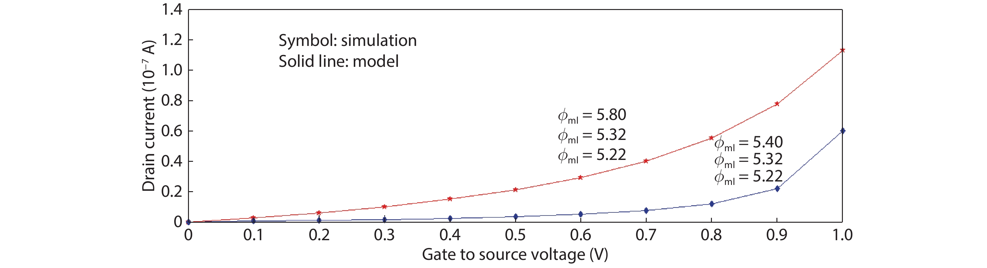
This paper presents a compact two-dimensional analytical device model of surface potential, in addition to electric field of triple-material double-gate (TMDG) tunnel FET. The TMDG TFET device model is developed using a parabolic approximation method in the channel depletion space and a boundary state of affairs across the drain and source. The TMDG TFET device is used to analyze the electrical performance of the TMDG structure in terms of changes in potential voltage, lateral and vertical electric field. Because the TMDG TFET has a simple compact structure, the surface potential is computationally efficient and, therefore, may be utilized to analyze and characterize the gate-controlled devices. Furthermore, using Kane's model, the current across the drain can be modeled. The graph results achieved from this device model are close to the data collected from the technology computer aided design (TCAD) simulation.


J. Semicond.
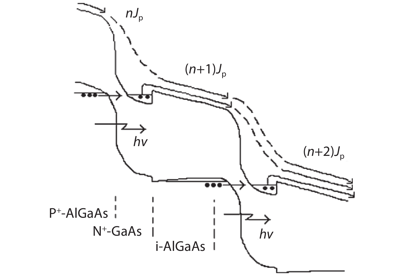
2019, 40(12): 122902 doi: 10.1088/1674-4926/40/12/122902

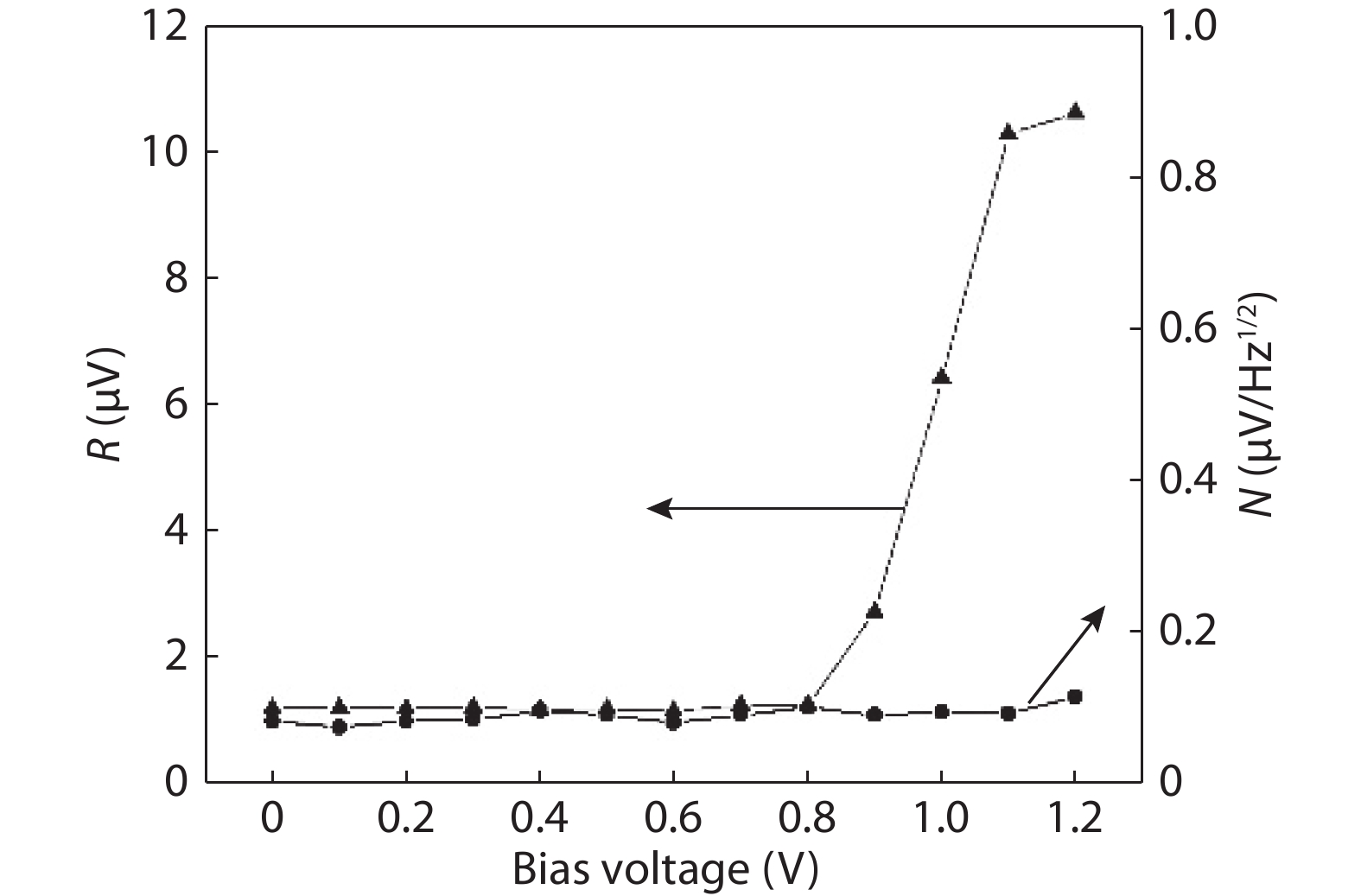
To reduce the difficulty of the epitaxy caused by multiple quantum well infrared photodetector (QWIP) with tunnel compensation structure, an improved structure is proposed. In the new structure, the superlattices are located between the tunnel junction and the barrier as the infrared absorption region, eliminating the effect of doping concentration on the well width in the original structure. Theoretical analysis and experimental verification of the new structure are carried out. The experimental sample is a two-cycle device, each cycle contains a tunnel junction, a superlattice infrared absorption region and a thick barrier. The photosurface of the detector is 200 × 200 μm2 and the light is optically coupled by 45° oblique incidence. The results show that the optimal operating voltage of the sample is –1.1 V, the dark current is 2.99 × 10⁻⁸ A, and the blackbody detectivity is 1.352 × 108 cm·Hz1/2·W–1 at 77 K. Our experiments show that the new structure can work normally.