REVIEWS

Silicon photonic transceivers for application in data centers

Haomiao Wang1, 2, Hongyu Chai1, 2, Zunren Lv1, 2, Zhongkai Zhang1, 2, Lei Meng1, 2, Xiaoguang Yang1, 2 and Tao Yang1, 2,

+ Author Affiliations

 Corresponding author: Tao Yang, Email: tyang@semi.ac.cn

PDF

Turn off MathJax

Abstract: 
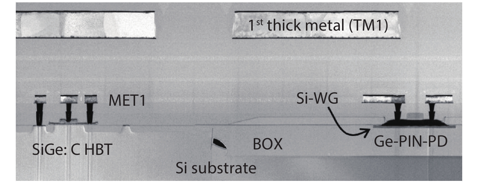
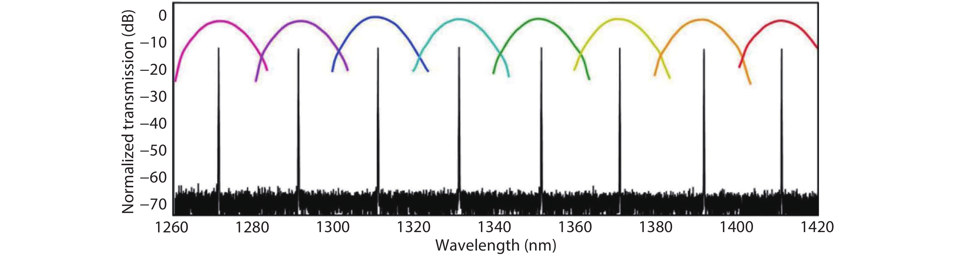
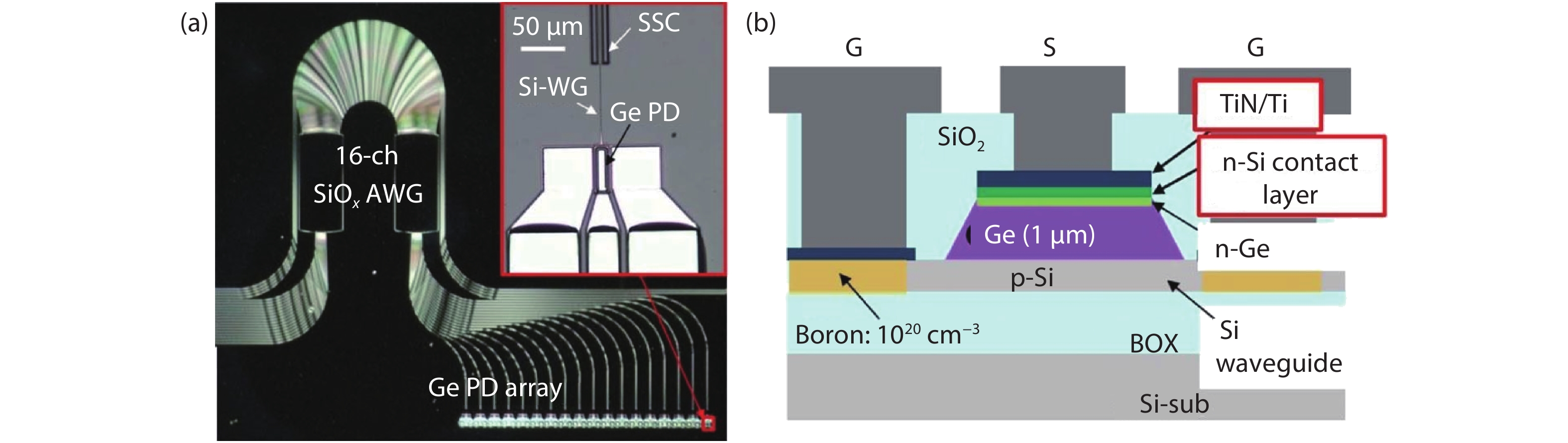
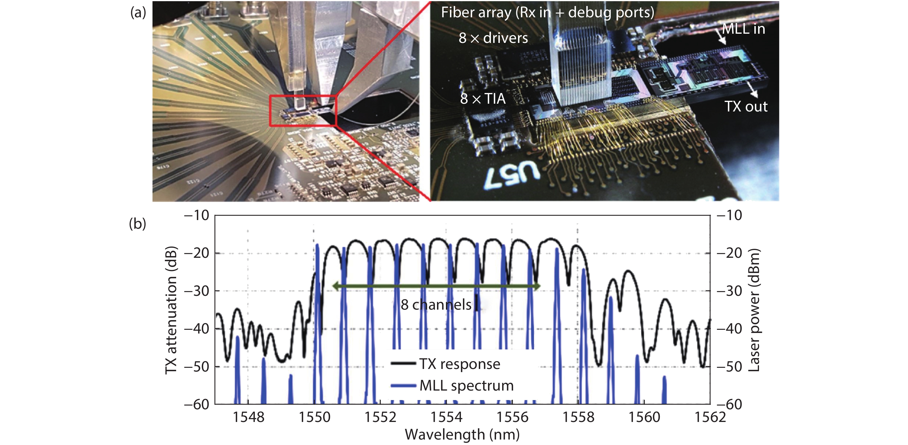
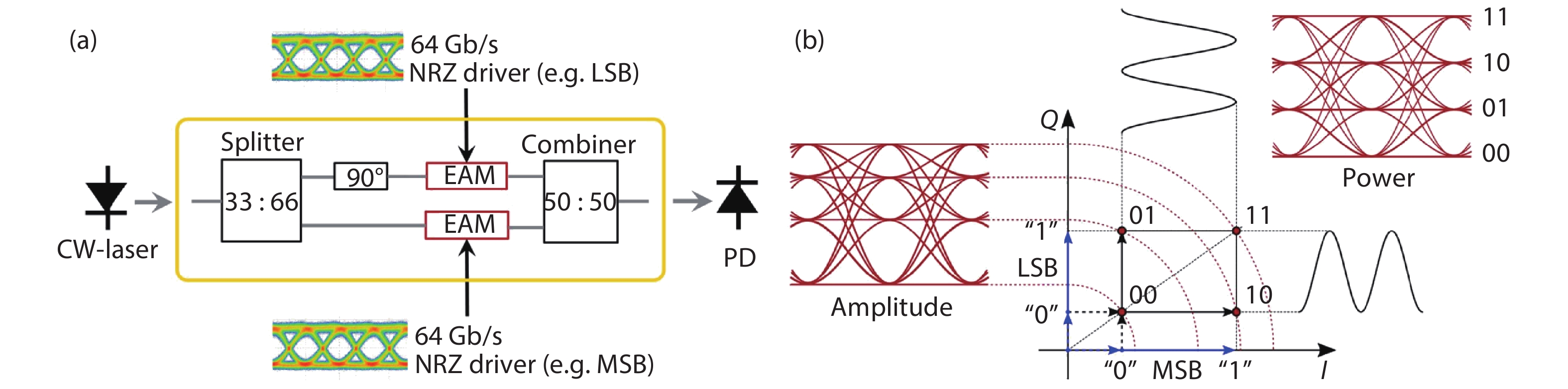
Global data traffic is growing rapidly, and the demand for optoelectronic transceivers applied in data centers (DCs) is also increasing correspondingly. In this review, we first briefly introduce the development of optoelectronics transceivers in DCs, as well as the advantages of silicon photonic chips fabricated by complementary metal oxide semiconductor process. We also summarize the research on the main components in silicon photonic transceivers. In particular, quantum dot lasers have shown great potential as light sources for silicon photonic integration—whether to adopt bonding method or monolithic integration—thanks to their unique advantages over the conventional quantum-well counterparts. Some of the solutions for high-speed optical interconnection in DCs are then discussed. Among them, wavelength division multiplexing and four-level pulse-amplitude modulation have been widely studied and applied. At present, the application of coherent optical communication technology has moved from the backbone network, to the metro network, and then to DCs.

Key words: data centersilicon-based optoelectronic transceiverhigh-speed optical interconnectionquantum dot lasers


[1]
Reinsel D, Gantz J, Rydning J. The digitization of the world-from egde to core. An IDC Whitepaper, 2018
[2]
Jones N. The information factories. Nature, 2018, 561(7722), 163
[3]
Miller D. Device requirements for optical interconnects to silicon chips. Proc IEEE, 2009, 97(7), 1166 doi: 10.1109/JPROC.2009.2014298
[4]
Ohashi K, Nishi K, Shimizu T, et al. On-chip optical interconnect. Proc IEEE, 2009, 97(7), 1186 doi: 10.1109/JPROC.2009.2020331
[5]
Lu Z G, Liu J R, Song C Y, et al. High performance InAs/InP quantum dot 34.462-GHz C-band coherent comb laser module. Opt Express, 2018, 26(2), 2160 doi: 10.1364/OE.26.002160
[6]
Lv Z R, Zhang Z K, Yang X G, et al. Improved performance of 1.3-μm InAs/GaAs quantum dot lasers by direct Si doping. Appl Phys Lett, 2018, 113(1), 011105 doi: 10.1063/1.5026809
[7]
Chen L, Xu Q, Wood M G, et al. Hybrid silicon and lithium niobate electro-optical ring modulator. Optica, 2014, 1(2), 112 doi: 10.1364/OPTICA.1.000112
[8]
Wang C, Zhang M, Chen X, et al. Integrated lithium niobate electro-optic modulators operating at CMOS-compatible voltages. Nature, 2018, 562(7725), 101 doi: 10.1038/s41586-018-0551-y
[9]
Liao S, Feng N N, Feng D. 36 GHz submicron silicon waveguide germanium photodetector. Opt Express, 2011, 19(11), 10967 doi: 10.1364/OE.19.010967
[10]
Chen L, Doerr C R, Chen Y K, et al. Low-loss and broadband cantilever couplers between standard cleaved fibers and high-index-contrast Si3N4 or Si waveguides. IEEE Photonics Technol Lett, 2010, 22(23), 1744 doi: 10.1109/LPT.2010.2085040
[11]
Pinguet T, Denton S, Gloeckner S, et al. High-volume manufacturing platform for silicon photonics. Proc IEEE, 2018, 106(12), 2281 doi: 10.1109/JPROC.2018.2859198
[12]
Deng Q Z, Liu L, Zhang R, et al. Athermal and flat-topped silicon Mach-Zehnder filters. Opt Express, 2016, 24(26), 29577 doi: 10.1364/OE.24.029577
[13]
Hiraki T, Nishi H, Tsuchizawa T, et al. Si–Ge–silica monolithic integration platform and its application to a 22-Gb/s × 16-ch WDM receiver. IEEE Photonics J, 2013, 5(4), 4500407 doi: 10.1109/JPHOT.2013.2269676
[14]
Mekis A, Gloeckner S, Masini G, et al. A grating-coupler-enabled CMOS photonics platform. IEEE J Sel Top Quantum Electron, 2011, 17(3), 597 doi: 10.1109/JSTQE.2010.2086049
[15]
Winn J N, Rusin D, Kochanek C S. A high-speed silicon optical modulator based on a metal-oxide-semiconducor capacitor. Nature, 2004, 427(6975), 613 doi: 10.1038/nature02279
[16]
DeRose C T, Trotter D C, Zortman W A, et al. Ultra compact 45 GHz CMOS compatible Germanium waveguide photodiode with low dark current. Opt Express, 2011, 19(25), 24897 doi: 10.1364/OE.19.024897
[17]
Ennen H, Schneider J, Pomrenke G, et al. 1.54-μm luminescence of erbium-implanted III–V semiconductors and silicon. Appl Phys Lett, 1983, 43(10), 943 doi: 10.1063/1.94190
[18]
Wirths S, Geiger R, von den Driesch N, et al. Lasing in direct-bandgap GeSn alloy grown on Si. Nat Photonics, 2015, 9(2), 88 doi: 10.1038/nphoton.2014.321
[19]
d'Avezac M, Luo J W, Chanier T, et al. Genetic-algorithm discovery of a direct-gap and optically allowed superstructure from indirect-gap Si and Ge semiconductors. Phys Rev Lett, 2012, 108(2), 027401 doi: 10.1103/PhysRevLett.108.027401
[20]
Camacho-Aguilera R E, Cai Y, Patel N, et al. An electrically pumped germanium laser. Opt Express, 2012, 20(10), 11316 doi: 10.1364/OE.20.011316
[21]
Zhou Z, Yin B, Michel J. On-chip light sources for silicon photonics. Light: Sci Appl, 2015, 4(11), e358 doi: 10.1038/lsa.2015.131
[22]
Kobayashi N, Sato K, Namiwaka M, et al. Silicon photonic hybrid ring-filter external cavity wavelength tunable lasers. J Lightwave Technol, 2015, 33(6), 1241 doi: 10.1109/JLT.2014.2385106
[23]
Wang T, Liu H. 1.3-μm InAs/GaAs quantum-dot lasers monolithically grown on Si substrates. Opt Express, 2011, 19(12), 11381 doi: 10.1364/OE.19.011381
[24]
Chen S, Li W, Wu J, et al. Electrically pumped continuous-wave III–V quantum dot lasers on silicon. Nat Photonics, 2016, 10(5), 307 doi: 10.1038/nphoton.2016.21
[25]
Li Q, Ng K W, Lau K M. Growing antiphase-domain-free GaAs thin films out of highly ordered planar nanowire arrays on exact (001) silicon. Appl Phys Lett, 2015, 106(7), 072105 doi: 10.1063/1.4913432
[26]
Schulze C S, Huang X, Prohl C, et al. Atomic structure and stoichiometry of In(Ga)As/GaAs quantum dots grown on an exact-oriented GaP/Si(001) substrate. Appl Phys Lett, 2016, 108(14), 143101 doi: 10.1063/1.4945598
[27]
Wan Y, Li Q, Geng Y, et al. InAs/GaAs quantum dots on GaAs-on-V-grooved-Si substrate with high optical quality in the 1.3 μm band. Appl Phys Lett, 2015, 107(8), 081106 doi: 10.1063/1.4929441
[28]
Fang A W, Park H, Bowers J E. Electrically pumped hybrid AlGaInAs–silicon evanescent laser. Opt Express, 2006, 14(20), 9203 doi: 10.1364/OE.14.009203
[29]
Zhang C, Bowers J E. Silicon photonic terabit/s network-on-chip for datacenter interconnection. Opt Fiber Technol, 2018, 44, 2 doi: 10.1016/j.yofte.2017.12.007
[30]
Agrell E, Karlsson M, Chraplyvy A R, et al. Roadmap of optical communications. J Opt, 2016, 18(6), 063002 doi: 10.1088/2040-8978/18/6/063002
[31]
Urino Y, Usuki T, Fujikata J, et al. High-density and wide-bandwidth optical interconnects with silicon optical interposers. Photonics Res, 2014, 2(3), A1 doi: 10.1364/PRJ.2.0000A1
[32]
Shimizu T, Hatori N, Arakawa Y. High density hybrid integrated light source with a laser diode array on a silicon optical waveguide platform for inter-chip optical interconnection. Group IV Photonics, 2011, 181
[33]
Jang B, Tanabe K, Kako S, et al. A hybrid silicon evanescent quantum dot laser. Appl Phys Express, 2016, 9(9), 092102 doi: 10.7567/APEX.9.092102
[34]
Wang H, Kim D, Harfouche M, et al. Narrow-linewidth oxide-confined heterogeneously integrated Si/III–V semiconductor lasers. IEEE Photonics Technol Lett, 2017, 29(24), 2199 doi: 10.1109/LPT.2017.2771222
[35]
Arakawa Y, Sakaki H. Multidimensional quantum well laser and temperature dependence of its threshold current. Appl Phys Lett, 1982, 40(11), 939 doi: 10.1063/1.92959
[36]
Sugawara M, Usami M. Handiling the heat QD-lasers. Nat Photonics, 2009, 3, 30 doi: 10.1038/nphoton.2008.267
[37]
Nishi K, Saito H, Sugou S, et al. A narrow photoluminescence linewidth of 21 meV at 1.35 μm from strain-reduced InAs quantum dots covered by In0.2Ga0.8As grown on GaAs substrates. Appl Phys Lett, 1999, 74(8), 1111 doi: 10.1063/1.123459
[38]
Nishi K, Takemasa K, Sugawara M, et al. Development of quantum dot lasers for data-com and silicon photonics applications. IEEE J Sel Top Quantum Electron, 2017, 23(6), 1 doi: 10.1109/JSTQE.2017.2699787
[39]
Takada K, Tanaka Y, Matsumoto T, et al. Wide-temperature-range 10.3 Gbit/s operations of 1.3 μm high-density quantum-dot DFB lasers. Electron Lett, 2011, 47(3), 206 doi: 10.1049/el.2010.3312
[40]
Akrout A, Shen A, Brenot R, et al. Separate error-free transmission of eight channels at 10 Gb/s using comb generation in a quantum-dash-based mode-locked laser. IEEE Photonics Technol Lett, 2009, 21(23), 1746 doi: 10.1109/LPT.2009.2032243
[41]
O'Brien D, Hegarty S P, Huyet G, et al. Sensitivity of quantum-dot semiconductor lasers to optical feedback. Opt Lett, 2004, 29(10), 1072 doi: 10.1364/OL.29.001072
[42]
Zhou Y G, Zhou C, Cao C F, et al. Relative intensity noise of InAs quantum dot lasers epitaxially grown on Ge. Opt Express, 2017, 25(23), 28817 doi: 10.1364/OE.25.028817
[43]
Liao M, Chen S, Park J S, et al. III–V quantum-dot lasers monolithically grown on silicon. Semicond Sci Technol, 2018, 33(12), 123002 doi: 10.1088/1361-6641/aae6a5
[44]
[45]
Jung D, Norman J, Kennedy M J, et al. High efficiency low threshold current 1.3 μm InAs quantum dot lasers on on-axis (001) GaP/Si. Appl Phys Lett, 2017, 111(12), 122107 doi: 10.1063/1.4993226
[46]
Shi B, Wang L, Taylor A A, et al. MOCVD grown low dislocation density GaAs-on-V-groove patterned (001) Si for 1.3 μm quantum dot laser applications. Appl Phys Lett, 2019, 114(17), 172102 doi: 10.1063/1.5090437
[47]
Wei W Q, Wang J H, Zhang B, et al. InAs QDs on (111)-faceted Si (001) hollow substrates with strong emission at 1300 nm and 1550 nm. Appl Phys Lett, 2018, 113(5), 053107 doi: 10.1063/1.5043169
[48]
Ward T, Sánchez A M, Tang M, et al. Design rules for dislocation filters. J Appl Phys, 2014, 116(6), 063508 doi: 10.1063/1.4892162
[49]
Volz K, Beyer A, Witte W, et al. GaP-nucleation on exact Si (001) substrates for III/V device integration. J Cryst Growth, 2011, 315(1), 37 doi: 10.1016/j.jcrysgro.2010.10.036
[50]
Alcotte R, Martin M, Moeyaert J, et al. Epitaxial growth of antiphase boundary free GaAs layer on 300 mm Si (001) substrate by metalorganic chemical vapour deposition with high mobility. APL Mater, 2016, 4(4), 046101 doi: 10.1063/1.4945586
[51]
Zhang B, Wei W Q, Wang J H, et al. O-band InAs/GaAs quantum-dot microcavity laser on Si (001) hollow substrate by in-situ hybrid epitaxy. AIP Adv, 2019, 9(1), 015331 doi: 10.1063/1.5065527
[52]
Jung D, Callahan P G, Shin B, et al. Low threading dislocation density GaAs growth on on-axis GaP/Si (001). J Appl Phys, 2017, 122(22), 225703 doi: 10.1063/1.5001360
[53]
Lee A D, Jiang Q, Tang M C, et al. InAs/GaAs quantum-dot lasers monolithically grown on Si, Ge, and Ge-on-Si substrates. IEEE J Sel Top Quantum Electron, 2013, 19(4), 1901107 doi: 10.1109/JSTQE.2013.2247979
[54]
Akiyama M, Kawarada Y, Ueda T, et al. Growth of high quality GaAs layers on Si substrate by MOCVD. J Cryst Growth, 1986, 77, 490 doi: 10.1016/0022-0248(86)90342-8
[55]
Tang M, Chen S, Wu J, et al. 1.3-μm InAs/GaAs quantum-dot lasers monolithically grown on Si substrates using InAlAs/GaAs dislocation filter layers. Opt Express, 2014, 22(10), 11528 doi: 10.1364/OE.22.011528
[56]
Li W, Chen S, Tang M, et al. Effect of rapid thermal annealing on threading dislocation density in III–V epilayers monolithically grown on silicon. J Appl Phys, 2018, 123(21), 215303 doi: 10.1063/1.5011161
[57]
Wan Y, Inoue D, Jung D, et al. Directly modulated quantum dot lasers on silicon with a milliampere threshold and high temperature stability. Photonics Res, 2018, 6(8), 776 doi: 10.1364/PRJ.6.000776
[58]
Urino Y, Shimizu T, Okano M, et al. First demonstration of high density optical interconnects integrated with lasers, optical modulators and photodetectors on single silicon substrate. Opt Express, 2011, 19(26), B159 doi: 10.1364/OE.19.00B159
[59]
Thomson D J, Gardes F Y, Fedeli J M, et al. 50-Gb/s silicon optical modulator. IEEE Photonics Technol Lett, 2012, 24(4), 234 doi: 10.1109/LPT.2011.2177081
[60]
Witzens J. High-speed silicon photonics modulators. Proc IEEE, 2018, 106(12), 2158 doi: 10.1109/JPROC.2018.2877636
[61]
Ziebell M, Marris-Morini D, Rasigade G, et al. 40 Gbit/s low-loss silicon optical modulator based on a pipin diode. Opt Express, 2012, 20(10), 10591 doi: 10.1364/OE.20.010591
[62]
Timurdogan E, Sorace-Agaskar C M, Sun J, et al. An ultralow power athermal silicon modulator. Nat Commun, 2014, 5, 4008 doi: 10.1038/ncomms5008
[63]
Debnath K, Thomson D J, Zhang W, et al. All-silicon carrier accumulation modulator based on a lateral metal–oxide–semiconductor capacitor. Photonics Res, 2018, 6(5), 373 doi: 10.1364/PRJ.6.000373
[64]
Ishikawa Y, Wada K, Liu J, et al. Strain-induced enhancement of near-infrared absorption in Ge epitaxial layers grown on Si substrate. J Appl Phys, 2005, 98(1), 013501 doi: 10.1063/1.1943507
[65]
Ishikawa Y, Wada K, Cannon D D, et al. Strain-induced band gap shrinkage in Ge grown on Si substrate. Appl Phys Lett, 2003, 82(13), 2044 doi: 10.1063/1.1564868
[66]
Yin T, Cohen R. 31GHz Ge n–i–p waveguide photodetectors on silicon-on-insulator substrate. Opt Express, 2007, 15(21), 13965 doi: 10.1364/OE.15.013965
[67]
Dehlinger G, Koester S J, Schaub J D, et al. High-speed germanium-on-SOI lateral PIN photodiodes. IEEE Photonics Technol Lett, 2004, 16(11), 2547 doi: 10.1109/LPT.2004.835631
[68]
Lischke S, Knoll D, Mai C, et al. High bandwidth, high responsivity waveguide-coupled germanium p–i–n photodiode. Opt Express, 2015, 23(21), 27213 doi: 10.1364/OE.23.027213
[69]
Pathak S, Dumon P, Van Thourhout D, et al. Comparison of AWGs and echelle gratings for wavelength division multiplexing on silicon-on-insulator. IEEE Photonics J, 2014, 6(5), 1 doi: 10.1109/jphot.2014.2361658
[70]
Jeong S H, Tanaka Y. Silicon-wire optical demultiplexers based on multistage delayed Mach-Zehnder interferometers for higher production yield. Appl Opt, 2018, 57(22), 6474 doi: 10.1364/AO.57.006474
[71]
Pathak S, Vanslembrouck M, Dumon P, et al. Optimized silicon AWG with flattened spectral response using an MMI aperture. J Lightwave Technol, 2013, 31(1), 87 doi: 10.1109/JLT.2012.2231399
[72]
Urino Y, Hatori N, Mizutani K, et al. First demonstration of athermal silicon optical interposers with quantum dot lasers operating up to 125 °C. J Lightwave Technol, 2015, 33(6), 1223 doi: 10.1109/JLT.2014.2380811
[73]
Kurata K, Suzuki Y, Kurihara M, et al. Prospect of chip scale silicon photonics transceiver for high density multi-mode wiring system. Opt Commun, 2016, 362, 36 doi: 10.1016/j.optcom.2015.10.027
[74]
Yashiki K, Uemura T, Kurihara M, et al. 25-Gbps/ch error-free operation over 300-m MMF of low-power-consumption silicon-photonics-based chip-scale optical I/O cores. IEICE Trans Electron, 2016, E99.C(2), 148 doi: 10.1587/transele.E99.C.148
[75]
Nakamura T, Yashiki K, Mizutani K, et al. Fingertip-size optical module, optical io core, and its application in FPGA. 2019 the Institude of Electronics, Information and Communication Engineers, 2019, E102-C(4), 333
[76]
Aoki T, Sekiguchi S, Simoyama T, et al. Low-crosstalk simultaneous 16-channel × 25 Gb/s operation of high-density silicon photonics optical transceiver. J Lightwave Technol, 2018, 36(5), 1262 doi: 10.1109/JLT.2018.2797167
[77]
Srivastava A K, De Dobbelaere P, Armijo G, et al. Silicon-photonics-based optical transceivers for high-speed interconnect applications. In: Next-Generation Optical Networks for Data Centers and Short-Reach Links III, 2016, 9775, 977503
[78]
Meister S, Grehn M, Rhee H, et al. Silicon photonics for 100 Gbit/s intra-data center optical interconnects. In: Optical Interconnects XVI, 2016, 9753, 975308
[79]
Kupijai S, Rhee H, Al-Saadi A, et al. 25 Gb/s silicon photonics interconnect using a transmitter based on a node-matched-diode modulator. J Lightwave Technol, 2016, 34(12), 2920 doi: 10.1109/JLT.2015.2489840
[80]
Intel® silicon photonics 100G PSM4 optical transceiver brief. 2017
[81]
Intel® silicon photonics 100G CWDM4 optical transceiver brief. 2017
[82]
Driscoll J B, Doussiere P, Islam S. First 400G 8-channel CWDM silicon photonic integrated transmitter. 2018 IEEE 15th International Conference on Group IV Photonics (GFP), 2018
[83]
Moscoso-Martir A, Tabatabaei-Mashayekh A, Muller J, et al. 8-channel WDM silicon photonics transceiver with SOA and semiconductor mode-locked laser. Opt Express, 2018, 26(19), 25446 doi: 10.1364/OE.26.025446
[84]
Verbist J, Lambrecht J, Verplaetse M, et al. Real-time and DSP-free 128 Gb/s PAM-4 link using a binary driven silicon photonic transmitter. J Lightwave Technol, 2019, 37(2), 274 doi: 10.1109/JLT.2018.2877461
[85]
Doerr C R, Chen L. Monolithic PDM-DQPSK receiver in silicon. 2010 36th European Conference and Exhibition on Optical Communication (Ecoc), 2010
[86]
Doerr C, Chen L, Vermeulen D, et al. Single-chip silicon photonics 100-Gbs coherent transceiver. Optical Fiber Communication Conference: Postdeadline Papers, 2014
[87]
Zhang Z, Li C, Chen J, et al. Coherent transceiver operating at 61-Gbaud/s. Opt Express, 2015, 23(15), 18988 doi: 10.1364/OE.23.018988
[88]
IEEE Standard for Ethernet. IEEE 802.3bs, 2017
[89]
Shin S M, Kim H B. Fabrication of 53 Gb/s optical transceiver over 40-km transmission with PAM4 modulation. International Conference on Advanced Communications Technology, 2019
[90]
Depaoli E, Zhang H, Mazzini M, et al. A 64 Gb/s low-power transceiver for short-reach PAM-4 electrical links in 28-nm FDSOI CMOS. IEEE J Solid-State Circuits, 2019, 54(1), 6 doi: 10.1109/JSSC.2018.2873602
[91]
SiFotonics Technologies & Products Brochure
[92]
Nagarajan R, Bhoja S, Issenhuth T. 100 Gbit/s, 120 km, PAM 4 based switch to switch, layer 2 silicon photonics based optical interconnects for datacenters. Hot Chips 28 Symposium, 2016
[93]
Doerr C R, Fontaine N K, Buhl L L. PDM-DQPSK silicon receiver with integrated monitor and minimum number of controls. IEEE Photonics Technol Lett, 2012, 24(8), 697 doi: 10.1109/LPT.2012.2187048
[94]
Po D, Xiang L, Chandrasekhar S, et al. Monolithic silicon photonic integrated circuits for compact 100+Gb/s coherent optical receivers and transmitters. IEEE J Sel Top Quantum Electron, 2014, 20(4), 150 doi: 10.1109/JSTQE.2013.2295181
[95]
Sepehrian H, Lin J, Rusch L A, et al. Silicon photonic IQ modulators for 400 Gb/s and beyond. J Lightwave Technol, 2019, 37(13), 3078 doi: 10.1109/JLT.2019.2910491
[96]
Cheng J, Xie C, Chen Y, et al. Comparision of coherent and IMDD transceivers for intra datacenter optical interconnets. Optical Fiber Communication Conference 2019, 2019
Fig. 1.  (Color online) Forecast of global data traffic and electricity in ICT[1, 2].

Fig. 2.  (Color online) Three coupling modes of silicon-based III–V lasers: (a) lens coupling[11], (b) edge coupling[32], (c) evanescent coupling[33].

Fig. 3.  (Color online) Comparison of typical power–current characteristics of FP lasers. QD-LD (left) is insensitive to temperature and has an almost constant threshold current and slope efficiency. Other two pictures (right two) show the characteristics of two typical QW-LDs[36].

Fig. 4.  (a) TEM image of GaAs/Si interface generating a large number of dislocations[43]. (b) The TDs density gradually decreased after DFLs[24].

Fig. 5.  (Color online) (a) Schematic and TEM images of interaction between QDs and TDs[24]. (b) Room temperature PL spectra of InAs/GaAs QDs grown on GaAs and Si (001) substrates shows that PL peak intensity of QDs grown on Si (001) substrates is stronger, and the inset is an AFM image of a surface InAs/GaAs QDs 1 × 1 μm2 grown on Si (001)[47].

Fig. 6.  (Color online) (a) Diagram of Ridge QD-LD reported by UCL university[24]. (b) Schematic diagram of ring structure QD-LD, SEM top view and infrared imaging reported by UCSB University[30].

Fig. 7.  (Color online) Three types of silicon-based modulators: (a) PIN[31], (b) PN[59], (c) MOS[63].

Fig. 8.  (Color online) (a) Ridge waveguide PD designed by Intel Corp.[66]. (b) Electrode-biased Ge waveguide PD by Kotura[9]. (c) Ge PD was made by BiCMOS process, which increased the ratio of intrinsic region width to doped region width[68].

Fig. 9.  (Color online) (a) Device structures of 1 × 4 Ch optical (De)MUX with different waveguide width[70]. (b) Microsoft image of fabricated 12 × 400 GHz MMI-AWG[71].

Fig. 10.  (Color online) (a) Image of athermal Si optical interposer with close-ups of the components. (b) 20 Gb/s eye diagram with continuous temperature change from 25 to 125 °C[72].

Fig. 11.  (Color online) (a) Photographs of the transmitter and receiver optical I/O core. (b) Cross section of the transmitter and receiver optical I/O core[73].

Fig. 12.  (Color online) Schematic structure of a 16-channel × 25 Gb/s silicon photonic optical transceiver on a package substrate. EIC and PIC are bonded together by solder bumps and mounted on a glass ceramic interposer (GCIP)[76].

Fig. 13.  (Color online) (a) EIC and (b) PIC photographs of a high-density 16-channel optical transceiver[76].

Fig. 14.  (Color online) This silicon interposer integrated the beam splitters to increase the number of interconnect channels[57].

Fig. 15.  (Color online) (a) Generic transceiver architecture of the N × 25 G Luxtera product. (b) Photograph of assembled 8 × 25 G chipset (without fiber array), including: EIC, LaMP and PIC[11].

Fig. 16.  Cross section of co-integrated optical and electronic structures on the chip[78].

Fig. 17.  (Color online) (a) Photograph of Sicoya’s EPIC transceiver[78]. (b) Illustration of NMD modulator. Its mirrors are formed by two 1D-photonic crystals, and the p+, n+ doped areas are located in the nodes of the resonator standing wave[78].

Fig. 18.  (Color online) 8 channels of the Si MUX passband overlaid with the normalized output spectra of the CWDM8 transmitter[82].

Fig. 19.  (Color online) (a) Top view of demultiplexer, 16-ch AWG and Ge PD array. (b) Cross section of Ge PD[13].

Fig. 20.  (Color online) (a) Photograph of transceiver board with optical I/O and only two fibers are used in the fiber array during system test. (b) Tx transmission and filtered MLL spectra at 25 °C and 257 mA showing 8 RRMs aligned within the passband of the filter[83].

Fig. 21.  (Color online) (a) Two-bit optical DAC consisting of two EAMs. (b) Vector and eye diagram of the proposed topology optical PAM-4 generator[84].

Fig. 22.  (Color online) Pluggable QSFP28 module which combine 4 × 25 Gb/s channels into two 50 Gb/s PAM-4 streams[92].

Fig. 23.  (Color online) Block diagram of silicon photonic coherent PIC demonstrated by Acacia[86].

Fig. 24.  (Color online) (a) BER against required total laser power for coherent and IMDD systems. (b) Estimated ASIC power consumption for PAM4, CAP16, DMT and coherent schemes based on 5 nm CMOS[96].

[1]
Reinsel D, Gantz J, Rydning J. The digitization of the world-from egde to core. An IDC Whitepaper, 2018
[2]
Jones N. The information factories. Nature, 2018, 561(7722), 163
[3]
Miller D. Device requirements for optical interconnects to silicon chips. Proc IEEE, 2009, 97(7), 1166 doi: 10.1109/JPROC.2009.2014298
[4]
Ohashi K, Nishi K, Shimizu T, et al. On-chip optical interconnect. Proc IEEE, 2009, 97(7), 1186 doi: 10.1109/JPROC.2009.2020331
[5]
Lu Z G, Liu J R, Song C Y, et al. High performance InAs/InP quantum dot 34.462-GHz C-band coherent comb laser module. Opt Express, 2018, 26(2), 2160 doi: 10.1364/OE.26.002160
[6]
Lv Z R, Zhang Z K, Yang X G, et al. Improved performance of 1.3-μm InAs/GaAs quantum dot lasers by direct Si doping. Appl Phys Lett, 2018, 113(1), 011105 doi: 10.1063/1.5026809
[7]
Chen L, Xu Q, Wood M G, et al. Hybrid silicon and lithium niobate electro-optical ring modulator. Optica, 2014, 1(2), 112 doi: 10.1364/OPTICA.1.000112
[8]
Wang C, Zhang M, Chen X, et al. Integrated lithium niobate electro-optic modulators operating at CMOS-compatible voltages. Nature, 2018, 562(7725), 101 doi: 10.1038/s41586-018-0551-y
[9]
Liao S, Feng N N, Feng D. 36 GHz submicron silicon waveguide germanium photodetector. Opt Express, 2011, 19(11), 10967 doi: 10.1364/OE.19.010967
[10]
Chen L, Doerr C R, Chen Y K, et al. Low-loss and broadband cantilever couplers between standard cleaved fibers and high-index-contrast Si3N4 or Si waveguides. IEEE Photonics Technol Lett, 2010, 22(23), 1744 doi: 10.1109/LPT.2010.2085040
[11]
Pinguet T, Denton S, Gloeckner S, et al. High-volume manufacturing platform for silicon photonics. Proc IEEE, 2018, 106(12), 2281 doi: 10.1109/JPROC.2018.2859198
[12]
Deng Q Z, Liu L, Zhang R, et al. Athermal and flat-topped silicon Mach-Zehnder filters. Opt Express, 2016, 24(26), 29577 doi: 10.1364/OE.24.029577
[13]
Hiraki T, Nishi H, Tsuchizawa T, et al. Si–Ge–silica monolithic integration platform and its application to a 22-Gb/s × 16-ch WDM receiver. IEEE Photonics J, 2013, 5(4), 4500407 doi: 10.1109/JPHOT.2013.2269676
[14]
Mekis A, Gloeckner S, Masini G, et al. A grating-coupler-enabled CMOS photonics platform. IEEE J Sel Top Quantum Electron, 2011, 17(3), 597 doi: 10.1109/JSTQE.2010.2086049
[15]
Winn J N, Rusin D, Kochanek C S. A high-speed silicon optical modulator based on a metal-oxide-semiconducor capacitor. Nature, 2004, 427(6975), 613 doi: 10.1038/nature02279
[16]
DeRose C T, Trotter D C, Zortman W A, et al. Ultra compact 45 GHz CMOS compatible Germanium waveguide photodiode with low dark current. Opt Express, 2011, 19(25), 24897 doi: 10.1364/OE.19.024897
[17]
Ennen H, Schneider J, Pomrenke G, et al. 1.54-μm luminescence of erbium-implanted III–V semiconductors and silicon. Appl Phys Lett, 1983, 43(10), 943 doi: 10.1063/1.94190
[18]
Wirths S, Geiger R, von den Driesch N, et al. Lasing in direct-bandgap GeSn alloy grown on Si. Nat Photonics, 2015, 9(2), 88 doi: 10.1038/nphoton.2014.321
[19]
d'Avezac M, Luo J W, Chanier T, et al. Genetic-algorithm discovery of a direct-gap and optically allowed superstructure from indirect-gap Si and Ge semiconductors. Phys Rev Lett, 2012, 108(2), 027401 doi: 10.1103/PhysRevLett.108.027401
[20]
Camacho-Aguilera R E, Cai Y, Patel N, et al. An electrically pumped germanium laser. Opt Express, 2012, 20(10), 11316 doi: 10.1364/OE.20.011316
[21]
Zhou Z, Yin B, Michel J. On-chip light sources for silicon photonics. Light: Sci Appl, 2015, 4(11), e358 doi: 10.1038/lsa.2015.131
[22]
Kobayashi N, Sato K, Namiwaka M, et al. Silicon photonic hybrid ring-filter external cavity wavelength tunable lasers. J Lightwave Technol, 2015, 33(6), 1241 doi: 10.1109/JLT.2014.2385106
[23]
Wang T, Liu H. 1.3-μm InAs/GaAs quantum-dot lasers monolithically grown on Si substrates. Opt Express, 2011, 19(12), 11381 doi: 10.1364/OE.19.011381
[24]
Chen S, Li W, Wu J, et al. Electrically pumped continuous-wave III–V quantum dot lasers on silicon. Nat Photonics, 2016, 10(5), 307 doi: 10.1038/nphoton.2016.21
[25]
Li Q, Ng K W, Lau K M. Growing antiphase-domain-free GaAs thin films out of highly ordered planar nanowire arrays on exact (001) silicon. Appl Phys Lett, 2015, 106(7), 072105 doi: 10.1063/1.4913432
[26]
Schulze C S, Huang X, Prohl C, et al. Atomic structure and stoichiometry of In(Ga)As/GaAs quantum dots grown on an exact-oriented GaP/Si(001) substrate. Appl Phys Lett, 2016, 108(14), 143101 doi: 10.1063/1.4945598
[27]
Wan Y, Li Q, Geng Y, et al. InAs/GaAs quantum dots on GaAs-on-V-grooved-Si substrate with high optical quality in the 1.3 μm band. Appl Phys Lett, 2015, 107(8), 081106 doi: 10.1063/1.4929441
[28]
Fang A W, Park H, Bowers J E. Electrically pumped hybrid AlGaInAs–silicon evanescent laser. Opt Express, 2006, 14(20), 9203 doi: 10.1364/OE.14.009203
[29]
Zhang C, Bowers J E. Silicon photonic terabit/s network-on-chip for datacenter interconnection. Opt Fiber Technol, 2018, 44, 2 doi: 10.1016/j.yofte.2017.12.007
[30]
Agrell E, Karlsson M, Chraplyvy A R, et al. Roadmap of optical communications. J Opt, 2016, 18(6), 063002 doi: 10.1088/2040-8978/18/6/063002
[31]
Urino Y, Usuki T, Fujikata J, et al. High-density and wide-bandwidth optical interconnects with silicon optical interposers. Photonics Res, 2014, 2(3), A1 doi: 10.1364/PRJ.2.0000A1
[32]
Shimizu T, Hatori N, Arakawa Y. High density hybrid integrated light source with a laser diode array on a silicon optical waveguide platform for inter-chip optical interconnection. Group IV Photonics, 2011, 181
[33]
Jang B, Tanabe K, Kako S, et al. A hybrid silicon evanescent quantum dot laser. Appl Phys Express, 2016, 9(9), 092102 doi: 10.7567/APEX.9.092102
[34]
Wang H, Kim D, Harfouche M, et al. Narrow-linewidth oxide-confined heterogeneously integrated Si/III–V semiconductor lasers. IEEE Photonics Technol Lett, 2017, 29(24), 2199 doi: 10.1109/LPT.2017.2771222
[35]
Arakawa Y, Sakaki H. Multidimensional quantum well laser and temperature dependence of its threshold current. Appl Phys Lett, 1982, 40(11), 939 doi: 10.1063/1.92959
[36]
Sugawara M, Usami M. Handiling the heat QD-lasers. Nat Photonics, 2009, 3, 30 doi: 10.1038/nphoton.2008.267
[37]
Nishi K, Saito H, Sugou S, et al. A narrow photoluminescence linewidth of 21 meV at 1.35 μm from strain-reduced InAs quantum dots covered by In0.2Ga0.8As grown on GaAs substrates. Appl Phys Lett, 1999, 74(8), 1111 doi: 10.1063/1.123459
[38]
Nishi K, Takemasa K, Sugawara M, et al. Development of quantum dot lasers for data-com and silicon photonics applications. IEEE J Sel Top Quantum Electron, 2017, 23(6), 1 doi: 10.1109/JSTQE.2017.2699787
[39]
Takada K, Tanaka Y, Matsumoto T, et al. Wide-temperature-range 10.3 Gbit/s operations of 1.3 μm high-density quantum-dot DFB lasers. Electron Lett, 2011, 47(3), 206 doi: 10.1049/el.2010.3312
[40]
Akrout A, Shen A, Brenot R, et al. Separate error-free transmission of eight channels at 10 Gb/s using comb generation in a quantum-dash-based mode-locked laser. IEEE Photonics Technol Lett, 2009, 21(23), 1746 doi: 10.1109/LPT.2009.2032243
[41]
O'Brien D, Hegarty S P, Huyet G, et al. Sensitivity of quantum-dot semiconductor lasers to optical feedback. Opt Lett, 2004, 29(10), 1072 doi: 10.1364/OL.29.001072
[42]
Zhou Y G, Zhou C, Cao C F, et al. Relative intensity noise of InAs quantum dot lasers epitaxially grown on Ge. Opt Express, 2017, 25(23), 28817 doi: 10.1364/OE.25.028817
[43]
Liao M, Chen S, Park J S, et al. III–V quantum-dot lasers monolithically grown on silicon. Semicond Sci Technol, 2018, 33(12), 123002 doi: 10.1088/1361-6641/aae6a5
[44]
[45]
Jung D, Norman J, Kennedy M J, et al. High efficiency low threshold current 1.3 μm InAs quantum dot lasers on on-axis (001) GaP/Si. Appl Phys Lett, 2017, 111(12), 122107 doi: 10.1063/1.4993226
[46]
Shi B, Wang L, Taylor A A, et al. MOCVD grown low dislocation density GaAs-on-V-groove patterned (001) Si for 1.3 μm quantum dot laser applications. Appl Phys Lett, 2019, 114(17), 172102 doi: 10.1063/1.5090437
[47]
Wei W Q, Wang J H, Zhang B, et al. InAs QDs on (111)-faceted Si (001) hollow substrates with strong emission at 1300 nm and 1550 nm. Appl Phys Lett, 2018, 113(5), 053107 doi: 10.1063/1.5043169
[48]
Ward T, Sánchez A M, Tang M, et al. Design rules for dislocation filters. J Appl Phys, 2014, 116(6), 063508 doi: 10.1063/1.4892162
[49]
Volz K, Beyer A, Witte W, et al. GaP-nucleation on exact Si (001) substrates for III/V device integration. J Cryst Growth, 2011, 315(1), 37 doi: 10.1016/j.jcrysgro.2010.10.036
[50]
Alcotte R, Martin M, Moeyaert J, et al. Epitaxial growth of antiphase boundary free GaAs layer on 300 mm Si (001) substrate by metalorganic chemical vapour deposition with high mobility. APL Mater, 2016, 4(4), 046101 doi: 10.1063/1.4945586
[51]
Zhang B, Wei W Q, Wang J H, et al. O-band InAs/GaAs quantum-dot microcavity laser on Si (001) hollow substrate by in-situ hybrid epitaxy. AIP Adv, 2019, 9(1), 015331 doi: 10.1063/1.5065527
[52]
Jung D, Callahan P G, Shin B, et al. Low threading dislocation density GaAs growth on on-axis GaP/Si (001). J Appl Phys, 2017, 122(22), 225703 doi: 10.1063/1.5001360
[53]
Lee A D, Jiang Q, Tang M C, et al. InAs/GaAs quantum-dot lasers monolithically grown on Si, Ge, and Ge-on-Si substrates. IEEE J Sel Top Quantum Electron, 2013, 19(4), 1901107 doi: 10.1109/JSTQE.2013.2247979
[54]
Akiyama M, Kawarada Y, Ueda T, et al. Growth of high quality GaAs layers on Si substrate by MOCVD. J Cryst Growth, 1986, 77, 490 doi: 10.1016/0022-0248(86)90342-8
[55]
Tang M, Chen S, Wu J, et al. 1.3-μm InAs/GaAs quantum-dot lasers monolithically grown on Si substrates using InAlAs/GaAs dislocation filter layers. Opt Express, 2014, 22(10), 11528 doi: 10.1364/OE.22.011528
[56]
Li W, Chen S, Tang M, et al. Effect of rapid thermal annealing on threading dislocation density in III–V epilayers monolithically grown on silicon. J Appl Phys, 2018, 123(21), 215303 doi: 10.1063/1.5011161
[57]
Wan Y, Inoue D, Jung D, et al. Directly modulated quantum dot lasers on silicon with a milliampere threshold and high temperature stability. Photonics Res, 2018, 6(8), 776 doi: 10.1364/PRJ.6.000776
[58]
Urino Y, Shimizu T, Okano M, et al. First demonstration of high density optical interconnects integrated with lasers, optical modulators and photodetectors on single silicon substrate. Opt Express, 2011, 19(26), B159 doi: 10.1364/OE.19.00B159
[59]
Thomson D J, Gardes F Y, Fedeli J M, et al. 50-Gb/s silicon optical modulator. IEEE Photonics Technol Lett, 2012, 24(4), 234 doi: 10.1109/LPT.2011.2177081
[60]
Witzens J. High-speed silicon photonics modulators. Proc IEEE, 2018, 106(12), 2158 doi: 10.1109/JPROC.2018.2877636
[61]
Ziebell M, Marris-Morini D, Rasigade G, et al. 40 Gbit/s low-loss silicon optical modulator based on a pipin diode. Opt Express, 2012, 20(10), 10591 doi: 10.1364/OE.20.010591
[62]
Timurdogan E, Sorace-Agaskar C M, Sun J, et al. An ultralow power athermal silicon modulator. Nat Commun, 2014, 5, 4008 doi: 10.1038/ncomms5008
[63]
Debnath K, Thomson D J, Zhang W, et al. All-silicon carrier accumulation modulator based on a lateral metal–oxide–semiconductor capacitor. Photonics Res, 2018, 6(5), 373 doi: 10.1364/PRJ.6.000373
[64]
Ishikawa Y, Wada K, Liu J, et al. Strain-induced enhancement of near-infrared absorption in Ge epitaxial layers grown on Si substrate. J Appl Phys, 2005, 98(1), 013501 doi: 10.1063/1.1943507
[65]
Ishikawa Y, Wada K, Cannon D D, et al. Strain-induced band gap shrinkage in Ge grown on Si substrate. Appl Phys Lett, 2003, 82(13), 2044 doi: 10.1063/1.1564868
[66]
Yin T, Cohen R. 31GHz Ge n–i–p waveguide photodetectors on silicon-on-insulator substrate. Opt Express, 2007, 15(21), 13965 doi: 10.1364/OE.15.013965
[67]
Dehlinger G, Koester S J, Schaub J D, et al. High-speed germanium-on-SOI lateral PIN photodiodes. IEEE Photonics Technol Lett, 2004, 16(11), 2547 doi: 10.1109/LPT.2004.835631
[68]
Lischke S, Knoll D, Mai C, et al. High bandwidth, high responsivity waveguide-coupled germanium p–i–n photodiode. Opt Express, 2015, 23(21), 27213 doi: 10.1364/OE.23.027213
[69]
Pathak S, Dumon P, Van Thourhout D, et al. Comparison of AWGs and echelle gratings for wavelength division multiplexing on silicon-on-insulator. IEEE Photonics J, 2014, 6(5), 1 doi: 10.1109/jphot.2014.2361658
[70]
Jeong S H, Tanaka Y. Silicon-wire optical demultiplexers based on multistage delayed Mach-Zehnder interferometers for higher production yield. Appl Opt, 2018, 57(22), 6474 doi: 10.1364/AO.57.006474
[71]
Pathak S, Vanslembrouck M, Dumon P, et al. Optimized silicon AWG with flattened spectral response using an MMI aperture. J Lightwave Technol, 2013, 31(1), 87 doi: 10.1109/JLT.2012.2231399
[72]
Urino Y, Hatori N, Mizutani K, et al. First demonstration of athermal silicon optical interposers with quantum dot lasers operating up to 125 °C. J Lightwave Technol, 2015, 33(6), 1223 doi: 10.1109/JLT.2014.2380811
[73]
Kurata K, Suzuki Y, Kurihara M, et al. Prospect of chip scale silicon photonics transceiver for high density multi-mode wiring system. Opt Commun, 2016, 362, 36 doi: 10.1016/j.optcom.2015.10.027
[74]
Yashiki K, Uemura T, Kurihara M, et al. 25-Gbps/ch error-free operation over 300-m MMF of low-power-consumption silicon-photonics-based chip-scale optical I/O cores. IEICE Trans Electron, 2016, E99.C(2), 148 doi: 10.1587/transele.E99.C.148
[75]
Nakamura T, Yashiki K, Mizutani K, et al. Fingertip-size optical module, optical io core, and its application in FPGA. 2019 the Institude of Electronics, Information and Communication Engineers, 2019, E102-C(4), 333
[76]
Aoki T, Sekiguchi S, Simoyama T, et al. Low-crosstalk simultaneous 16-channel × 25 Gb/s operation of high-density silicon photonics optical transceiver. J Lightwave Technol, 2018, 36(5), 1262 doi: 10.1109/JLT.2018.2797167
[77]
Srivastava A K, De Dobbelaere P, Armijo G, et al. Silicon-photonics-based optical transceivers for high-speed interconnect applications. In: Next-Generation Optical Networks for Data Centers and Short-Reach Links III, 2016, 9775, 977503
[78]
Meister S, Grehn M, Rhee H, et al. Silicon photonics for 100 Gbit/s intra-data center optical interconnects. In: Optical Interconnects XVI, 2016, 9753, 975308
[79]
Kupijai S, Rhee H, Al-Saadi A, et al. 25 Gb/s silicon photonics interconnect using a transmitter based on a node-matched-diode modulator. J Lightwave Technol, 2016, 34(12), 2920 doi: 10.1109/JLT.2015.2489840
[80]
Intel® silicon photonics 100G PSM4 optical transceiver brief. 2017
[81]
Intel® silicon photonics 100G CWDM4 optical transceiver brief. 2017
[82]
Driscoll J B, Doussiere P, Islam S. First 400G 8-channel CWDM silicon photonic integrated transmitter. 2018 IEEE 15th International Conference on Group IV Photonics (GFP), 2018
[83]
Moscoso-Martir A, Tabatabaei-Mashayekh A, Muller J, et al. 8-channel WDM silicon photonics transceiver with SOA and semiconductor mode-locked laser. Opt Express, 2018, 26(19), 25446 doi: 10.1364/OE.26.025446
[84]
Verbist J, Lambrecht J, Verplaetse M, et al. Real-time and DSP-free 128 Gb/s PAM-4 link using a binary driven silicon photonic transmitter. J Lightwave Technol, 2019, 37(2), 274 doi: 10.1109/JLT.2018.2877461
[85]
Doerr C R, Chen L. Monolithic PDM-DQPSK receiver in silicon. 2010 36th European Conference and Exhibition on Optical Communication (Ecoc), 2010
[86]
Doerr C, Chen L, Vermeulen D, et al. Single-chip silicon photonics 100-Gbs coherent transceiver. Optical Fiber Communication Conference: Postdeadline Papers, 2014
[87]
Zhang Z, Li C, Chen J, et al. Coherent transceiver operating at 61-Gbaud/s. Opt Express, 2015, 23(15), 18988 doi: 10.1364/OE.23.018988
[88]
IEEE Standard for Ethernet. IEEE 802.3bs, 2017
[89]
Shin S M, Kim H B. Fabrication of 53 Gb/s optical transceiver over 40-km transmission with PAM4 modulation. International Conference on Advanced Communications Technology, 2019
[90]
Depaoli E, Zhang H, Mazzini M, et al. A 64 Gb/s low-power transceiver for short-reach PAM-4 electrical links in 28-nm FDSOI CMOS. IEEE J Solid-State Circuits, 2019, 54(1), 6 doi: 10.1109/JSSC.2018.2873602
[91]
SiFotonics Technologies & Products Brochure
[92]
Nagarajan R, Bhoja S, Issenhuth T. 100 Gbit/s, 120 km, PAM 4 based switch to switch, layer 2 silicon photonics based optical interconnects for datacenters. Hot Chips 28 Symposium, 2016
[93]
Doerr C R, Fontaine N K, Buhl L L. PDM-DQPSK silicon receiver with integrated monitor and minimum number of controls. IEEE Photonics Technol Lett, 2012, 24(8), 697 doi: 10.1109/LPT.2012.2187048
[94]
Po D, Xiang L, Chandrasekhar S, et al. Monolithic silicon photonic integrated circuits for compact 100+Gb/s coherent optical receivers and transmitters. IEEE J Sel Top Quantum Electron, 2014, 20(4), 150 doi: 10.1109/JSTQE.2013.2295181
[95]
Sepehrian H, Lin J, Rusch L A, et al. Silicon photonic IQ modulators for 400 Gb/s and beyond. J Lightwave Technol, 2019, 37(13), 3078 doi: 10.1109/JLT.2019.2910491
[96]
Cheng J, Xie C, Chen Y, et al. Comparision of coherent and IMDD transceivers for intra datacenter optical interconnets. Optical Fiber Communication Conference 2019, 2019
  • Search

    Advanced Search >>

    GET CITATION

    shu

    Export: BibTex EndNote

    Article Metrics

    Article views: 5649 Times PDF downloads: 404 Times Cited by: 0 Times

    History

    Received: 22 December 2019 Revised: 11 March 2020 Online: Accepted Manuscript: 29 April 2020Uncorrected proof: 09 May 2020Published: 01 October 2020

    Catalog

      Email This Article

      User name:
      Email:*请输入正确邮箱
      Code:*验证码错误
      Haomiao Wang, Hongyu Chai, Zunren Lv, Zhongkai Zhang, Lei Meng, Xiaoguang Yang, Tao Yang. Silicon photonic transceivers for application in data centers[J]. Journal of Semiconductors, 2020, 41(10): 101301. doi: 10.1088/1674-4926/41/10/101301 H M Wang, H Y Chai, Z Lv, Z K Zhang, L Meng, X G Yang, T Yang, Silicon photonic transceivers for application in data centers[J]. J. Semicond., 2020, 41(10): 101301. doi: 10.1088/1674-4926/41/10/101301.Export: BibTex EndNote
      Citation:
      Haomiao Wang, Hongyu Chai, Zunren Lv, Zhongkai Zhang, Lei Meng, Xiaoguang Yang, Tao Yang. Silicon photonic transceivers for application in data centers[J]. Journal of Semiconductors, 2020, 41(10): 101301. doi: 10.1088/1674-4926/41/10/101301

      H M Wang, H Y Chai, Z Lv, Z K Zhang, L Meng, X G Yang, T Yang, Silicon photonic transceivers for application in data centers[J]. J. Semicond., 2020, 41(10): 101301. doi: 10.1088/1674-4926/41/10/101301.
      Export: BibTex EndNote

      Silicon photonic transceivers for application in data centers

      doi: 10.1088/1674-4926/41/10/101301
      More Information
      • Corresponding author: Email: tyang@semi.ac.cn
      • Received Date: 2019-12-22
      • Revised Date: 2020-03-11
      • Published Date: 2020-10-04

      Catalog

        /

        DownLoad:  Full-Size Img  PowerPoint
        Return
        Return