


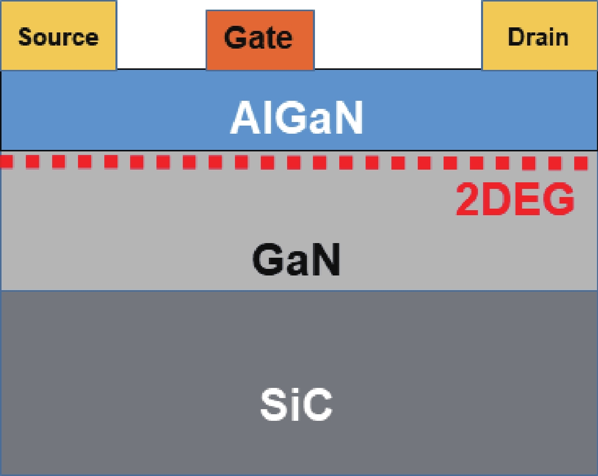
Fig. 1.
(Color online) Structure diagram of the depletion GaN HEMT.
ARTICLES
Shijie Pan1, Shiwei Feng1, , Xuan Li2, Zixuan Feng1, Xiaozhuang Lu1, Kun Bai1 and Yamin Zhang1
Corresponding author: Shiwei Feng, shwfeng@bjut.edu.cn
Abstract: In this study, the effects of 1 MeV electron radiation on the D-mode GaN-based high electron mobility transistors (HEMTs) were investigated after different radiation doses. The changes in electrical properties of the device were obtained, and the related physical mechanisms were analyzed. It indicated that under the radiation dose of 5 × 1014 cm−2, the channel current cannot be completely pinched off even if the negative gate voltage was lower than the threshold voltage, and the gate leakage current increased significantly. The emission microscopy and scanning electron microscopy were used to determine the damage location. Besides, the radiation dose was adjusted ranging from 5 × 10¹² to 1 × 1014 cm−2, and we noticed that the drain−source current increased and the threshold voltage presented slightly negative shift. By calculations, it suggested that the carrier density and electron mobility gradually increased. It provided a reference for the development of device radiation reinforcement technology.
Keywords: AlGaN/GaN HEMT, electron radiation, performance degradation, device damage
| [1] |
Bisi D, Meneghini M, de Santi C, et al. Deep-level characterization in GaN HEMTs-Part I: advantages and limitations of drain current transient measurements. IEEE Trans Electron Devices, 2013, 60(10), 3166 doi: 10.1109/TED.2013.2279021
|
| [2] |
Lu B, Palacios T. High breakdown (>1500 V) AlGaN/GaN HEMTs by substrate-transfer technology. IEEE Electron Device Lett, 2010, 31(9), 951 doi: 10.1109/LED.2010.2052587
|
| [3] |
Sabramani N K, Conuvidat J, AI Hajjar A, et al. Low-frequency drain noise characterization and TCAD physical simulations of GaN HEMTs: identification and analysis of physical location of traps. IEEE Electron Device Lett, 2018, 39(1), 107. doi: 10.1109/LED.2017.2771407
|
| [4] |
Polyakov A Y, Pearton S J, Frenzer P, et al. Radiation effects in GaN materials and devices. J Mater Chem C, 2013, 1(5), 877 doi: 10.1039/C2TC00039C
|
| [5] |
Sharma C, Visvkarma A K, Laishram R, et al. Cumulative dose γ-irradiation effects on material properties of AlGaN/GaN hetero-structures and electrical properties of HEMT devices. Semicond Sci Technol, 2019, 34(6), 65024 doi: 10.1088/1361-6641/ab11a0
|
| [6] |
Wu H, Fu X, Guo J, et al. Total ionizing dose and annealing effects on shift for p-GaN gate AlGaN/GaN HEMTs. IEEE Electron Device Lett, 2022, 43(11), 1945 doi: 10.1109/LED.2022.3205318
|
| [7] |
Tarasova E A, Obolensky S V, Galkin O E, et al. Analysis of the GaN-HEMT parameters before and after gamma-neutron irradiation. Semicond, 2017, 51(11), 1490 doi: 10.1134/S1063782617110264
|
| [8] |
Lee J, Flitsiyan E, Chernyak L, et al. Effects of gamma irradiation on AlGaN-based high electron mobility transistors. ECS J Solid State Sci Technol, 2017, 6(11), S3063 doi: 10.1149/2.0191711jss
|
| [9] |
Zheng X, Feng S, Peng C, et al. Evidence of GaN HEMT Schottky gate degradation after gamma irradiation. IEEE Trans Electron Devices, 2019, 66(9), 3784 doi: 10.1109/TED.2019.2928560
|
| [10] |
Khanal M P, Uprety S, Mirkhani V, et al. Impact of 100 keV proton irradiation on electronic and optical properties of AlGaN/GaN high electron mobility transistors (HEMTs). J Appl Phys, 2018, 124(21), 215702 doi: 10.1063/1.5054034
|
| [11] |
Lee I H, Lee C, Choi B K, et al. Proton-induced conductivity enhancement in AlGaN/GaN HEMT devices. J Korean Phys Soc, 2018, 72(8), 920 doi: 10.3938/jkps.72.920
|
| [12] |
Mcclory J W, Petrosky J C, Sattler J M, et al. An analysis of the effects of low-energy electron irradiation of AlGaN/GaN HFETs. IEEE Trans Nucl Sci, 2007, 54(6), 1946 doi: 10.1109/TNS.2007.910121
|
| [13] |
Luo Y H, Guo H X, Zhang K Y, et al. Electron beam irradiation effect on GaN HEMT. Nuclear Techniques, 2011, 34(7), 5 (in Chinese)
|
| [14] |
Liu Z L, Gao J T. Radiation effects in semiconductor materials and devices, 2020
|
| [15] |
Pearton S J, Ren F, Patrick E, et al. Review-ionizing radiation damage effects on GaN devices. ECS J Solid State Sci Technol, 2016, 5(2), Q35 doi: 10.1149/2.0251602jss
|
| [16] |
Sasaki H, Hisaka T, Kadoiwa K, et al. Ultra-high voltage electron microscopy investigation of irradiation induced displacement defects on AlGaN/GaN HEMTs. Microelectron Reliab, 2018, 81, 312 doi: 10.1016/j.microrel.2017.10.005
|
| [17] |
Oh S K, Song C G, Jang T, et al. Effect of electron-beam irradiation on leakage current of AlGaN/GaN HEMTs on sapphire. J Semicond Technol Sci, 2013, 13(6), 617 doi: 10.5573/JSTS.2013.13.6.617
|
| [18] |
Hwang Y, Liu L, Ren F, et al. Effect of electron irradiation on AlGaN/GaN and InAlN/GaN heterojunctions. J Vac Sci Technol B, 2013, 31(2), 22206 doi: 10.1116/1.4795210
|
| [19] |
Gao S, Huang Y, Zhang H, et al. Single-step electron beam evaporation for Schottky/Ohmic drain in GaN-on-Si HEMTs fabrication. IEEE Electron Device Lett, 2022, 43(12), 2049 doi: 10.1109/LED.2022.3216306
|
| [20] |
Umana Membreno G A, Dell J M, Parish G, et al. Effect of 60Co gamma-irradiation on two-dimensional electron gas transport and device characteristics of AlGaN/GaN HEMTs. phys stat sol (c), 2005, 2(7), 2581 doi: 10.1002/pssc.200461519
|
| [21] |
Jafar Rasel M A, Schoell R, AI-Mamun N S, et al. Heavy ion irradiation induced failure of gallium nitride high electron mobility transistors: effects of in-situ biasing. J Phys D: Appl Phys, 2023, 56, 305104 doi: 10.1088/1361-6463/accfa7
|
| [22] |
Zhao S L, Hou B, Chen W W, et al. Analysis of the breakdown characterization method in GaN-Based HEMTs. IEEE Trans Power Electronics, 2016, 31(2), 1517 doi: 10.1109/TPEL.2015.2416773
|
| [23] |
Wang M, Chen K J. Off-state breakdown characterization in AlGaN/GaN HEMT using drain injection technique. IEEE Trans Electron Devices, 2010, 57(7), 1492 doi: 10.1109/TED.2010.2048960
|
| [24] |
Hu X, Karmarkar A P, Jun B, et al. Proton-irradiation effects on AlGaN/AlN/GaN high electron mobility transistors. IEEE Trans Nucl Sci, 2003, 50(6), 1791 doi: 10.1109/TNS.2003.820792
|
| [25] |
Chen C, Liu X. Effects of low-energy electron irradiation on enhancement-mode AlGaN/GaN high-electron-mobility transistors. Adv Mater Res, 2013, 774, 876 doi: 10.4028/www.scientific.net/AMR.774-776.876
|
| [26] |
Vitusevich S A, Klein N, Belyaev A E, et al. Effects of γ-irradiation on AlGaN/GaN-based HEMTs. phys stat sol (a), 2003, 195(1), 101 doi: 10.1002/pssa.200306264
|
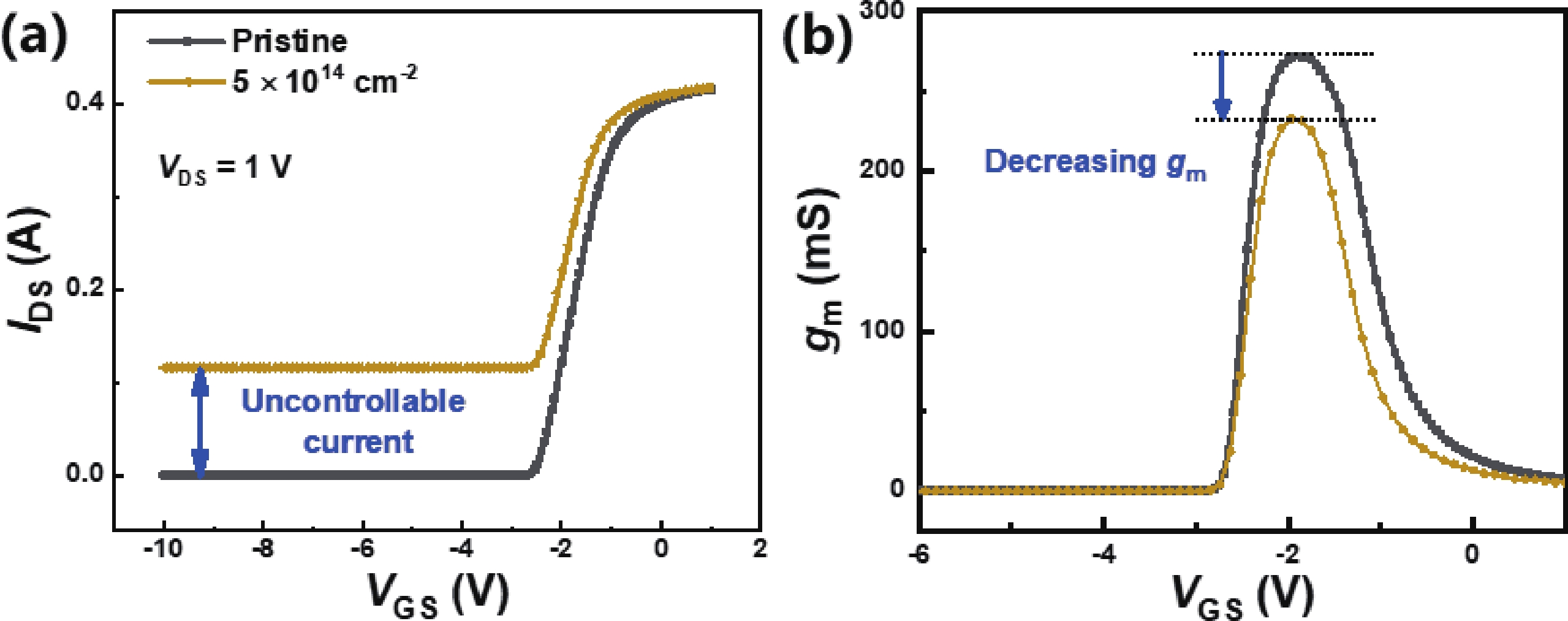
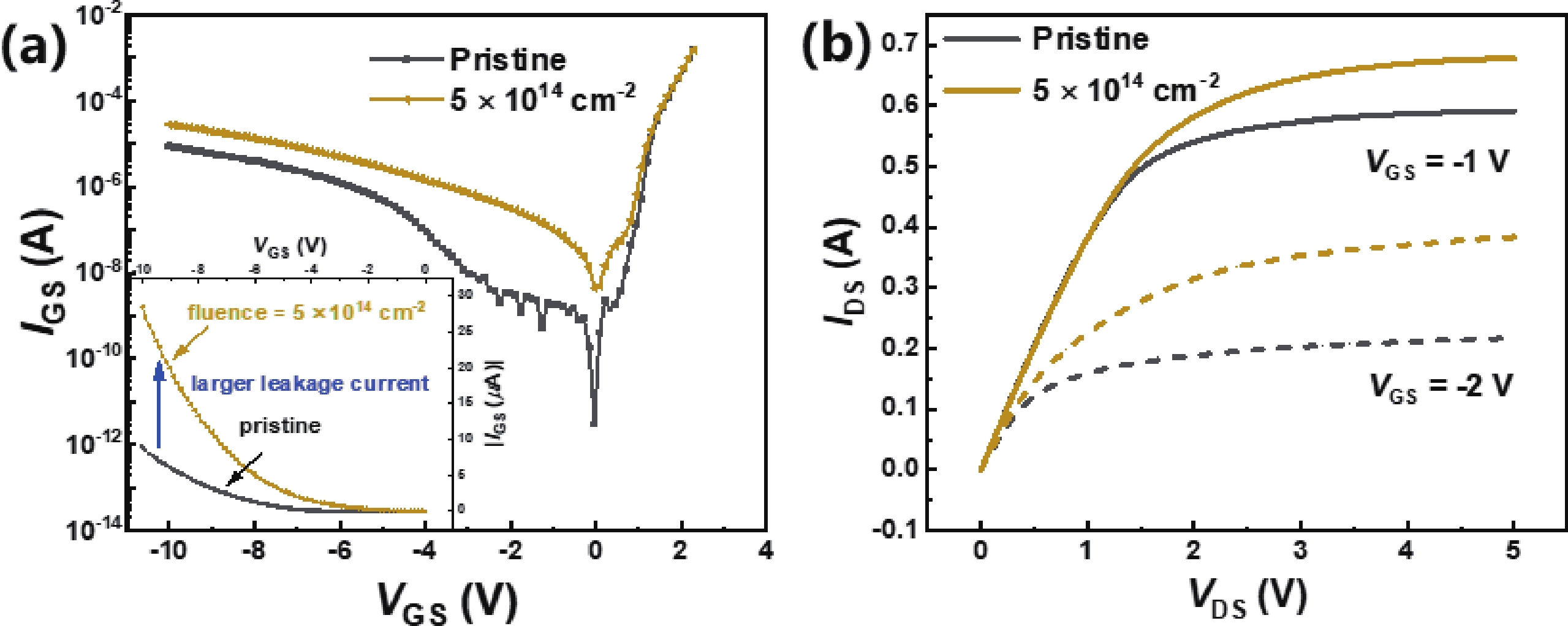
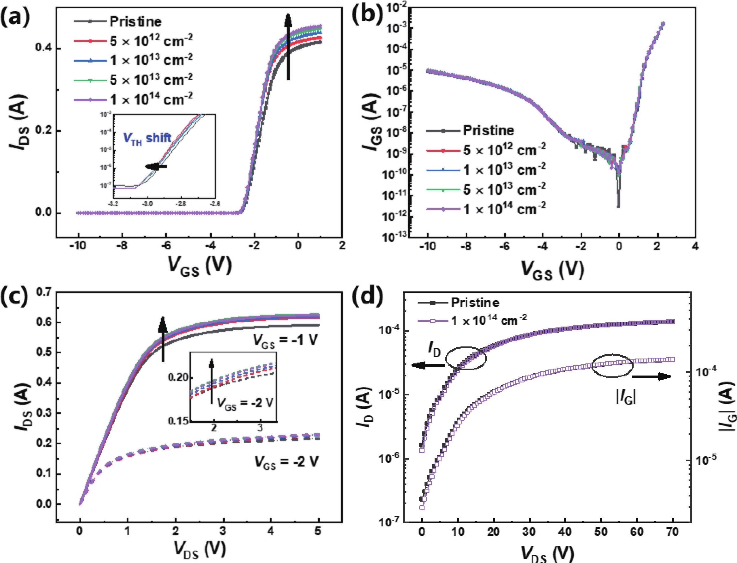
Table 1. Electrical parameters of Sample B under different radiation doses.
| Dose (cm−2) | VTH (V) | ns (1013 cm−2) | μ (cm2/(V·s)) |
| Unaged | −2.658 | 0.768 | 1194 |
| 5 × 10¹² | −2.671 | 0.772 | 1235 |
| 1 × 10¹³ | −2.682 | 0.775 | 1262 |
| 5 × 10¹³ | −2.693 | 0.778 | 1269 |
| 1 × 10¹⁴ | −2.705 | 0.782 | 1278 |
 DownLoad: CSV
| [1] |
Bisi D, Meneghini M, de Santi C, et al. Deep-level characterization in GaN HEMTs-Part I: advantages and limitations of drain current transient measurements. IEEE Trans Electron Devices, 2013, 60(10), 3166 doi: 10.1109/TED.2013.2279021
|
| [2] |
Lu B, Palacios T. High breakdown (>1500 V) AlGaN/GaN HEMTs by substrate-transfer technology. IEEE Electron Device Lett, 2010, 31(9), 951 doi: 10.1109/LED.2010.2052587
|
| [3] |
Sabramani N K, Conuvidat J, AI Hajjar A, et al. Low-frequency drain noise characterization and TCAD physical simulations of GaN HEMTs: identification and analysis of physical location of traps. IEEE Electron Device Lett, 2018, 39(1), 107. doi: 10.1109/LED.2017.2771407
|
| [4] |
Polyakov A Y, Pearton S J, Frenzer P, et al. Radiation effects in GaN materials and devices. J Mater Chem C, 2013, 1(5), 877 doi: 10.1039/C2TC00039C
|
| [5] |
Sharma C, Visvkarma A K, Laishram R, et al. Cumulative dose γ-irradiation effects on material properties of AlGaN/GaN hetero-structures and electrical properties of HEMT devices. Semicond Sci Technol, 2019, 34(6), 65024 doi: 10.1088/1361-6641/ab11a0
|
| [6] |
Wu H, Fu X, Guo J, et al. Total ionizing dose and annealing effects on shift for p-GaN gate AlGaN/GaN HEMTs. IEEE Electron Device Lett, 2022, 43(11), 1945 doi: 10.1109/LED.2022.3205318
|
| [7] |
Tarasova E A, Obolensky S V, Galkin O E, et al. Analysis of the GaN-HEMT parameters before and after gamma-neutron irradiation. Semicond, 2017, 51(11), 1490 doi: 10.1134/S1063782617110264
|
| [8] |
Lee J, Flitsiyan E, Chernyak L, et al. Effects of gamma irradiation on AlGaN-based high electron mobility transistors. ECS J Solid State Sci Technol, 2017, 6(11), S3063 doi: 10.1149/2.0191711jss
|
| [9] |
Zheng X, Feng S, Peng C, et al. Evidence of GaN HEMT Schottky gate degradation after gamma irradiation. IEEE Trans Electron Devices, 2019, 66(9), 3784 doi: 10.1109/TED.2019.2928560
|
| [10] |
Khanal M P, Uprety S, Mirkhani V, et al. Impact of 100 keV proton irradiation on electronic and optical properties of AlGaN/GaN high electron mobility transistors (HEMTs). J Appl Phys, 2018, 124(21), 215702 doi: 10.1063/1.5054034
|
| [11] |
Lee I H, Lee C, Choi B K, et al. Proton-induced conductivity enhancement in AlGaN/GaN HEMT devices. J Korean Phys Soc, 2018, 72(8), 920 doi: 10.3938/jkps.72.920
|
| [12] |
Mcclory J W, Petrosky J C, Sattler J M, et al. An analysis of the effects of low-energy electron irradiation of AlGaN/GaN HFETs. IEEE Trans Nucl Sci, 2007, 54(6), 1946 doi: 10.1109/TNS.2007.910121
|
| [13] |
Luo Y H, Guo H X, Zhang K Y, et al. Electron beam irradiation effect on GaN HEMT. Nuclear Techniques, 2011, 34(7), 5 (in Chinese)
|
| [14] |
Liu Z L, Gao J T. Radiation effects in semiconductor materials and devices, 2020
|
| [15] |
Pearton S J, Ren F, Patrick E, et al. Review-ionizing radiation damage effects on GaN devices. ECS J Solid State Sci Technol, 2016, 5(2), Q35 doi: 10.1149/2.0251602jss
|
| [16] |
Sasaki H, Hisaka T, Kadoiwa K, et al. Ultra-high voltage electron microscopy investigation of irradiation induced displacement defects on AlGaN/GaN HEMTs. Microelectron Reliab, 2018, 81, 312 doi: 10.1016/j.microrel.2017.10.005
|
| [17] |
Oh S K, Song C G, Jang T, et al. Effect of electron-beam irradiation on leakage current of AlGaN/GaN HEMTs on sapphire. J Semicond Technol Sci, 2013, 13(6), 617 doi: 10.5573/JSTS.2013.13.6.617
|
| [18] |
Hwang Y, Liu L, Ren F, et al. Effect of electron irradiation on AlGaN/GaN and InAlN/GaN heterojunctions. J Vac Sci Technol B, 2013, 31(2), 22206 doi: 10.1116/1.4795210
|
| [19] |
Gao S, Huang Y, Zhang H, et al. Single-step electron beam evaporation for Schottky/Ohmic drain in GaN-on-Si HEMTs fabrication. IEEE Electron Device Lett, 2022, 43(12), 2049 doi: 10.1109/LED.2022.3216306
|
| [20] |
Umana Membreno G A, Dell J M, Parish G, et al. Effect of 60Co gamma-irradiation on two-dimensional electron gas transport and device characteristics of AlGaN/GaN HEMTs. phys stat sol (c), 2005, 2(7), 2581 doi: 10.1002/pssc.200461519
|
| [21] |
Jafar Rasel M A, Schoell R, AI-Mamun N S, et al. Heavy ion irradiation induced failure of gallium nitride high electron mobility transistors: effects of in-situ biasing. J Phys D: Appl Phys, 2023, 56, 305104 doi: 10.1088/1361-6463/accfa7
|
| [22] |
Zhao S L, Hou B, Chen W W, et al. Analysis of the breakdown characterization method in GaN-Based HEMTs. IEEE Trans Power Electronics, 2016, 31(2), 1517 doi: 10.1109/TPEL.2015.2416773
|
| [23] |
Wang M, Chen K J. Off-state breakdown characterization in AlGaN/GaN HEMT using drain injection technique. IEEE Trans Electron Devices, 2010, 57(7), 1492 doi: 10.1109/TED.2010.2048960
|
| [24] |
Hu X, Karmarkar A P, Jun B, et al. Proton-irradiation effects on AlGaN/AlN/GaN high electron mobility transistors. IEEE Trans Nucl Sci, 2003, 50(6), 1791 doi: 10.1109/TNS.2003.820792
|
| [25] |
Chen C, Liu X. Effects of low-energy electron irradiation on enhancement-mode AlGaN/GaN high-electron-mobility transistors. Adv Mater Res, 2013, 774, 876 doi: 10.4028/www.scientific.net/AMR.774-776.876
|
| [26] |
Vitusevich S A, Klein N, Belyaev A E, et al. Effects of γ-irradiation on AlGaN/GaN-based HEMTs. phys stat sol (a), 2003, 195(1), 101 doi: 10.1002/pssa.200306264
|


Article views: 2254 Times PDF downloads: 104 Times Cited by: 0 Times
Received: 21 February 2024 Revised: 15 May 2024 Online: Accepted Manuscript: 04 June 2024Uncorrected proof: 06 June 2024Published: 15 September 2024
| Citation: |
Shijie Pan, Shiwei Feng, Xuan Li, Zixuan Feng, Xiaozhuang Lu, Kun Bai, Yamin Zhang. Effects of 1 MeV electron radiation on the AlGaN/GaN high electron mobility transistors[J]. Journal of Semiconductors, 2024, 45(9): 092503. doi: 10.1088/1674-4926/24020020
****
S J Pan, S W Feng, X Li, Z X Feng, X Z Lu, K Bai, and Y M Zhang, Effects of 1 MeV electron radiation on the AlGaN/GaN high electron mobility transistors[J]. J. Semicond., 2024, 45(9), 092503 doi: 10.1088/1674-4926/24020020

|
 Shijie Pan received the B.S. degree in electronic science and technology from the Beijing University of Technology, Beijing, China, in 2018, where she is currently pursuing the Ph.D. degree in electronic science and technology with the Laboratory of Semiconductor Device Reliability Physics. Her current research interests include the reliability of gallium nitride devices
 Shiwei Feng received the B.S. and M.S. degrees from Jilin University, Changchun, China, in 1983 and 1986, respectively, and the Ph.D. degree from Beijing University of Technology, Beijing, China, in 1999. He was a Post-Doctoral Researcher with Howard University, Washington, DC, USA, in 2000, and with Rutgers University, Newark, NJ, USA, from 2001 to 2002. In 1986, he joined the Beijing University of Technology where he is currently a Professor with the Faculty of Information Technology. His current research interests include reliability physics of semiconductor devices and thermal management of semiconductor devices
| [1] |
Bisi D, Meneghini M, de Santi C, et al. Deep-level characterization in GaN HEMTs-Part I: advantages and limitations of drain current transient measurements. IEEE Trans Electron Devices, 2013, 60(10), 3166 doi: 10.1109/TED.2013.2279021
|
| [2] |
Lu B, Palacios T. High breakdown (>1500 V) AlGaN/GaN HEMTs by substrate-transfer technology. IEEE Electron Device Lett, 2010, 31(9), 951 doi: 10.1109/LED.2010.2052587
|
| [3] |
Sabramani N K, Conuvidat J, AI Hajjar A, et al. Low-frequency drain noise characterization and TCAD physical simulations of GaN HEMTs: identification and analysis of physical location of traps. IEEE Electron Device Lett, 2018, 39(1), 107. doi: 10.1109/LED.2017.2771407
|
| [4] |
Polyakov A Y, Pearton S J, Frenzer P, et al. Radiation effects in GaN materials and devices. J Mater Chem C, 2013, 1(5), 877 doi: 10.1039/C2TC00039C
|
| [5] |
Sharma C, Visvkarma A K, Laishram R, et al. Cumulative dose γ-irradiation effects on material properties of AlGaN/GaN hetero-structures and electrical properties of HEMT devices. Semicond Sci Technol, 2019, 34(6), 65024 doi: 10.1088/1361-6641/ab11a0
|
| [6] |
Wu H, Fu X, Guo J, et al. Total ionizing dose and annealing effects on shift for p-GaN gate AlGaN/GaN HEMTs. IEEE Electron Device Lett, 2022, 43(11), 1945 doi: 10.1109/LED.2022.3205318
|
| [7] |
Tarasova E A, Obolensky S V, Galkin O E, et al. Analysis of the GaN-HEMT parameters before and after gamma-neutron irradiation. Semicond, 2017, 51(11), 1490 doi: 10.1134/S1063782617110264
|
| [8] |
Lee J, Flitsiyan E, Chernyak L, et al. Effects of gamma irradiation on AlGaN-based high electron mobility transistors. ECS J Solid State Sci Technol, 2017, 6(11), S3063 doi: 10.1149/2.0191711jss
|
| [9] |
Zheng X, Feng S, Peng C, et al. Evidence of GaN HEMT Schottky gate degradation after gamma irradiation. IEEE Trans Electron Devices, 2019, 66(9), 3784 doi: 10.1109/TED.2019.2928560
|
| [10] |
Khanal M P, Uprety S, Mirkhani V, et al. Impact of 100 keV proton irradiation on electronic and optical properties of AlGaN/GaN high electron mobility transistors (HEMTs). J Appl Phys, 2018, 124(21), 215702 doi: 10.1063/1.5054034
|
| [11] |
Lee I H, Lee C, Choi B K, et al. Proton-induced conductivity enhancement in AlGaN/GaN HEMT devices. J Korean Phys Soc, 2018, 72(8), 920 doi: 10.3938/jkps.72.920
|
| [12] |
Mcclory J W, Petrosky J C, Sattler J M, et al. An analysis of the effects of low-energy electron irradiation of AlGaN/GaN HFETs. IEEE Trans Nucl Sci, 2007, 54(6), 1946 doi: 10.1109/TNS.2007.910121
|
| [13] |
Luo Y H, Guo H X, Zhang K Y, et al. Electron beam irradiation effect on GaN HEMT. Nuclear Techniques, 2011, 34(7), 5 (in Chinese)
|
| [14] |
Liu Z L, Gao J T. Radiation effects in semiconductor materials and devices, 2020
|
| [15] |
Pearton S J, Ren F, Patrick E, et al. Review-ionizing radiation damage effects on GaN devices. ECS J Solid State Sci Technol, 2016, 5(2), Q35 doi: 10.1149/2.0251602jss
|
| [16] |
Sasaki H, Hisaka T, Kadoiwa K, et al. Ultra-high voltage electron microscopy investigation of irradiation induced displacement defects on AlGaN/GaN HEMTs. Microelectron Reliab, 2018, 81, 312 doi: 10.1016/j.microrel.2017.10.005
|
| [17] |
Oh S K, Song C G, Jang T, et al. Effect of electron-beam irradiation on leakage current of AlGaN/GaN HEMTs on sapphire. J Semicond Technol Sci, 2013, 13(6), 617 doi: 10.5573/JSTS.2013.13.6.617
|
| [18] |
Hwang Y, Liu L, Ren F, et al. Effect of electron irradiation on AlGaN/GaN and InAlN/GaN heterojunctions. J Vac Sci Technol B, 2013, 31(2), 22206 doi: 10.1116/1.4795210
|
| [19] |
Gao S, Huang Y, Zhang H, et al. Single-step electron beam evaporation for Schottky/Ohmic drain in GaN-on-Si HEMTs fabrication. IEEE Electron Device Lett, 2022, 43(12), 2049 doi: 10.1109/LED.2022.3216306
|
| [20] |
Umana Membreno G A, Dell J M, Parish G, et al. Effect of 60Co gamma-irradiation on two-dimensional electron gas transport and device characteristics of AlGaN/GaN HEMTs. phys stat sol (c), 2005, 2(7), 2581 doi: 10.1002/pssc.200461519
|
| [21] |
Jafar Rasel M A, Schoell R, AI-Mamun N S, et al. Heavy ion irradiation induced failure of gallium nitride high electron mobility transistors: effects of in-situ biasing. J Phys D: Appl Phys, 2023, 56, 305104 doi: 10.1088/1361-6463/accfa7
|
| [22] |
Zhao S L, Hou B, Chen W W, et al. Analysis of the breakdown characterization method in GaN-Based HEMTs. IEEE Trans Power Electronics, 2016, 31(2), 1517 doi: 10.1109/TPEL.2015.2416773
|
| [23] |
Wang M, Chen K J. Off-state breakdown characterization in AlGaN/GaN HEMT using drain injection technique. IEEE Trans Electron Devices, 2010, 57(7), 1492 doi: 10.1109/TED.2010.2048960
|
| [24] |
Hu X, Karmarkar A P, Jun B, et al. Proton-irradiation effects on AlGaN/AlN/GaN high electron mobility transistors. IEEE Trans Nucl Sci, 2003, 50(6), 1791 doi: 10.1109/TNS.2003.820792
|
| [25] |
Chen C, Liu X. Effects of low-energy electron irradiation on enhancement-mode AlGaN/GaN high-electron-mobility transistors. Adv Mater Res, 2013, 774, 876 doi: 10.4028/www.scientific.net/AMR.774-776.876
|
| [26] |
Vitusevich S A, Klein N, Belyaev A E, et al. Effects of γ-irradiation on AlGaN/GaN-based HEMTs. phys stat sol (a), 2003, 195(1), 101 doi: 10.1002/pssa.200306264
|

 WeChat ID
Journal of Semiconductors © 2017 All Rights Reserved 京ICP备05085259号-2


