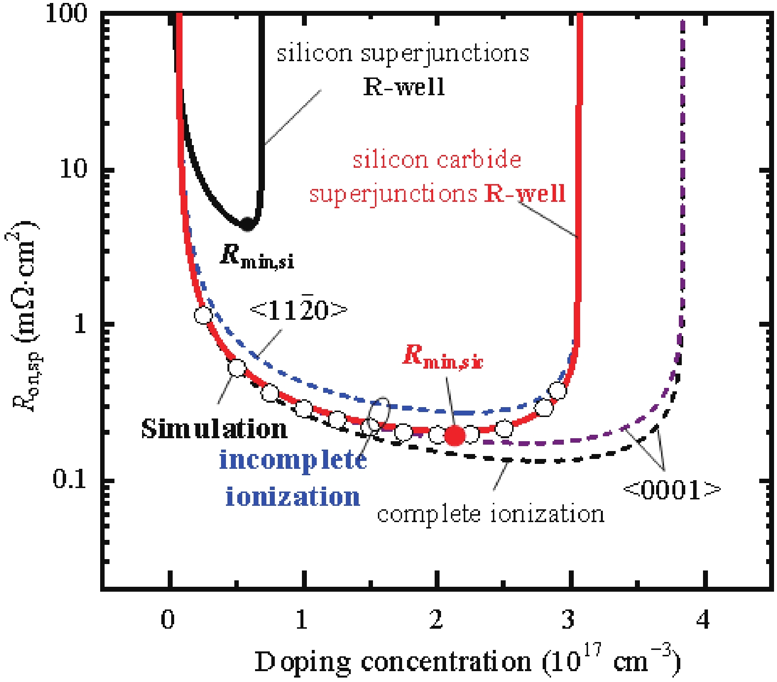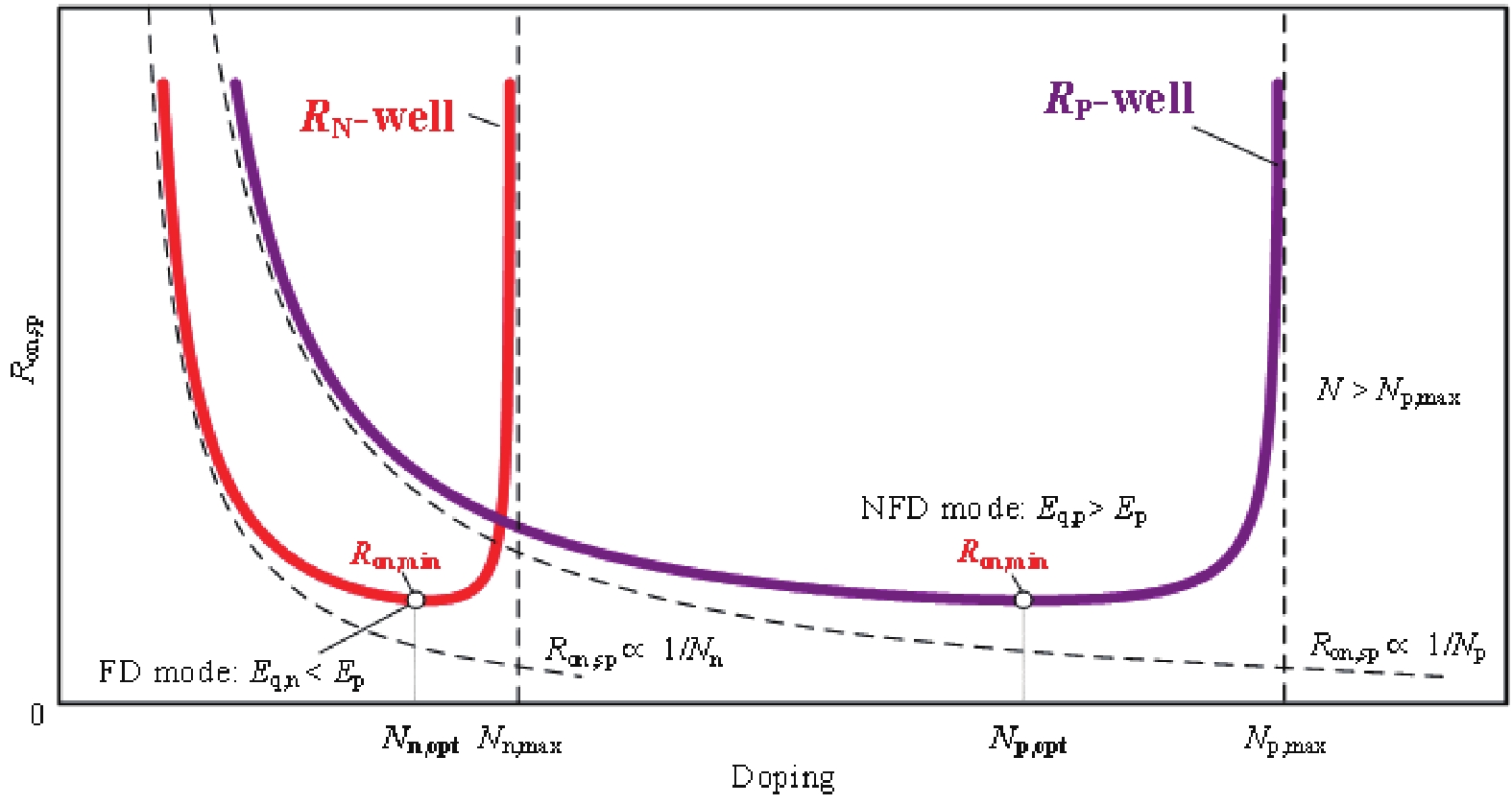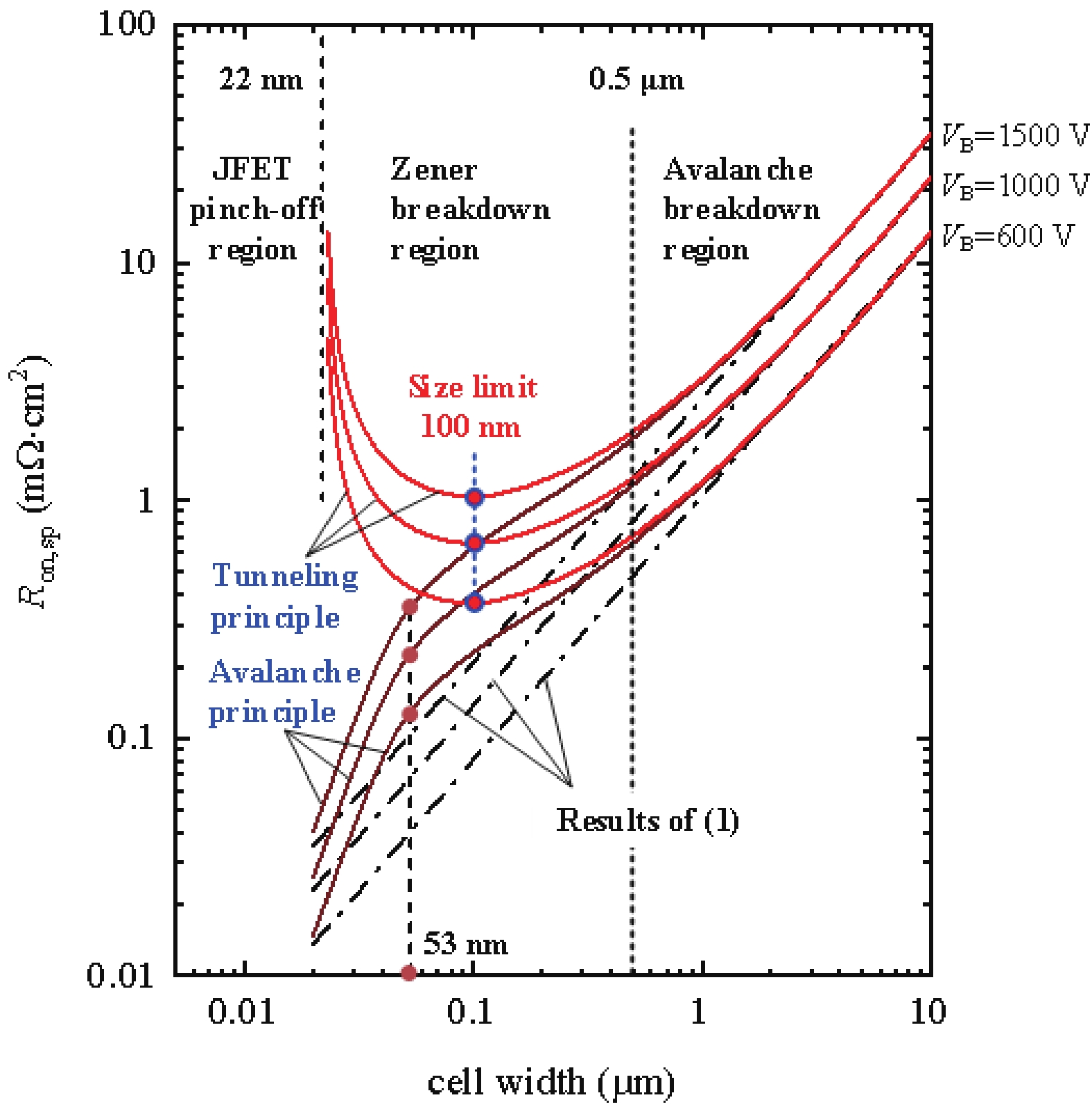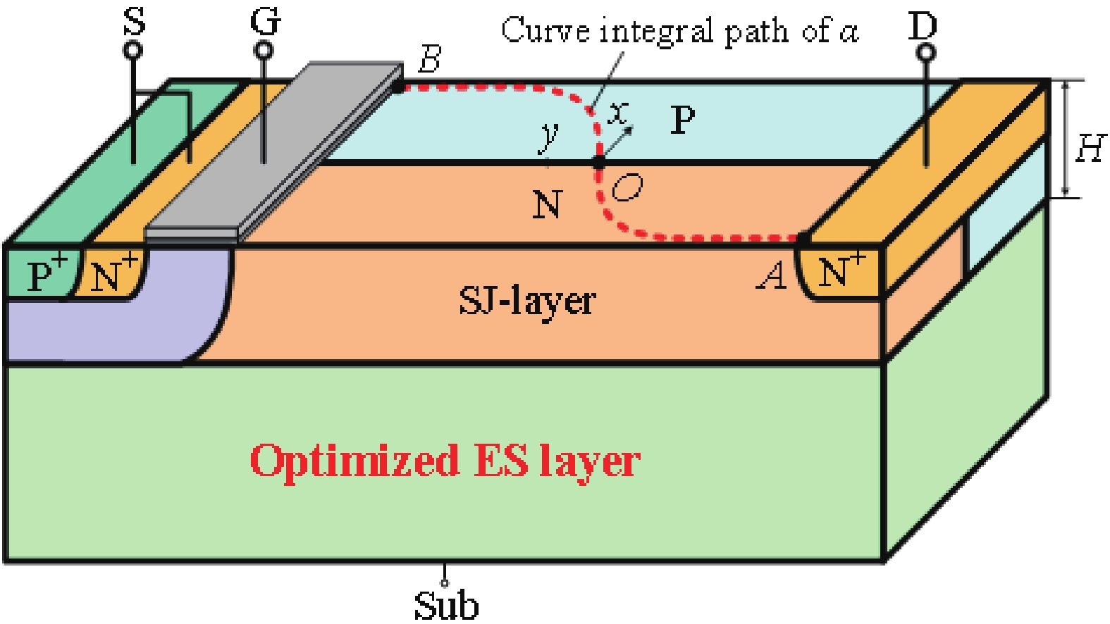
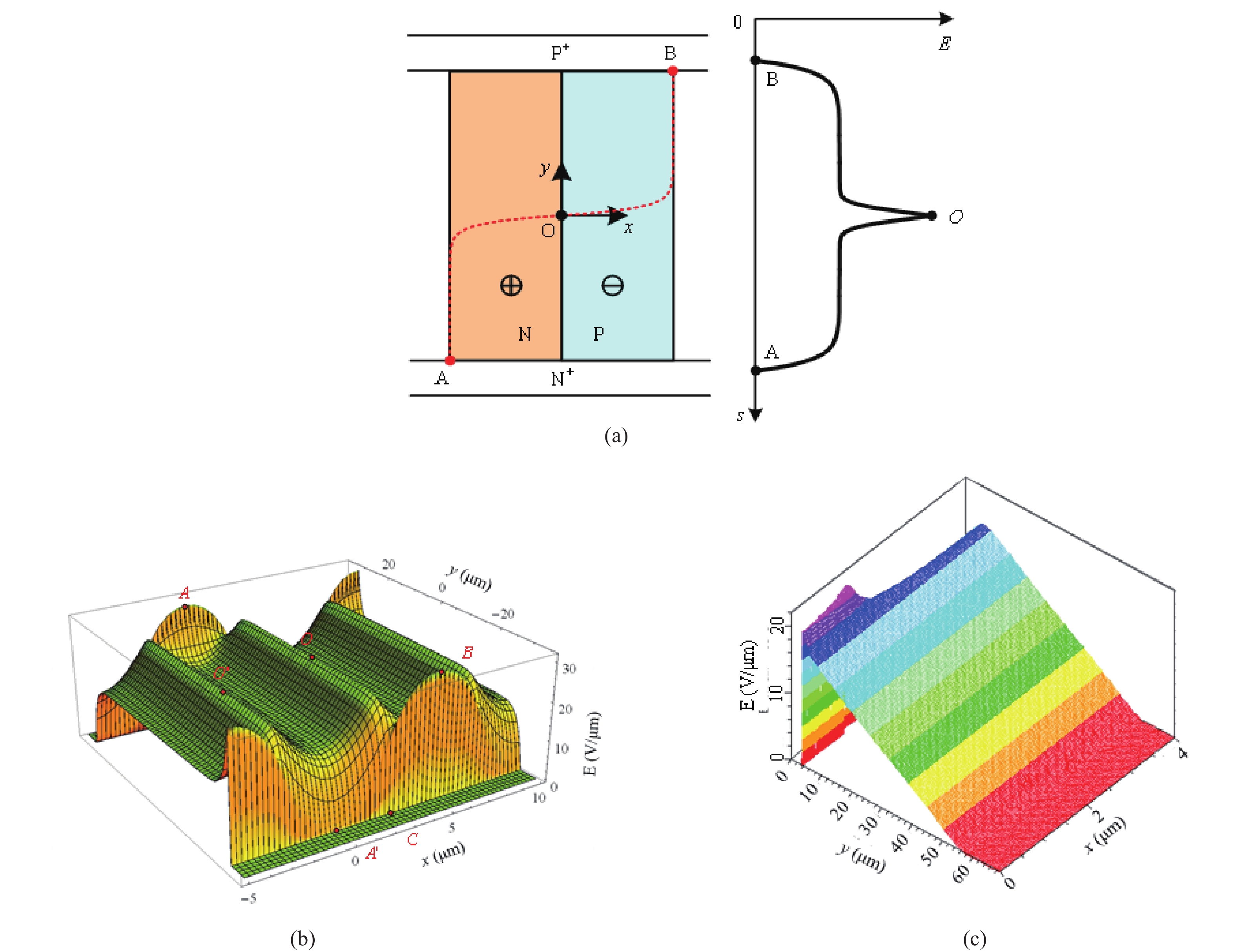
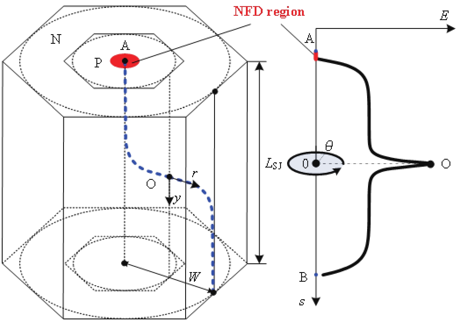
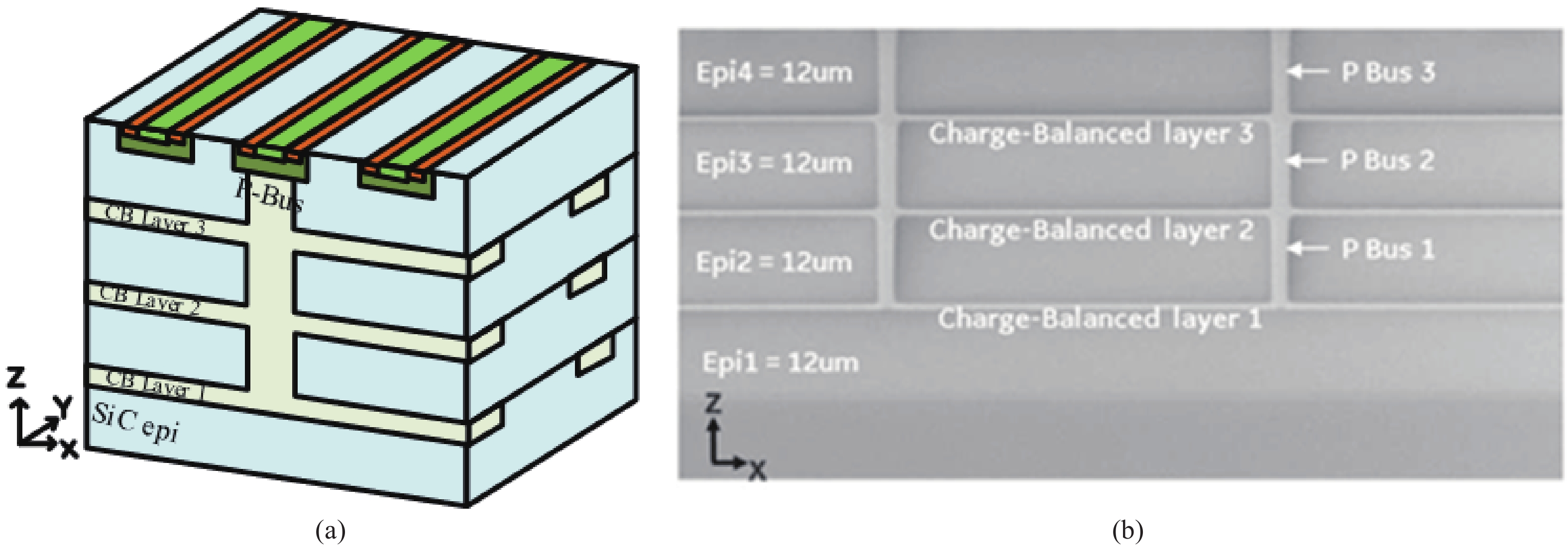
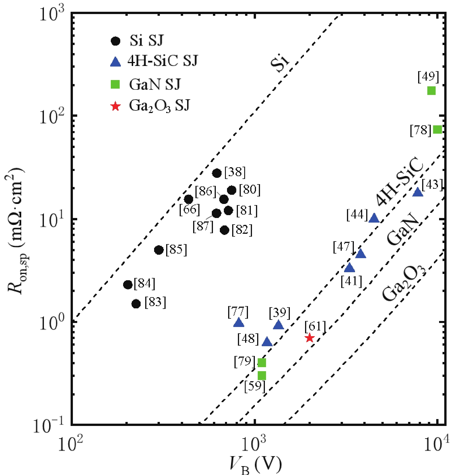
Fig. 1.
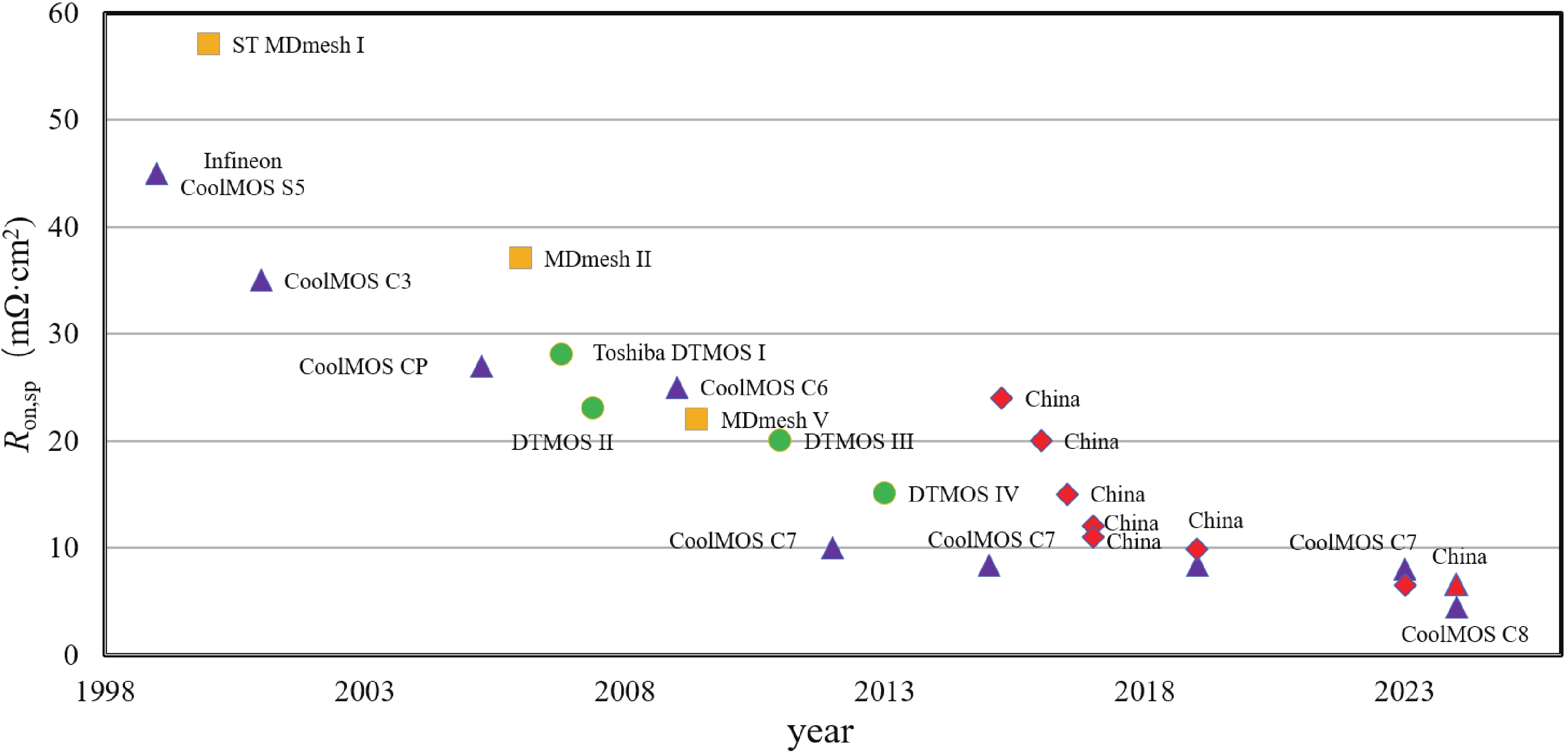
(Color online) Typical product performance of 600 V class super junction MOSFET for 25 years.
REVIEWS
Chao Ma, Weizhong Chen, Teng Liu, Wentong Zhang and Bo Zhang
Corresponding author: Bo Zhang, zhangbo@uestc.edu.cn
Abstract: Superjunction (SJ) is one of the most innovative concepts in the field of power semiconductor devices and is often referred to as a "milestone" in power MOS. Its balanced charge field modulation mechanism breaks through the strong dependency between the doping concentration in the drift region and the breakdown voltage VB in conventional devices. This results in a reduction of the trade-off relationship between specific on-resistance Ron,sp and VB from the conventional Ron,sp∝VB2.5 to Ron,sp∝W∙VB1.32, and even to Ron,sp∝W·VB1.03. As the exponential term coefficient decreases, Ron,sp decreases with the cell width W, exhibiting a development pattern reminiscent of "Moore’s Law". This paper provides an overview of the latest research developments in SJ power semiconductor devices. Firstly, it introduces the minimum specific on-resistance Ron,min theory of SJ devices, along with its combination with special effects like 3-D depletion and tunneling, discussing the development of Ron,min theory in the wide bandgap SJ field. Subsequently, it discusses the latest advancements in silicon-based and wide bandgap SJ power devices. Finally, it introduces the homogenization field (HOF) and high-K voltage-sustaining layers derived from the concept of SJ charge balance. SJ has made significant progress in device performance, reliability, and integration, and in the future, it will continue to evolve through deeper integration with different materials, processes, and packaging technologies, enhancing the overall performance of semiconductor power devices.
Keywords: super junction, silicon limit, power semiconductor device, design theory
| [1] |
Chenming H. Optimum doping profile for minimum ohmic resistance and high-breakdown voltage. IEEE Trans Electron Devices, 1979, 26(3), 243 doi: 10.1109/T-ED.1979.19416
|
| [2] |
Chen X B. Semiconductor power devices with alternating conductivity type high-voltage breakdown regions. USA Patent, US5216275, 1993
|
| [3] |
Fujihira T. Theory of Semiconductor Superjunction Devices. Jpn J Appl Phys, 1997, 36(10), 6254 doi: 10.1143/JJAP.36.6254
|
| [4] |
Lorenz L, Deboy G, Knapp A, et al. COOLMOS/sup TM/-a new milestone in high voltage power MOS. IEEE 11th International Symposium on Power Semiconductor Devices and ICs, 1999, 3 doi: 10.1109/ISPSD.1999.764028
|
| [5] |
Shenoy P M, Bhalla A, Dolny G M. Analysis of the effect of charge imbalance on the static and dynamic characteristics of the super junction MOSFET. IEEE 11th International Symposium on Power Semiconductor Devices and ICs, 1999, 99 doi: 10.1109/ISPSD.1999.764069
|
| [6] |
Chen X B, Mawby P A, K Board , et al. Theory of a novel voltage-sustaining layer for power devices. Microelectronics J, 1998, 29(12), 1005 doi: 10.1016/S0026-2692(98)00065-2
|
| [7] |
Strollo A G M, Napoli E. Optimal ON-resistance versus breakdown voltage tradeoff in superjunction power devices: a novel analytical model. IEEE Trans Electron Devices, 2001, 48(9), 2161 doi: 10.1109/16.944211
|
| [8] |
Zhang W T, Zhang B, Qiao M, et al. Optimization and new structure of super junction with isolator layer. IEEE Trans Electron Devices, 2017, 64(1), 217 doi: 10.1109/TED.2016.2628056
|
| [9] |
Zhang W T, Zhang B, Qiao M, et al. The RON, min of Balanced Symmetric Vertical Super Junction Based on R-well Model. IEEE Trans Electron Devices, 2017, 64(1), 224 doi: 10.1109/TED.2016.2632113
|
| [10] |
Zhang W, Zhang K, Wu L, et al. The minimum specific on-resistance of 3-D superjunction devices. IEEE Trans Electron Devices, 2023, 70(3), 1206 doi: 10.1109/TED.2023.3238386
|
| [11] |
Kang H and Udrea F. Theory of 3-D superjunction MOSFET. IEEE Trans Electron Devices, 2019, 66(12), 5254 doi: 10.1109/TED.2019.2947332
|
| [12] |
Chen X B, Yang H, Cheng M. New "silicon limit" of power devices. Solid State Electron, 2002, 46(8), 1185 doi: 10.1016/S0038-1101(02)00010-2
|
| [13] |
Disney D, Dolny G. JFET depletion in super junction devices. 2008 20th International Symposium on Power Semiconductor Devices and IC's, 2008, 157
|
| [14] |
Chen X. Microelectronic devices. 4th ed. Beijing: Publishing House of Electronics Industry, 2018, 1, 1
|
| [15] |
Liu E K, Zhu B S, and Luo J S. Semiconductor physics. 8th ed. Beijing: Publishing House of Electronics Industry, 2023, 1, 1
|
| [16] |
Liu E K, Zhu B S, and Luo J S. Semiconductor physics. 7th ed. Beijing: Publishing House of Electronics Industry, 2017, 1, 1
|
| [17] |
Wang C, Li X, Li L, et al. Performance limit and design guideline of 4H-SiC superjunction devices considering anisotropy of impact ionization. IEEE Electron Device Lett, 2022, 43(12), 2025 doi: 10.1109/LED.2022.3212465
|
| [18] |
Yu L, Sheng K. Modeling and optimal device design for 4H-SiC super-junction devices. IEEE Trans Electron Devices, 2008, 55(8), 1961 doi: 10.1109/TED.2008.926648
|
| [19] |
Li X, Li L, Xie K, et al. Charge imbalance tolerance of 4H-SiC superjunction devices featuring breakdown path variation. IEEE Electron Device Lett, 2023, 44(7), 1044 doi: 10.1109/LED.2023.3281328
|
| [20] |
Hatakeyama T, Nishio J, Ota C, et al. Physical modeling and scaling properties of 4H-SiC power devices. 2005 International Conference On Simulation of Semiconductor Processes and Devices, 2005, 171 doi: 10.1109/SISPAD.2005.201500
|
| [21] |
Platania E, Z Chen, F Chimento, et al. A physics-based model for a SiC JFET accounting for electric-field-dependent mobility. IEEE Trans Industry Applications, 2011, 47(1), 199 doi: 10.1109/TIA.2010.2090843
|
| [22] |
He N, Zhang S, Zhu X, et al. A 0. 25μm 700V BCD technology with ultra-low specific on-resistance SJ-LDMOS. 2020 32nd International Symposium on Power Semiconductor Devices and ICs, 2020, 419 doi: 10.1109/ISPSD46842.2020.9170046
|
| [23] |
He N, Zhang S, Wang H, et al. Ultra-high voltage BCD technology integrated 1000 V 3-D split-superjunction devices. 2022 IEEE 34th International Symposium on Power Semiconductor Devices and ICs, 2022, 305 doi: 10.1109/ISPSD49238.2022.9813681
|
| [24] |
Antoniou M, Udrea F, Bauer F. The superjunction insulated gate bipolar transistor optimization and modeling. IEEE Trans Electron Devices, 2010, 57(3), 594 doi: 10.1109/TED.2009.2039260
|
| [25] |
Fujishima N, Yano Y, Tada G, et al. N-ch IGBT with high reverse blocking capability for multipoint differential line drivers. IEEE 3rd International Symposium on Power Semiconductor Devices and ICs, 1991, 70 doi: 10.1109/ISPSD.1991.146069
|
| [26] |
Wu Y, Li Z, Pan J, et al. 650 V super-junction insulated gate bipolar transistor based on 45 μm ultrathin wafer technology. IEEE Electron Device Lett, 2022, 43(4), 592 doi: 10.1109/LED.2022.3154782
|
| [27] |
Kang H, Udrea F. Material limit of power devices—applied to asymmetric 2-D superjunction MOSFET. IEEE Trans on Electron Devices, 2018, 65(8), 3326 doi: 10.1109/TED.2018.2839180
|
| [28] |
iDEAL Semiconductor. SuperQ™ technology. https://idealsemi.com/technology/technology-1/, 2023
|
| [29] |
Nassif-khalil S G, Salama C A T. Super junction LDMOST in silicon-on-sapphire technology (SJ-LDMOST). International Symposium on Power Semiconductor Devices & IC's, 2002, 81 doi: 10.1109/ISPSD.2002.1016176
|
| [30] |
Zhang B, Zhang W T, Li Z J, et al. Equivalent substrate model for lateral super junction device. IEEE Trans Electron Devices, 2014, 61(2), 525 doi: 10.1109/TED.2013.2295091
|
| [31] |
Zhang B, Chen L, Wu J, et al. SLOP-LDMOS-a novel super-junction concept LDMOS and its experimental demonstration. International Conference on Communications, Circuits and Systems, 2005, 1402 doi: 10.1109/ICCCAS.2005.1495367
|
| [32] |
Zhang B, Wang W, Chen W, et al. High-voltage LDMOS with charge-balanced surface low on-resistance path layer. IEEE Electron Device Lett, 2009, 30(8), 849 doi: 10.1109/LED.2009.2023541
|
| [33] |
Park I Y, Salama C. CMOS compatible super junction LDMOST with n-buffer layer. International Symposium on Power Semiconductor Devices & Ics, 2005, 163 doi: 10.1109/ISPSD.2005.1487976
|
| [34] |
Zhang W T, Zhan Z Y, Yu Y, et al. Novel superjunction LDMOS (>950 V) with a thin layer SOI. IEEE Electron Device Lett, 2017, 38(11), 1555 doi: 10.1109/LED.2017.2751571
|
| [35] |
Nassif-Khalil S G, Hou Z L, Salama C A T. SJ/RESURF LDMOST. IEEE Trans Electron Devices, 2004, 51(7), 1185 doi: 10.1109/TED.2004.829876
|
| [36] |
NG R, UDREA F, SHENG K, et al. Lateral unbalanced super junction (USJ)/3D-RESURF for high breakdown voltage on SOI. International Symposium on Power Semiconductor Devices & IC's, 2001, 395 doi: 10.1109/ISPSD.2001.934637
|
| [37] |
Guo Y, Yao J, Zhang B, et al. Variation of lateral width technique in soi high-voltage lateral double-diffused metal–oxide–semiconductor transistors using high-K dielectric. IEEE Electron Device Lett, 2015, 36(3), 262 doi: 10.1109/LED.2015.2393913
|
| [38] |
Zhang W, Tian F, Liu Y, et al. Experiments of sub-micron superjunction devices with ultra-low specific on-resistance. IEEE Electron Device Lett, 2023, 44(7), 1160 doi: 10.1109/LED.2023.3274514
|
| [39] |
Zhong X, Wang B, Wang J, et al. Experimental demonstration and analysis of a 1.35-kV 0.92·mΩ∙cm2 SiC superjunction schottky diode. IEEE Trans Electron Devices, 2018, 65(4), 1458 doi: 10.1109/TED.2018.2809475
|
| [40] |
Harada S, Kobayashi Y, Kyogoku S, et al. First demonstration of dynamic characteristics for SiC superjunction MOSFET realized using multi-epitaxial growth method. International Electron Devices Meeting, 2018, 821 doi: 10.1109/IEDM.2018.8614670
|
| [41] |
Baba M, Tawara T, Morimoto T, et al. Ultra-low specific on-resistance achieved in 3.3 kV-class SiC superjunction MOSFET. International Symposium on Power Semiconductor Devices and ICs, 2021, 83 doi: 10.23919/ISPSD50666.2021.9452273
|
| [42] |
Ghandi R, Hitchcock C, Kennerly S, et al. Demonstration of 3.5kV SiC deep-implanted superjunction didoes. 2023 35th International Symposium on Power Semiconductor Devices and ICs, 2023, 13 doi: 10.1109/ISPSD57135.2023.10147432
|
| [43] |
Kosugi R, Ji S, Mochizuki K, et al. Breaking the theoretical limit of 6.5 kV-Class 4H-SiC super-junction (SJ) MOSFETs by trench-filling epitaxial growth. International Symposium on Power Semiconductor Devices and ICs, 2019, 39 doi: 10.1109/ISPSD.2019.8757632
|
| [44] |
Knoll J, Shawky M, Yen S H, et al. Characterization of 4.5 kV charge-balanced SiC MOSFETs. 2021 IEEE Applied Power Electronics Conference and Exposition, 2021, 2217 doi: 10.1109/APEC42165.2021.9487454
|
| [45] |
Ghandi R, Bolotnikov A, Lilienfeld D, et al. 3kV SiC charge-balanced diodes breaking unipolar limit. 2019 31st International Symposium on Power Semiconductor Devices and ICs, 2019, 179 doi: 10.1109/ISPSD.2019.8757568
|
| [46] |
Ghandi R, Bolotnikov A, Kennerly S, et al. 4.5kV SiC charge-balanced MOSFETs with ultra-low on-resistance. 2020 32nd International Symposium on Power Semiconductor Devices and ICs, 2020, 126 doi: 10.1109/ISPSD46842.2020.9170171
|
| [47] |
Ghandi R, Hitchcock C, Kennerly S, et al. Scalable ultrahigh voltage SiC superjunction device technologies for power electronics applications. 2022 International Electron Devices Meeting, 2022, 911 doi: 10.1109/IEDM45625.2022.10019368
|
| [48] |
Masuda T, Saito Y, Kumazawa T, et al. 0.63 mΩ·cm2/1170 V 4H-SiC super junction V-groove trench MOSFET. 2018 IEEE International Electron Devices Meeting, 2018, 811 doi: 10.1109/IEDM.2018.8614610
|
| [49] |
Ishida H, Shibata D, Matsuo H, et al. GaN-based natural super junction diodes with multi-channel structures. IEEE International Electron Devices Meeting, 2018, 1 doi: 10.1109/IEDM.2008.4796636
|
| [50] |
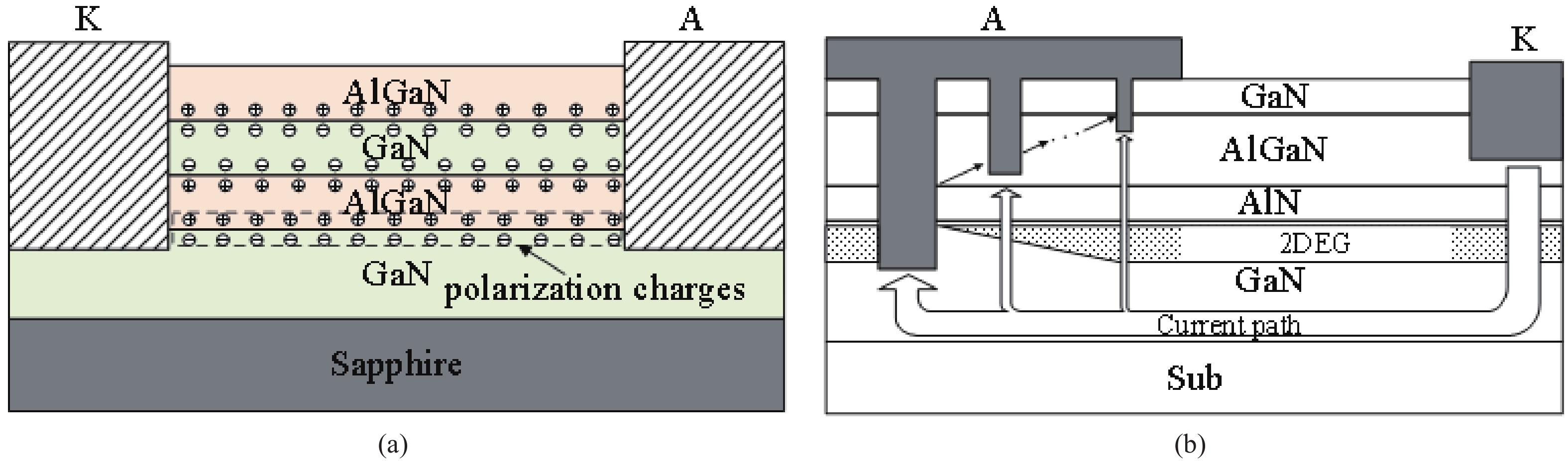
Nakajima A, Sumida Y, Dhyani M H, et al. GaN-based super heterojunction field effect transistors using the polarization junction concept. IEEE Electron Device Lett, 2011, 32(4), 542 doi: 10.1109/LED.2011.2105242
|
| [51] |
Li Z, Chow T P. Design and simulation of 5–20-kV GaN enhancement-mode vertical superjunction HEMT. IEEE Transactions on Electron Devices, 2013, 60(10), 3230 doi: 10.1109/TED.2013.2266544
|
| [52] |
Inni V, Hong L, SWEET M, et al. 2.4kV GaN polarization superjunction schottky barrier diodes on semi-insulating 6H-SiC substrate. IEEE International Symposium on Power Semiconductor Devices & IC's, 2014, 245 doi: 10.1109/ISPSD.2014.6856022
|
| [53] |
Hahn H, Reuters B, Geipel S, et al. Charge balancing in GaN-based 2-D electron gas devices employing an additional 2-D hole gas and its influence on dynamic behaviour of GaN-based heterostructure field effect transistors. J Appl Phys, 2015, 117(10), 151 doi: 10.1063/1.4913857
|
| [54] |
Napoli E. Superjunction. Wiley encyclopedia of electrical and electronics engineering. John Wiley: Sons, 2014
|
| [55] |
Shankar B, Soni A, Gupta S D, et al. Safe operating area (SOA) reliability of polarization super junction (PSJ) GaN FETs. IEEE International Reliability Physics Symposium, 2018, 1 doi: 10.1109/IRPS.2018.8353595
|
| [56] |
Zhang A, Qi Z, Chao Y, et al. Novel AlGaN/GaN SBDs with nanoscale multi-channel for gradient 2DEG modulation. 2018 IEEE 30th International Symposium on Power Semiconductor Devices and ICs, 2018, 204 doi: 10.1109/ISPSD.2018.8393638
|
| [57] |
Han S, Song J, Sadek M, et al. 12.5 kV GaN super-heterojunction schottky barrier diodes. IEEE Trans Electron Devices, 2021, 68(11), 5736 doi: 10.1109/TED.2021.3111543
|
| [58] |
Li Z, Naik H, Chow T P. Design of GaN and SiC 5–20kV vertical superjunction structures. Lester Eastman Conference on High Performance Devices, 2012, 1 doi: 10.1109/lec.2012.6410985
|
| [59] |
Zhang M, Guo Z, Huang Y, et al. Study of AlGaN/GaN vertical superjunction HEMT for improvement of breakdown voltage and specific on-resistance. IEEE Access, 2021, PP(99), 9895 doi: 10.1109/ACCESS.2021.3049374
|
| [60] |
Xiao M, Ma Y, Du Z, et al. First demonstration of vertical superjunction diode in GaN. 2022 International Electron Devices Meeting, 2022, 35.6.1 doi: 10.1109/IEDM45625.2022.10019405
|
| [61] |
Qin Y, Porter M, Xiao M, et al. 2 kV, 0.7 mΩ·cm2 vertical Ga2O3 superjunction schottky rectifier with dynamic robustness. 2023 International Electron Devices Meeting (IEDM), 2023, 1
|
| [62] |
Zhang B, Zhang W, Zu J, et al. Novel homogenization field technology in lateral power devices. IEEE Electron Device Lett, 2020, 41(11), 1677 doi: 10.1109/LED.2020.3023688
|
| [63] |
Zhang W T, Li Z J, Zhang B. A new type of homogenization field power semiconductor devices. 2022 IEEE 16th International Conference on Solid-State & Integrated Circuit Technology, 2022, 1 doi: 10.1109/ICSICT55466.2022.9963179
|
| [64] |
Zhang G, Zhang W, He J, et al. Experiments of a novel low on-resistance LDMOS with 3-D floating vertical field plate. 2019 31st International Symposium on Power Semiconductor Devices and ICs, 2019, 507 doi: 10.1109/ISPSD.2019.8757659
|
| [65] |
Zhang W, Wu Y, Zhang K, et al. Experiments of a lateral power device with complementary homogenization field structure. IEEE Electron Device Lett, 2021, 42(11), 1638 doi: 10.1109/LED.2021.3115134
|
| [66] |
Zhang W, He J, Wu Q, et al. A new multi-dimensional depletion concept of homogenization field devices. IEEE Electron Device Lett, 2023, 44(10), 1708 doi: 10.1109/LED.2023.3309917
|
| [67] |
Zhang W, Zu J, Zhu X, et al. Mechanism and experiments of a novel dielectric termination technology based on equal-potential principle. 32nd International Symposium on Power Semiconductor Devices and ICs, 2020, 38 doi: 10.1109/ISPSD46842.2020.9170124
|
| [68] |
Chen X B. Super-junction voltage sustaining layer with alternating semiconductor and high-K dielectric regions. USA Patent, US7230310, 2007
|
| [69] |
Chen X B, Huang M. A vertical power MOSFET with an interdigitated drift region using high-K insulator. IEEE Trans Electron Devices, 2012, 59(9), 2430 doi: 10.1109/TED.2012.2204890
|
| [70] |
Lyu X, Chen X. Vertical power high-K MOSFET of hexagonal layout. IEEE Trans Electron Devices, 2013, 60(5), 1709 doi: 10.1109/TED.2013.2249068
|
| [71] |
Luo X R, Cai J Y, Fan Y, et al. Novel low-resistance current path UMOS with high-K dielectric pillars. IEEE Trans Electron Devices, 2013, 60(9), 2840 doi: 10.1109/TED.2013.2272086
|
| [72] |
Chen W, Cheng, Chen X B. A novel IGBT with high-K dielectric modulation achieving ultralow turn-off loss. IEEE Trans Electron Devices, 2020, 67(3), 1066 doi: 10.1109/TED.2020.2964879
|
| [73] |
Deng J, Cheng J, Chen X B. An improved SOI p-channel LDMOS with high-K gate dielectric and dual hole-conductive paths. IEEE Electron Device Lett, 2017, 38(12), 1712 doi: 10.1109/LED.2017.2768159
|
| [74] |
Luo X, Lv M, Yin C, et al. Ultralow on-resistance SOI LDMOS with three separated gates and high-K dielectric. IEEE Trans Electron Devices, 2016, 63(9), 3804 doi: 10.1109/TED.2016.2589322
|
| [75] |
Cao Z, Duan B, Song H, et al. Novel superjunction LDMOS with a high-K dielectric trench by TCAD simulation study. IEEE Trans Electron Devices, 2019, 66(5), 2327 doi: 10.1109/TED.2019.2906911
|
| [76] |
Cheng J, Chen W, Lin J, et al. Potential of utilizing high-K film to improve the cost performance of trench LDMOS. IEEE Trans Electron Devices, 2019, 66(7), 3049 doi: 10.1109/TED.2019.2913780
|
| [77] |
Masuda T, Kosugi R, Hiyoshi T. 0.97 mΩ·cm2/820 V 4H-SiC super junction V-groove trench MOSFET. 2016 European Conference on Silicon Carbide & Related Materials, 2016, 1 doi: 10.4028/www.scientific.net/MSF.897.483
|
| [78] |
Kemmerling J, Guan R, Sadek M, et al. GaN super-heterojunction FETs with 10-kV blocking and 3-kV dynamic switching. IEEE Trans Electron Devices, 2024, 71(2), 1153 doi: 10.1109/TED.2023.3346356
|
| [79] |
Ma Y, Poter M, Qin Y, et al. 1 kV self-aligned vertical GaN superjunction diode. IEEE Electron Device Lett, 2024, 45(1), 12 doi: 10.1109/LED.2023.3332855
|
| [80] |
Qin Y, Poter M, Xiao M, et al. 2 kV, 0.7 mΩ·cm2 vertical Ga2O3 superjunction schottky rectifier with dynamic robustness. 2023 International Electron Devices Meeting, 2023, 1 doi: 10.1109/IEDM45741.2023.10413795
|
| [81] |
Lee S, Oh K, Kim S, et al. 650V superjunction MOSFET using universal charge balance concept through drift region. 2014 IEEE 26th International Symposium on Power Semiconductor Devices and IC's, 2014, 83 doi: 10.1109/ISPSD.2014.6855981
|
| [82] |
Wang Y, Qiao M, Li J, et al. Optimization of reverse recovery characteristics based on termination structure for 700V super-junction VDMOS. 2023 35th International Symposium on Power Semiconductor Devices and ICs, 2023, 171 doi: 10.1109/ISPSD57135.2023.10147399
|
| [83] |
Sakakibara J, Noda Y, Shibata T, et al. 600V-class super junction MOSFET with high aspect ratio P/N columns structure. 2008 20th International Symposium on Power Semiconductor Devices and IC's, 2008, 299 doi: 10.1109/ISPSD.2008.4538958
|
| [84] |
Yamauchi S, Shibata T, Nogami S, et al. 200V super junction MOSFET fabricated by high aspect ratio trench filling. 2006 IEEE International Symposium on Power Semiconductor Devices and IC's, 2006, 1 doi: 10.1109/ISPSD.2006.1666072
|
| [85] |
Hattori Y, Nakashima K, Kuwahara M, et al. Design of a 200V super junction MOSFET with n-buffer regions and its fabrication by trench filling. IEEE International Symposium on Power Semiconductor Devices & IC's, 2004, 189 doi: 10.1109/WCT.2004.239903
|
| [86] |
Nitta T, Minato T, Yano M, et al. Experimental results and simulation analysis of 250 V super trench power MOSFET (STM). IEEE International Symposium on Power Semiconductor Devices & IC's, 2000, 77 doi: 10.1109/ISPSD.2000.856777
|
| [1] |
Chenming H. Optimum doping profile for minimum ohmic resistance and high-breakdown voltage. IEEE Trans Electron Devices, 1979, 26(3), 243 doi: 10.1109/T-ED.1979.19416
|
| [2] |
Chen X B. Semiconductor power devices with alternating conductivity type high-voltage breakdown regions. USA Patent, US5216275, 1993
|
| [3] |
Fujihira T. Theory of Semiconductor Superjunction Devices. Jpn J Appl Phys, 1997, 36(10), 6254 doi: 10.1143/JJAP.36.6254
|
| [4] |
Lorenz L, Deboy G, Knapp A, et al. COOLMOS/sup TM/-a new milestone in high voltage power MOS. IEEE 11th International Symposium on Power Semiconductor Devices and ICs, 1999, 3 doi: 10.1109/ISPSD.1999.764028
|
| [5] |
Shenoy P M, Bhalla A, Dolny G M. Analysis of the effect of charge imbalance on the static and dynamic characteristics of the super junction MOSFET. IEEE 11th International Symposium on Power Semiconductor Devices and ICs, 1999, 99 doi: 10.1109/ISPSD.1999.764069
|
| [6] |
Chen X B, Mawby P A, K Board , et al. Theory of a novel voltage-sustaining layer for power devices. Microelectronics J, 1998, 29(12), 1005 doi: 10.1016/S0026-2692(98)00065-2
|
| [7] |
Strollo A G M, Napoli E. Optimal ON-resistance versus breakdown voltage tradeoff in superjunction power devices: a novel analytical model. IEEE Trans Electron Devices, 2001, 48(9), 2161 doi: 10.1109/16.944211
|
| [8] |
Zhang W T, Zhang B, Qiao M, et al. Optimization and new structure of super junction with isolator layer. IEEE Trans Electron Devices, 2017, 64(1), 217 doi: 10.1109/TED.2016.2628056
|
| [9] |
Zhang W T, Zhang B, Qiao M, et al. The RON, min of Balanced Symmetric Vertical Super Junction Based on R-well Model. IEEE Trans Electron Devices, 2017, 64(1), 224 doi: 10.1109/TED.2016.2632113
|
| [10] |
Zhang W, Zhang K, Wu L, et al. The minimum specific on-resistance of 3-D superjunction devices. IEEE Trans Electron Devices, 2023, 70(3), 1206 doi: 10.1109/TED.2023.3238386
|
| [11] |
Kang H and Udrea F. Theory of 3-D superjunction MOSFET. IEEE Trans Electron Devices, 2019, 66(12), 5254 doi: 10.1109/TED.2019.2947332
|
| [12] |
Chen X B, Yang H, Cheng M. New "silicon limit" of power devices. Solid State Electron, 2002, 46(8), 1185 doi: 10.1016/S0038-1101(02)00010-2
|
| [13] |
Disney D, Dolny G. JFET depletion in super junction devices. 2008 20th International Symposium on Power Semiconductor Devices and IC's, 2008, 157
|
| [14] |
Chen X. Microelectronic devices. 4th ed. Beijing: Publishing House of Electronics Industry, 2018, 1, 1
|
| [15] |
Liu E K, Zhu B S, and Luo J S. Semiconductor physics. 8th ed. Beijing: Publishing House of Electronics Industry, 2023, 1, 1
|
| [16] |
Liu E K, Zhu B S, and Luo J S. Semiconductor physics. 7th ed. Beijing: Publishing House of Electronics Industry, 2017, 1, 1
|
| [17] |
Wang C, Li X, Li L, et al. Performance limit and design guideline of 4H-SiC superjunction devices considering anisotropy of impact ionization. IEEE Electron Device Lett, 2022, 43(12), 2025 doi: 10.1109/LED.2022.3212465
|
| [18] |
Yu L, Sheng K. Modeling and optimal device design for 4H-SiC super-junction devices. IEEE Trans Electron Devices, 2008, 55(8), 1961 doi: 10.1109/TED.2008.926648
|
| [19] |
Li X, Li L, Xie K, et al. Charge imbalance tolerance of 4H-SiC superjunction devices featuring breakdown path variation. IEEE Electron Device Lett, 2023, 44(7), 1044 doi: 10.1109/LED.2023.3281328
|
| [20] |
Hatakeyama T, Nishio J, Ota C, et al. Physical modeling and scaling properties of 4H-SiC power devices. 2005 International Conference On Simulation of Semiconductor Processes and Devices, 2005, 171 doi: 10.1109/SISPAD.2005.201500
|
| [21] |
Platania E, Z Chen, F Chimento, et al. A physics-based model for a SiC JFET accounting for electric-field-dependent mobility. IEEE Trans Industry Applications, 2011, 47(1), 199 doi: 10.1109/TIA.2010.2090843
|
| [22] |
He N, Zhang S, Zhu X, et al. A 0. 25μm 700V BCD technology with ultra-low specific on-resistance SJ-LDMOS. 2020 32nd International Symposium on Power Semiconductor Devices and ICs, 2020, 419 doi: 10.1109/ISPSD46842.2020.9170046
|
| [23] |
He N, Zhang S, Wang H, et al. Ultra-high voltage BCD technology integrated 1000 V 3-D split-superjunction devices. 2022 IEEE 34th International Symposium on Power Semiconductor Devices and ICs, 2022, 305 doi: 10.1109/ISPSD49238.2022.9813681
|
| [24] |
Antoniou M, Udrea F, Bauer F. The superjunction insulated gate bipolar transistor optimization and modeling. IEEE Trans Electron Devices, 2010, 57(3), 594 doi: 10.1109/TED.2009.2039260
|
| [25] |
Fujishima N, Yano Y, Tada G, et al. N-ch IGBT with high reverse blocking capability for multipoint differential line drivers. IEEE 3rd International Symposium on Power Semiconductor Devices and ICs, 1991, 70 doi: 10.1109/ISPSD.1991.146069
|
| [26] |
Wu Y, Li Z, Pan J, et al. 650 V super-junction insulated gate bipolar transistor based on 45 μm ultrathin wafer technology. IEEE Electron Device Lett, 2022, 43(4), 592 doi: 10.1109/LED.2022.3154782
|
| [27] |
Kang H, Udrea F. Material limit of power devices—applied to asymmetric 2-D superjunction MOSFET. IEEE Trans on Electron Devices, 2018, 65(8), 3326 doi: 10.1109/TED.2018.2839180
|
| [28] |
iDEAL Semiconductor. SuperQ™ technology. https://idealsemi.com/technology/technology-1/, 2023
|
| [29] |
Nassif-khalil S G, Salama C A T. Super junction LDMOST in silicon-on-sapphire technology (SJ-LDMOST). International Symposium on Power Semiconductor Devices & IC's, 2002, 81 doi: 10.1109/ISPSD.2002.1016176
|
| [30] |
Zhang B, Zhang W T, Li Z J, et al. Equivalent substrate model for lateral super junction device. IEEE Trans Electron Devices, 2014, 61(2), 525 doi: 10.1109/TED.2013.2295091
|
| [31] |
Zhang B, Chen L, Wu J, et al. SLOP-LDMOS-a novel super-junction concept LDMOS and its experimental demonstration. International Conference on Communications, Circuits and Systems, 2005, 1402 doi: 10.1109/ICCCAS.2005.1495367
|
| [32] |
Zhang B, Wang W, Chen W, et al. High-voltage LDMOS with charge-balanced surface low on-resistance path layer. IEEE Electron Device Lett, 2009, 30(8), 849 doi: 10.1109/LED.2009.2023541
|
| [33] |
Park I Y, Salama C. CMOS compatible super junction LDMOST with n-buffer layer. International Symposium on Power Semiconductor Devices & Ics, 2005, 163 doi: 10.1109/ISPSD.2005.1487976
|
| [34] |
Zhang W T, Zhan Z Y, Yu Y, et al. Novel superjunction LDMOS (>950 V) with a thin layer SOI. IEEE Electron Device Lett, 2017, 38(11), 1555 doi: 10.1109/LED.2017.2751571
|
| [35] |
Nassif-Khalil S G, Hou Z L, Salama C A T. SJ/RESURF LDMOST. IEEE Trans Electron Devices, 2004, 51(7), 1185 doi: 10.1109/TED.2004.829876
|
| [36] |
NG R, UDREA F, SHENG K, et al. Lateral unbalanced super junction (USJ)/3D-RESURF for high breakdown voltage on SOI. International Symposium on Power Semiconductor Devices & IC's, 2001, 395 doi: 10.1109/ISPSD.2001.934637
|
| [37] |
Guo Y, Yao J, Zhang B, et al. Variation of lateral width technique in soi high-voltage lateral double-diffused metal–oxide–semiconductor transistors using high-K dielectric. IEEE Electron Device Lett, 2015, 36(3), 262 doi: 10.1109/LED.2015.2393913
|
| [38] |
Zhang W, Tian F, Liu Y, et al. Experiments of sub-micron superjunction devices with ultra-low specific on-resistance. IEEE Electron Device Lett, 2023, 44(7), 1160 doi: 10.1109/LED.2023.3274514
|
| [39] |
Zhong X, Wang B, Wang J, et al. Experimental demonstration and analysis of a 1.35-kV 0.92·mΩ∙cm2 SiC superjunction schottky diode. IEEE Trans Electron Devices, 2018, 65(4), 1458 doi: 10.1109/TED.2018.2809475
|
| [40] |
Harada S, Kobayashi Y, Kyogoku S, et al. First demonstration of dynamic characteristics for SiC superjunction MOSFET realized using multi-epitaxial growth method. International Electron Devices Meeting, 2018, 821 doi: 10.1109/IEDM.2018.8614670
|
| [41] |
Baba M, Tawara T, Morimoto T, et al. Ultra-low specific on-resistance achieved in 3.3 kV-class SiC superjunction MOSFET. International Symposium on Power Semiconductor Devices and ICs, 2021, 83 doi: 10.23919/ISPSD50666.2021.9452273
|
| [42] |
Ghandi R, Hitchcock C, Kennerly S, et al. Demonstration of 3.5kV SiC deep-implanted superjunction didoes. 2023 35th International Symposium on Power Semiconductor Devices and ICs, 2023, 13 doi: 10.1109/ISPSD57135.2023.10147432
|
| [43] |
Kosugi R, Ji S, Mochizuki K, et al. Breaking the theoretical limit of 6.5 kV-Class 4H-SiC super-junction (SJ) MOSFETs by trench-filling epitaxial growth. International Symposium on Power Semiconductor Devices and ICs, 2019, 39 doi: 10.1109/ISPSD.2019.8757632
|
| [44] |
Knoll J, Shawky M, Yen S H, et al. Characterization of 4.5 kV charge-balanced SiC MOSFETs. 2021 IEEE Applied Power Electronics Conference and Exposition, 2021, 2217 doi: 10.1109/APEC42165.2021.9487454
|
| [45] |
Ghandi R, Bolotnikov A, Lilienfeld D, et al. 3kV SiC charge-balanced diodes breaking unipolar limit. 2019 31st International Symposium on Power Semiconductor Devices and ICs, 2019, 179 doi: 10.1109/ISPSD.2019.8757568
|
| [46] |
Ghandi R, Bolotnikov A, Kennerly S, et al. 4.5kV SiC charge-balanced MOSFETs with ultra-low on-resistance. 2020 32nd International Symposium on Power Semiconductor Devices and ICs, 2020, 126 doi: 10.1109/ISPSD46842.2020.9170171
|
| [47] |
Ghandi R, Hitchcock C, Kennerly S, et al. Scalable ultrahigh voltage SiC superjunction device technologies for power electronics applications. 2022 International Electron Devices Meeting, 2022, 911 doi: 10.1109/IEDM45625.2022.10019368
|
| [48] |
Masuda T, Saito Y, Kumazawa T, et al. 0.63 mΩ·cm2/1170 V 4H-SiC super junction V-groove trench MOSFET. 2018 IEEE International Electron Devices Meeting, 2018, 811 doi: 10.1109/IEDM.2018.8614610
|
| [49] |
Ishida H, Shibata D, Matsuo H, et al. GaN-based natural super junction diodes with multi-channel structures. IEEE International Electron Devices Meeting, 2018, 1 doi: 10.1109/IEDM.2008.4796636
|
| [50] |
Nakajima A, Sumida Y, Dhyani M H, et al. GaN-based super heterojunction field effect transistors using the polarization junction concept. IEEE Electron Device Lett, 2011, 32(4), 542 doi: 10.1109/LED.2011.2105242
|
| [51] |
Li Z, Chow T P. Design and simulation of 5–20-kV GaN enhancement-mode vertical superjunction HEMT. IEEE Transactions on Electron Devices, 2013, 60(10), 3230 doi: 10.1109/TED.2013.2266544
|
| [52] |
Inni V, Hong L, SWEET M, et al. 2.4kV GaN polarization superjunction schottky barrier diodes on semi-insulating 6H-SiC substrate. IEEE International Symposium on Power Semiconductor Devices & IC's, 2014, 245 doi: 10.1109/ISPSD.2014.6856022
|
| [53] |
Hahn H, Reuters B, Geipel S, et al. Charge balancing in GaN-based 2-D electron gas devices employing an additional 2-D hole gas and its influence on dynamic behaviour of GaN-based heterostructure field effect transistors. J Appl Phys, 2015, 117(10), 151 doi: 10.1063/1.4913857
|
| [54] |
Napoli E. Superjunction. Wiley encyclopedia of electrical and electronics engineering. John Wiley: Sons, 2014
|
| [55] |
Shankar B, Soni A, Gupta S D, et al. Safe operating area (SOA) reliability of polarization super junction (PSJ) GaN FETs. IEEE International Reliability Physics Symposium, 2018, 1 doi: 10.1109/IRPS.2018.8353595
|
| [56] |
Zhang A, Qi Z, Chao Y, et al. Novel AlGaN/GaN SBDs with nanoscale multi-channel for gradient 2DEG modulation. 2018 IEEE 30th International Symposium on Power Semiconductor Devices and ICs, 2018, 204 doi: 10.1109/ISPSD.2018.8393638
|
| [57] |
Han S, Song J, Sadek M, et al. 12.5 kV GaN super-heterojunction schottky barrier diodes. IEEE Trans Electron Devices, 2021, 68(11), 5736 doi: 10.1109/TED.2021.3111543
|
| [58] |
Li Z, Naik H, Chow T P. Design of GaN and SiC 5–20kV vertical superjunction structures. Lester Eastman Conference on High Performance Devices, 2012, 1 doi: 10.1109/lec.2012.6410985
|
| [59] |
Zhang M, Guo Z, Huang Y, et al. Study of AlGaN/GaN vertical superjunction HEMT for improvement of breakdown voltage and specific on-resistance. IEEE Access, 2021, PP(99), 9895 doi: 10.1109/ACCESS.2021.3049374
|
| [60] |
Xiao M, Ma Y, Du Z, et al. First demonstration of vertical superjunction diode in GaN. 2022 International Electron Devices Meeting, 2022, 35.6.1 doi: 10.1109/IEDM45625.2022.10019405
|
| [61] |
Qin Y, Porter M, Xiao M, et al. 2 kV, 0.7 mΩ·cm2 vertical Ga2O3 superjunction schottky rectifier with dynamic robustness. 2023 International Electron Devices Meeting (IEDM), 2023, 1
|
| [62] |
Zhang B, Zhang W, Zu J, et al. Novel homogenization field technology in lateral power devices. IEEE Electron Device Lett, 2020, 41(11), 1677 doi: 10.1109/LED.2020.3023688
|
| [63] |
Zhang W T, Li Z J, Zhang B. A new type of homogenization field power semiconductor devices. 2022 IEEE 16th International Conference on Solid-State & Integrated Circuit Technology, 2022, 1 doi: 10.1109/ICSICT55466.2022.9963179
|
| [64] |
Zhang G, Zhang W, He J, et al. Experiments of a novel low on-resistance LDMOS with 3-D floating vertical field plate. 2019 31st International Symposium on Power Semiconductor Devices and ICs, 2019, 507 doi: 10.1109/ISPSD.2019.8757659
|
| [65] |
Zhang W, Wu Y, Zhang K, et al. Experiments of a lateral power device with complementary homogenization field structure. IEEE Electron Device Lett, 2021, 42(11), 1638 doi: 10.1109/LED.2021.3115134
|
| [66] |
Zhang W, He J, Wu Q, et al. A new multi-dimensional depletion concept of homogenization field devices. IEEE Electron Device Lett, 2023, 44(10), 1708 doi: 10.1109/LED.2023.3309917
|
| [67] |
Zhang W, Zu J, Zhu X, et al. Mechanism and experiments of a novel dielectric termination technology based on equal-potential principle. 32nd International Symposium on Power Semiconductor Devices and ICs, 2020, 38 doi: 10.1109/ISPSD46842.2020.9170124
|
| [68] |
Chen X B. Super-junction voltage sustaining layer with alternating semiconductor and high-K dielectric regions. USA Patent, US7230310, 2007
|
| [69] |
Chen X B, Huang M. A vertical power MOSFET with an interdigitated drift region using high-K insulator. IEEE Trans Electron Devices, 2012, 59(9), 2430 doi: 10.1109/TED.2012.2204890
|
| [70] |
Lyu X, Chen X. Vertical power high-K MOSFET of hexagonal layout. IEEE Trans Electron Devices, 2013, 60(5), 1709 doi: 10.1109/TED.2013.2249068
|
| [71] |
Luo X R, Cai J Y, Fan Y, et al. Novel low-resistance current path UMOS with high-K dielectric pillars. IEEE Trans Electron Devices, 2013, 60(9), 2840 doi: 10.1109/TED.2013.2272086
|
| [72] |
Chen W, Cheng, Chen X B. A novel IGBT with high-K dielectric modulation achieving ultralow turn-off loss. IEEE Trans Electron Devices, 2020, 67(3), 1066 doi: 10.1109/TED.2020.2964879
|
| [73] |
Deng J, Cheng J, Chen X B. An improved SOI p-channel LDMOS with high-K gate dielectric and dual hole-conductive paths. IEEE Electron Device Lett, 2017, 38(12), 1712 doi: 10.1109/LED.2017.2768159
|
| [74] |
Luo X, Lv M, Yin C, et al. Ultralow on-resistance SOI LDMOS with three separated gates and high-K dielectric. IEEE Trans Electron Devices, 2016, 63(9), 3804 doi: 10.1109/TED.2016.2589322
|
| [75] |
Cao Z, Duan B, Song H, et al. Novel superjunction LDMOS with a high-K dielectric trench by TCAD simulation study. IEEE Trans Electron Devices, 2019, 66(5), 2327 doi: 10.1109/TED.2019.2906911
|
| [76] |
Cheng J, Chen W, Lin J, et al. Potential of utilizing high-K film to improve the cost performance of trench LDMOS. IEEE Trans Electron Devices, 2019, 66(7), 3049 doi: 10.1109/TED.2019.2913780
|
| [77] |
Masuda T, Kosugi R, Hiyoshi T. 0.97 mΩ·cm2/820 V 4H-SiC super junction V-groove trench MOSFET. 2016 European Conference on Silicon Carbide & Related Materials, 2016, 1 doi: 10.4028/www.scientific.net/MSF.897.483
|
| [78] |
Kemmerling J, Guan R, Sadek M, et al. GaN super-heterojunction FETs with 10-kV blocking and 3-kV dynamic switching. IEEE Trans Electron Devices, 2024, 71(2), 1153 doi: 10.1109/TED.2023.3346356
|
| [79] |
Ma Y, Poter M, Qin Y, et al. 1 kV self-aligned vertical GaN superjunction diode. IEEE Electron Device Lett, 2024, 45(1), 12 doi: 10.1109/LED.2023.3332855
|
| [80] |
Qin Y, Poter M, Xiao M, et al. 2 kV, 0.7 mΩ·cm2 vertical Ga2O3 superjunction schottky rectifier with dynamic robustness. 2023 International Electron Devices Meeting, 2023, 1 doi: 10.1109/IEDM45741.2023.10413795
|
| [81] |
Lee S, Oh K, Kim S, et al. 650V superjunction MOSFET using universal charge balance concept through drift region. 2014 IEEE 26th International Symposium on Power Semiconductor Devices and IC's, 2014, 83 doi: 10.1109/ISPSD.2014.6855981
|
| [82] |
Wang Y, Qiao M, Li J, et al. Optimization of reverse recovery characteristics based on termination structure for 700V super-junction VDMOS. 2023 35th International Symposium on Power Semiconductor Devices and ICs, 2023, 171 doi: 10.1109/ISPSD57135.2023.10147399
|
| [83] |
Sakakibara J, Noda Y, Shibata T, et al. 600V-class super junction MOSFET with high aspect ratio P/N columns structure. 2008 20th International Symposium on Power Semiconductor Devices and IC's, 2008, 299 doi: 10.1109/ISPSD.2008.4538958
|
| [84] |
Yamauchi S, Shibata T, Nogami S, et al. 200V super junction MOSFET fabricated by high aspect ratio trench filling. 2006 IEEE International Symposium on Power Semiconductor Devices and IC's, 2006, 1 doi: 10.1109/ISPSD.2006.1666072
|
| [85] |
Hattori Y, Nakashima K, Kuwahara M, et al. Design of a 200V super junction MOSFET with n-buffer regions and its fabrication by trench filling. IEEE International Symposium on Power Semiconductor Devices & IC's, 2004, 189 doi: 10.1109/WCT.2004.239903
|
| [86] |
Nitta T, Minato T, Yano M, et al. Experimental results and simulation analysis of 250 V super trench power MOSFET (STM). IEEE International Symposium on Power Semiconductor Devices & IC's, 2000, 77 doi: 10.1109/ISPSD.2000.856777
|


Article views: 3902 Times PDF downloads: 627 Times Cited by: 0 Times
Received: 02 May 2024 Revised: 25 June 2024 Online: Accepted Manuscript: 19 August 2024Uncorrected proof: 21 August 2024Published: 15 November 2024
| Citation: |
Chao Ma, Weizhong Chen, Teng Liu, Wentong Zhang, Bo Zhang. Recent developments in superjunction power devices[J]. Journal of Semiconductors, 2024, 45(11): 111301. doi: 10.1088/1674-4926/24050003
****
C Ma, W Z Chen, T Liu, W T Zhang, and B Zhang, Recent developments in superjunction power devices[J]. J. Semicond., 2024, 45(11), 111301 doi: 10.1088/1674-4926/24050003

|
 Chao Ma received the B.S. degree in microelectronics from University of Electronic Science and Technology of China (UESTC), Chengdu, China, in 2010, and M.S. degree in integrated circuit engineering from University of Chinese Academy of Sciences, Beijing, China, in 2014. Currently, he is pursuing his doctoral degree at UESTC under the supervision of Professor Bo Zhang. His research interests focus on semiconductor physical devices and integrated circuits
 Weizhong Chen received the Ph.D. degree in microelectronics from the University of Electronic Science and Technology of China (UESTC), Chengdu, China, in 2014, visiting scholar of the Fraunhofer Institute for Integrated Systems and Device Technology IISB, Erlangen, Germany, and post Ph.D. of Institute of Microelectronics of Chinese Academy of Sciences, Beijing, China, in 2022. He is a professor of the Chongqing University of Posts and Telecommunications. he has authored or co-authored over 50 papers and holds over 60 Chinese patents. His research interests include power devices and integrated power system
 Teng Liu worked as a Process Integration R & D Engineer at China Resources Microelectronics in 2019, and received the M.S. degree in microelectronics from the University of Electronic Science and Technology of China (UESTC), Chengdu, China, in 2023. Currently, he is pursuing his doctoral degree at UESTC under the supervision of Professor Bo Zhang. His research interests include Power Semiconductor Devices and Power Integrated Technologies
 Wentong Zhang received the B.S. and Ph.D. degrees from the University of Electronic Science and Technology of China (UESTC), Chengdu, China, in 2010 and 2016, respectively. He is currently a professor at the School of Integrated Circuit Science and Engineering, UESTC. His research interests include Power Semiconductor Devices and Power Integrated Technologies
 Bo Zhang received the B.S. degree in electronic engineering from the Beijing Institute of Technology, Beijing, China, in 1985, and the M.S. degree from the University of Electronic Science and Technology of China (UESTC), Chengdu, China, in 1988. He is currently a professor at the School of Integrated Circuit Science and Engineering, UESTC, where he also serves as the Director of the Center for Integrated Circuits
| [1] |
Chenming H. Optimum doping profile for minimum ohmic resistance and high-breakdown voltage. IEEE Trans Electron Devices, 1979, 26(3), 243 doi: 10.1109/T-ED.1979.19416
|
| [2] |
Chen X B. Semiconductor power devices with alternating conductivity type high-voltage breakdown regions. USA Patent, US5216275, 1993
|
| [3] |
Fujihira T. Theory of Semiconductor Superjunction Devices. Jpn J Appl Phys, 1997, 36(10), 6254 doi: 10.1143/JJAP.36.6254
|
| [4] |
Lorenz L, Deboy G, Knapp A, et al. COOLMOS/sup TM/-a new milestone in high voltage power MOS. IEEE 11th International Symposium on Power Semiconductor Devices and ICs, 1999, 3 doi: 10.1109/ISPSD.1999.764028
|
| [5] |
Shenoy P M, Bhalla A, Dolny G M. Analysis of the effect of charge imbalance on the static and dynamic characteristics of the super junction MOSFET. IEEE 11th International Symposium on Power Semiconductor Devices and ICs, 1999, 99 doi: 10.1109/ISPSD.1999.764069
|
| [6] |
Chen X B, Mawby P A, K Board , et al. Theory of a novel voltage-sustaining layer for power devices. Microelectronics J, 1998, 29(12), 1005 doi: 10.1016/S0026-2692(98)00065-2
|
| [7] |
Strollo A G M, Napoli E. Optimal ON-resistance versus breakdown voltage tradeoff in superjunction power devices: a novel analytical model. IEEE Trans Electron Devices, 2001, 48(9), 2161 doi: 10.1109/16.944211
|
| [8] |
Zhang W T, Zhang B, Qiao M, et al. Optimization and new structure of super junction with isolator layer. IEEE Trans Electron Devices, 2017, 64(1), 217 doi: 10.1109/TED.2016.2628056
|
| [9] |
Zhang W T, Zhang B, Qiao M, et al. The RON, min of Balanced Symmetric Vertical Super Junction Based on R-well Model. IEEE Trans Electron Devices, 2017, 64(1), 224 doi: 10.1109/TED.2016.2632113
|
| [10] |
Zhang W, Zhang K, Wu L, et al. The minimum specific on-resistance of 3-D superjunction devices. IEEE Trans Electron Devices, 2023, 70(3), 1206 doi: 10.1109/TED.2023.3238386
|
| [11] |
Kang H and Udrea F. Theory of 3-D superjunction MOSFET. IEEE Trans Electron Devices, 2019, 66(12), 5254 doi: 10.1109/TED.2019.2947332
|
| [12] |
Chen X B, Yang H, Cheng M. New "silicon limit" of power devices. Solid State Electron, 2002, 46(8), 1185 doi: 10.1016/S0038-1101(02)00010-2
|
| [13] |
Disney D, Dolny G. JFET depletion in super junction devices. 2008 20th International Symposium on Power Semiconductor Devices and IC's, 2008, 157
|
| [14] |
Chen X. Microelectronic devices. 4th ed. Beijing: Publishing House of Electronics Industry, 2018, 1, 1
|
| [15] |
Liu E K, Zhu B S, and Luo J S. Semiconductor physics. 8th ed. Beijing: Publishing House of Electronics Industry, 2023, 1, 1
|
| [16] |
Liu E K, Zhu B S, and Luo J S. Semiconductor physics. 7th ed. Beijing: Publishing House of Electronics Industry, 2017, 1, 1
|
| [17] |
Wang C, Li X, Li L, et al. Performance limit and design guideline of 4H-SiC superjunction devices considering anisotropy of impact ionization. IEEE Electron Device Lett, 2022, 43(12), 2025 doi: 10.1109/LED.2022.3212465
|
| [18] |
Yu L, Sheng K. Modeling and optimal device design for 4H-SiC super-junction devices. IEEE Trans Electron Devices, 2008, 55(8), 1961 doi: 10.1109/TED.2008.926648
|
| [19] |
Li X, Li L, Xie K, et al. Charge imbalance tolerance of 4H-SiC superjunction devices featuring breakdown path variation. IEEE Electron Device Lett, 2023, 44(7), 1044 doi: 10.1109/LED.2023.3281328
|
| [20] |
Hatakeyama T, Nishio J, Ota C, et al. Physical modeling and scaling properties of 4H-SiC power devices. 2005 International Conference On Simulation of Semiconductor Processes and Devices, 2005, 171 doi: 10.1109/SISPAD.2005.201500
|
| [21] |
Platania E, Z Chen, F Chimento, et al. A physics-based model for a SiC JFET accounting for electric-field-dependent mobility. IEEE Trans Industry Applications, 2011, 47(1), 199 doi: 10.1109/TIA.2010.2090843
|
| [22] |
He N, Zhang S, Zhu X, et al. A 0. 25μm 700V BCD technology with ultra-low specific on-resistance SJ-LDMOS. 2020 32nd International Symposium on Power Semiconductor Devices and ICs, 2020, 419 doi: 10.1109/ISPSD46842.2020.9170046
|
| [23] |
He N, Zhang S, Wang H, et al. Ultra-high voltage BCD technology integrated 1000 V 3-D split-superjunction devices. 2022 IEEE 34th International Symposium on Power Semiconductor Devices and ICs, 2022, 305 doi: 10.1109/ISPSD49238.2022.9813681
|
| [24] |
Antoniou M, Udrea F, Bauer F. The superjunction insulated gate bipolar transistor optimization and modeling. IEEE Trans Electron Devices, 2010, 57(3), 594 doi: 10.1109/TED.2009.2039260
|
| [25] |
Fujishima N, Yano Y, Tada G, et al. N-ch IGBT with high reverse blocking capability for multipoint differential line drivers. IEEE 3rd International Symposium on Power Semiconductor Devices and ICs, 1991, 70 doi: 10.1109/ISPSD.1991.146069
|
| [26] |
Wu Y, Li Z, Pan J, et al. 650 V super-junction insulated gate bipolar transistor based on 45 μm ultrathin wafer technology. IEEE Electron Device Lett, 2022, 43(4), 592 doi: 10.1109/LED.2022.3154782
|
| [27] |
Kang H, Udrea F. Material limit of power devices—applied to asymmetric 2-D superjunction MOSFET. IEEE Trans on Electron Devices, 2018, 65(8), 3326 doi: 10.1109/TED.2018.2839180
|
| [28] |
iDEAL Semiconductor. SuperQ™ technology. https://idealsemi.com/technology/technology-1/, 2023
|
| [29] |
Nassif-khalil S G, Salama C A T. Super junction LDMOST in silicon-on-sapphire technology (SJ-LDMOST). International Symposium on Power Semiconductor Devices & IC's, 2002, 81 doi: 10.1109/ISPSD.2002.1016176
|
| [30] |
Zhang B, Zhang W T, Li Z J, et al. Equivalent substrate model for lateral super junction device. IEEE Trans Electron Devices, 2014, 61(2), 525 doi: 10.1109/TED.2013.2295091
|
| [31] |
Zhang B, Chen L, Wu J, et al. SLOP-LDMOS-a novel super-junction concept LDMOS and its experimental demonstration. International Conference on Communications, Circuits and Systems, 2005, 1402 doi: 10.1109/ICCCAS.2005.1495367
|
| [32] |
Zhang B, Wang W, Chen W, et al. High-voltage LDMOS with charge-balanced surface low on-resistance path layer. IEEE Electron Device Lett, 2009, 30(8), 849 doi: 10.1109/LED.2009.2023541
|
| [33] |
Park I Y, Salama C. CMOS compatible super junction LDMOST with n-buffer layer. International Symposium on Power Semiconductor Devices & Ics, 2005, 163 doi: 10.1109/ISPSD.2005.1487976
|
| [34] |
Zhang W T, Zhan Z Y, Yu Y, et al. Novel superjunction LDMOS (>950 V) with a thin layer SOI. IEEE Electron Device Lett, 2017, 38(11), 1555 doi: 10.1109/LED.2017.2751571
|
| [35] |
Nassif-Khalil S G, Hou Z L, Salama C A T. SJ/RESURF LDMOST. IEEE Trans Electron Devices, 2004, 51(7), 1185 doi: 10.1109/TED.2004.829876
|
| [36] |
NG R, UDREA F, SHENG K, et al. Lateral unbalanced super junction (USJ)/3D-RESURF for high breakdown voltage on SOI. International Symposium on Power Semiconductor Devices & IC's, 2001, 395 doi: 10.1109/ISPSD.2001.934637
|
| [37] |
Guo Y, Yao J, Zhang B, et al. Variation of lateral width technique in soi high-voltage lateral double-diffused metal–oxide–semiconductor transistors using high-K dielectric. IEEE Electron Device Lett, 2015, 36(3), 262 doi: 10.1109/LED.2015.2393913
|
| [38] |
Zhang W, Tian F, Liu Y, et al. Experiments of sub-micron superjunction devices with ultra-low specific on-resistance. IEEE Electron Device Lett, 2023, 44(7), 1160 doi: 10.1109/LED.2023.3274514
|
| [39] |
Zhong X, Wang B, Wang J, et al. Experimental demonstration and analysis of a 1.35-kV 0.92·mΩ∙cm2 SiC superjunction schottky diode. IEEE Trans Electron Devices, 2018, 65(4), 1458 doi: 10.1109/TED.2018.2809475
|
| [40] |
Harada S, Kobayashi Y, Kyogoku S, et al. First demonstration of dynamic characteristics for SiC superjunction MOSFET realized using multi-epitaxial growth method. International Electron Devices Meeting, 2018, 821 doi: 10.1109/IEDM.2018.8614670
|
| [41] |
Baba M, Tawara T, Morimoto T, et al. Ultra-low specific on-resistance achieved in 3.3 kV-class SiC superjunction MOSFET. International Symposium on Power Semiconductor Devices and ICs, 2021, 83 doi: 10.23919/ISPSD50666.2021.9452273
|
| [42] |
Ghandi R, Hitchcock C, Kennerly S, et al. Demonstration of 3.5kV SiC deep-implanted superjunction didoes. 2023 35th International Symposium on Power Semiconductor Devices and ICs, 2023, 13 doi: 10.1109/ISPSD57135.2023.10147432
|
| [43] |
Kosugi R, Ji S, Mochizuki K, et al. Breaking the theoretical limit of 6.5 kV-Class 4H-SiC super-junction (SJ) MOSFETs by trench-filling epitaxial growth. International Symposium on Power Semiconductor Devices and ICs, 2019, 39 doi: 10.1109/ISPSD.2019.8757632
|
| [44] |
Knoll J, Shawky M, Yen S H, et al. Characterization of 4.5 kV charge-balanced SiC MOSFETs. 2021 IEEE Applied Power Electronics Conference and Exposition, 2021, 2217 doi: 10.1109/APEC42165.2021.9487454
|
| [45] |
Ghandi R, Bolotnikov A, Lilienfeld D, et al. 3kV SiC charge-balanced diodes breaking unipolar limit. 2019 31st International Symposium on Power Semiconductor Devices and ICs, 2019, 179 doi: 10.1109/ISPSD.2019.8757568
|
| [46] |
Ghandi R, Bolotnikov A, Kennerly S, et al. 4.5kV SiC charge-balanced MOSFETs with ultra-low on-resistance. 2020 32nd International Symposium on Power Semiconductor Devices and ICs, 2020, 126 doi: 10.1109/ISPSD46842.2020.9170171
|
| [47] |
Ghandi R, Hitchcock C, Kennerly S, et al. Scalable ultrahigh voltage SiC superjunction device technologies for power electronics applications. 2022 International Electron Devices Meeting, 2022, 911 doi: 10.1109/IEDM45625.2022.10019368
|
| [48] |
Masuda T, Saito Y, Kumazawa T, et al. 0.63 mΩ·cm2/1170 V 4H-SiC super junction V-groove trench MOSFET. 2018 IEEE International Electron Devices Meeting, 2018, 811 doi: 10.1109/IEDM.2018.8614610
|
| [49] |
Ishida H, Shibata D, Matsuo H, et al. GaN-based natural super junction diodes with multi-channel structures. IEEE International Electron Devices Meeting, 2018, 1 doi: 10.1109/IEDM.2008.4796636
|
| [50] |
Nakajima A, Sumida Y, Dhyani M H, et al. GaN-based super heterojunction field effect transistors using the polarization junction concept. IEEE Electron Device Lett, 2011, 32(4), 542 doi: 10.1109/LED.2011.2105242
|
| [51] |
Li Z, Chow T P. Design and simulation of 5–20-kV GaN enhancement-mode vertical superjunction HEMT. IEEE Transactions on Electron Devices, 2013, 60(10), 3230 doi: 10.1109/TED.2013.2266544
|
| [52] |
Inni V, Hong L, SWEET M, et al. 2.4kV GaN polarization superjunction schottky barrier diodes on semi-insulating 6H-SiC substrate. IEEE International Symposium on Power Semiconductor Devices & IC's, 2014, 245 doi: 10.1109/ISPSD.2014.6856022
|
| [53] |
Hahn H, Reuters B, Geipel S, et al. Charge balancing in GaN-based 2-D electron gas devices employing an additional 2-D hole gas and its influence on dynamic behaviour of GaN-based heterostructure field effect transistors. J Appl Phys, 2015, 117(10), 151 doi: 10.1063/1.4913857
|
| [54] |
Napoli E. Superjunction. Wiley encyclopedia of electrical and electronics engineering. John Wiley: Sons, 2014
|
| [55] |
Shankar B, Soni A, Gupta S D, et al. Safe operating area (SOA) reliability of polarization super junction (PSJ) GaN FETs. IEEE International Reliability Physics Symposium, 2018, 1 doi: 10.1109/IRPS.2018.8353595
|
| [56] |
Zhang A, Qi Z, Chao Y, et al. Novel AlGaN/GaN SBDs with nanoscale multi-channel for gradient 2DEG modulation. 2018 IEEE 30th International Symposium on Power Semiconductor Devices and ICs, 2018, 204 doi: 10.1109/ISPSD.2018.8393638
|
| [57] |
Han S, Song J, Sadek M, et al. 12.5 kV GaN super-heterojunction schottky barrier diodes. IEEE Trans Electron Devices, 2021, 68(11), 5736 doi: 10.1109/TED.2021.3111543
|
| [58] |
Li Z, Naik H, Chow T P. Design of GaN and SiC 5–20kV vertical superjunction structures. Lester Eastman Conference on High Performance Devices, 2012, 1 doi: 10.1109/lec.2012.6410985
|
| [59] |
Zhang M, Guo Z, Huang Y, et al. Study of AlGaN/GaN vertical superjunction HEMT for improvement of breakdown voltage and specific on-resistance. IEEE Access, 2021, PP(99), 9895 doi: 10.1109/ACCESS.2021.3049374
|
| [60] |
Xiao M, Ma Y, Du Z, et al. First demonstration of vertical superjunction diode in GaN. 2022 International Electron Devices Meeting, 2022, 35.6.1 doi: 10.1109/IEDM45625.2022.10019405
|
| [61] |
Qin Y, Porter M, Xiao M, et al. 2 kV, 0.7 mΩ·cm2 vertical Ga2O3 superjunction schottky rectifier with dynamic robustness. 2023 International Electron Devices Meeting (IEDM), 2023, 1
|
| [62] |
Zhang B, Zhang W, Zu J, et al. Novel homogenization field technology in lateral power devices. IEEE Electron Device Lett, 2020, 41(11), 1677 doi: 10.1109/LED.2020.3023688
|
| [63] |
Zhang W T, Li Z J, Zhang B. A new type of homogenization field power semiconductor devices. 2022 IEEE 16th International Conference on Solid-State & Integrated Circuit Technology, 2022, 1 doi: 10.1109/ICSICT55466.2022.9963179
|
| [64] |
Zhang G, Zhang W, He J, et al. Experiments of a novel low on-resistance LDMOS with 3-D floating vertical field plate. 2019 31st International Symposium on Power Semiconductor Devices and ICs, 2019, 507 doi: 10.1109/ISPSD.2019.8757659
|
| [65] |
Zhang W, Wu Y, Zhang K, et al. Experiments of a lateral power device with complementary homogenization field structure. IEEE Electron Device Lett, 2021, 42(11), 1638 doi: 10.1109/LED.2021.3115134
|
| [66] |
Zhang W, He J, Wu Q, et al. A new multi-dimensional depletion concept of homogenization field devices. IEEE Electron Device Lett, 2023, 44(10), 1708 doi: 10.1109/LED.2023.3309917
|
| [67] |
Zhang W, Zu J, Zhu X, et al. Mechanism and experiments of a novel dielectric termination technology based on equal-potential principle. 32nd International Symposium on Power Semiconductor Devices and ICs, 2020, 38 doi: 10.1109/ISPSD46842.2020.9170124
|
| [68] |
Chen X B. Super-junction voltage sustaining layer with alternating semiconductor and high-K dielectric regions. USA Patent, US7230310, 2007
|
| [69] |
Chen X B, Huang M. A vertical power MOSFET with an interdigitated drift region using high-K insulator. IEEE Trans Electron Devices, 2012, 59(9), 2430 doi: 10.1109/TED.2012.2204890
|
| [70] |
Lyu X, Chen X. Vertical power high-K MOSFET of hexagonal layout. IEEE Trans Electron Devices, 2013, 60(5), 1709 doi: 10.1109/TED.2013.2249068
|
| [71] |
Luo X R, Cai J Y, Fan Y, et al. Novel low-resistance current path UMOS with high-K dielectric pillars. IEEE Trans Electron Devices, 2013, 60(9), 2840 doi: 10.1109/TED.2013.2272086
|
| [72] |
Chen W, Cheng, Chen X B. A novel IGBT with high-K dielectric modulation achieving ultralow turn-off loss. IEEE Trans Electron Devices, 2020, 67(3), 1066 doi: 10.1109/TED.2020.2964879
|
| [73] |
Deng J, Cheng J, Chen X B. An improved SOI p-channel LDMOS with high-K gate dielectric and dual hole-conductive paths. IEEE Electron Device Lett, 2017, 38(12), 1712 doi: 10.1109/LED.2017.2768159
|
| [74] |
Luo X, Lv M, Yin C, et al. Ultralow on-resistance SOI LDMOS with three separated gates and high-K dielectric. IEEE Trans Electron Devices, 2016, 63(9), 3804 doi: 10.1109/TED.2016.2589322
|
| [75] |
Cao Z, Duan B, Song H, et al. Novel superjunction LDMOS with a high-K dielectric trench by TCAD simulation study. IEEE Trans Electron Devices, 2019, 66(5), 2327 doi: 10.1109/TED.2019.2906911
|
| [76] |
Cheng J, Chen W, Lin J, et al. Potential of utilizing high-K film to improve the cost performance of trench LDMOS. IEEE Trans Electron Devices, 2019, 66(7), 3049 doi: 10.1109/TED.2019.2913780
|
| [77] |
Masuda T, Kosugi R, Hiyoshi T. 0.97 mΩ·cm2/820 V 4H-SiC super junction V-groove trench MOSFET. 2016 European Conference on Silicon Carbide & Related Materials, 2016, 1 doi: 10.4028/www.scientific.net/MSF.897.483
|
| [78] |
Kemmerling J, Guan R, Sadek M, et al. GaN super-heterojunction FETs with 10-kV blocking and 3-kV dynamic switching. IEEE Trans Electron Devices, 2024, 71(2), 1153 doi: 10.1109/TED.2023.3346356
|
| [79] |
Ma Y, Poter M, Qin Y, et al. 1 kV self-aligned vertical GaN superjunction diode. IEEE Electron Device Lett, 2024, 45(1), 12 doi: 10.1109/LED.2023.3332855
|
| [80] |
Qin Y, Poter M, Xiao M, et al. 2 kV, 0.7 mΩ·cm2 vertical Ga2O3 superjunction schottky rectifier with dynamic robustness. 2023 International Electron Devices Meeting, 2023, 1 doi: 10.1109/IEDM45741.2023.10413795
|
| [81] |
Lee S, Oh K, Kim S, et al. 650V superjunction MOSFET using universal charge balance concept through drift region. 2014 IEEE 26th International Symposium on Power Semiconductor Devices and IC's, 2014, 83 doi: 10.1109/ISPSD.2014.6855981
|
| [82] |
Wang Y, Qiao M, Li J, et al. Optimization of reverse recovery characteristics based on termination structure for 700V super-junction VDMOS. 2023 35th International Symposium on Power Semiconductor Devices and ICs, 2023, 171 doi: 10.1109/ISPSD57135.2023.10147399
|
| [83] |
Sakakibara J, Noda Y, Shibata T, et al. 600V-class super junction MOSFET with high aspect ratio P/N columns structure. 2008 20th International Symposium on Power Semiconductor Devices and IC's, 2008, 299 doi: 10.1109/ISPSD.2008.4538958
|
| [84] |
Yamauchi S, Shibata T, Nogami S, et al. 200V super junction MOSFET fabricated by high aspect ratio trench filling. 2006 IEEE International Symposium on Power Semiconductor Devices and IC's, 2006, 1 doi: 10.1109/ISPSD.2006.1666072
|
| [85] |
Hattori Y, Nakashima K, Kuwahara M, et al. Design of a 200V super junction MOSFET with n-buffer regions and its fabrication by trench filling. IEEE International Symposium on Power Semiconductor Devices & IC's, 2004, 189 doi: 10.1109/WCT.2004.239903
|
| [86] |
Nitta T, Minato T, Yano M, et al. Experimental results and simulation analysis of 250 V super trench power MOSFET (STM). IEEE International Symposium on Power Semiconductor Devices & IC's, 2000, 77 doi: 10.1109/ISPSD.2000.856777
|

 WeChat ID
Journal of Semiconductors © 2017 All Rights Reserved 京ICP备05085259号-2

 DownLoad: