Issue Browser
Volume 45, Issue 11,
Nov 2024
J. Semicond.
2024, 45(11): 111301 doi: 10.1088/1674-4926/24050003
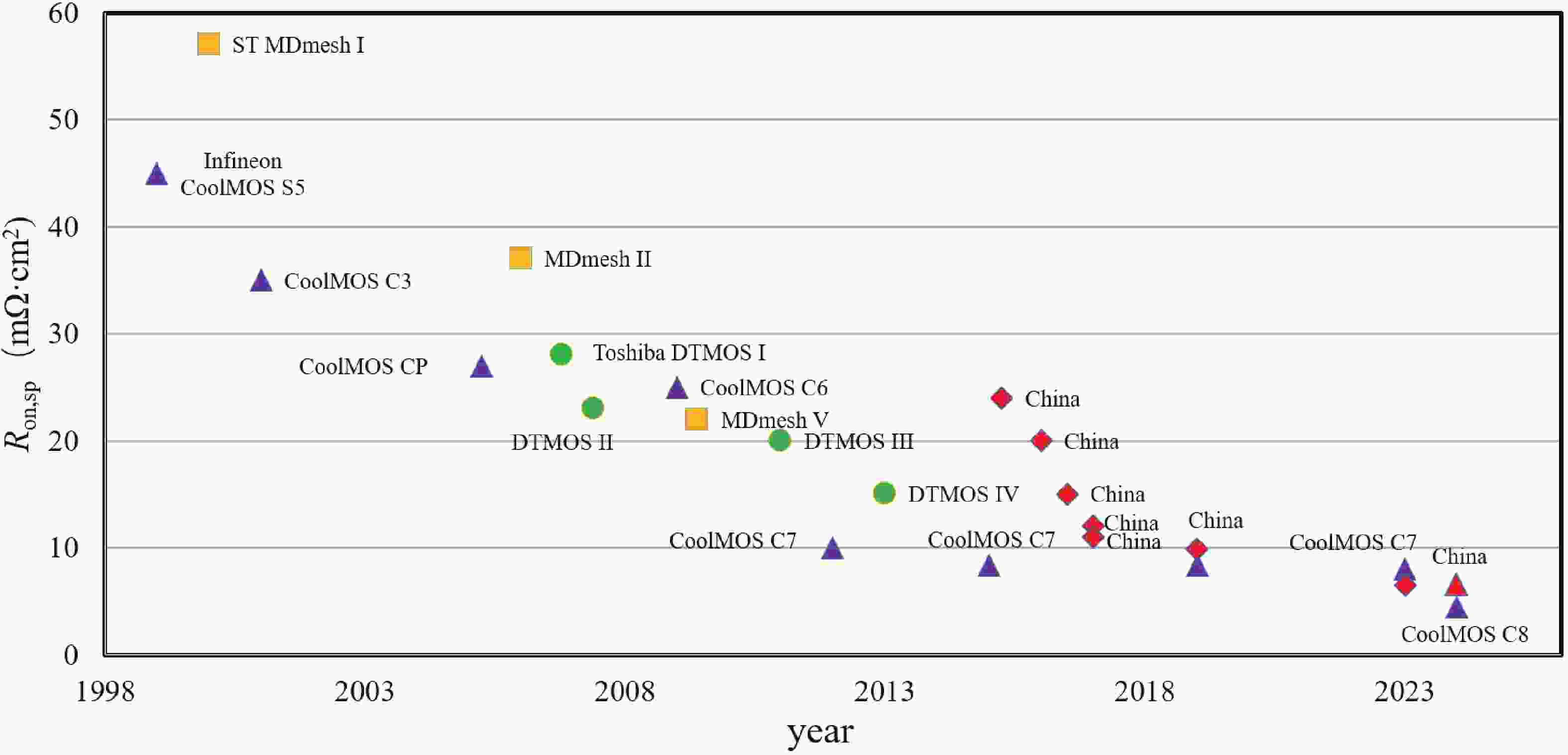
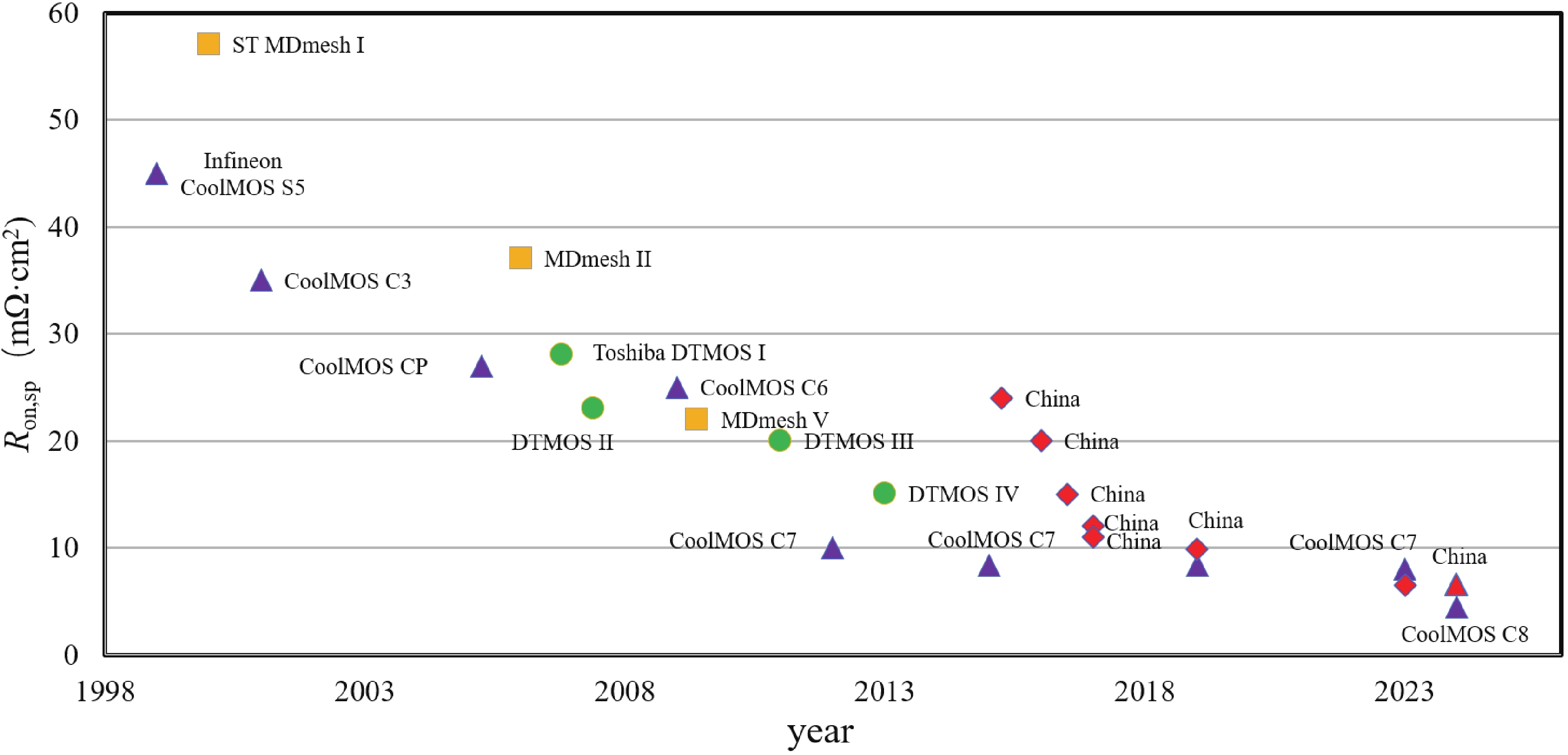
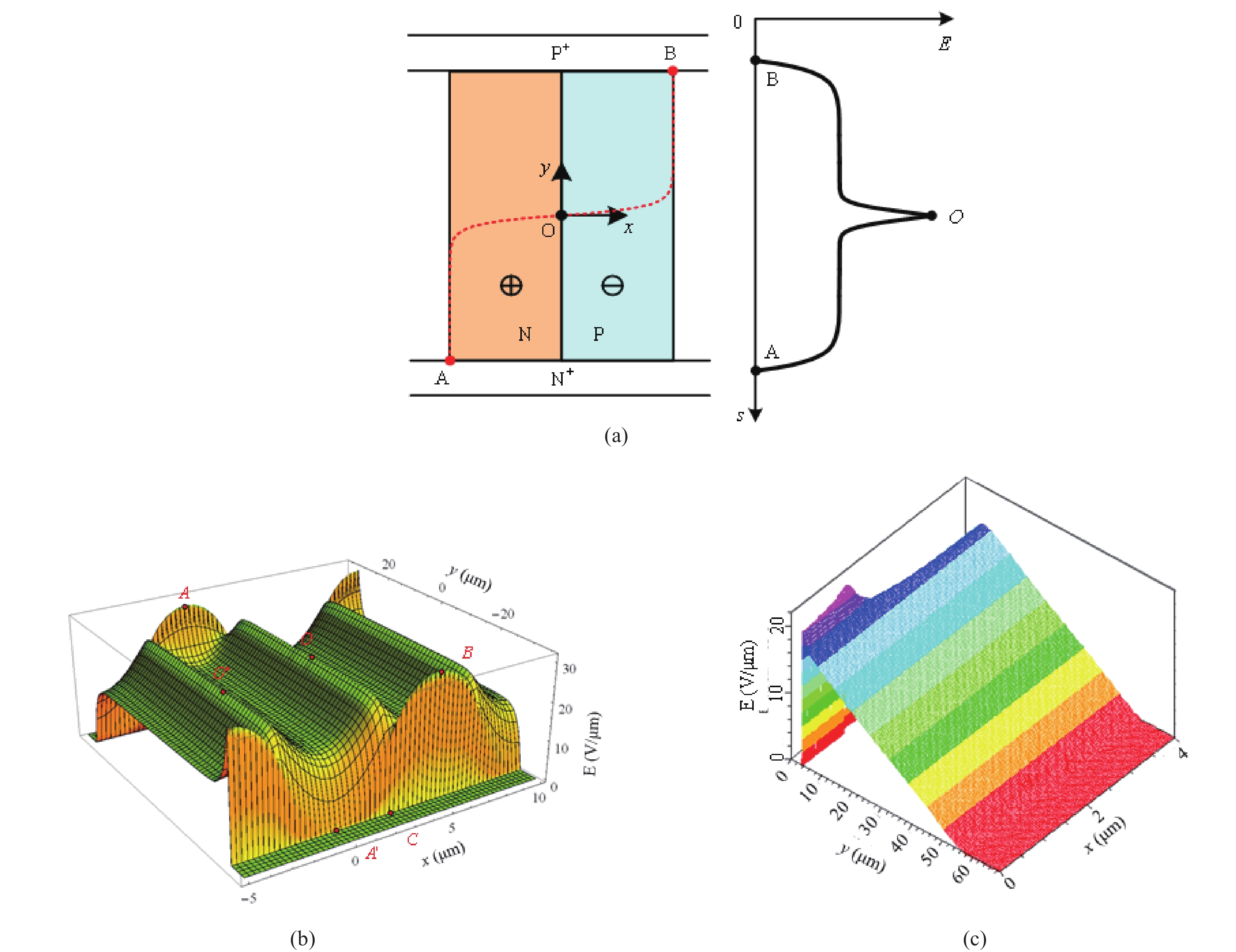
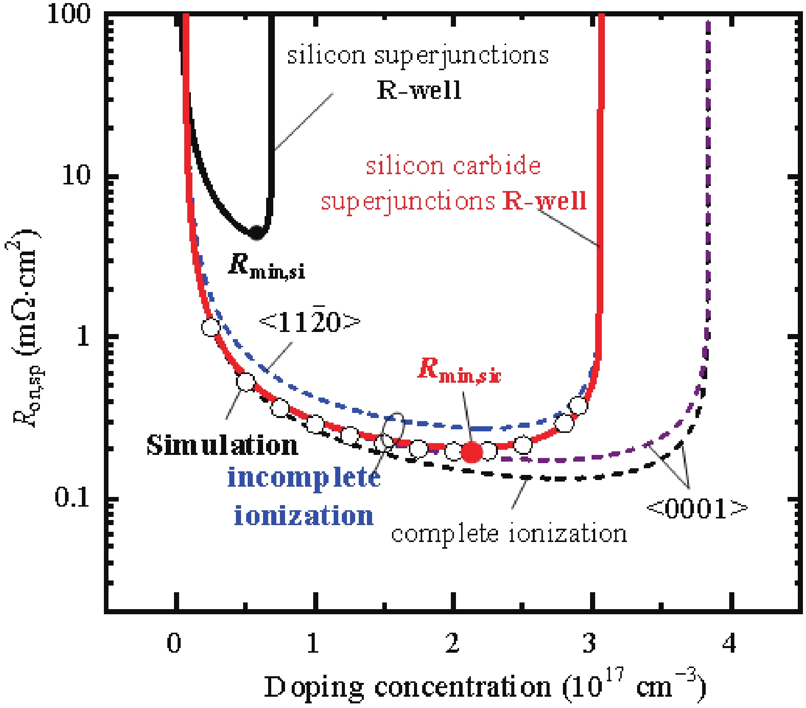
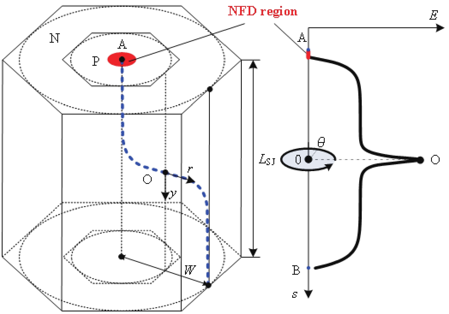
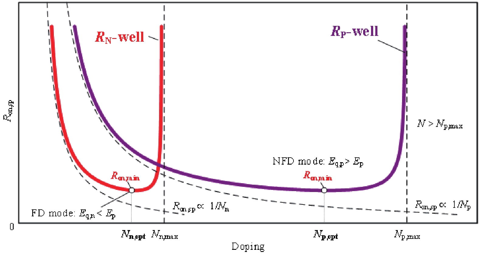
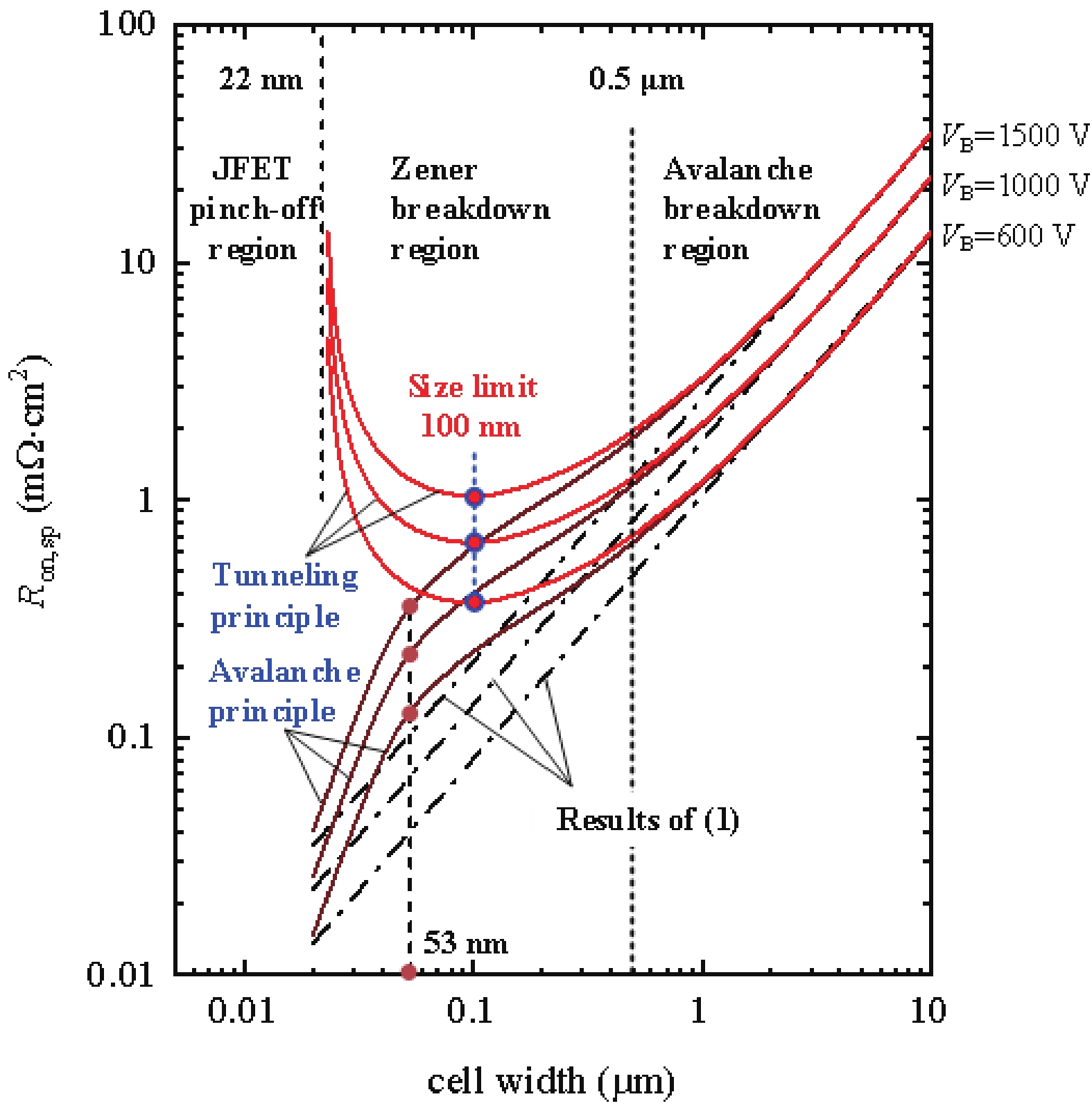
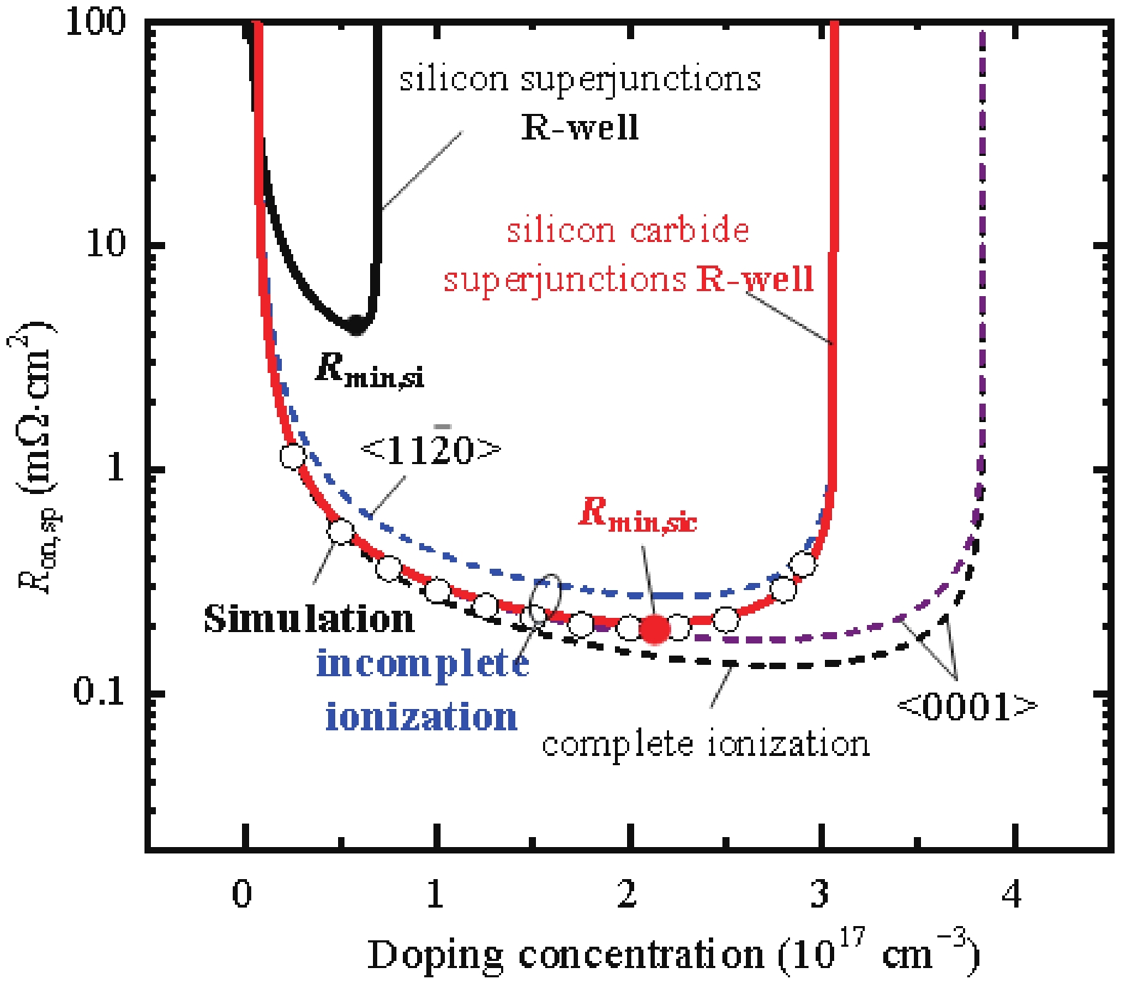
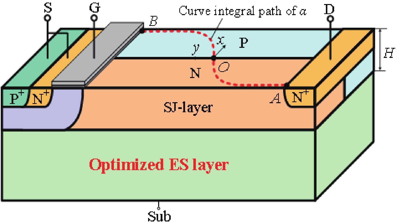
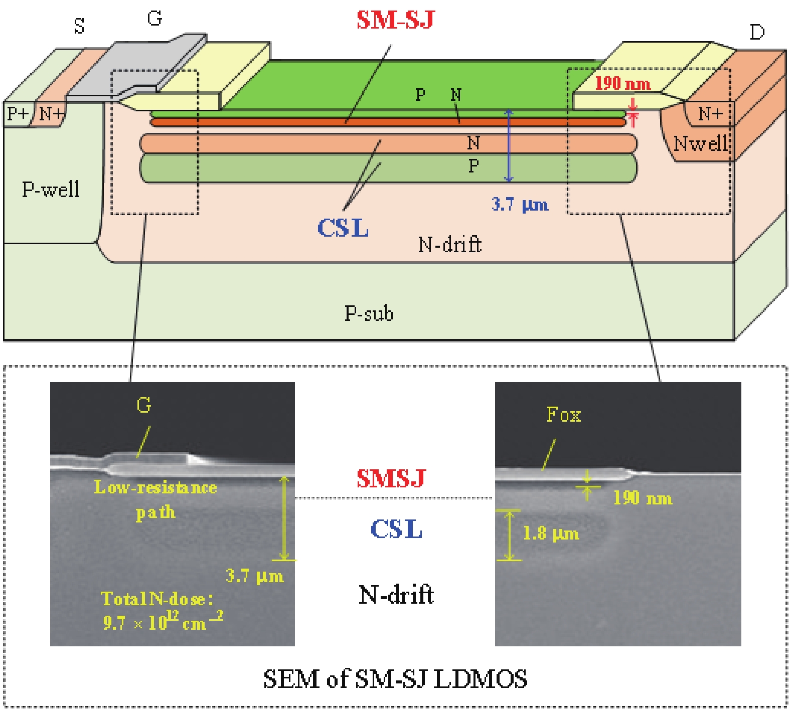
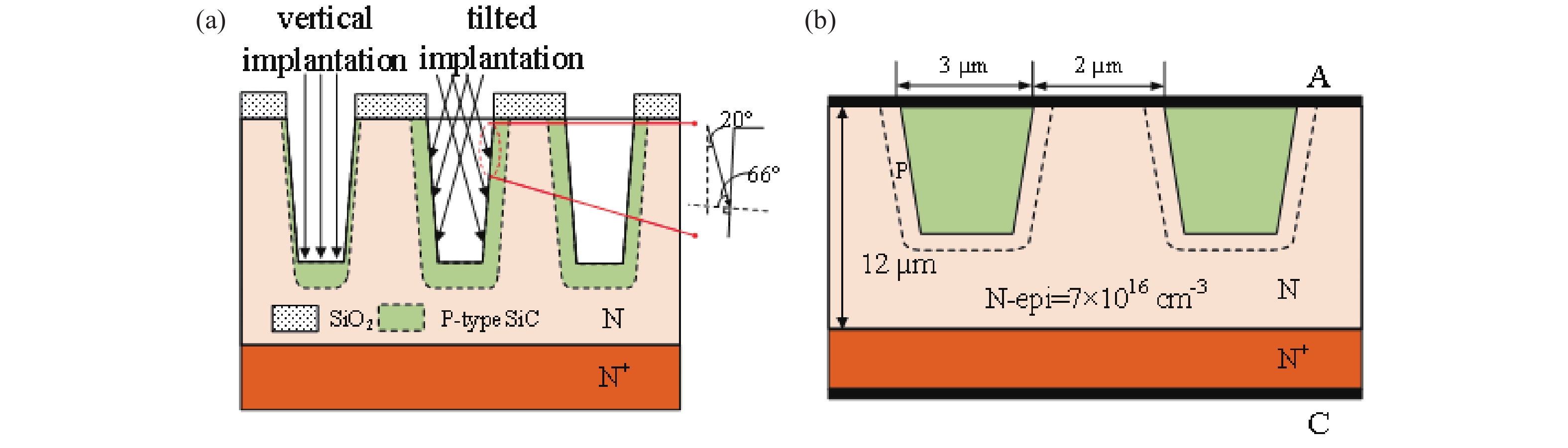
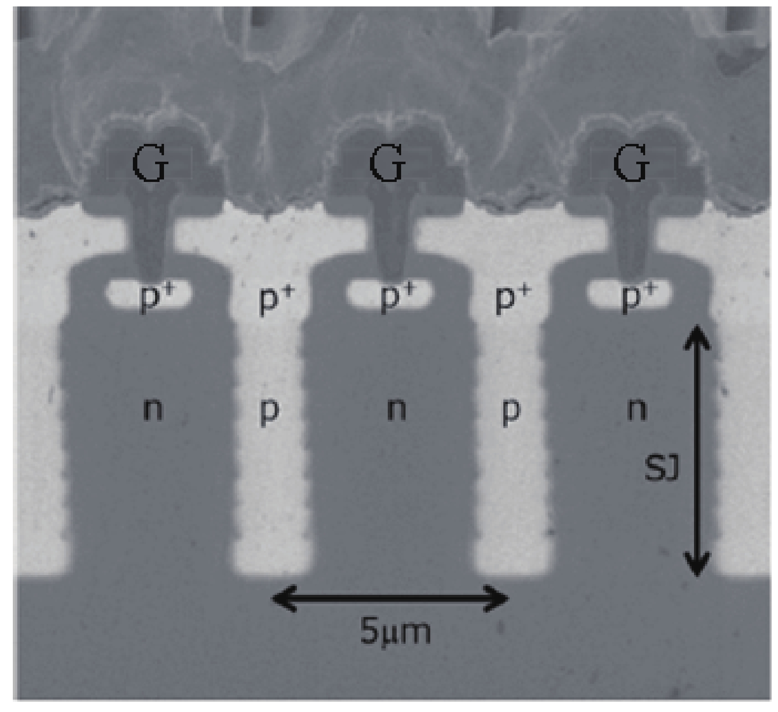
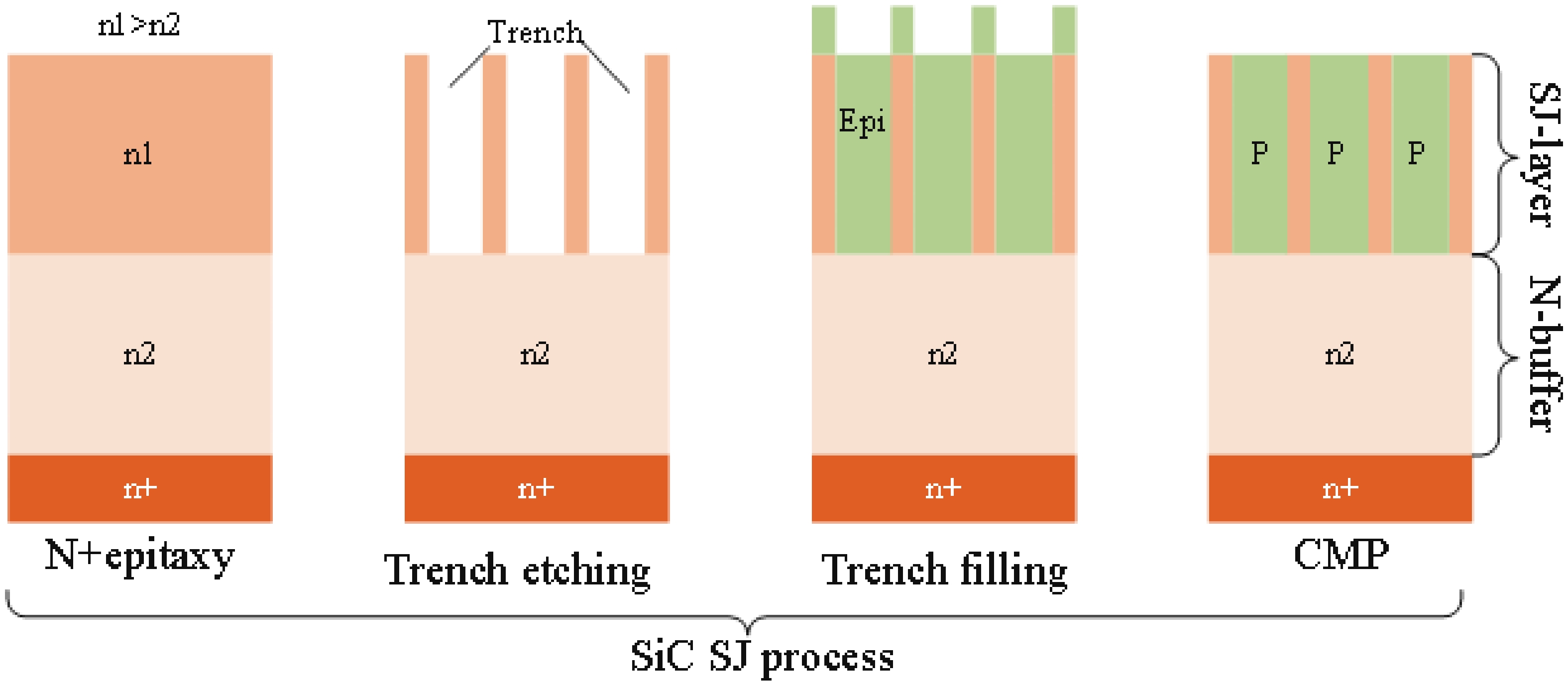
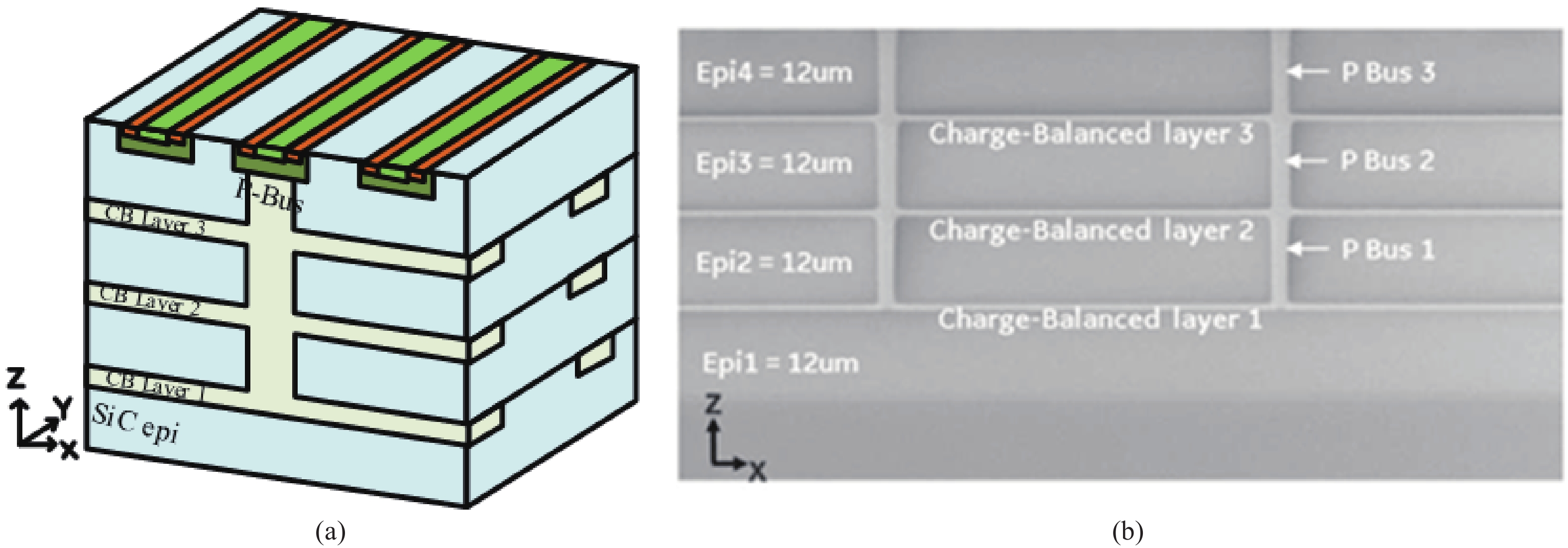
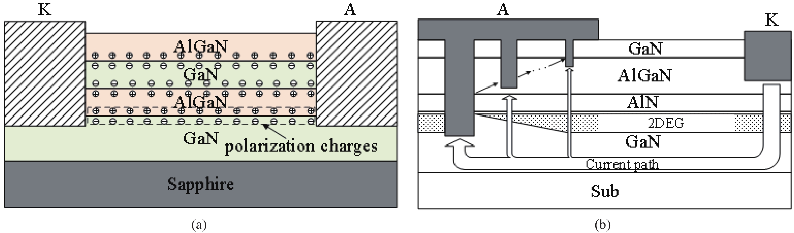
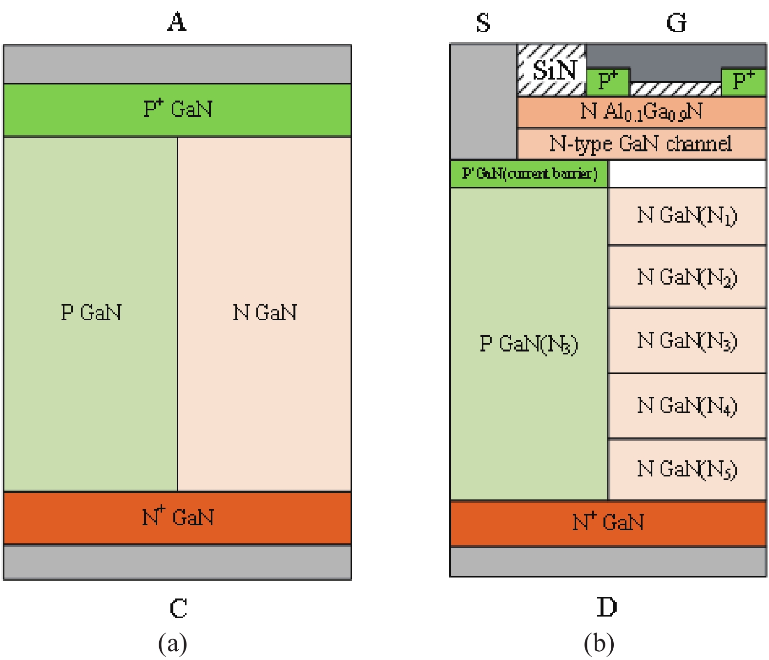
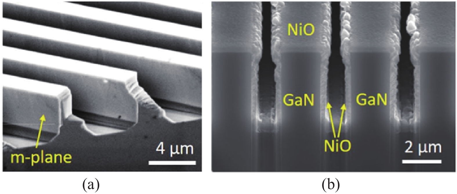
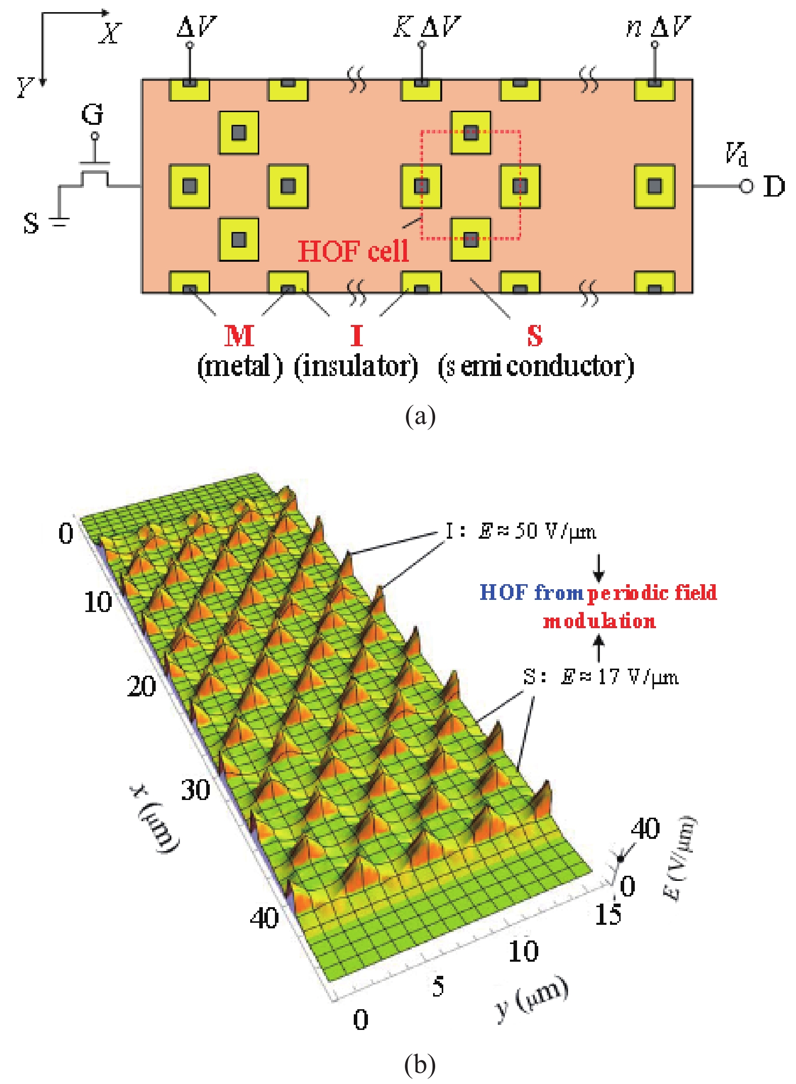
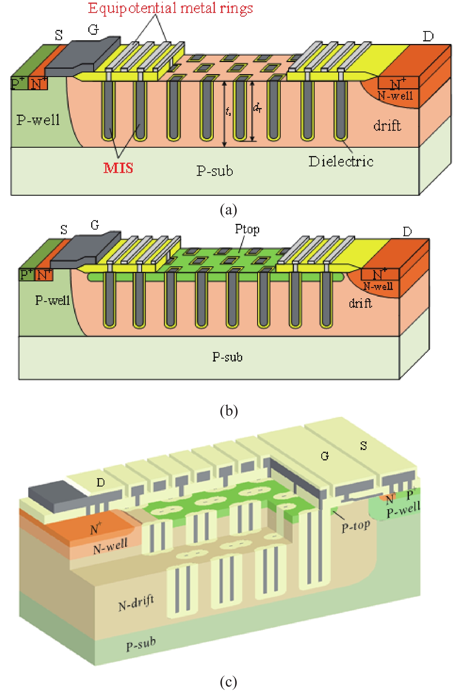
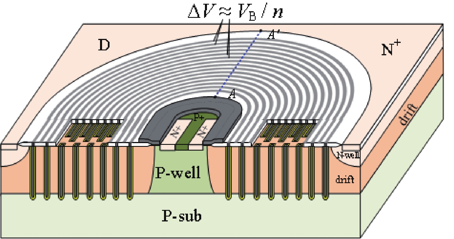
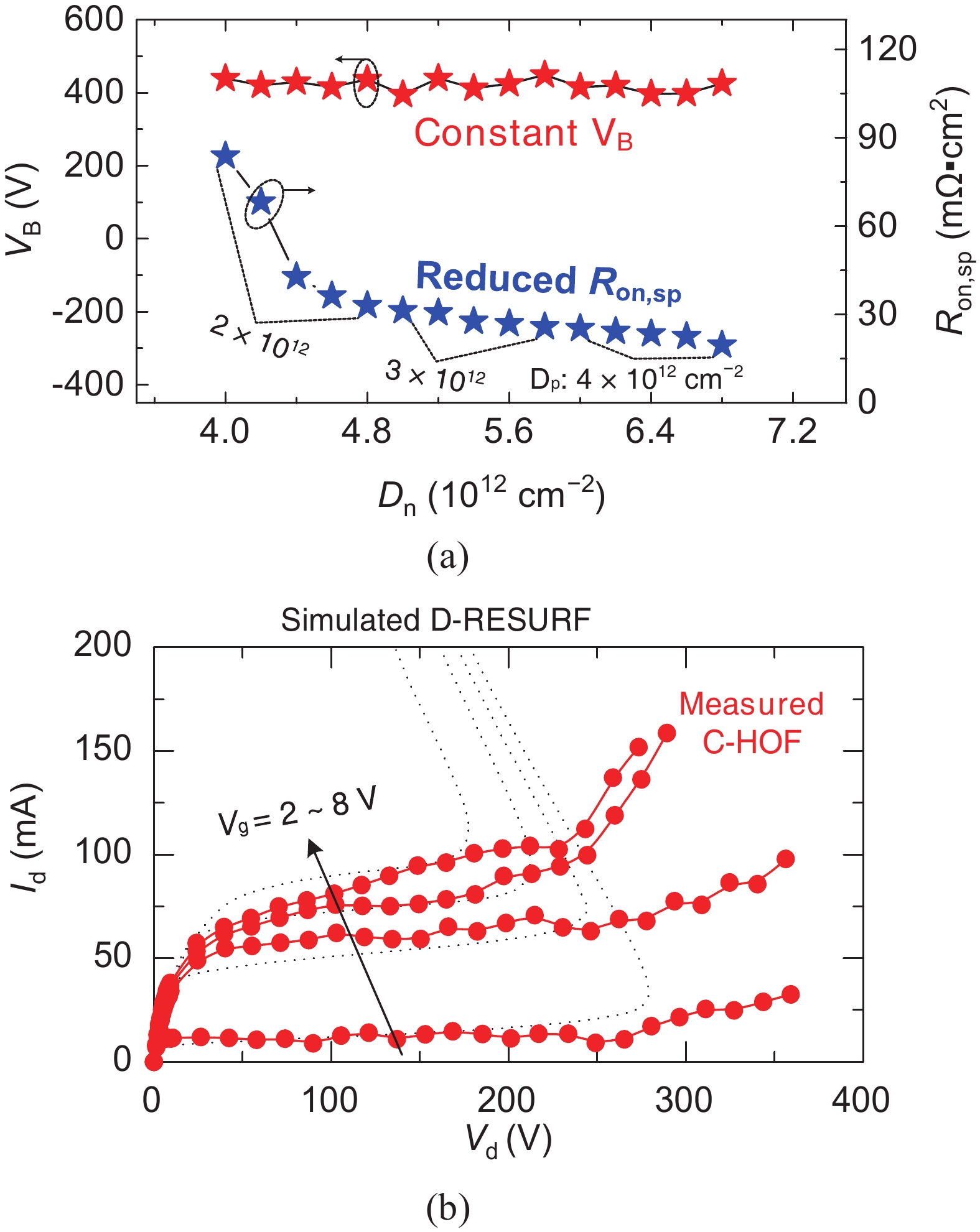
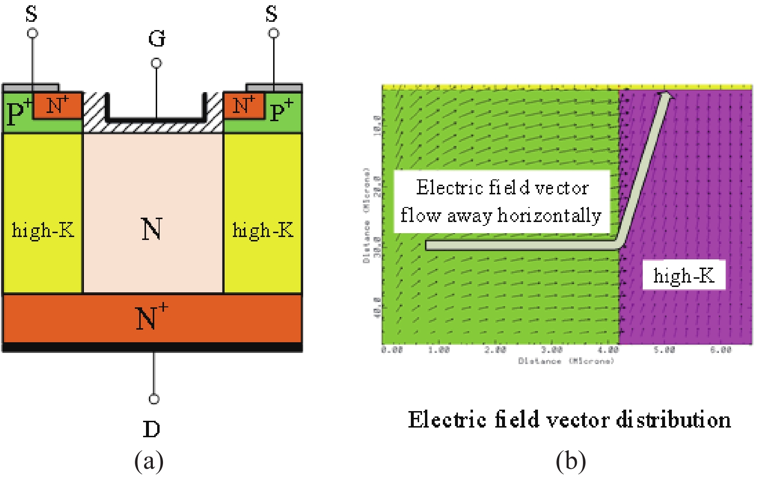
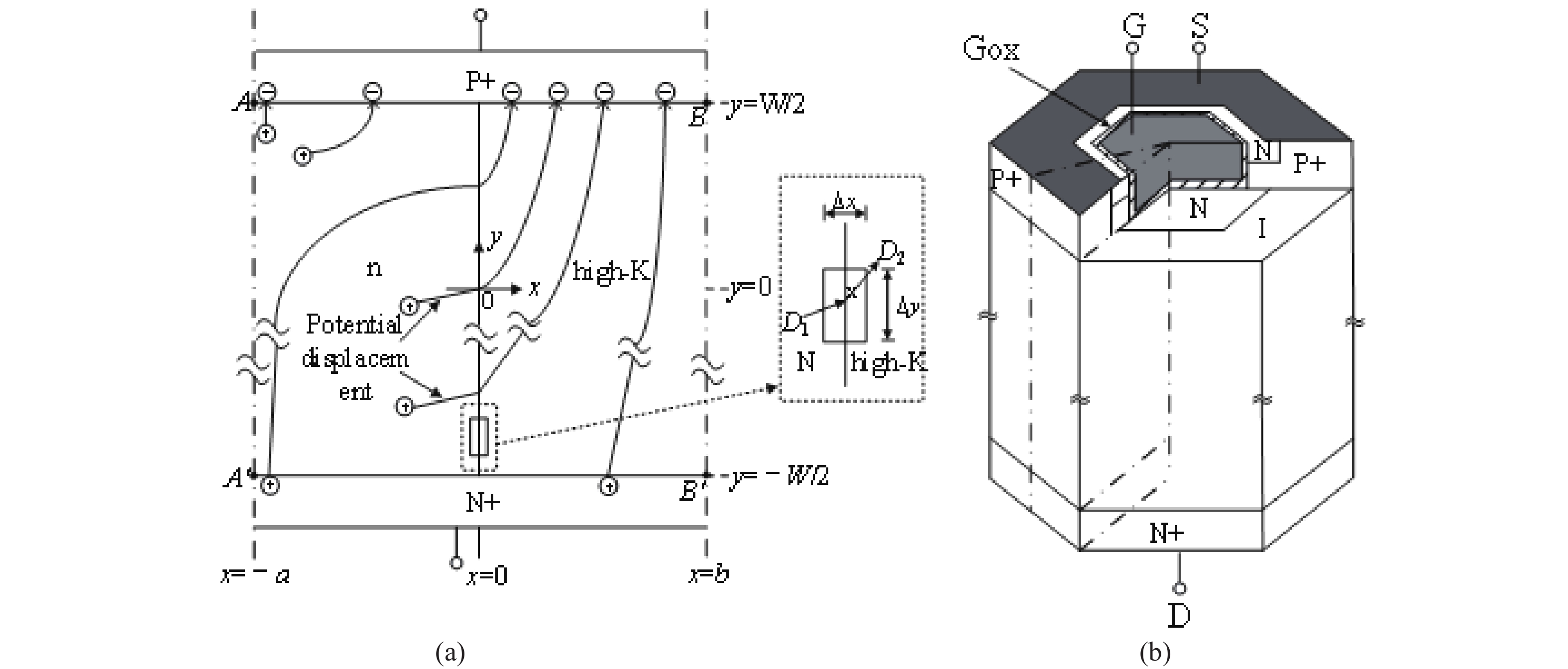
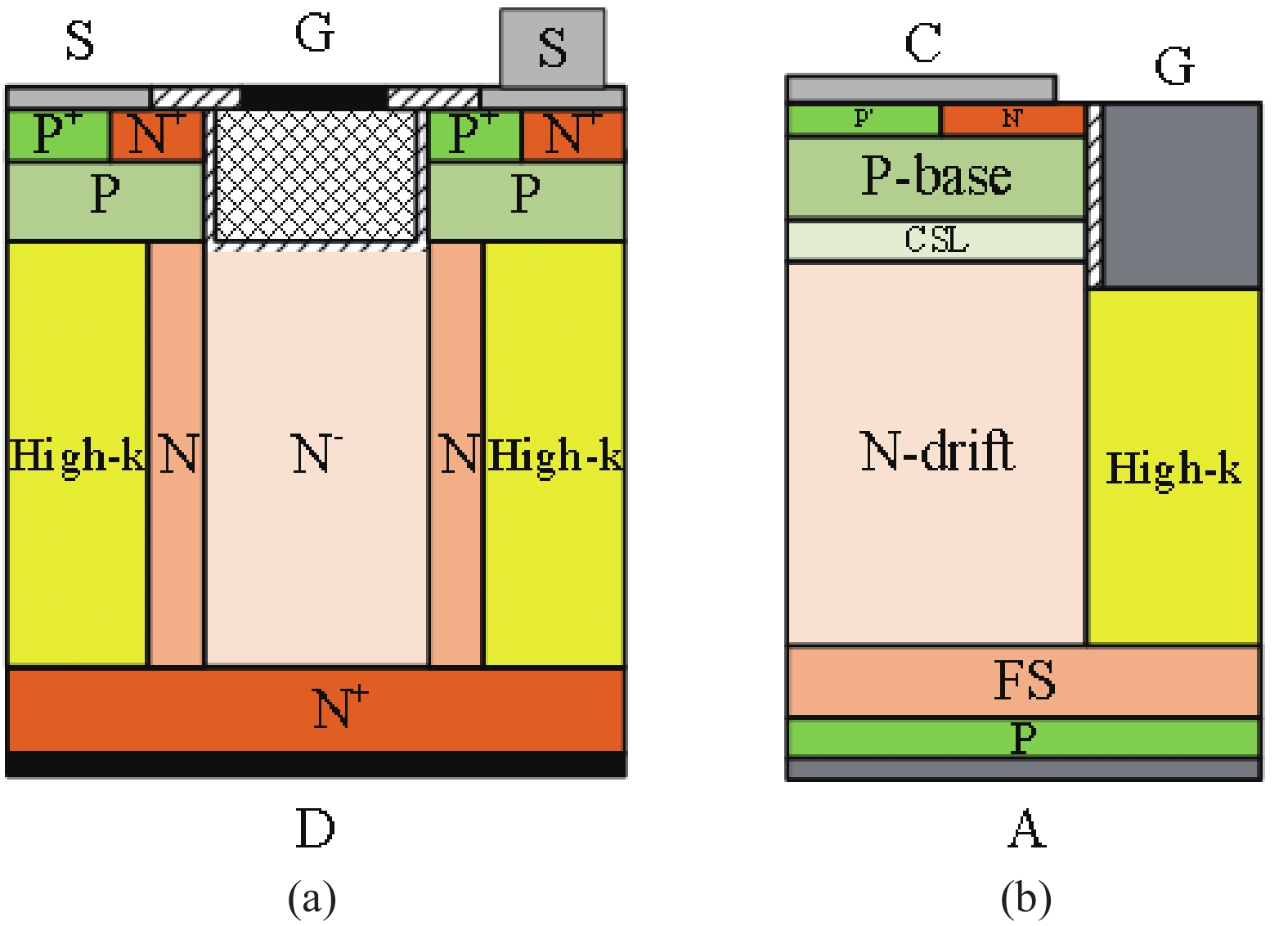
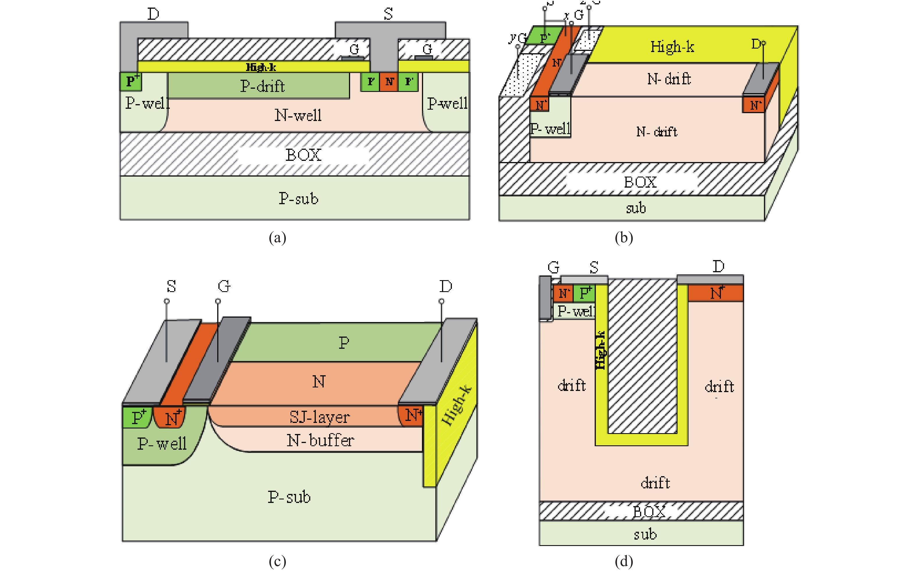
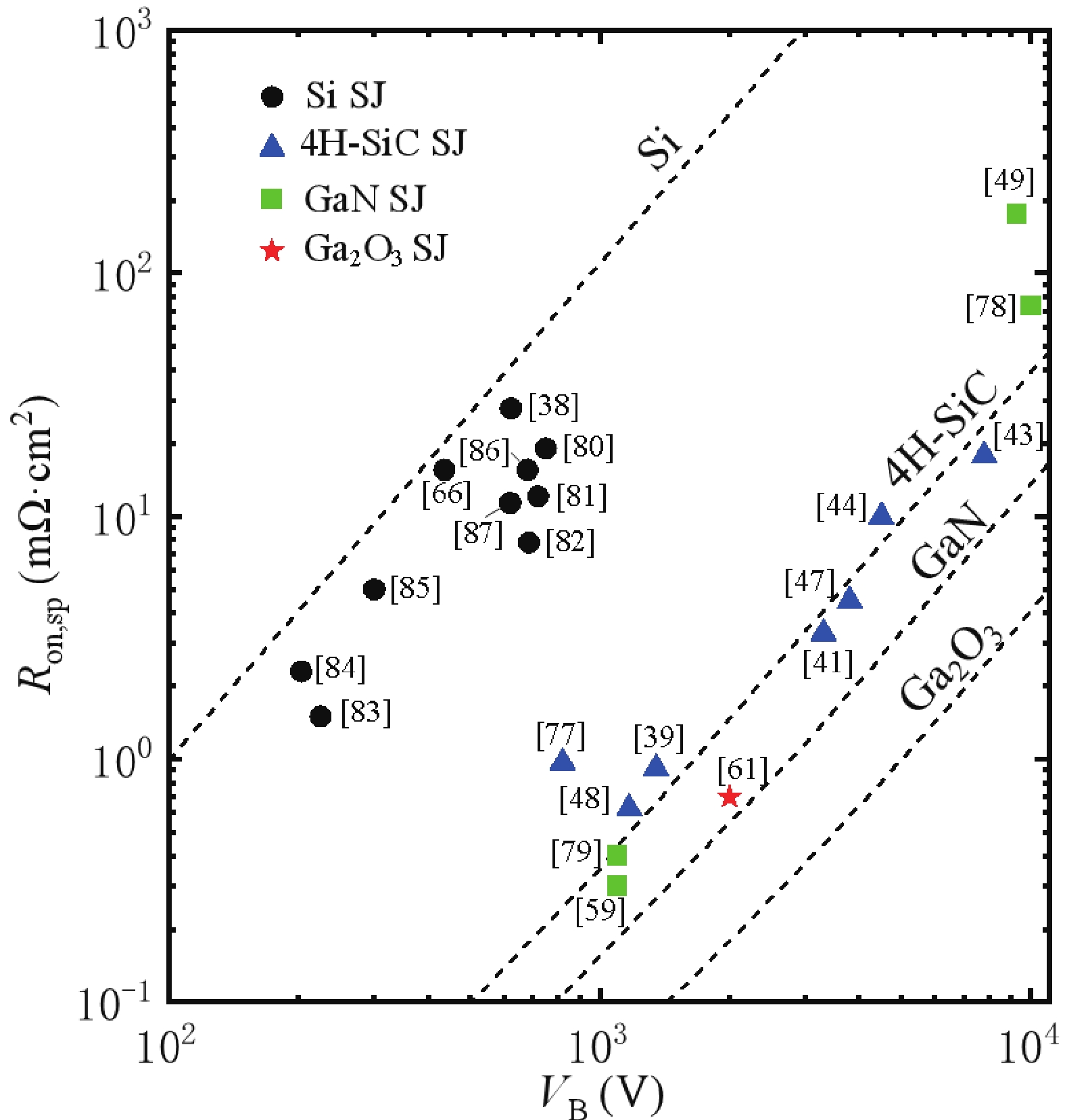
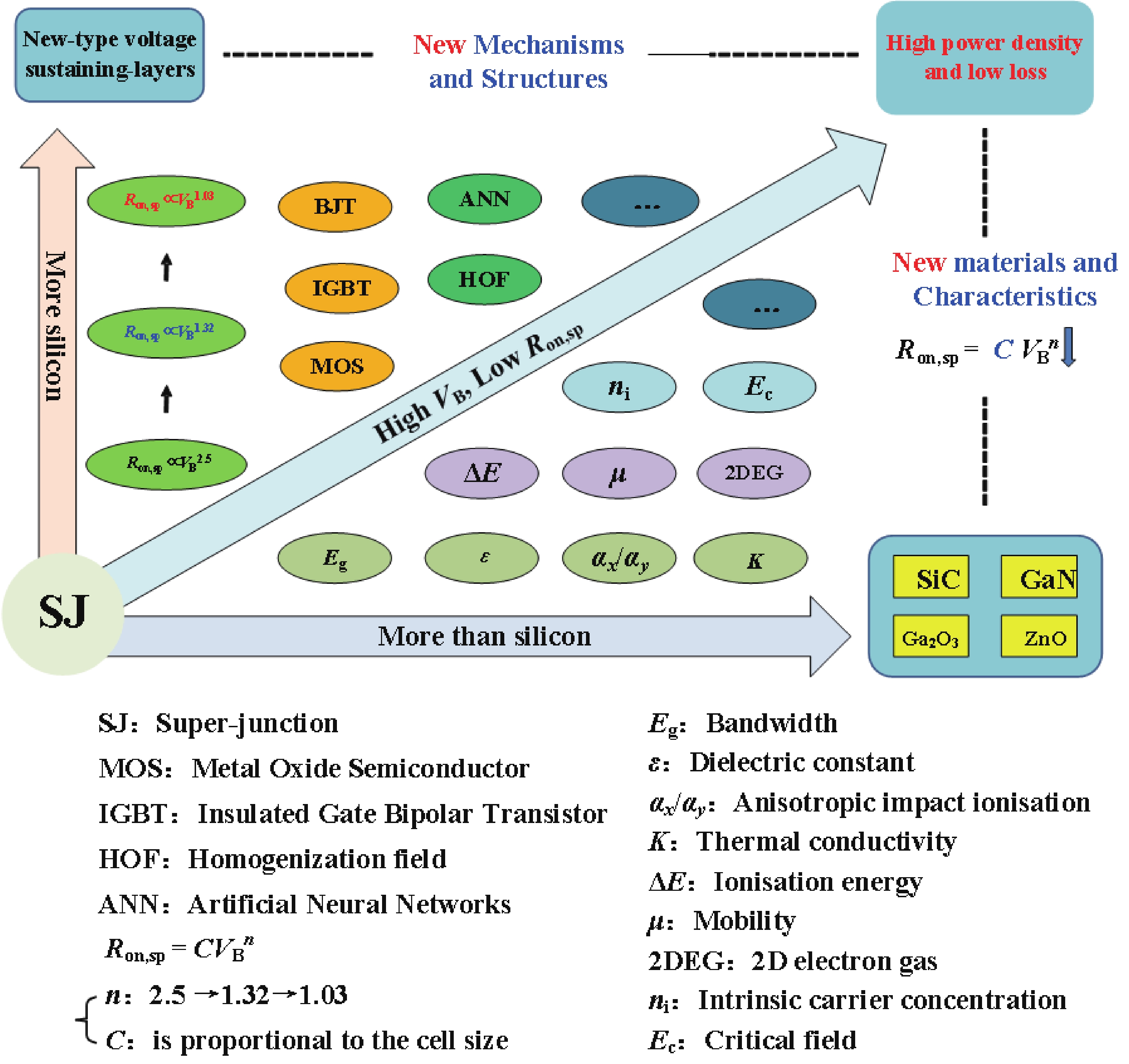
Superjunction (SJ) is one of the most innovative concepts in the field of power semiconductor devices and is often referred to as a "milestone" in power MOS. Its balanced charge field modulation mechanism breaks through the strong dependency between the doping concentration in the drift region and the breakdown voltage VB in conventional devices. This results in a reduction of the trade-off relationship between specific on-resistance Ron,sp and VB from the conventional Ron,sp∝VB2.5 to Ron,sp∝W∙VB1.32, and even to Ron,sp∝W·VB1.03. As the exponential term coefficient decreases, Ron,sp decreases with the cell width W, exhibiting a development pattern reminiscent of "Moore’s Law". This paper provides an overview of the latest research developments in SJ power semiconductor devices. Firstly, it introduces the minimum specific on-resistance Ron,min theory of SJ devices, along with its combination with special effects like 3-D depletion and tunneling, discussing the development of Ron,min theory in the wide bandgap SJ field. Subsequently, it discusses the latest advancements in silicon-based and wide bandgap SJ power devices. Finally, it introduces the homogenization field (HOF) and high-K voltage-sustaining layers derived from the concept of SJ charge balance. SJ has made significant progress in device performance, reliability, and integration, and in the future, it will continue to evolve through deeper integration with different materials, processes, and packaging technologies, enhancing the overall performance of semiconductor power devices.
J. Semicond.
2024, 45(11): 111801 doi: 10.1088/1674-4926/24050029
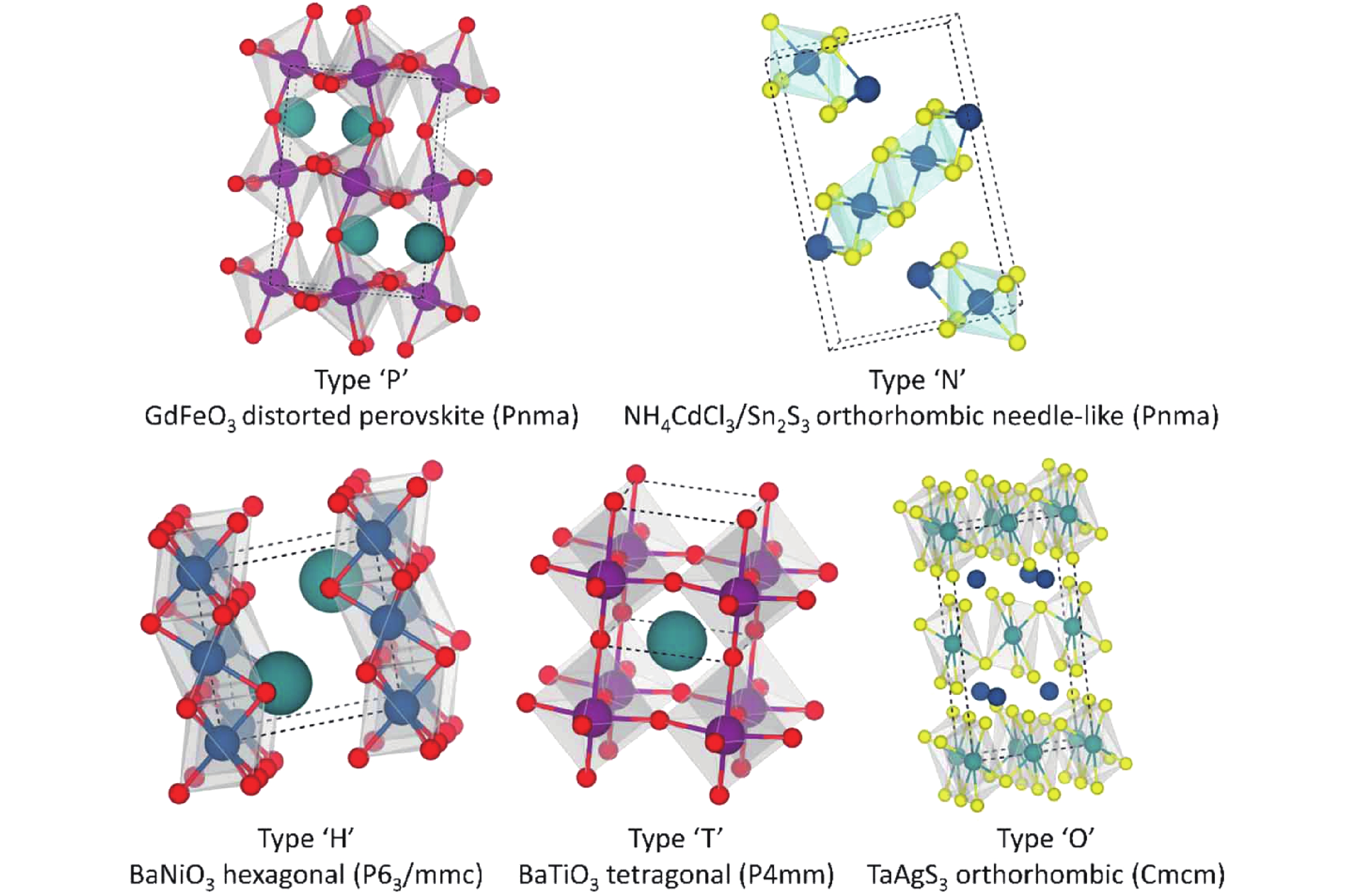
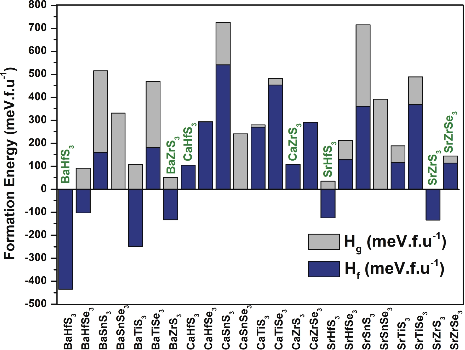
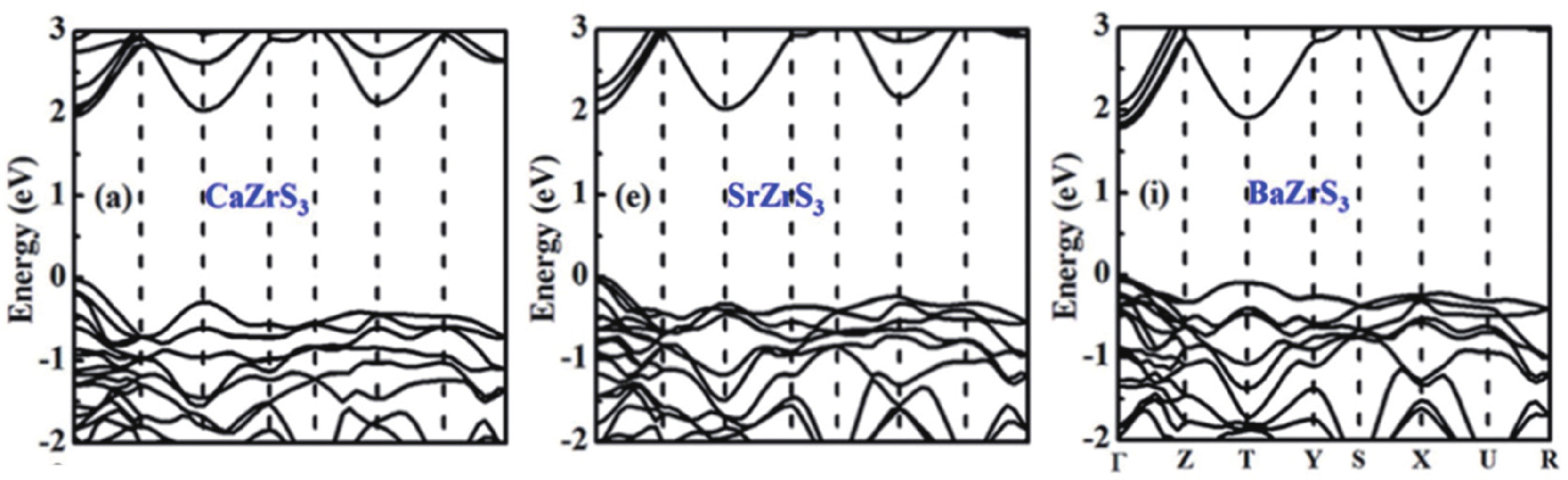
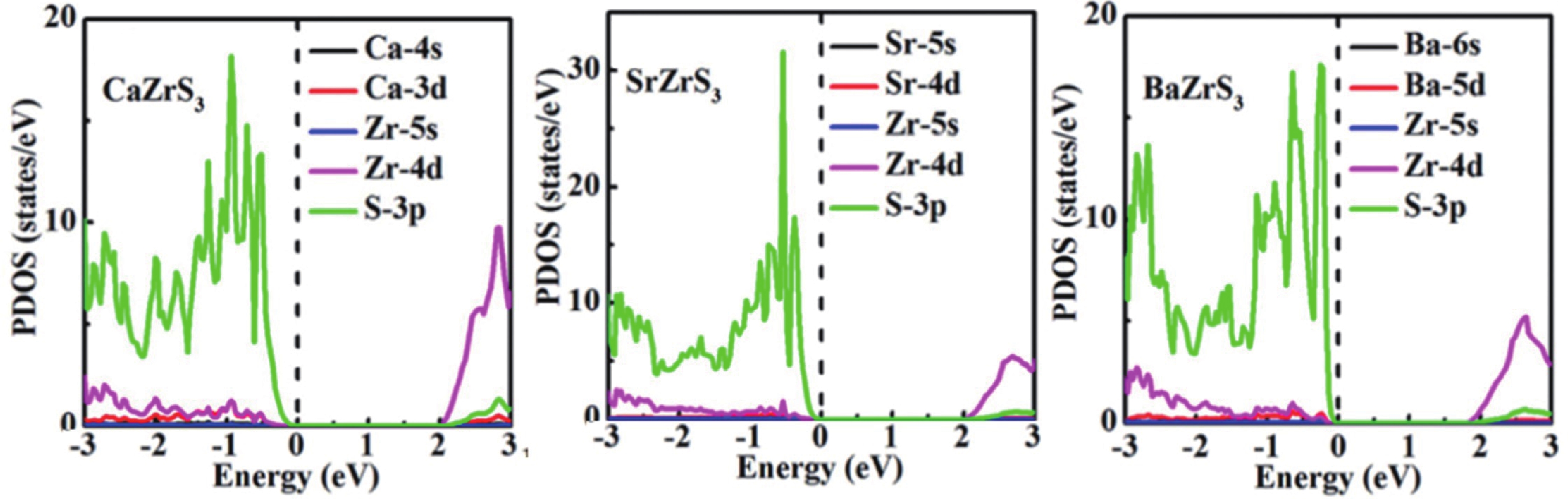
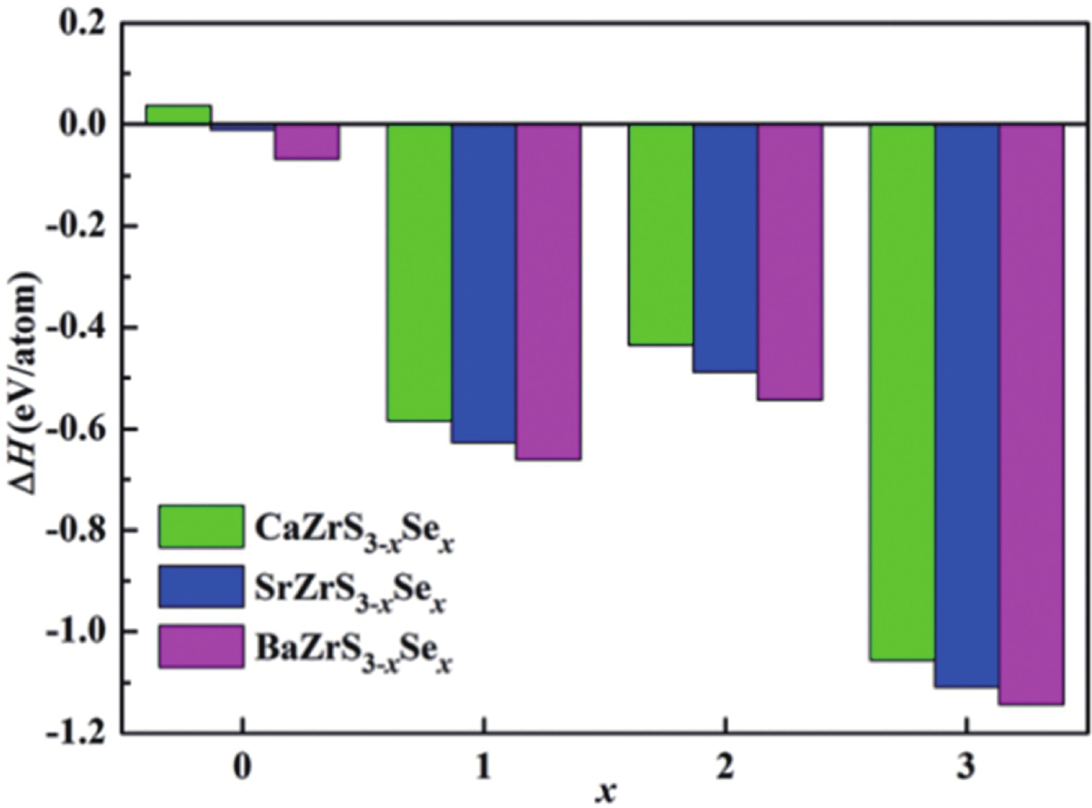
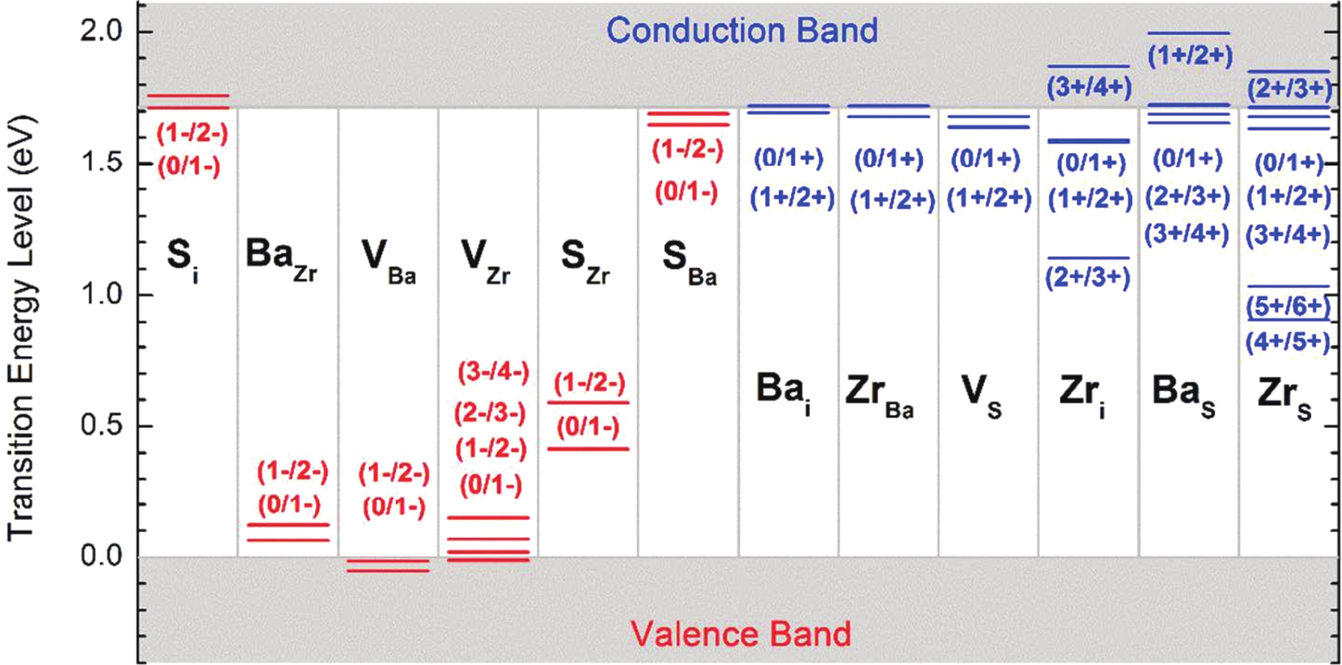
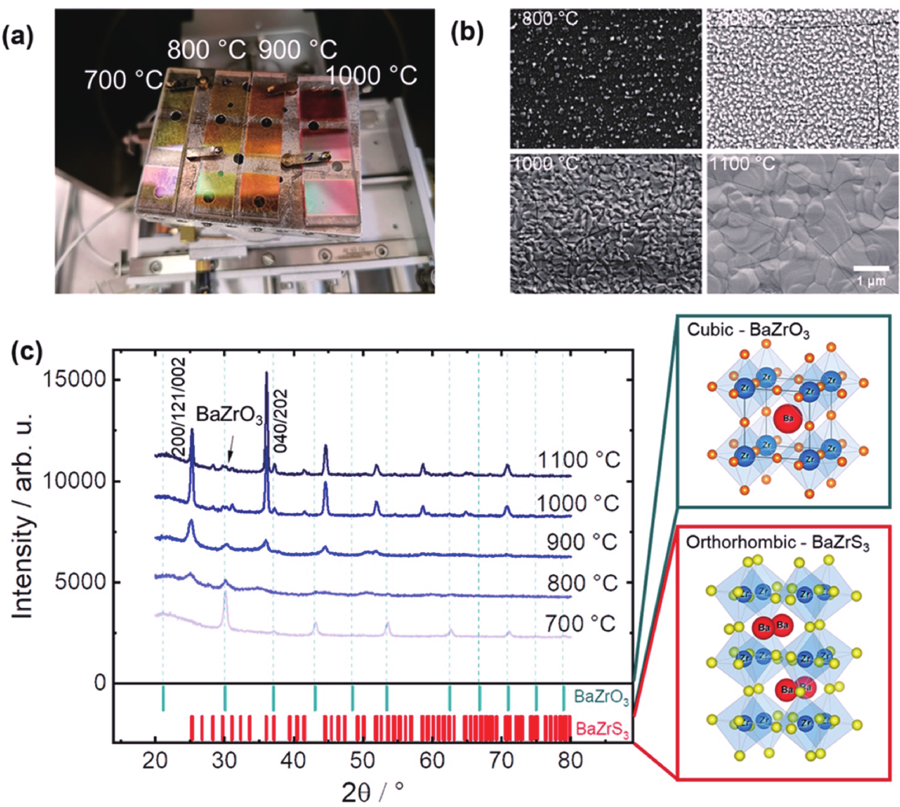
Perovskites dominate the photovoltaic research community over the last two decades due to its very high absorption coefficient, electron and hole mobility. However, most of the reported solar cells constitute organic perovskites which offer very high efficiency but are highly unstable. Chalcogenide perovskites like BaZrS3, CaZrS3, etc. promise to be a perfect alternate owing to its high stability and mobilities. But, till now no stable photovoltaic device has been successfully fabricated using these materials and the existing challenges present in the synthesis of such perovskites are discussed. Also, the basic thermodynamic aspects that are essential for formation of BaZrS3 are discussed. An extensive review on the precedent literatures and the future direction in the BaZrS3 photovoltaic device research is clearly given.
J. Semicond.
2024, 45(11): 112101 doi: 10.1088/1674-4926/24050032
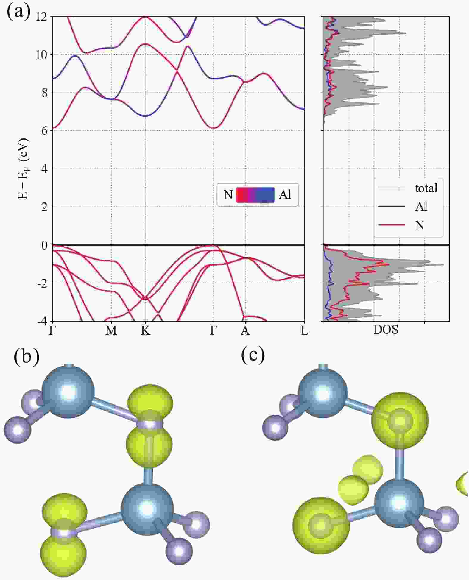
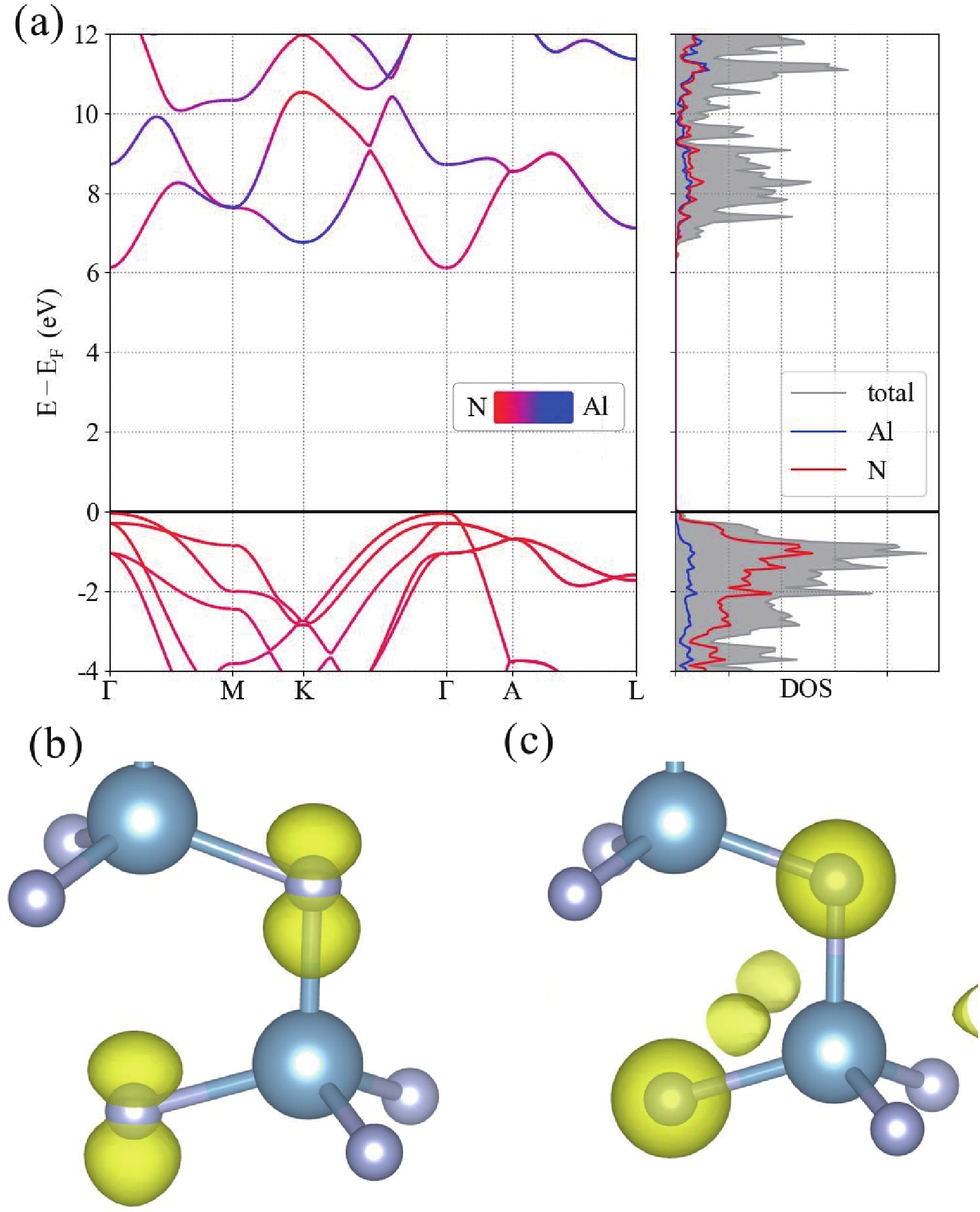
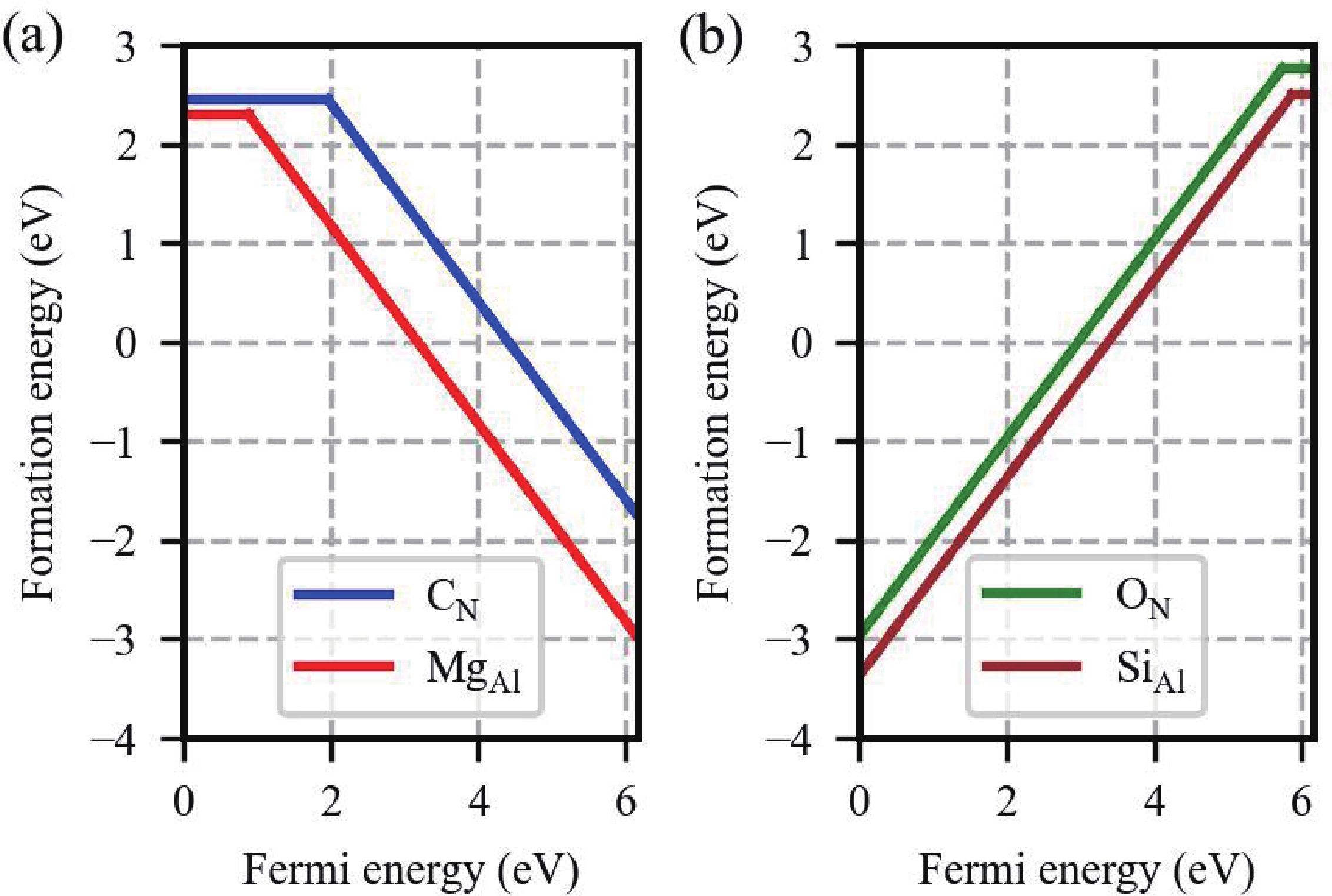
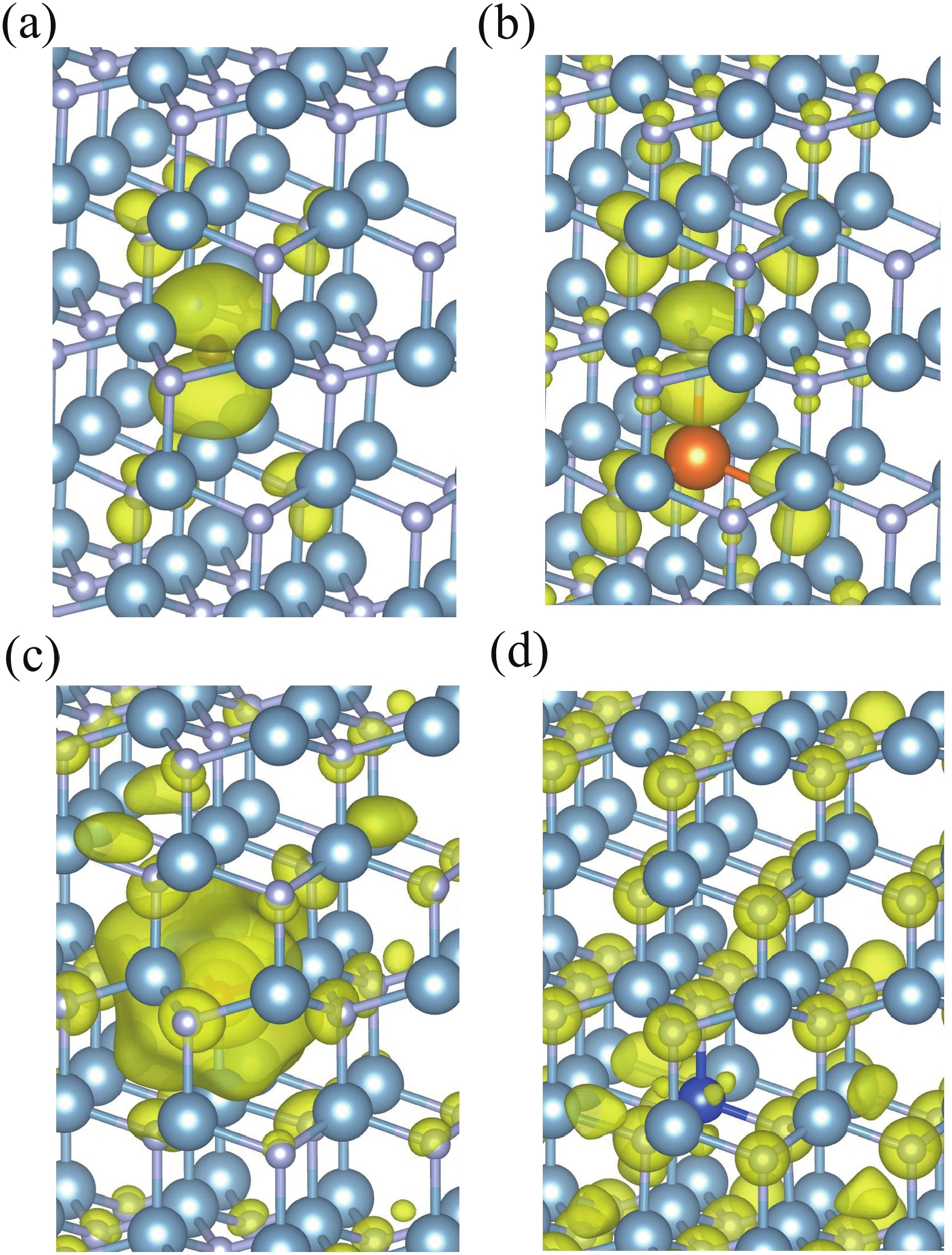
The choices of proper dopants and doping sites significantly influence the doping efficiency. In this work, using doping in AlN as an example, we discuss how to choose dopants and doping sites in semiconductors to create shallow defect levels. By comparing the defect properties of CN, ON, MgAl, and SiAl in AlN and analyzing the pros and cons of different doping approaches from the aspects of size mismatch between dopant and host elements, electronegativity difference and perturbation to the band edge states after the substitution, we propose that MgAl and SiAl should be the best dopants and doping sites for p-type and n-type doping, respectively. Further first-principles calculations verify our predictions as these defects present lower formation energies and shallower defect levels. The defect charge distributions also show that the band edge states, which mainly consist of N- s and p orbitals, are less perturbed when Al is substituted, therefore, the derived defect states turn out to be delocalized, opposite to the situation when N is substituted. This approach of analyzing the band structure of the host material and choosing dopants and doping sites to minimize the perturbation on the host band structure is general and can provide reliable estimations for finding shallow defect levels in semiconductors.
J. Semicond.
2024, 45(11): 112102 doi: 10.1088/1674-4926/24040023
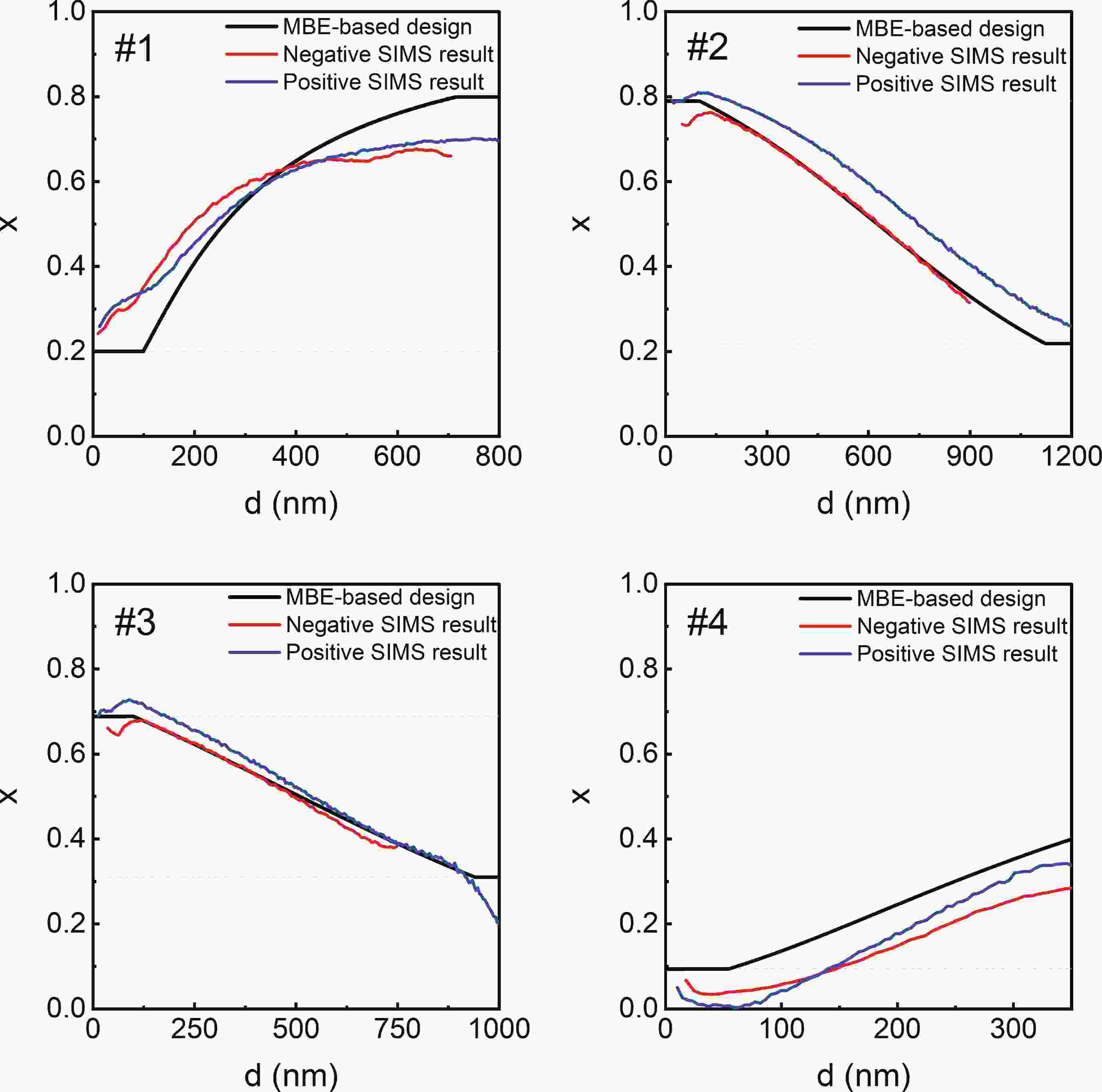
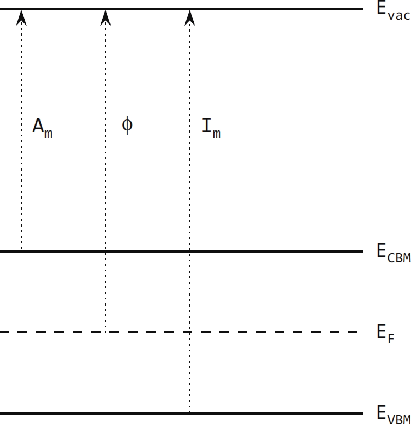
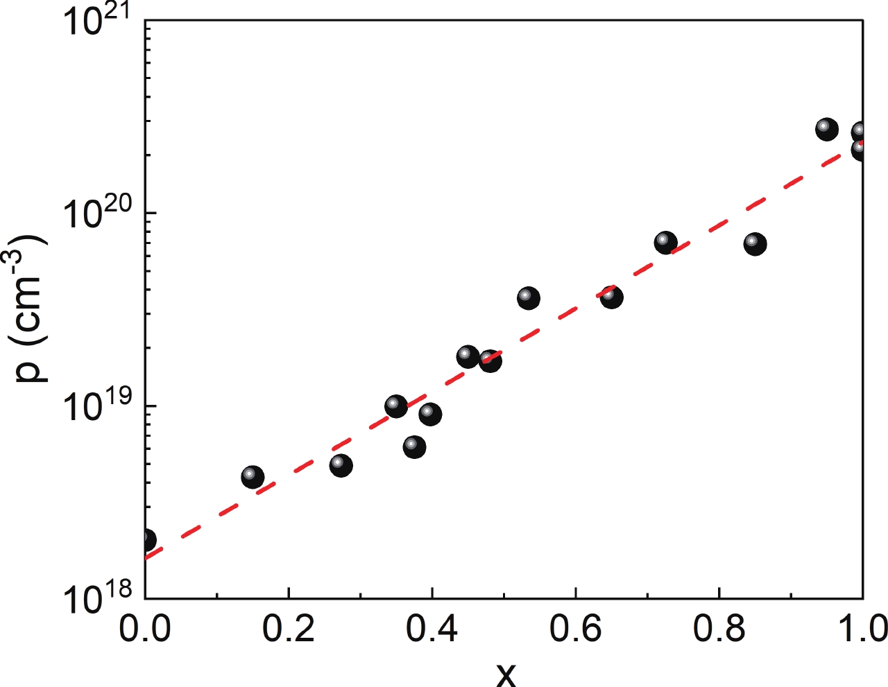
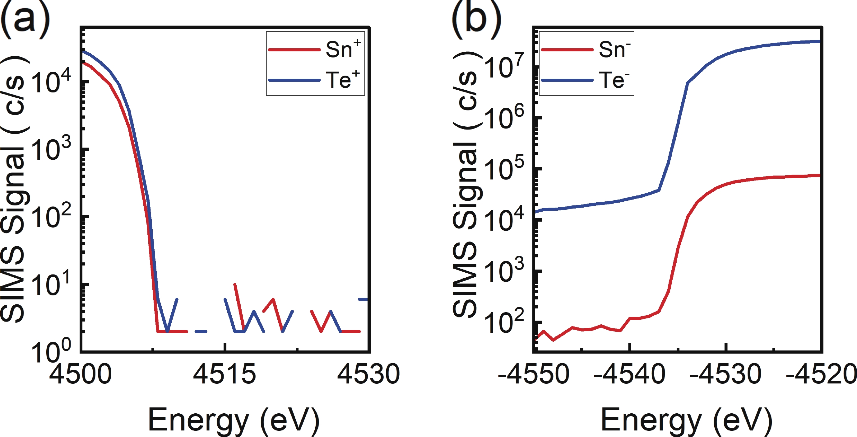
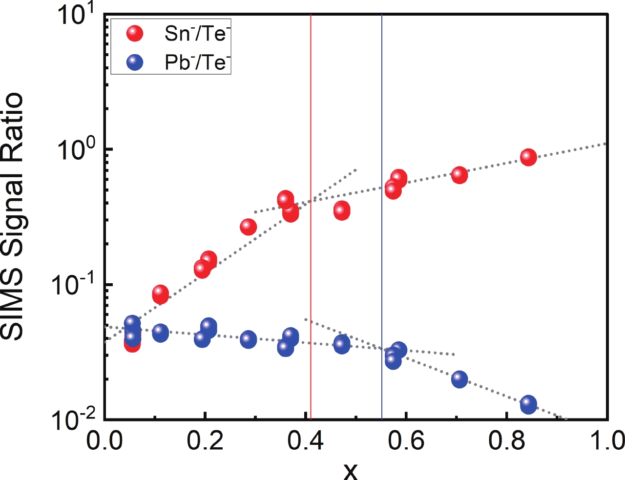
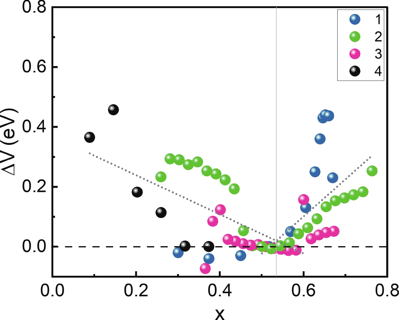
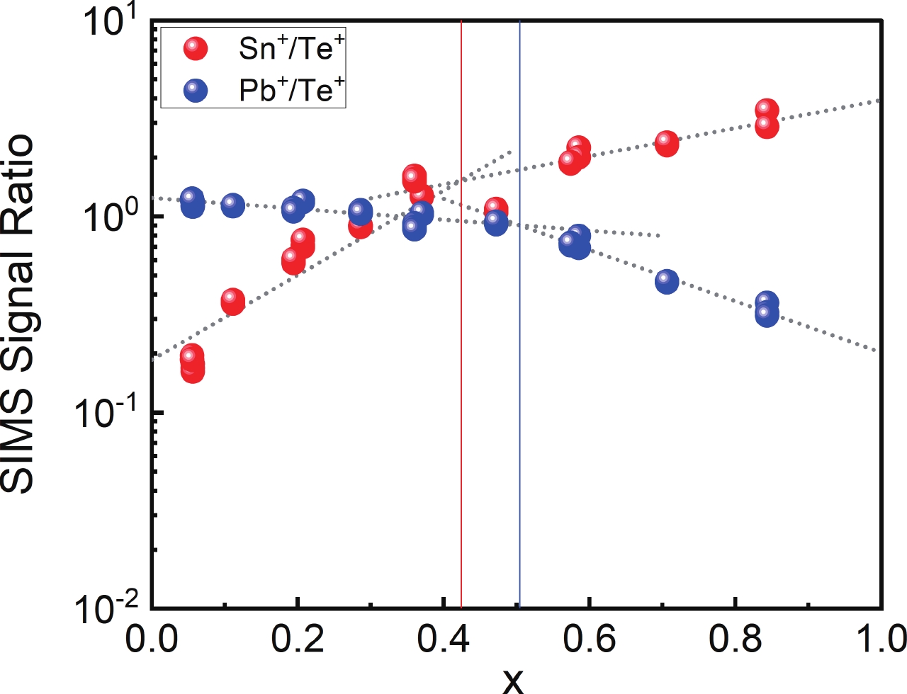
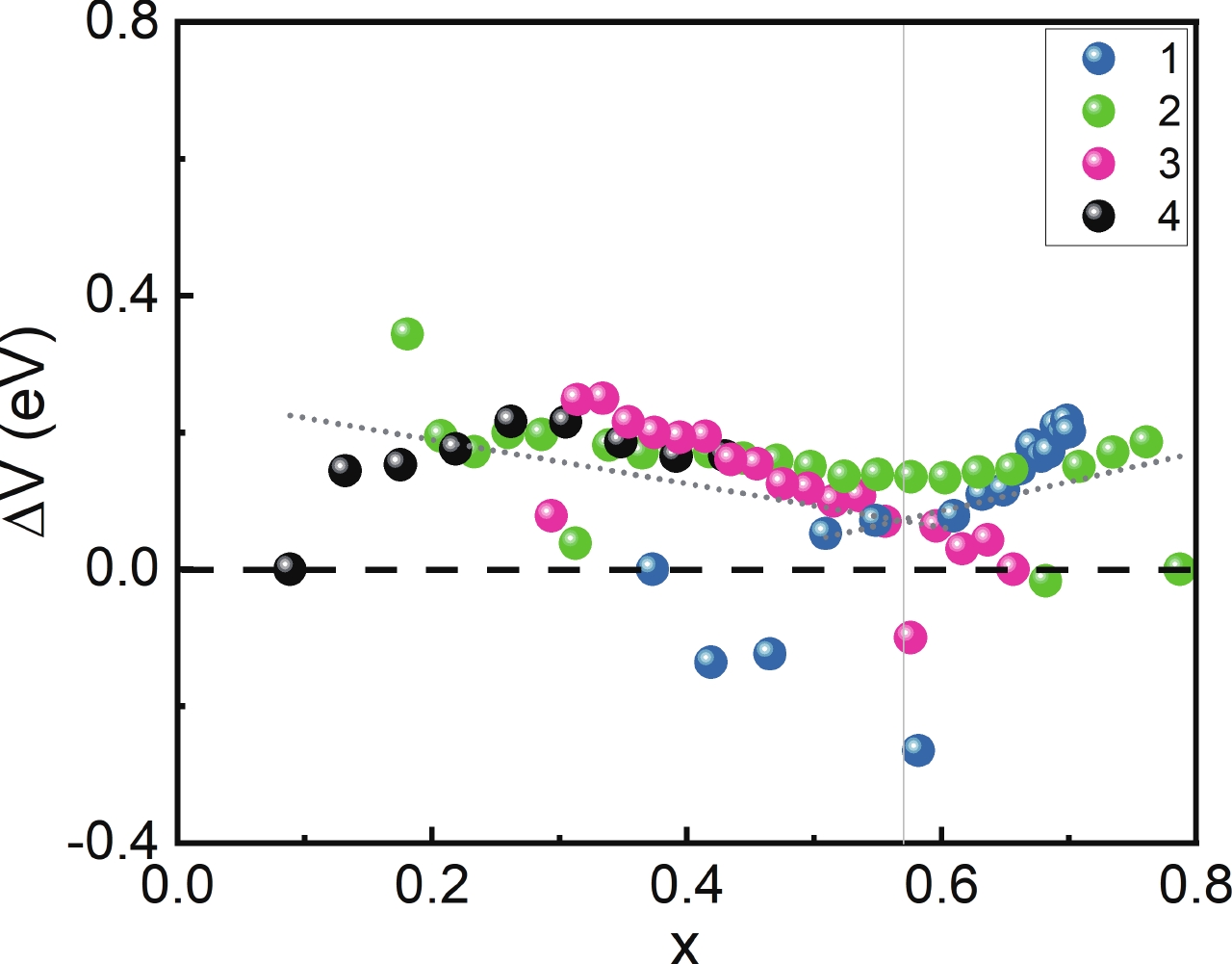
This paper introduces a pioneering application of secondary ion mass spectrometry (SIMS) for estimating the electronic properties of Pb1−xSnxTe, a compound categorized as a topological crystalline insulator. The proposed approach marks the first application of SIMS for such estimations and focuses on investigating variations in ionization probabilities and shifts in the energy distribution of secondary ions. The ionization probabilities are influenced by pivotal parameters such as the material's work function and electron affinity. The derivation of these parameters hinges upon the energy gap's positioning relative to the vacuum level for varying values of $ x $ within the Pb1−xSnxTe compound. The findings elucidate noteworthy alterations in SIMS signals, particularly near the critical point of band-gap closing.
J. Semicond.
2024, 45(11): 112301 doi: 10.1088/1674-4926/24060007

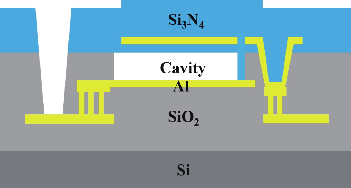
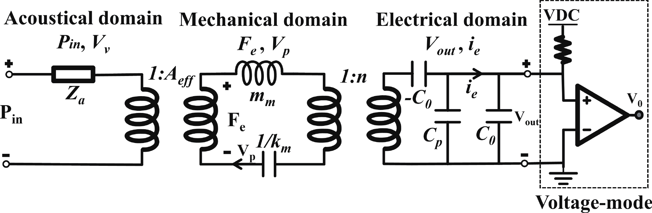
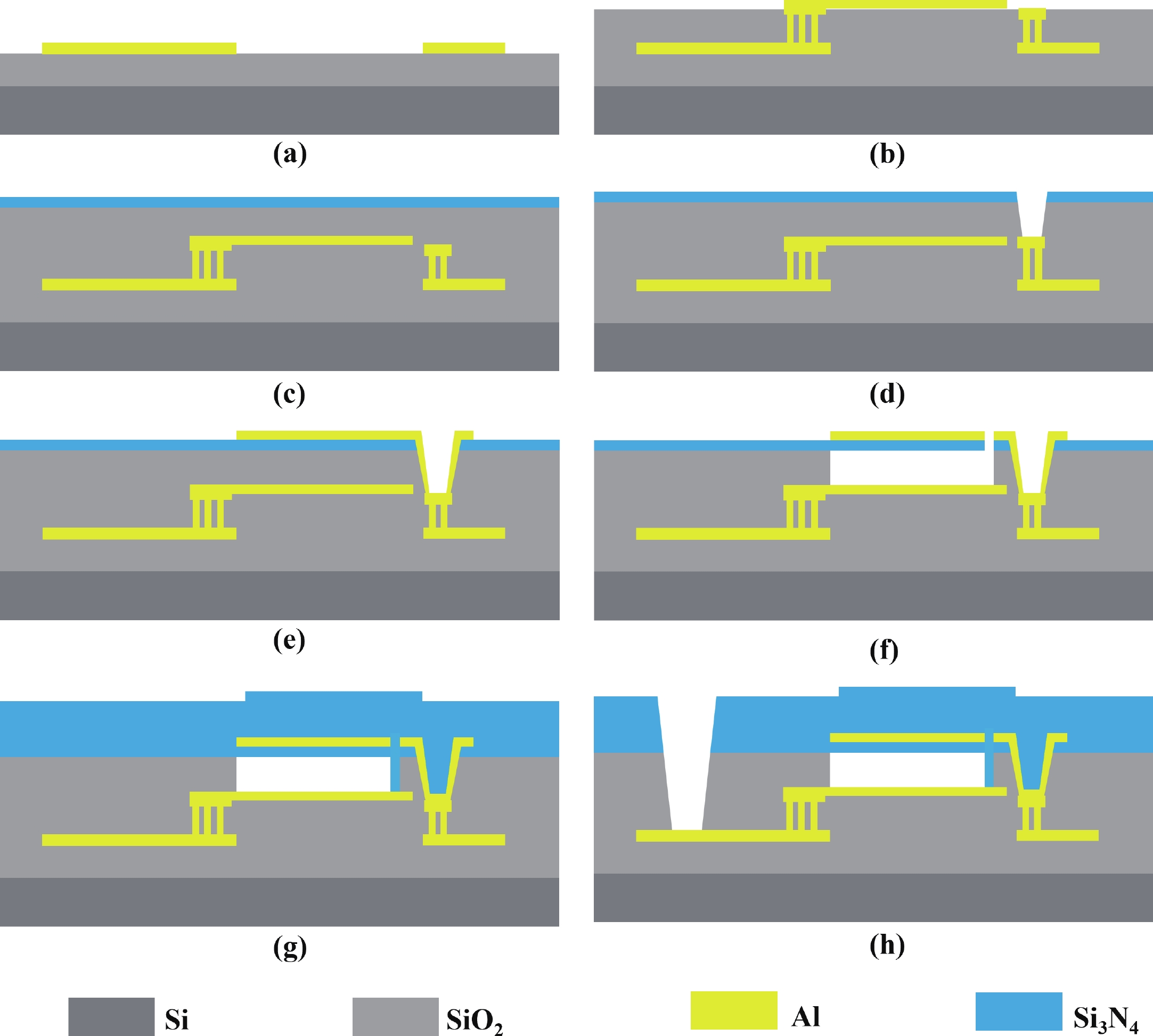
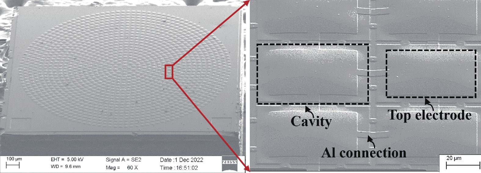
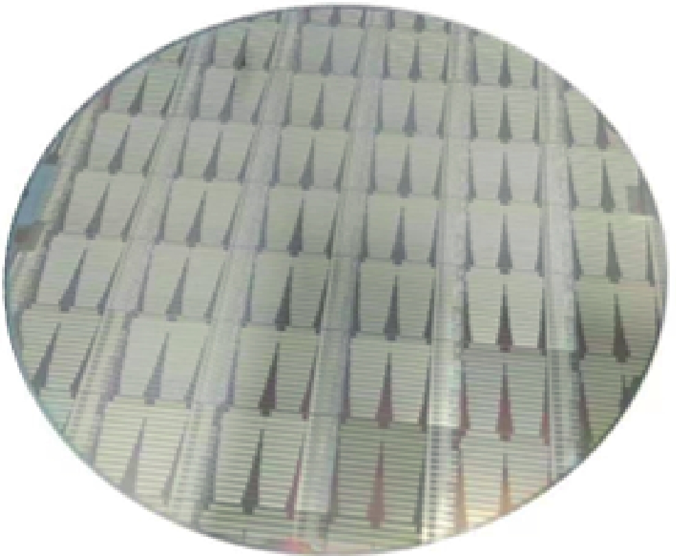
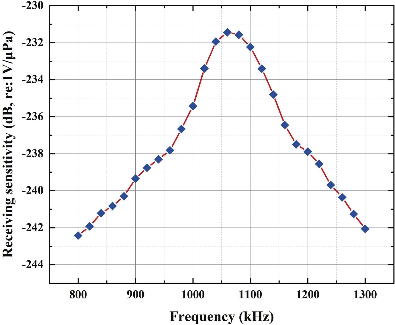
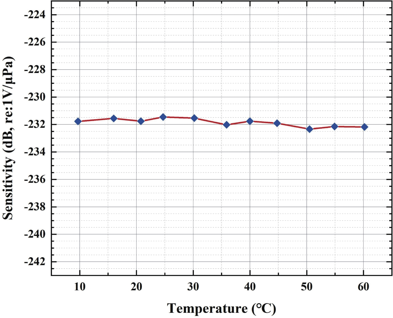
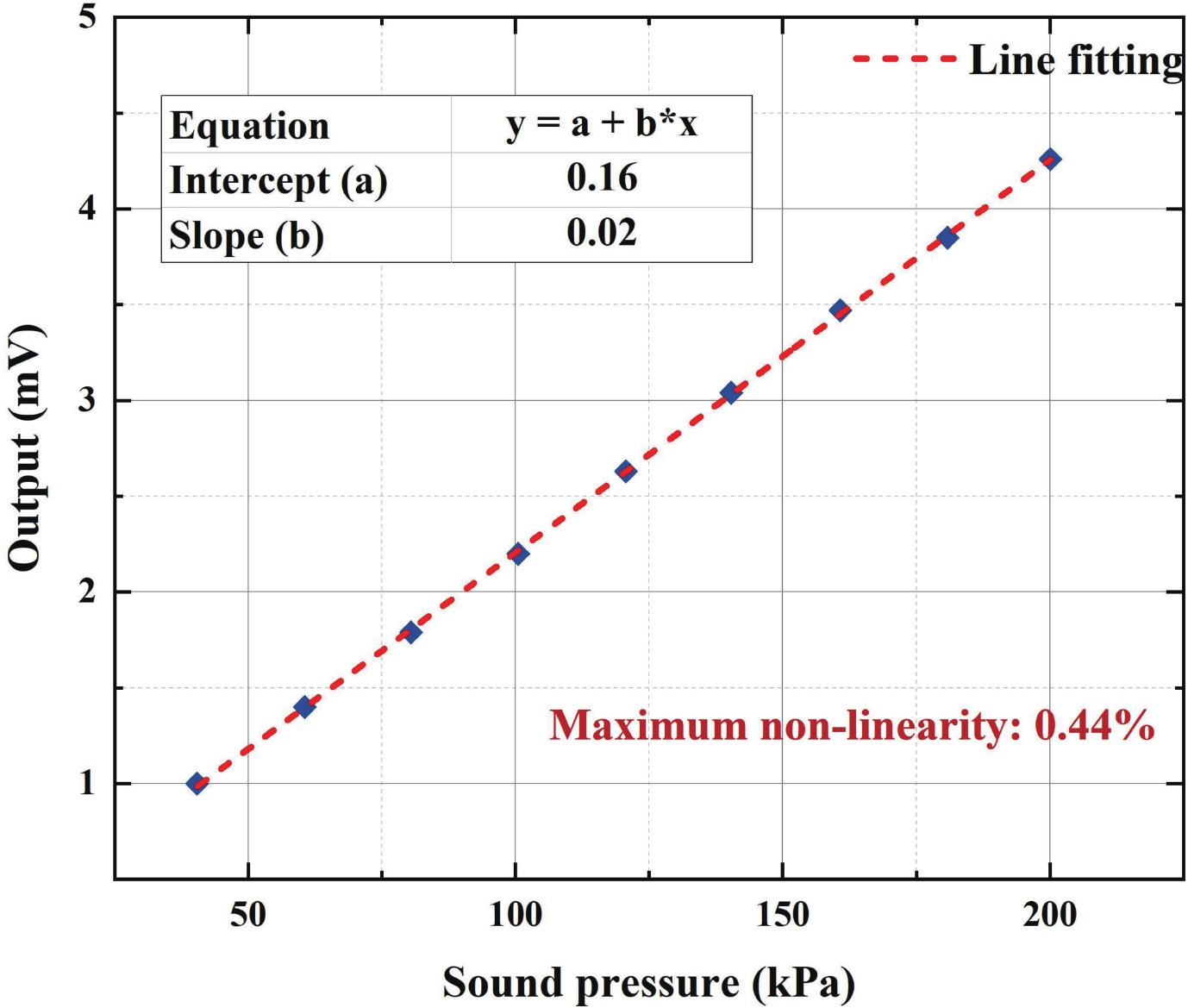
This paper presents the design, fabrication, packaging, and characterization of a high-performance CMUT array. The array, which features rectangular cells fabricated using a sacrificial release process, achieves a receiving sensitivity of −231.44 dB (re: 1 V/μPa) with a 40 dB gain. Notably, the CMUT array exhibits a minimal sensitivity variation of just 0.87 dB across a temperature range of 0 to 60 °C. Furthermore, the output voltage non-linearity at 1 kHz is approximately 0.44%. These test results demonstrate that the reception performance of the 67-element CMUT array is superior to that of commercial transducers. The high performance and compact design of this CMUT array underscore its significant commercial potential for hydrophone applications.
J. Semicond.
2024, 45(11): 112501 doi: 10.1088/1674-4926/24050015
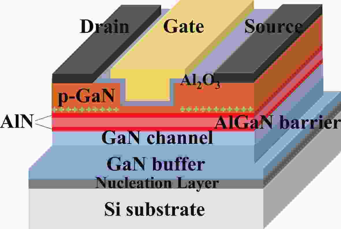
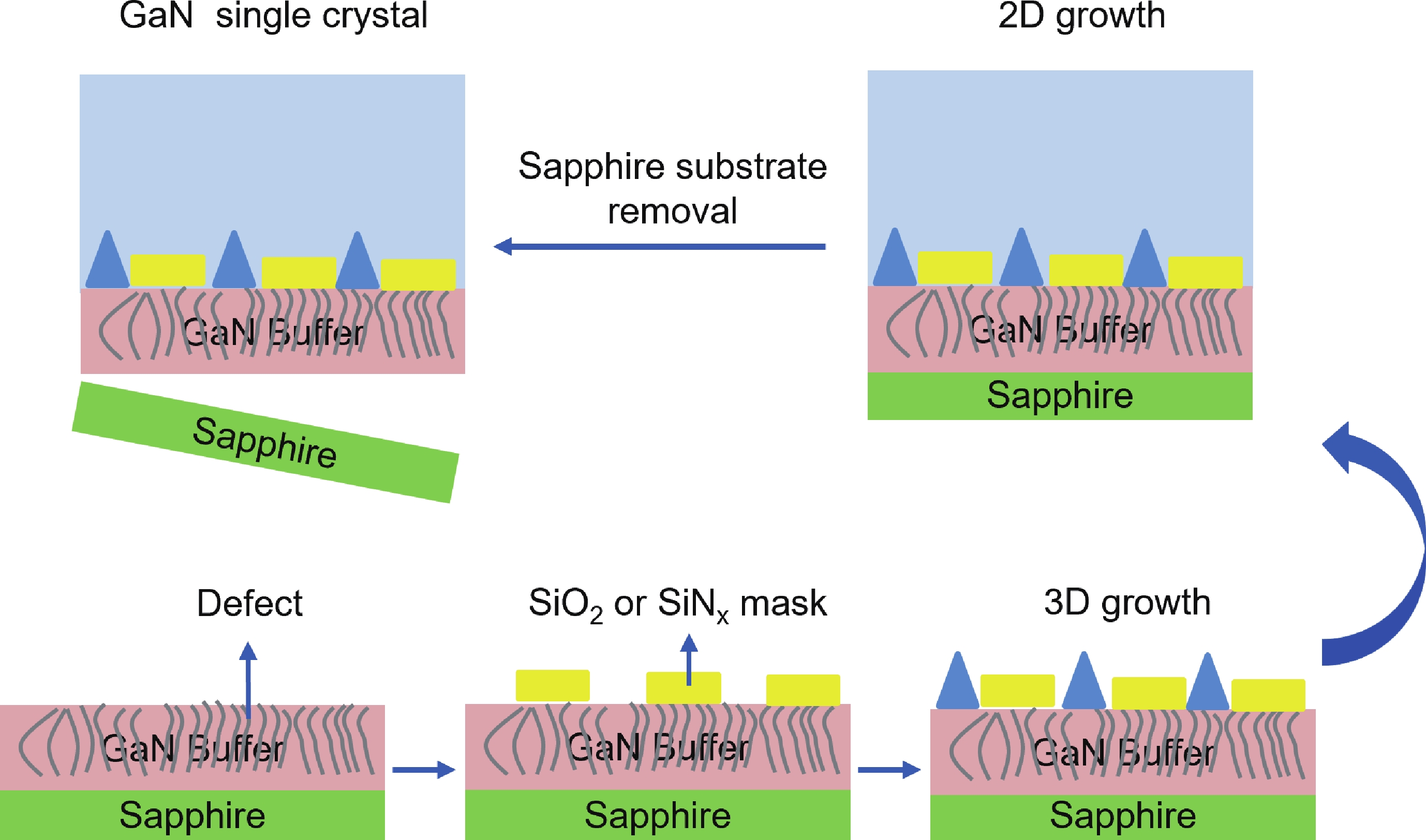
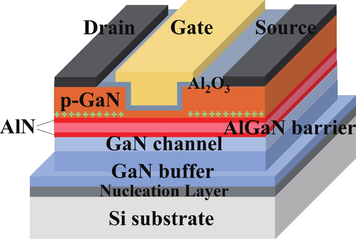
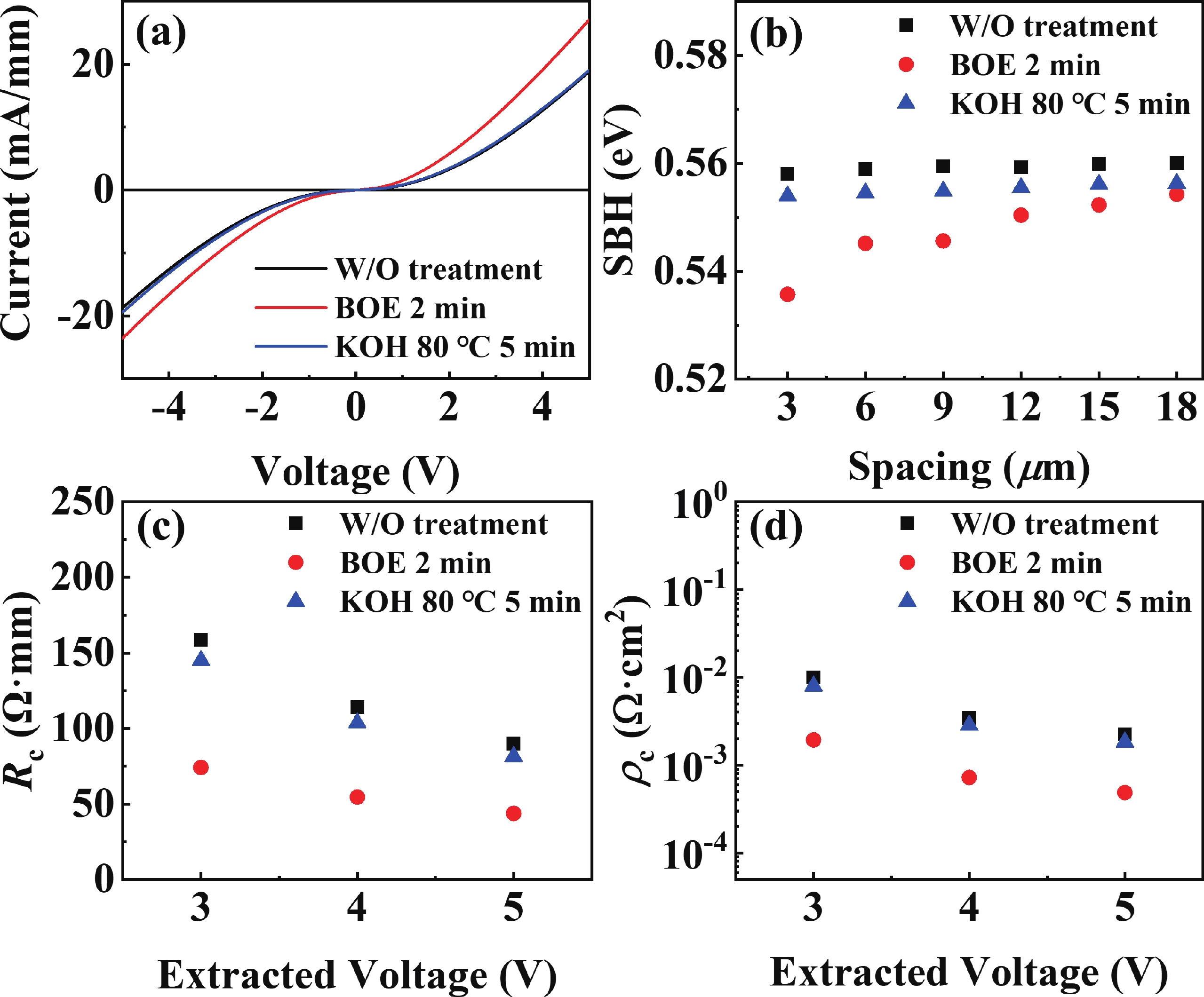
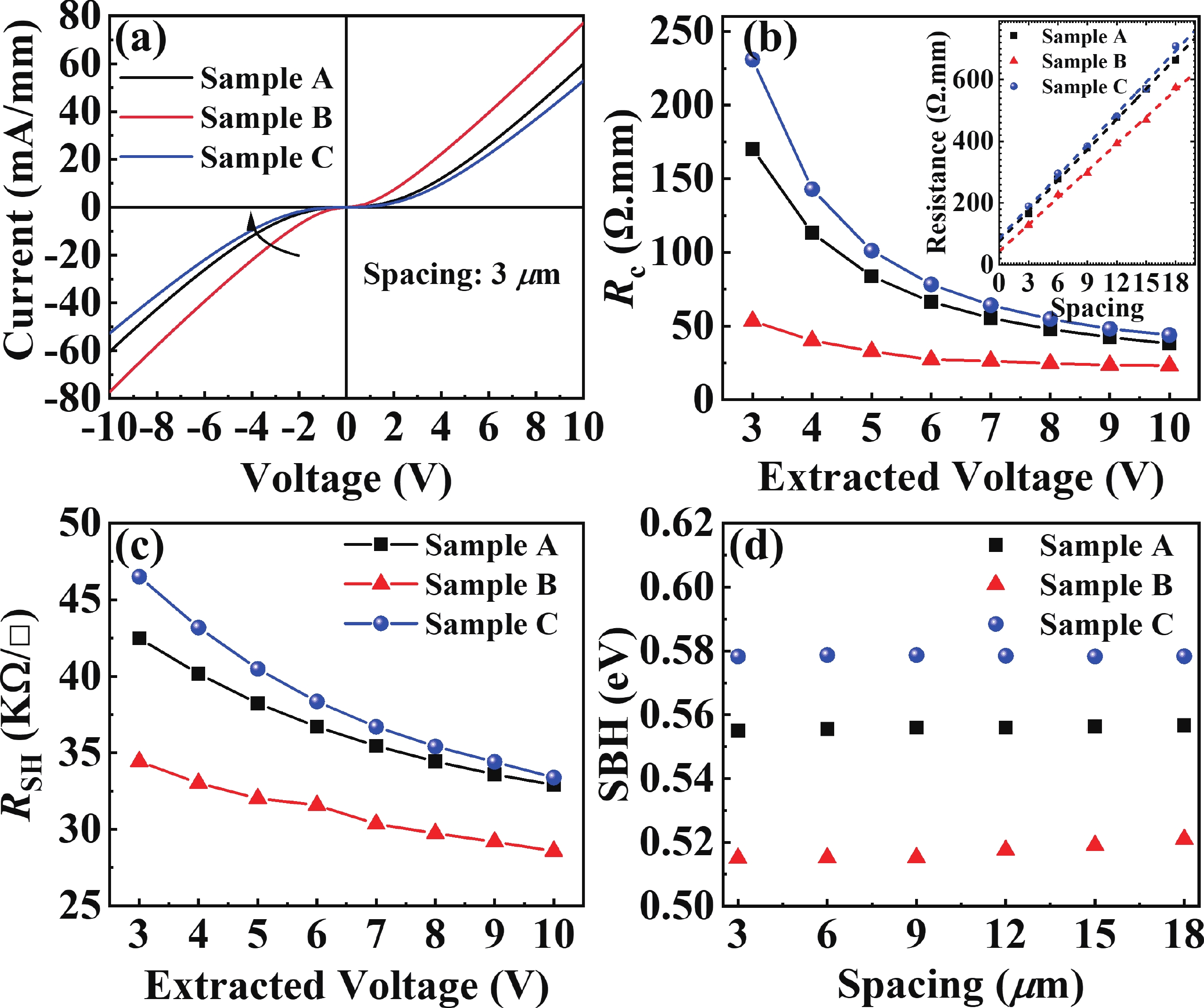
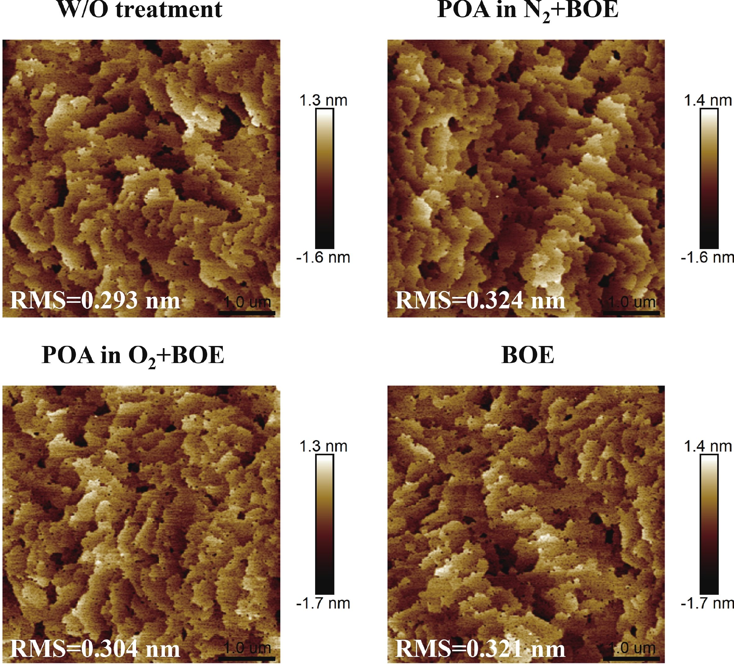
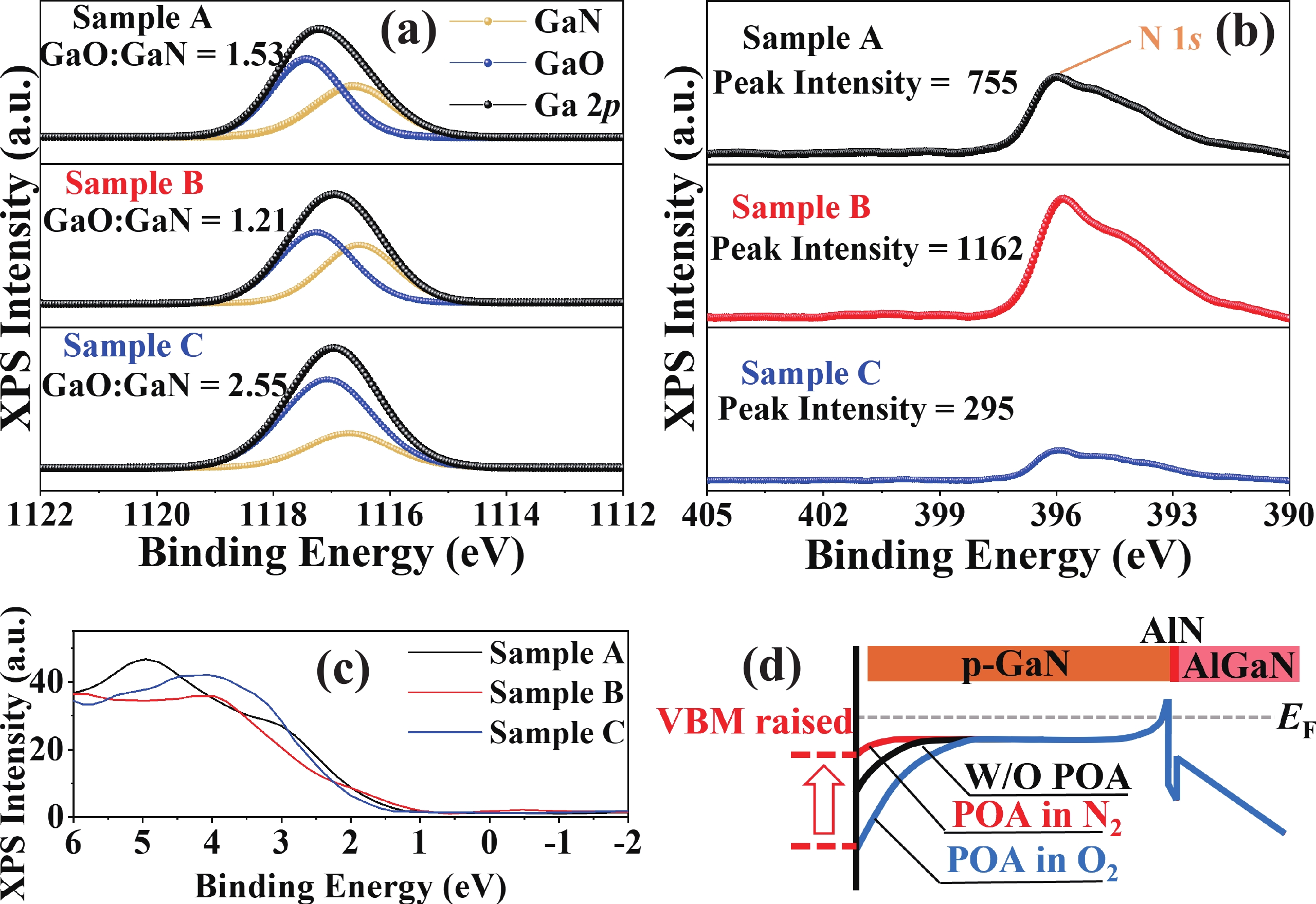
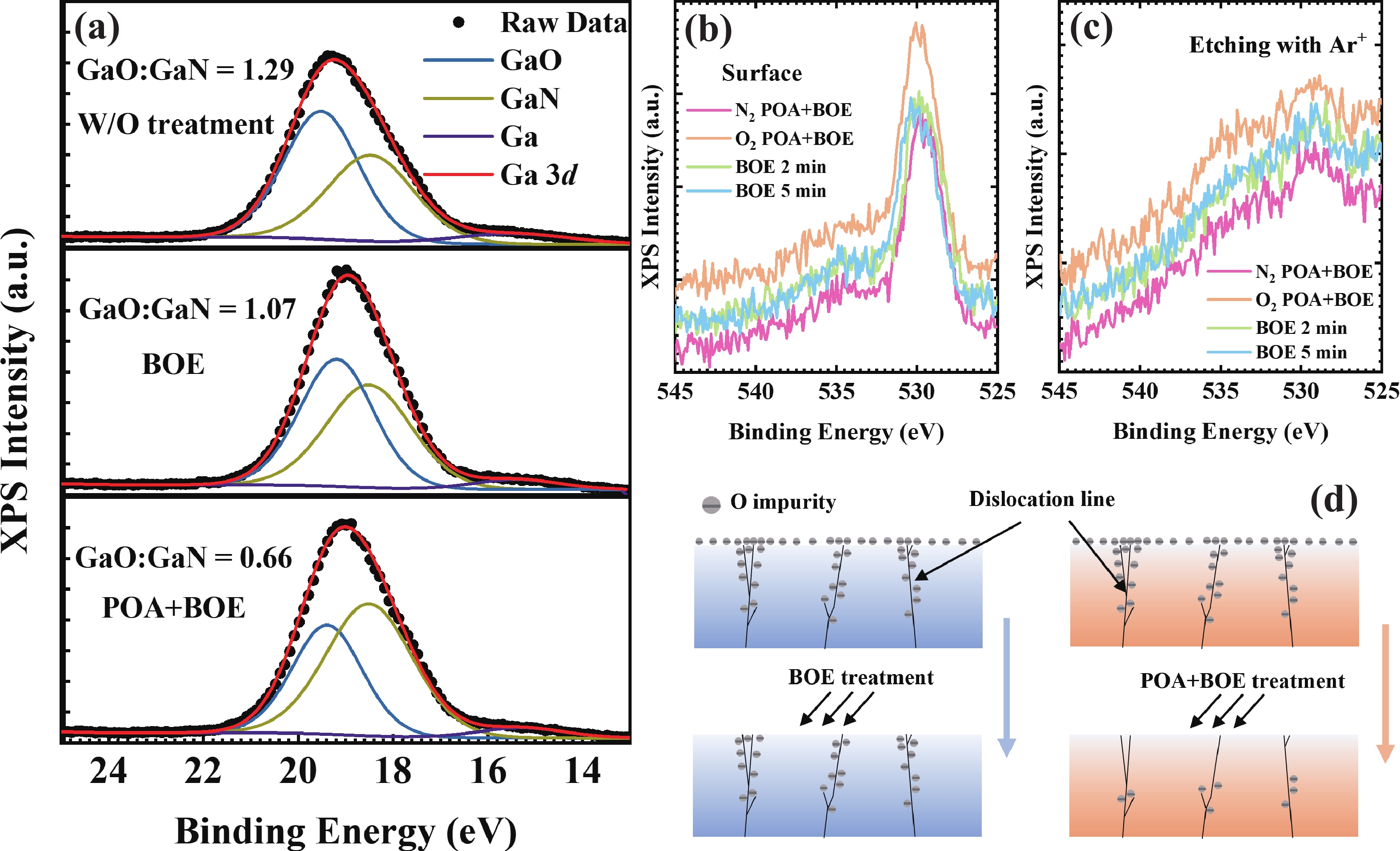
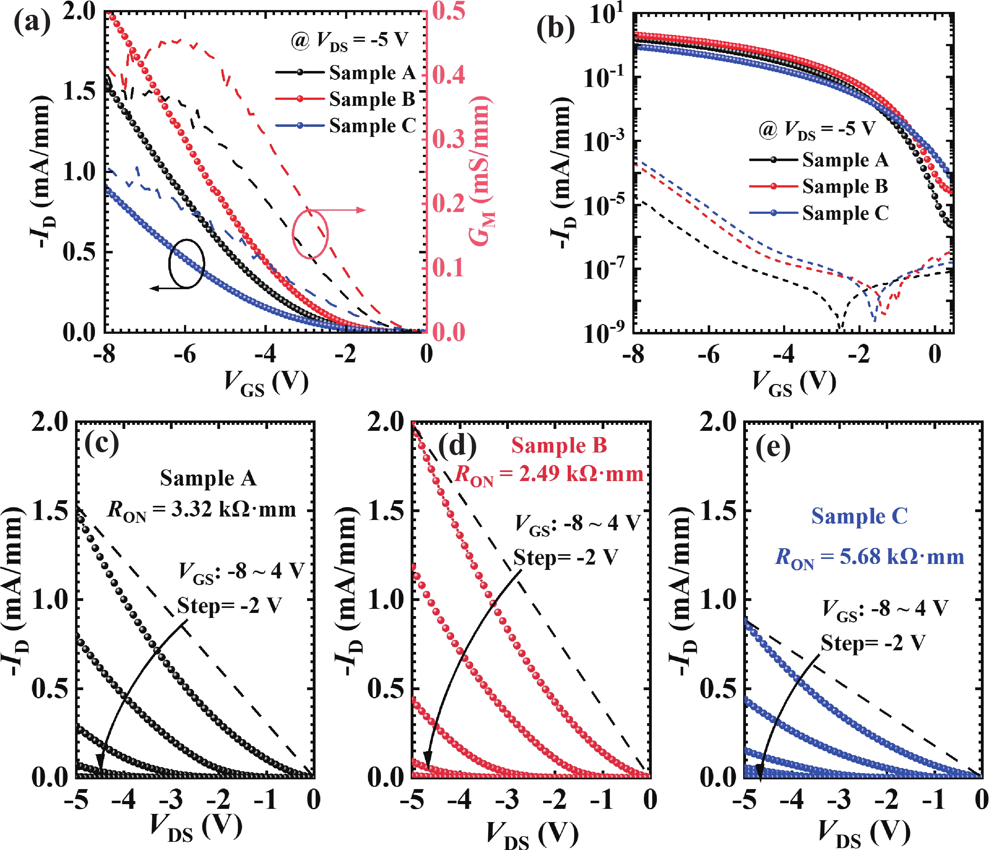
Pre-ohmic-annealing (POA) treatment of P-GaN/AlN/AlGaN epitaxy under N2 atmosphere was demonstrated to effectively achieve good p-type ohmic contact as well as decreased epitaxy sheet resistance. Ohmic contact resistance (Rc) extracted by transfer length method reduced from 38 to 23 Ω·mm with alleviated contact barrier height from 0.55 to 0.51 eV after POA treatment. X-ray photoelectron spectroscopy and Hall measurement confirmed that POA treatment was able to reduce surface state density and improve the hole concentration of p-GaN. Due to the decreased Rc and improved two-dimensional hole gas (2DHG) density, an outstanding-performance GaN E-mode p-channel MOSFET was successfully realized.
J. Semicond.
2024, 45(11): 112502 doi: 10.1088/1674-4926/24050027
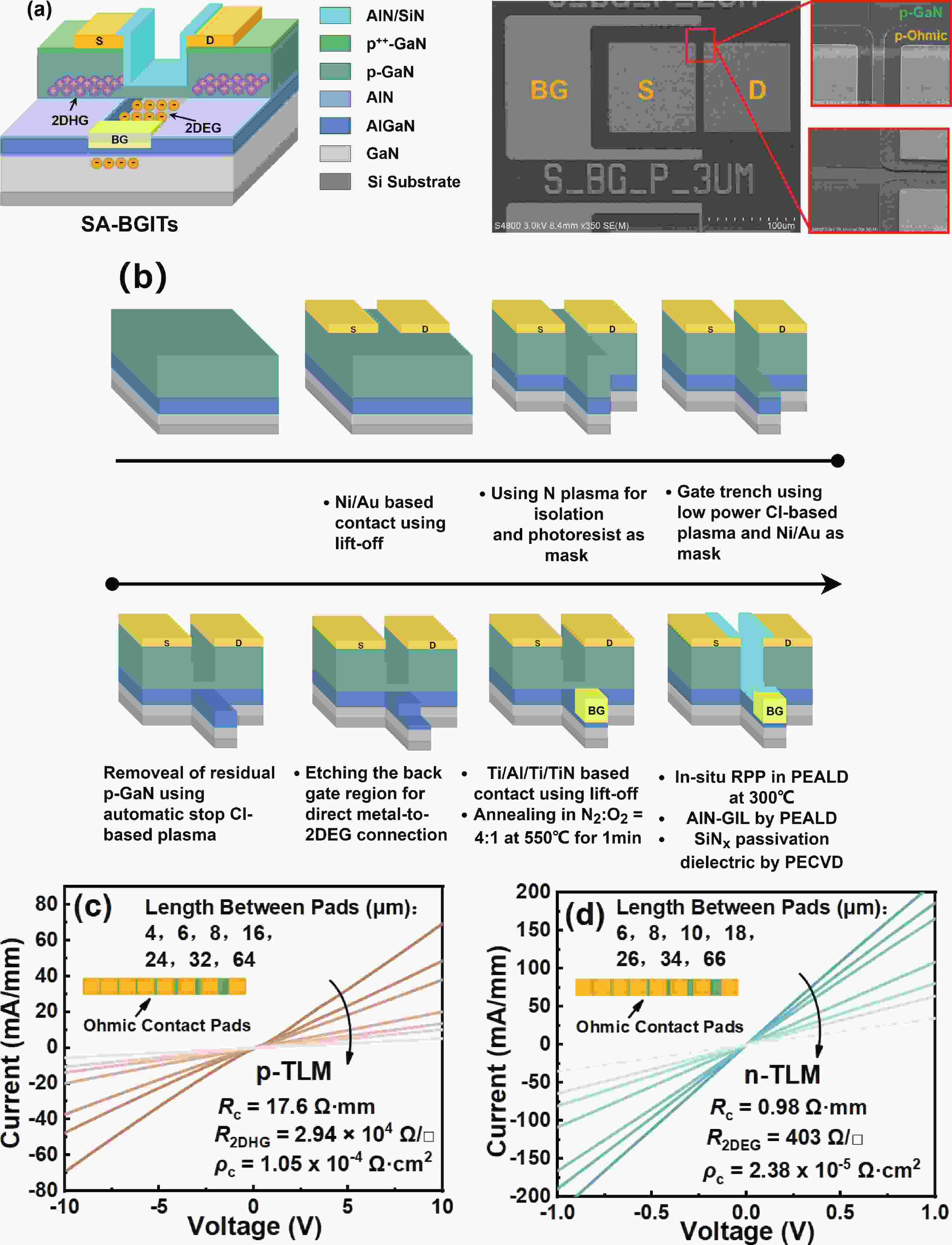
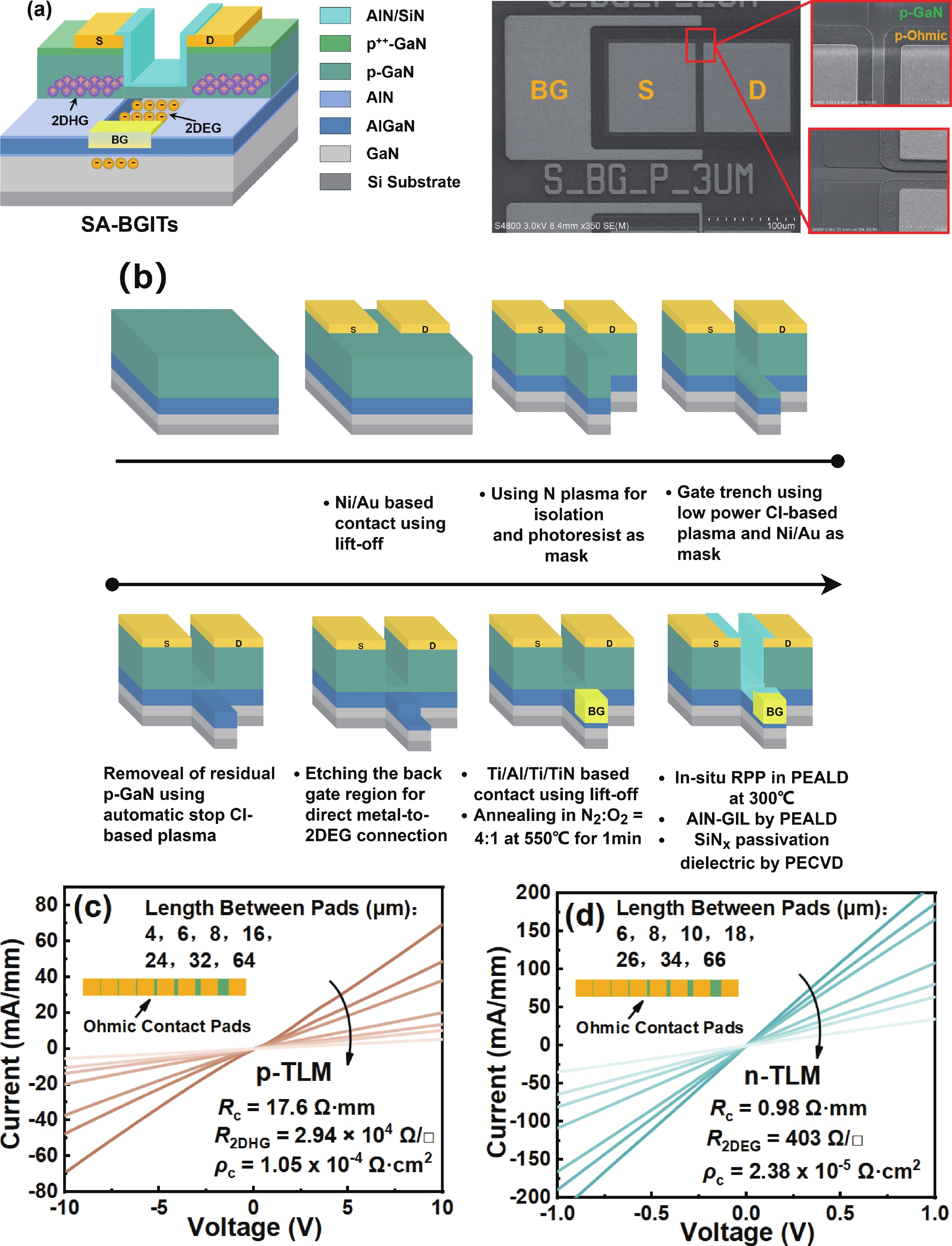
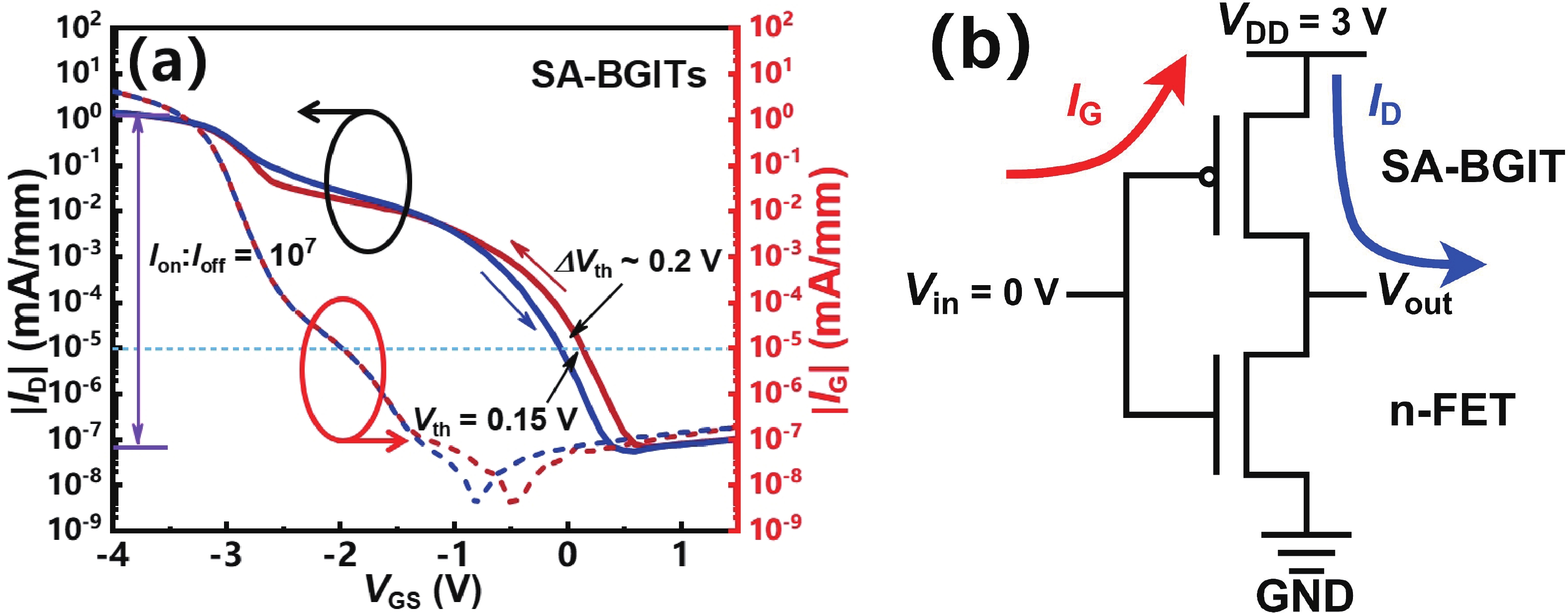
In this study, we present the development of self-aligned p-channel GaN back gate injection transistors (SA-BGITs) that exhibit a high ON-state current. This achievement is primarily attributed to the conductivity modulation effect of the 2-D electron gas (2DEG, the back gate) beneath the 2-D hole gas (2DHG) channel. SA-BGITs with a gate length of 1 μm have achieved an impressive peak drain current (ID,MAX) of 9.9 mA/mm. The fabricated SA-BGITs also possess a threshold voltage of 0.15 V, an exceptionally minimal threshold hysteresis of 0.2 V, a high switching ratio of 107, and a reduced ON-resistance (RON) of 548 Ω·mm. Additionally, the SA-BGITs exhibit a steep sub-threshold swing (SS) of 173 mV/dec, further highlighting their suitability for integration into GaN logic circuits.
J. Semicond.
2024, 45(11): 112503 doi: 10.1088/1674-4926/24050011
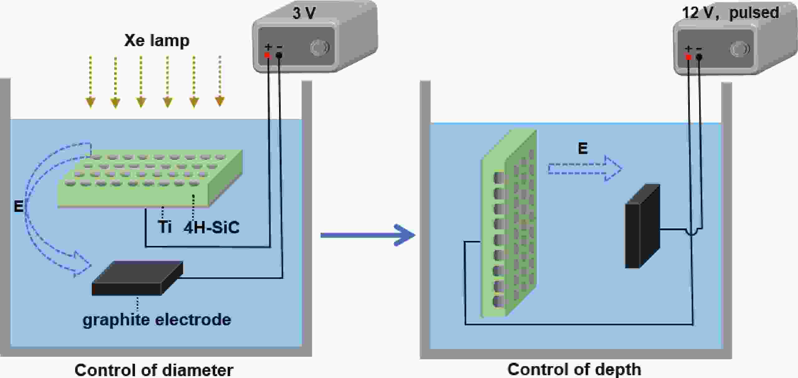
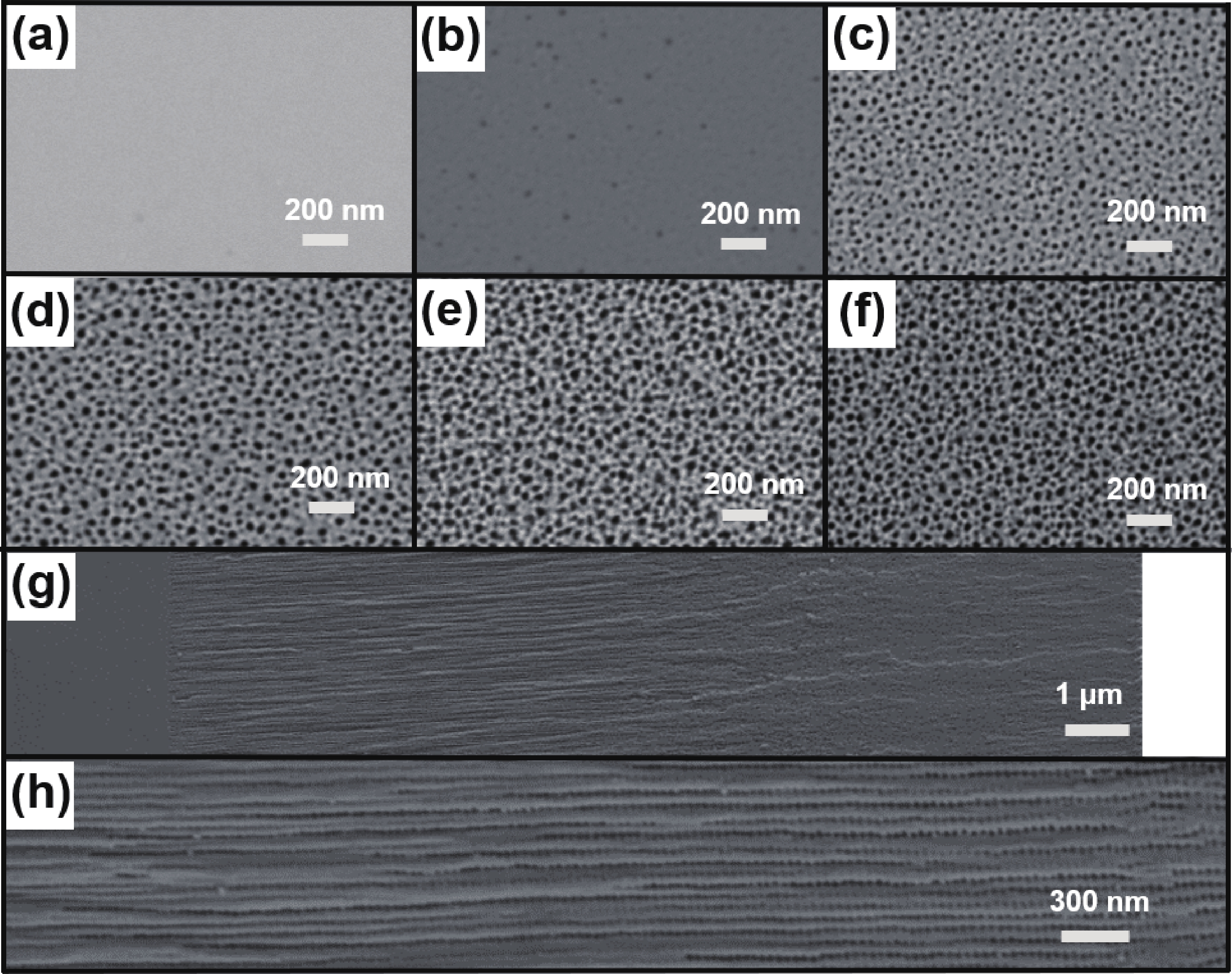
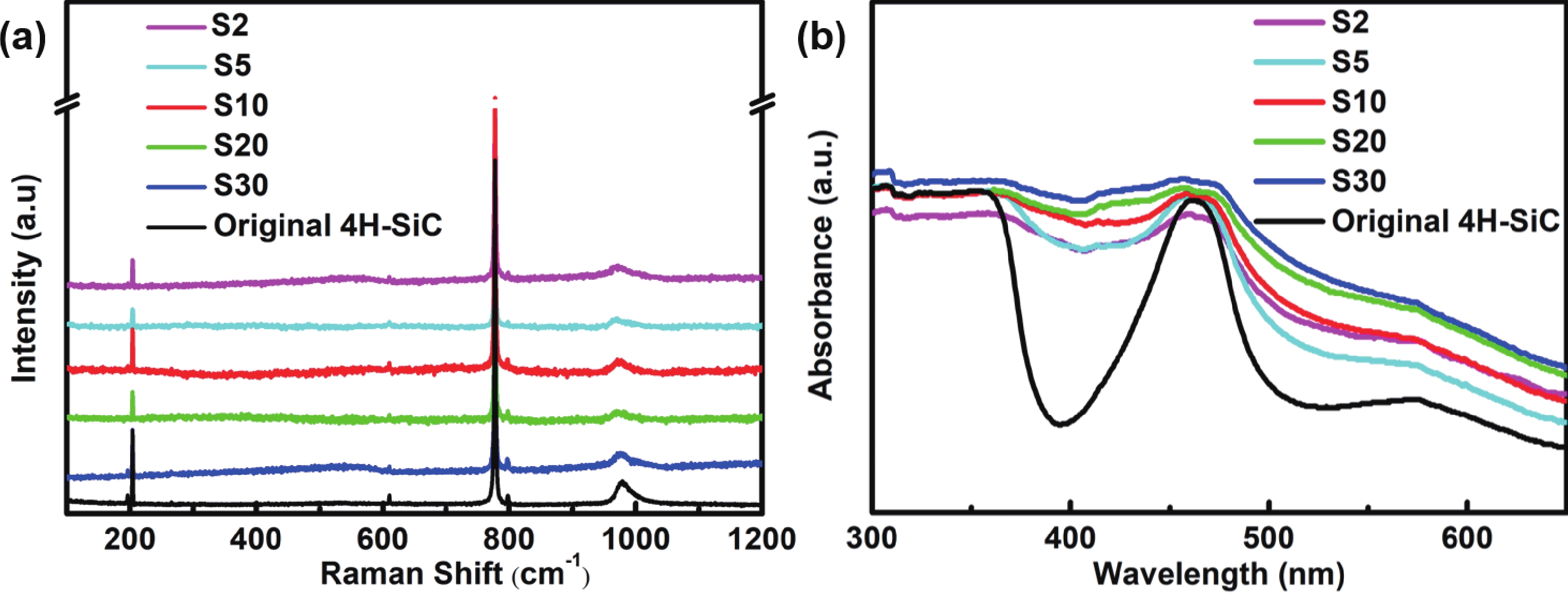
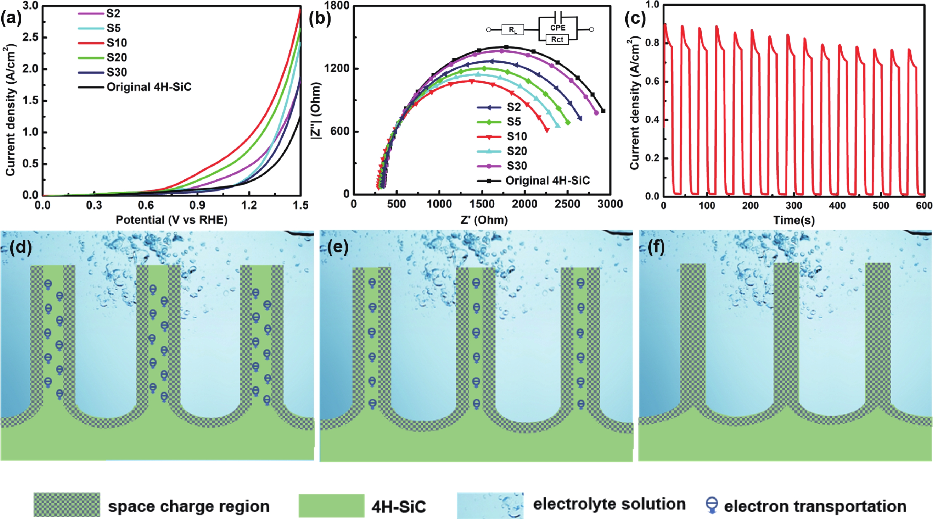
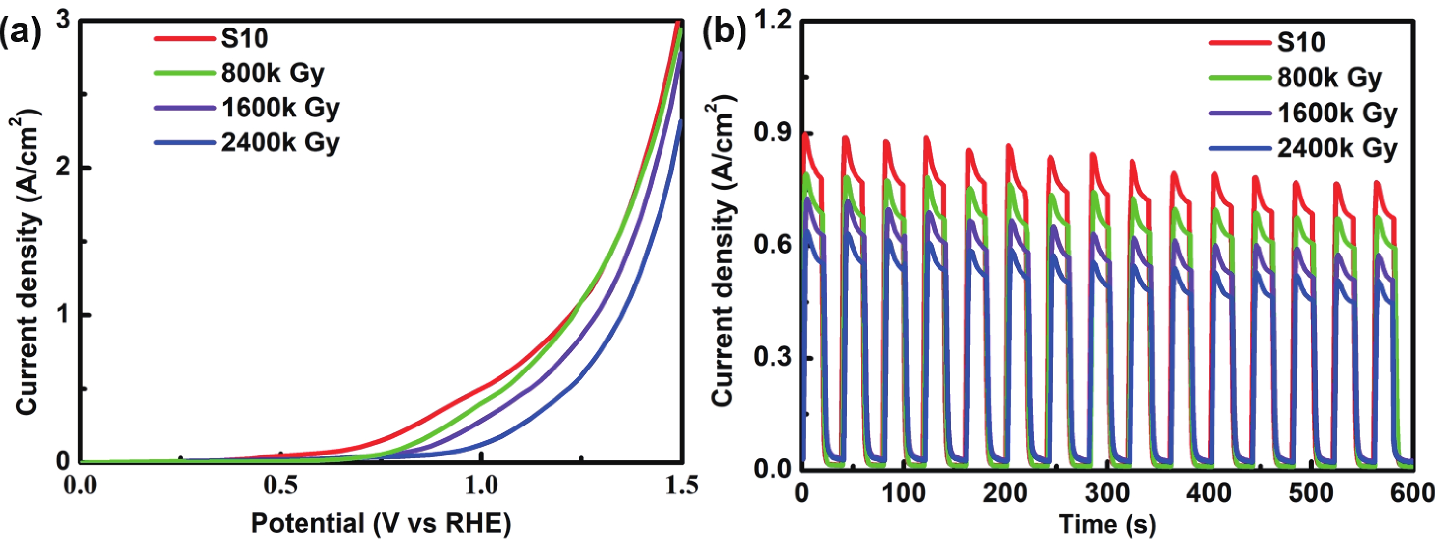
4H silicon carbide (4H-SiC) has gained a great success in high-power electronics, owing to its advantages of wide bandgap, high breakdown electric field strength, high carrier mobility, and high thermal conductivity. Considering the high carrier mobility and high stability of 4H-SiC, 4H-SiC has great potential in the field of photoelectrochemical (PEC) water splitting. In this work, we demonstrate the irradiation-resistant PEC water splitting based on nanoporous 4H-SiC arrays. A new two-step anodizing approach is adopted to prepare 4H-SiC nanoporous arrays with different porosity, that is, a constant low-voltage etching followed by a pulsed high-voltage etching. The constant-voltage etching and pulsed-voltage etching are adopted to control the diameter of the nanopores and the depth of the nanoporous arrays, respectively. It is found that the nanoporous arrays with medium porosity has the highest PEC current, because of the enhanced light absorption and the optimized transportation of charge carriers along the walls of the nanoporous arrays. The performance of the PEC water splitting of the nanoporous arrays is stable after the electron irradiation with the dose of 800 and 1600 kGy, which indicates that 4H-SiC nanoporous arrays has great potential in the PEC water splitting under harsh environments.
J. Semicond.
2024, 45(11): 112701 doi: 10.1088/1674-4926/24060019
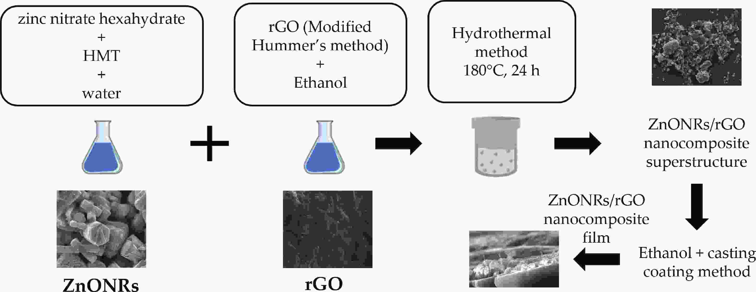
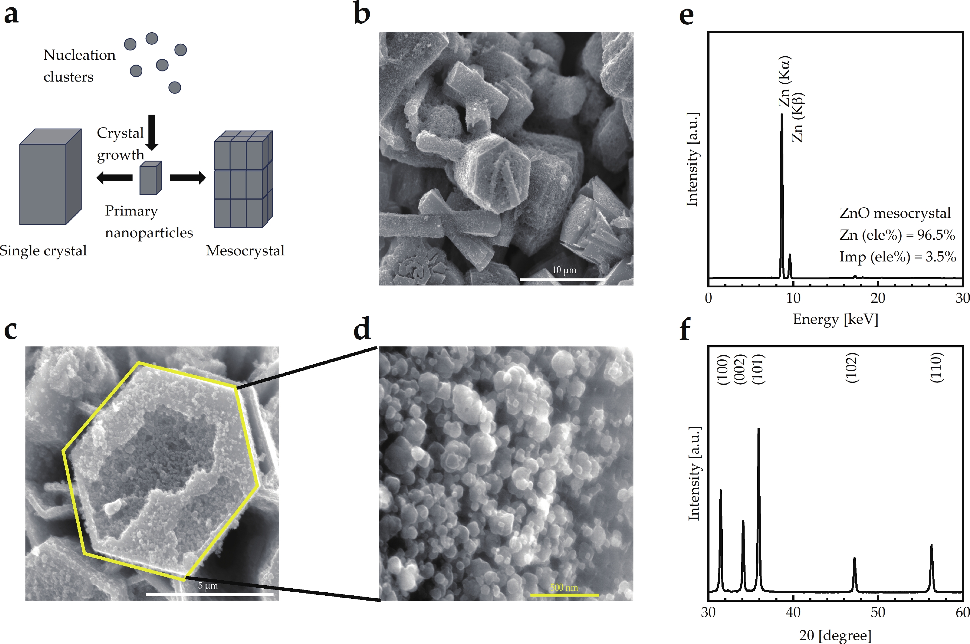
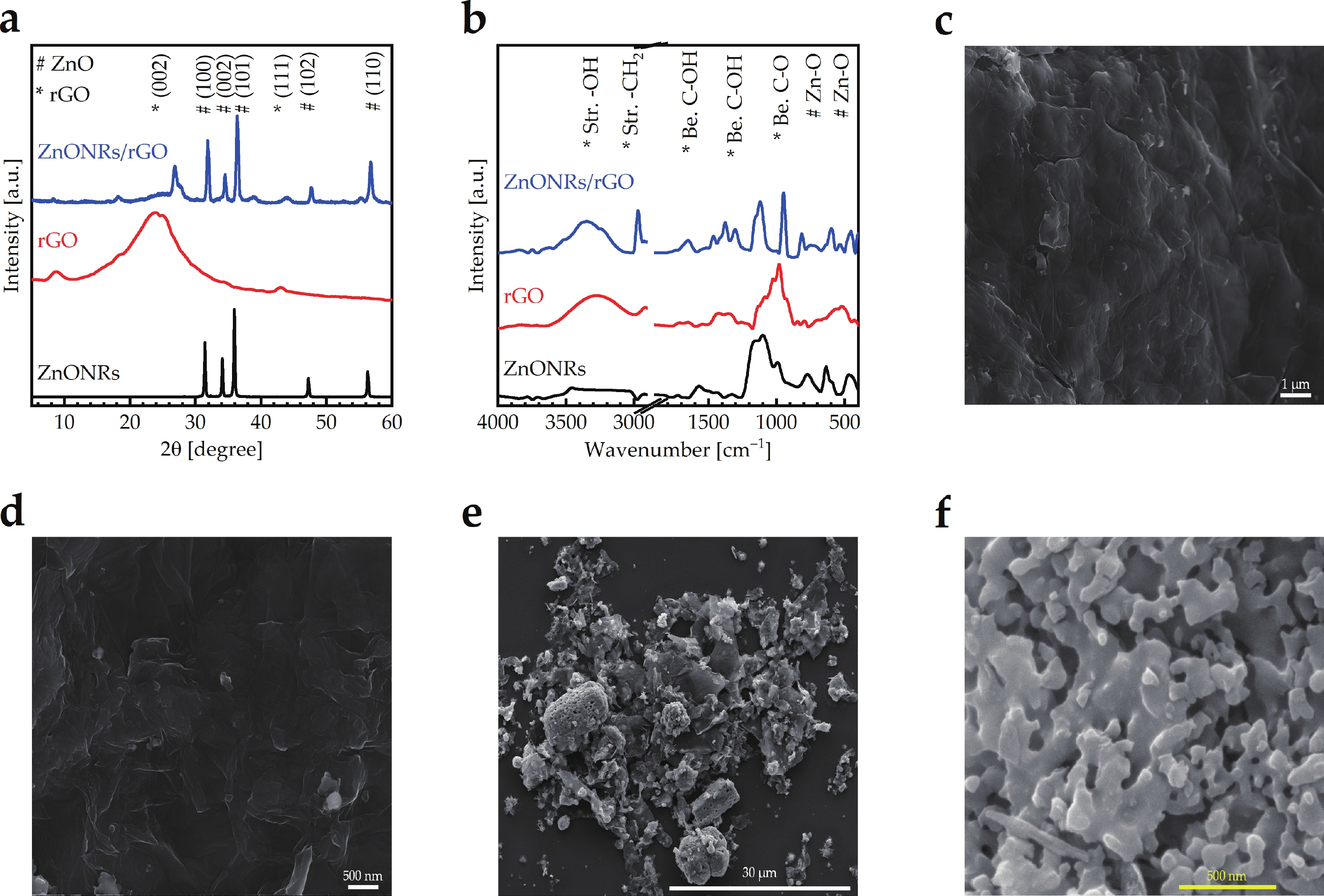
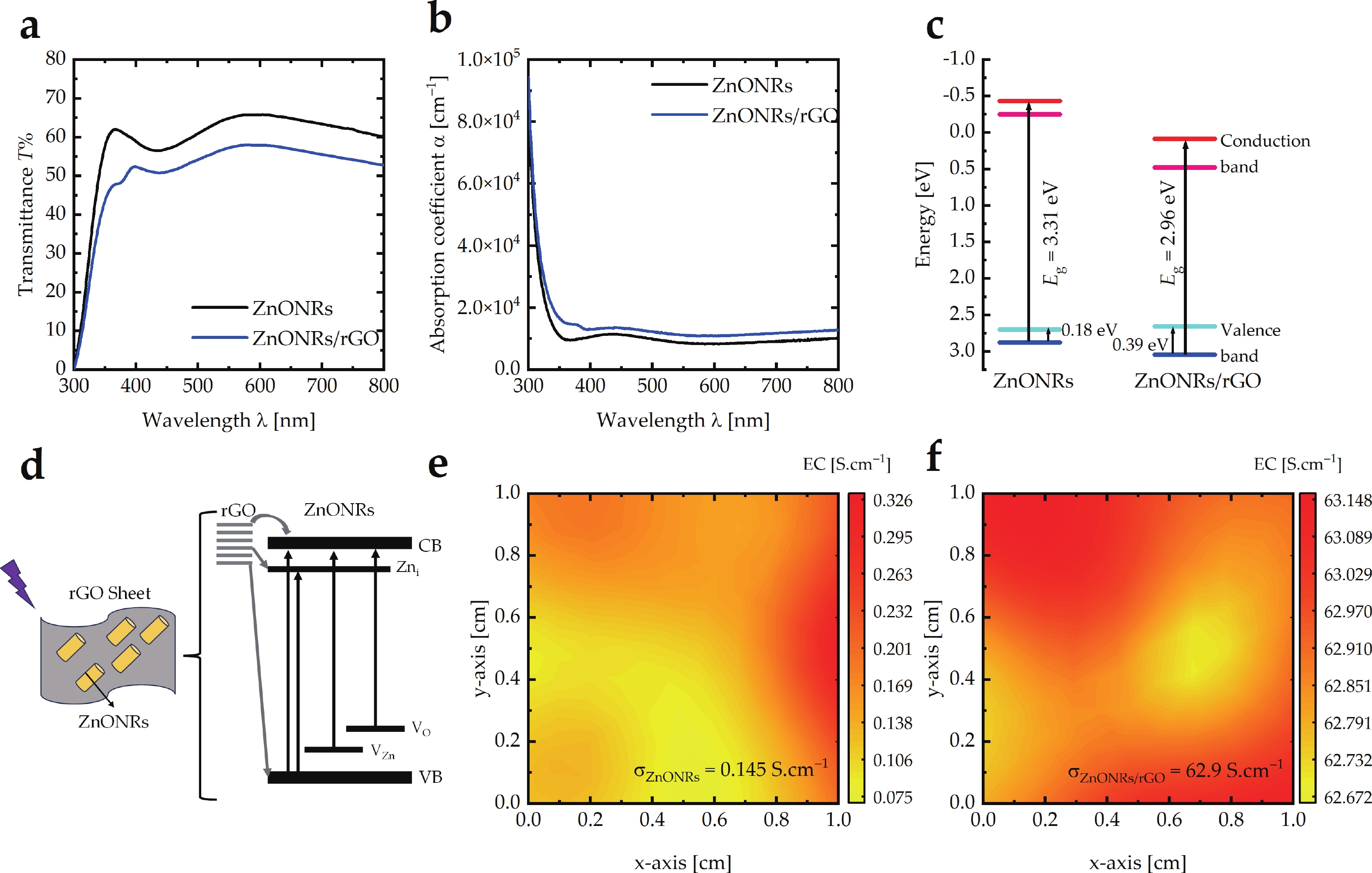
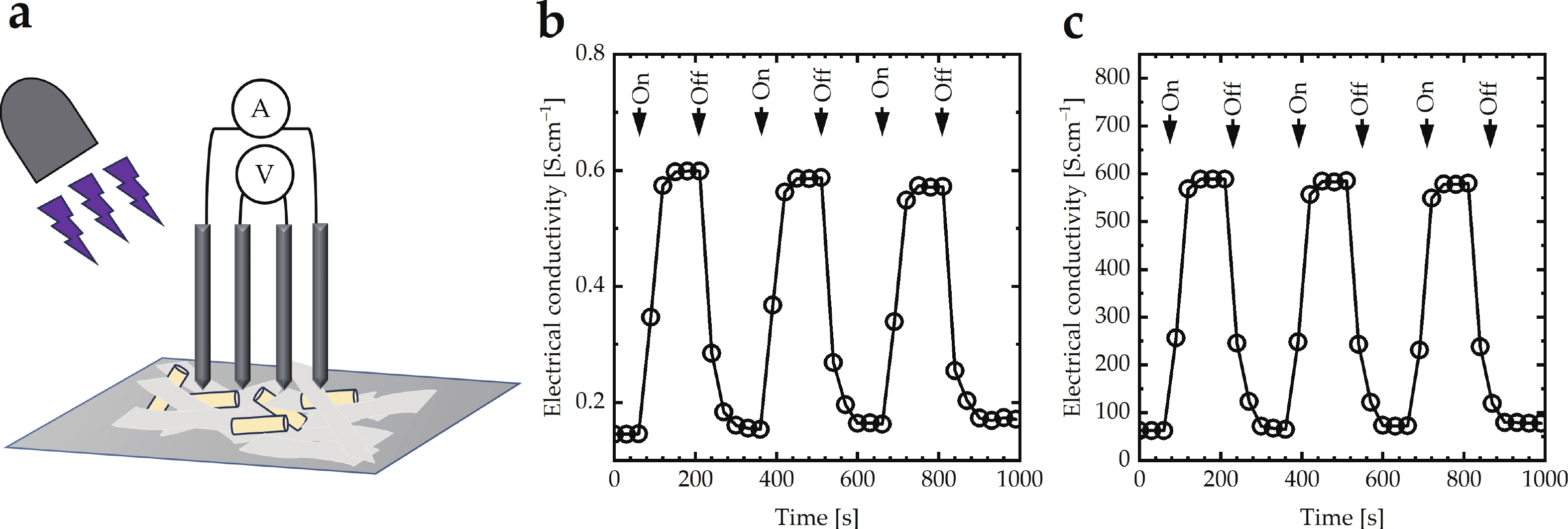
Metal oxide mesocrystals are the alignment of metal oxide nanoparticles building blocks into the ordered superstructure, which have potentially tunable optical, electronic, and electrical properties suitable for practical applications. Herein, we report an effective method for synthesizing mesocrystal zinc oxide nanorods (ZnONRs). The crystal, surface, and internal structures of the zinc oxide mesocrystals were fully characterized. Mesocrystal zinc oxide nanorods/reduced graphene oxide (ZnONRs/rGO) nanocomposite superstructure were synthesized also using the hydrothermal method. The crystal, surface, chemical, and internal structures of the ZnONRs/rGO nanocomposite superstructure were also fully characterized. The optical absorption coefficient, bandgap energy, band structure, and electrical conductivity of the ZnONRs/rGO nanocomposite superstructure were investigated to understand its optoelectronic and electrical properties. Finally, the photoconductivity of the ZnONRs/rGO nanocomposite superstructure was explored to find the possibilities of using this nanocomposite superstructure for ultraviolet (UV) photodetection applications. Finally, we concluded that the ZnONRs/rGO nanocomposite superstructure has high UV sensitivity and is suitable for UV detector applications.
J. Semicond.
2024, 45(11): 112801 doi: 10.1088/1674-4926/24060032
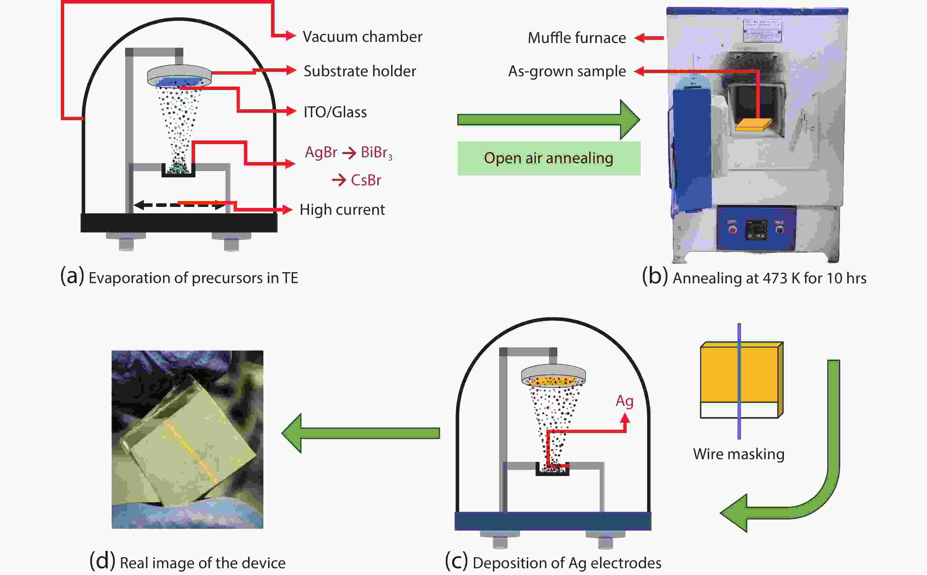
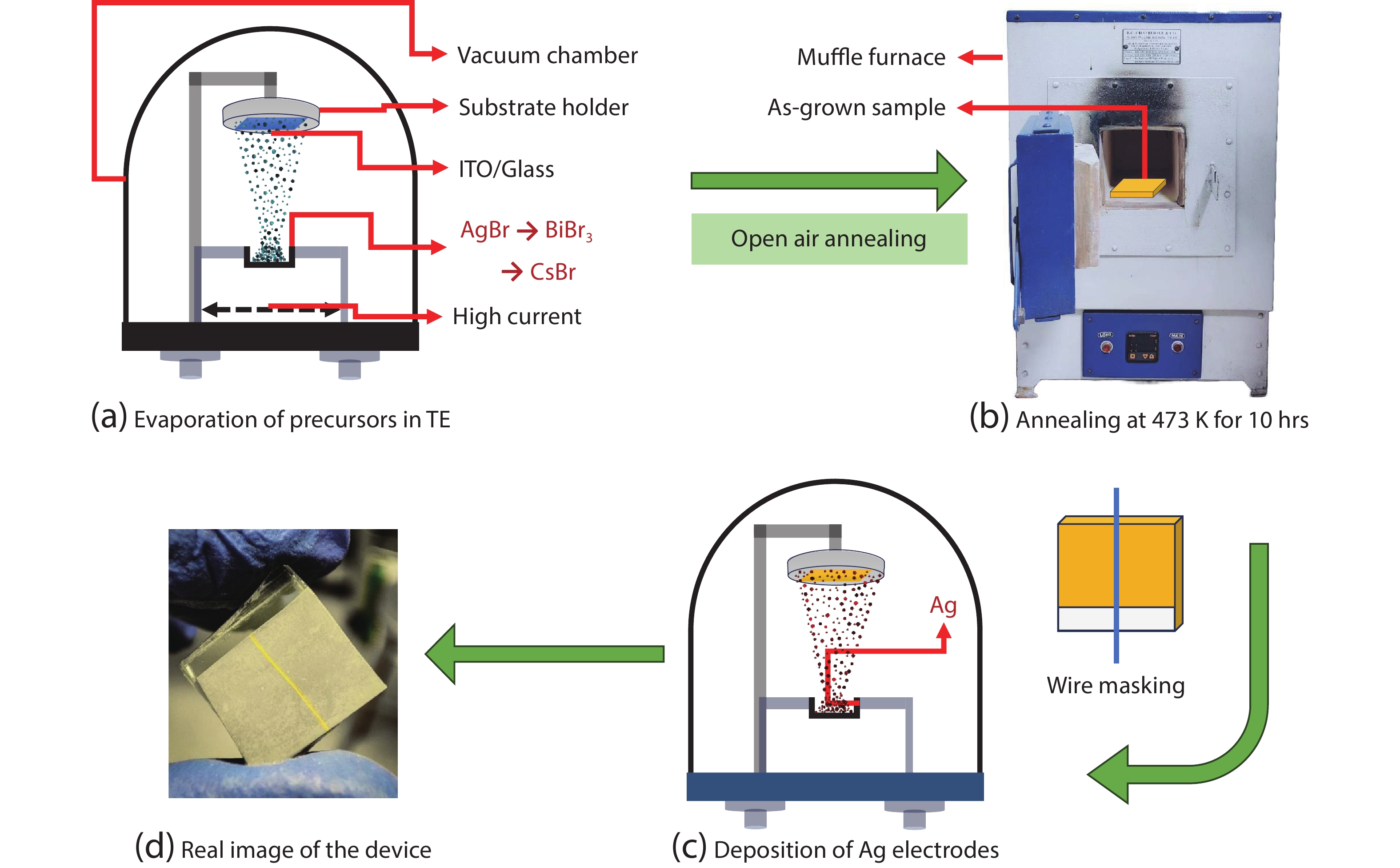
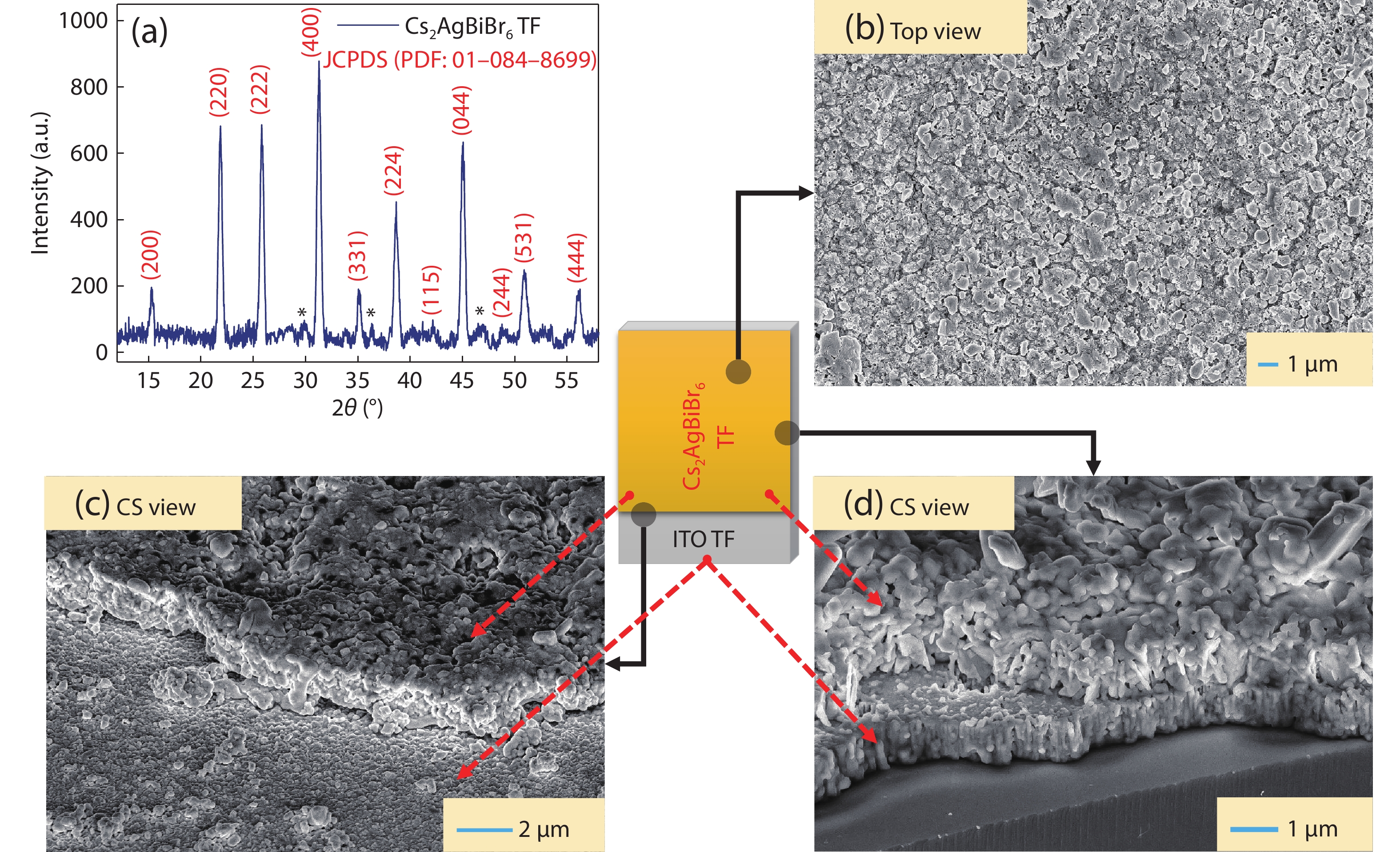
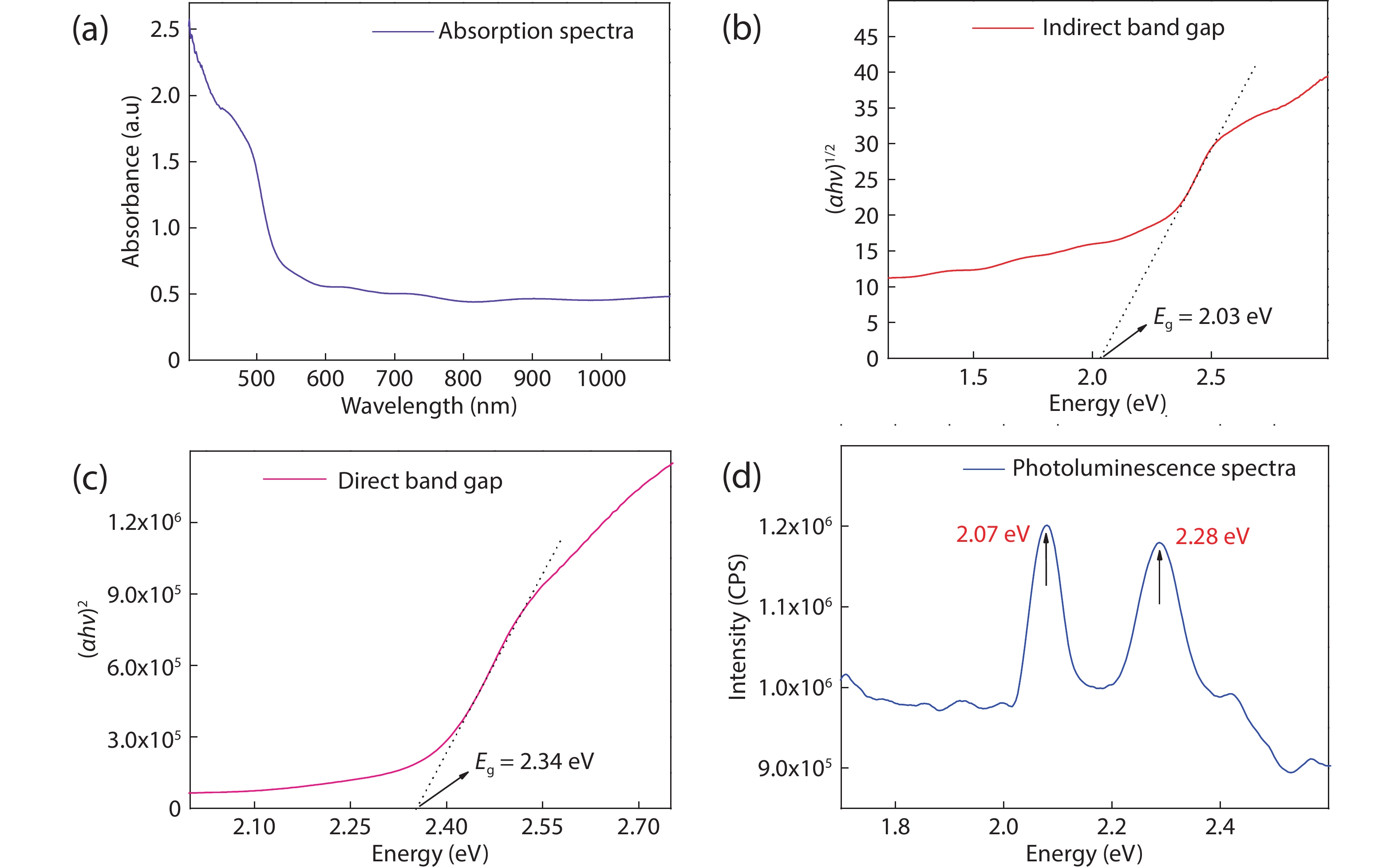
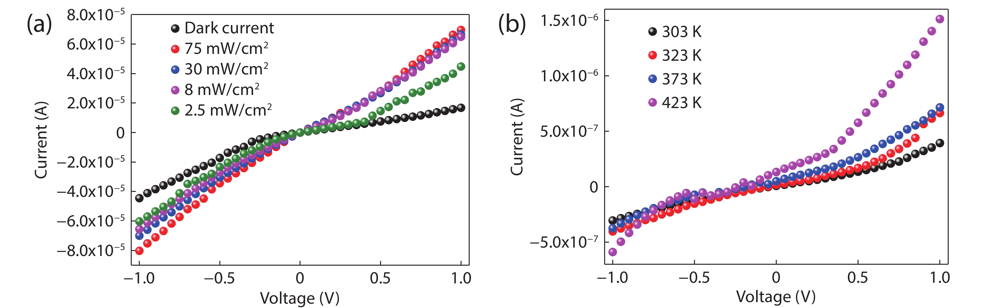
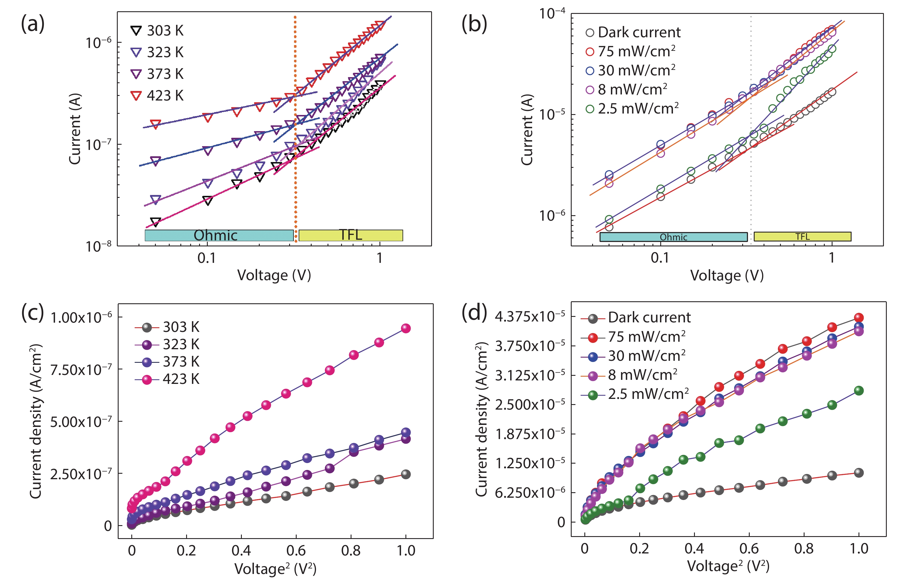
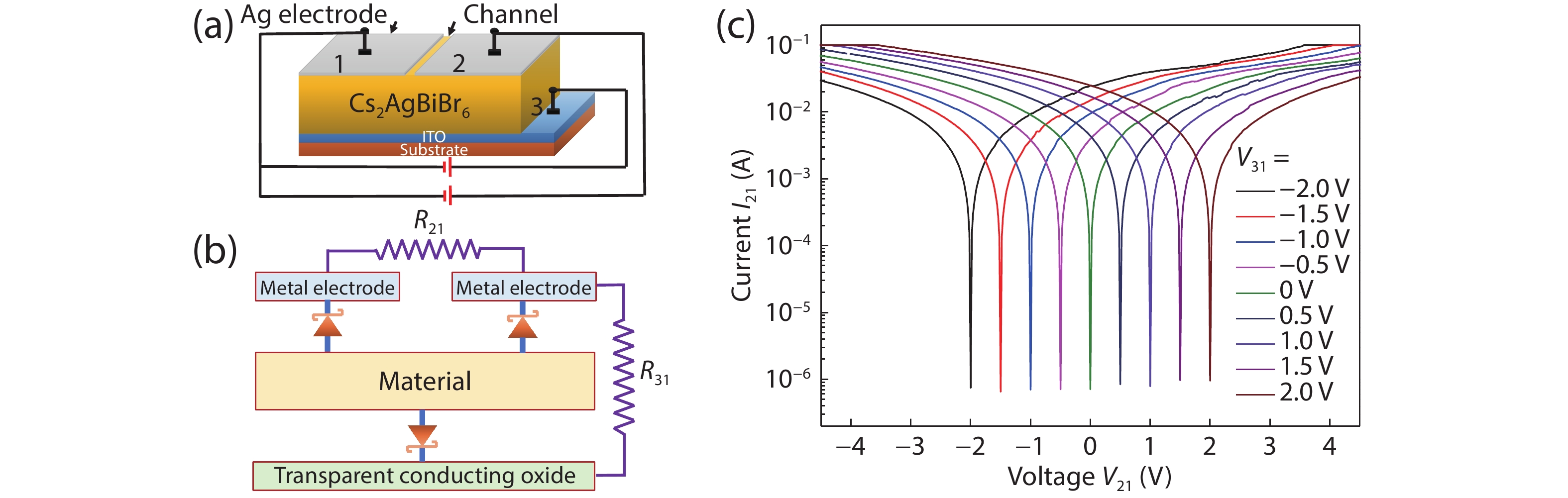
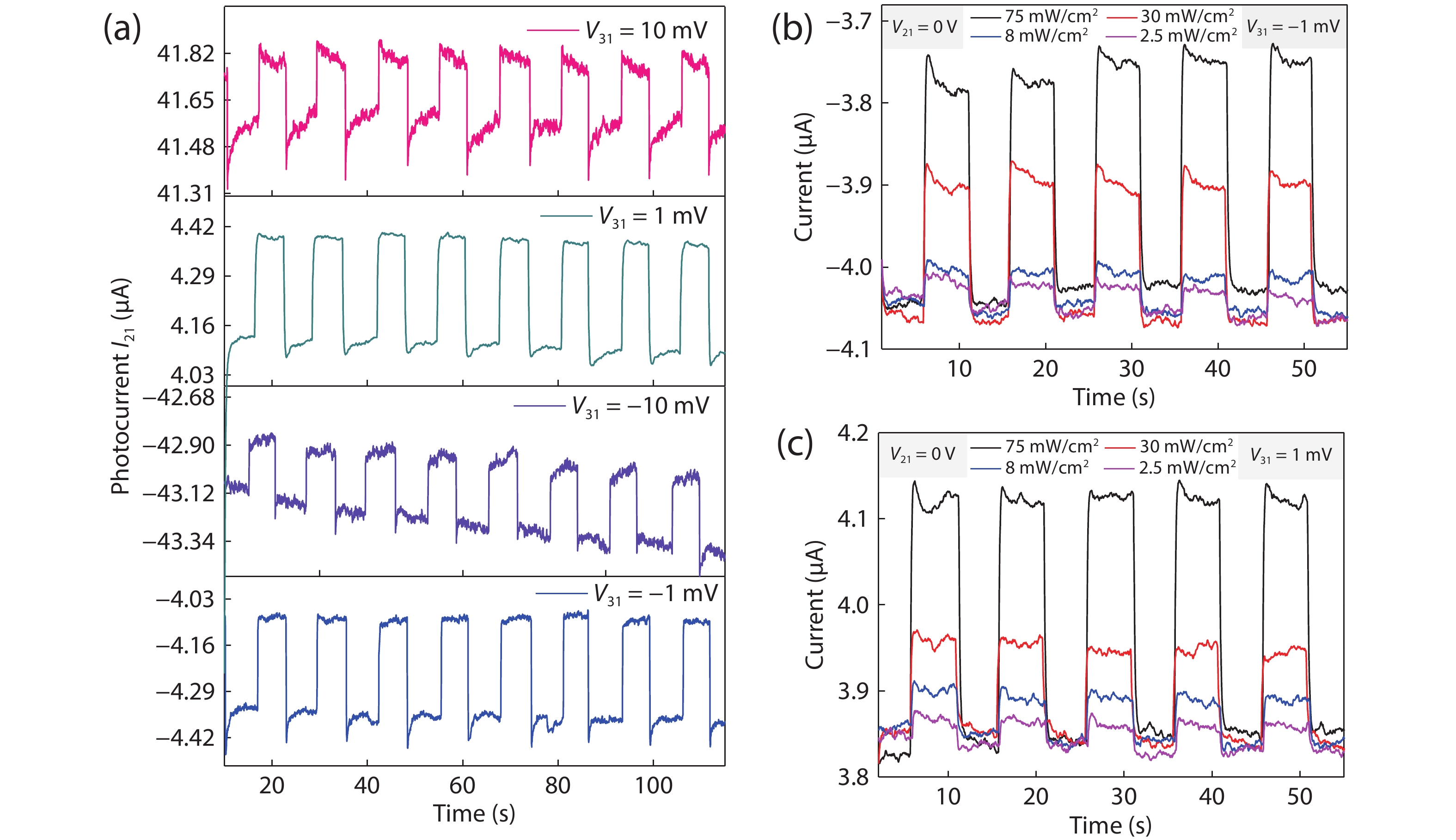
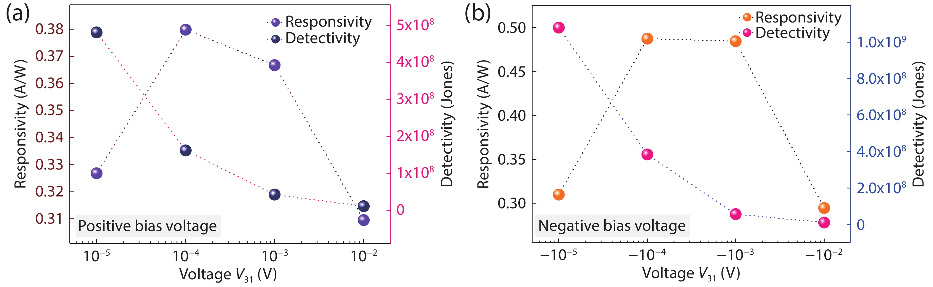
In this study, we present an in-depth exploration of charge transport phenomena and variable photo-switching characteristics in a novel double-perovskite-based three-terminal device. The Cs2AgBiBr6 thin film (TF) was synthesized through a three-step thermal evaporation process followed by precise open-air annealing, ensuring superior film quality as confirmed by structural and morphological characterizations. Photoluminescence spectroscopy revealed distinct emissions at 2.28 and 2.07 eV, indicative of both direct and indirect electronic transitions. Our device exhibited space-charge limited current (SCLC) behaviour beyond 0.35 V, aligning with the relationship $ {\text{Current}\left(I\right)\propto\text{Voltage\ }\left(V\right)^m }$, where the exponent m transitioned from ≤1 to >1. Detailed analysis of Schottky parameters within the trap-filled limit (TFL) regime was conducted, accounting for variations in temperature and optical power. Significantly, the self-powered photodetector demonstrated outstanding performance under illumination. The sensitivity of the device was finely tunable via the applied bias voltages at the third terminal. Notably, an optimal bias voltage of ±100 μV yielded maximum responsivity (R) of 0.48 A/W and an impressive detectivity (D*) of 1.07 × 10⁹ Jones, highlighting the potential of this double-perovskite-based device for advanced optoelectronic applications.