Issue Browser
Volume 45, Issue 6, Jun 2024
EDITORIAL
Preface to Special Topic on Integrated Circuits, Technologies and Applications
Zheng Wang, Xiaoyan Gui, Lin Cheng, Nanjian Wu
J. Semicond.  2024, 45(6): 060101  doi: 10.1088/1674-4926/24050901

SPECIAL TOPIC ARTICLES
A 16-bit 18-MSPS flash-assisted SAR ADC with hybrid synchronous and asynchronous control logic
Junyao Ji, Xinao Ji, Ziyu Zhou, Zhichao Dai, Xuhui Chen, Jie Zhang, Zheng Jiang, Hong Zhang
J. Semicond.  2024, 45(6): 062201  doi: 10.1088/1674-4926/23120049

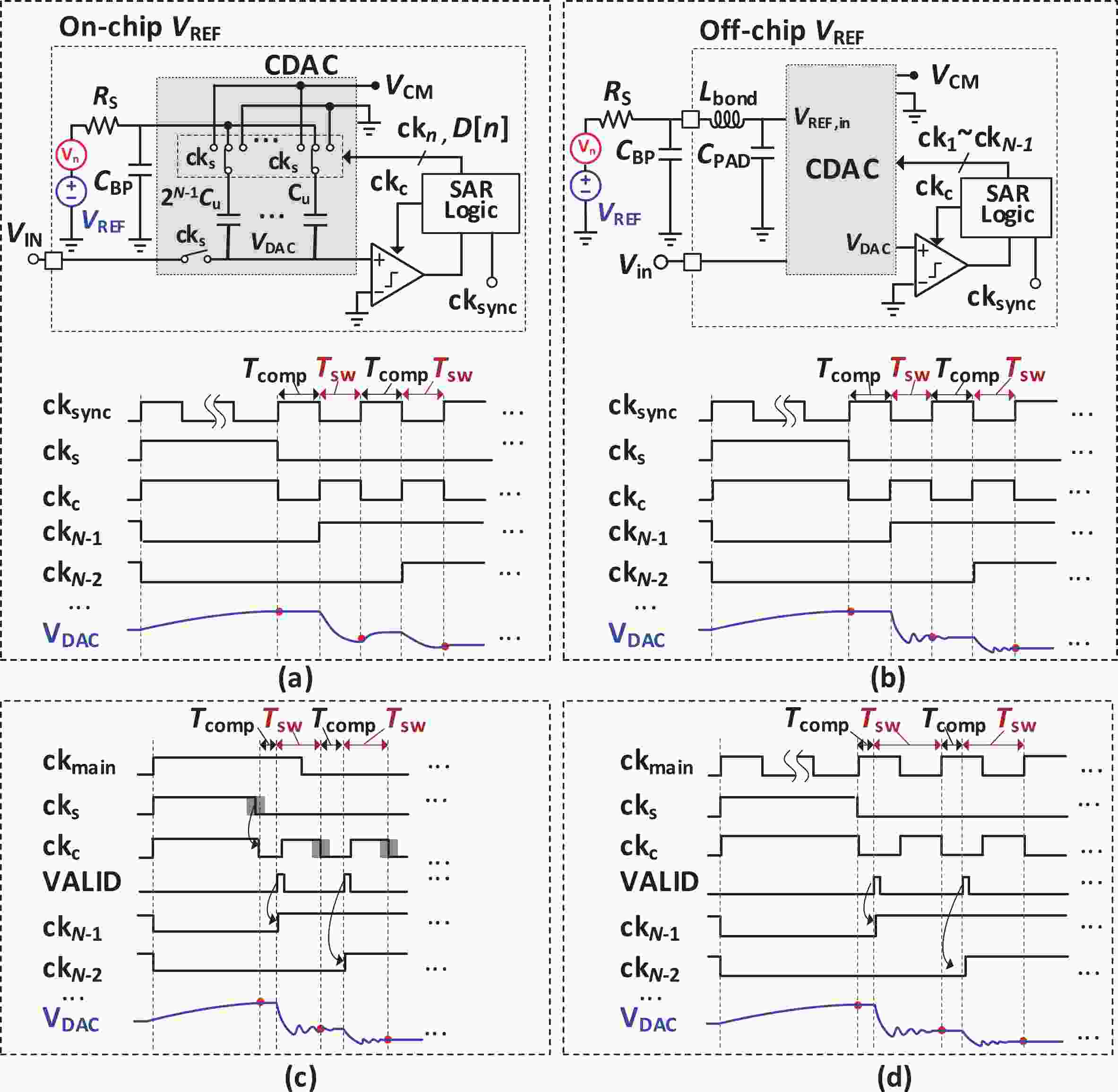
This paper presents a 16-bit, 18-MSPS (million samples per second) flash-assisted successive-approximation-register (SAR) analog-to-digital converter (ADC) utilizing hybrid synchronous and asynchronous (HYSAS) timing control logic based on an on-chip delay-locked loop (DLL). The HYSAS scheme can provide a longer settling time for the capacitive digital-to-analog converter (CDAC) than the synchronous and asynchronous SAR ADC. Therefore, the issue of incomplete settling or ringing in the DAC voltage for cases of either on-chip or off-chip reference voltage can be solved to a large extent. In addition, the foreground calibration of the CDAC’s mismatch is performed with a finite-impulse-response bandpass filter (FIR-BPF) based least-mean-square (LMS) algorithm in an off-chip FPGA (field programmable gate array). Fabricated in 40-nm CMOS process, the prototype ADC achieves 94.02-dB spurious-free dynamic range (SFDR), and 75.98-dB signal-to-noise-and-distortion ratio (SNDR) for a 2.88-MHz input under 18-MSPS sampling rate.
This paper presents a 16-bit, 18-MSPS (million samples per second) flash-assisted successive-approximation-register (SAR) analog-to-digital converter (ADC) utilizing hybrid synchronous and asynchronous (HYSAS) timing control logic based on an on-chip delay-locked loop (DLL). The HYSAS scheme can provide a longer settling time for the capacitive digital-to-analog converter (CDAC) than the synchronous and asynchronous SAR ADC. Therefore, the issue of incomplete settling or ringing in the DAC voltage for cases of either on-chip or off-chip reference voltage can be solved to a large extent. In addition, the foreground calibration of the CDAC’s mismatch is performed with a finite-impulse-response bandpass filter (FIR-BPF) based least-mean-square (LMS) algorithm in an off-chip FPGA (field programmable gate array). Fabricated in 40-nm CMOS process, the prototype ADC achieves 94.02-dB spurious-free dynamic range (SFDR), and 75.98-dB signal-to-noise-and-distortion ratio (SNDR) for a 2.88-MHz input under 18-MSPS sampling rate.
A frequency servo SoC with output power stabilization loop technology for miniaturized atomic clocks
Hongyang Zhang, Xinlin Geng, Zonglin Ye, Kailei Wang, Qian Xie, Zheng Wang
J. Semicond.  2024, 45(6): 062202  doi: 10.1088/1674-4926/23120056

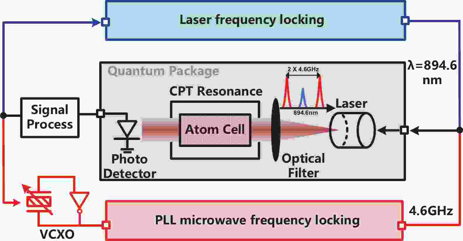
A frequency servo system-on-chip (FS-SoC) featuring output power stabilization technology is introduced in this study for high-precision and miniaturized cesium (Cs) atomic clocks. The proposed power stabilization loop (PSL) technique, incorporating an off-chip power detector (PD), ensures that the output power of the FS-SoC remains stable, mitigating the impact of power fluctuations on the atomic clock's stability. Additionally, a one-pulse-per-second (1PPS) is employed to synchronize the clock with GPS. Fabricated using 65 nm CMOS technology, the measured phase noise of the FS-SoC stands at −69.5 dBc/Hz@100 Hz offset and −83.9 dBc/Hz@1 kHz offset, accompanied by a power dissipation of 19.7 mW. The Cs atomic clock employing the proposed FS-SoC and PSL obtains an Allan deviation of 1.7 × 10⁻¹¹ with 1-s averaging time.
A frequency servo system-on-chip (FS-SoC) featuring output power stabilization technology is introduced in this study for high-precision and miniaturized cesium (Cs) atomic clocks. The proposed power stabilization loop (PSL) technique, incorporating an off-chip power detector (PD), ensures that the output power of the FS-SoC remains stable, mitigating the impact of power fluctuations on the atomic clock's stability. Additionally, a one-pulse-per-second (1PPS) is employed to synchronize the clock with GPS. Fabricated using 65 nm CMOS technology, the measured phase noise of the FS-SoC stands at −69.5 dBc/Hz@100 Hz offset and −83.9 dBc/Hz@1 kHz offset, accompanied by a power dissipation of 19.7 mW. The Cs atomic clock employing the proposed FS-SoC and PSL obtains an Allan deviation of 1.7 × 10⁻¹¹ with 1-s averaging time.
An NMOS output-capacitorless low-dropout regulator with dynamic-strength event-driven charge pump
Yiling Xie, Baochuang Wang, Dihu Chen, Jianping Guo
J. Semicond.  2024, 45(6): 062203  doi: 10.1088/1674-4926/23120057

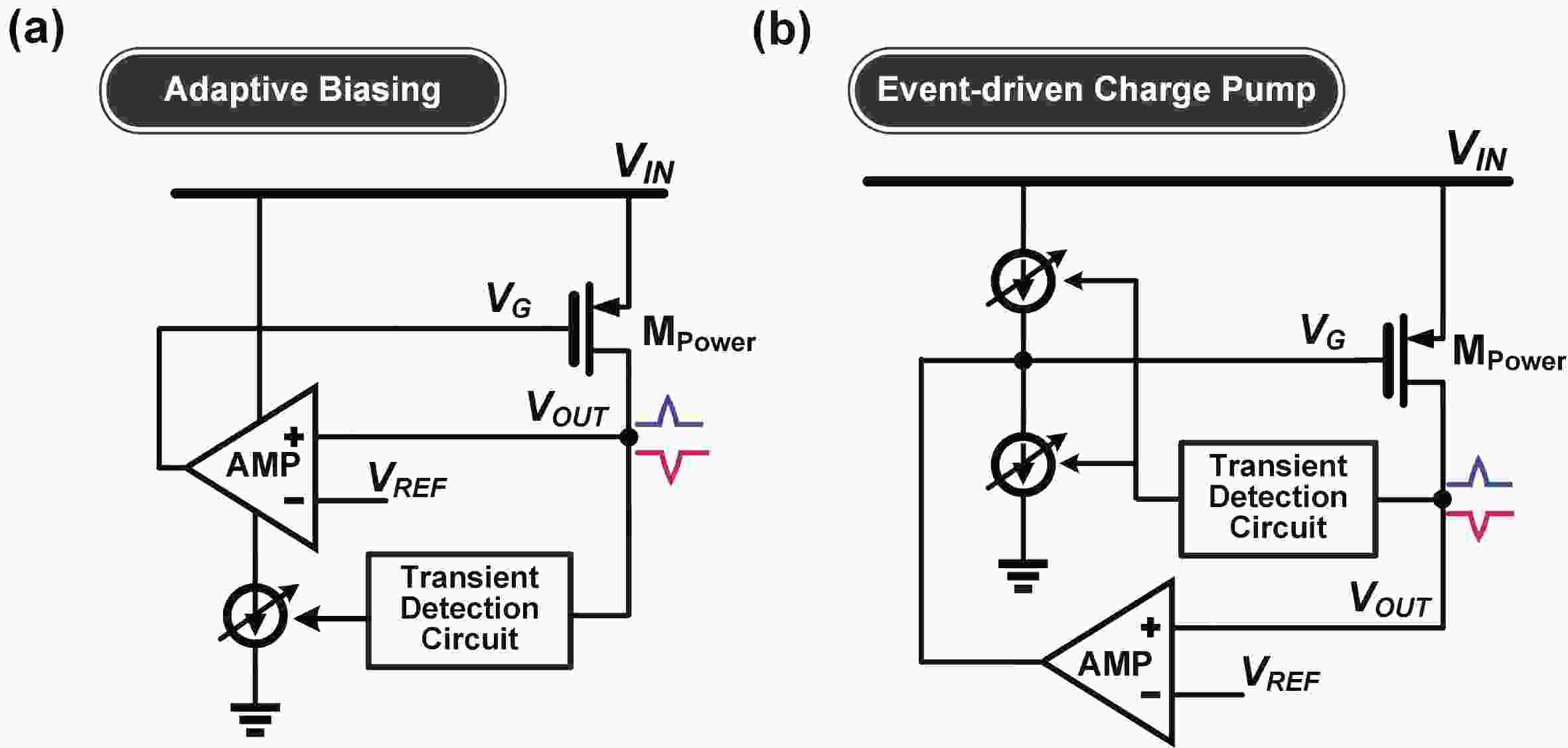
In this paper, an NMOS output-capacitorless low-dropout regulator (OCL-LDO) featuring dual-loop regulation has been proposed, achieving fast transient response with low power consumption. An event-driven charge pump (CP) loop with the dynamic strength control (DSC), is proposed in this paper, which overcomes trade-offs inherent in conventional structures. The presented design addresses and resolves the large signal stability issue, which has been previously overlooked in the event-driven charge pump structure. This breakthrough allows for the full exploitation of the charge-pump structure's potential, particularly in enhancing transient recovery. Moreover, a dynamic error amplifier is utilized to attain precise regulation of the steady-state output voltage, leading to favorable static characteristics. A prototype chip has been fabricated in 65 nm CMOS technology. The measurement results show that the proposed OCL-LDO achieves a 410 nA low quiescent current (IQ) and can recover within 30 ns under 200 mA/10 ns loading change.
In this paper, an NMOS output-capacitorless low-dropout regulator (OCL-LDO) featuring dual-loop regulation has been proposed, achieving fast transient response with low power consumption. An event-driven charge pump (CP) loop with the dynamic strength control (DSC), is proposed in this paper, which overcomes trade-offs inherent in conventional structures. The presented design addresses and resolves the large signal stability issue, which has been previously overlooked in the event-driven charge pump structure. This breakthrough allows for the full exploitation of the charge-pump structure's potential, particularly in enhancing transient recovery. Moreover, a dynamic error amplifier is utilized to attain precise regulation of the steady-state output voltage, leading to favorable static characteristics. A prototype chip has been fabricated in 65 nm CMOS technology. The measurement results show that the proposed OCL-LDO achieves a 410 nA low quiescent current (IQ) and can recover within 30 ns under 200 mA/10 ns loading change.
A 28/56 Gb/s NRZ/PAM-4 dual-mode transceiver with 1/4 rate reconfigurable 4-tap FFE and half-rate slicer in a 28-nm CMOS
Yukun He, Zhao Yuan, Kanan Wang, Renjie Tang, Yunxiang He, Xian Chen, Zhengyang Ye, Xiaoyan Gui
J. Semicond.  2024, 45(6): 062204  doi: 10.1088/1674-4926/24010001

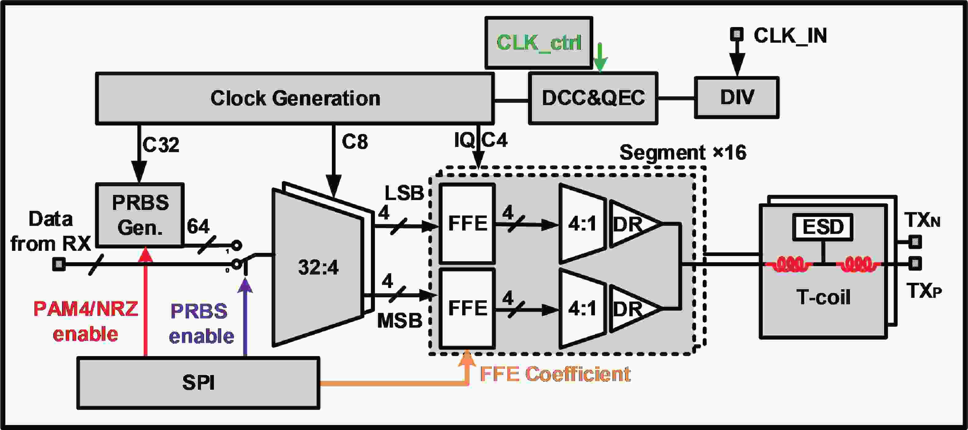
A 28/56 Gb/s NRZ/PAM-4 dual-mode transceiver (TRx) designed in a 28-nm complementary metal-oxide-semiconductor (CMOS) process is presented in this article. A voltage-mode (VM) driver featuring a 4-tap reconfigurable feed-forward equalizer (FFE) is employed in the quarter-rate transmitter (TX). The half-rate receiver (RX) incorporates a continuous-time linear equalizer (CTLE), a 3-stage high-speed slicer with multi-clock-phase sampling, and a clock and data recovery (CDR). The experimental results show that the TRx operates at a maximum speed of 56 Gb/s with chip-on board (COB) assembly. The 28 Gb/s NRZ eye diagram shows a far-end vertical eye opening of 210 mV with an output amplitude of 351 mV single-ended and the 56 Gb/s PAM-4 eye diagram exhibits far-end eye opening of 33 mV (upper-eye), 31 mV (mid-eye), and 28 mV (lower-eye) with an output amplitude of 353 mV single-ended. The recovered 14 GHz clock from the RX exhibits random jitter (RJ) of 469 fs and deterministic jitter (DJ) of 8.76 ps. The 875 Mb/s de-multiplexed data features 593 ps horizontal eye opening with 32.02 ps RJ, at bit-error rate (BER) of 10−5 (0.53 UI). The power dissipation of TX and RX are 125 and 181.4 mW, respectively, from a 0.9-V supply.
A 28/56 Gb/s NRZ/PAM-4 dual-mode transceiver (TRx) designed in a 28-nm complementary metal-oxide-semiconductor (CMOS) process is presented in this article. A voltage-mode (VM) driver featuring a 4-tap reconfigurable feed-forward equalizer (FFE) is employed in the quarter-rate transmitter (TX). The half-rate receiver (RX) incorporates a continuous-time linear equalizer (CTLE), a 3-stage high-speed slicer with multi-clock-phase sampling, and a clock and data recovery (CDR). The experimental results show that the TRx operates at a maximum speed of 56 Gb/s with chip-on board (COB) assembly. The 28 Gb/s NRZ eye diagram shows a far-end vertical eye opening of 210 mV with an output amplitude of 351 mV single-ended and the 56 Gb/s PAM-4 eye diagram exhibits far-end eye opening of 33 mV (upper-eye), 31 mV (mid-eye), and 28 mV (lower-eye) with an output amplitude of 353 mV single-ended. The recovered 14 GHz clock from the RX exhibits random jitter (RJ) of 469 fs and deterministic jitter (DJ) of 8.76 ps. The 875 Mb/s de-multiplexed data features 593 ps horizontal eye opening with 32.02 ps RJ, at bit-error rate (BER) of 10−5 (0.53 UI). The power dissipation of TX and RX are 125 and 181.4 mW, respectively, from a 0.9-V supply.
REVIEWS
Neuromorphic circuits based on memristors: endowing robots with a human-like brain
Xuemei Wang, Fan Yang, Qing Liu, Zien Zhang, Zhixing Wen, Jiangang Chen, Qirui Zhang, Cheng Wang, Ge Wang, Fucai Liu
J. Semicond.  2024, 45(6): 061301  doi: 10.1088/1674-4926/23120037

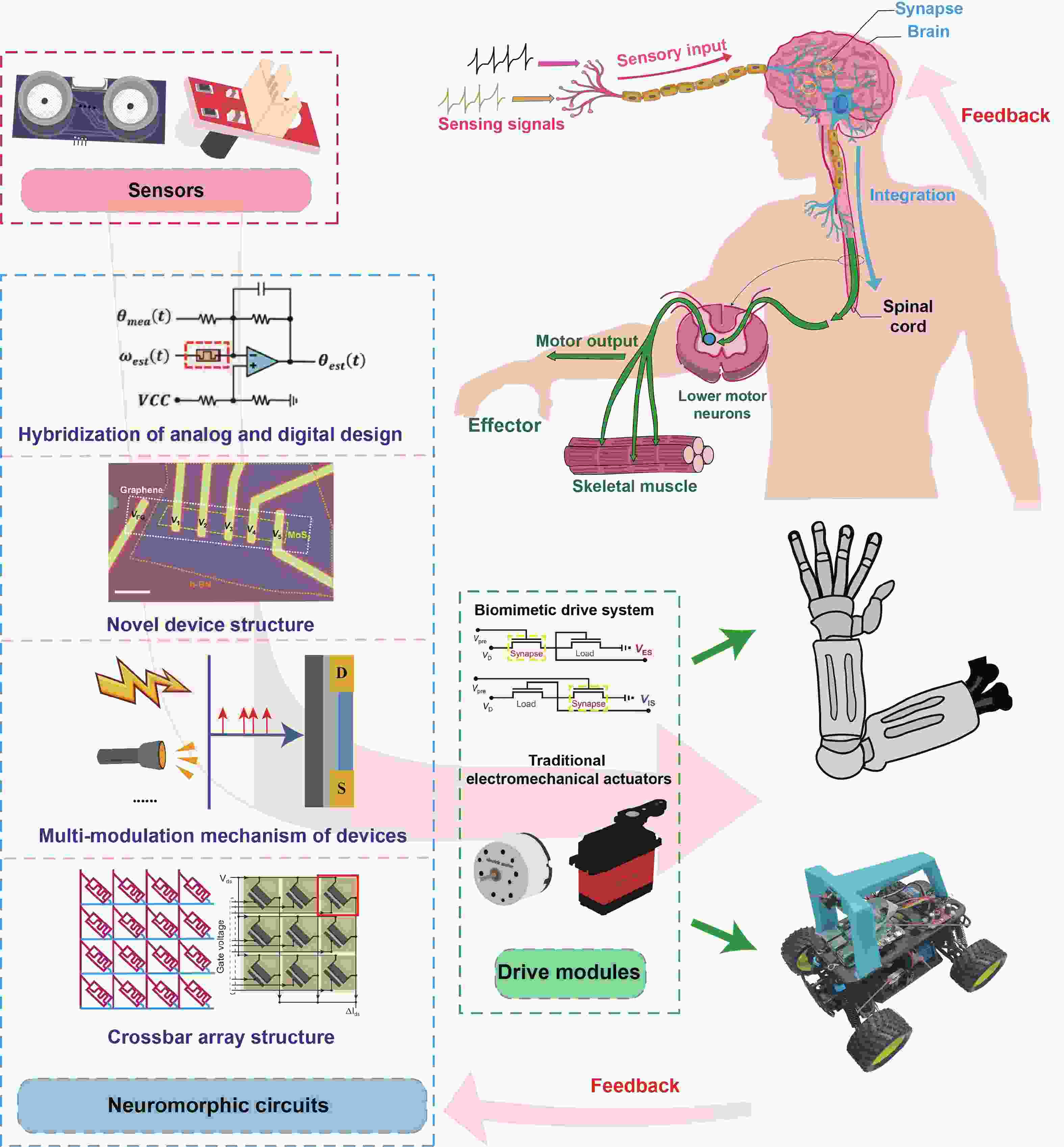
Robots are widely used, providing significant convenience in daily life and production. With the rapid development of artificial intelligence and neuromorphic computing in recent years, the realization of more intelligent robots through a profound intersection of neuroscience and robotics has received much attention. Neuromorphic circuits based on memristors used to construct hardware neural networks have proved to be a promising solution of shattering traditional control limitations in the field of robot control, showcasing characteristics that enhance robot intelligence, speed, and energy efficiency. Starting with introducing the working mechanism of memristors and peripheral circuit design, this review gives a comprehensive analysis on the biomimetic information processing and biomimetic driving operations achieved through the utilization of neuromorphic circuits in brain-like control. Four hardware neural network approaches, including digital-analog hybrid circuit design, novel device structure design, multi-regulation mechanism, and crossbar array, are summarized, which can well simulate the motor decision-making mechanism, multi-information integration and parallel control of brain at the hardware level. It will be definitely conductive to promote the application of memristor-based neuromorphic circuits in areas such as intelligent robotics, artificial intelligence, and neural computing. Finally, a conclusion and future prospects are discussed.
Robots are widely used, providing significant convenience in daily life and production. With the rapid development of artificial intelligence and neuromorphic computing in recent years, the realization of more intelligent robots through a profound intersection of neuroscience and robotics has received much attention. Neuromorphic circuits based on memristors used to construct hardware neural networks have proved to be a promising solution of shattering traditional control limitations in the field of robot control, showcasing characteristics that enhance robot intelligence, speed, and energy efficiency. Starting with introducing the working mechanism of memristors and peripheral circuit design, this review gives a comprehensive analysis on the biomimetic information processing and biomimetic driving operations achieved through the utilization of neuromorphic circuits in brain-like control. Four hardware neural network approaches, including digital-analog hybrid circuit design, novel device structure design, multi-regulation mechanism, and crossbar array, are summarized, which can well simulate the motor decision-making mechanism, multi-information integration and parallel control of brain at the hardware level. It will be definitely conductive to promote the application of memristor-based neuromorphic circuits in areas such as intelligent robotics, artificial intelligence, and neural computing. Finally, a conclusion and future prospects are discussed.
Complementary memtransistors for neuromorphic computing: How, what and why
Qi Chen, Yue Zhou, Weiwei Xiong, Zirui Chen, Yasai Wang, Xiangshui Miao, Yuhui He
J. Semicond.  2024, 45(6): 061701  doi: 10.1088/1674-4926/23120051

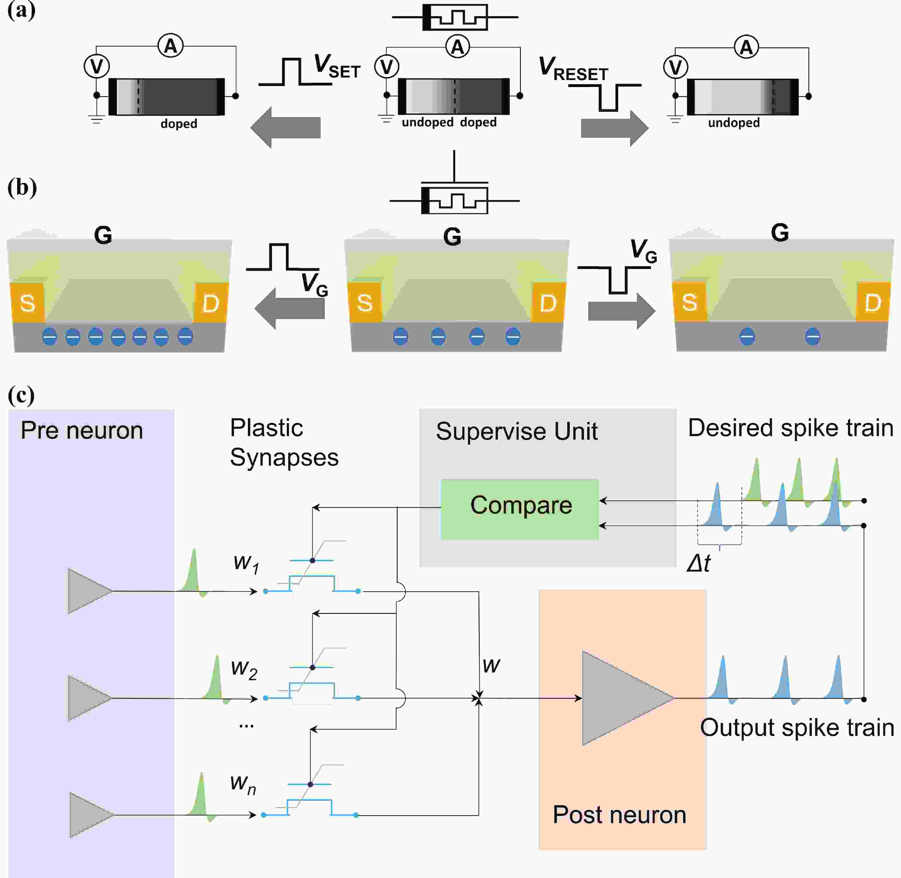
Memtransistors in which the source−drain channel conductance can be nonvolatilely manipulated through the gate signals have emerged as promising components for implementing neuromorphic computing. On the other side, it is known that the complementary metal-oxide-semiconductor (CMOS) field effect transistors have played the fundamental role in the modern integrated circuit technology. Therefore, will complementary memtransistors (CMT) also play such a role in the future neuromorphic circuits and chips? In this review, various types of materials and physical mechanisms for constructing CMT (how) are inspected with their merits and need-to-address challenges discussed. Then the unique properties (what) and potential applications of CMT in different learning algorithms/scenarios of spiking neural networks (why) are reviewed, including supervised rule, reinforcement one, dynamic vision with in-sensor computing, etc. Through exploiting the complementary structure-related novel functions, significant reduction of hardware consuming, enhancement of energy/efficiency ratio and other advantages have been gained, illustrating the alluring prospect of design technology co-optimization (DTCO) of CMT towards neuromorphic computing.
Memtransistors in which the source−drain channel conductance can be nonvolatilely manipulated through the gate signals have emerged as promising components for implementing neuromorphic computing. On the other side, it is known that the complementary metal-oxide-semiconductor (CMOS) field effect transistors have played the fundamental role in the modern integrated circuit technology. Therefore, will complementary memtransistors (CMT) also play such a role in the future neuromorphic circuits and chips? In this review, various types of materials and physical mechanisms for constructing CMT (how) are inspected with their merits and need-to-address challenges discussed. Then the unique properties (what) and potential applications of CMT in different learning algorithms/scenarios of spiking neural networks (why) are reviewed, including supervised rule, reinforcement one, dynamic vision with in-sensor computing, etc. Through exploiting the complementary structure-related novel functions, significant reduction of hardware consuming, enhancement of energy/efficiency ratio and other advantages have been gained, illustrating the alluring prospect of design technology co-optimization (DTCO) of CMT towards neuromorphic computing.
ARTICLES
Recess-free enhancement-mode AlGaN/GaN RF HEMTs on Si substrate
Tiantian Luan, Sen Huang, Guanjun Jing, Jie Fan, Haibo Yin, Xinguo Gao, Sheng Zhang, Ke Wei, Yankui Li, Qimeng Jiang, Xinhua Wang, Bin Hou, Ling Yang, Xiaohua Ma, Xinyu Liu
J. Semicond.  2024, 45(6): 062301  doi: 10.1088/1674-4926/23120006

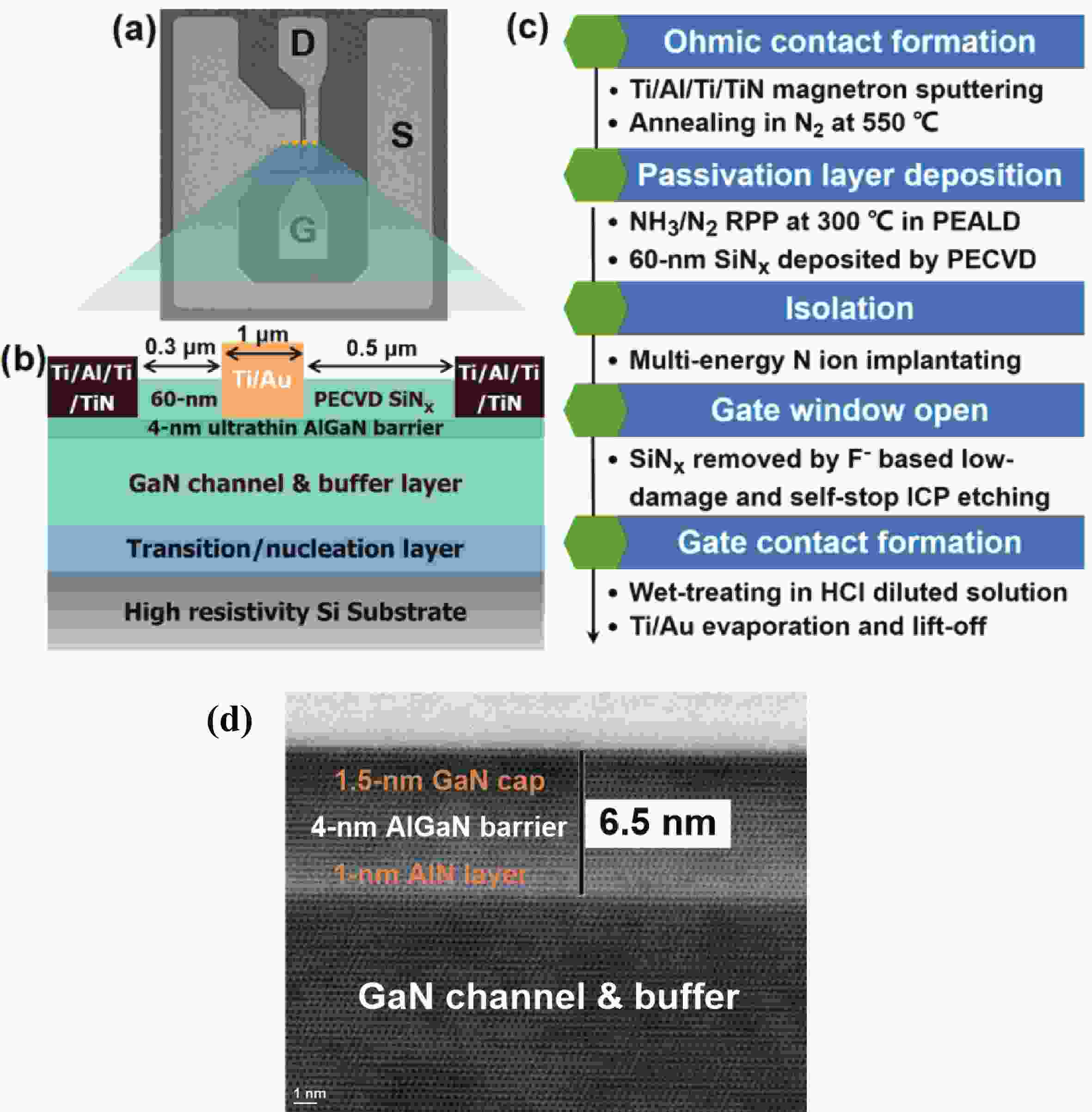
Enhancement-mode (E-mode) GaN-on-Si radio-frequency (RF) high-electron-mobility transistors (HEMTs) were fabricated on an ultrathin-barrier (UTB) AlGaN (<6 nm)/GaN heterostructure featuring a naturally depleted 2-D electron gas (2DEG) channel. The fabricated E-mode HEMTs exhibit a relatively high threshold voltage (VTH) of +1.1 V with good uniformity. A maximum current/power gain cut-off frequency (fT/fMAX) of 31.3/99.6 GHz with a power added efficiency (PAE) of 52.47% and an output power density (Pout) of 1.0 W/mm at 3.5 GHz were achieved on the fabricated E-mode HEMTs with 1-µm gate and Au-free ohmic contact.
Enhancement-mode (E-mode) GaN-on-Si radio-frequency (RF) high-electron-mobility transistors (HEMTs) were fabricated on an ultrathin-barrier (UTB) AlGaN (<6 nm)/GaN heterostructure featuring a naturally depleted 2-D electron gas (2DEG) channel. The fabricated E-mode HEMTs exhibit a relatively high threshold voltage (VTH) of +1.1 V with good uniformity. A maximum current/power gain cut-off frequency (fT/fMAX) of 31.3/99.6 GHz with a power added efficiency (PAE) of 52.47% and an output power density (Pout) of 1.0 W/mm at 3.5 GHz were achieved on the fabricated E-mode HEMTs with 1-µm gate and Au-free ohmic contact.
Phase-locked single-mode terahertz quantum cascade lasers array
Yunfei Xu, Weijiang Li, Yu Ma, Quanyong Lu, Jinchuan Zhang, Shenqiang Zhai, Ning Zhuo, Junqi Liu, Shuman Liu, Fengmin Cheng, Lijun Wang, Fengqi Liu
J. Semicond.  2024, 45(6): 062401  doi: 10.1088/1674-4926/23120010

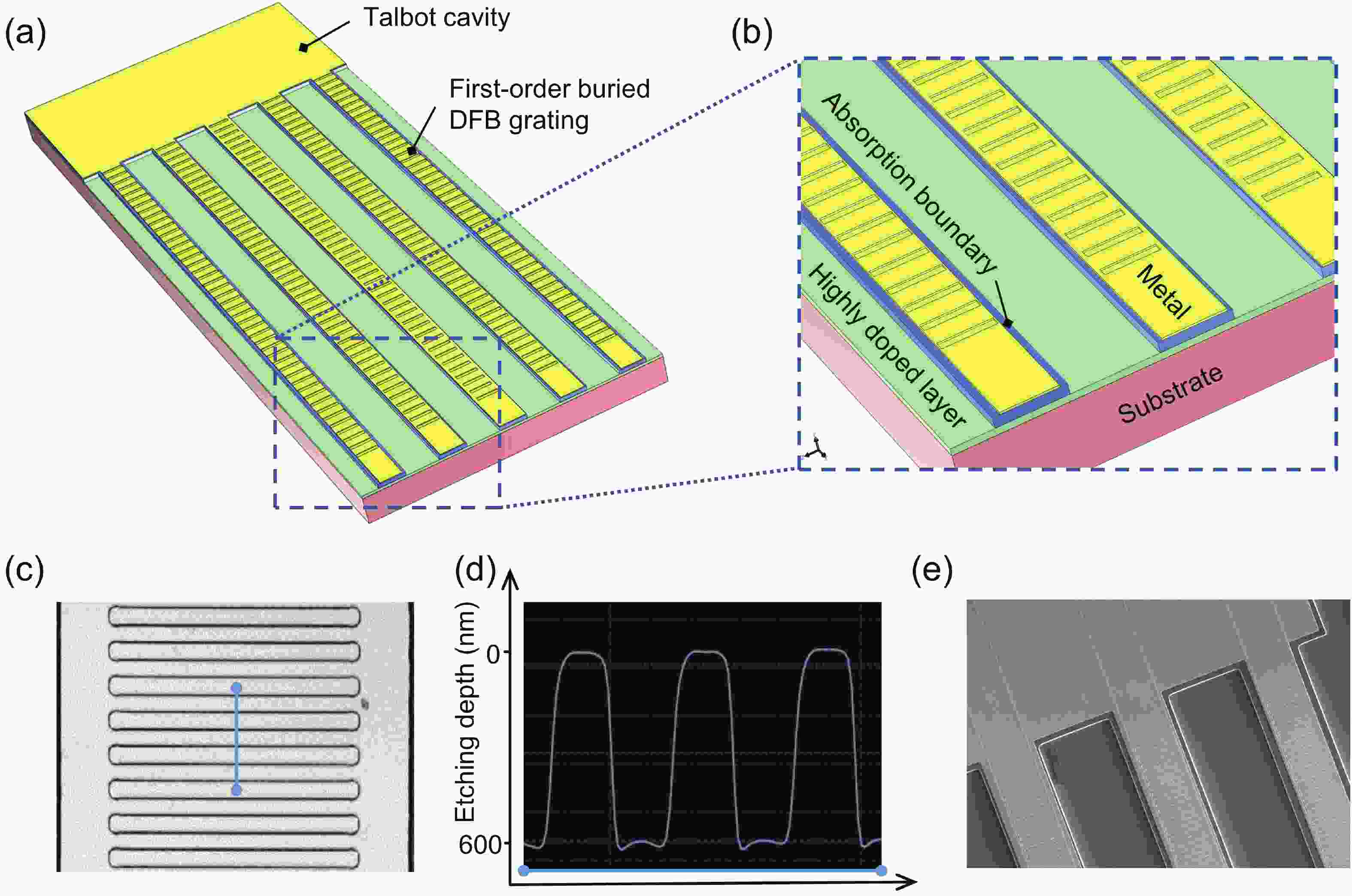
We demonstrated a scheme of phase-locked terahertz quantum cascade lasers (THz QCLs) array, with a single-mode pulse power of 108 mW at 13 K. The device utilizes a Talbot cavity to achieve phase locking among five ridge lasers with first-order buried distributed feedback (DFB) grating, resulting in nearly five times amplification of the single-mode power. Due to the optimum length of Talbot cavity depends on wavelength, the combination of Talbot cavity with the DFB grating leads to better power amplification than the combination with multimode Fabry−Perot (F−P) cavities. The Talbot cavity facet reflects light back to the ridge array direction and achieves self-imaging in the array, enabling phase-locked operation of ridges. We set the spacing between adjacent elements to be 220 μm, much larger than the free-space wavelength, ensuring the operation of the fundamental supermode throughout the laser's dynamic range and obtaining a high-brightness far-field distribution. This scheme provides a new approach for enhancing the single-mode power of THz QCLs.

We demonstrated a scheme of phase-locked terahertz quantum cascade lasers (THz QCLs) array, with a single-mode pulse power of 108 mW at 13 K. The device utilizes a Talbot cavity to achieve phase locking among five ridge lasers with first-order buried distributed feedback (DFB) grating, resulting in nearly five times amplification of the single-mode power. Due to the optimum length of Talbot cavity depends on wavelength, the combination of Talbot cavity with the DFB grating leads to better power amplification than the combination with multimode Fabry−Perot (F−P) cavities. The Talbot cavity facet reflects light back to the ridge array direction and achieves self-imaging in the array, enabling phase-locked operation of ridges. We set the spacing between adjacent elements to be 220 μm, much larger than the free-space wavelength, ensuring the operation of the fundamental supermode throughout the laser's dynamic range and obtaining a high-brightness far-field distribution. This scheme provides a new approach for enhancing the single-mode power of THz QCLs.
Control of GaN inverted pyramids growth on c-plane patterned sapphire substrates
Luming Yu, Xun Wang, Zhibiao Hao, Yi Luo, Changzheng Sun, Bing Xiong, Yanjun Han, Jian Wang, Hongtao Li, Lin Gan, Lai Wang
J. Semicond.  2024, 45(6): 062501  doi: 10.1088/1674-4926/24010013

Growth of gallium nitride (GaN) inverted pyramids on c-plane sapphire substrates is benefit for fabricating novel devices as it forms the semipolar facets. In this work, GaN inverted pyramids are directly grown on c-plane patterned sapphire substrates (PSS) by metal organic vapor phase epitaxy (MOVPE). The influences of growth conditions on the surface morphology are experimentally studied and explained by Wulff constructions. The competition of growth rate among {0001}, {$ 10\bar{\text{1}}1 $}, and {$11 \bar{\text{2}}2 $} facets results in the various surface morphologies of GaN. A higher growth temperature of 985 °C and a lower Ⅴ/Ⅲ ratio of 25 can expand the area of {$ 11\bar{\text{2}}2 $} facets in GaN inverted pyramids. On the other hand, GaN inverted pyramids with almost pure {$10 \bar{\text{1}}1 $} facets are obtained by using a lower growth temperature of 930 °C, a higher Ⅴ/Ⅲ ratio of 100, and PSS with pattern arrangement perpendicular to the substrate primary flat.

Growth of gallium nitride (GaN) inverted pyramids on c-plane sapphire substrates is benefit for fabricating novel devices as it forms the semipolar facets. In this work, GaN inverted pyramids are directly grown on c-plane patterned sapphire substrates (PSS) by metal organic vapor phase epitaxy (MOVPE). The influences of growth conditions on the surface morphology are experimentally studied and explained by Wulff constructions. The competition of growth rate among {0001}, {$ 10\bar{\text{1}}1 $}, and {$11 \bar{\text{2}}2 $} facets results in the various surface morphologies of GaN. A higher growth temperature of 985 °C and a lower Ⅴ/Ⅲ ratio of 25 can expand the area of {$ 11\bar{\text{2}}2 $} facets in GaN inverted pyramids. On the other hand, GaN inverted pyramids with almost pure {$10 \bar{\text{1}}1 $} facets are obtained by using a lower growth temperature of 930 °C, a higher Ⅴ/Ⅲ ratio of 100, and PSS with pattern arrangement perpendicular to the substrate primary flat.