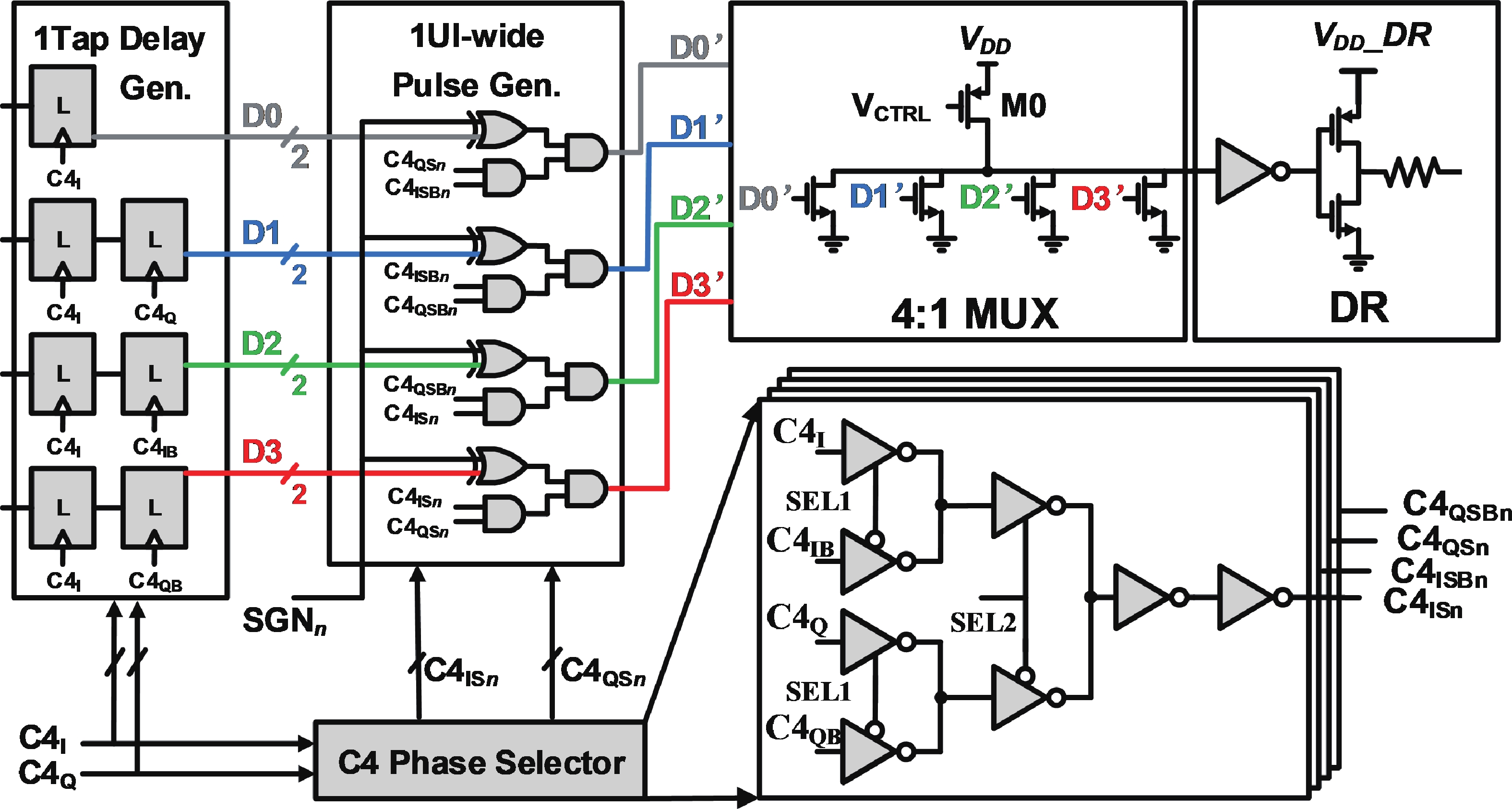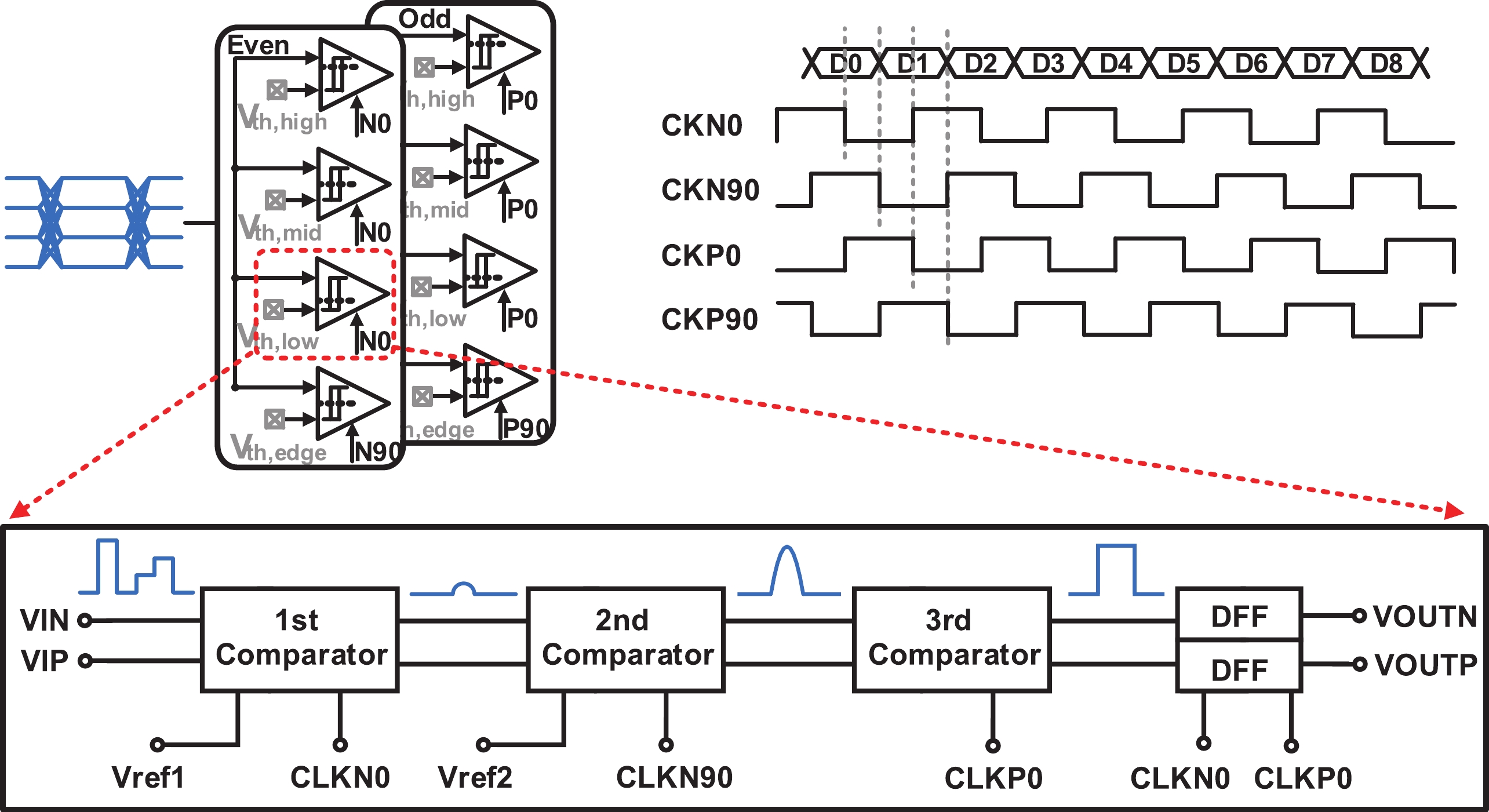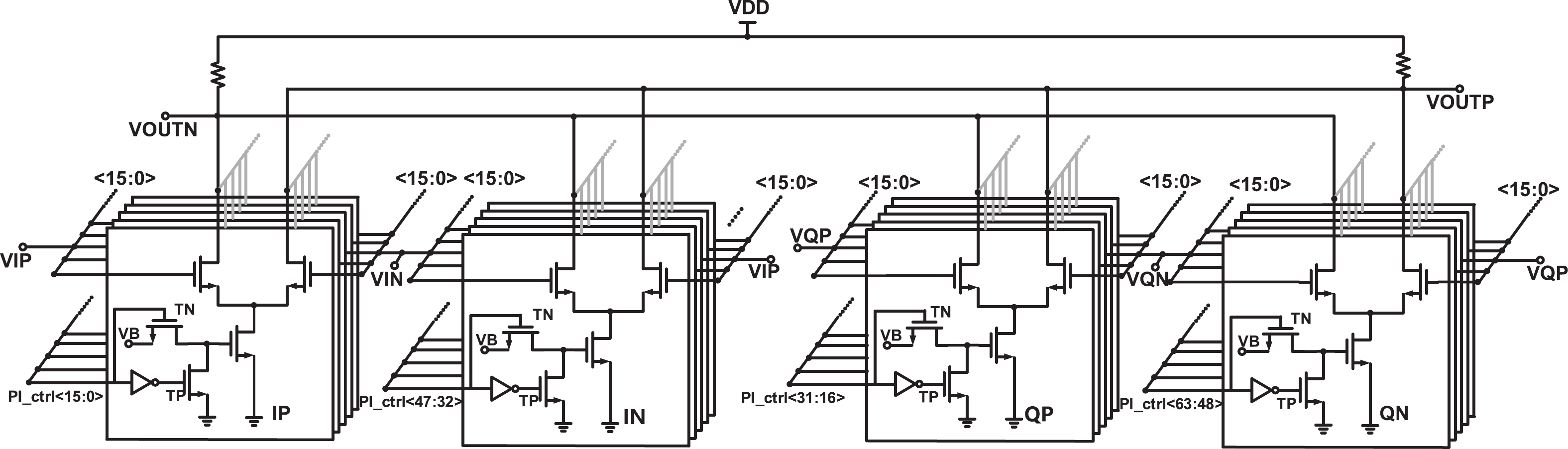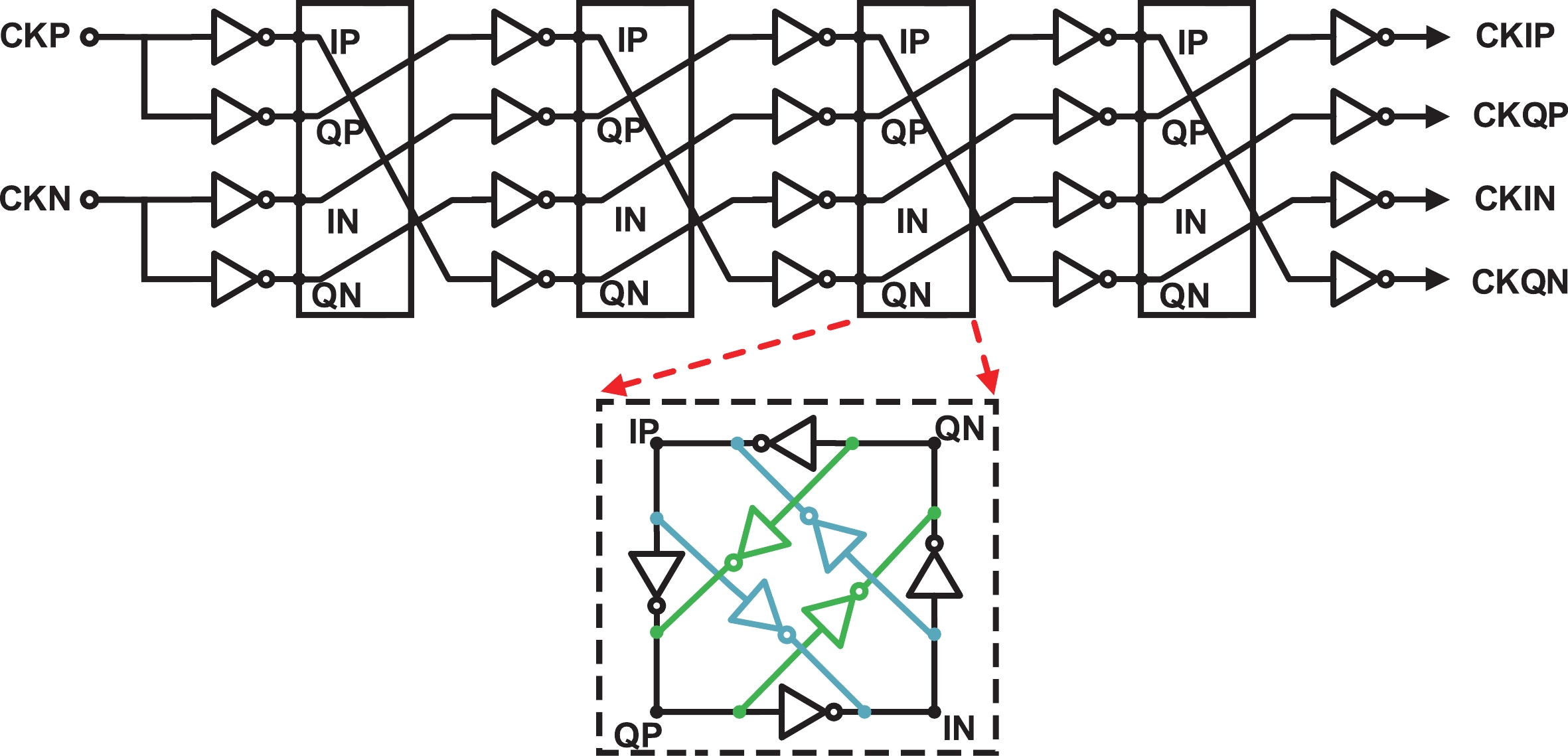
Fig. 1.
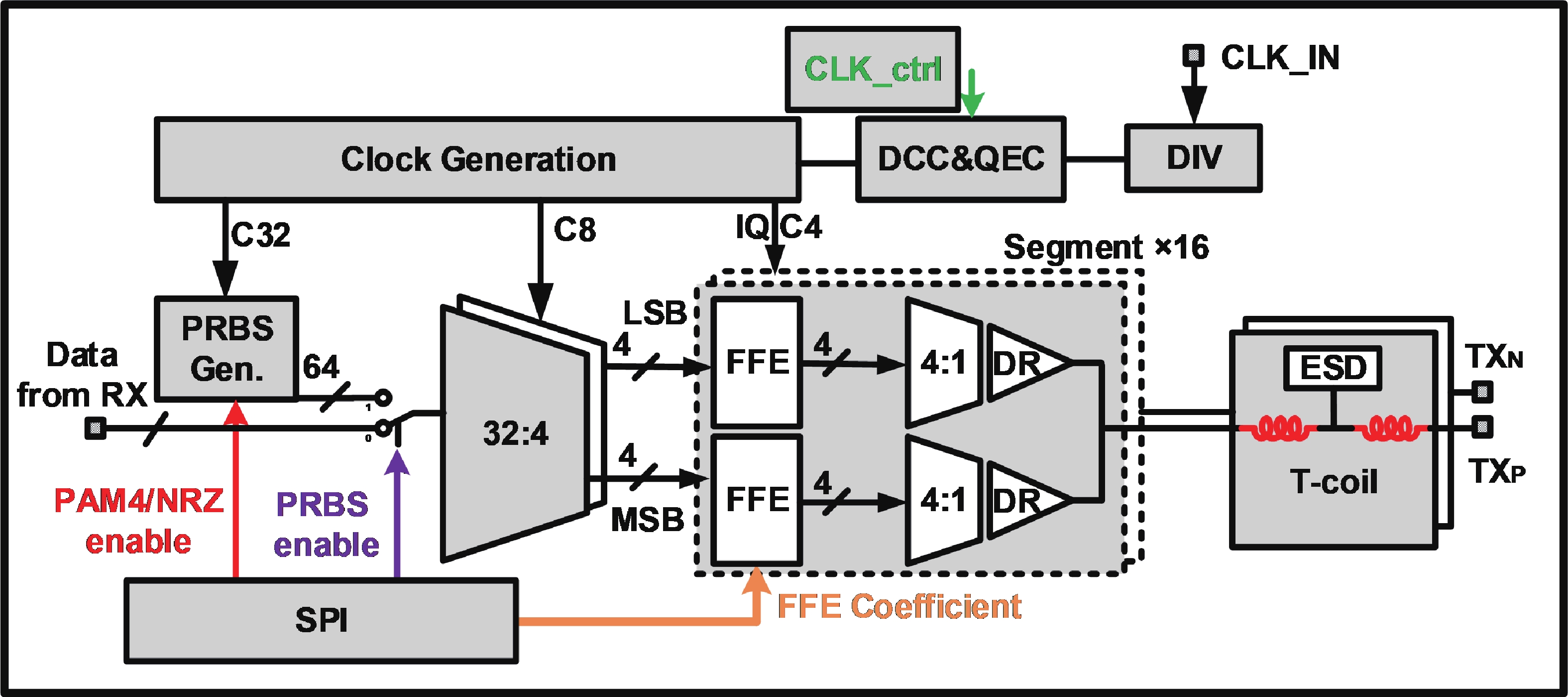
(Color online) TX architecture.
SPECIAL TOPIC ARTICLES
Yukun He, Zhao Yuan, Kanan Wang, Renjie Tang, Yunxiang He, Xian Chen, Zhengyang Ye and Xiaoyan Gui
Corresponding author: Xiaoyan Gui, xy.gui@xjtu.edu.cn
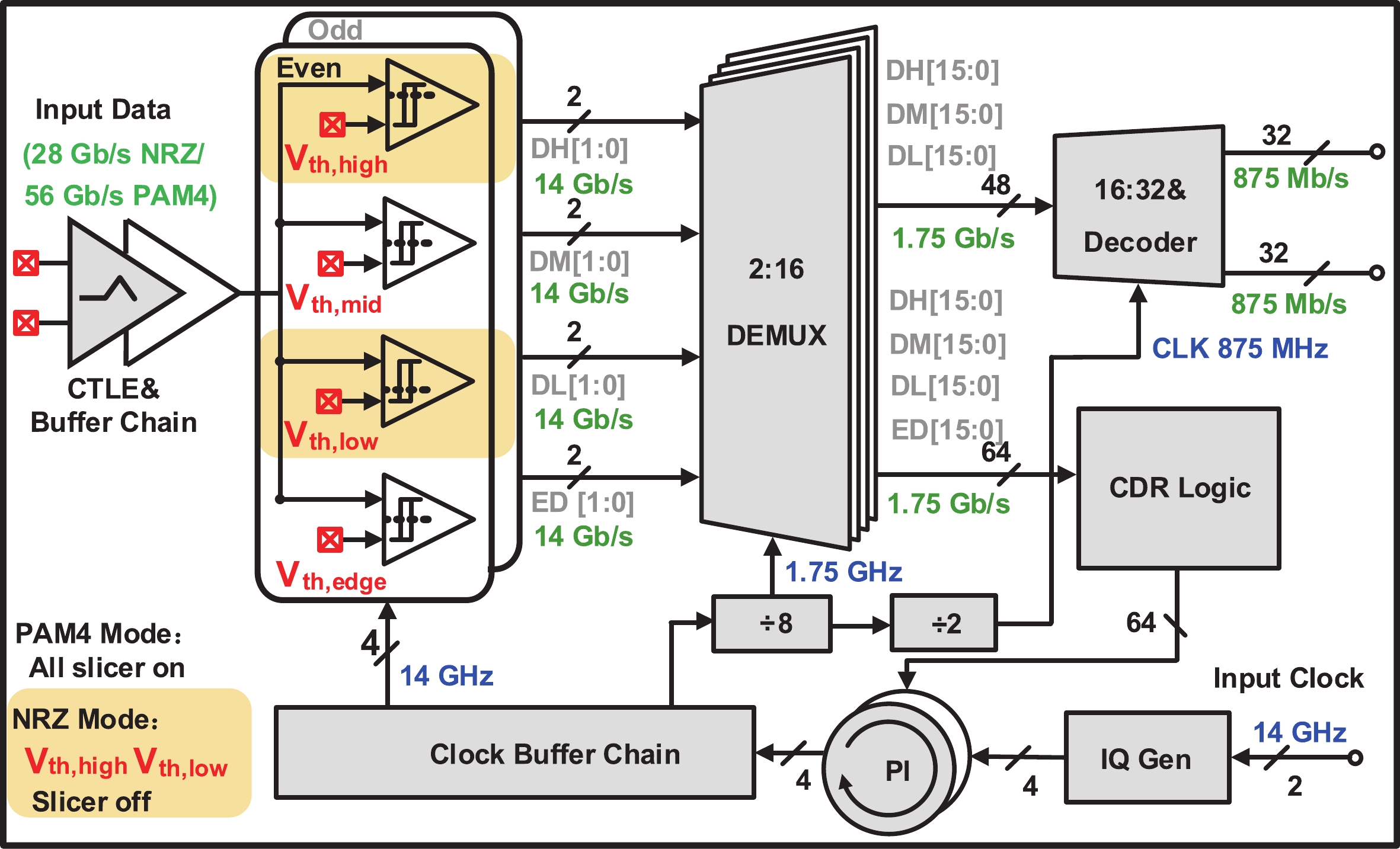
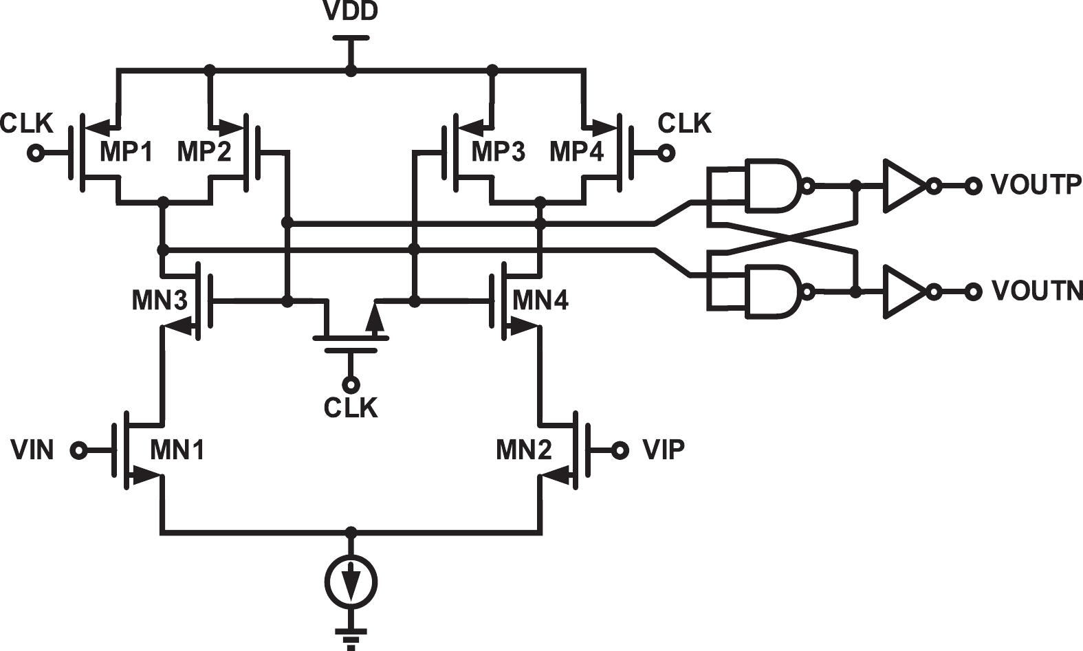
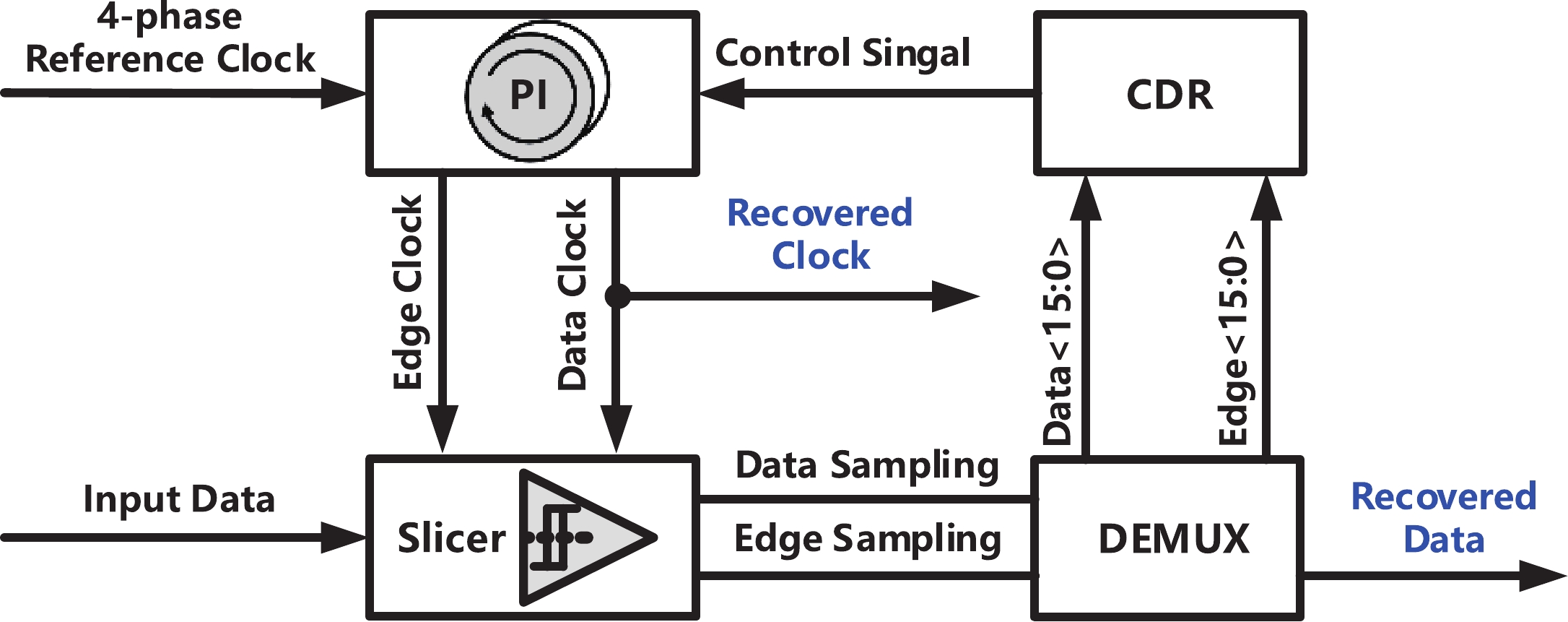
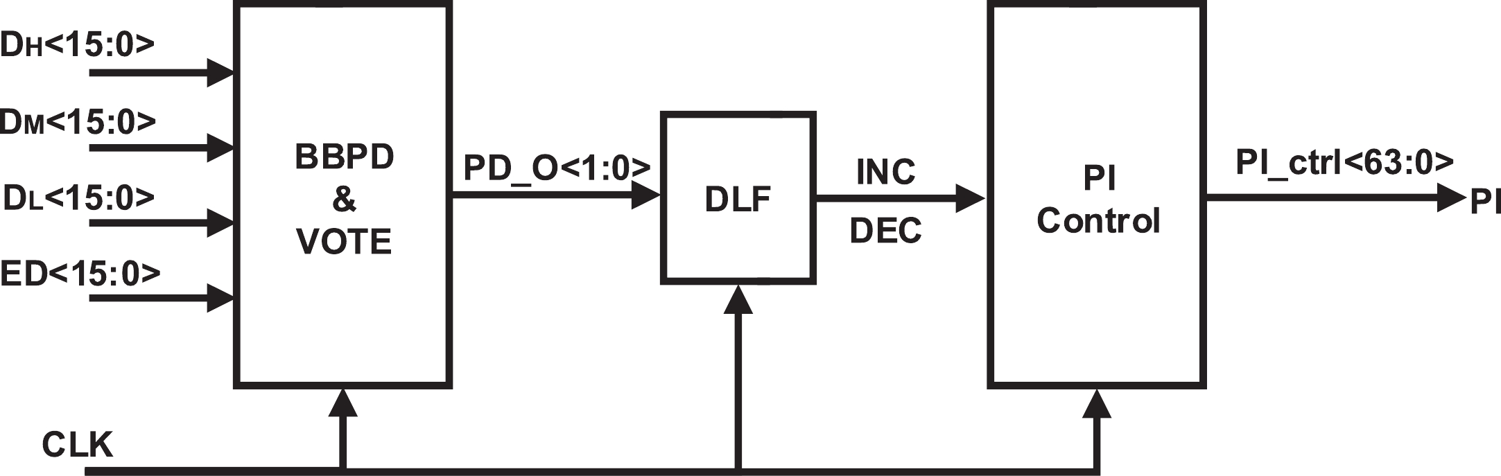
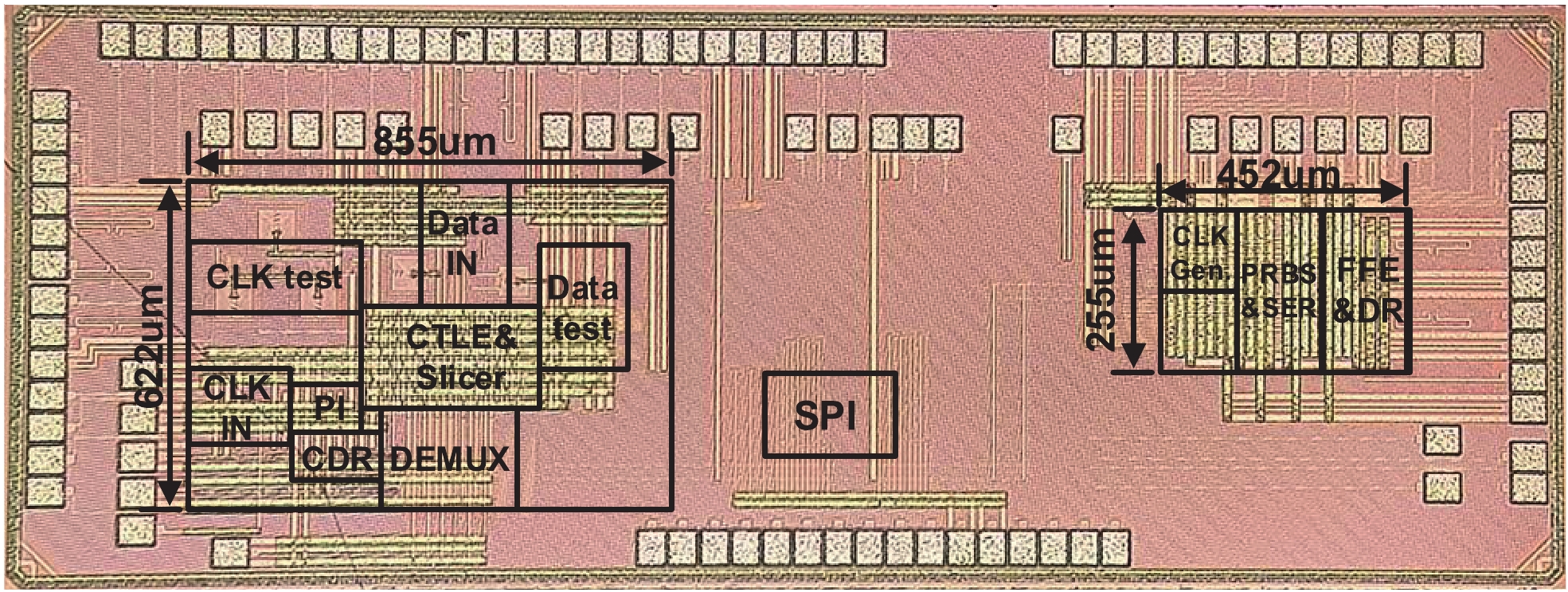
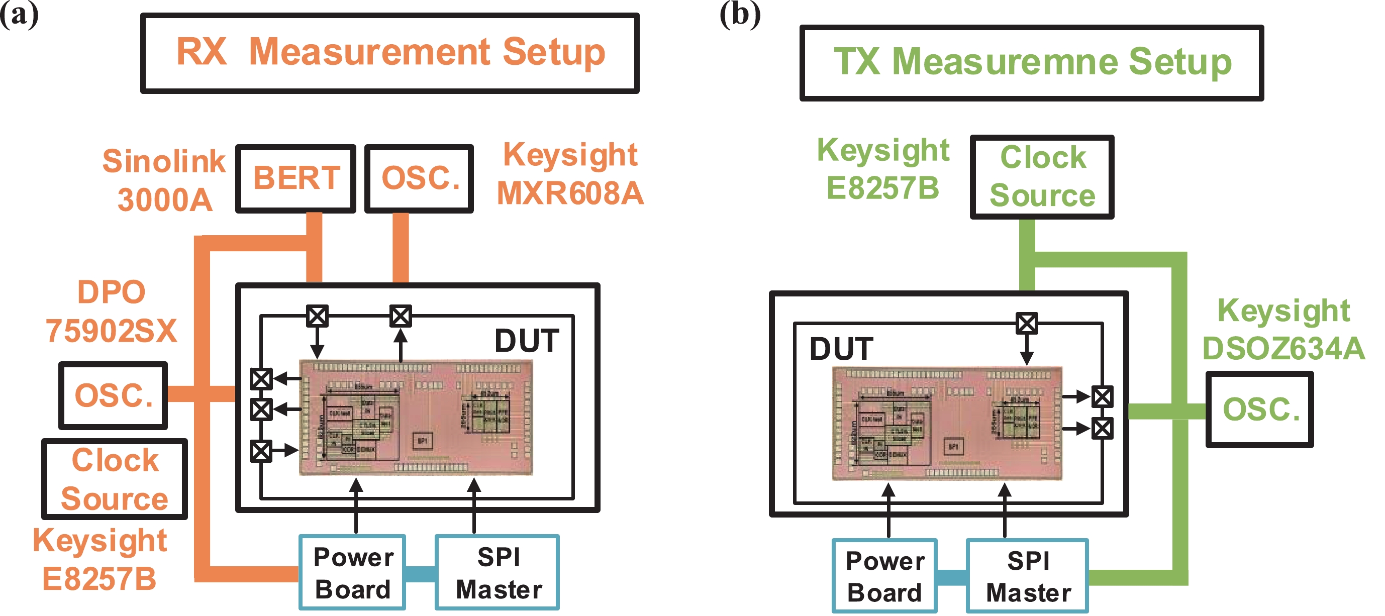
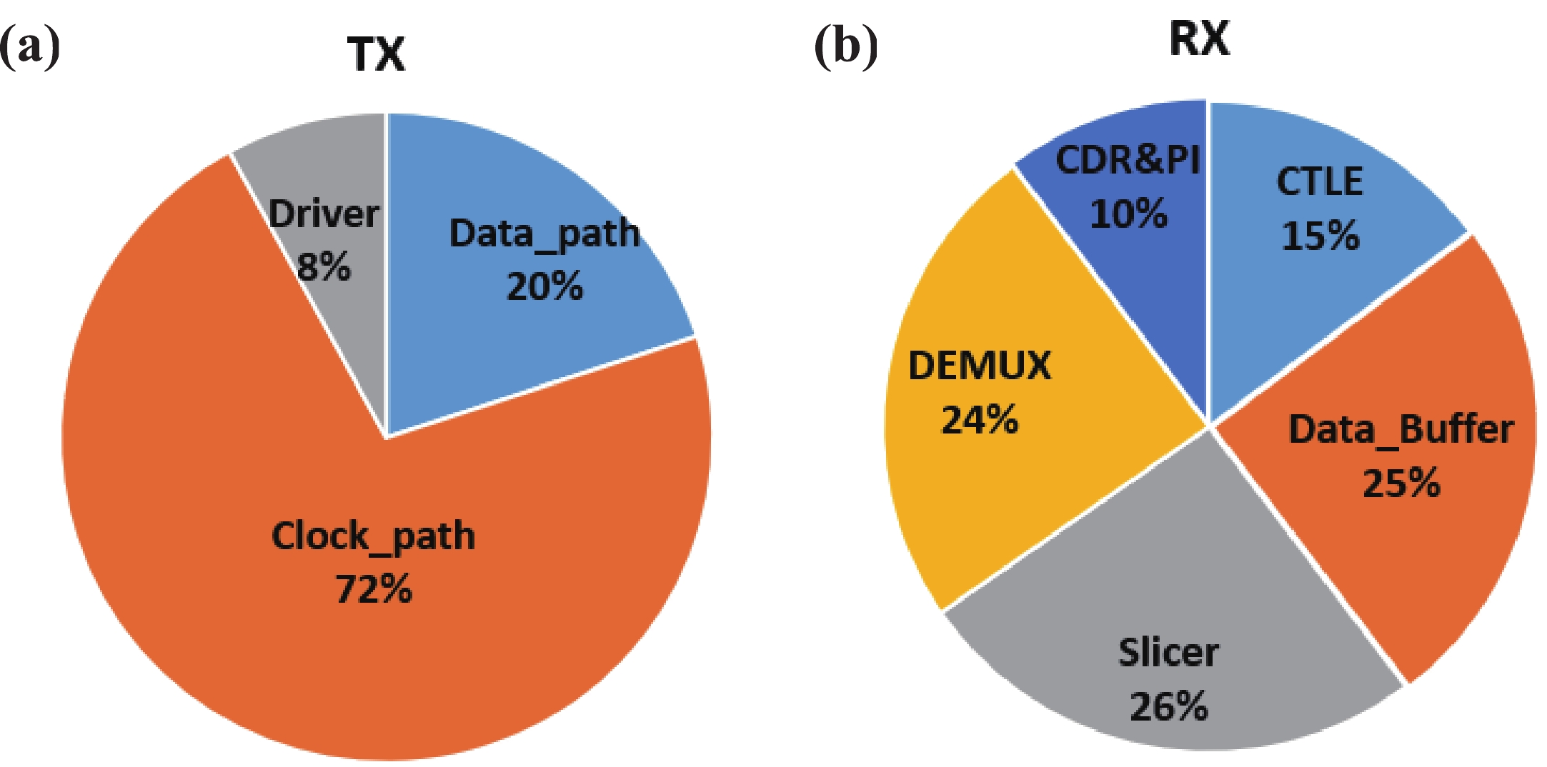
Abstract: A 28/56 Gb/s NRZ/PAM-4 dual-mode transceiver (TRx) designed in a 28-nm complementary metal-oxide-semiconductor (CMOS) process is presented in this article. A voltage-mode (VM) driver featuring a 4-tap reconfigurable feed-forward equalizer (FFE) is employed in the quarter-rate transmitter (TX). The half-rate receiver (RX) incorporates a continuous-time linear equalizer (CTLE), a 3-stage high-speed slicer with multi-clock-phase sampling, and a clock and data recovery (CDR). The experimental results show that the TRx operates at a maximum speed of 56 Gb/s with chip-on board (COB) assembly. The 28 Gb/s NRZ eye diagram shows a far-end vertical eye opening of 210 mV with an output amplitude of 351 mV single-ended and the 56 Gb/s PAM-4 eye diagram exhibits far-end eye opening of 33 mV (upper-eye), 31 mV (mid-eye), and 28 mV (lower-eye) with an output amplitude of 353 mV single-ended. The recovered 14 GHz clock from the RX exhibits random jitter (RJ) of 469 fs and deterministic jitter (DJ) of 8.76 ps. The 875 Mb/s de-multiplexed data features 593 ps horizontal eye opening with 32.02 ps RJ, at bit-error rate (BER) of 10−5 (0.53 UI). The power dissipation of TX and RX are 125 and 181.4 mW, respectively, from a 0.9-V supply.
Keywords: transceiver (TRx), feed-forward equalizer (FFE), clock and data recovery (CDR), continuous time linear equalizer (CTLE)
| [1] |
Kim D, Park M, Jang S, et al. A 1.1 V 1ynm 6.4Gb/s/pin 16Gb DDR5 SDRAM with a phase-rotator-based DLL, high-speed SerDes and RX/TX equalization scheme. IEEE International Solid-State Circuits Conference, 2019, 380 doi: 10.1109/ISSCC.2019.8662320
|
| [2] |
Pan Q, Luo X S, Li Z H, et al. A 26-Gb/s CMOS optical receiver with a reference-less CDR in 65-nm CMOS. J Semicond, 2022, 43, 072401 doi: 10.1088/1674-4926/43/7/072401
|
| [3] |
Optical Internetworking Forum. Common electrical I/O (CEI) electrical and jitter interoperability agreements for 6G+ bps, 11G+ bps and 25G+ bps I/O. [Online]. Available: http://www.oiforum.com
|
| [4] |
IEEE P802.3 bs 200 Gb/s and 400 Gb/s Ethernet Task Force, accessed on Nov. 2016. [Online]. Available: http://www.ieee802.org
|
| [5] |
Liao Q W, Zhang Y G, Ma S Y, et al. A 50-Gb/s PAM-4 silicon-photonic transmitter incorporating lumped-segment MZM, distributed CMOS driver, and integrated CDR. IEEE J Solid-State Circuits, 2022, 57, 767 doi: 10.1109/JSSC.2021.3134874
|
| [6] |
Lee J, Chiang P C, Peng P J, et al. Design of 56 gb/s NRZ and PAM4 SerDes transceivers in CMOS technologies. IEEE J Solid-State Circuits, 2015, 50, 2061 doi: 10.1109/JSSC.2015.2433269
|
| [7] |
Im J, Freitas D, Roldan A B, et al. A 40-to-56 Gb/s PAM-4 receiver with ten-tap direct decision-feedback equalization in 16-nm FinFET. IEEE J Solid-State Circuits, 2017, 52, 3486 doi: 10.1109/JSSC.2017.2749432
|
| [8] |
Frans Y, Shin J, Zhou L, et al. A 56-gb/s PAM4 wireline transceiver using a 32-way time-interleaved SAR ADC in 16-nm FinFET. IEEE J Solid-State Circuits, 2017, 52, 1101 doi: 10.1109/JSSC.2016.2632300
|
| [9] |
Wang L K, Fu Y Y, LaCroix M, et al. A 64Gb/s PAM-4 transceiver utilizing an adaptive threshold ADC in 16nm FinFET. IEEE International Solid-State Circuits Conference, 2018, 110 doi: 10.1109/ISSCC.2018.8310208
|
| [10] |
Kocaman N, Singh U, Raghavan B, et al. An 182mW 1-60Gb/s configurable PAM-4/NRZ transceiver for large scale ASIC integration in 7nm FinFET technology. IEEE International Solid-State Circuits Conference, 2022, 120 doi: 10.1109/ISSCC42614.2022.9731688
|
| [11] |
Upadhyaya P, Poon C F, Lim S W, et al. A fully adaptive 19-to-56Gb/s PAM-4 wireline transceiver with a configurable ADC in 16nm FinFET. IEEE International Solid-State Circuits Conference, 2018, 108 doi: 10.1109/ISSCC.2018.8310207
|
| [12] |
Gopalakrishnan K, Ren A L, Tan A, et al. A 40/50/100Gb/s PAM-4 Ethernet transceiver in 28nm CMOS. IEEE International Solid-State Circuits Conference, 2016, 62 doi: 10.1109/ISSCC.2016.7417907
|
| [13] |
Depaoli E, Zhang H Y, Mazzini M, et al. A 64 Gb/s low-power transceiver for short-reach PAM-4 electrical links in 28-nm FDSOI CMOS. IEEE J Solid-State Circuits, 2019, 54, 6 doi: 10.1109/JSSC.2018.2873602
|
| [14] |
Peng P J, Li J F, Chen L Y, et al. A 56 Gb/s PAM-4/NRZ transceiver in 40 nm CMOS. IEEE International Solid-State Circuits Conference, 2017, 110 doi: 10.1109/ISSCC.2017.7870285
|
| [15] |
He Y K, Yuan Z, Wang K N, et al. A 28/56 Gb/s NRZ/PAM-4 dual-mode transceiver in 28-nm CMOS. 2023 IEEE International Conference on Integrated Circuits, Technologies and Applications, 2023, 138 doi: 10.1109/ICTA60488.2023.10364301
|
| [16] |
Dickson T O, Ainspan H A, Meghelli M. A 1.8pJ/b 56Gb/s PAM-4 transmitter with fractionally spaced FFE in 14nm CMOS. IEEE International Solid-State Circuits Conference, 2017, 118 doi: 10.1109/ISSCC.2017.7870289
|
| [17] |
Roshan-Zamir A, Elhadidy O, Yang H W, et al. A reconfigurable 16/32 Gb/s dual-mode NRZ/PAM4 SerDes in 65-nm CMOS. IEEE J Solid-State Circuits, 2017, 52, 2430 doi: 10.1109/JSSC.2017.2705070
|
| [18] |
Roshan-Zamir A, Iwai T, Fan Y H, et al. A 56-Gb/s PAM4 receiver with low-overhead techniques for threshold and edge-based DFE FIR- and IIR-tap adaptation in 65-nm CMOS. IEEE J Solid-State Circuits, 2019, 54, 672 doi: 10.1109/JSSC.2018.2881278
|
| [19] |
Kim J, Balankutty A, Dokania R, et al. A 112 Gb/s PAM-4 transmitter with 3-Tap FFE in 10 nm CMOS. IEEE International Solid-State Circuits Conference, 2018, 102 doi: 10.1109/ISSCC.2018.8310204
|
| [20] |
Menolfi C, Braendli M, Francese P A, et al. A 112 Gb/S 2.6 pJ/b 8-tap FFE PAM-4 SST TX in 14 nm CMOS. IEEE International Solid-State Circuits Conference, 2018, 104 doi: 10.1109/ISSCC.2018.8310205
|
| [21] |
Razavi B. Jitter-power trade-offs in PLLs. IEEE Transactions on Circuits and Systems I, 2021, 68, 1381 doi: 10.1109/TCSI.2021.3057580
|
| [22] |
Toprak-Deniz Z, Proesel J E, Bulzacchelli J F, et al. A 128Gb/s 1.3pJ/b PAM-4 transmitter with reconfigurable 3-tap FFE in 14nm CMOS. 2019 IEEE International Solid-State Circuits Conference, 2019, 122 doi: 10.1109/ISSCC.2019.8662479
|
| [23] |
Lin Y T, Chen W Z. A 50 Gb/s PAM-4 transmitter with feedforward equalizer and background phase error calibration. IEEE Asian Solid-State Circuits Conference, 2020, 1 doi: 10.1109/A-SSCC48613.2020.9336134
|
| [24] |
Tang R J, Yuan Z, Lv Y Y, et al. A continuous-time linear equalizer with ultrafine gain adjustment achieving 0.3-dB DC-gain step and 0.9-dB peaking-gain step. IEEE Microw Wirel Technol Lett, 2023, 33, 559 doi: 10.1109/LMWT.2022.3233634
|
| [25] |
Chen K C, Kuo W W T, Emami A. A 60-gb/s PAM4 wireline receiver with 2-tap direct decision feedback equalization employing track-and-regenerate slicers in 28-nm CMOS. IEEE J Solid-State Circuits, 2021, 56, 750 doi: 10.1109/JSSC.2020.3025285
|
| [26] |
Yeom S, Sim T, Han J. An analysis of CMOS latched comparators. International Conference on Electronics, Information, and Communication, 2023, 1 doi: 10.1109/ICEIC57457.2023.10049873
|
| [27] |
Günay R, Ergün S. IC random number generator exploiting two simultaneous metastable events of tetrahedral oscillators. IEEE Trans Circuits Syst II Express Briefs, 2020, 67, 1634 doi: 10.1109/TCSII.2020.3012869
|
| [28] |
Smith R L, Lee T H. Analysis and design of a tetrahedral oscillator. IEEE Trans Circuits Syst II Express Briefs, 2022, 69, 75 doi: 10.1109/TCSII.2021.3097100
|
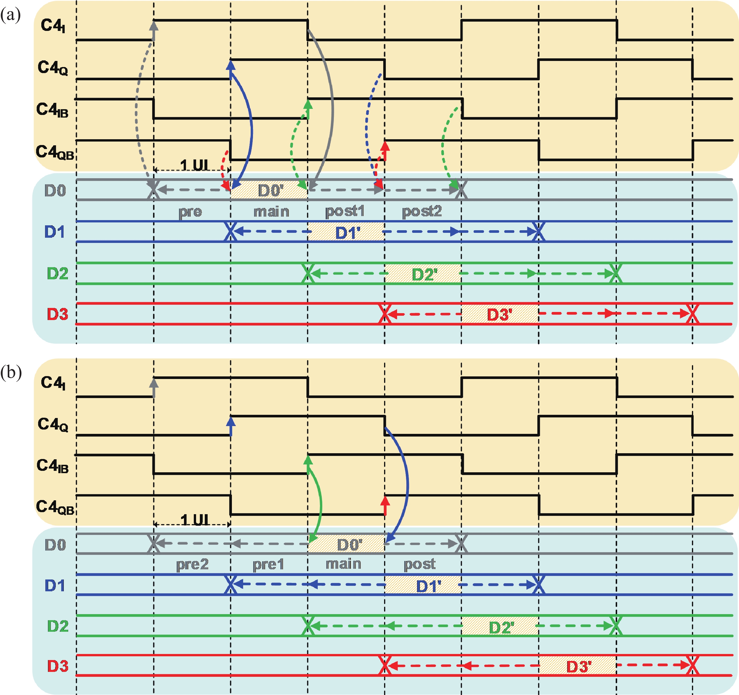
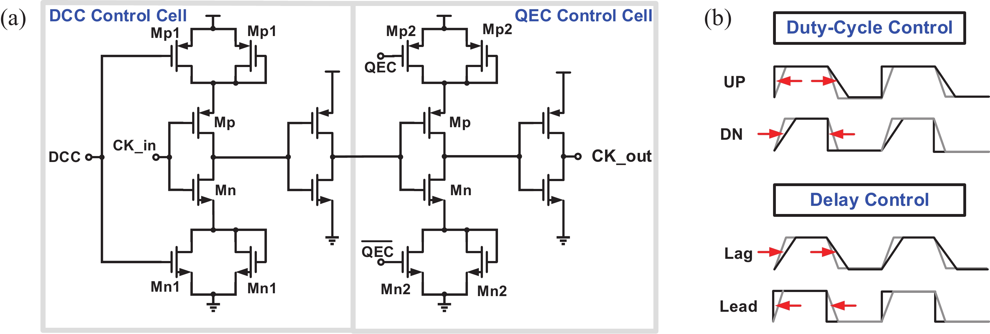
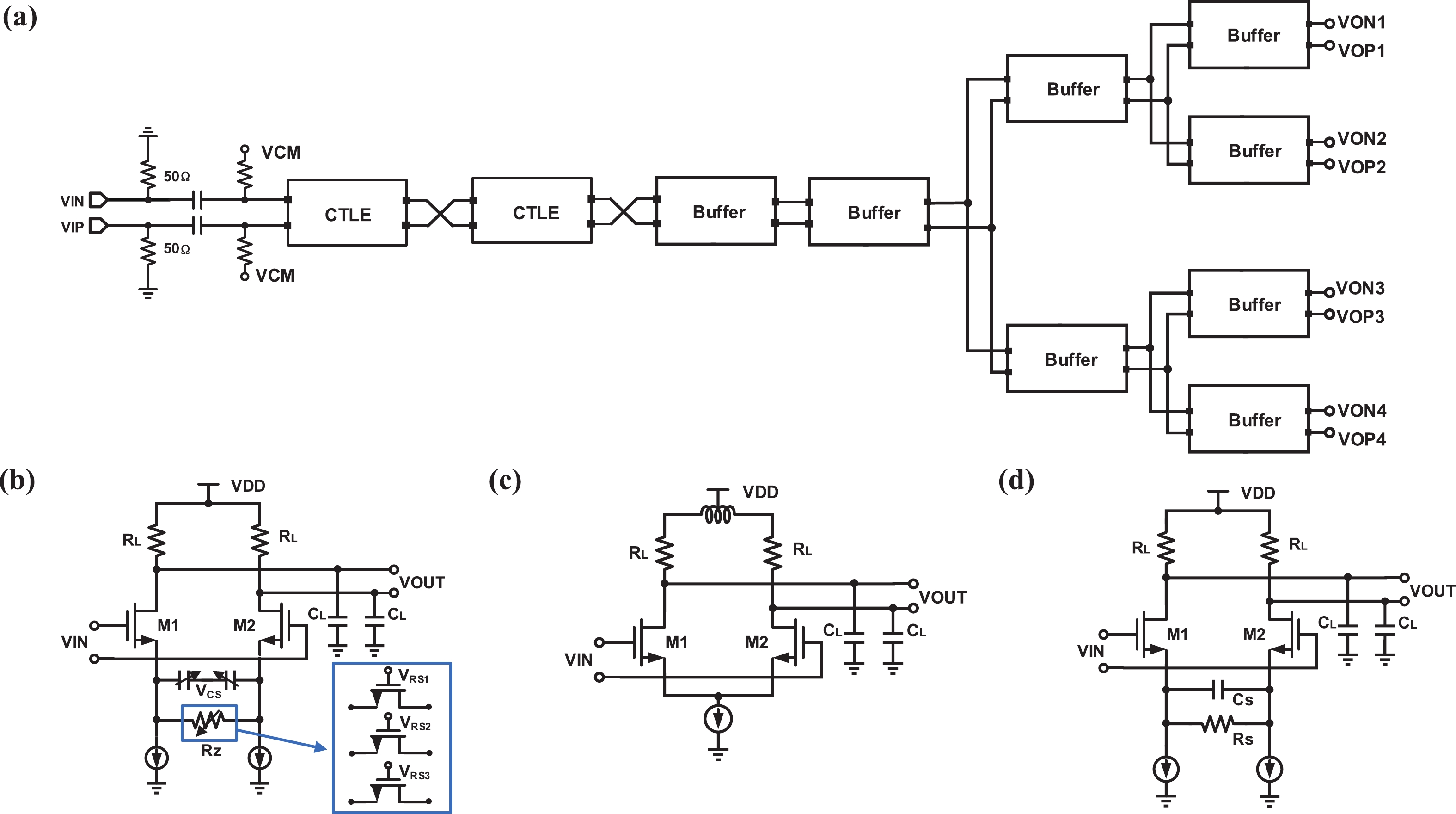
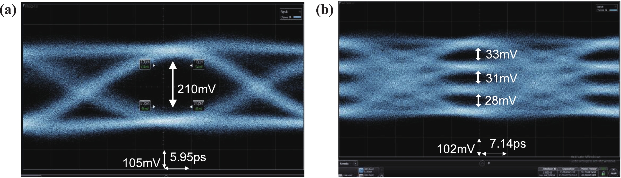
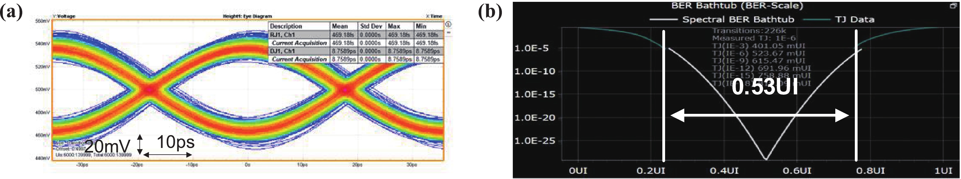
Table 1. Performance summary and comparison.
| Parameters | Ref. [4] | Ref. [6] | Ref. [7] | Ref. [8] | This work | |||||
| Data rate (Gb/s) | 56 | 56 | 64.375 | 60 | 56 | |||||
| Technology | 40-nm CMOS | 16-nm FinFET | 16-nm FinFET | 7-nm FinFET | 28-nm CMOS | |||||
| Architecture | Mixed-signal | ADC-DSP | ADC-DSP | ADC-DSP | Mixed-signal | |||||
| Active area (mm2) | TX:1.14 RX:1.6 | N/A | TX:0.09 RX:0.163 | 0.268 | TX:0.115 RX:0.532 | |||||
| Power (mW) | TX:290 RX:420 | TX:140 RX:370 | TX:89.7 RX:100 | 182 | TX:125 RX:181.4 | |||||
| Link power efficiency (pJ/bit) | 12.679 | 9.1 (w/o DSP) | 2.95 (w/o DSP) | 3.03 (w/DSP) | 5.47 | |||||
| Recovered clock jitterRMS (fs) | 520 | N/A | N/A | N/A | 469 |
 DownLoad: CSV
| [1] |
Kim D, Park M, Jang S, et al. A 1.1 V 1ynm 6.4Gb/s/pin 16Gb DDR5 SDRAM with a phase-rotator-based DLL, high-speed SerDes and RX/TX equalization scheme. IEEE International Solid-State Circuits Conference, 2019, 380 doi: 10.1109/ISSCC.2019.8662320
|
| [2] |
Pan Q, Luo X S, Li Z H, et al. A 26-Gb/s CMOS optical receiver with a reference-less CDR in 65-nm CMOS. J Semicond, 2022, 43, 072401 doi: 10.1088/1674-4926/43/7/072401
|
| [3] |
Optical Internetworking Forum. Common electrical I/O (CEI) electrical and jitter interoperability agreements for 6G+ bps, 11G+ bps and 25G+ bps I/O. [Online]. Available: http://www.oiforum.com
|
| [4] |
IEEE P802.3 bs 200 Gb/s and 400 Gb/s Ethernet Task Force, accessed on Nov. 2016. [Online]. Available: http://www.ieee802.org
|
| [5] |
Liao Q W, Zhang Y G, Ma S Y, et al. A 50-Gb/s PAM-4 silicon-photonic transmitter incorporating lumped-segment MZM, distributed CMOS driver, and integrated CDR. IEEE J Solid-State Circuits, 2022, 57, 767 doi: 10.1109/JSSC.2021.3134874
|
| [6] |
Lee J, Chiang P C, Peng P J, et al. Design of 56 gb/s NRZ and PAM4 SerDes transceivers in CMOS technologies. IEEE J Solid-State Circuits, 2015, 50, 2061 doi: 10.1109/JSSC.2015.2433269
|
| [7] |
Im J, Freitas D, Roldan A B, et al. A 40-to-56 Gb/s PAM-4 receiver with ten-tap direct decision-feedback equalization in 16-nm FinFET. IEEE J Solid-State Circuits, 2017, 52, 3486 doi: 10.1109/JSSC.2017.2749432
|
| [8] |
Frans Y, Shin J, Zhou L, et al. A 56-gb/s PAM4 wireline transceiver using a 32-way time-interleaved SAR ADC in 16-nm FinFET. IEEE J Solid-State Circuits, 2017, 52, 1101 doi: 10.1109/JSSC.2016.2632300
|
| [9] |
Wang L K, Fu Y Y, LaCroix M, et al. A 64Gb/s PAM-4 transceiver utilizing an adaptive threshold ADC in 16nm FinFET. IEEE International Solid-State Circuits Conference, 2018, 110 doi: 10.1109/ISSCC.2018.8310208
|
| [10] |
Kocaman N, Singh U, Raghavan B, et al. An 182mW 1-60Gb/s configurable PAM-4/NRZ transceiver for large scale ASIC integration in 7nm FinFET technology. IEEE International Solid-State Circuits Conference, 2022, 120 doi: 10.1109/ISSCC42614.2022.9731688
|
| [11] |
Upadhyaya P, Poon C F, Lim S W, et al. A fully adaptive 19-to-56Gb/s PAM-4 wireline transceiver with a configurable ADC in 16nm FinFET. IEEE International Solid-State Circuits Conference, 2018, 108 doi: 10.1109/ISSCC.2018.8310207
|
| [12] |
Gopalakrishnan K, Ren A L, Tan A, et al. A 40/50/100Gb/s PAM-4 Ethernet transceiver in 28nm CMOS. IEEE International Solid-State Circuits Conference, 2016, 62 doi: 10.1109/ISSCC.2016.7417907
|
| [13] |
Depaoli E, Zhang H Y, Mazzini M, et al. A 64 Gb/s low-power transceiver for short-reach PAM-4 electrical links in 28-nm FDSOI CMOS. IEEE J Solid-State Circuits, 2019, 54, 6 doi: 10.1109/JSSC.2018.2873602
|
| [14] |
Peng P J, Li J F, Chen L Y, et al. A 56 Gb/s PAM-4/NRZ transceiver in 40 nm CMOS. IEEE International Solid-State Circuits Conference, 2017, 110 doi: 10.1109/ISSCC.2017.7870285
|
| [15] |
He Y K, Yuan Z, Wang K N, et al. A 28/56 Gb/s NRZ/PAM-4 dual-mode transceiver in 28-nm CMOS. 2023 IEEE International Conference on Integrated Circuits, Technologies and Applications, 2023, 138 doi: 10.1109/ICTA60488.2023.10364301
|
| [16] |
Dickson T O, Ainspan H A, Meghelli M. A 1.8pJ/b 56Gb/s PAM-4 transmitter with fractionally spaced FFE in 14nm CMOS. IEEE International Solid-State Circuits Conference, 2017, 118 doi: 10.1109/ISSCC.2017.7870289
|
| [17] |
Roshan-Zamir A, Elhadidy O, Yang H W, et al. A reconfigurable 16/32 Gb/s dual-mode NRZ/PAM4 SerDes in 65-nm CMOS. IEEE J Solid-State Circuits, 2017, 52, 2430 doi: 10.1109/JSSC.2017.2705070
|
| [18] |
Roshan-Zamir A, Iwai T, Fan Y H, et al. A 56-Gb/s PAM4 receiver with low-overhead techniques for threshold and edge-based DFE FIR- and IIR-tap adaptation in 65-nm CMOS. IEEE J Solid-State Circuits, 2019, 54, 672 doi: 10.1109/JSSC.2018.2881278
|
| [19] |
Kim J, Balankutty A, Dokania R, et al. A 112 Gb/s PAM-4 transmitter with 3-Tap FFE in 10 nm CMOS. IEEE International Solid-State Circuits Conference, 2018, 102 doi: 10.1109/ISSCC.2018.8310204
|
| [20] |
Menolfi C, Braendli M, Francese P A, et al. A 112 Gb/S 2.6 pJ/b 8-tap FFE PAM-4 SST TX in 14 nm CMOS. IEEE International Solid-State Circuits Conference, 2018, 104 doi: 10.1109/ISSCC.2018.8310205
|
| [21] |
Razavi B. Jitter-power trade-offs in PLLs. IEEE Transactions on Circuits and Systems I, 2021, 68, 1381 doi: 10.1109/TCSI.2021.3057580
|
| [22] |
Toprak-Deniz Z, Proesel J E, Bulzacchelli J F, et al. A 128Gb/s 1.3pJ/b PAM-4 transmitter with reconfigurable 3-tap FFE in 14nm CMOS. 2019 IEEE International Solid-State Circuits Conference, 2019, 122 doi: 10.1109/ISSCC.2019.8662479
|
| [23] |
Lin Y T, Chen W Z. A 50 Gb/s PAM-4 transmitter with feedforward equalizer and background phase error calibration. IEEE Asian Solid-State Circuits Conference, 2020, 1 doi: 10.1109/A-SSCC48613.2020.9336134
|
| [24] |
Tang R J, Yuan Z, Lv Y Y, et al. A continuous-time linear equalizer with ultrafine gain adjustment achieving 0.3-dB DC-gain step and 0.9-dB peaking-gain step. IEEE Microw Wirel Technol Lett, 2023, 33, 559 doi: 10.1109/LMWT.2022.3233634
|
| [25] |
Chen K C, Kuo W W T, Emami A. A 60-gb/s PAM4 wireline receiver with 2-tap direct decision feedback equalization employing track-and-regenerate slicers in 28-nm CMOS. IEEE J Solid-State Circuits, 2021, 56, 750 doi: 10.1109/JSSC.2020.3025285
|
| [26] |
Yeom S, Sim T, Han J. An analysis of CMOS latched comparators. International Conference on Electronics, Information, and Communication, 2023, 1 doi: 10.1109/ICEIC57457.2023.10049873
|
| [27] |
Günay R, Ergün S. IC random number generator exploiting two simultaneous metastable events of tetrahedral oscillators. IEEE Trans Circuits Syst II Express Briefs, 2020, 67, 1634 doi: 10.1109/TCSII.2020.3012869
|
| [28] |
Smith R L, Lee T H. Analysis and design of a tetrahedral oscillator. IEEE Trans Circuits Syst II Express Briefs, 2022, 69, 75 doi: 10.1109/TCSII.2021.3097100
|


Article views: 3614 Times PDF downloads: 544 Times Cited by: 0 Times
Received: 12 January 2024 Revised: 09 April 2024 Online: Accepted Manuscript: 26 April 2024Uncorrected proof: 26 April 2024Published: 15 June 2024
| Citation: |
Yukun He, Zhao Yuan, Kanan Wang, Renjie Tang, Yunxiang He, Xian Chen, Zhengyang Ye, Xiaoyan Gui. A 28/56 Gb/s NRZ/PAM-4 dual-mode transceiver with 1/4 rate reconfigurable 4-tap FFE and half-rate slicer in a 28-nm CMOS[J]. Journal of Semiconductors, 2024, 45(6): 062204. doi: 10.1088/1674-4926/24010001
****
Y K He, Z Yuan, K N Wang, R J Tang, Y X He, X Chen, Z Y Ye, and X Y Gui, A 28/56 Gb/s NRZ/PAM-4 dual-mode transceiver with 1/4 rate reconfigurable 4-tap FFE and half-rate slicer in a 28-nm CMOS[J]. J. Semicond., 2024, 45(6), 062204 doi: 10.1088/1674-4926/24010001

|
 Yukun He received his B.S. from Xidian University in 2017. He is currently working toward a Ph.D. degree at Xi’an Jiaotong University. His research interests include high-speed wireline communications and optical communications
 Xiaoyan Gui received his Ph.D. degree from University of California, Irvine, in 2011. He was with Broadcom, Irvine, from 2008 to 2012 where he worked on high-speed SerDes transceiver design as a design engineer and staff scientist. In 2012 he joined the faculty in School of Information and Electronics at Beijing Institute of Technology and later in 2017 the faculty in School of Microelectronics at Xi’an Jiaotong University where he is currently Professor. Dr. Gui’s research covers CMOS high-speed broad-band communication (Wireline) and radio-frequency (RF)/mili-meter wave (mmW) IC design. He is the author of more than 50 journal and conference papers. He is a senior member of IEEE
| [1] |
Kim D, Park M, Jang S, et al. A 1.1 V 1ynm 6.4Gb/s/pin 16Gb DDR5 SDRAM with a phase-rotator-based DLL, high-speed SerDes and RX/TX equalization scheme. IEEE International Solid-State Circuits Conference, 2019, 380 doi: 10.1109/ISSCC.2019.8662320
|
| [2] |
Pan Q, Luo X S, Li Z H, et al. A 26-Gb/s CMOS optical receiver with a reference-less CDR in 65-nm CMOS. J Semicond, 2022, 43, 072401 doi: 10.1088/1674-4926/43/7/072401
|
| [3] |
Optical Internetworking Forum. Common electrical I/O (CEI) electrical and jitter interoperability agreements for 6G+ bps, 11G+ bps and 25G+ bps I/O. [Online]. Available: http://www.oiforum.com
|
| [4] |
IEEE P802.3 bs 200 Gb/s and 400 Gb/s Ethernet Task Force, accessed on Nov. 2016. [Online]. Available: http://www.ieee802.org
|
| [5] |
Liao Q W, Zhang Y G, Ma S Y, et al. A 50-Gb/s PAM-4 silicon-photonic transmitter incorporating lumped-segment MZM, distributed CMOS driver, and integrated CDR. IEEE J Solid-State Circuits, 2022, 57, 767 doi: 10.1109/JSSC.2021.3134874
|
| [6] |
Lee J, Chiang P C, Peng P J, et al. Design of 56 gb/s NRZ and PAM4 SerDes transceivers in CMOS technologies. IEEE J Solid-State Circuits, 2015, 50, 2061 doi: 10.1109/JSSC.2015.2433269
|
| [7] |
Im J, Freitas D, Roldan A B, et al. A 40-to-56 Gb/s PAM-4 receiver with ten-tap direct decision-feedback equalization in 16-nm FinFET. IEEE J Solid-State Circuits, 2017, 52, 3486 doi: 10.1109/JSSC.2017.2749432
|
| [8] |
Frans Y, Shin J, Zhou L, et al. A 56-gb/s PAM4 wireline transceiver using a 32-way time-interleaved SAR ADC in 16-nm FinFET. IEEE J Solid-State Circuits, 2017, 52, 1101 doi: 10.1109/JSSC.2016.2632300
|
| [9] |
Wang L K, Fu Y Y, LaCroix M, et al. A 64Gb/s PAM-4 transceiver utilizing an adaptive threshold ADC in 16nm FinFET. IEEE International Solid-State Circuits Conference, 2018, 110 doi: 10.1109/ISSCC.2018.8310208
|
| [10] |
Kocaman N, Singh U, Raghavan B, et al. An 182mW 1-60Gb/s configurable PAM-4/NRZ transceiver for large scale ASIC integration in 7nm FinFET technology. IEEE International Solid-State Circuits Conference, 2022, 120 doi: 10.1109/ISSCC42614.2022.9731688
|
| [11] |
Upadhyaya P, Poon C F, Lim S W, et al. A fully adaptive 19-to-56Gb/s PAM-4 wireline transceiver with a configurable ADC in 16nm FinFET. IEEE International Solid-State Circuits Conference, 2018, 108 doi: 10.1109/ISSCC.2018.8310207
|
| [12] |
Gopalakrishnan K, Ren A L, Tan A, et al. A 40/50/100Gb/s PAM-4 Ethernet transceiver in 28nm CMOS. IEEE International Solid-State Circuits Conference, 2016, 62 doi: 10.1109/ISSCC.2016.7417907
|
| [13] |
Depaoli E, Zhang H Y, Mazzini M, et al. A 64 Gb/s low-power transceiver for short-reach PAM-4 electrical links in 28-nm FDSOI CMOS. IEEE J Solid-State Circuits, 2019, 54, 6 doi: 10.1109/JSSC.2018.2873602
|
| [14] |
Peng P J, Li J F, Chen L Y, et al. A 56 Gb/s PAM-4/NRZ transceiver in 40 nm CMOS. IEEE International Solid-State Circuits Conference, 2017, 110 doi: 10.1109/ISSCC.2017.7870285
|
| [15] |
He Y K, Yuan Z, Wang K N, et al. A 28/56 Gb/s NRZ/PAM-4 dual-mode transceiver in 28-nm CMOS. 2023 IEEE International Conference on Integrated Circuits, Technologies and Applications, 2023, 138 doi: 10.1109/ICTA60488.2023.10364301
|
| [16] |
Dickson T O, Ainspan H A, Meghelli M. A 1.8pJ/b 56Gb/s PAM-4 transmitter with fractionally spaced FFE in 14nm CMOS. IEEE International Solid-State Circuits Conference, 2017, 118 doi: 10.1109/ISSCC.2017.7870289
|
| [17] |
Roshan-Zamir A, Elhadidy O, Yang H W, et al. A reconfigurable 16/32 Gb/s dual-mode NRZ/PAM4 SerDes in 65-nm CMOS. IEEE J Solid-State Circuits, 2017, 52, 2430 doi: 10.1109/JSSC.2017.2705070
|
| [18] |
Roshan-Zamir A, Iwai T, Fan Y H, et al. A 56-Gb/s PAM4 receiver with low-overhead techniques for threshold and edge-based DFE FIR- and IIR-tap adaptation in 65-nm CMOS. IEEE J Solid-State Circuits, 2019, 54, 672 doi: 10.1109/JSSC.2018.2881278
|
| [19] |
Kim J, Balankutty A, Dokania R, et al. A 112 Gb/s PAM-4 transmitter with 3-Tap FFE in 10 nm CMOS. IEEE International Solid-State Circuits Conference, 2018, 102 doi: 10.1109/ISSCC.2018.8310204
|
| [20] |
Menolfi C, Braendli M, Francese P A, et al. A 112 Gb/S 2.6 pJ/b 8-tap FFE PAM-4 SST TX in 14 nm CMOS. IEEE International Solid-State Circuits Conference, 2018, 104 doi: 10.1109/ISSCC.2018.8310205
|
| [21] |
Razavi B. Jitter-power trade-offs in PLLs. IEEE Transactions on Circuits and Systems I, 2021, 68, 1381 doi: 10.1109/TCSI.2021.3057580
|
| [22] |
Toprak-Deniz Z, Proesel J E, Bulzacchelli J F, et al. A 128Gb/s 1.3pJ/b PAM-4 transmitter with reconfigurable 3-tap FFE in 14nm CMOS. 2019 IEEE International Solid-State Circuits Conference, 2019, 122 doi: 10.1109/ISSCC.2019.8662479
|
| [23] |
Lin Y T, Chen W Z. A 50 Gb/s PAM-4 transmitter with feedforward equalizer and background phase error calibration. IEEE Asian Solid-State Circuits Conference, 2020, 1 doi: 10.1109/A-SSCC48613.2020.9336134
|
| [24] |
Tang R J, Yuan Z, Lv Y Y, et al. A continuous-time linear equalizer with ultrafine gain adjustment achieving 0.3-dB DC-gain step and 0.9-dB peaking-gain step. IEEE Microw Wirel Technol Lett, 2023, 33, 559 doi: 10.1109/LMWT.2022.3233634
|
| [25] |
Chen K C, Kuo W W T, Emami A. A 60-gb/s PAM4 wireline receiver with 2-tap direct decision feedback equalization employing track-and-regenerate slicers in 28-nm CMOS. IEEE J Solid-State Circuits, 2021, 56, 750 doi: 10.1109/JSSC.2020.3025285
|
| [26] |
Yeom S, Sim T, Han J. An analysis of CMOS latched comparators. International Conference on Electronics, Information, and Communication, 2023, 1 doi: 10.1109/ICEIC57457.2023.10049873
|
| [27] |
Günay R, Ergün S. IC random number generator exploiting two simultaneous metastable events of tetrahedral oscillators. IEEE Trans Circuits Syst II Express Briefs, 2020, 67, 1634 doi: 10.1109/TCSII.2020.3012869
|
| [28] |
Smith R L, Lee T H. Analysis and design of a tetrahedral oscillator. IEEE Trans Circuits Syst II Express Briefs, 2022, 69, 75 doi: 10.1109/TCSII.2021.3097100
|

 WeChat ID
Journal of Semiconductors © 2017 All Rights Reserved 京ICP备05085259号-2