Issue Browser
Volume 46, Issue 3,
Mar 2025

J. Semicond.
2025, 46(3): 031401 doi: 10.1088/1674-4926/24060006
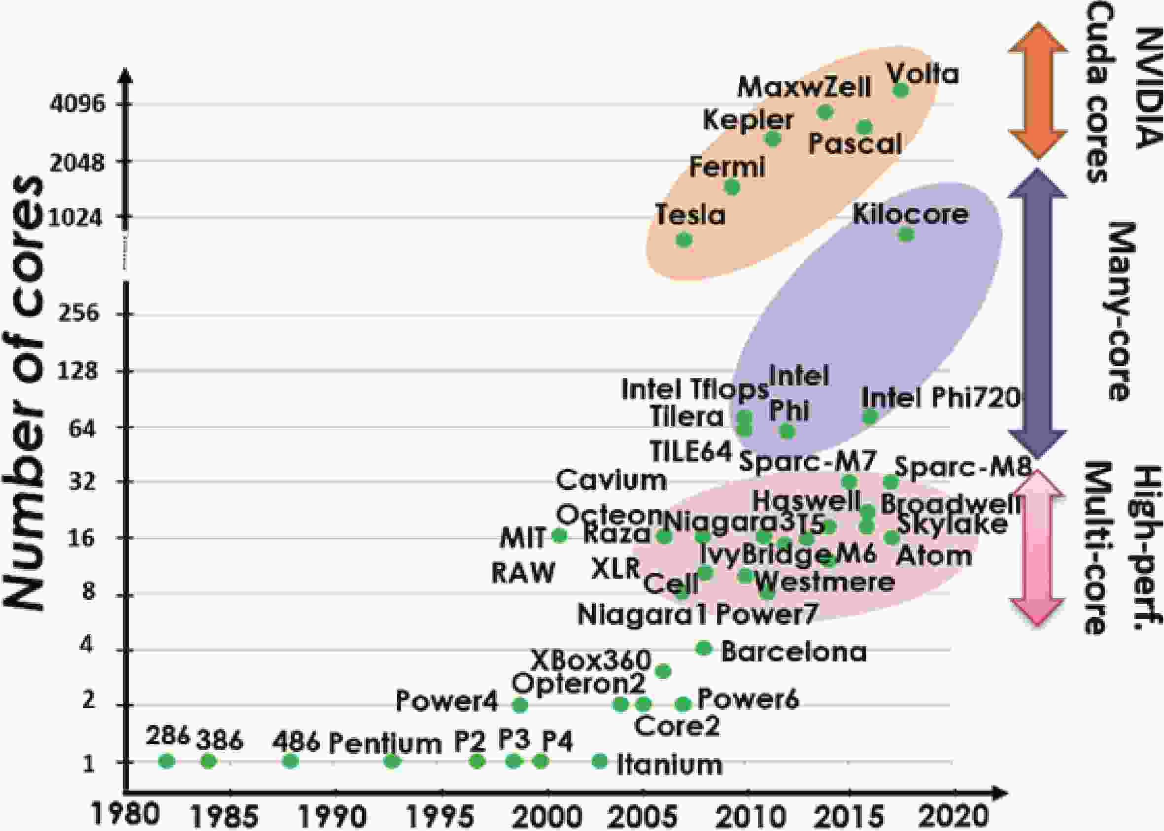
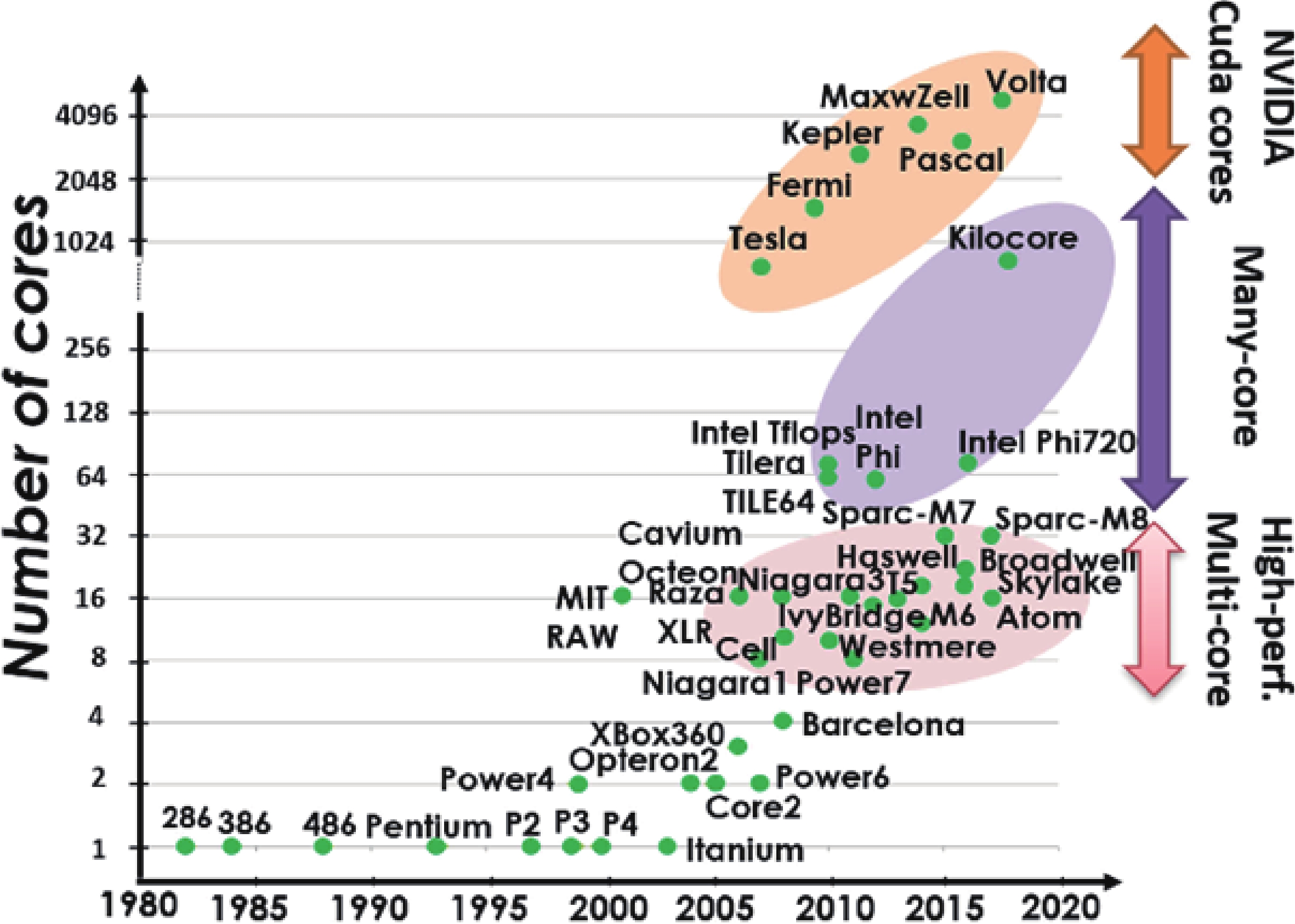
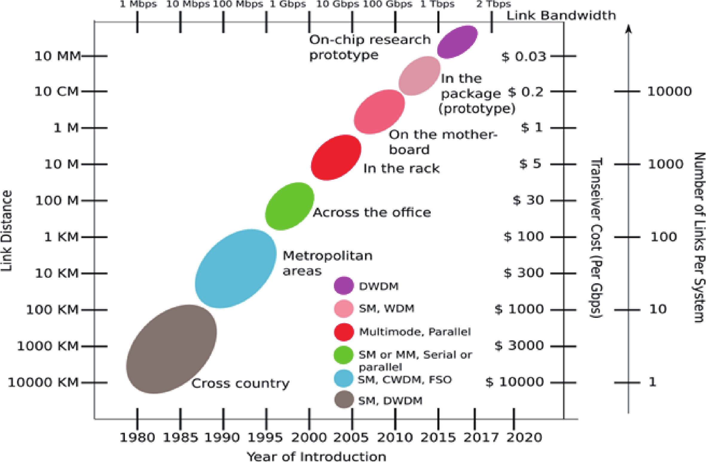
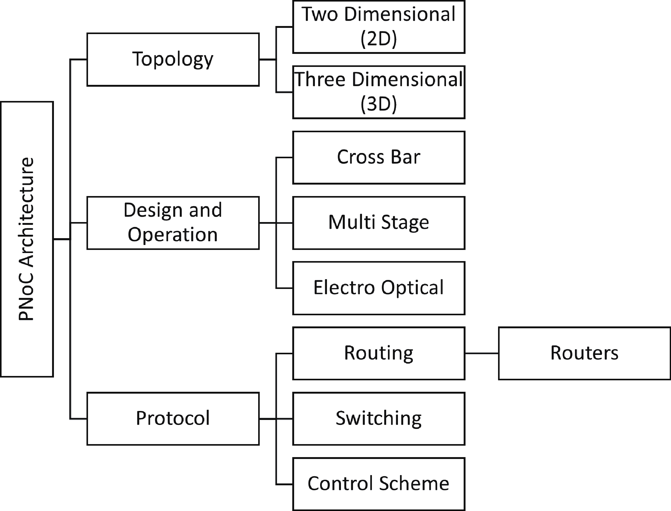
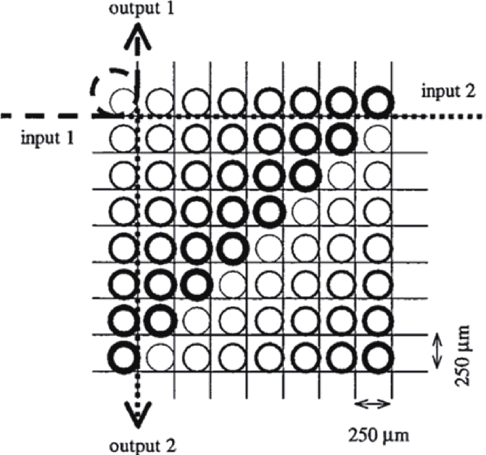
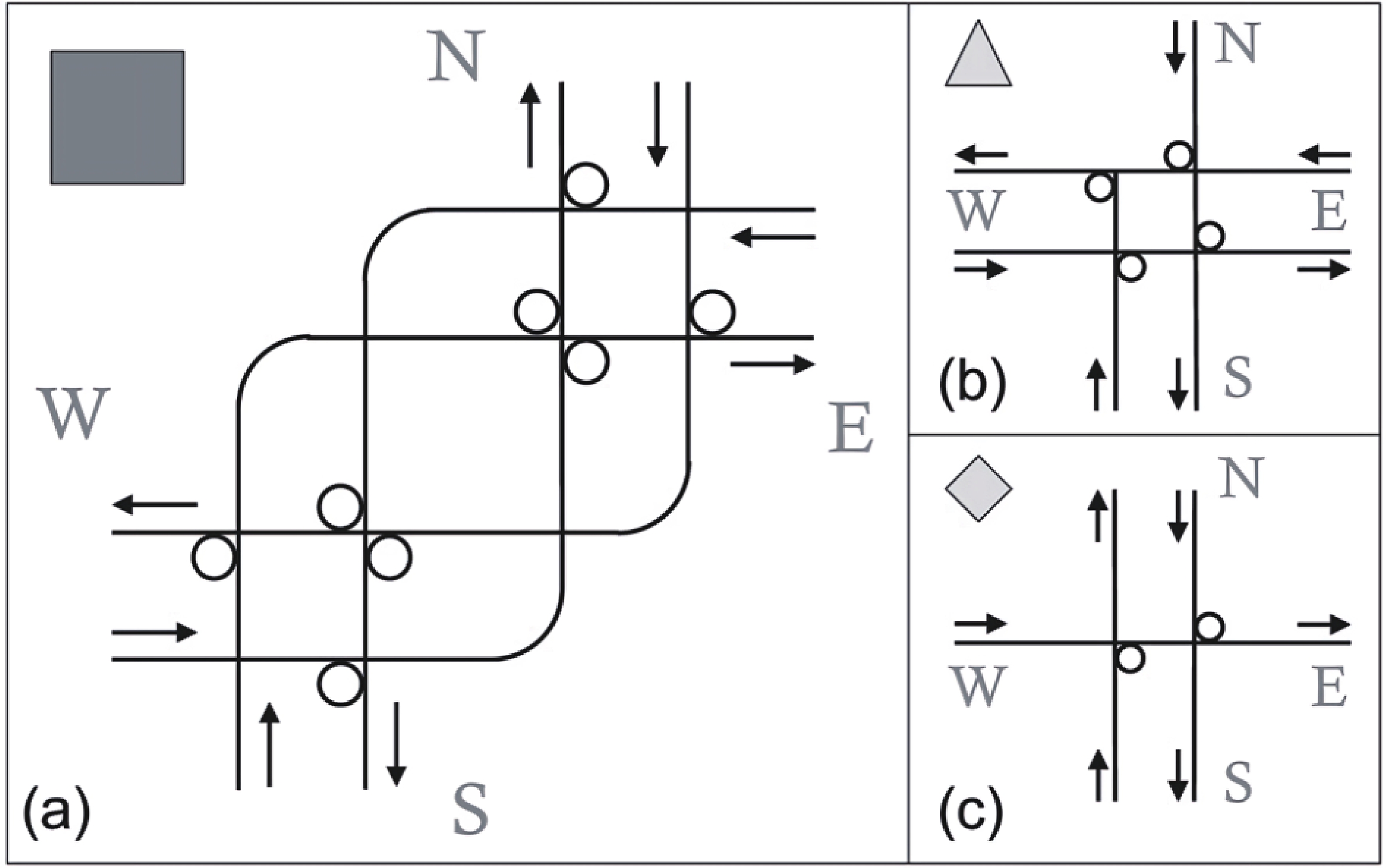
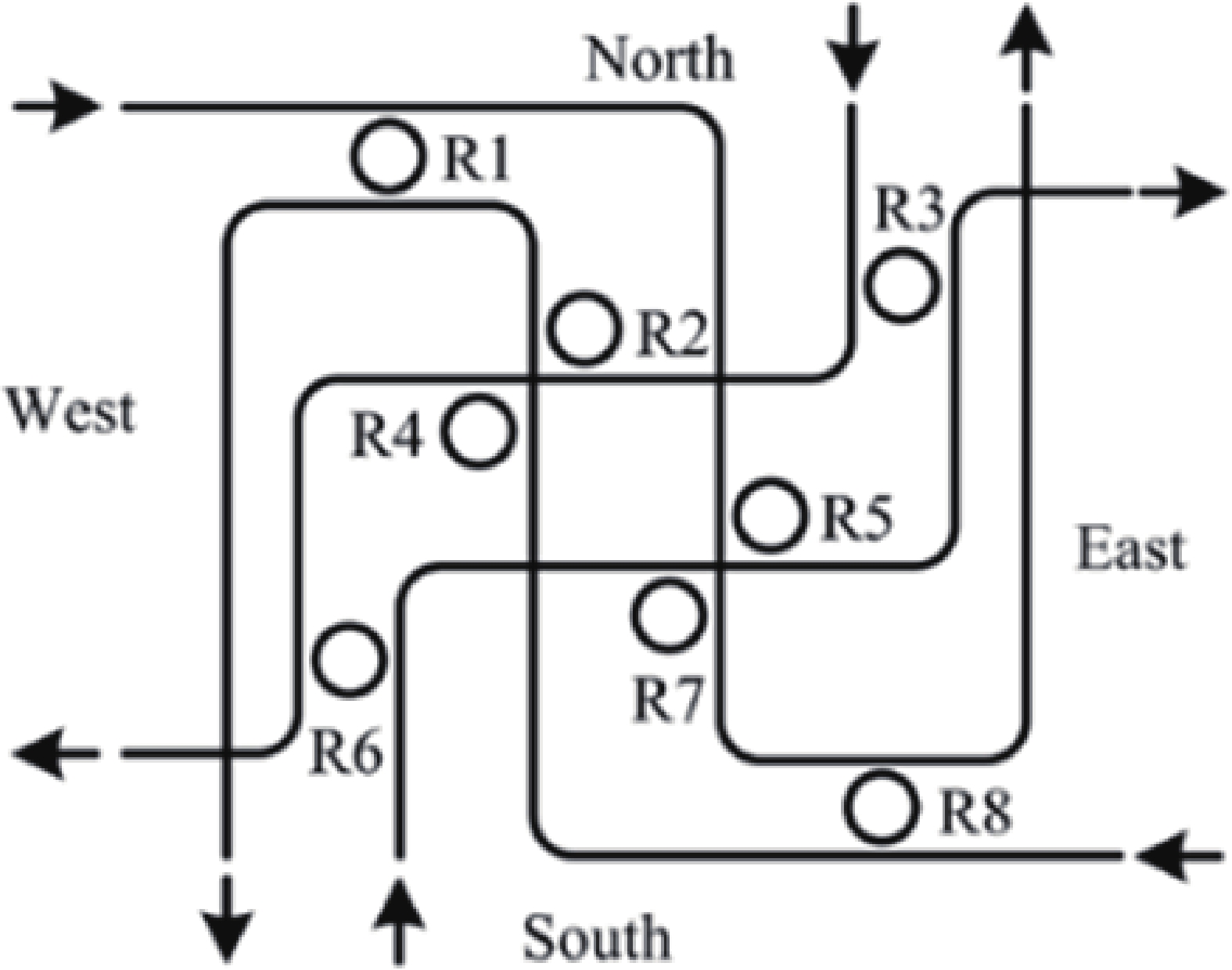
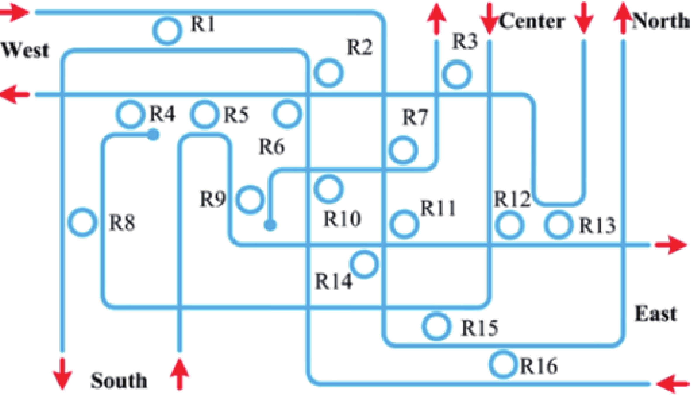
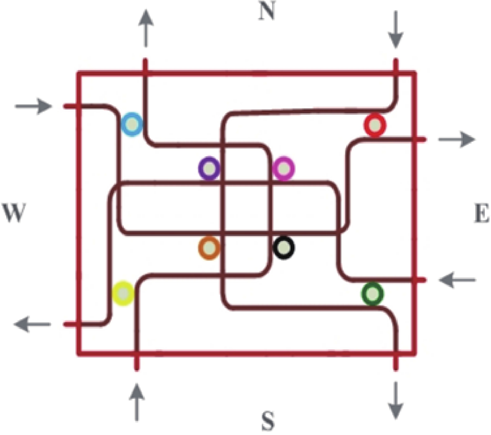
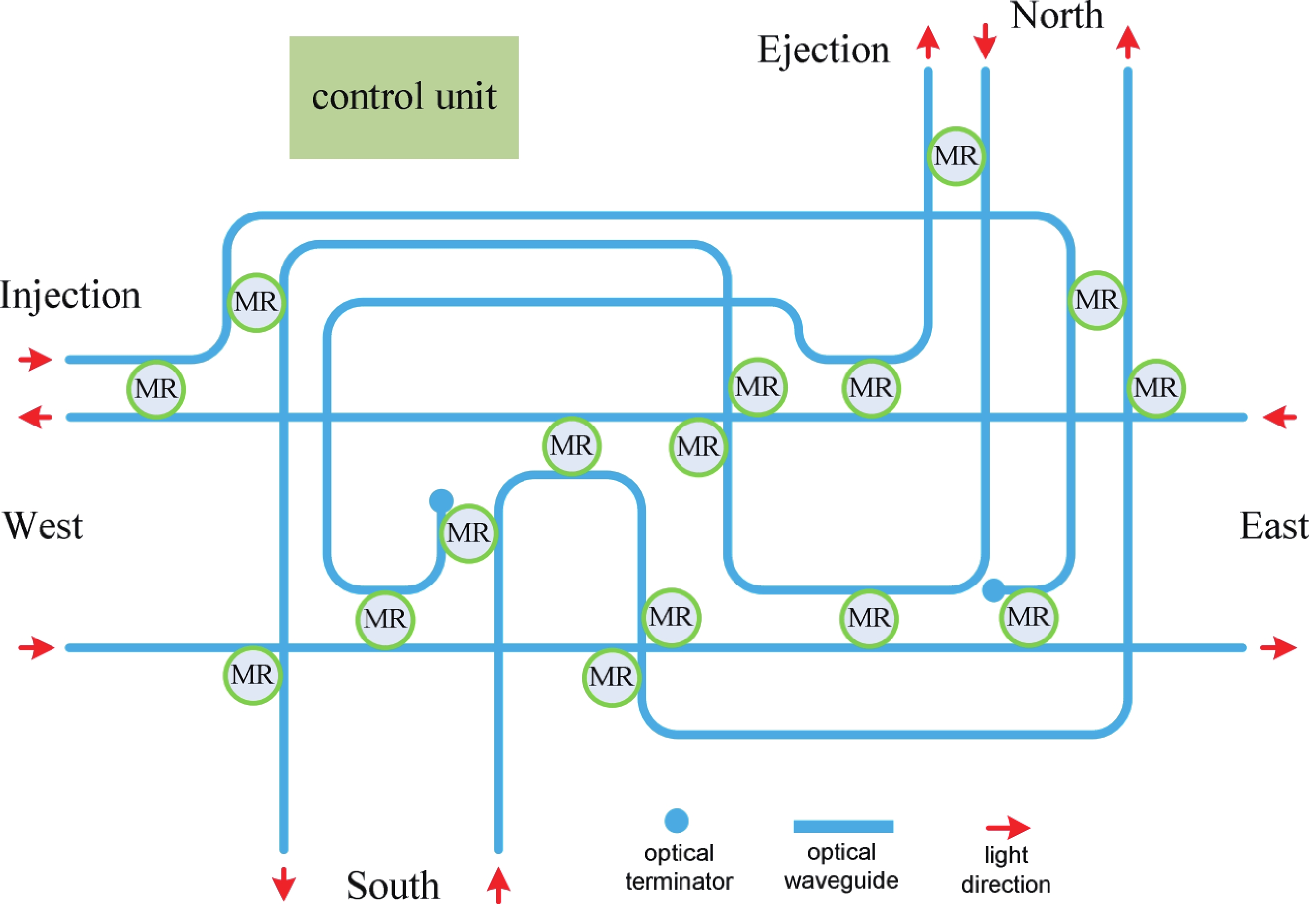
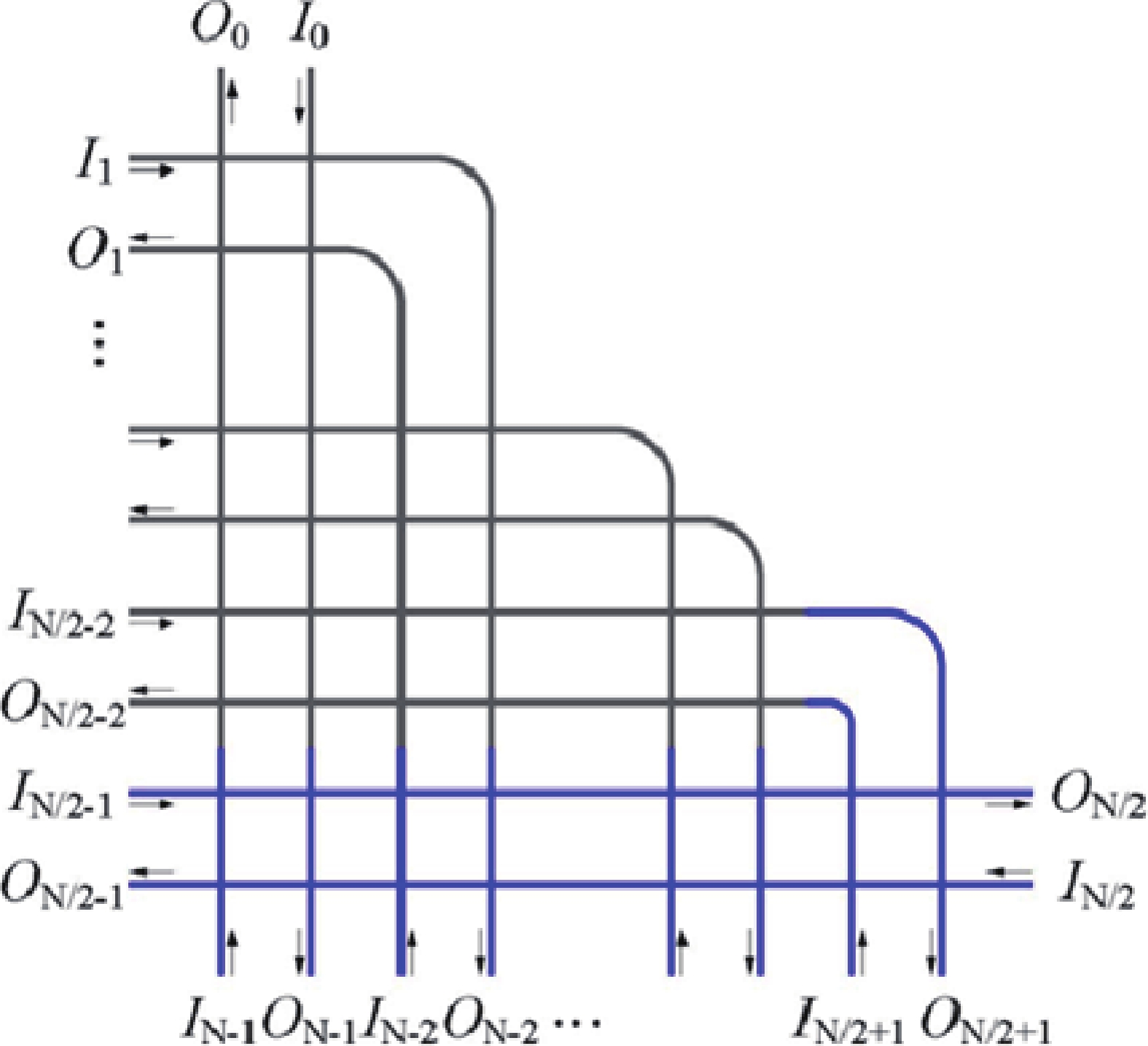
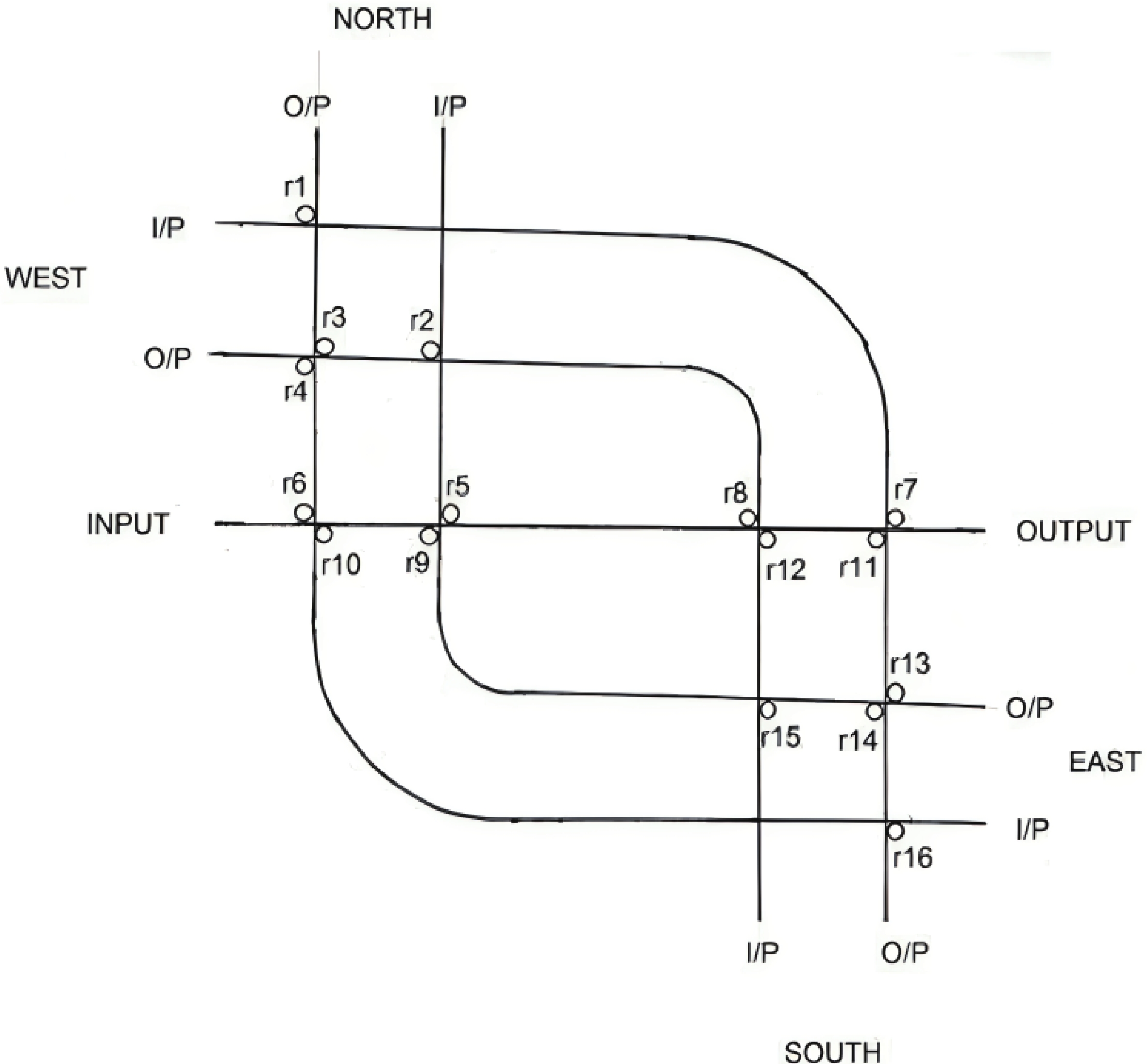
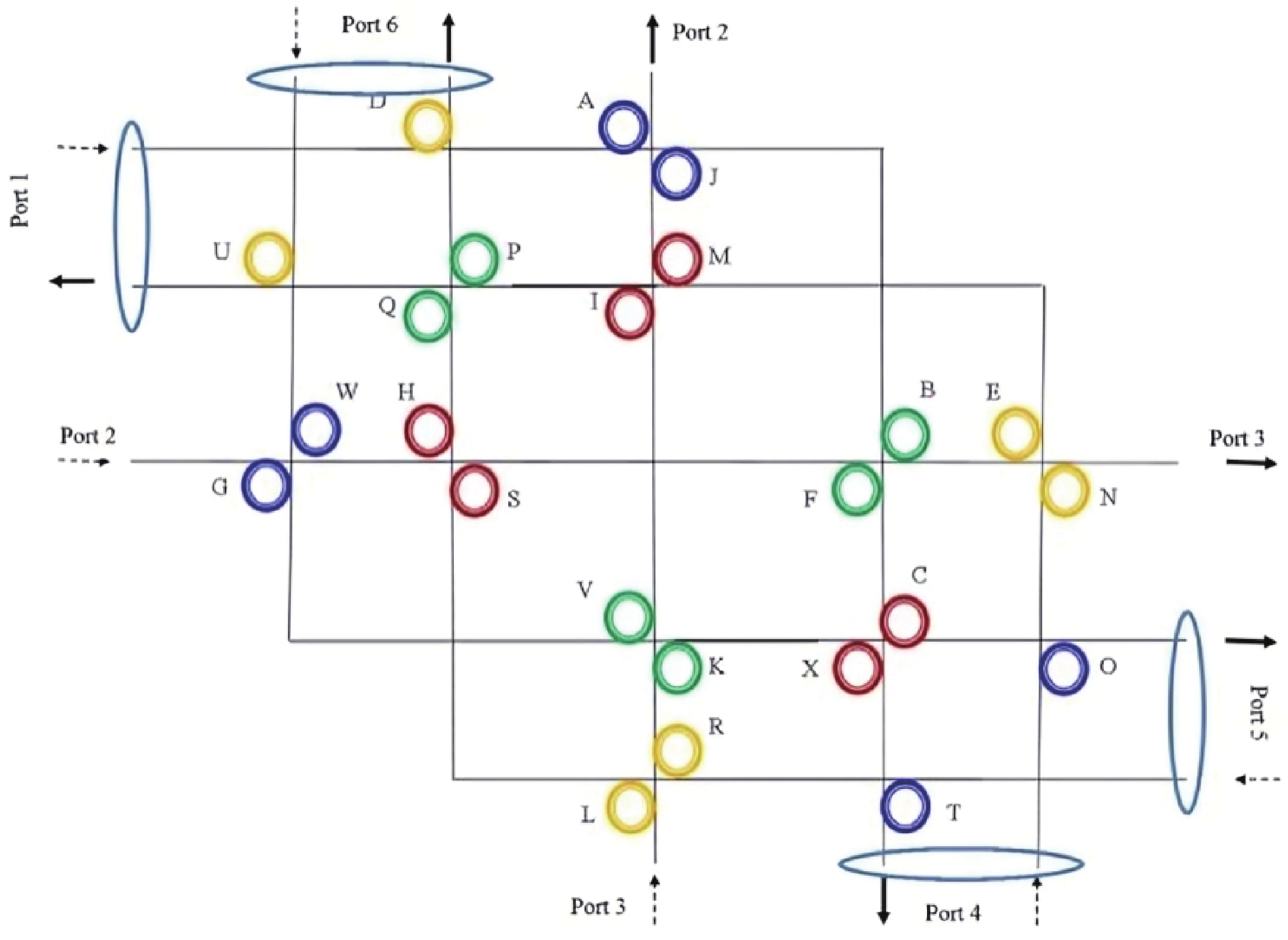
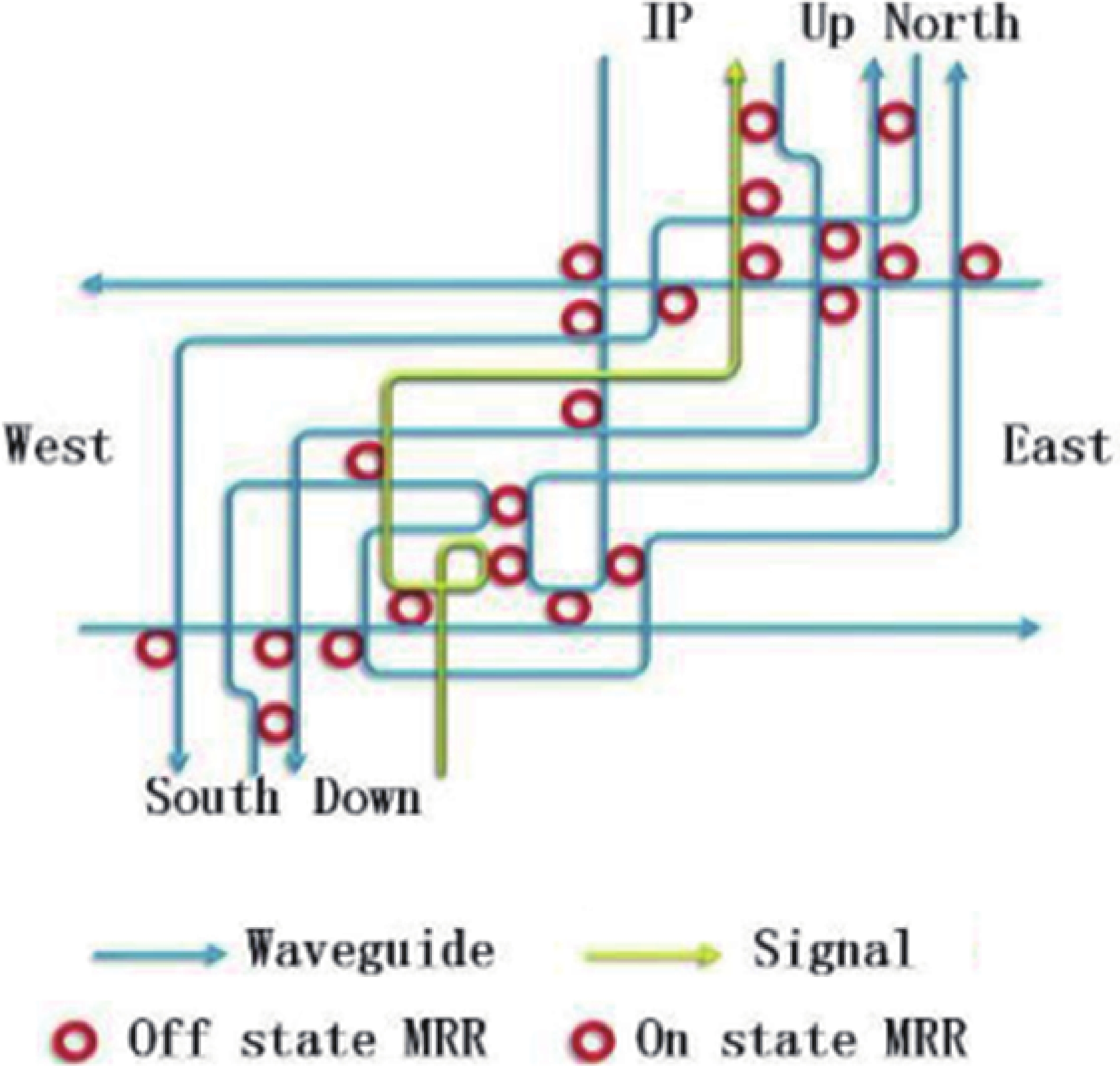
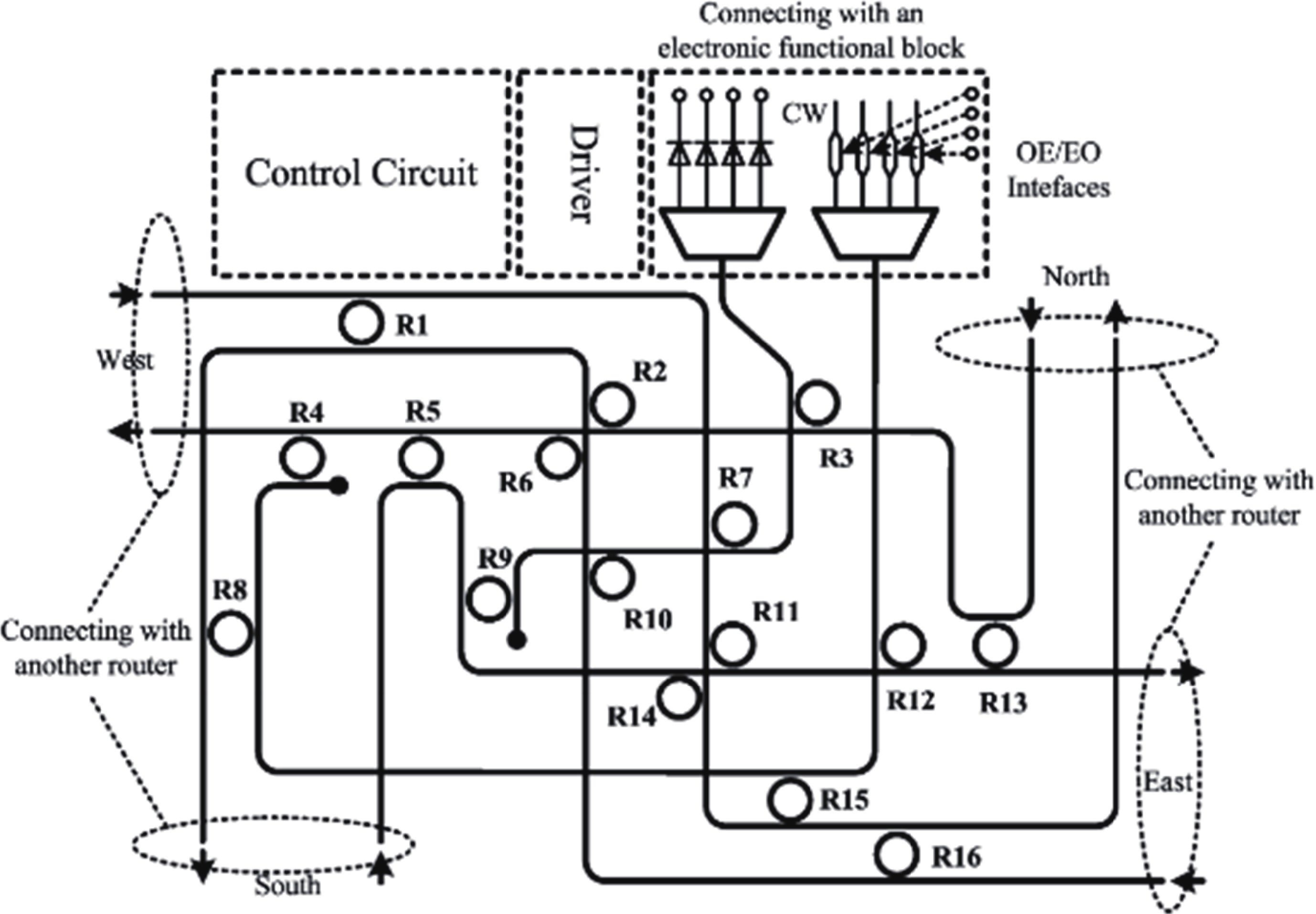
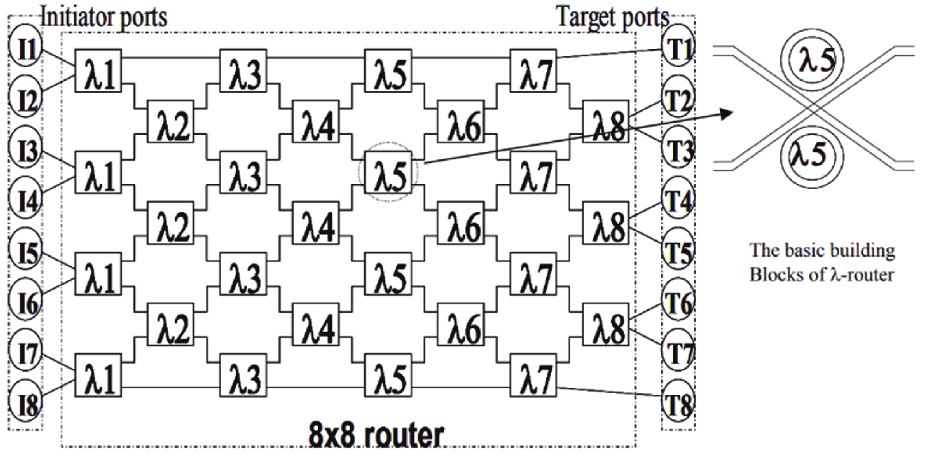
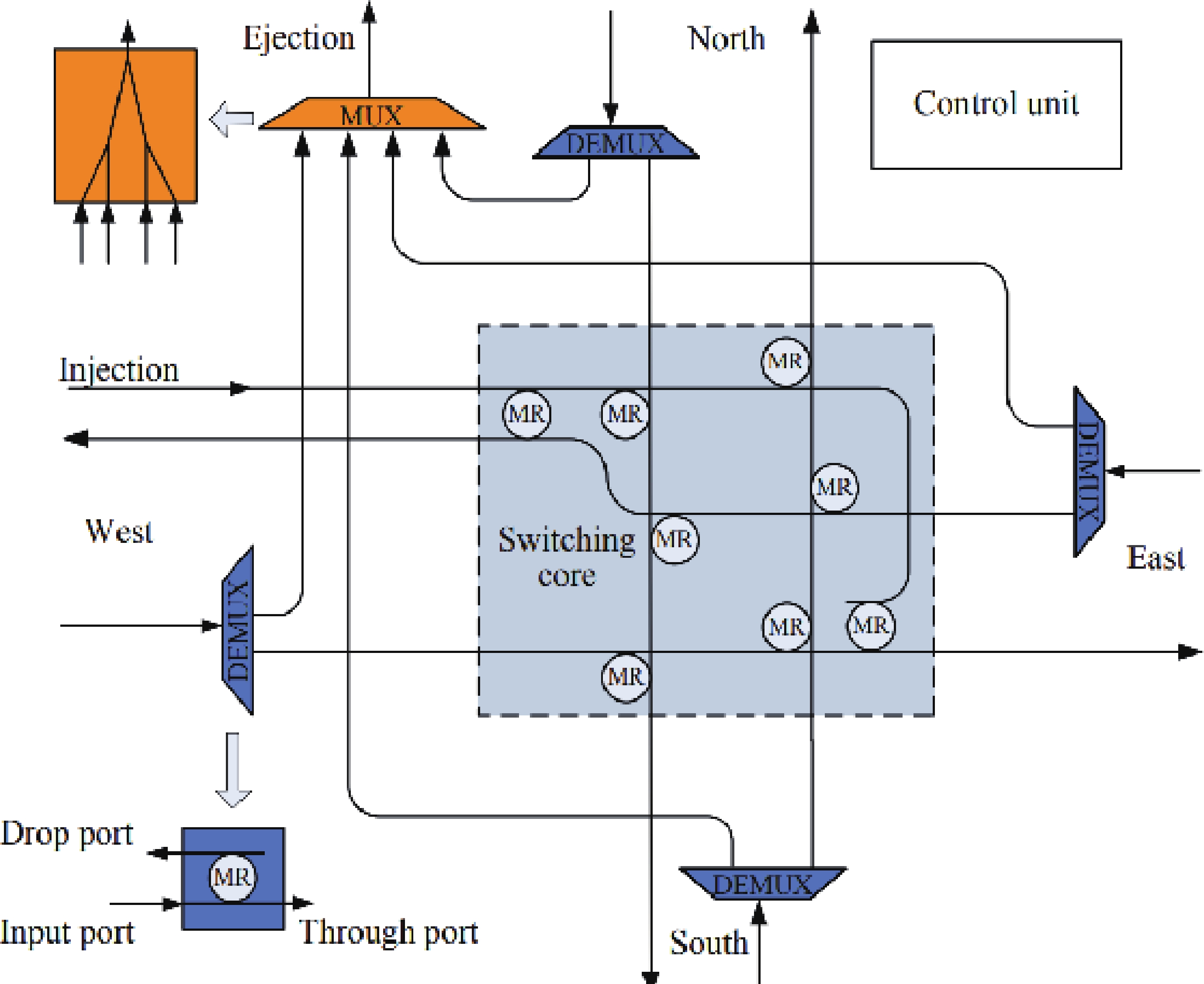
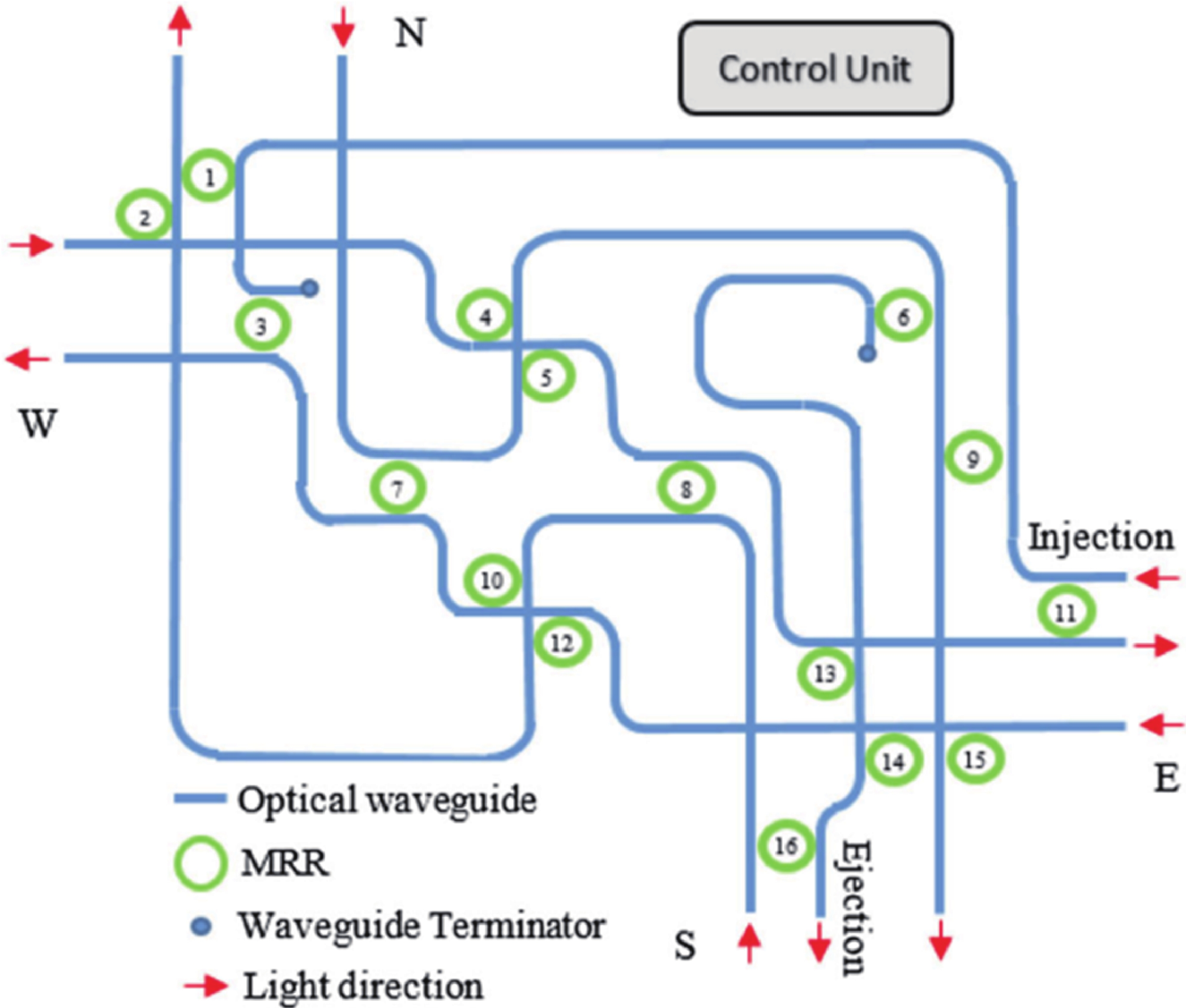
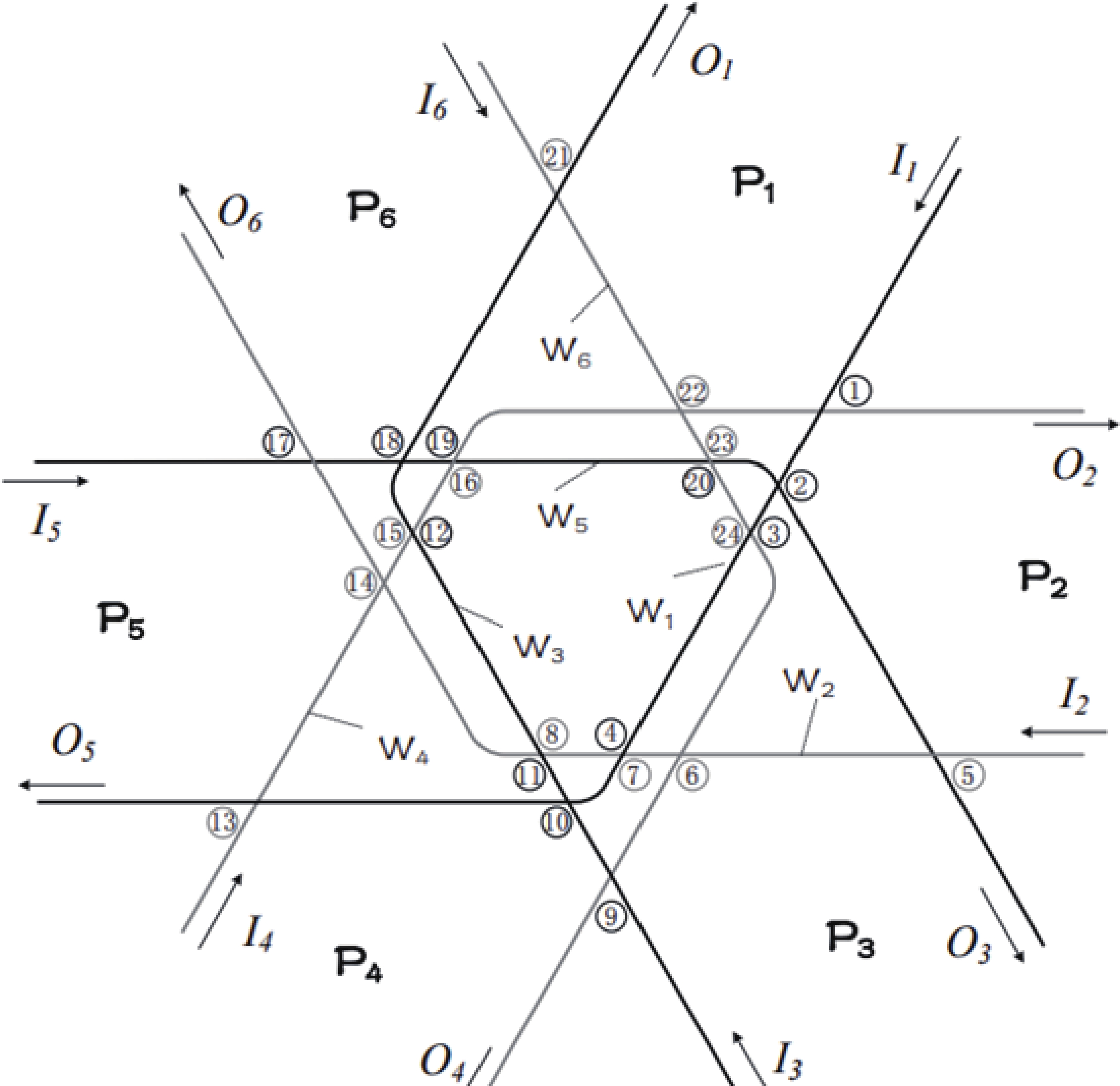
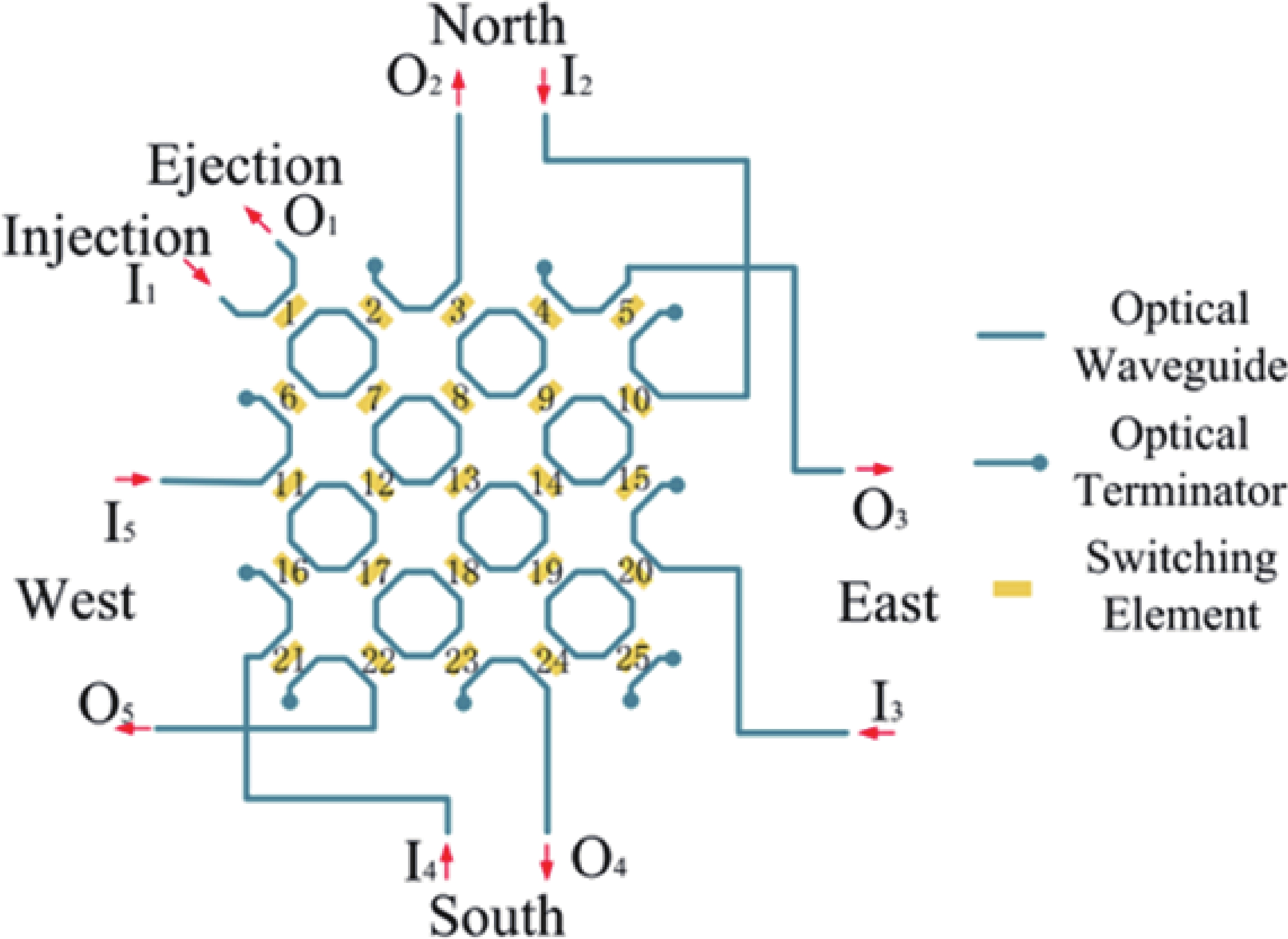
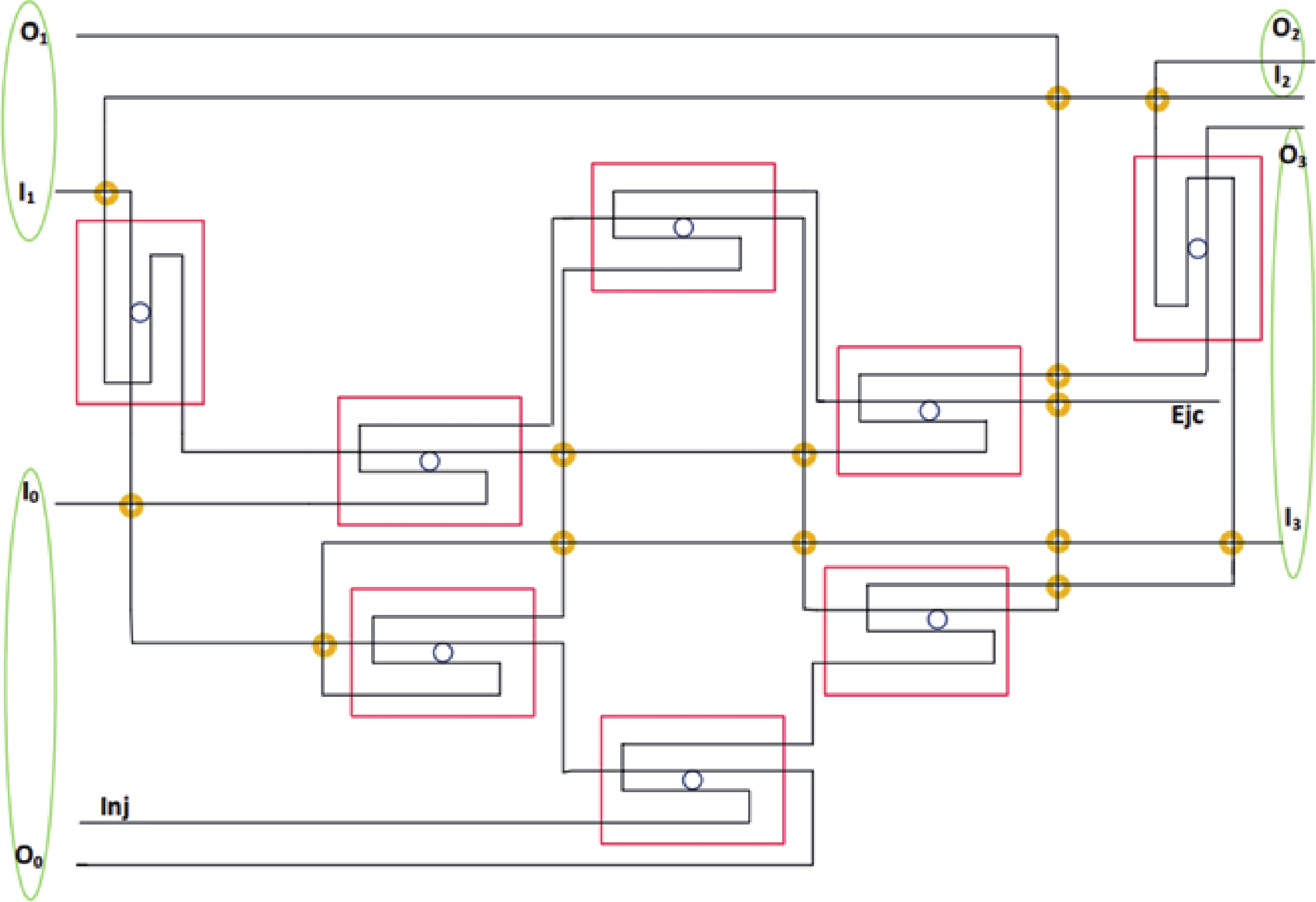
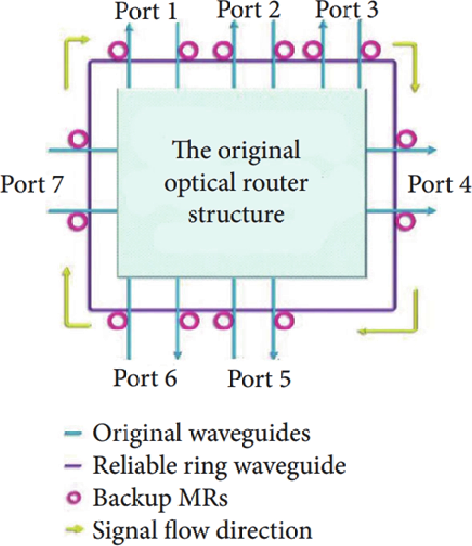
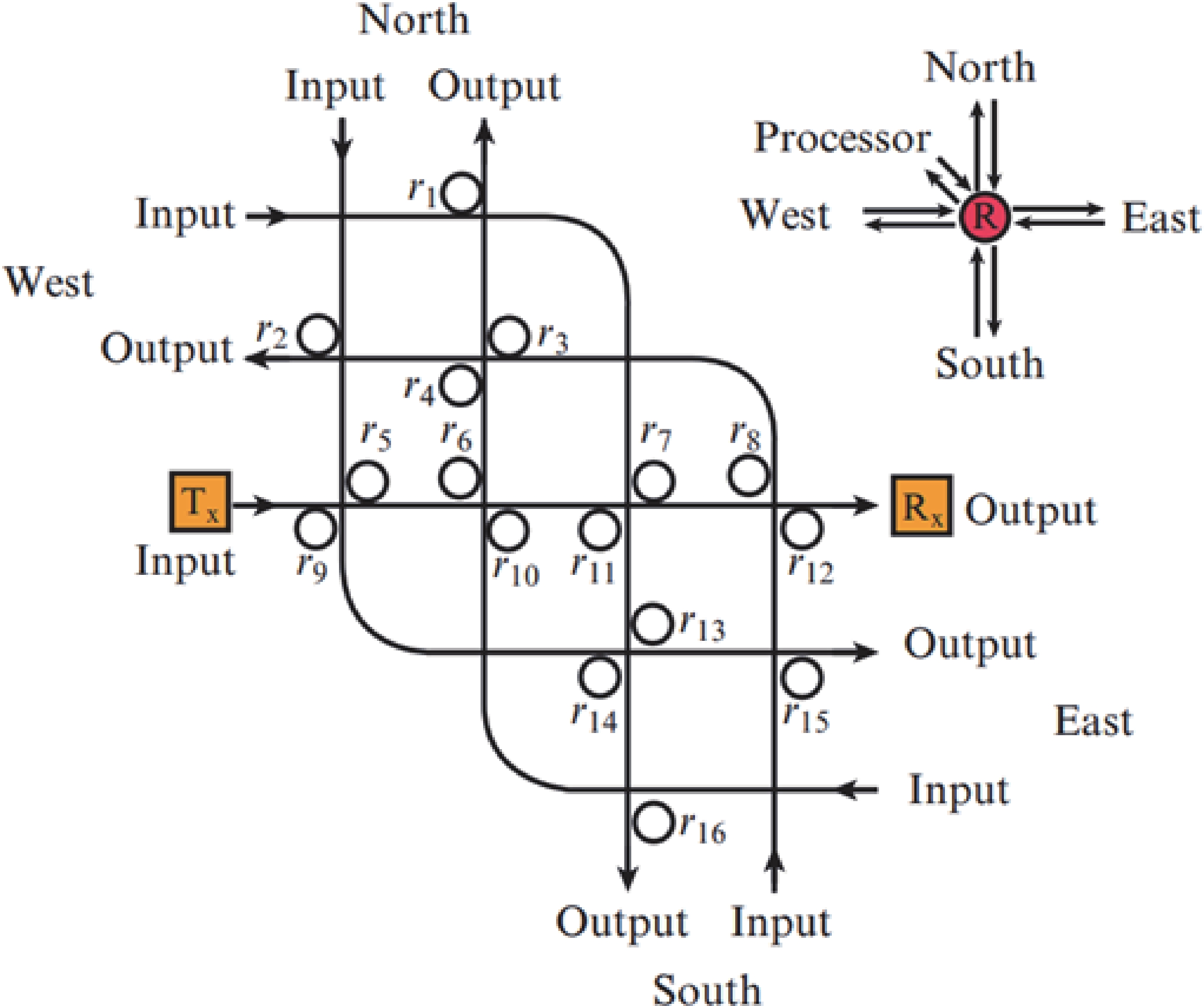
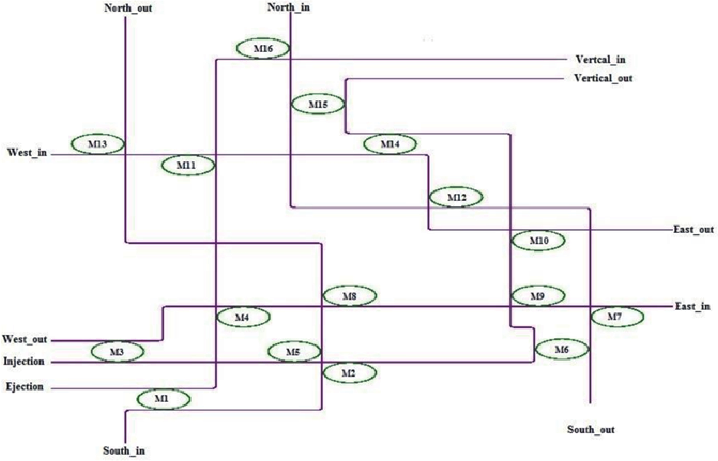
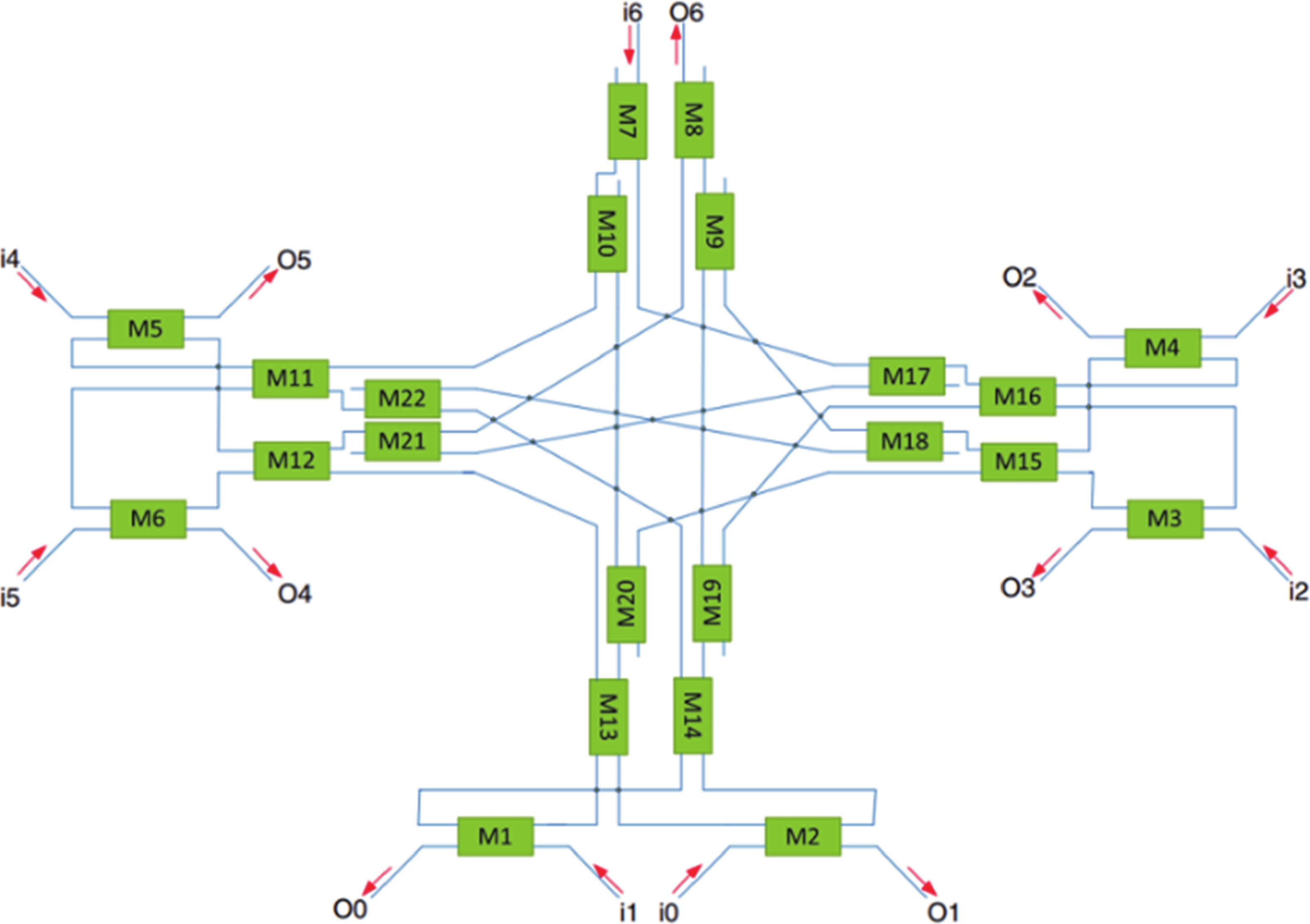
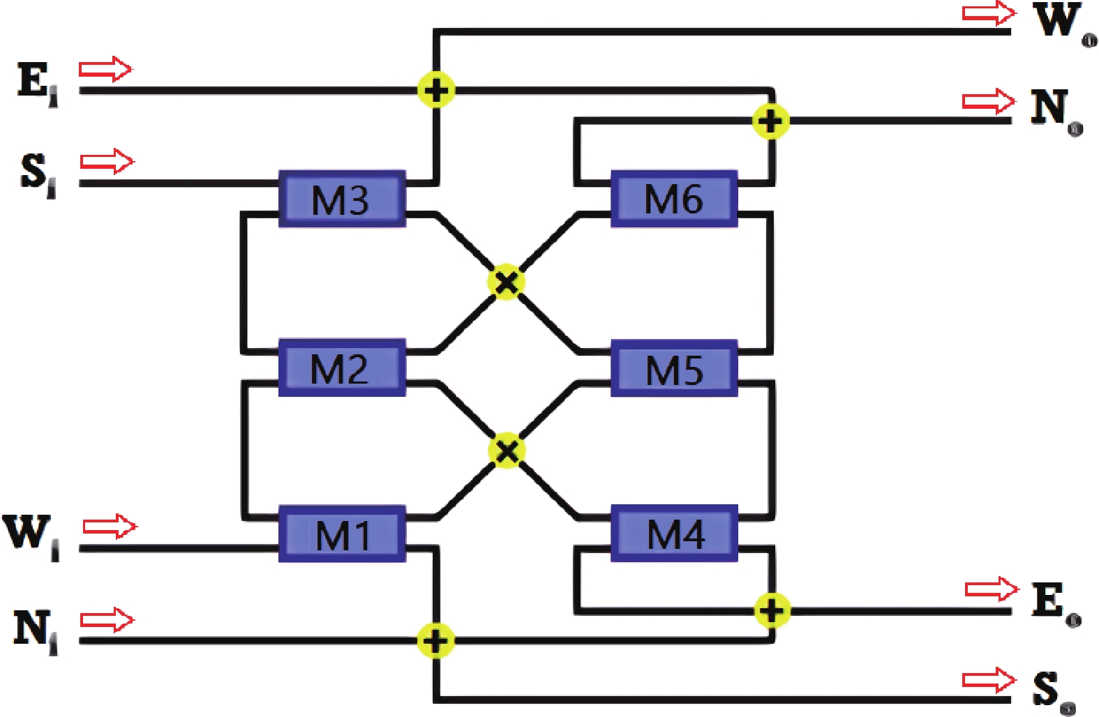
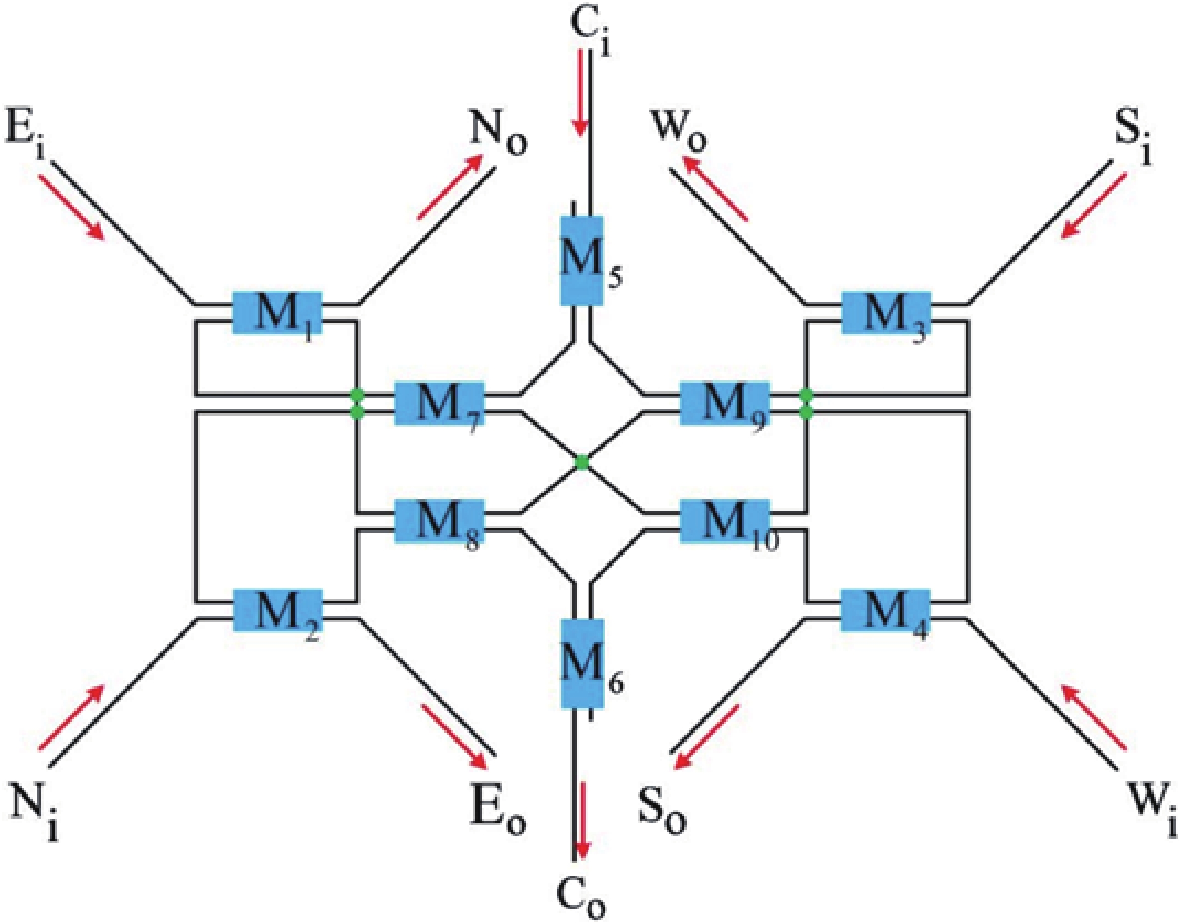
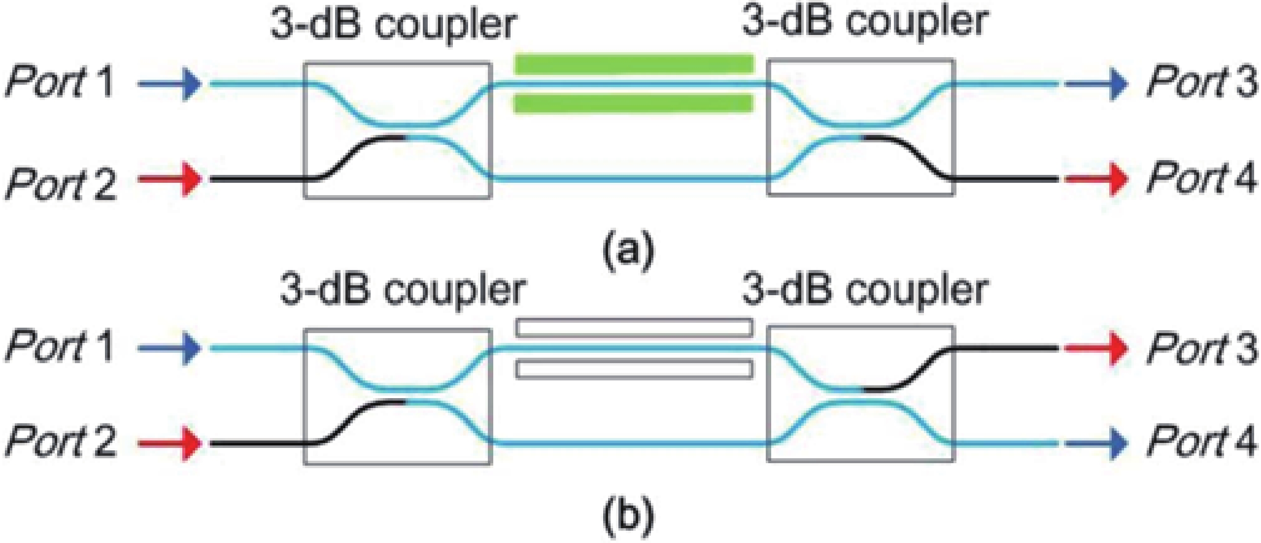
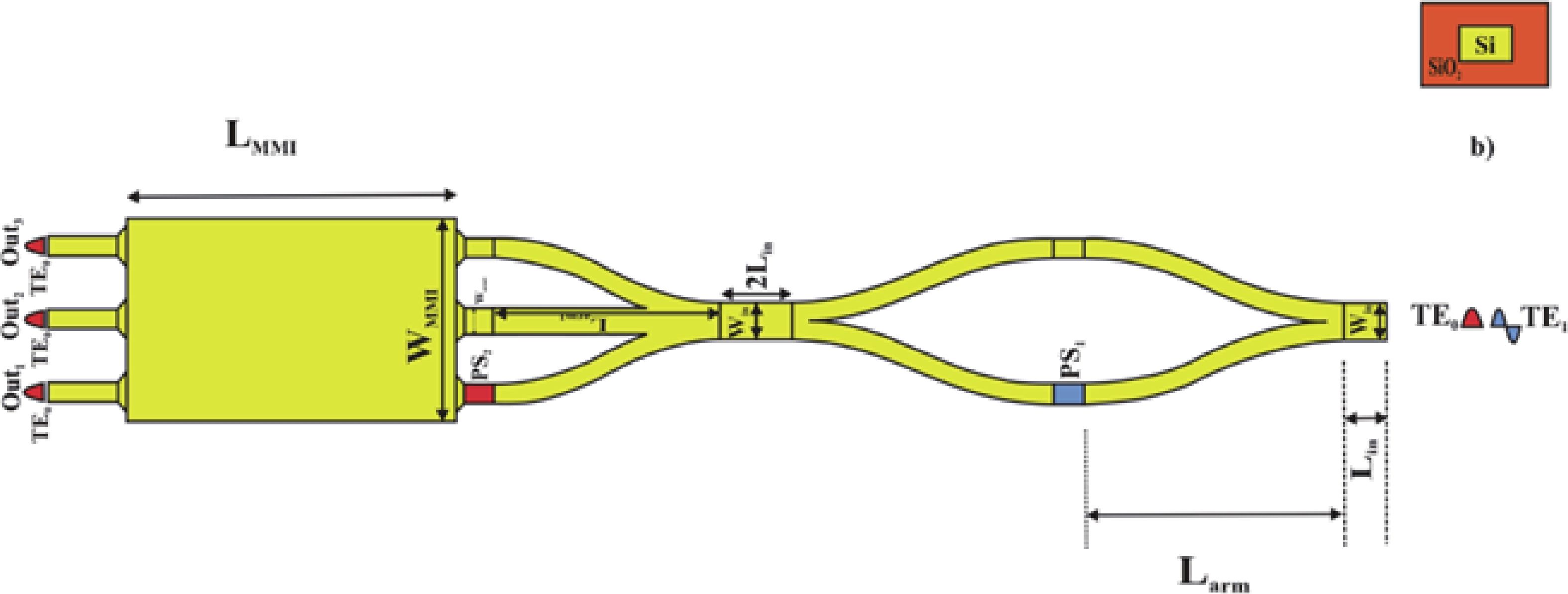
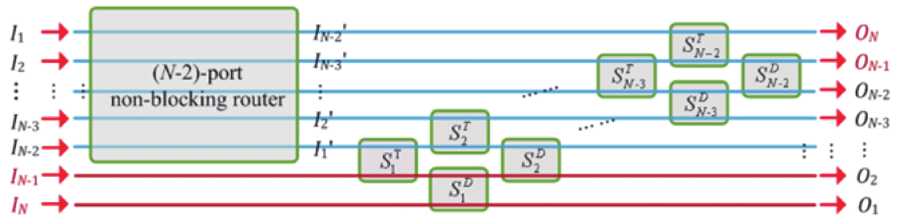
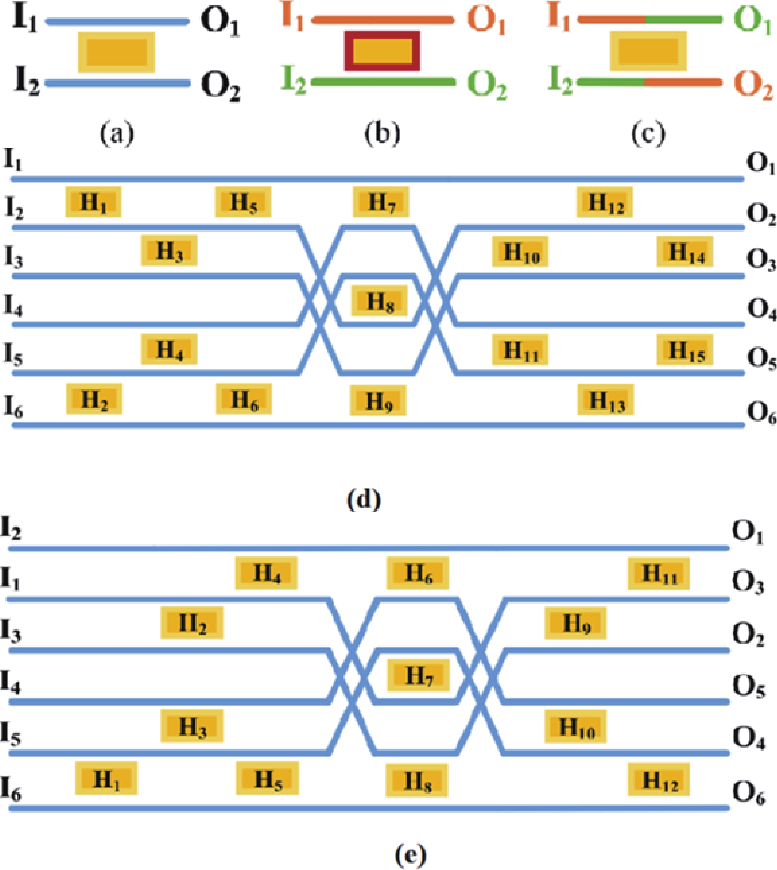
Optical network-on-chip (ONoC) systems have emerged as a promising solution to overcome limitations of traditional electronic interconnects. Efficient ONoC architectures rely on optical routers, enabling high-speed data transfer, efficient routing, and scalability. This paper presents a comprehensive survey analyzing optical router designs, specifically microring resonators (MRRs), Mach−Zehnder interferometers (MZIs), and hybrid architectures. Selected comparison criteria, chosen for their critical importance, significantly impact router functionality and performance. By emphasizing these criteria, valuable insights into the strengths and limitations of different designs are gained, facilitating informed decisions and advancements in optical networking. While other factors contribute to performance and efficiency, the chosen criteria consistently address fundamental elements, enabling meaningful evaluation. This work serves as a valuable resource for beginners, providing a solid foundation in understanding ONoC and optical routers. It also offers an in-depth survey for experts, laying the groundwork for further exploration. Additionally, the importance of considering design constraints and requirements when selecting an optimal router design is highlighted. Continued research and innovation will enable the development of efficient optical router solutions that meet the evolving needs of modern computing systems. This survey underscores the significance of ongoing advancements in the field and their potential impact on future technologies.
J. Semicond.
2025, 46(3): 032101 doi: 10.1088/1674-4926/24090035
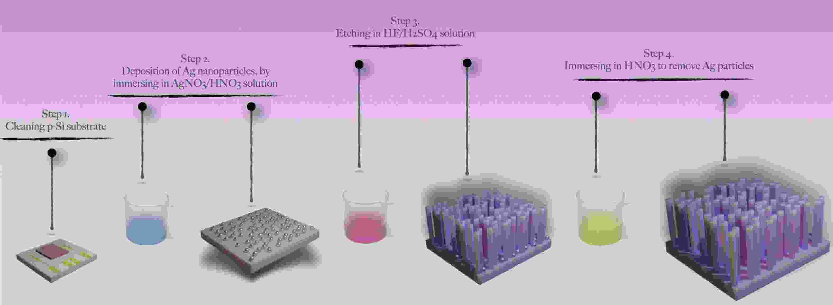
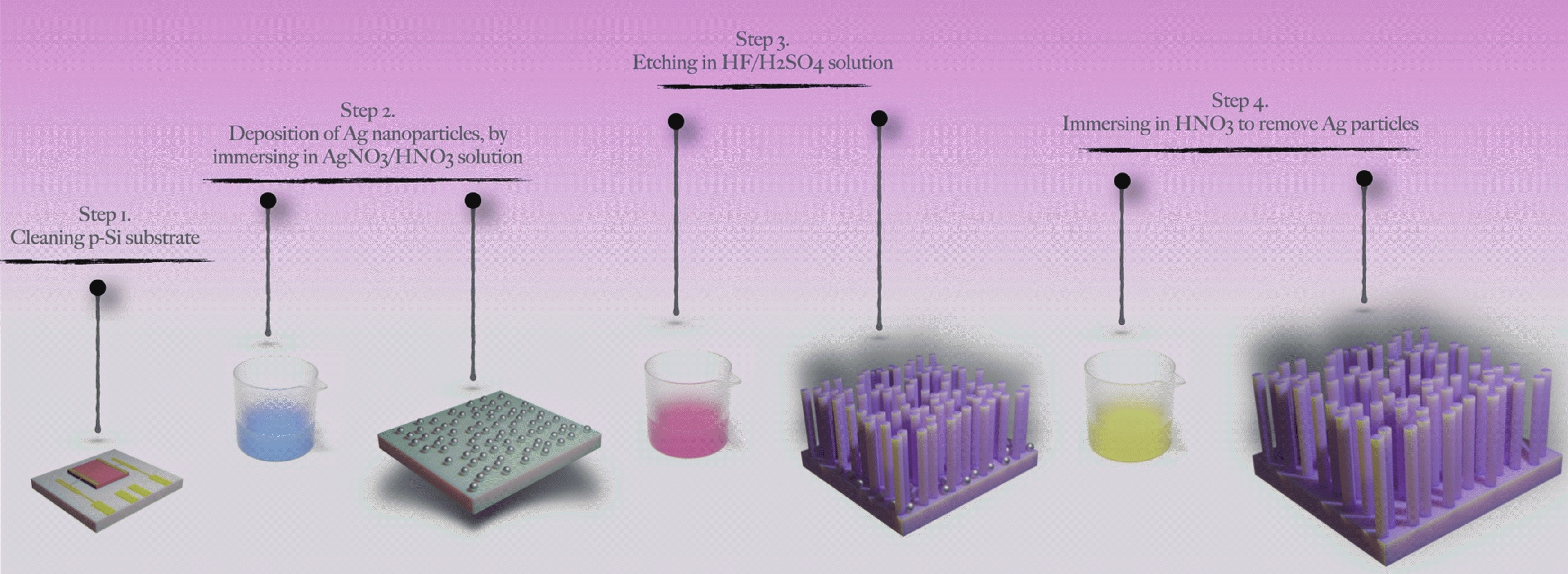
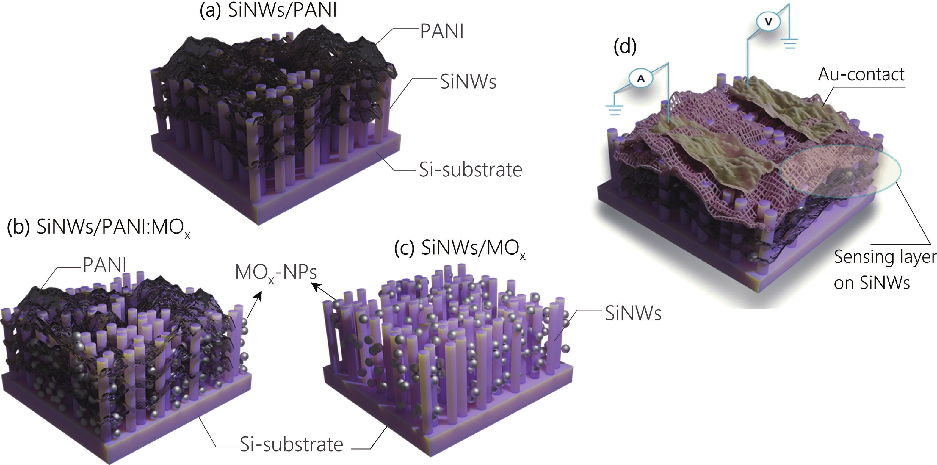
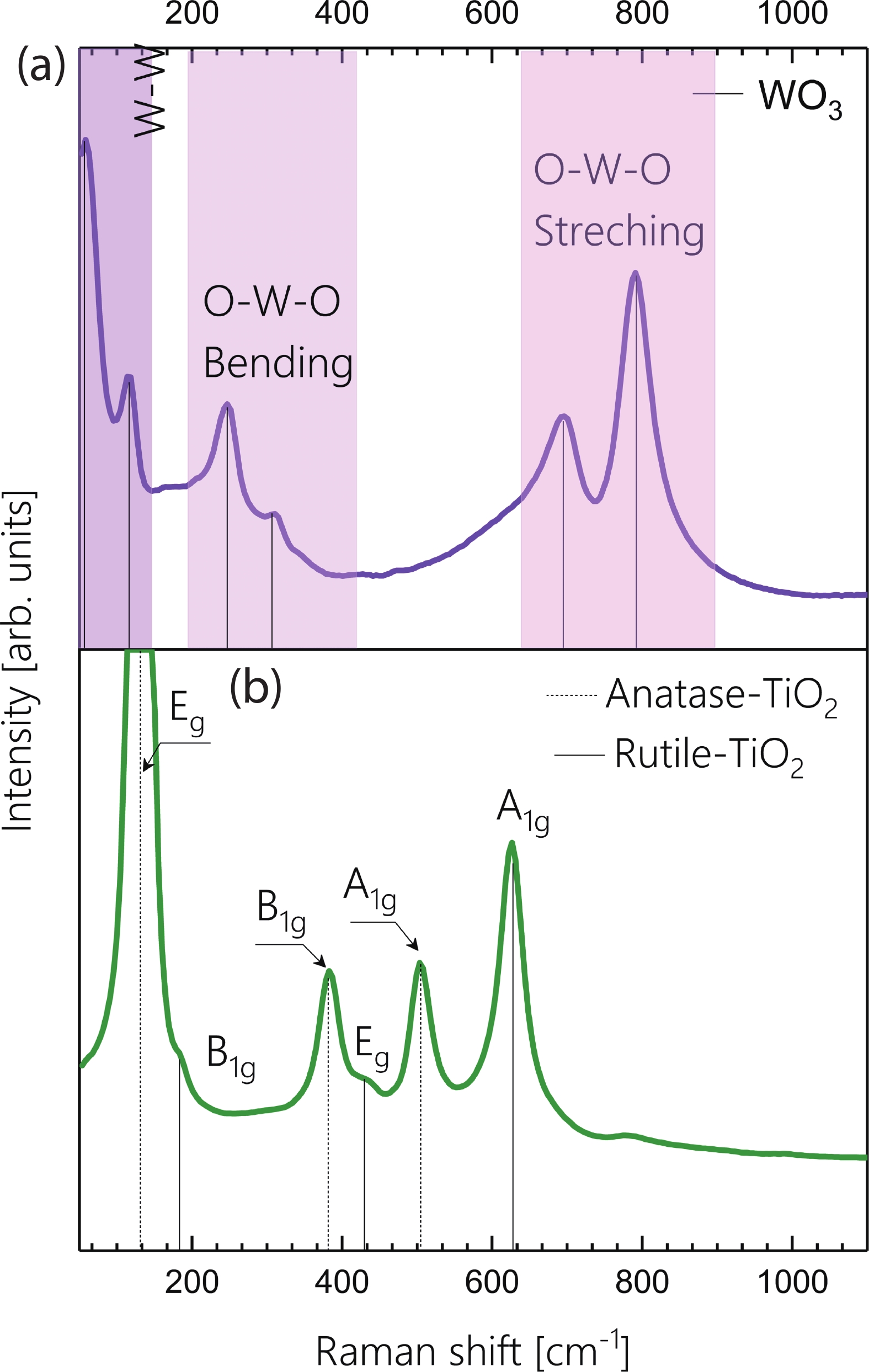
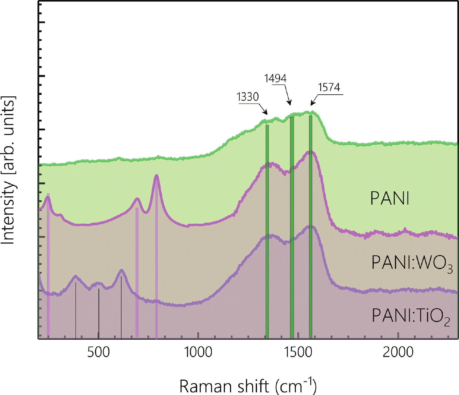
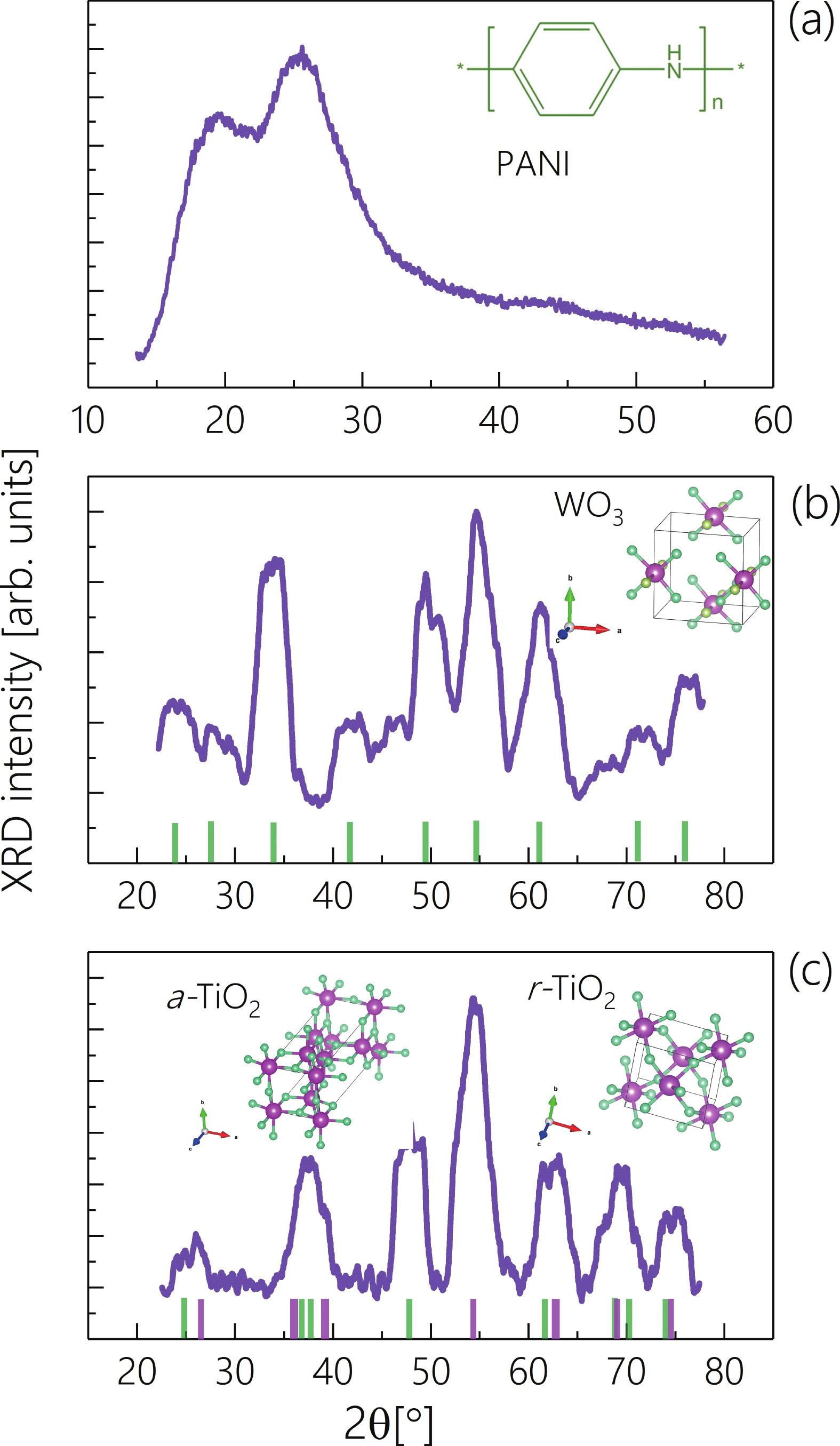
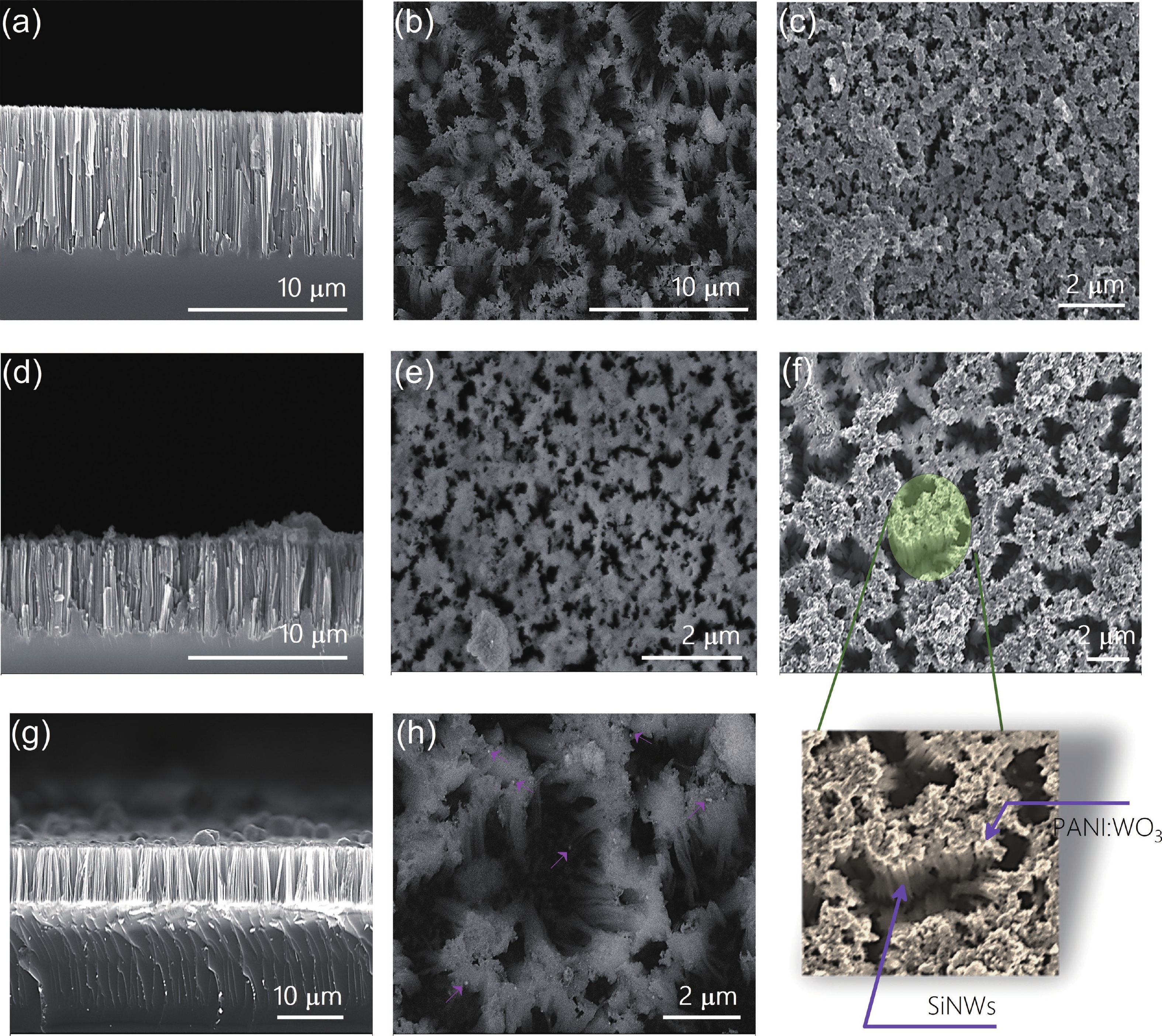
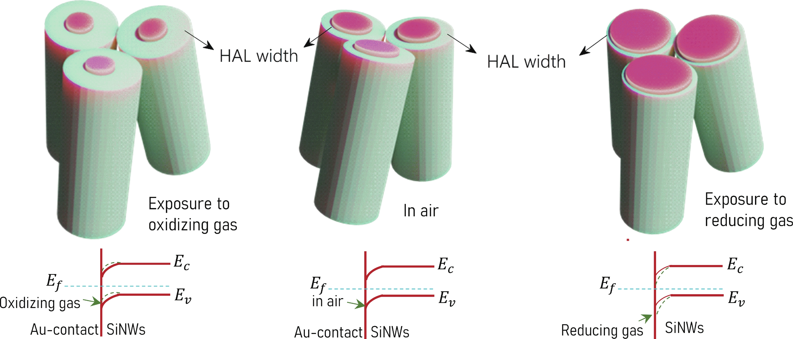
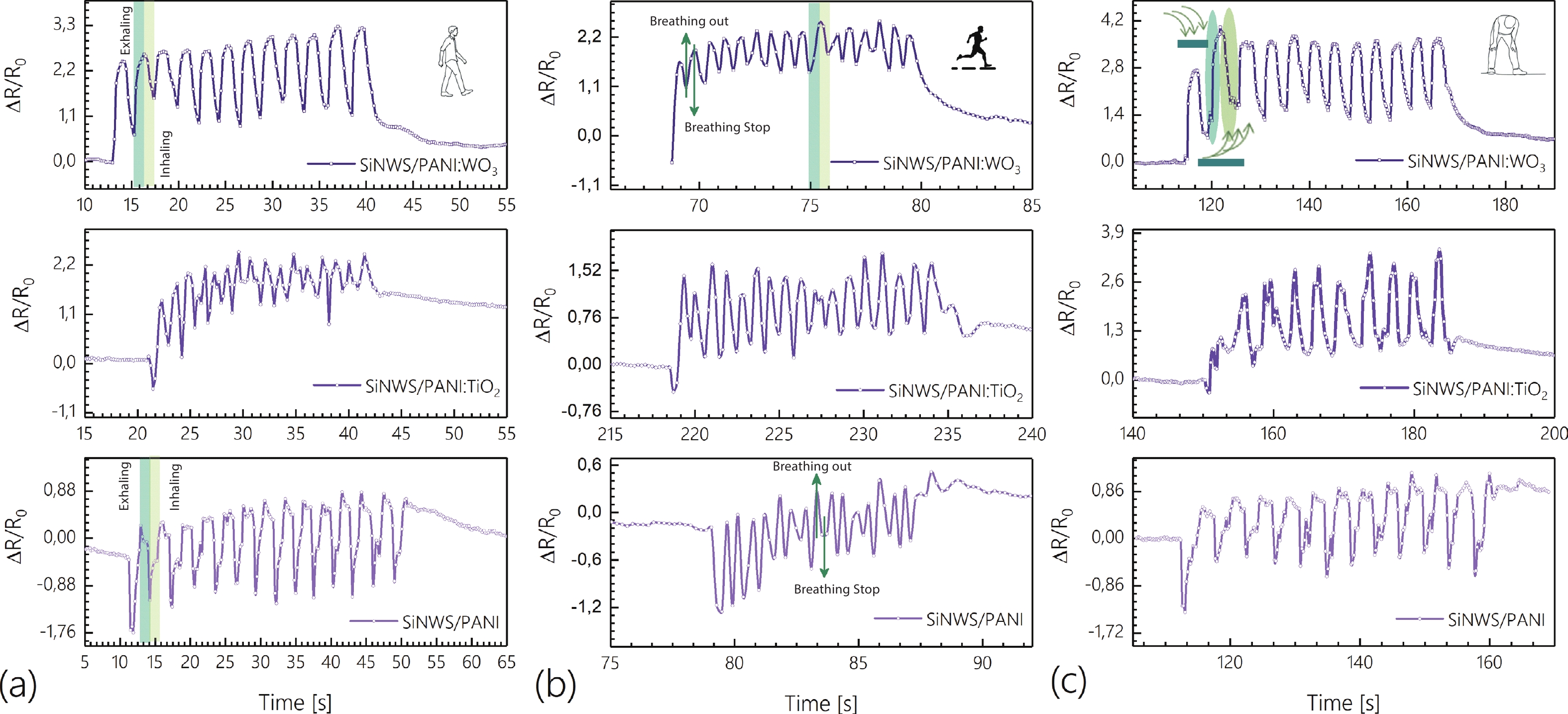
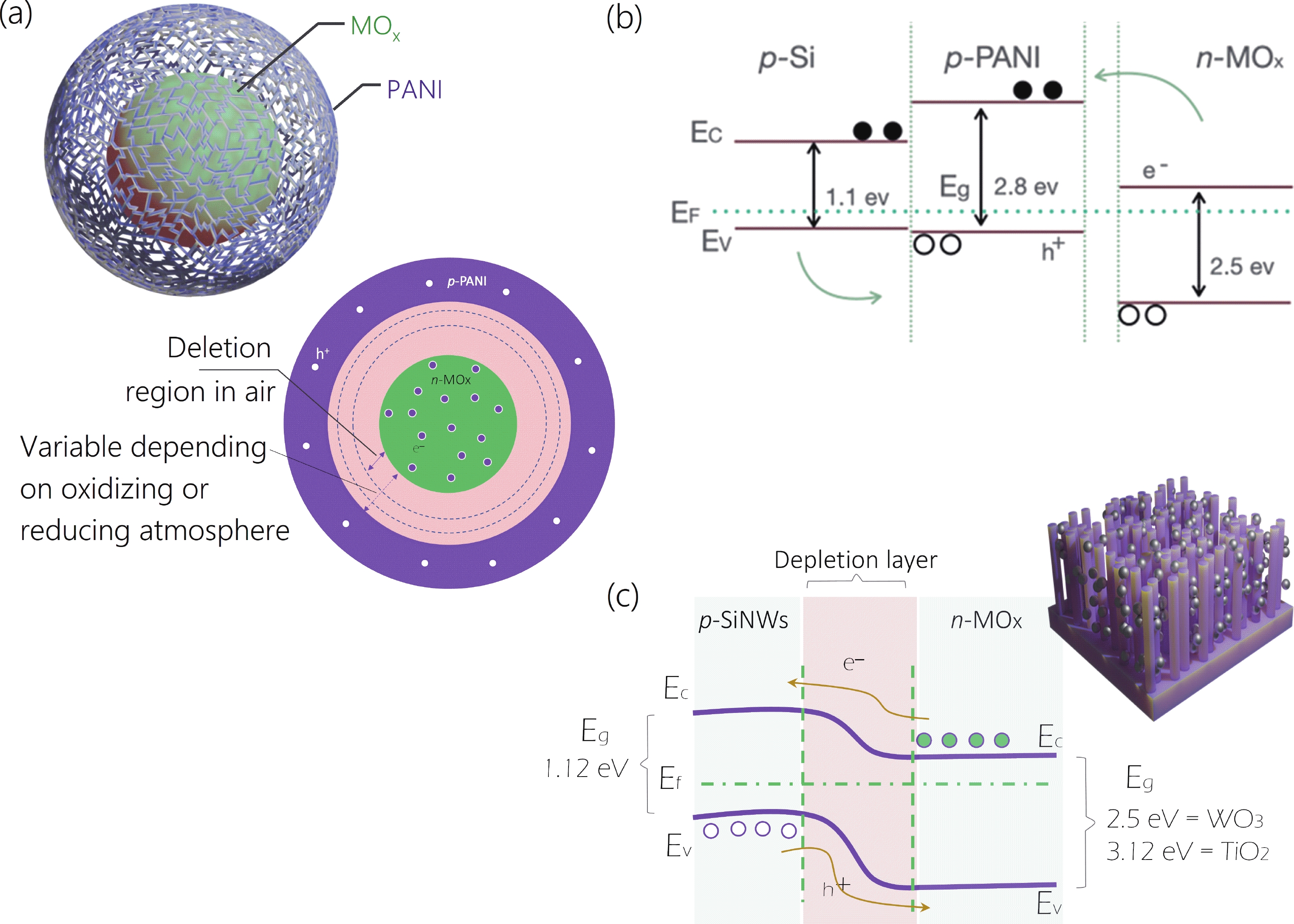
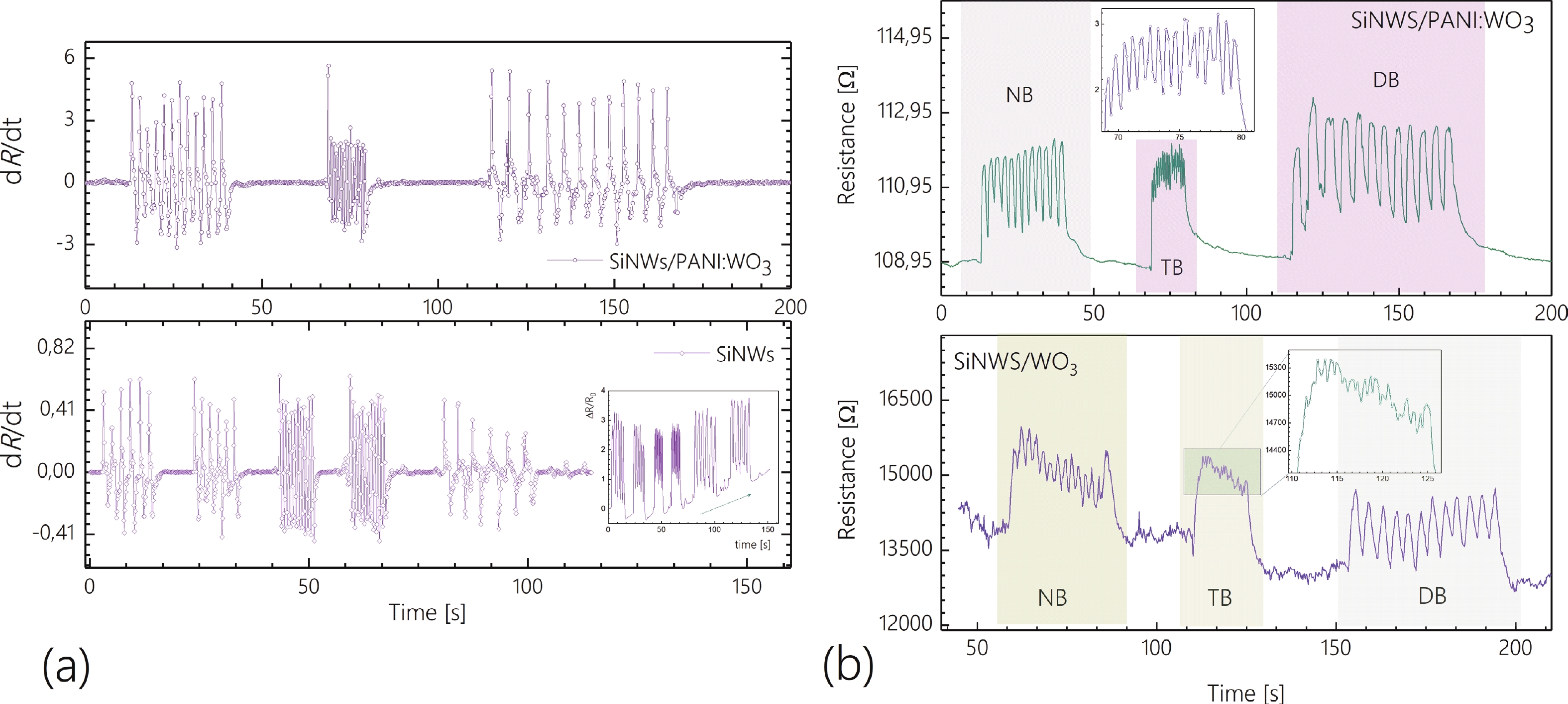
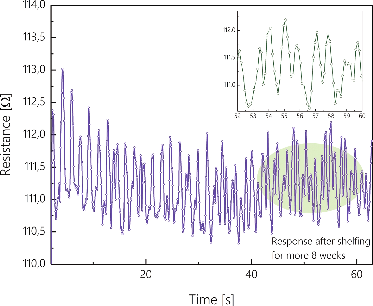
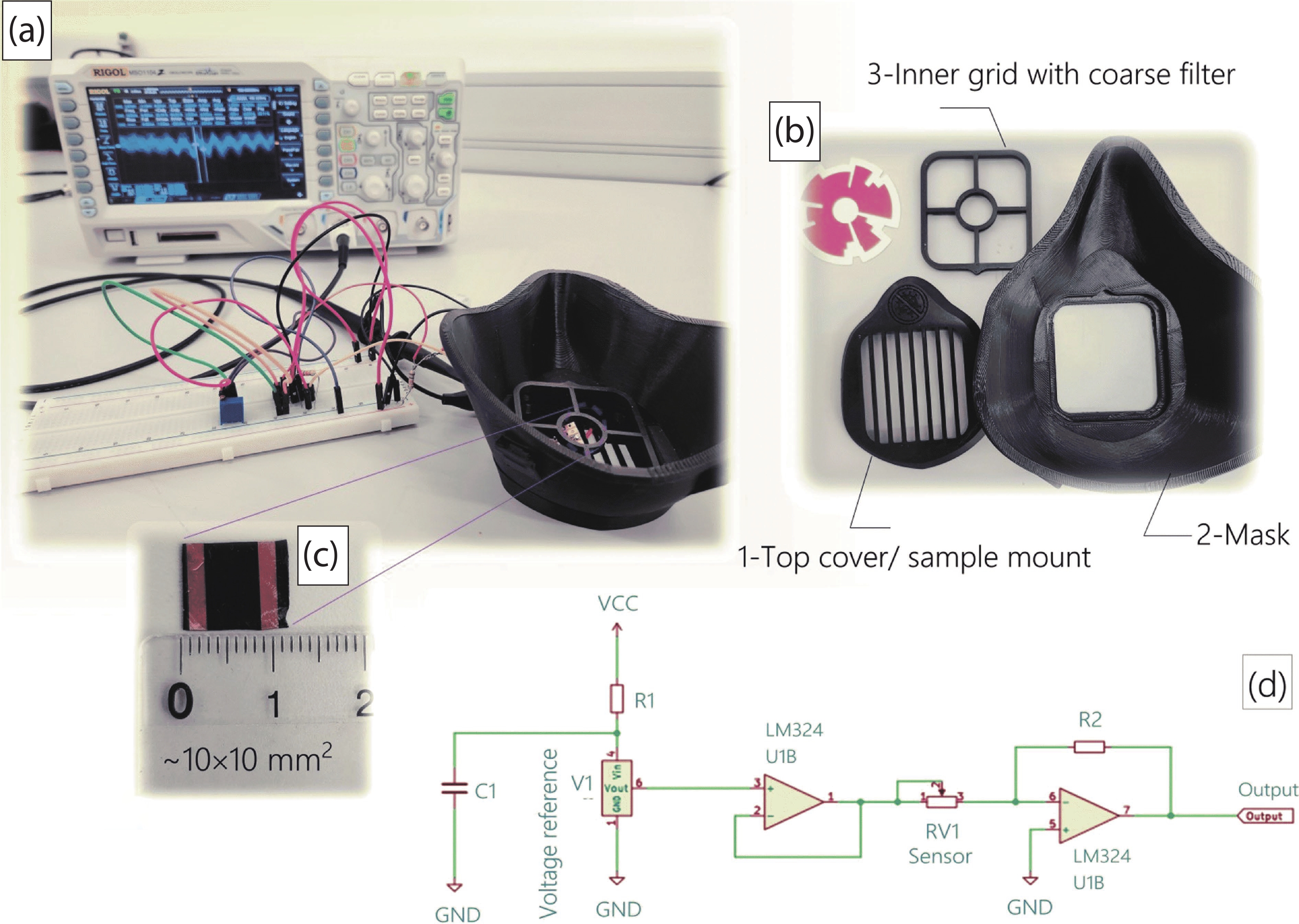
In this study, we investigate an innovative hybrid structure of silicon nanowires (SiNWs) coated with polyaniline (PANI):metal oxide (MOx) nanoparticles, i.e., WO3 and TiO2, for respiratory sensing. To date, few attempts have been made to utilize such hybrid structures for that application. The SiNWs were fabricated using metal-assisted chemical etching (MACE), whereas PANI:MOx was deposited using chemical oxidative polymerization. The structures were characterized using Raman spectroscopy, X-ray diffraction, and scanning electron microscopy. The sensing characteristics revealed that the hybrid sensor exhibited a considerably better response than pure SiNWs:MOx and SiNWs:PANI. Such an enhancement in sensitivity is attributed to the formation of a p−n heterojunction between PANI and MOx, the wider conduction channel provided by PANI, increased porosity in SiNWs/PANI:WO3 hybrid structures, which creates active sites, increased oxygen vacancies, and the large surface area compared to that available in pure MOx nanoparticles. Furthermore, less baseline drift and increased sensor stability were established for the SiNWs structure coated with PANI:WO3, as compared to PANI:TiO2.
J. Semicond.
2025, 46(3): 032201 doi: 10.1088/1674-4926/24100022

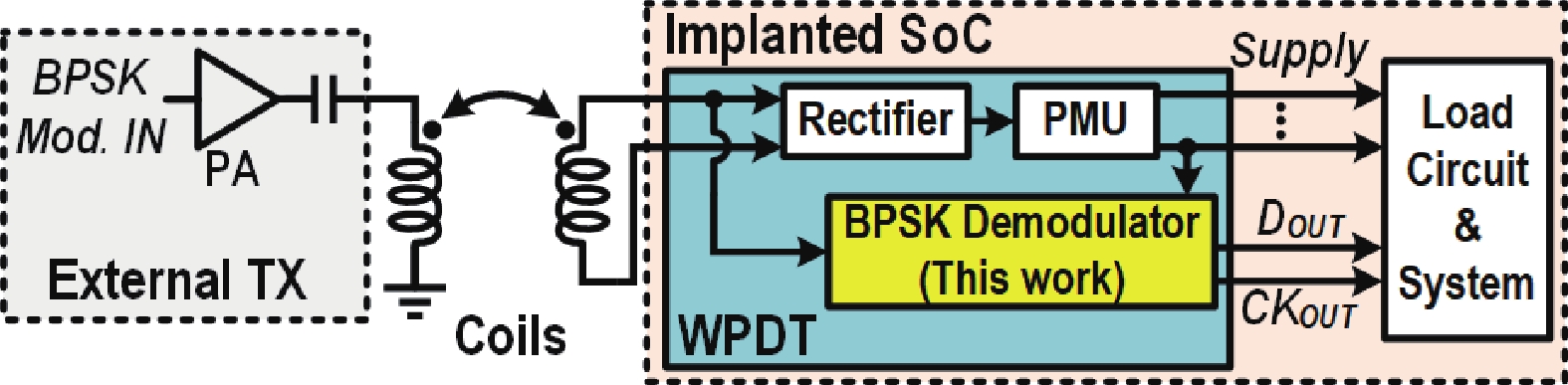
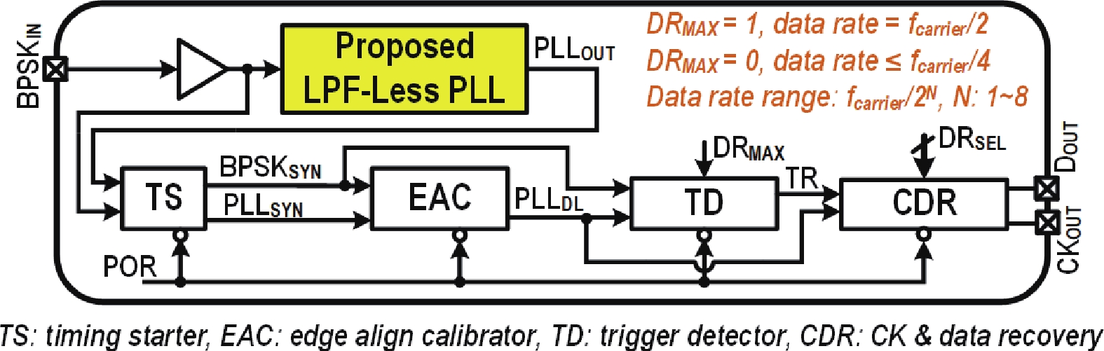
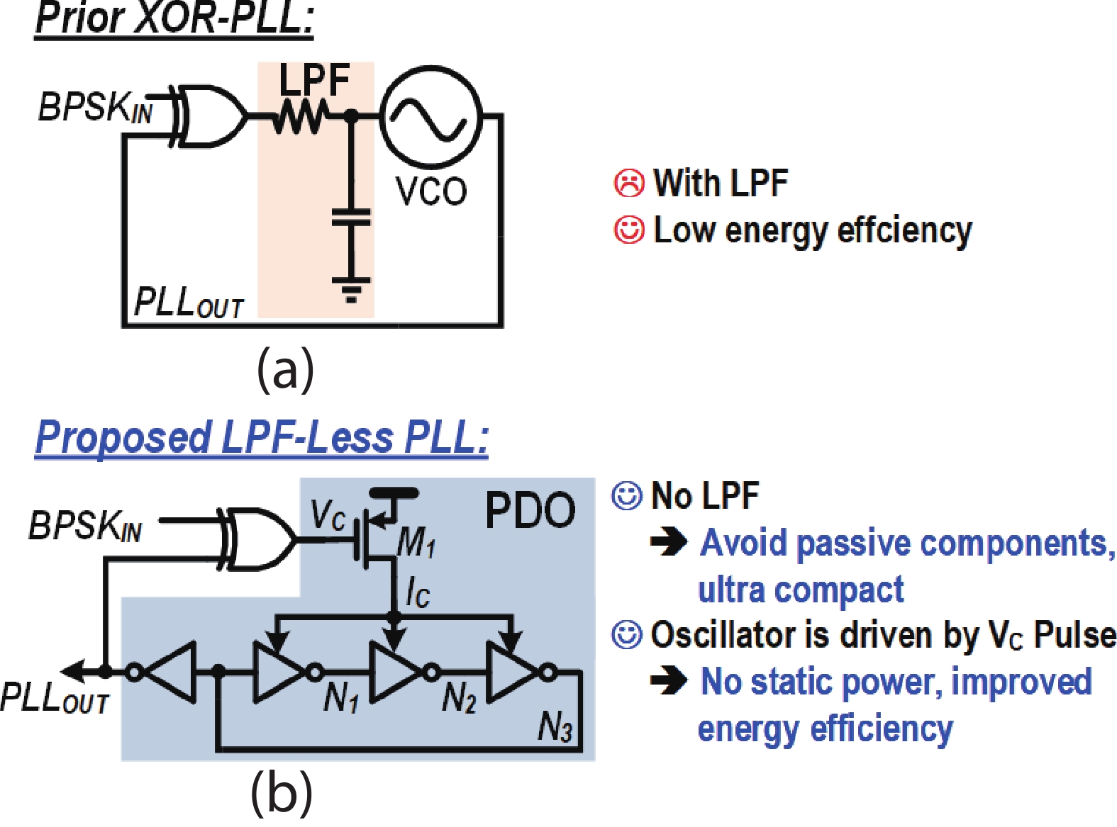
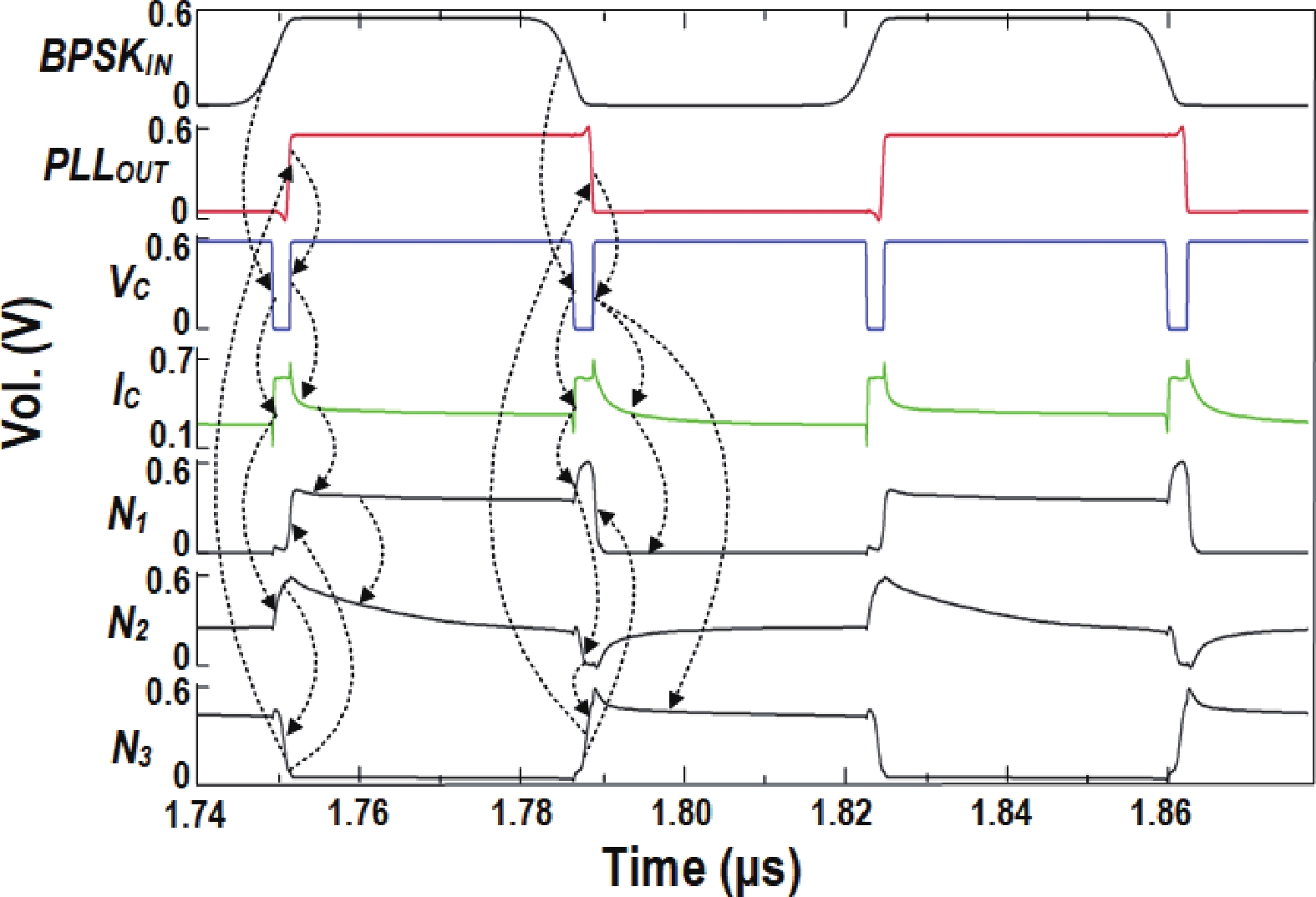
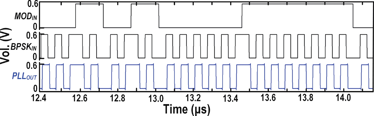
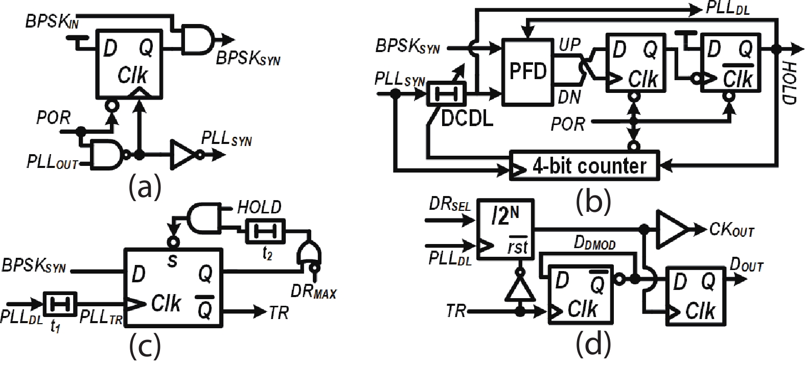
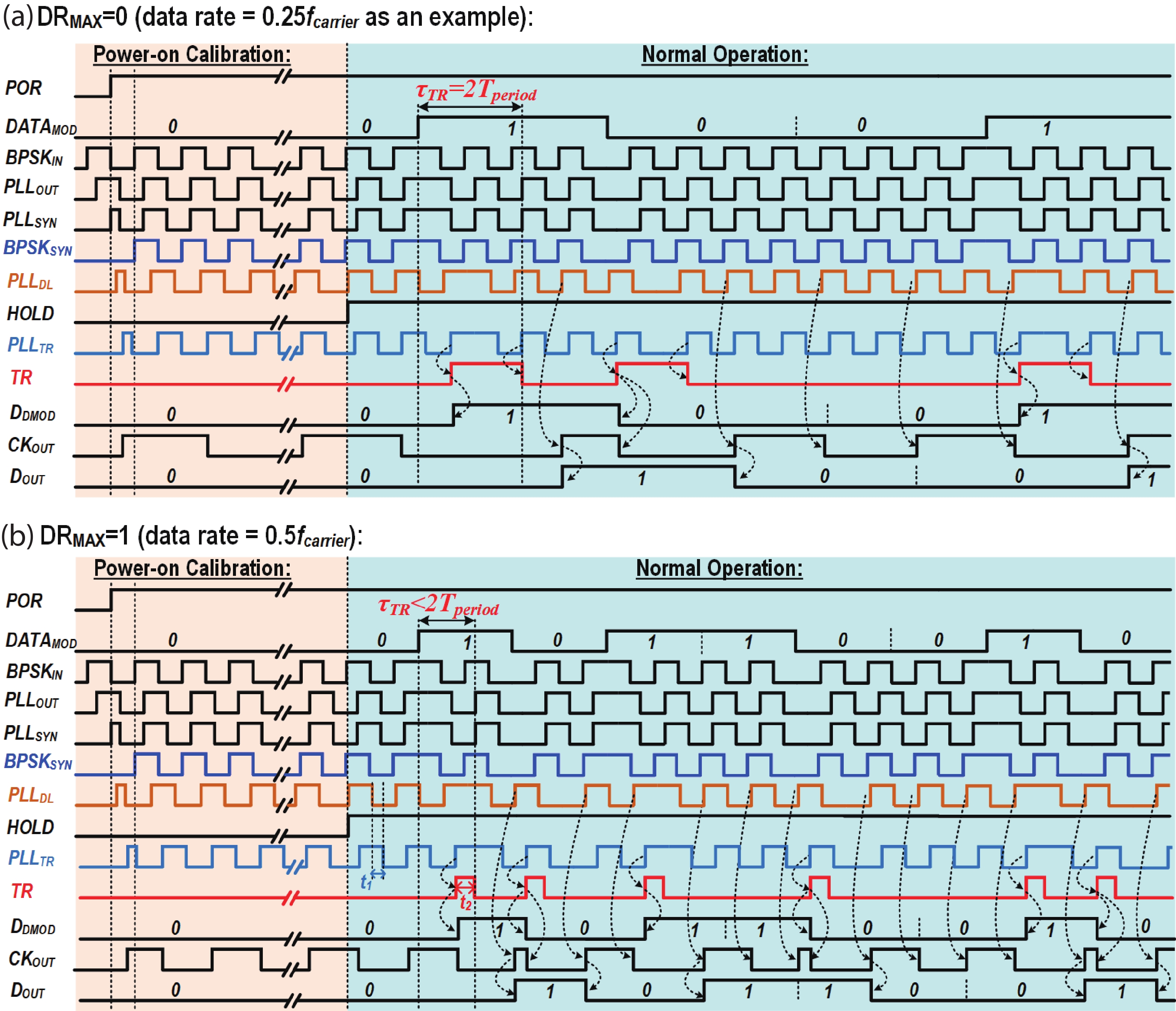
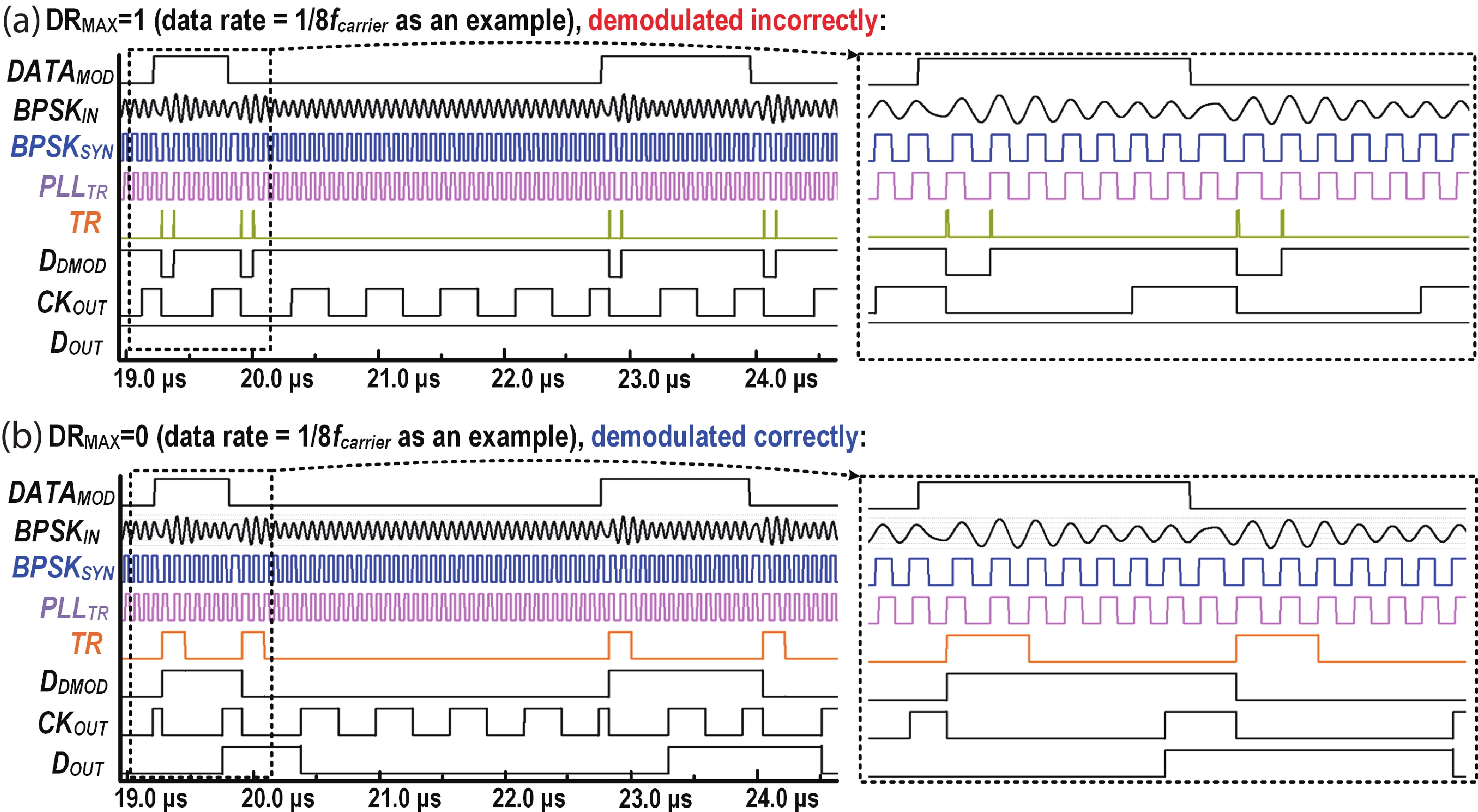
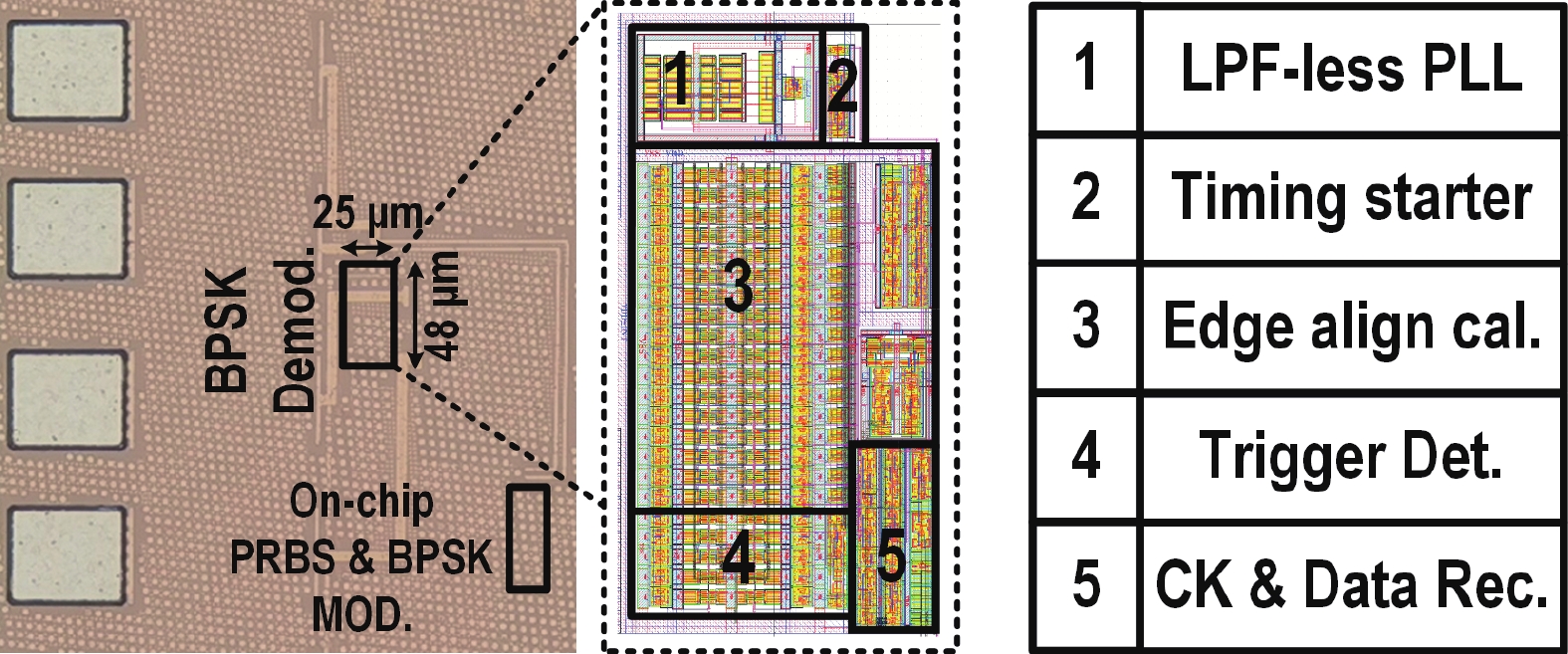
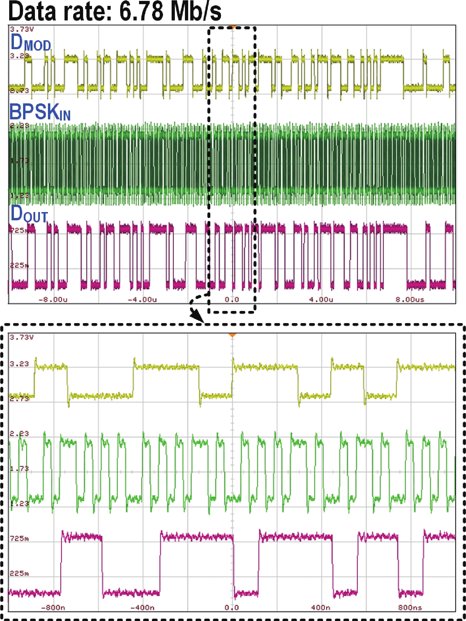
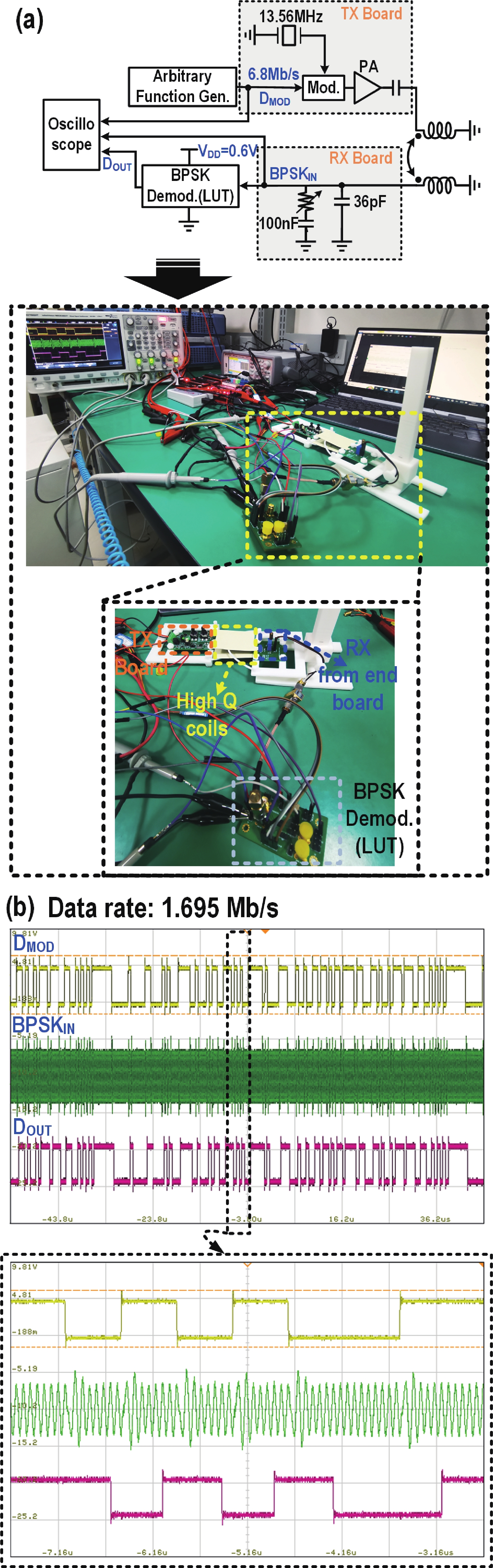
This paper presents a compact ultra-low-power phase-locked loop (PLL) based binary phase-shift keying (BPSK) demodulator. The loop-filter-less (LPF-less) PLL is proposed to make phase of PLL output carrier signal track the phase of BPSK signal in real time. Thus, the maximum date rate can be significantly extended to the half of the carrier frequency (fcarrier) with a very compact size compared to prior PLL-based BPSK demodulators. Furthermore, eliminating all the static power in our LPF-less PLL, the energy efficiency is obviously improved. Fabricated in a 40-nm CMOS process, our prototype occupies 0.0012-mm2 core active area, and achieves the maximum data rate of 6.78 Mb/s (fcarrier/2) at fcarrier of 13.56 MHz. The power consumption and energy efficiency is 4.47 μW and 0.66 pJ/bit at 6.78-Mb/s data rate, respectively.
J. Semicond.
2025, 46(3): 032301 doi: 10.1088/1674-4926/24090037
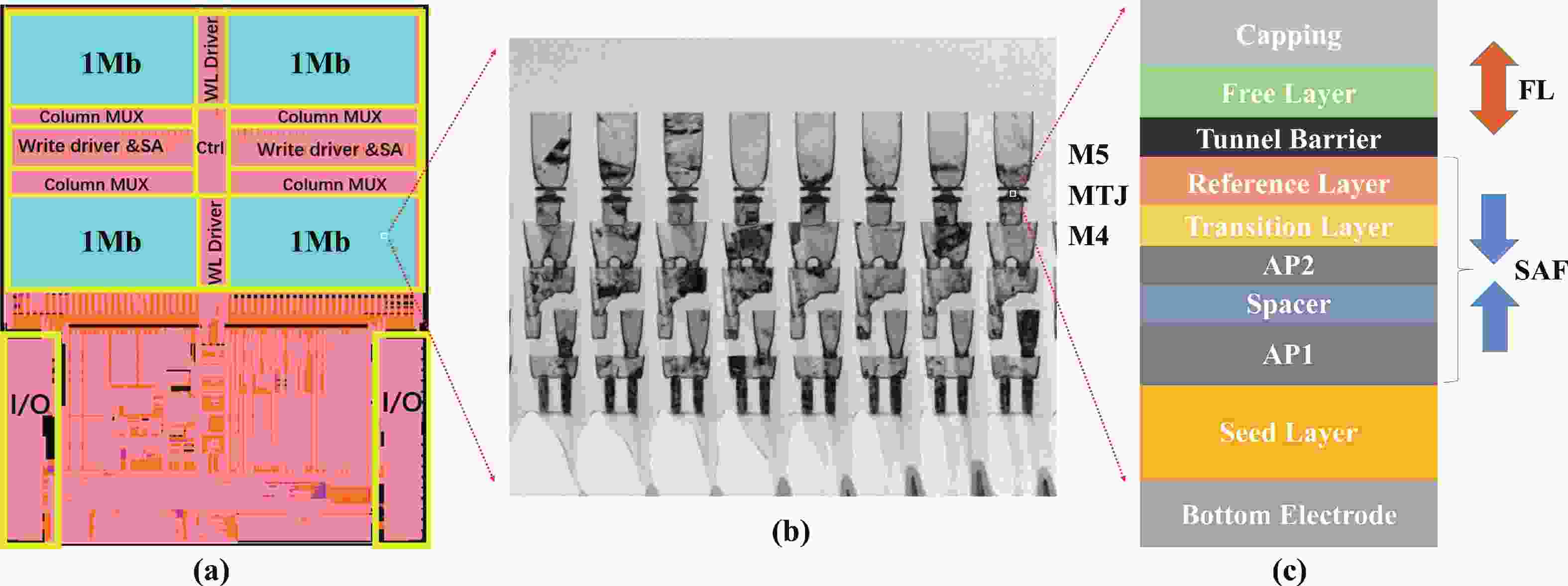
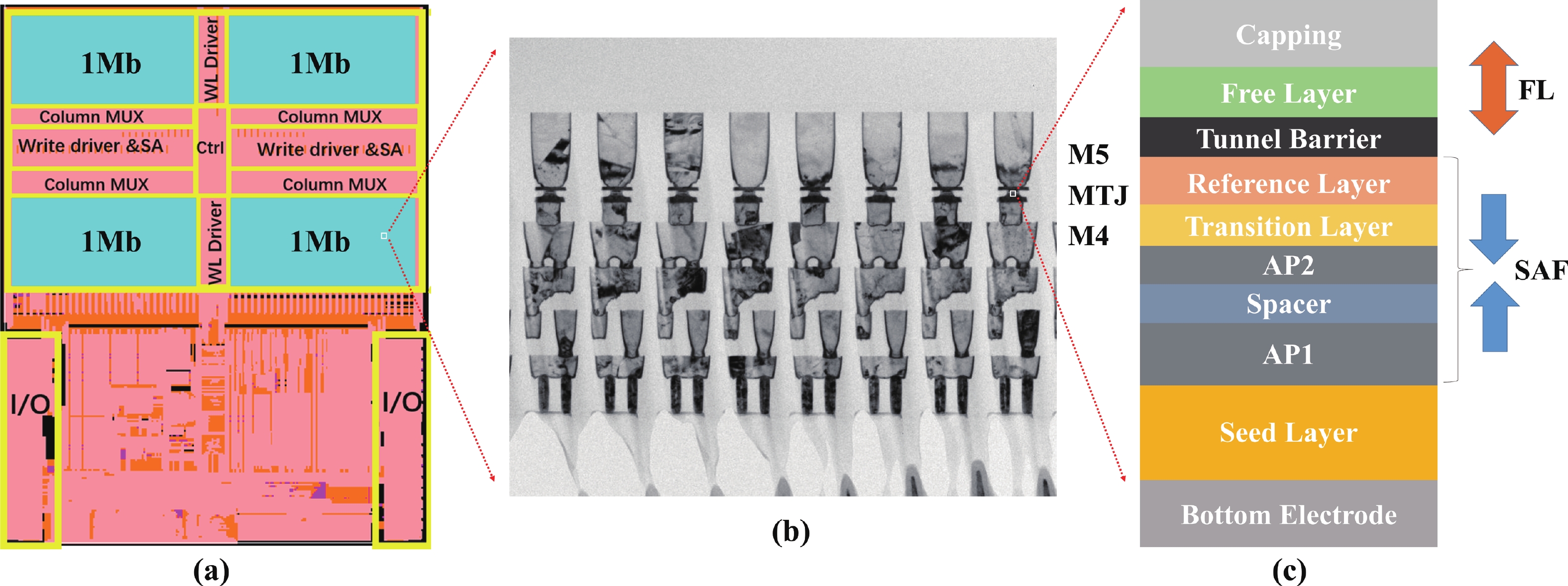
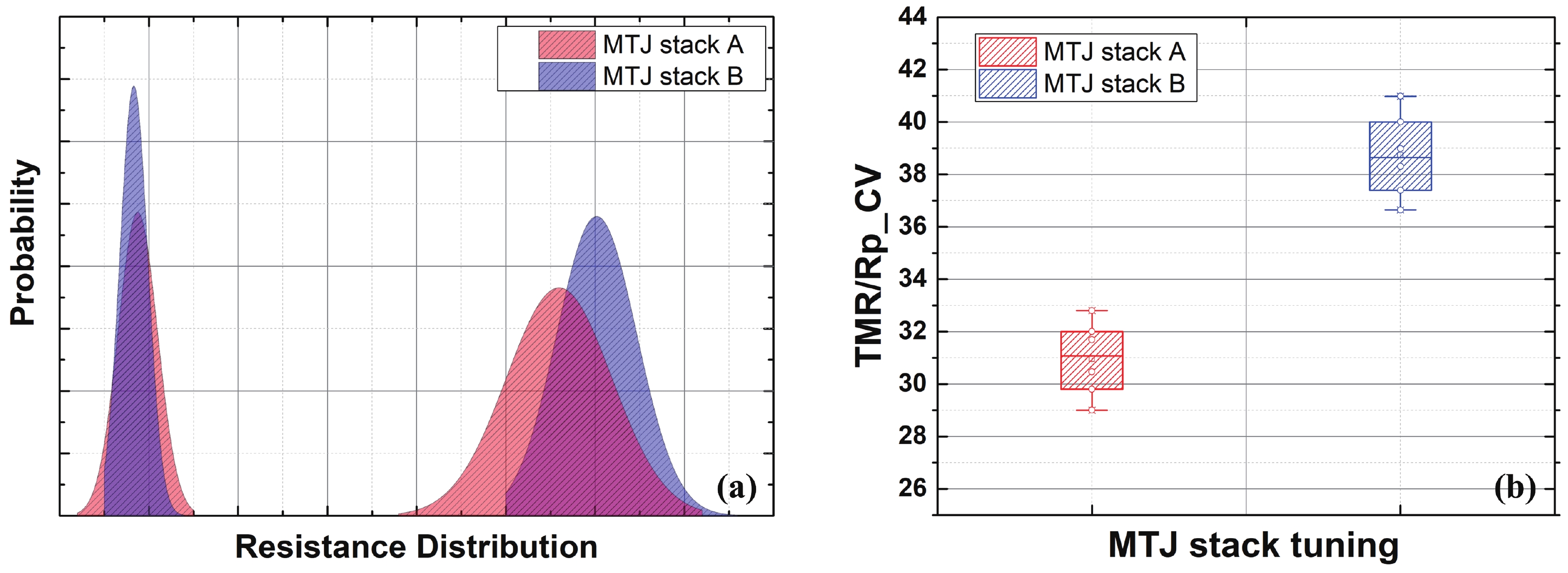
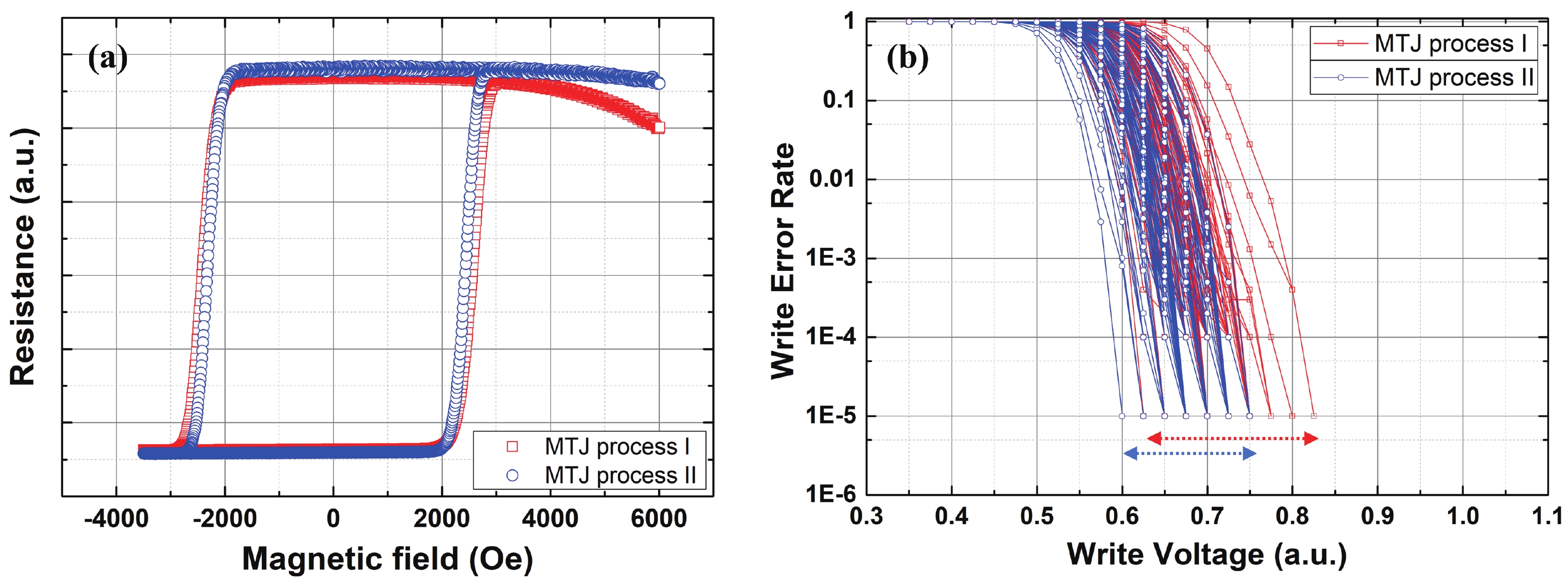
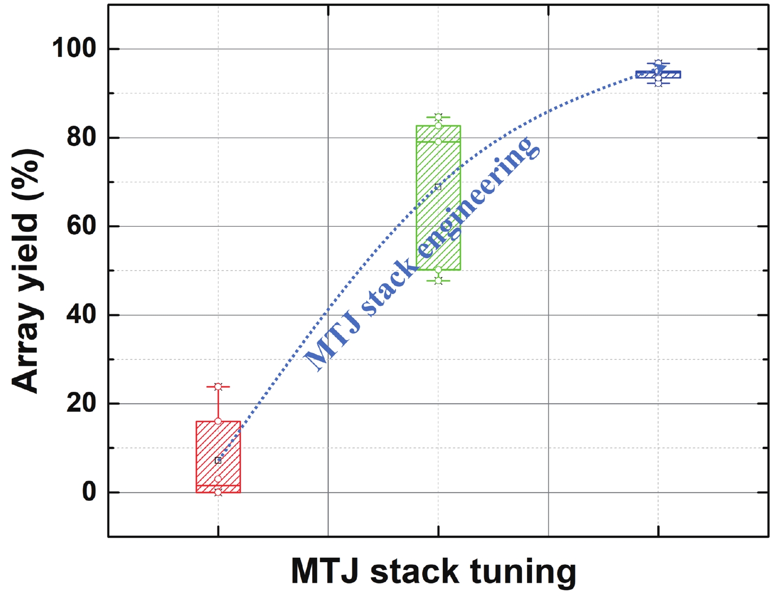
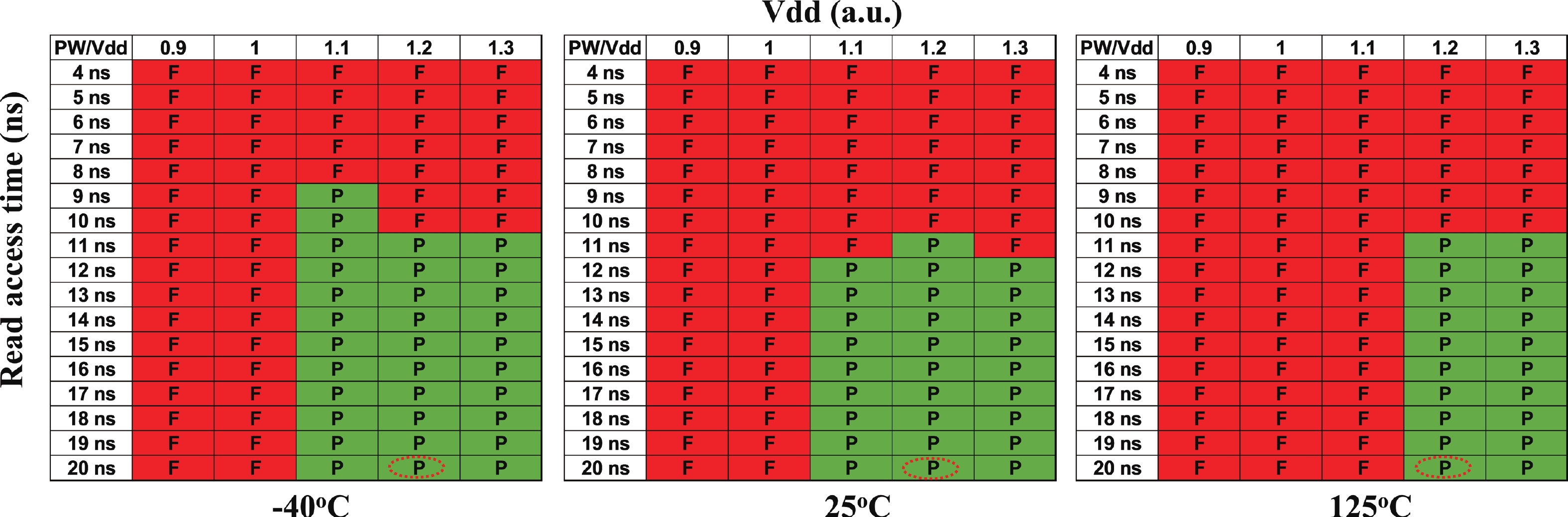
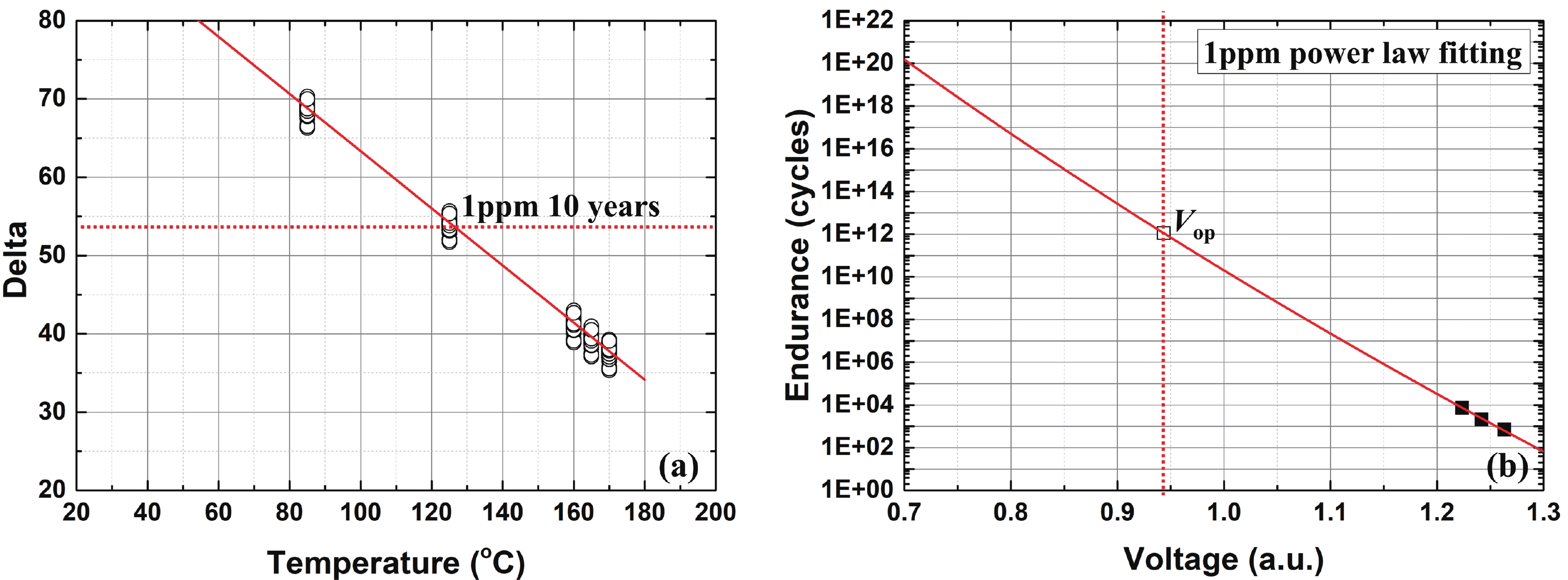
Magnetic tunnel junction (MTJ) based spin transfer torque magnetic random access memory (STT-MRAM) has been gaining tremendous momentum in high performance microcontroller (MCU) applications. As eFlash-replacement type MRAM approaches mass production, there is an increasing demand for non-volatile RAM (nvRAM) technologies that offer fast write speed and high endurance. In this work, we demonstrate highly reliable 4 Mb nvRAM type MRAM suitable for industry and auto grade-1 applications. This nvRAM features retention over 10 years at 125 °C, endurance of 1 × 10¹² cycles with 20 ns write speed, making it ideal for applications requiring both high speed and broad temperature ranges. By employing innovative MTJ materials, process engineering, and a co-optimization of process and design, reliable read and write performance across the full temperature range between −40 to 125 °C, and array yield that meets sub-1 ppm error rate was significantly improved from 0 to above 95%, a concrete step toward applications.

J. Semicond.
2025, 46(3): 032401 doi: 10.1088/1674-4926/24100028

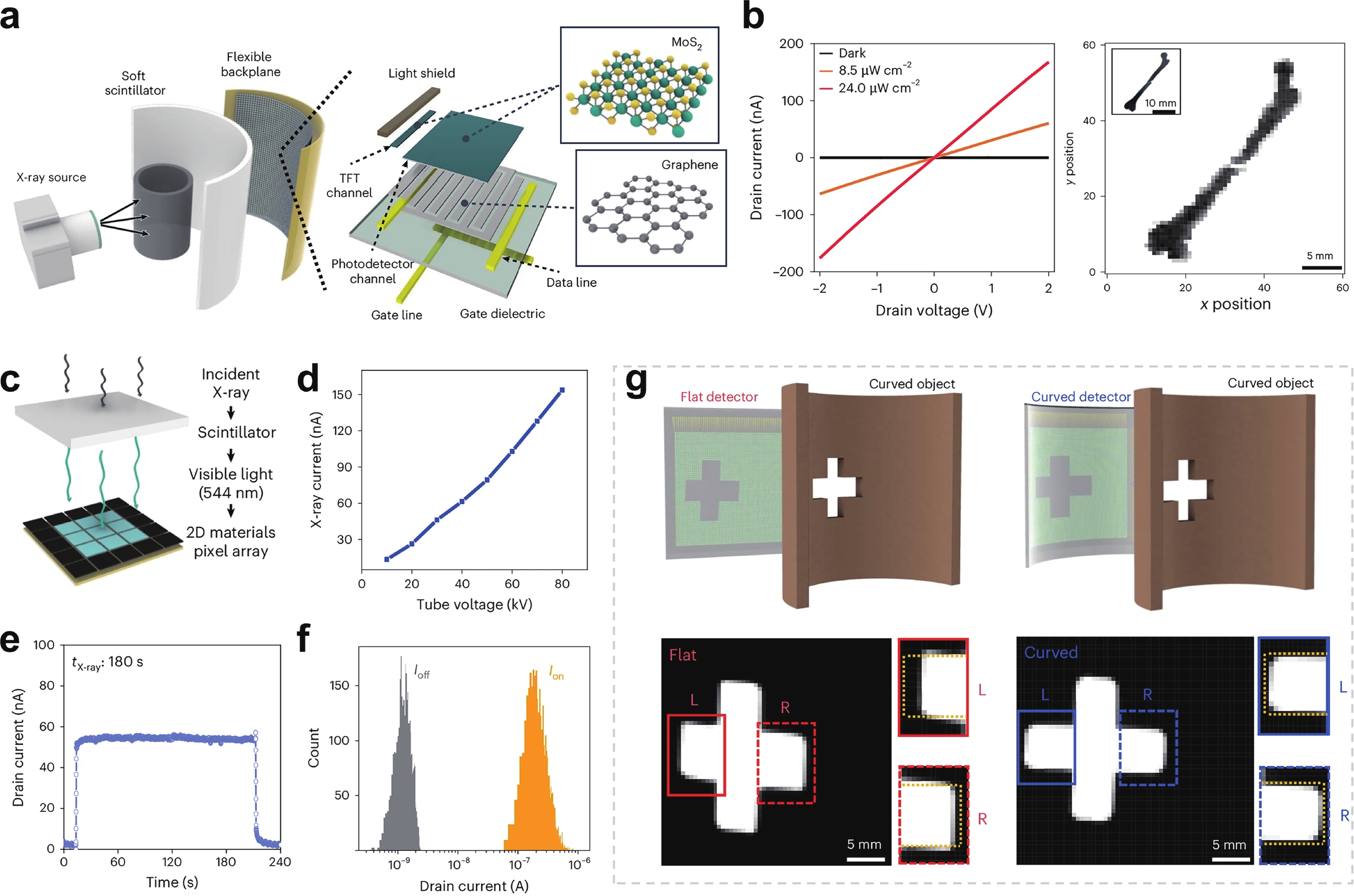
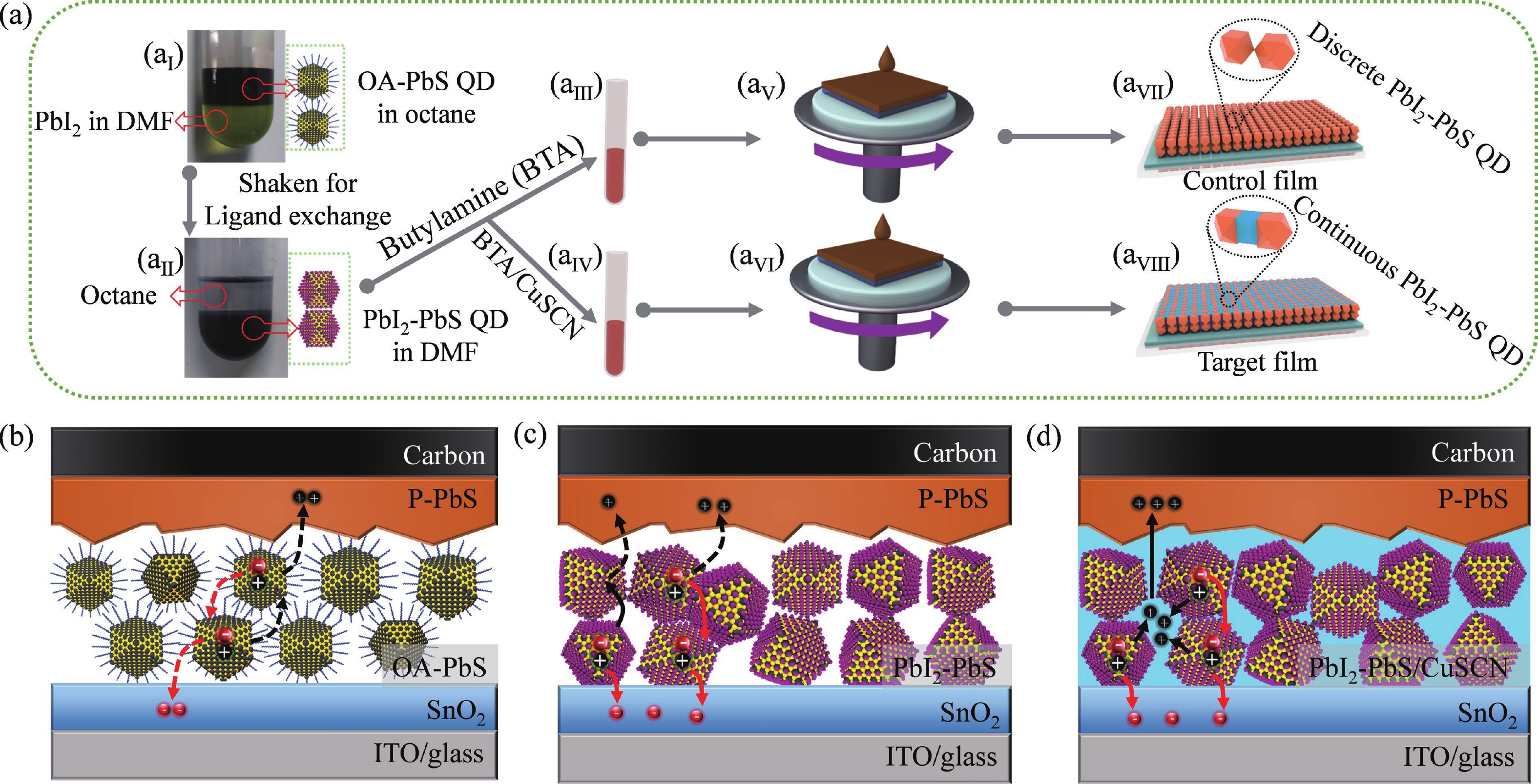
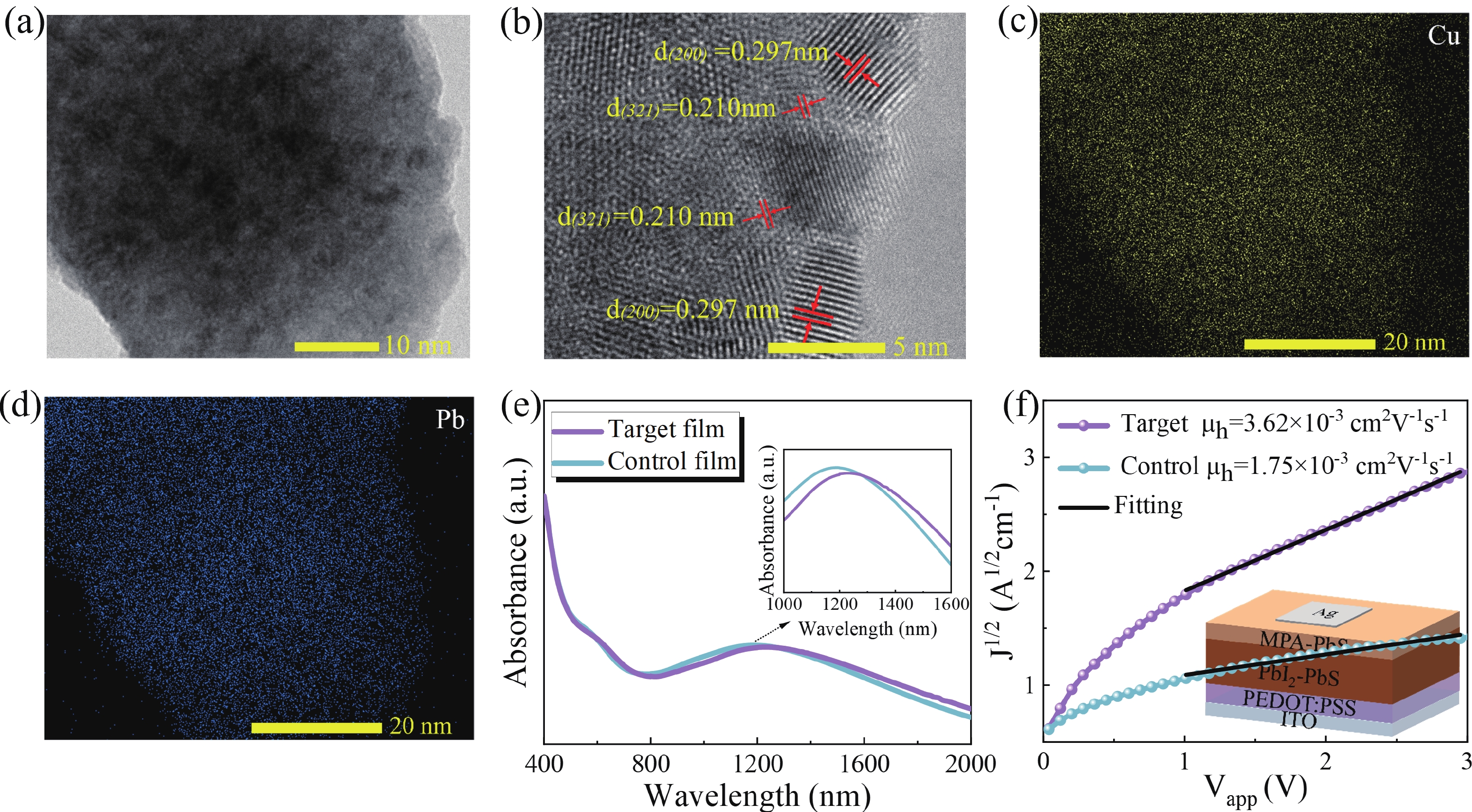
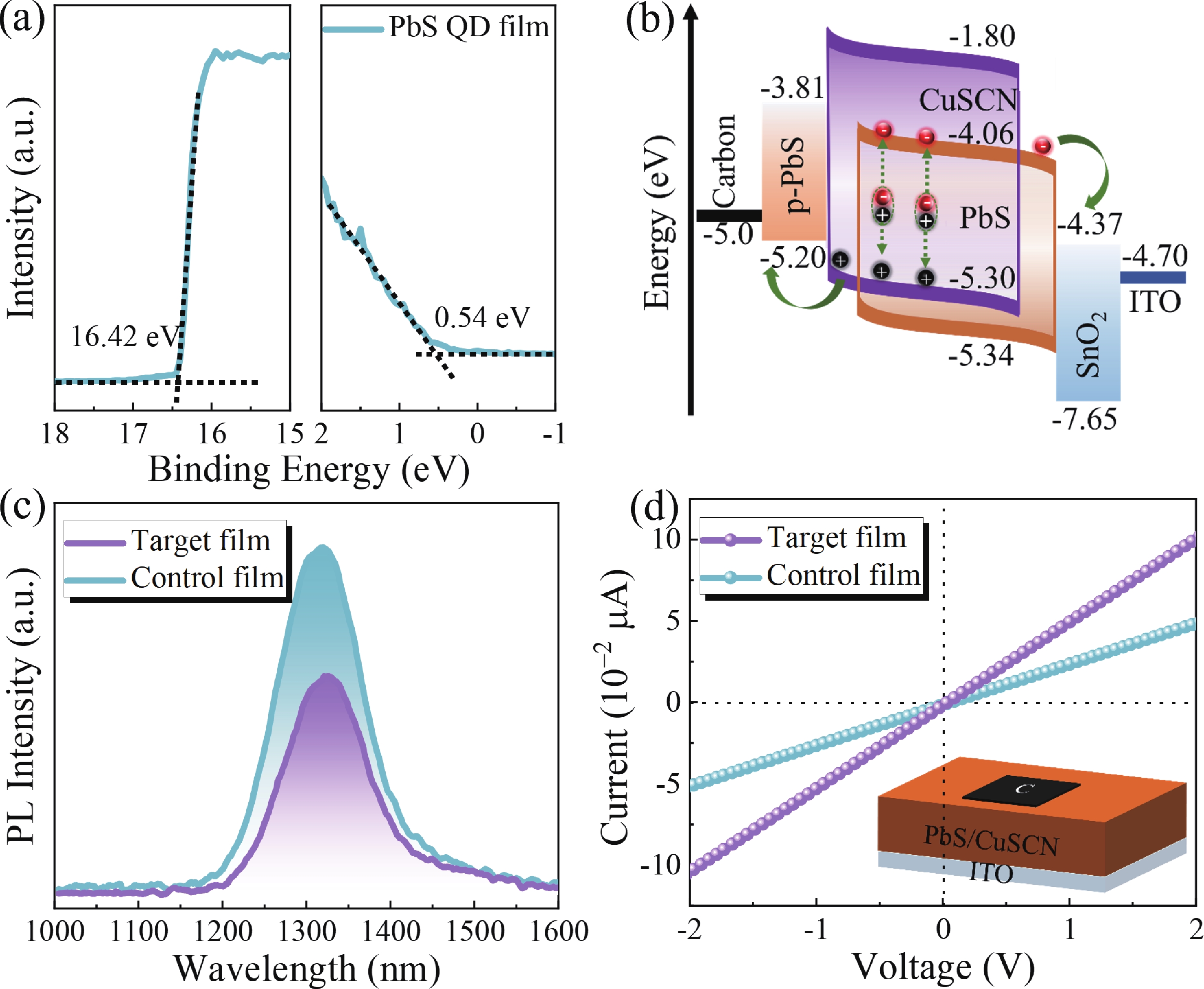
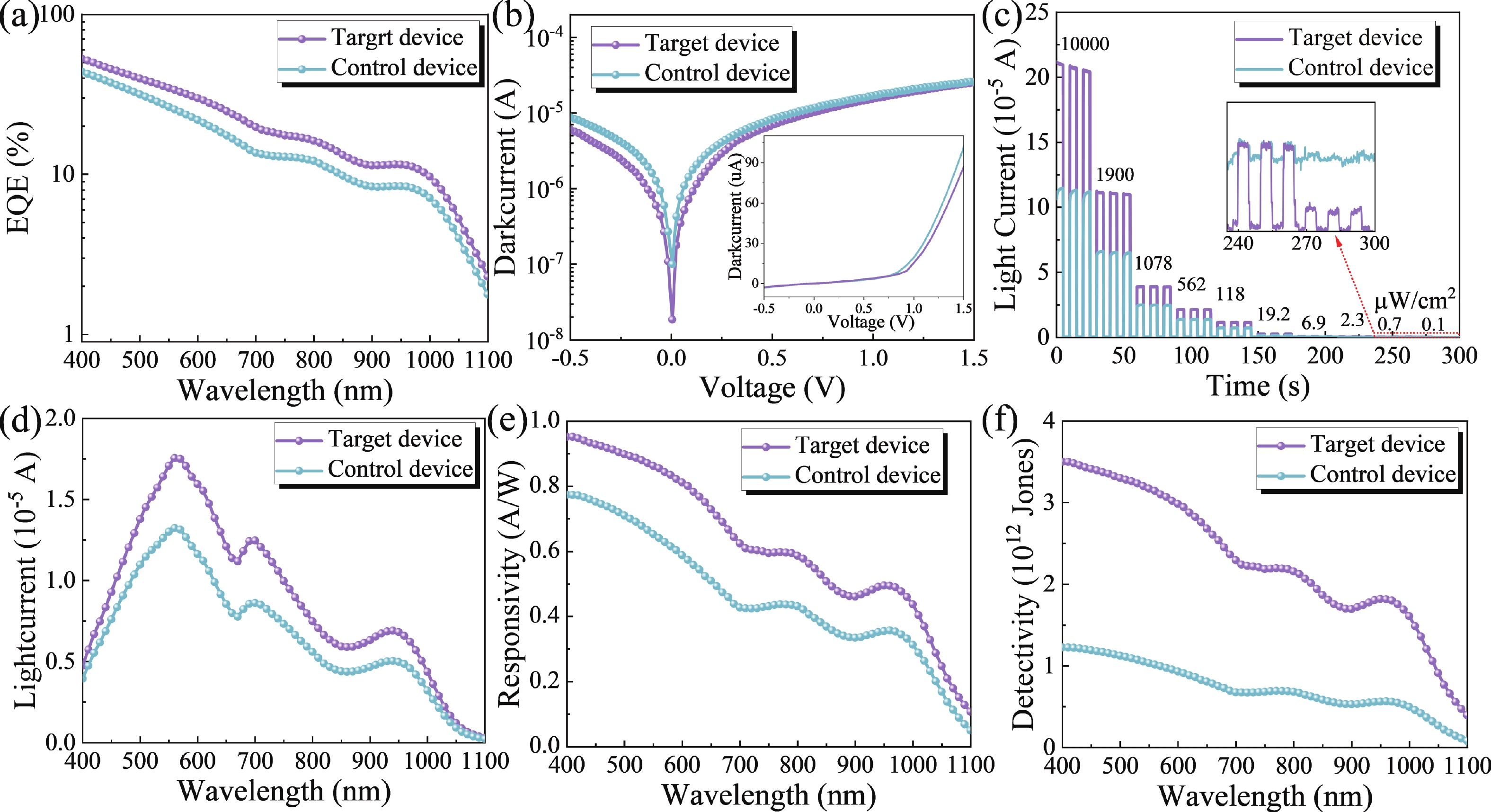
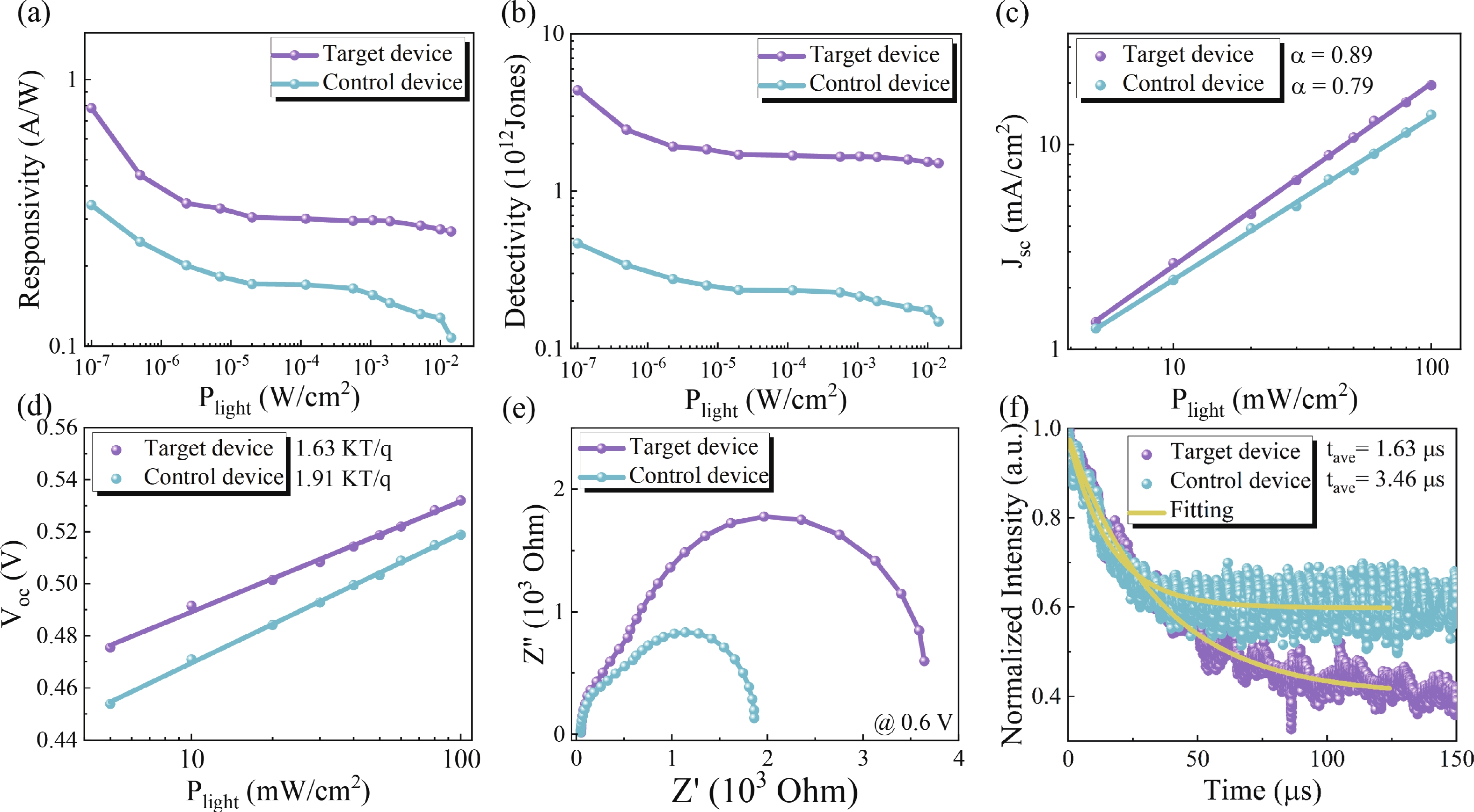
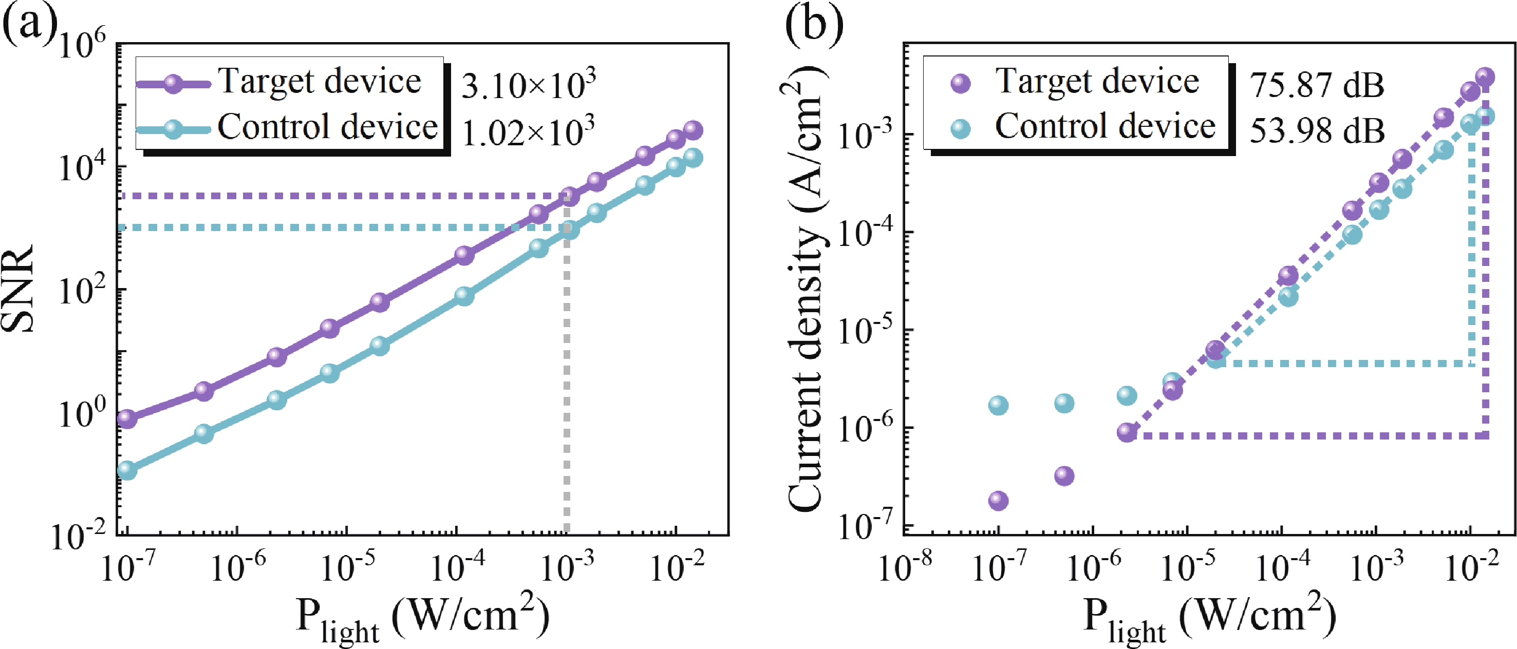
Quantum dot (QD)-based infrared photodetector is a promising technology that can implement current monitoring, imaging and optical communication in the infrared region. However, the photodetection performance of self-powered QD devices is still limited by their unfavorable charge carrier dynamics due to their intrinsically discrete charge carrier transport process. Herein, we strategically constructed semiconducting matrix in QD film to achieve efficient charge transfer and extraction. The p-type semiconducting CuSCN was selected as energy-aligned matrix to match the n-type colloidal PbS QDs that was used as proof-of-concept. Note that the PbS QD/CuSCN matrix not only enables efficient charge carrier separation and transfer at nano-interfaces but also provides continuous charge carrier transport pathways that are different from the hoping process in neat QD film, resulting in improved charge mobility and derived collection efficiency. As a result, the target structure delivers high specific detectivity of 4.38 × 10¹² Jones and responsivity of 782 mA/W at 808 nm, which is superior than that of the PbS QD-only photodetector (4.66 × 10¹¹ Jones and 338 mA/W). This work provides a new structure candidate for efficient colloidal QD based optoelectronic devices.
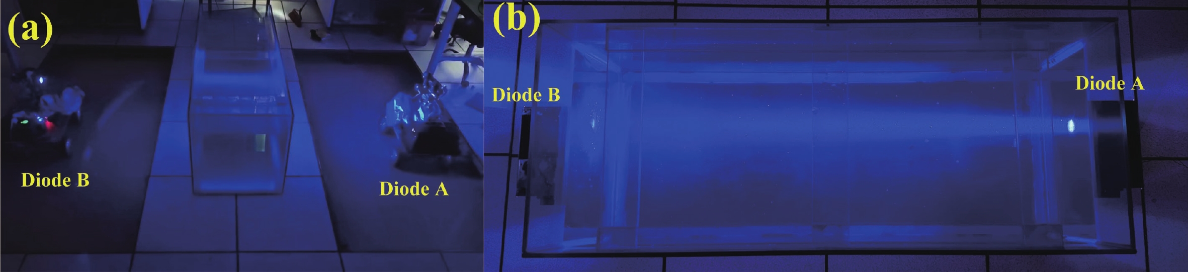
Mobile blue-light communication over a signal optical path using a time-division multiplexing scheme
J. Semicond.
2025, 46(3): 032402 doi: 10.1088/1674-4926/24080022
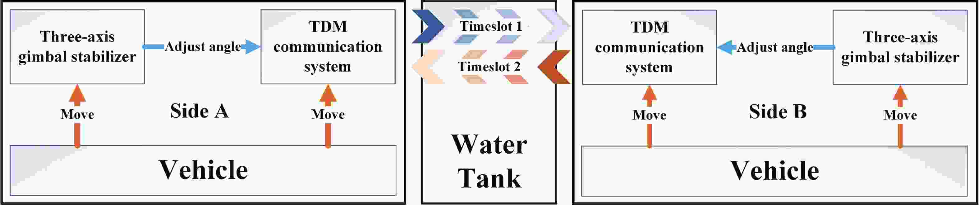
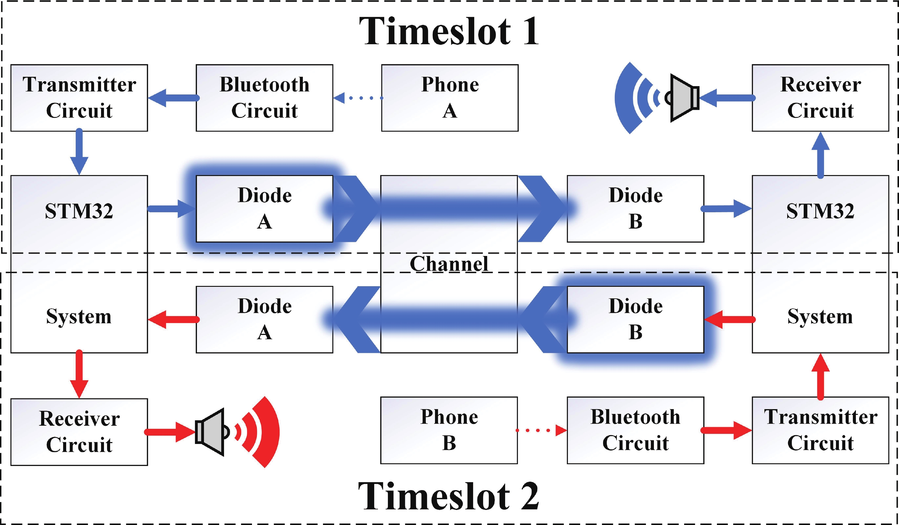
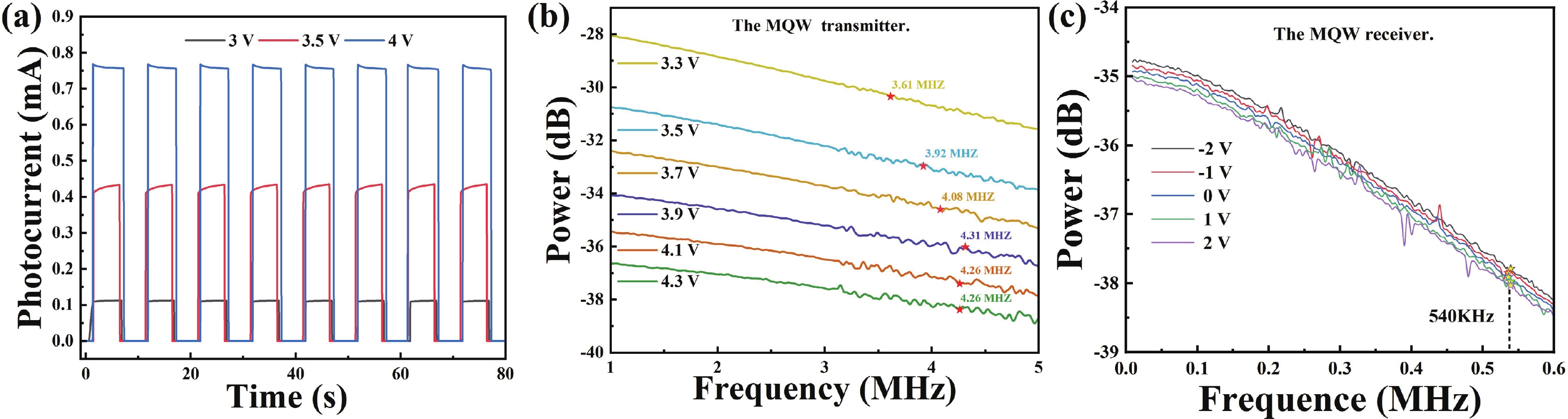
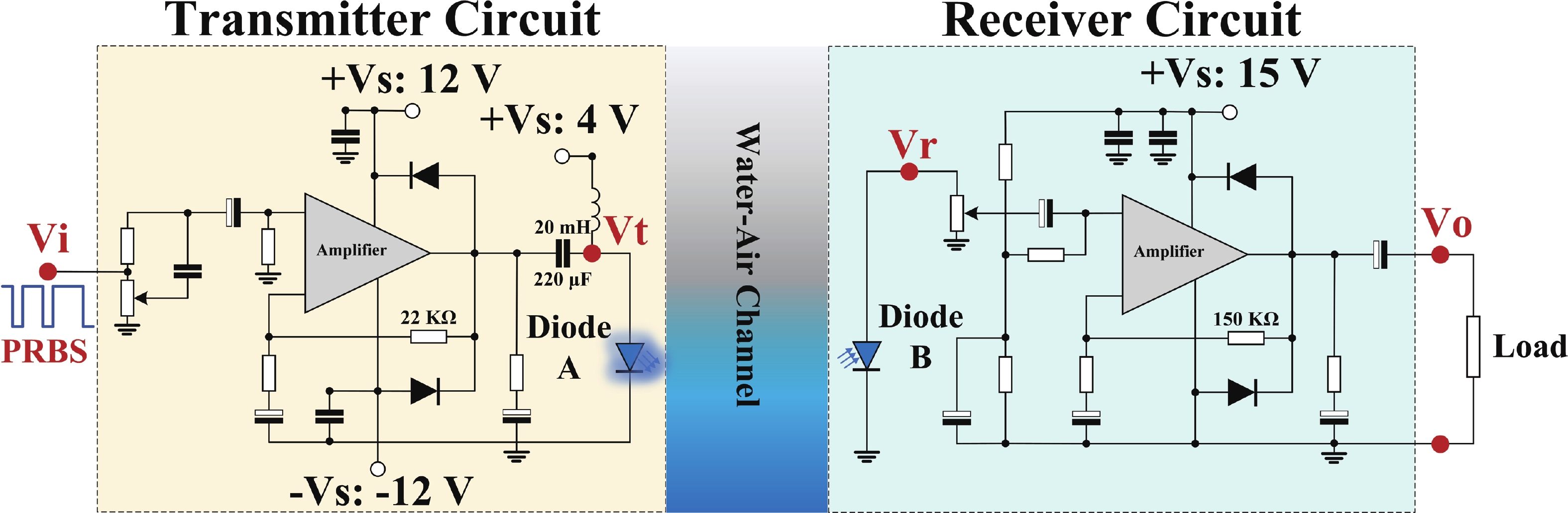
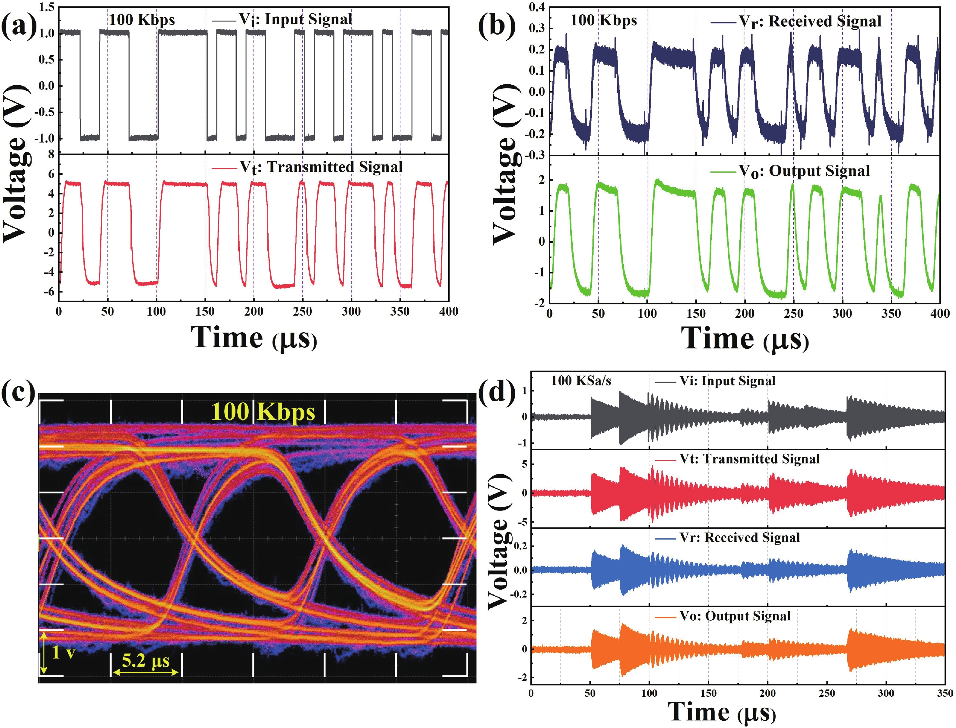
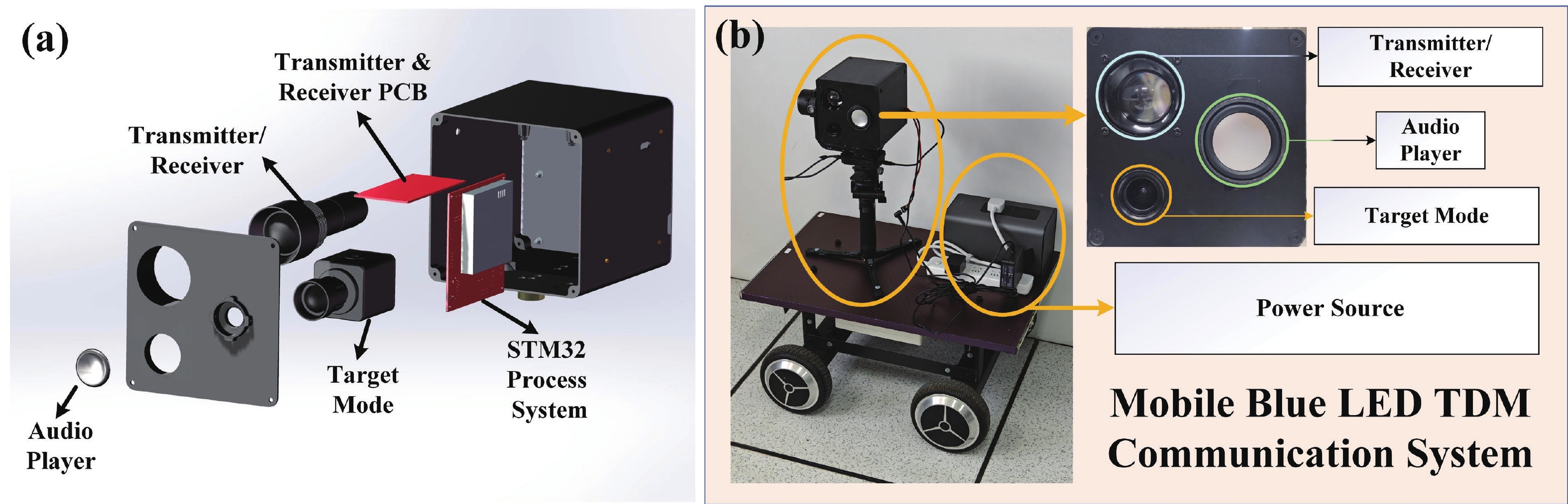
Multiple quantum well (MQW) Ⅲ-nitride diodes that can simultaneously emit and detect light feature an overlapping region between their electroluminescence and responsivity spectra, which allows them to be simultaneously used as both a transmitter and a receiver in a wireless light communication system. Here, we demonstrate a mobile light communication system using a time-division multiplexing (TDM) scheme to achieve bidirectional data transmission via the same optical channel. Two identical blue MQW diodes are defined by software as a transmitter or a receiver. To address the light alignment issue, an image identification module integrated with a gimbal stabilizer is used to automatically detect the locations of moving targets; thus, underwater audio communication is realized via a mobile blue-light TDM communication mode. This approach not only uses a single link but also integrates mobile nodes in a practical network.
J. Semicond.
2025, 46(3): 032403 doi: 10.1088/1674-4926/24090033
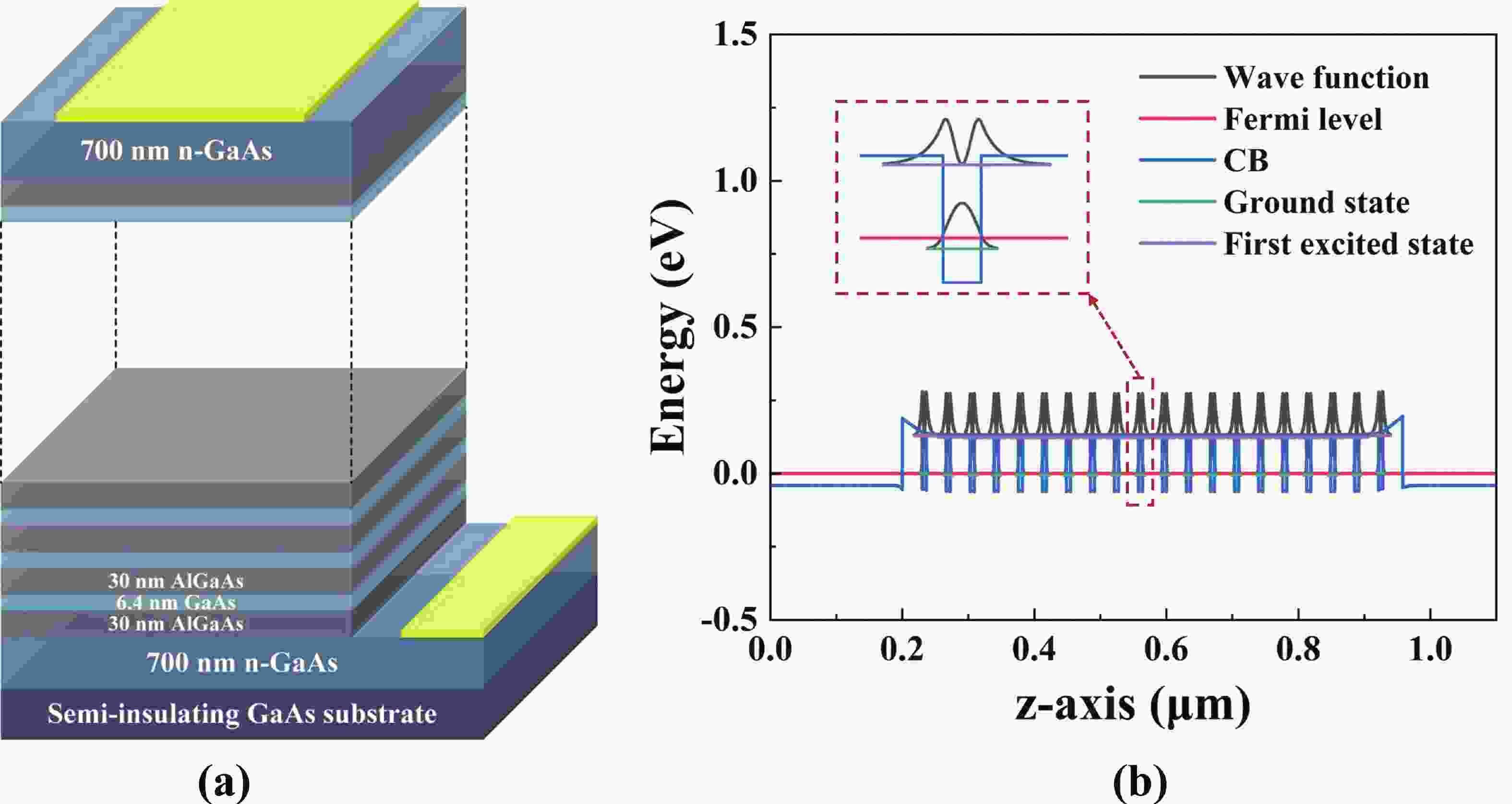
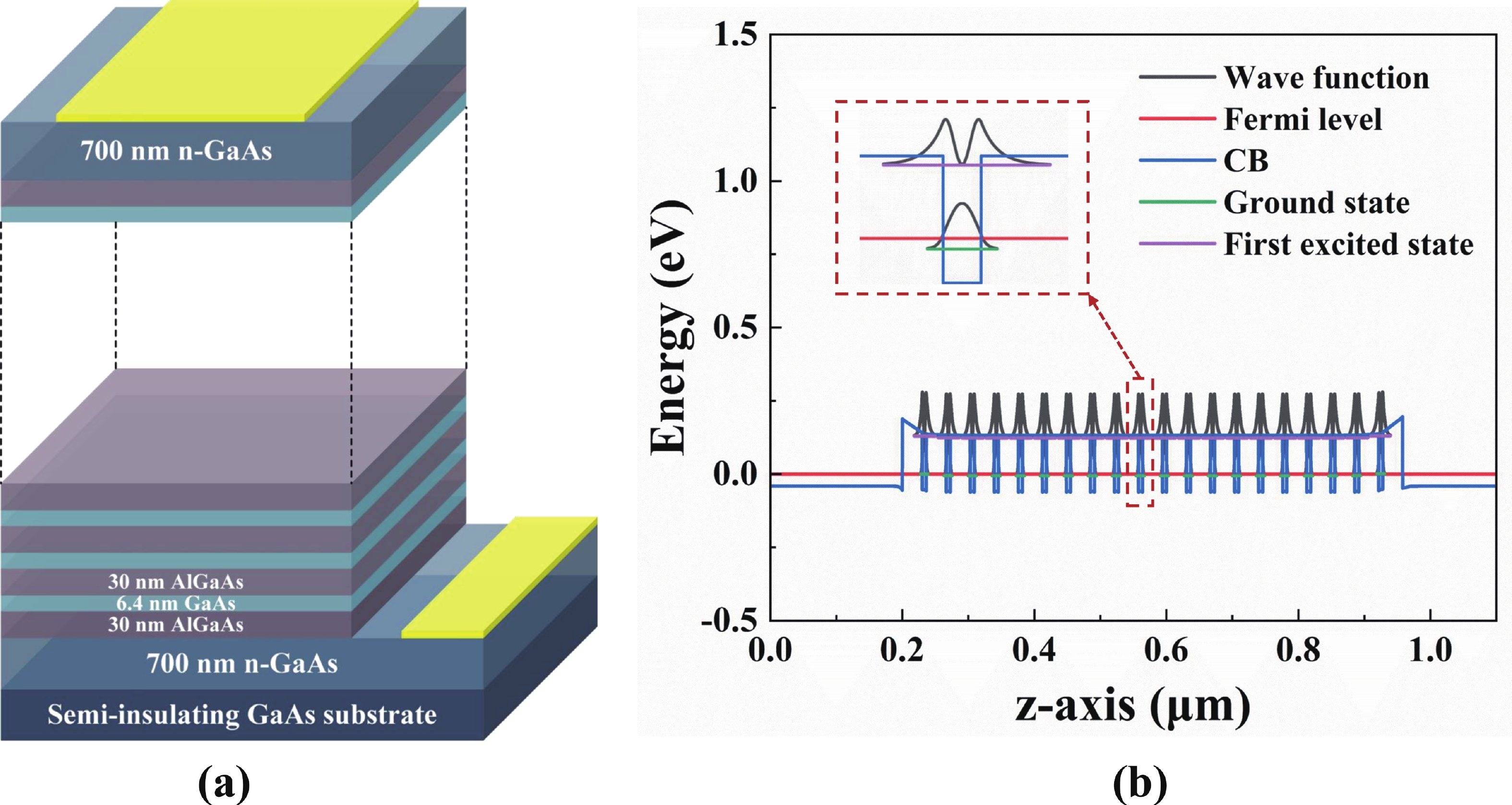
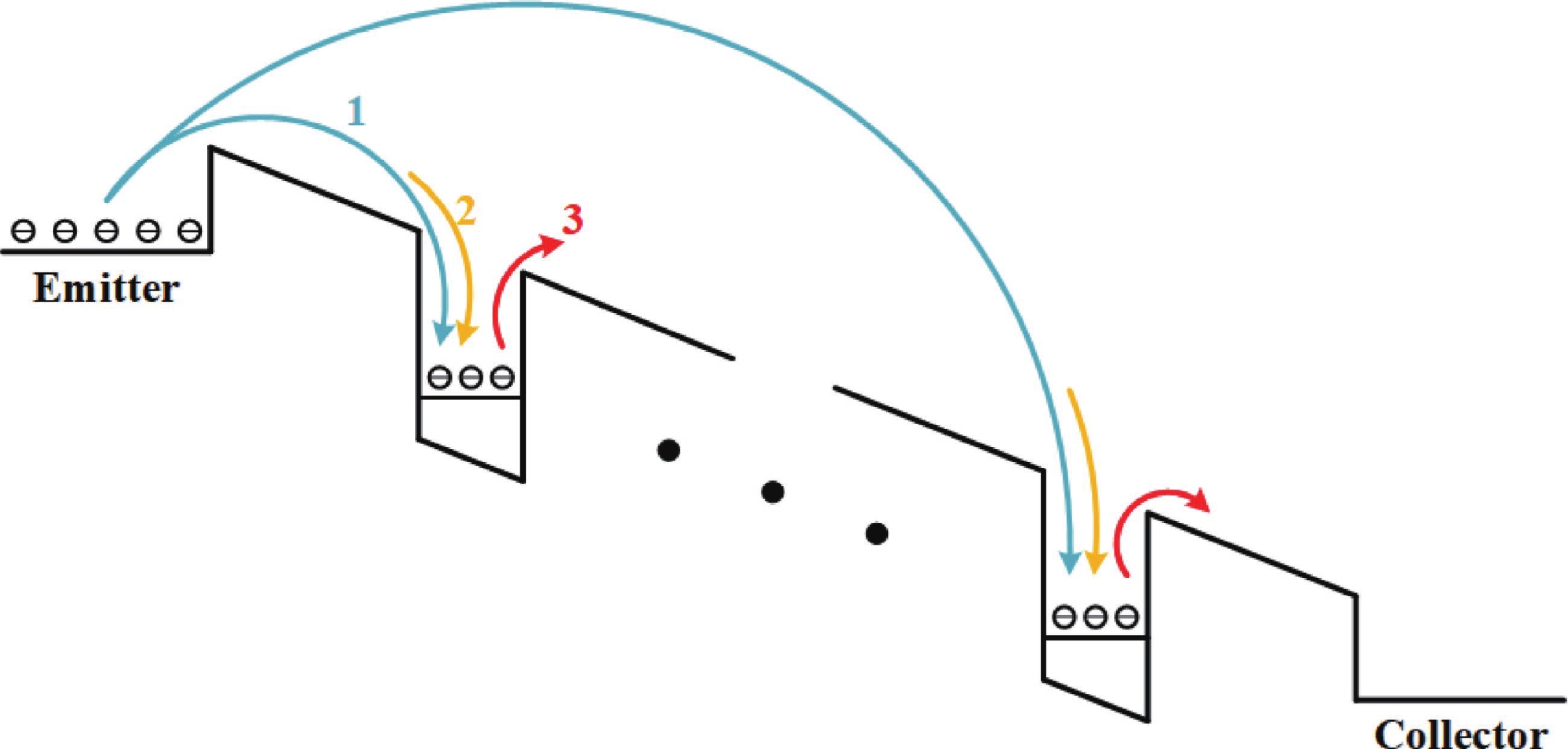
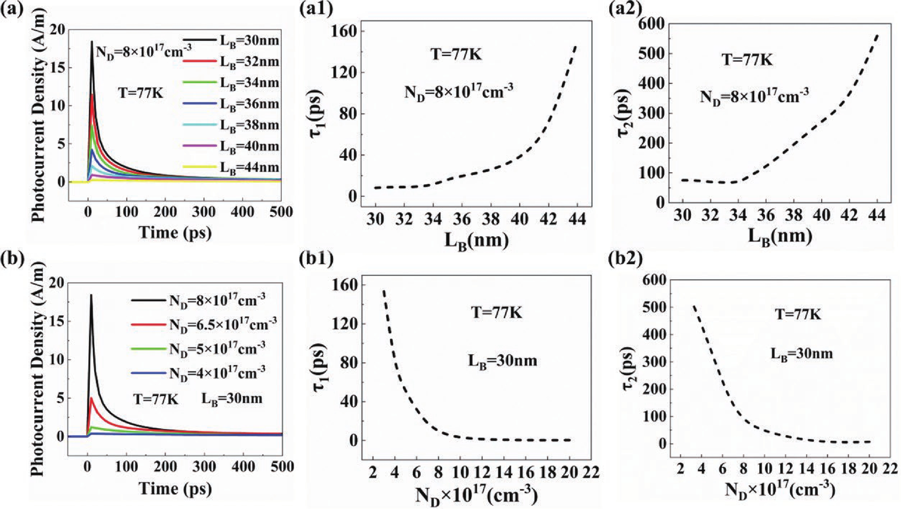
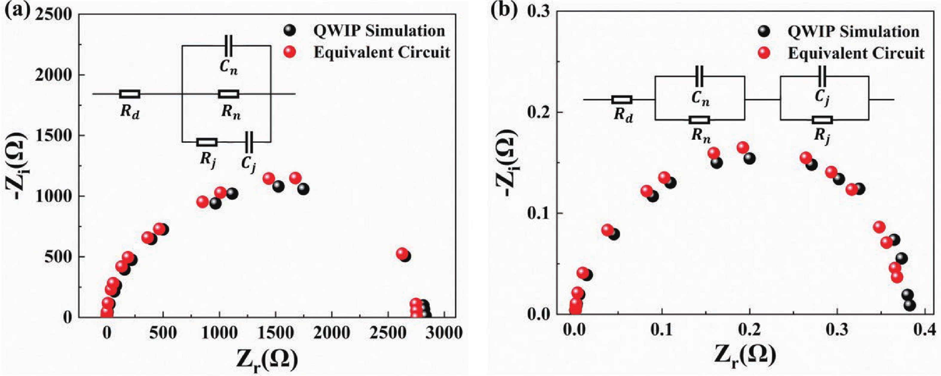
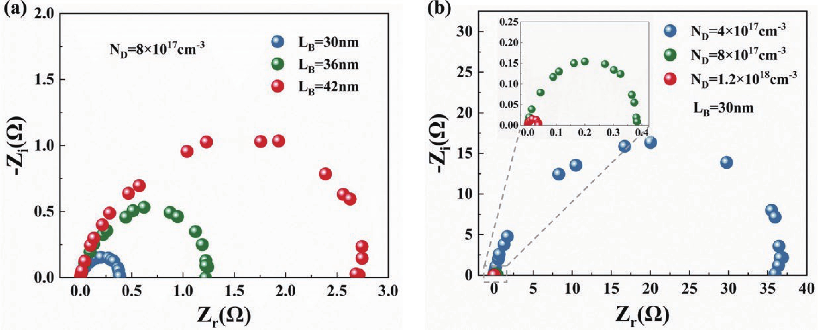
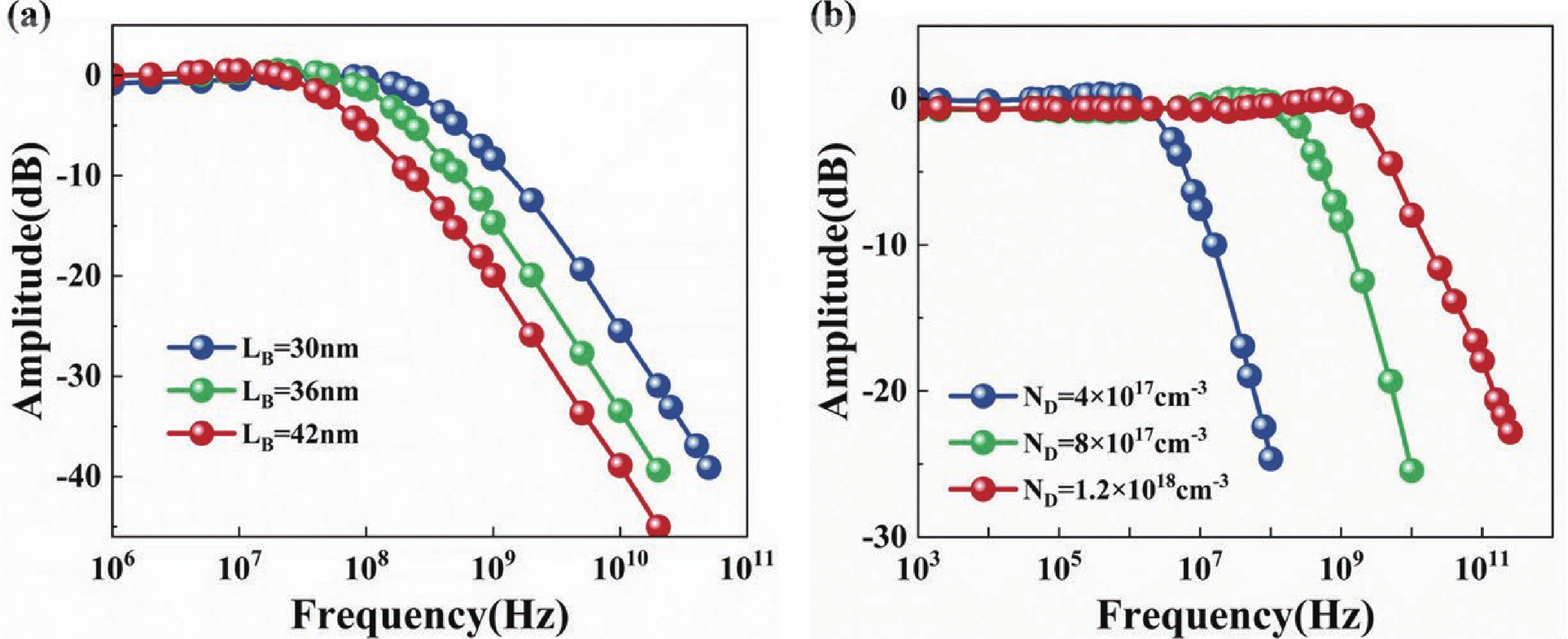
Quantum well infrared photodetectors (QWIPs) based on intersubband transitions hold significant potential for high bandwidth operation. In this work, we establish a carrier transport optimization model incorporating electron injection at the emitter to investigate the carrier dynamics time and impedance spectroscopy in GaAs/AlGaAs QWIPs. Our findings provide novel evidence that the escape time of electrons is the key limiting factor for the 3-dB bandwidth of QWIPs. Moreover, to characterize the impact of carrier dynamics time and non-equilibrium space charge region on impedance, we developed an equivalent circuit model where depletion region resistance and capacitance are employed to describe non-equilibrium space charge region. Using this model, we discovered that under illumination, both net charge accumulation caused by variations in carrier dynamics times within quantum wells and changes in width of non-equilibrium space charge region exert different dominant influences on depletion region capacitance at various doping concentrations.
J. Semicond.
2025, 46(3): 032501 doi: 10.1088/1674-4926/24100041

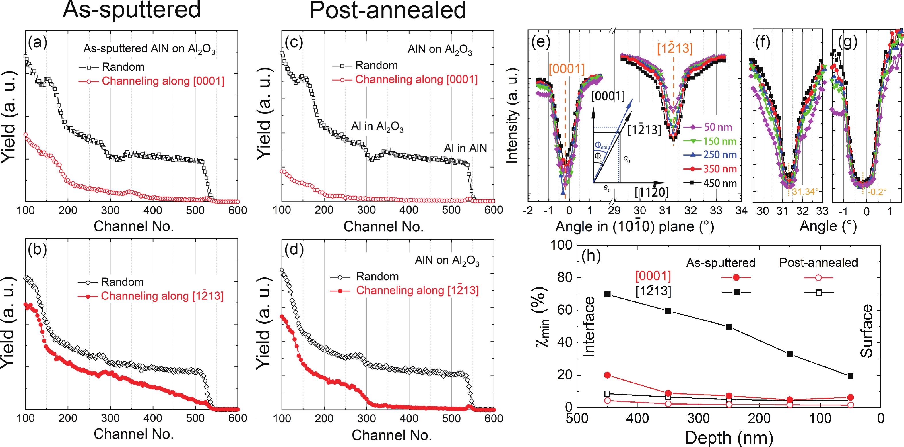
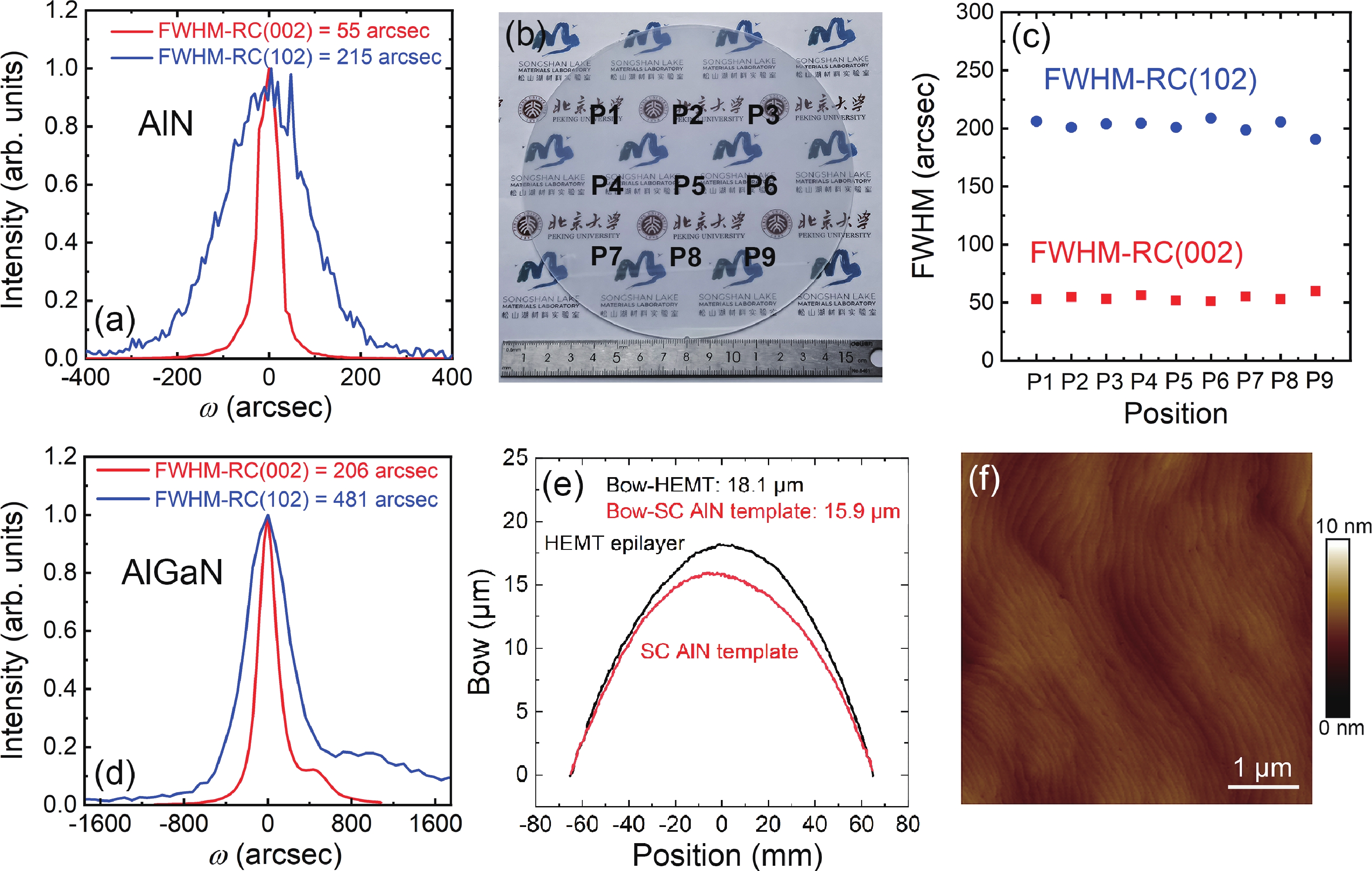
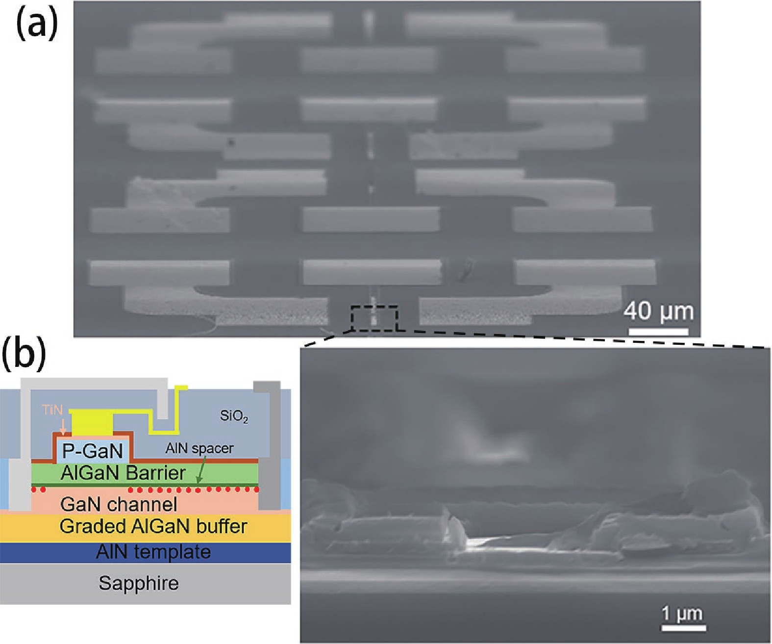
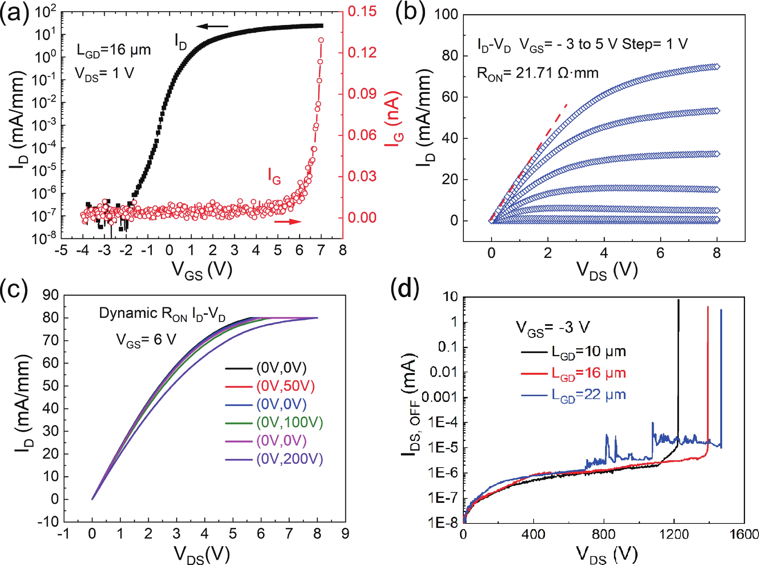
In the present work, the high uniform 6-inch single-crystalline AlN template is successfully achieved by high temperature annealing technique, which opens up the path towards industrial application in power device. Moreover, the outstanding crystalline-quality is confirmed by Rutherford backscattering spectrometry (RBS). In accompanied with the results from X-ray diffraction, the RBS results along both [0001] and $ [1\bar{2}13] $ reveal that the in-plane lattice is effectively reordered by high temperature annealing. In addition, the constant Φepi angle between [0001] and $ [1\bar{2}13] $ at different depths of 31.54° confirms the uniform compressive strain inside the AlN region. Benefitting from the excellent crystalline quality of AlN template, we can epitaxially grow the enhanced-mode high electron mobility transistor (HEMT) with a graded AlGaN buffer as thin as only ~300 nm. Such an ultra-thin AlGaN buffer layer results in the wafer-bow as low as 18.1 μm in 6-inch wafer scale. The fabricated HEMT devices with 16 μm-LGD exhibits a threshold voltage (VTH) of 1.1 V and a high OFF-state breakdown voltage (VBD) over 1400 V. Furthermore, after 200 V high-voltage OFF-state stress, the current collapse is only 13.6%. Therefore, the advantages of both 6-inch size and excellent crystallinity announces the superiority of single-crystalline AlN template in low-cost electrical power applications.
J. Semicond.
2025, 46(3): 032701 doi: 10.1088/1674-4926/24080040
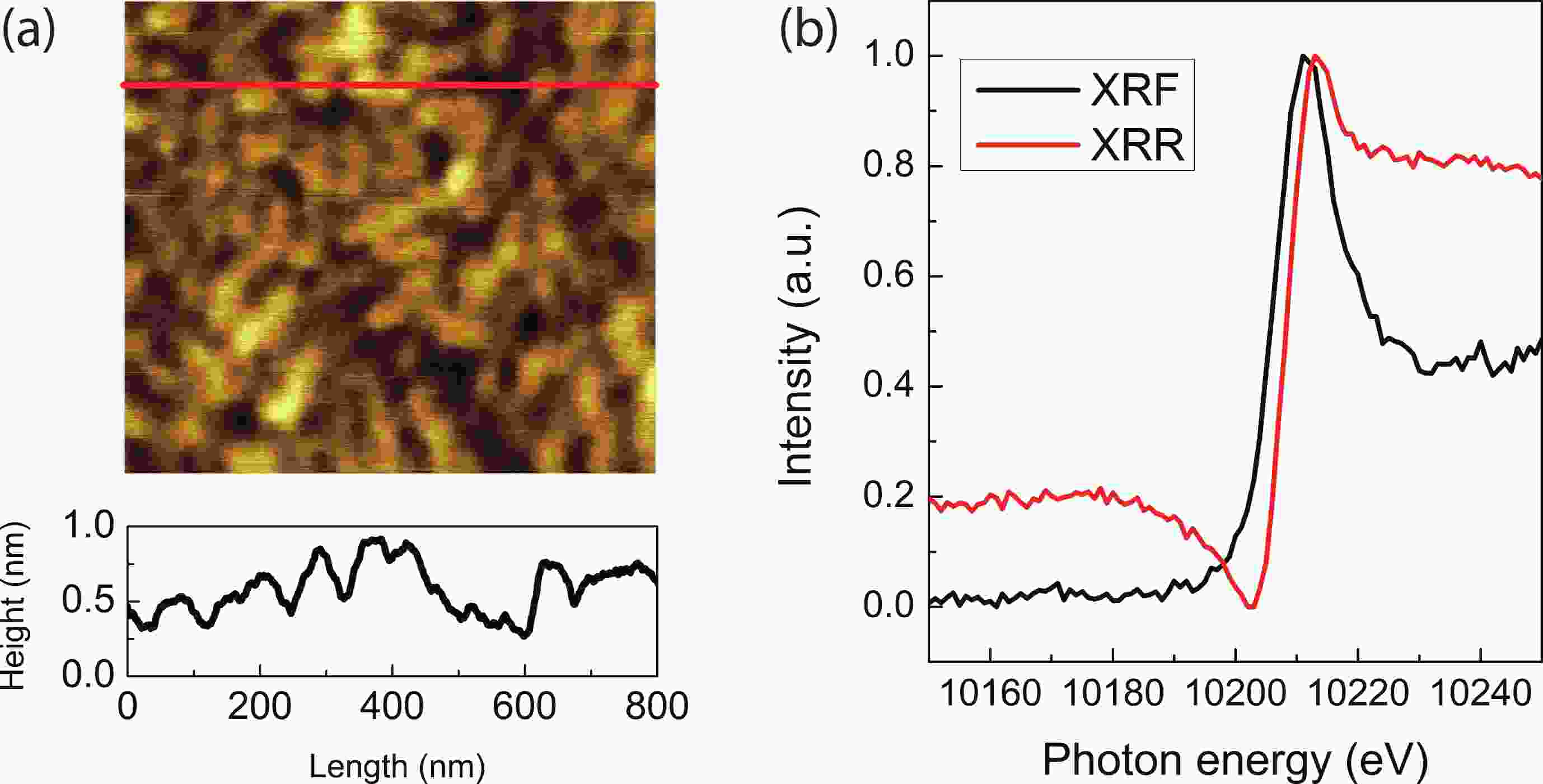
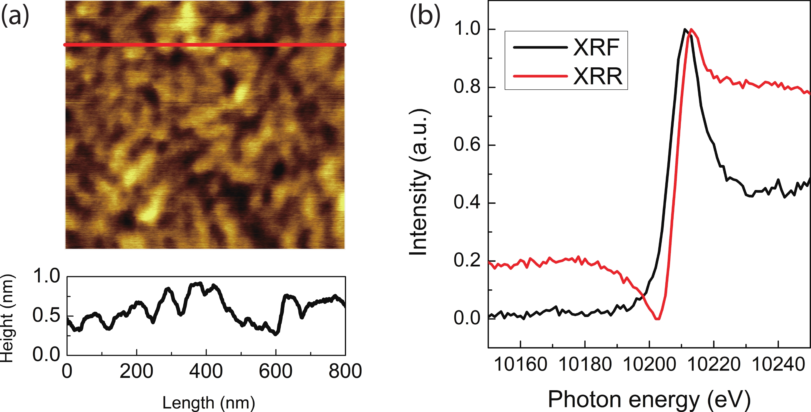
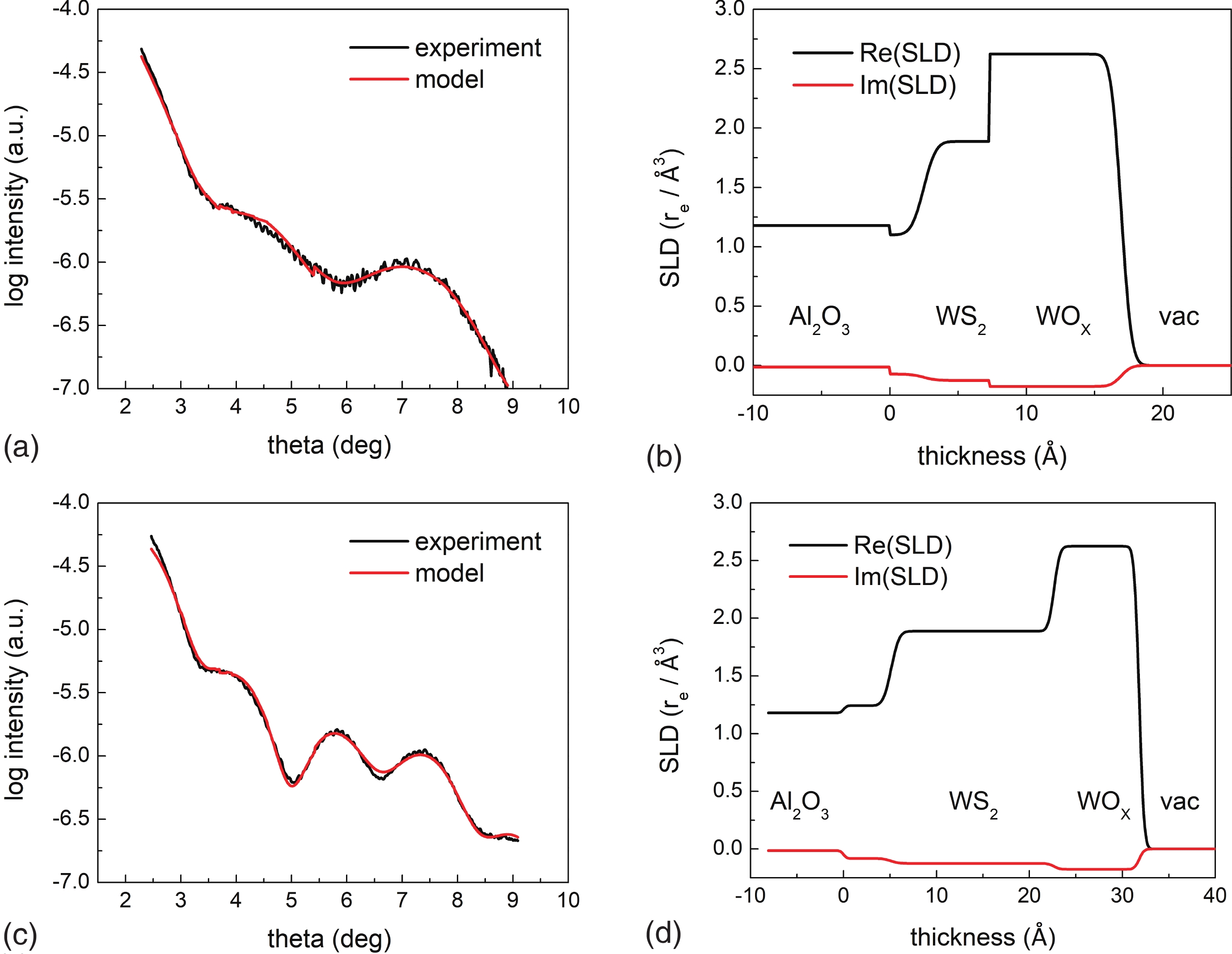
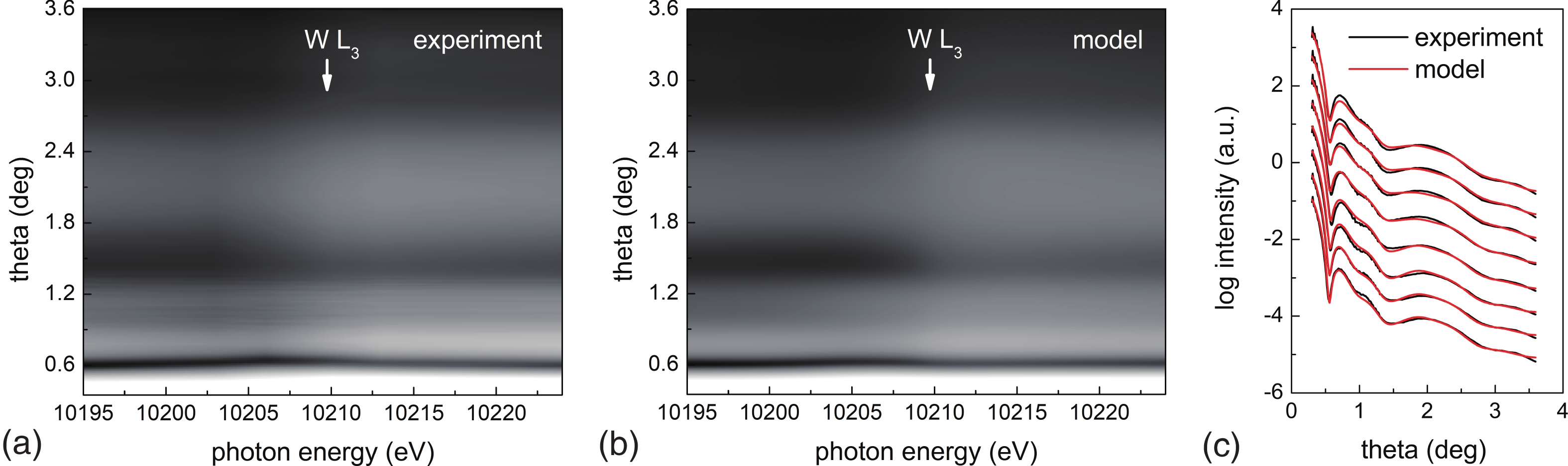
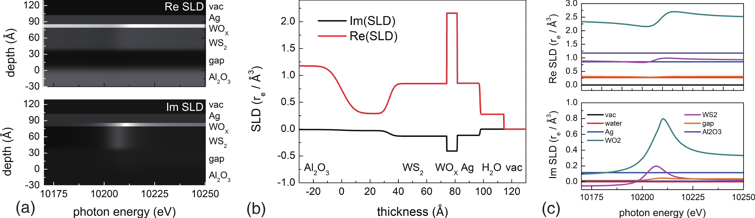
Synchrotron method of resonant X-ray reflectivity 2D mapping has been applied to study ultrathin epitaxial layers of WS2 grown by pulsed laser deposition on Al2O3(0001) substrates. The measurements were carried out across the L absorption edge of tungsten to perform depth-dependent element-selective analysis sensitive to potential chemical modification of the WS2 layer in ambient conditions. Despite the few monolayer thickness of the studied film, the experimentally measured maps of reflectance as a function of incident angle and photon energy turned out to be quite informative showing well-pronounced interference effects near W absorption edge at 10 210 eV. The synchrotron studies were complemented with conventional non-resonant reflectance measurements carried out in the laboratory at a fixed photon energy corresponding to Cu Kα emission. The reconstruction of the depth and energy dependent scattering length density within the studied multilayers was carried out using the OpenCL empowered fitting software utilizing spectral shaping algorithm which does not rely on the pre-measured reference absorption spectra. A thin WOx layer has been revealed at the surface of the WS2 layer pointing out to the effect of water assisted photo-oxidation reported in a number of works related to ultrathin layers of transition metal dichalcogenides.
J. Semicond.
2025, 46(3): 032702 doi: 10.1088/1674-4926/24080023
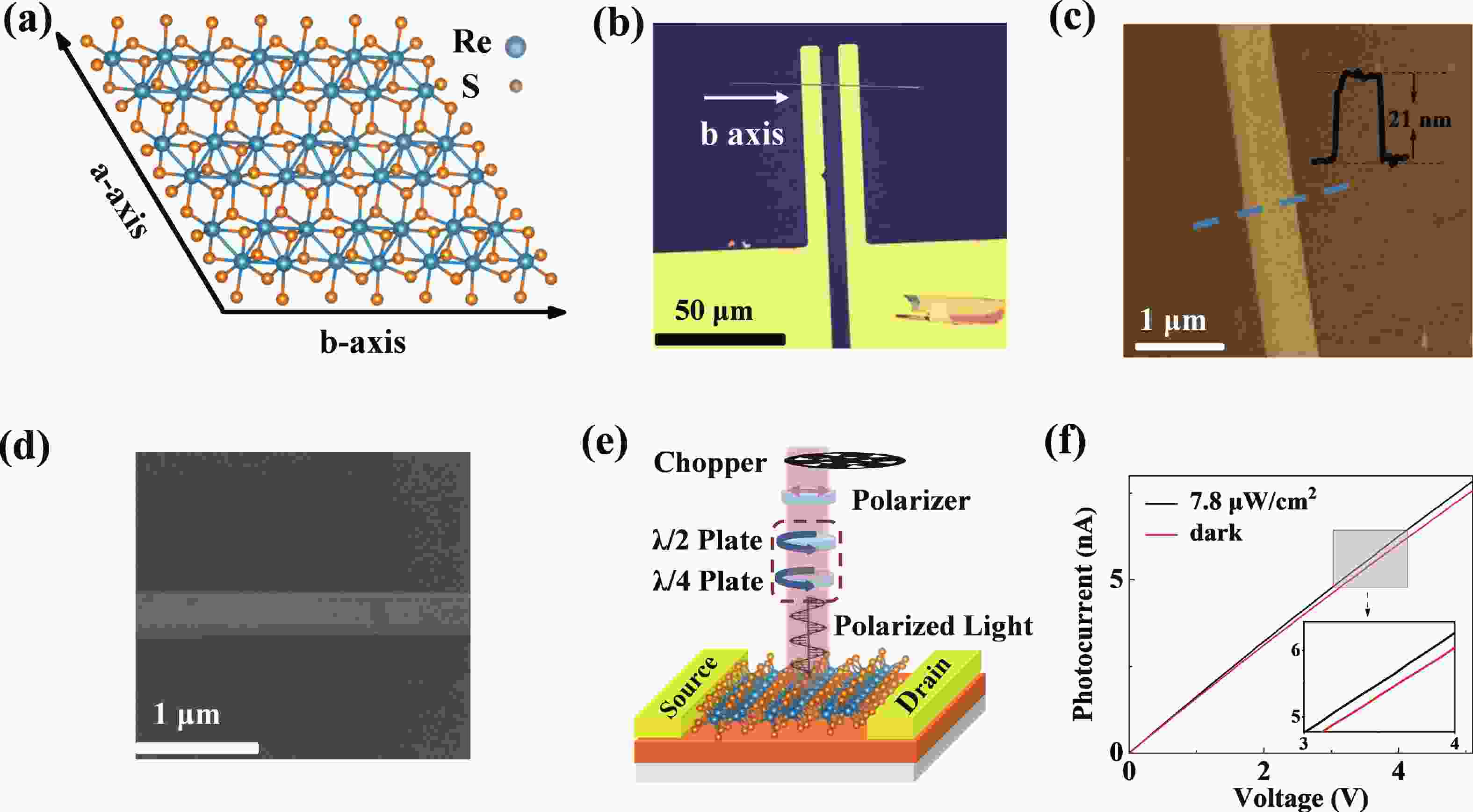
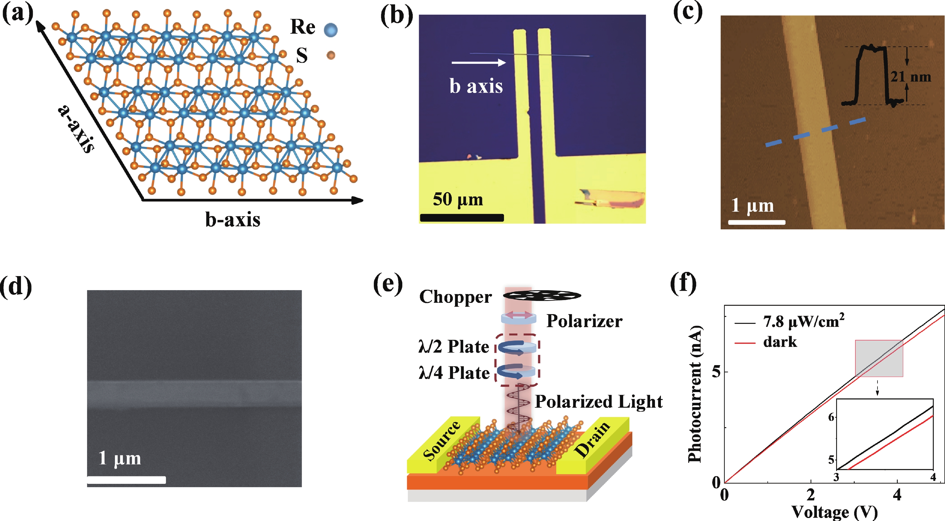
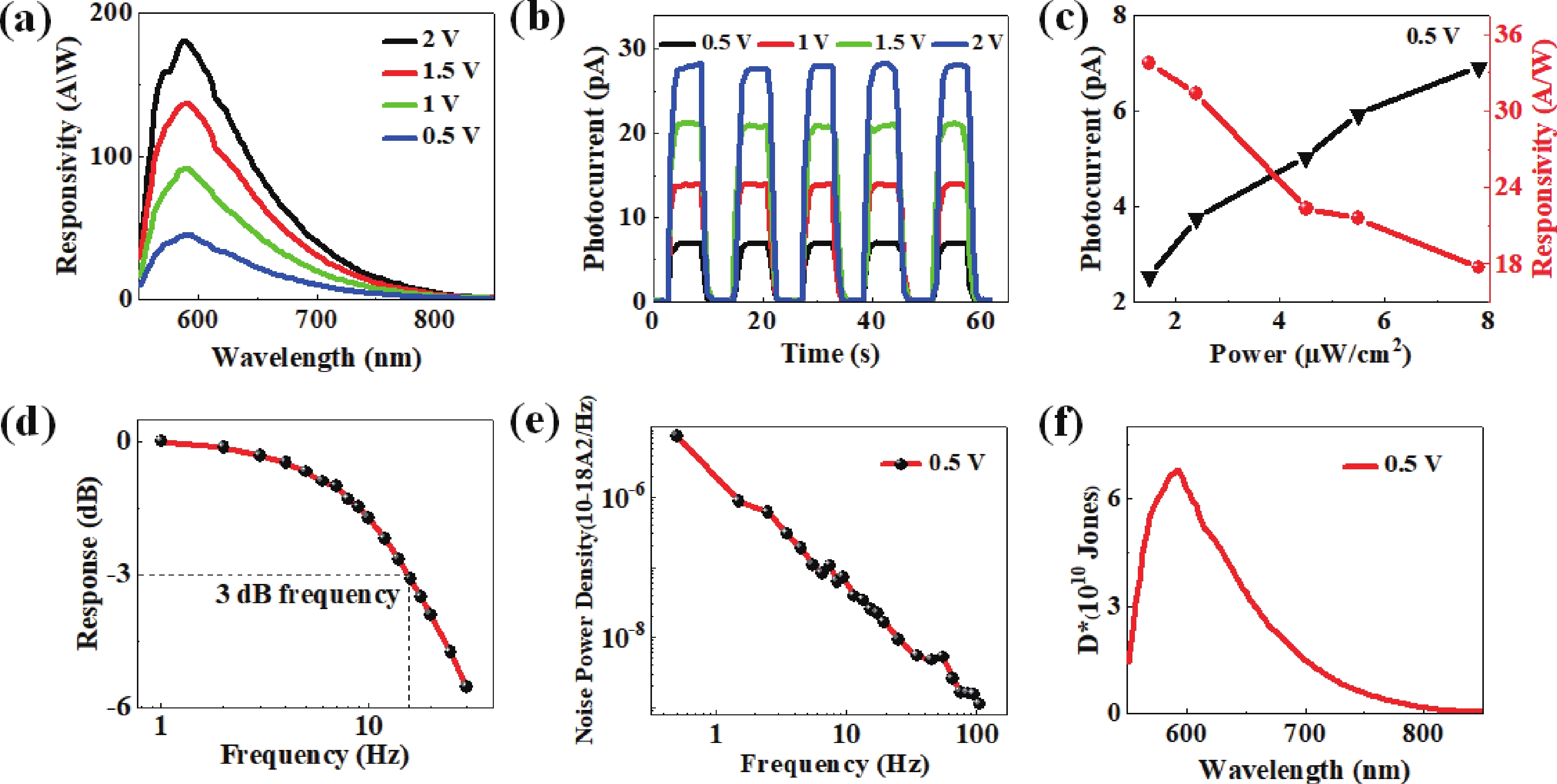
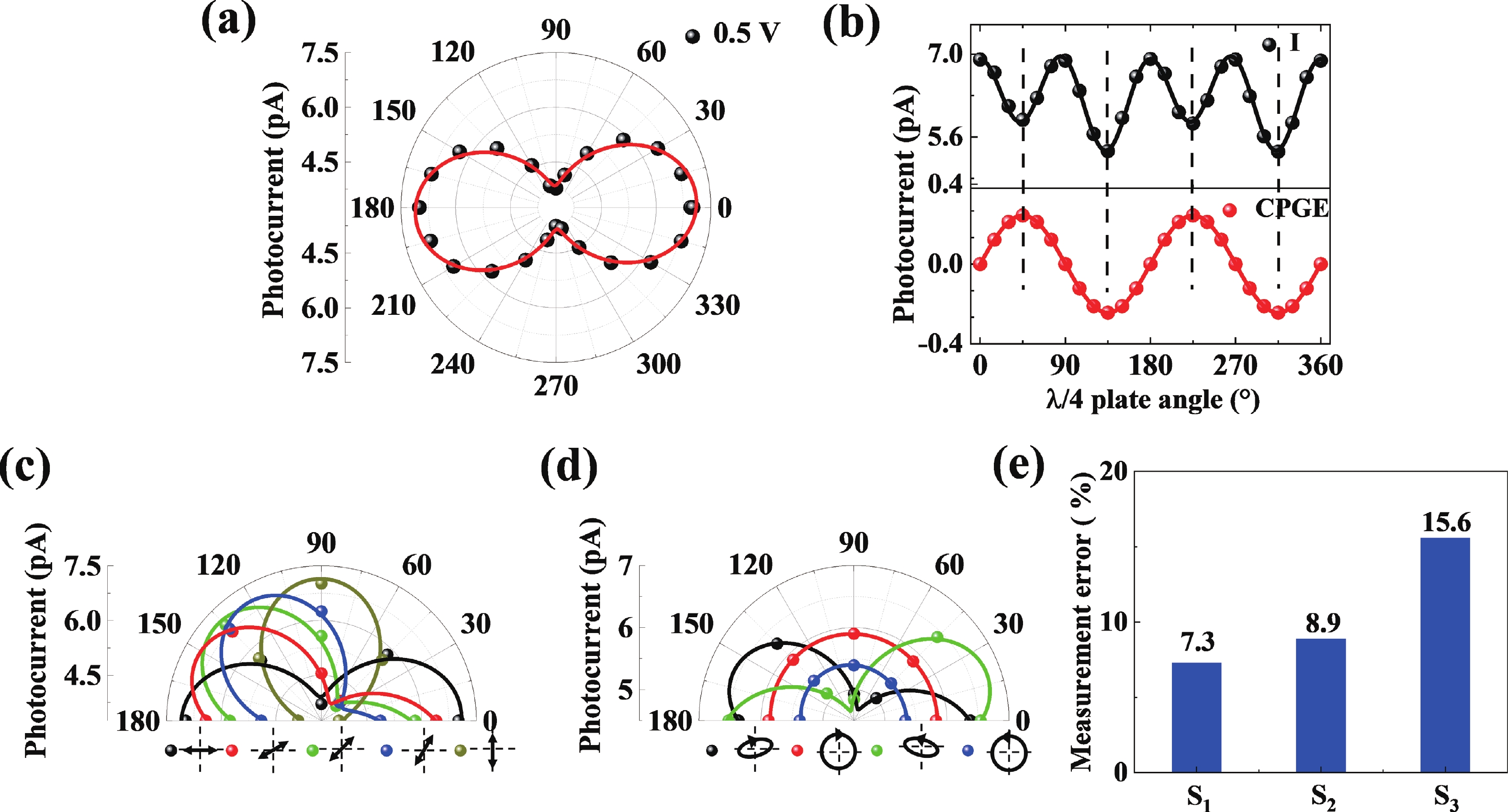
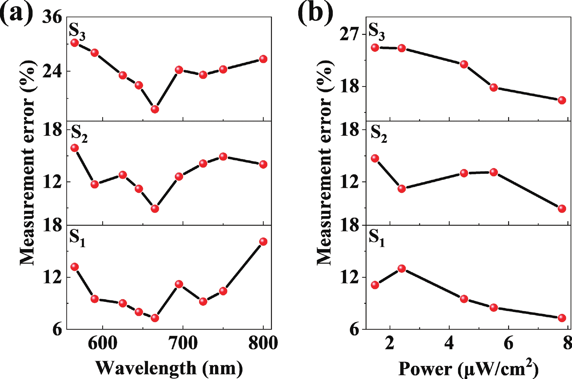
Full-Stokes polarimeters can detect the polarization states of light, which is critical for the next-generation optical and optoelectronic systems. Traditional full-Stokes polarimeters are either based on bulky optical systems or complex metasurface structures, which cause the system complexity with unessential energy loss. Recently, filterless on-chip full-Stokes polarimeters have been demonstrated by using optical anisotropic materials which are able to detect the circularly polarized light. Nevertheless, those on-chip full-Stokes polarimeters have either the limited detection wavelength range or relatively poor device performance that need to be further improved. Here, we report the high performance broadband full-Stokes polarimeters based on rhenium disulfide (ReS2). While the anisotropic structure of the ReS2 introduces the in-plane optical anisotropy for linearly polarized light (LP) detection, Schottky contacts formed by the ReS2−Au could break the symmetry, which can detect circularly polarized (CP) light. By building a proper model, all four Stokes parameters can be extracted by using the ReS2 nanobelt device. The device delivers a photoresponsivity of 181 A/W, a detectivity of 6.8 × 10¹⁰ Jones and can sense the four Stokes parameters of incident light within a wide range of wavelength from 565−800 nm with reasonable average errors. We believe our study provides an alternative strategy to develop high performance broadband on-chip full-Stokes polarimeters.