Issue Browser
Volume 46, Issue 4,
Apr 2025
J. Semicond.
2025, 46(4): 041101 doi: 10.1088/1674-4926/24100016
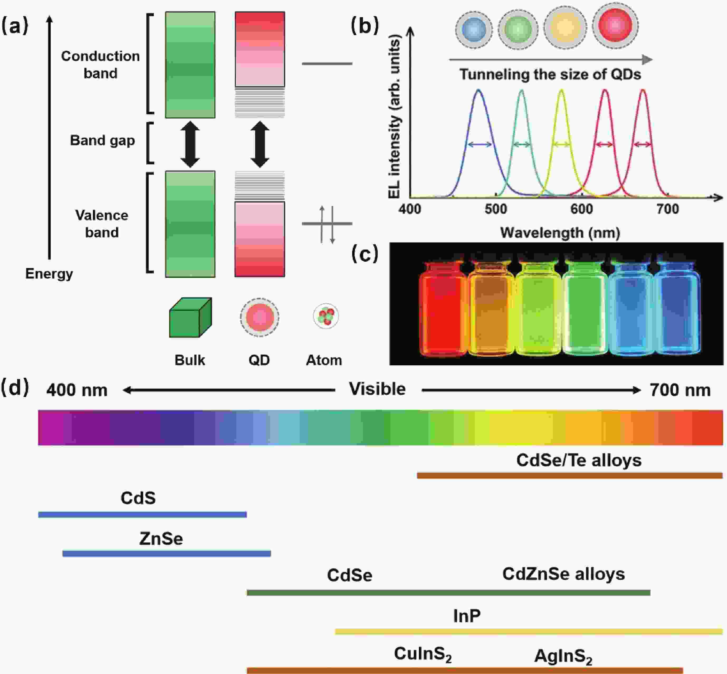
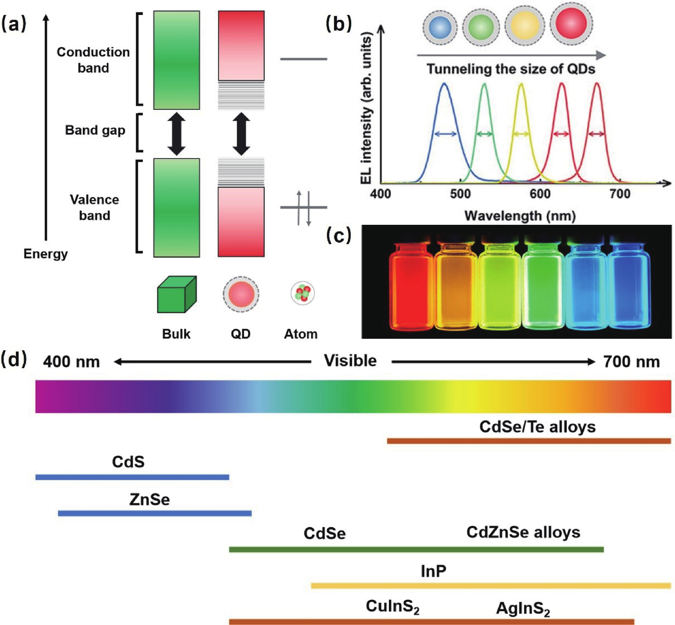
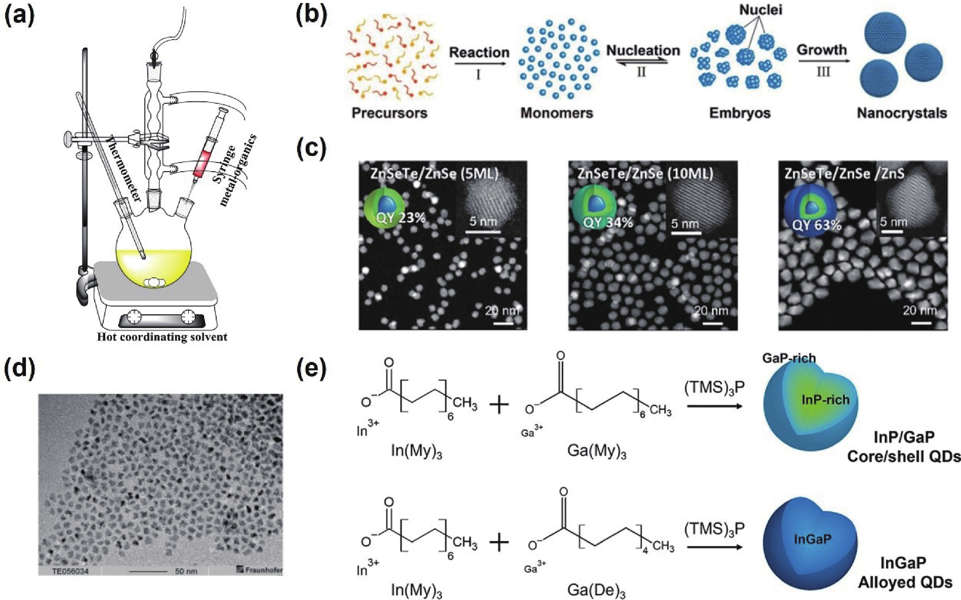
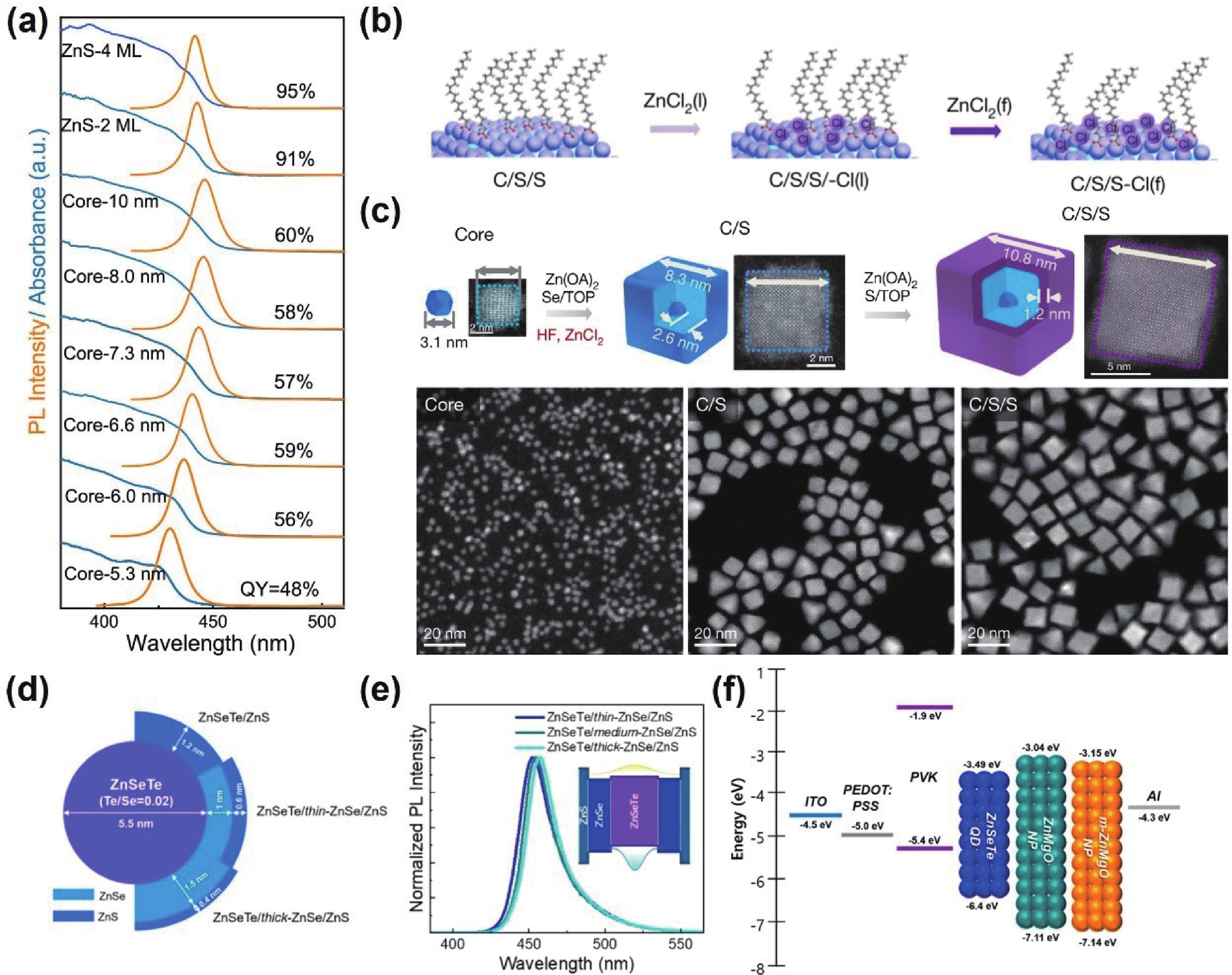
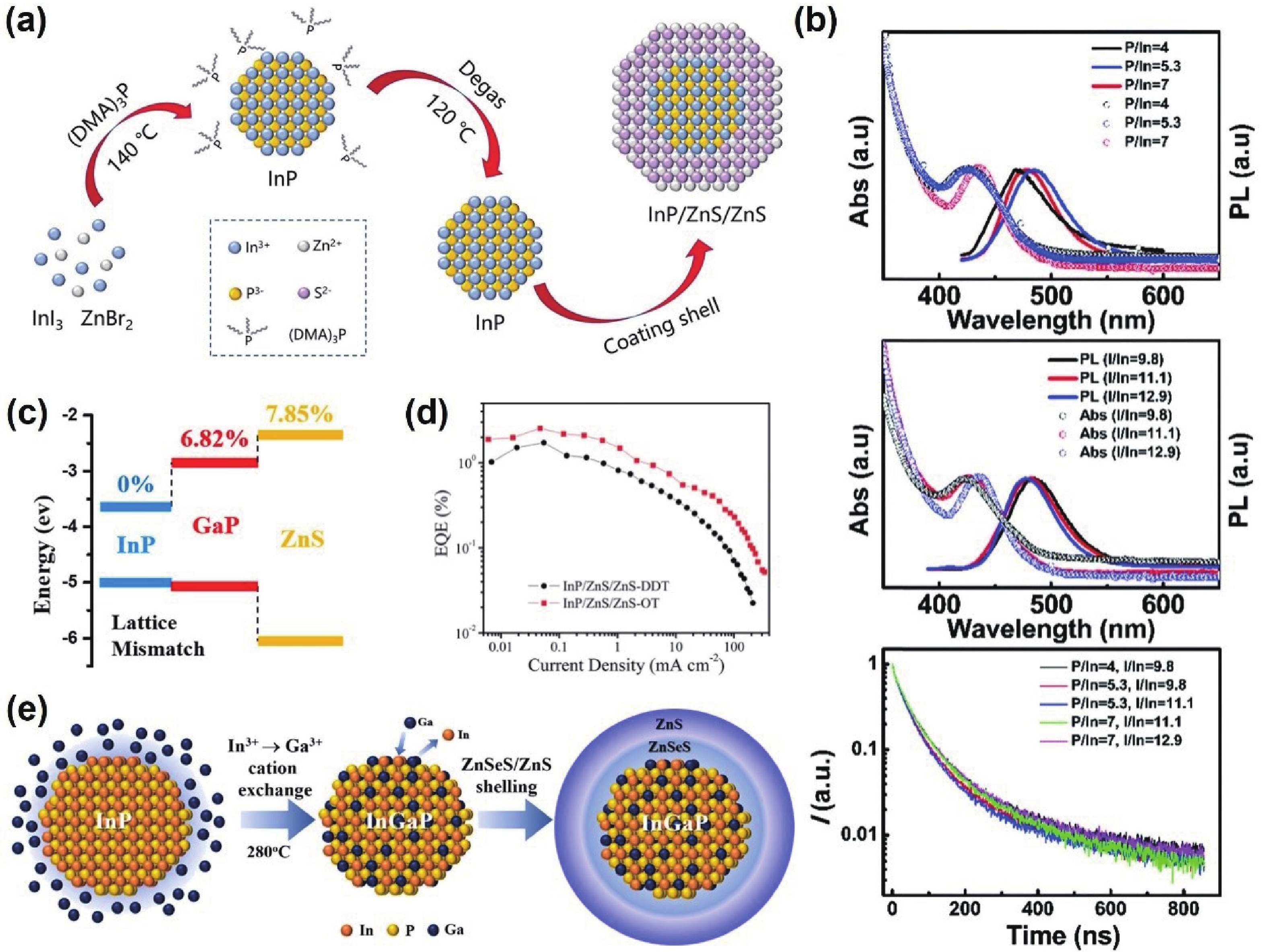
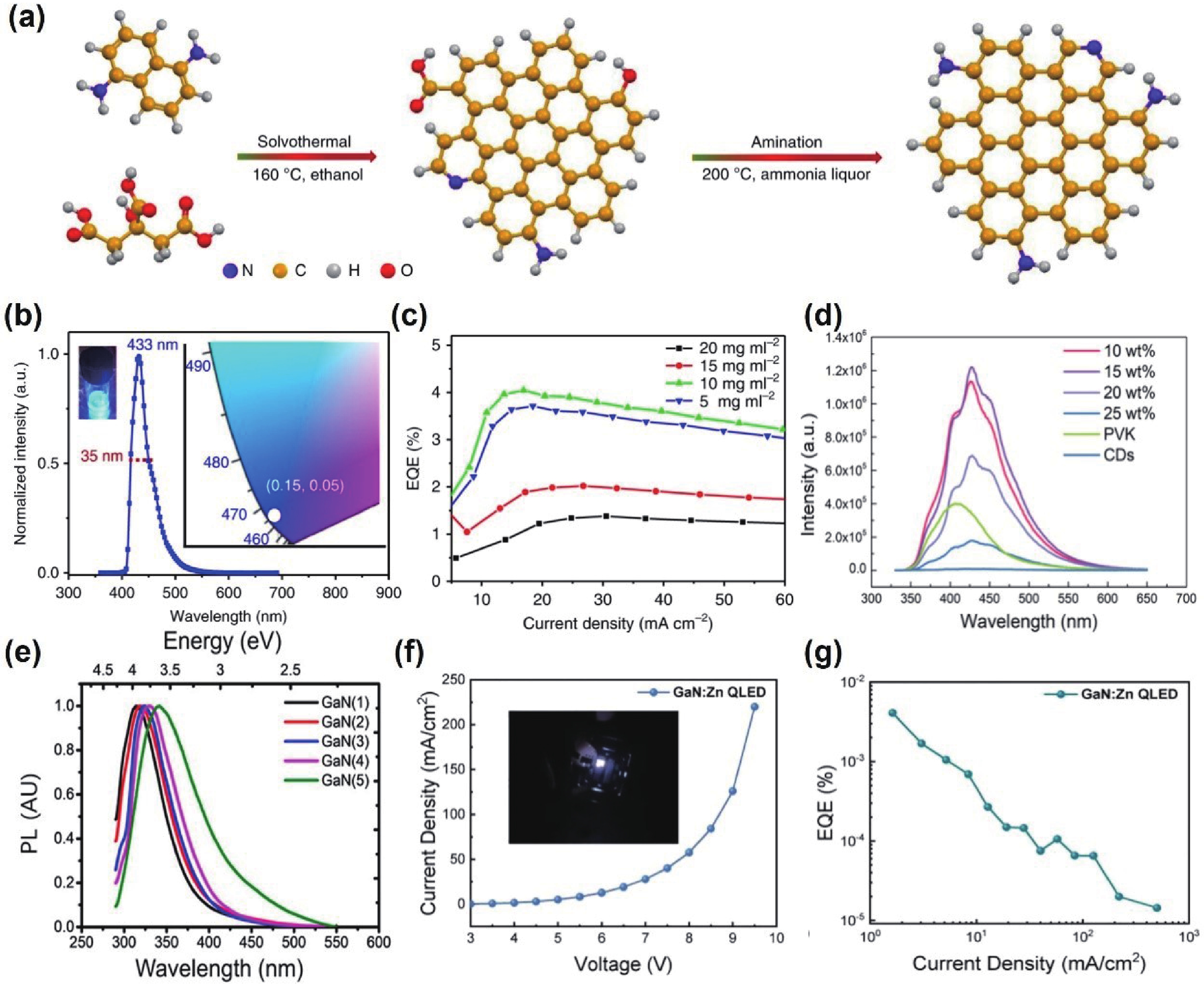
Colloidal quantum dots (CQDs) are highly regarded for their outstanding photovoltaic characteristics, including excellent color purity, stability, high photoluminescence quantum yield (PLQY), narrow emission spectra, and ease of solution processing. Despite significant progress in quantum dot light-emitting diodes (QLEDs) technology since its inception in 1994, blue QLEDs still fall short in efficiency and lifespan compared to red and green versions. The toxicity concerns associated with Cd/Pb-based quantum dots (QDs) have spurred the development of heavy-metal-free alternatives, such as group Ⅱ−Ⅵ (e.g., ZnSe-based QDs), group Ⅲ−Ⅴ (e.g., InP, GaN QDs), and carbon dots (CDs). In this review, we discuss the key properties and development history of quantum dots (QDs), various synthesis approaches, the role of surface ligands, and important considerations in developing core/shell (C/S) structured QDs. Additionally, we provide an outlook on the challenges and future directions for blue QLEDs.
J. Semicond.
2025, 46(4): 042101 doi: 10.1088/1674-4926/24050026
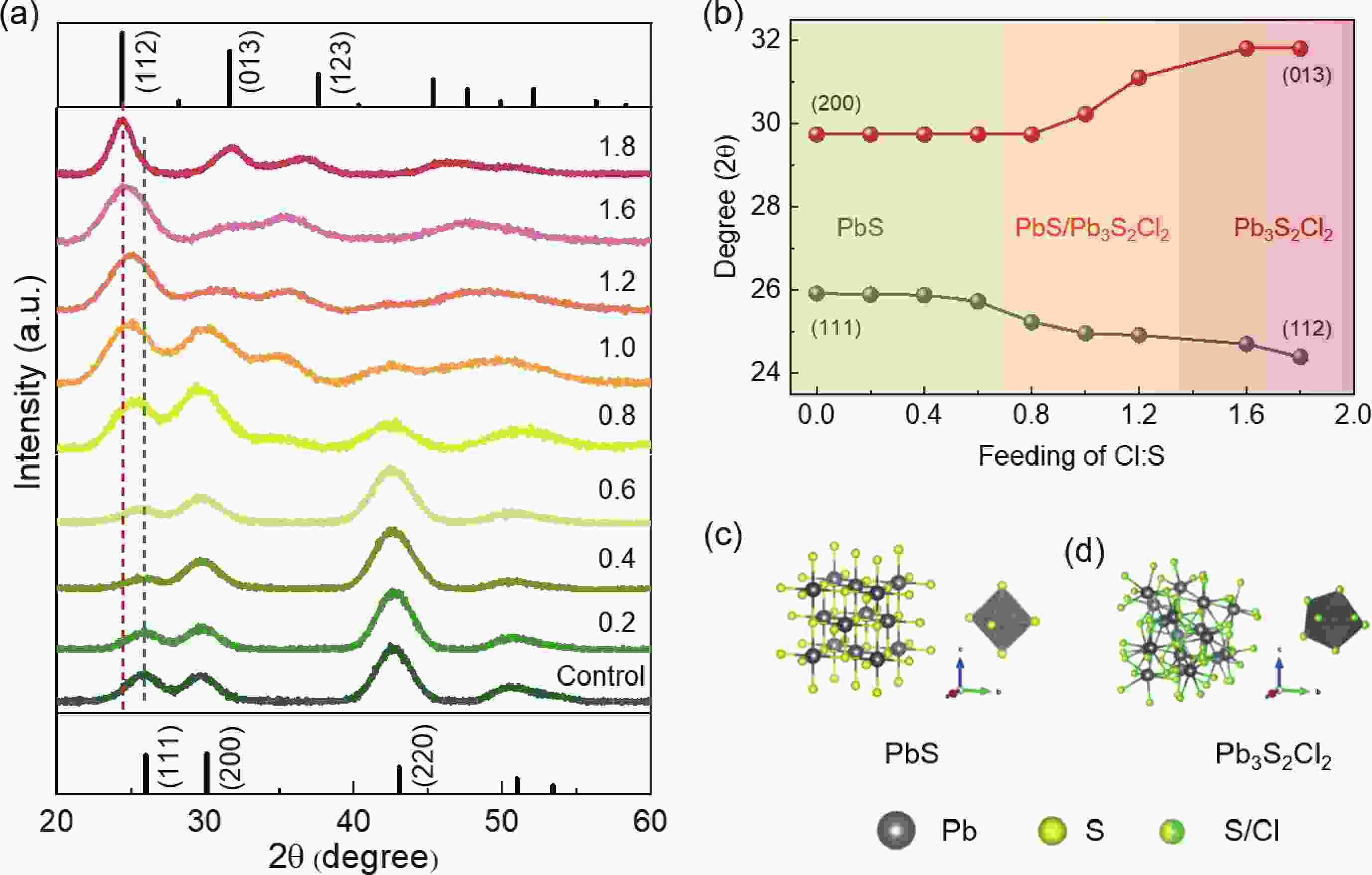
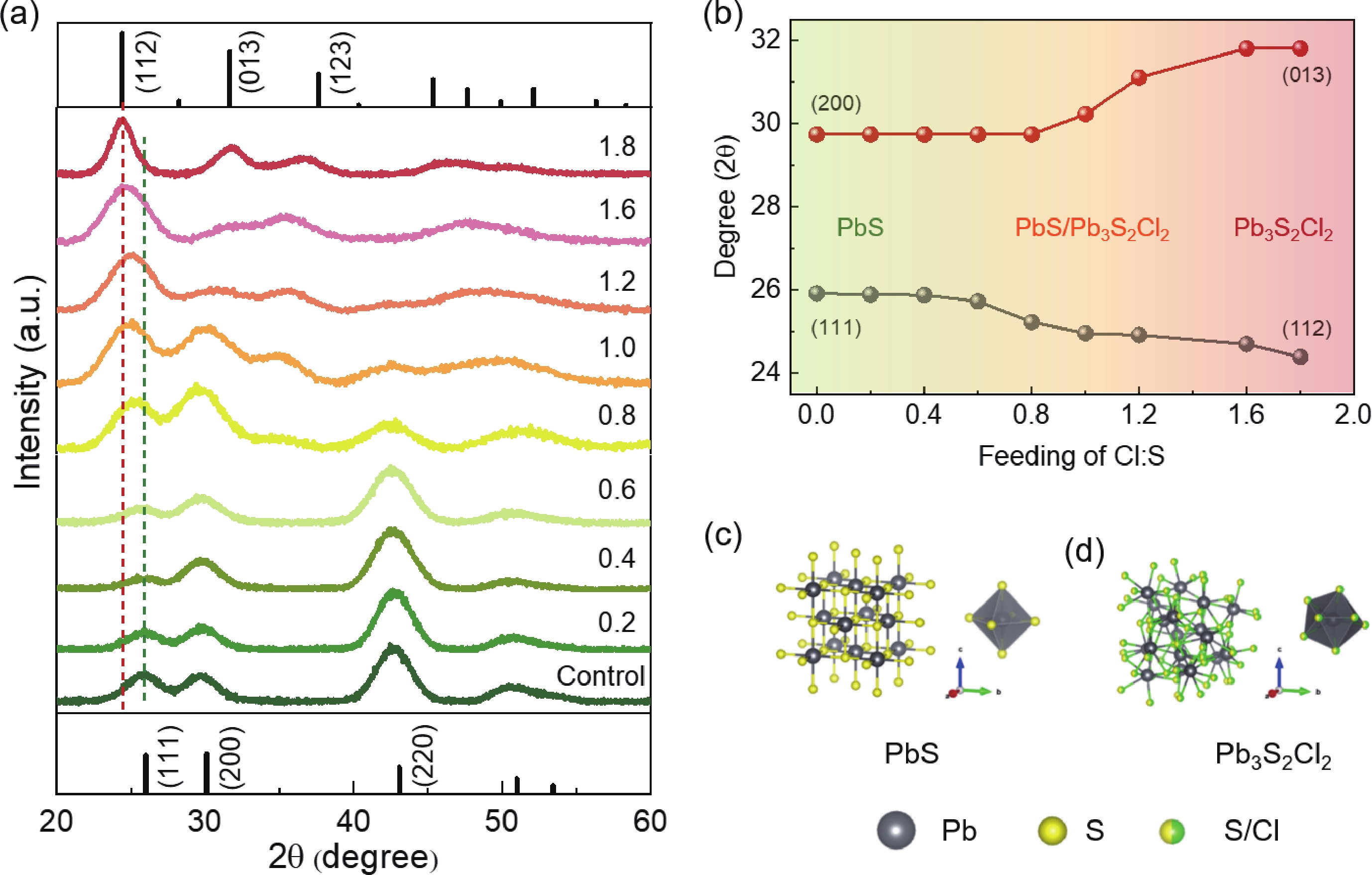
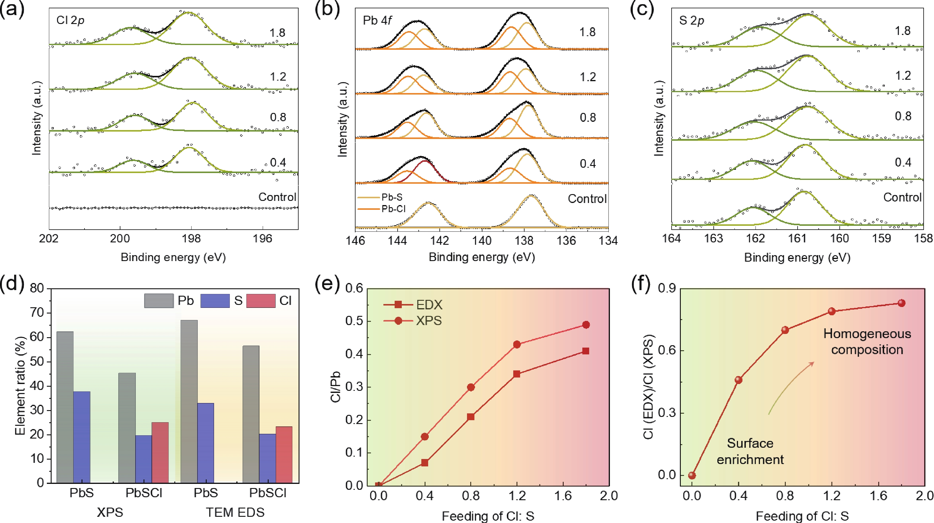
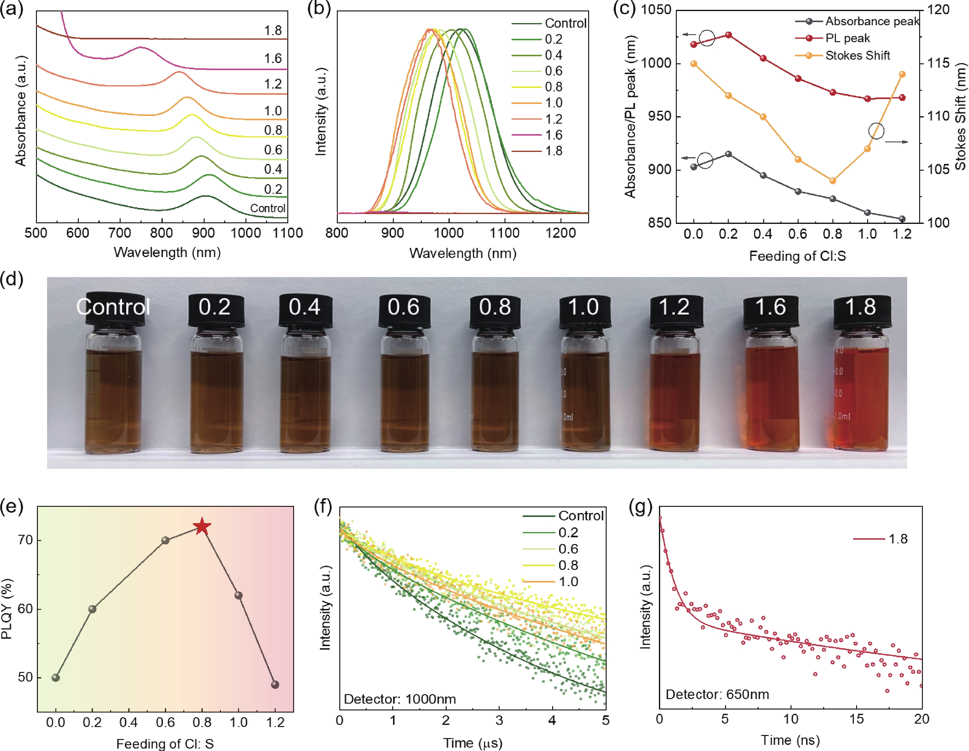
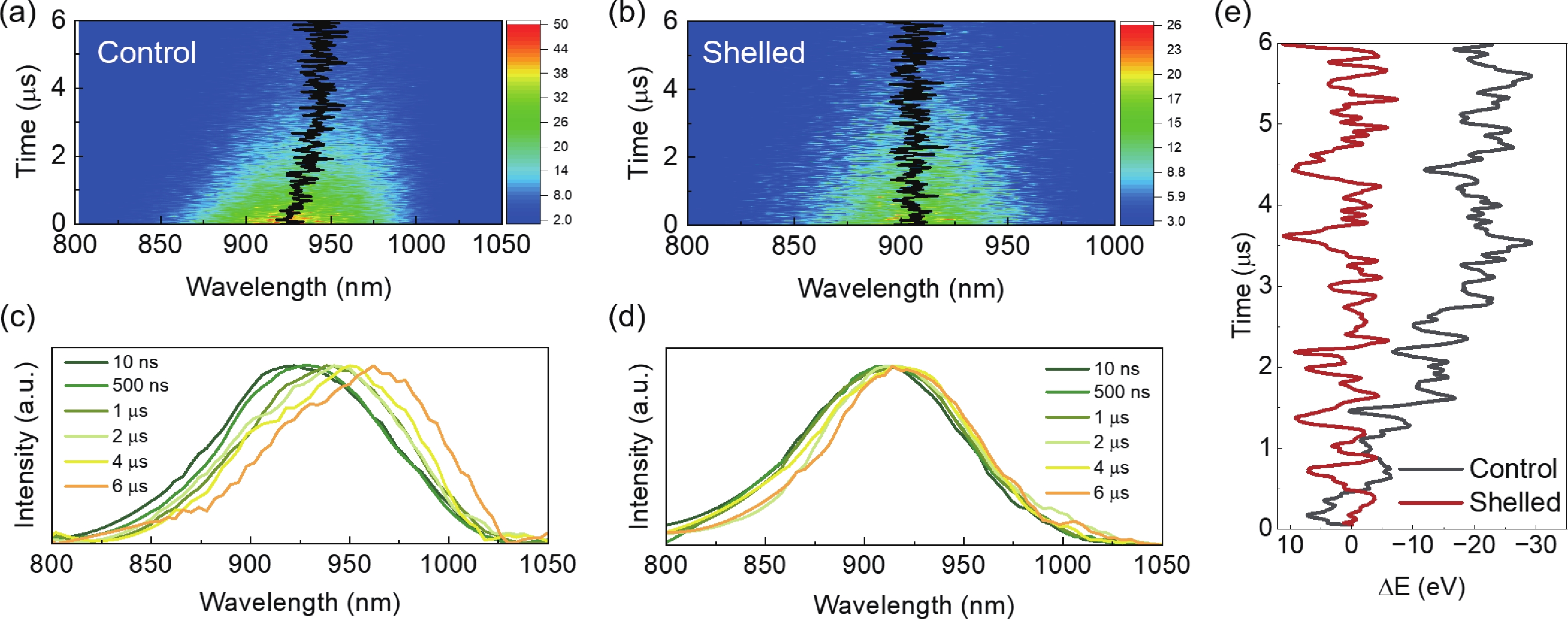
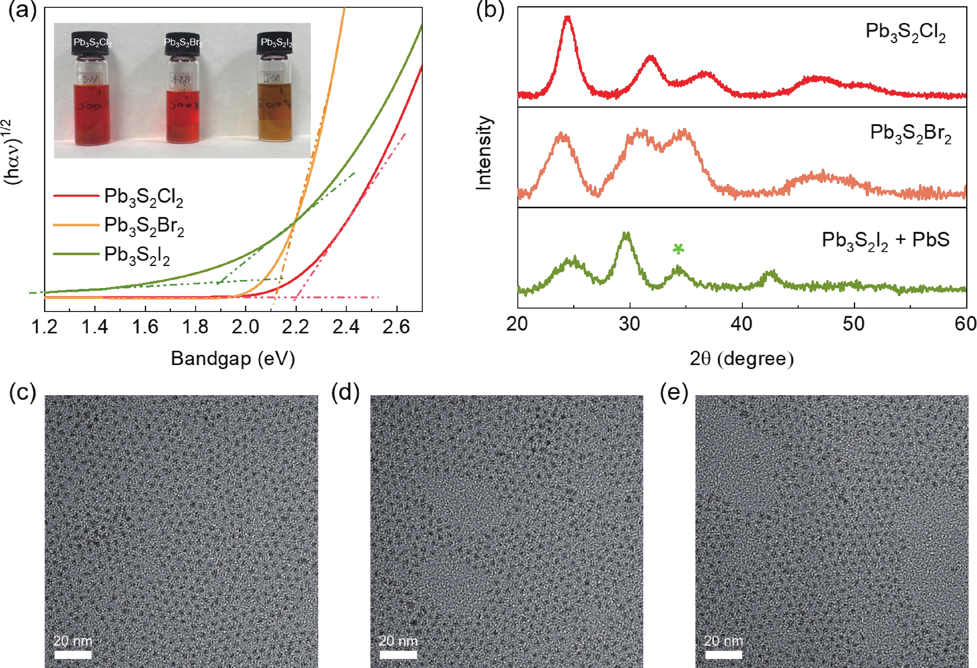
Lead chalcohalides (PbYX, X = Cl, Br, I; Y = S, Se) is an extension of the classic Pb chalcogenides (PbY). Constructing the heterogeneous integration with PbYX and PbY material systems makes it possible to achieve significantly improved optoelectronic performance. In this work, we studied the effect of introducing halogen precursors on the structure of classical PbS nanocrystals (NCs) during the synthesis process and realized the preparation of PbS/Pb3S2X2 core/shell structure for the first time. The core/shell structure can effectively improve their optical properties. Furthermore, our approach enables the synthesis of Pb3S2Br2 that had not yet been reported. Our results not only provide valuable insights into the heterogeneous integration of PbYX and PbY materials to elevate material properties but also provide an effective method for further expanding the preparation of PbYX material systems.
J. Semicond.
2025, 46(4): 042102 doi: 10.1088/1674-4926/24100011
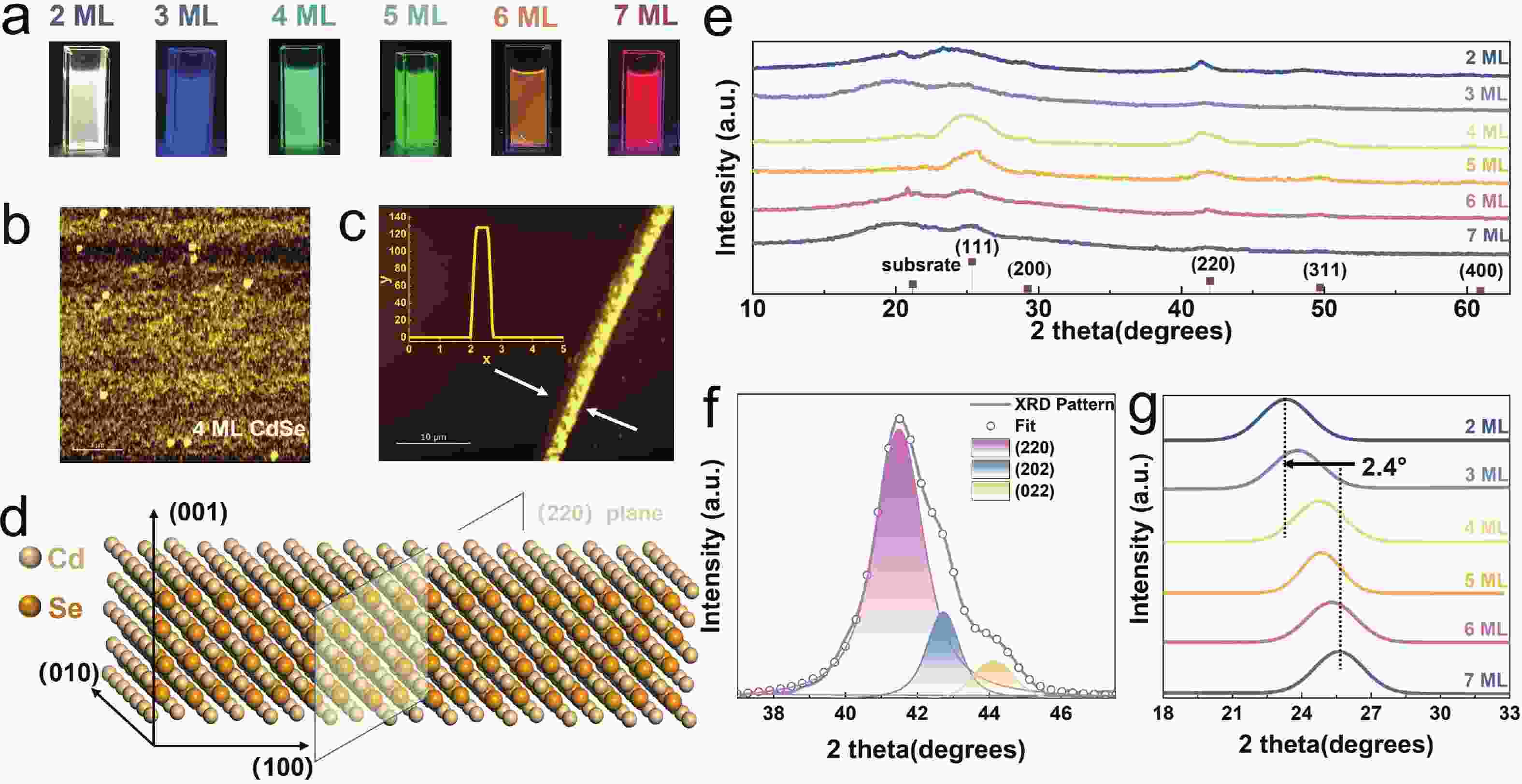
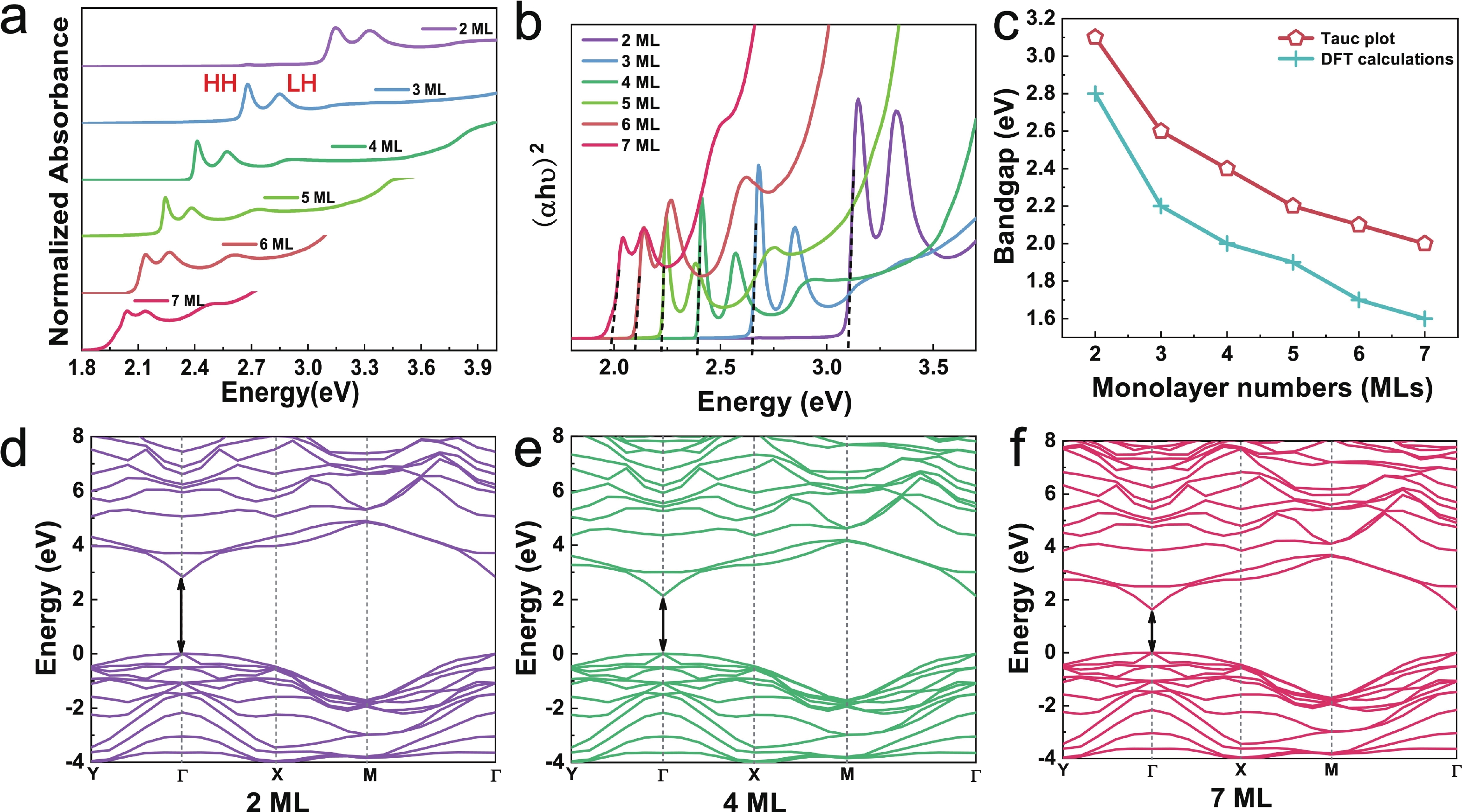
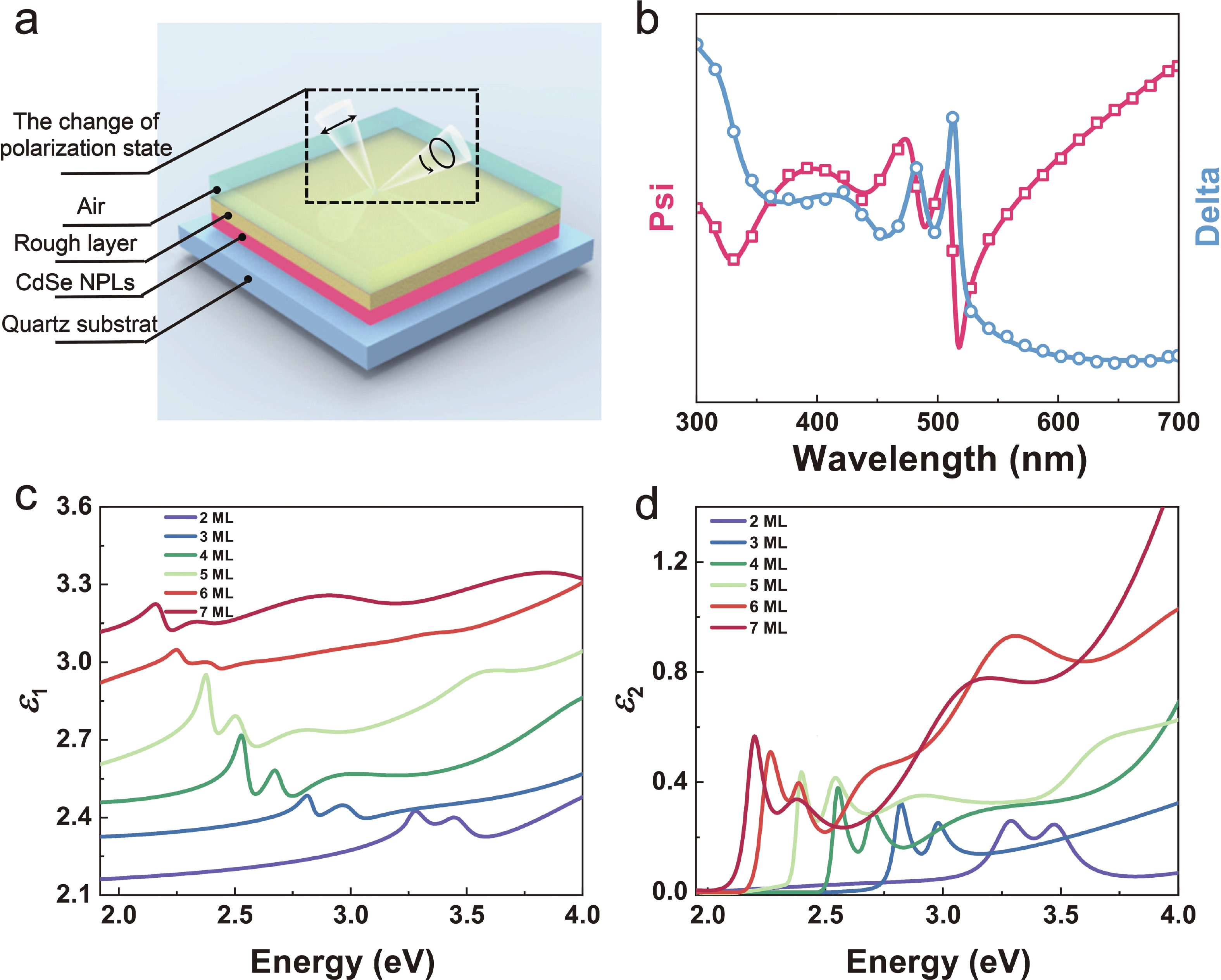
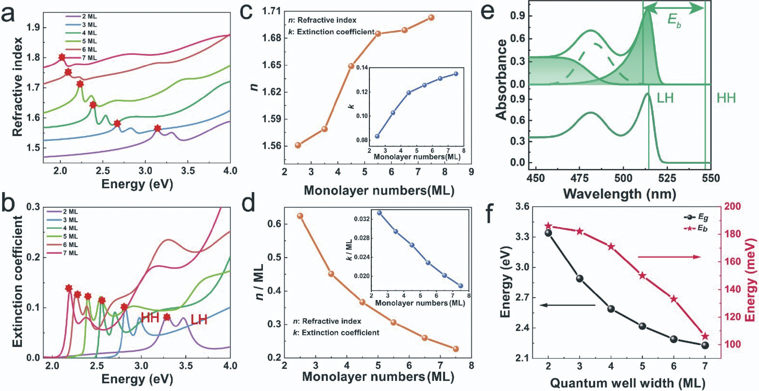
Semiconductor colloidal quantum wells (CQWs) with atomic-precision layer thickness are rapidly gaining attention for next-generation optoelectronic applications due to their tunable optical and electronic properties. In this study, we investigate the dielectric and optical characteristics of CdSe CQWs with monolayer numbers ranging from 2 to 7, synthesized via thermal injection and atomic layer (c-ALD) deposition techniques. Through a combination of spectroscopic ellipsometry (SE) and first-principles calculations, we demonstrate the significant tunability of the bandgap, refractive index, and extinction coefficient, driven by quantum confinement effects. Our results show a decrease in bandgap from 3.1 to 2.0 eV as the layer thickness increases. Furthermore, by employing a detailed analysis of the absorption spectra, accounting for exciton localization and asymmetric broadening, we precisely capture the relationship between monolayer number and exciton binding energy. These findings offer crucial insights for optimizing CdSe CQWs in optoelectronic device design by leveraging their layer-dependent properties.
J. Semicond.
2025, 46(4): 042103 doi: 10.1088/1674-4926/24120018
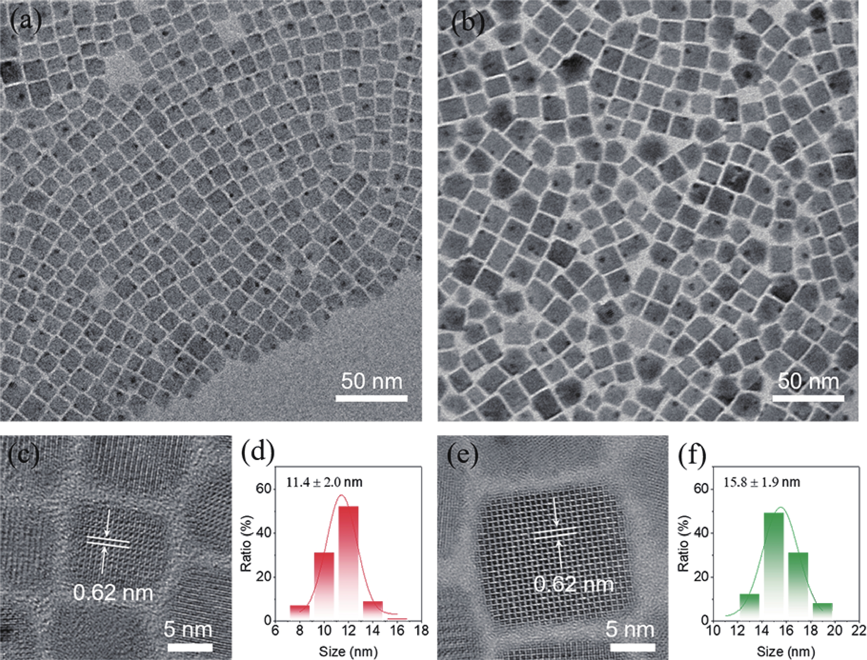
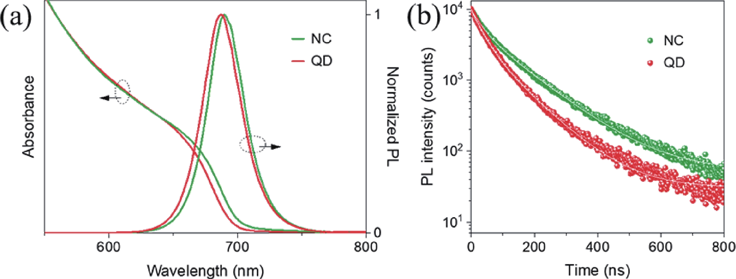
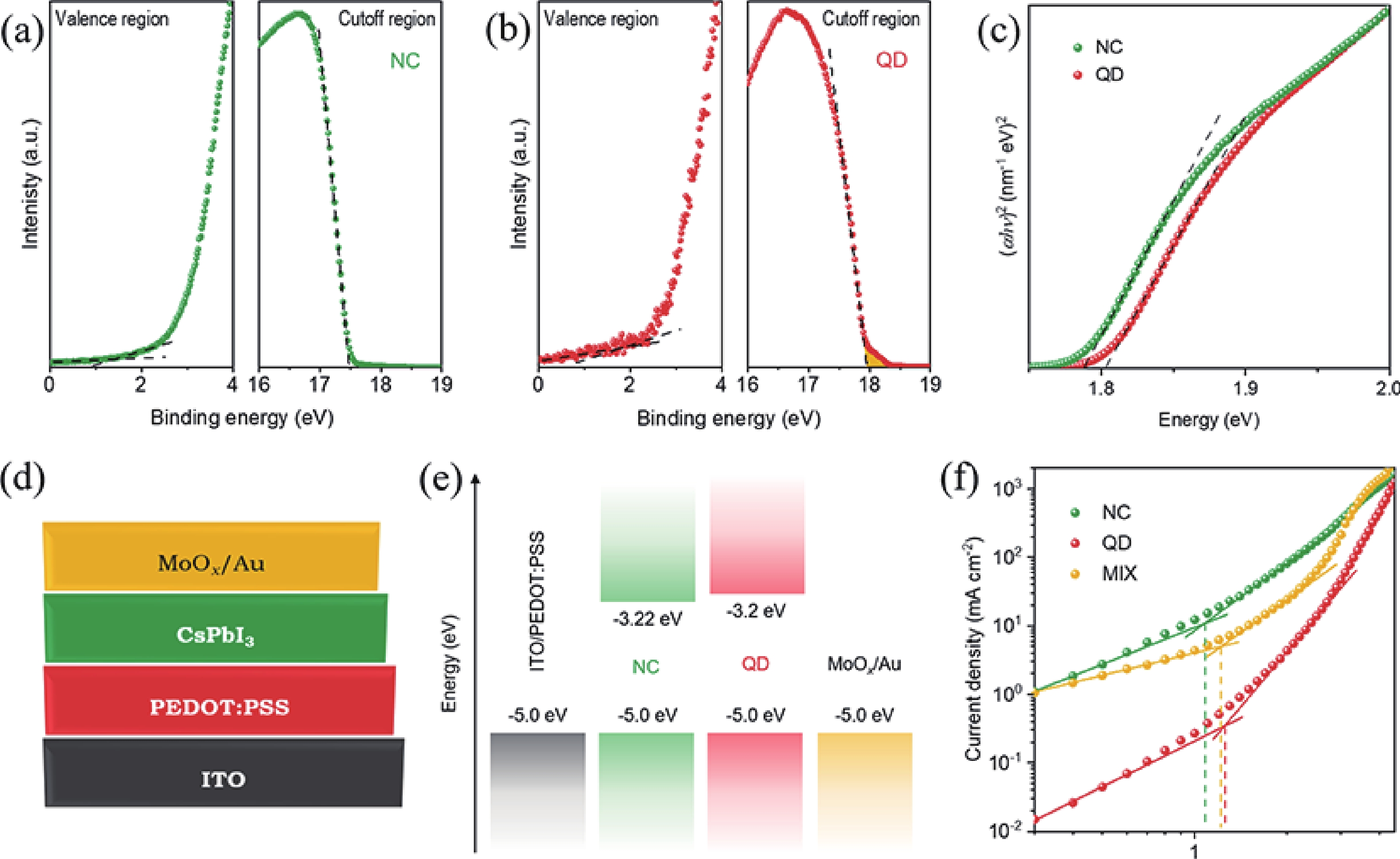
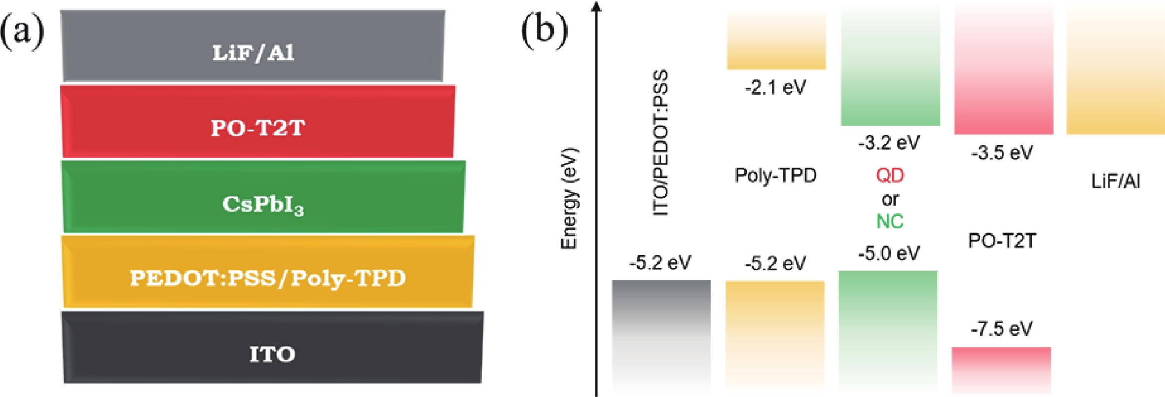
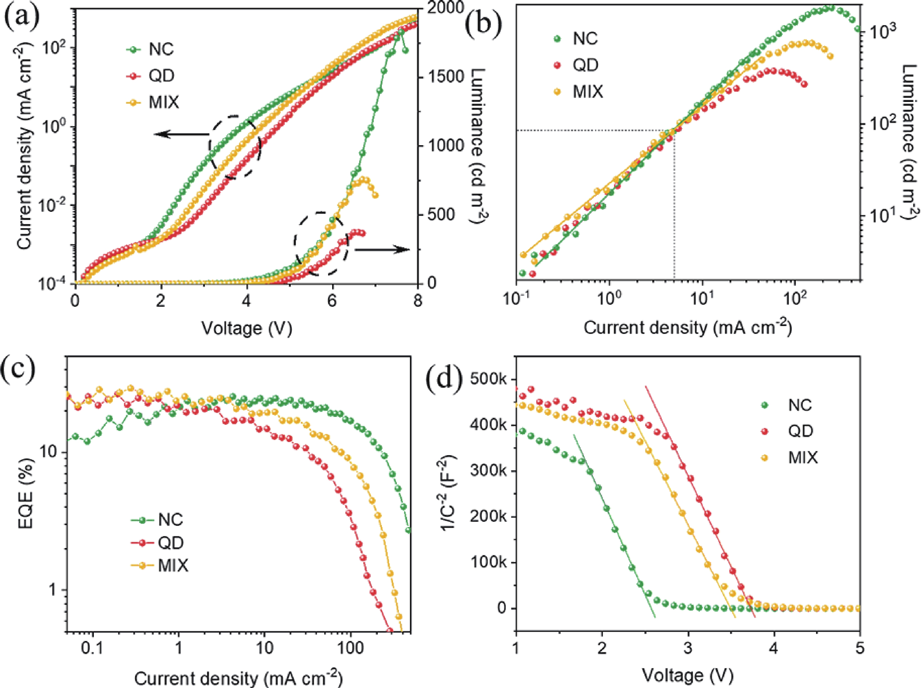
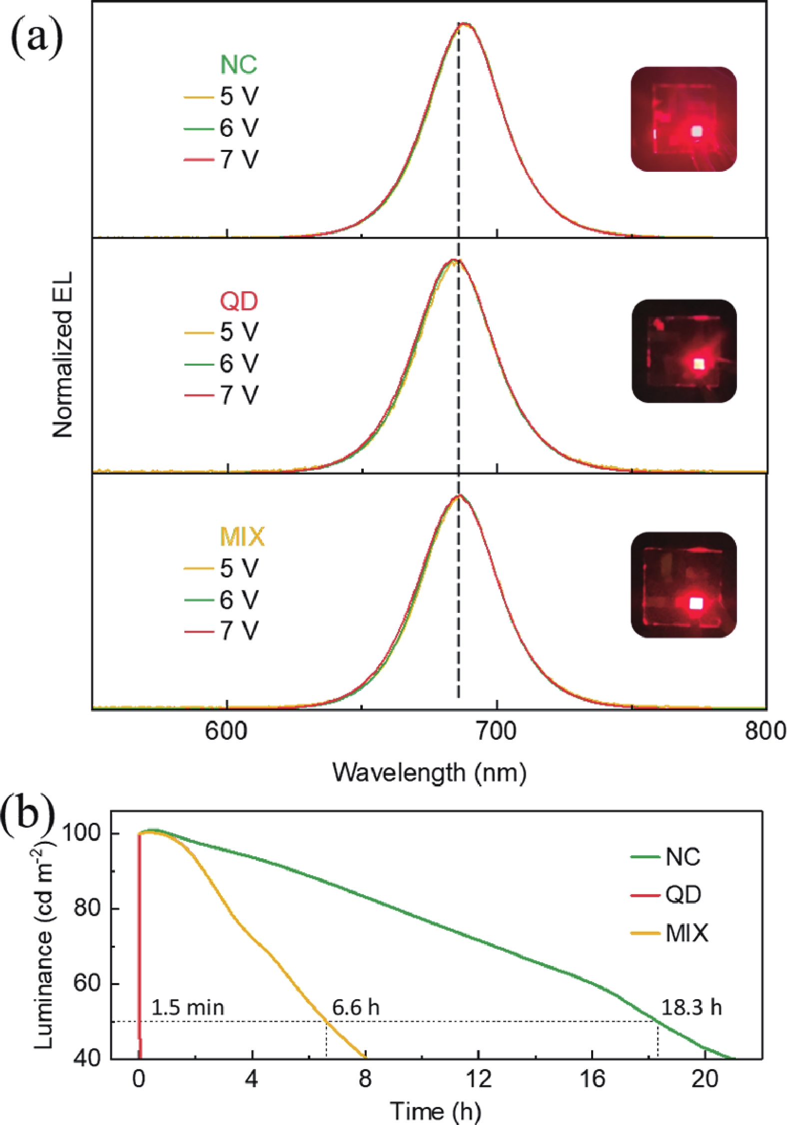
The quantum confinement effect fundamentally alters the optical and electronic properties of quantum dots (QDs), making them versatile building blocks for next-generation light-emitting diodes (LEDs). This study investigates how quantum confinement governs the charge transport, exciton dynamics, and emission efficiency in QD-LEDs, using CsPbI3 QDs as a model system. By systematically varying QD sizes, we reveal size-dependent trade-offs in LED performance, such as enhanced efficiency for smaller QDs but increased brightness and stability for larger QDs under high current densities. Our findings offer critical insights into the design of high-performance QD-LEDs, paving the way for scalable and energy-efficient optoelectronic devices.
J. Semicond.
2025, 46(4): 042104 doi: 10.1088/1674-4926/25030003
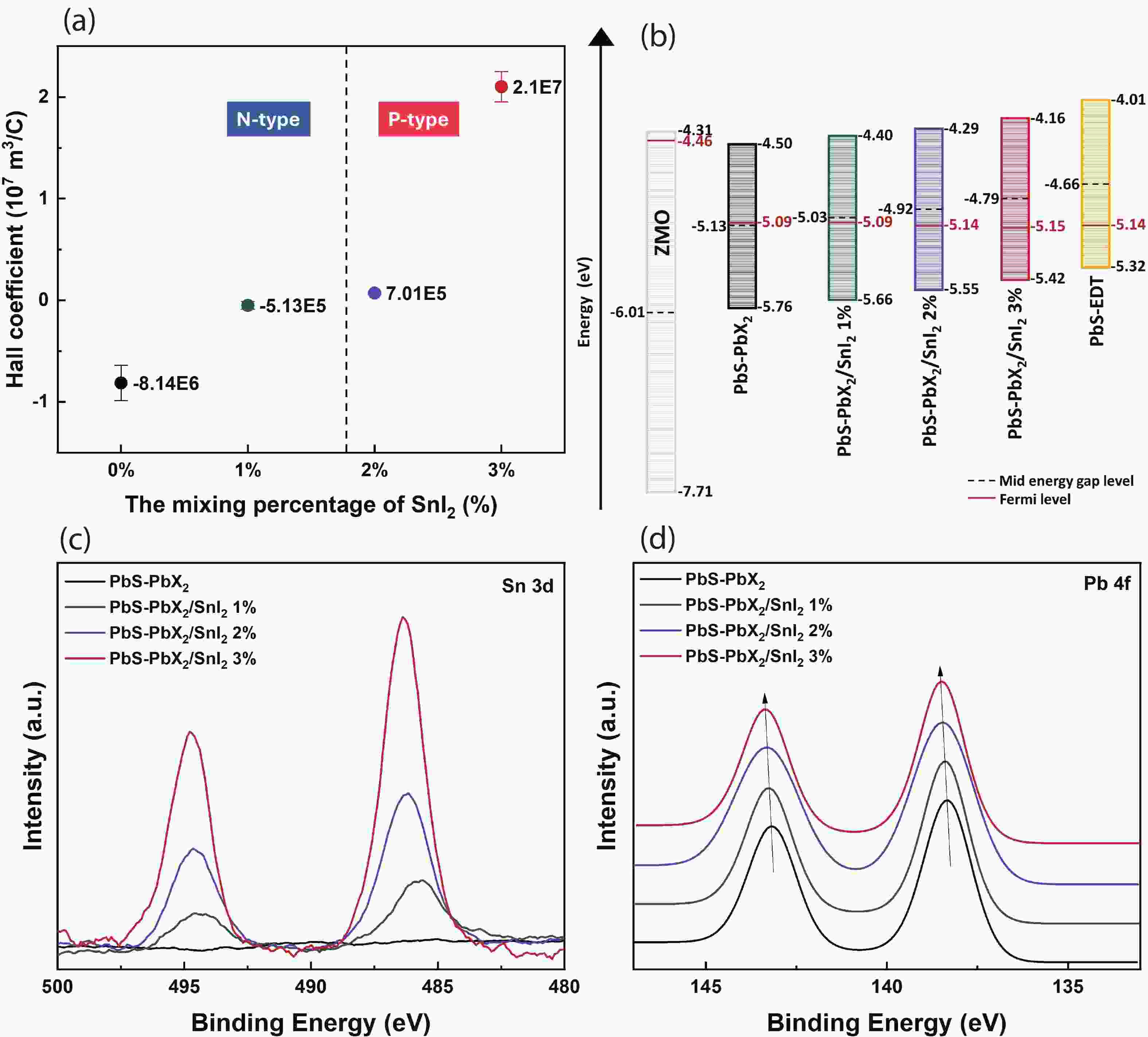
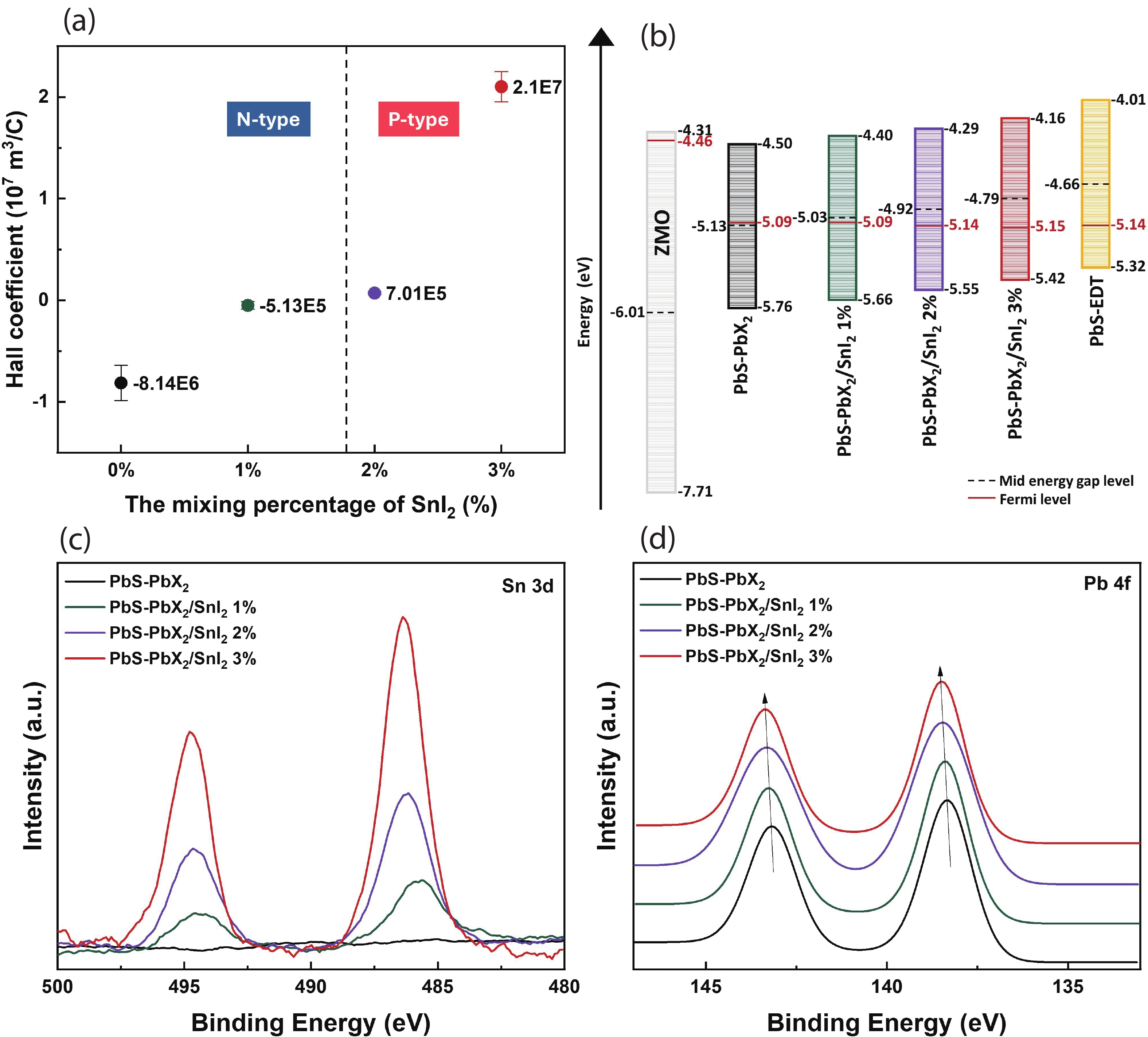
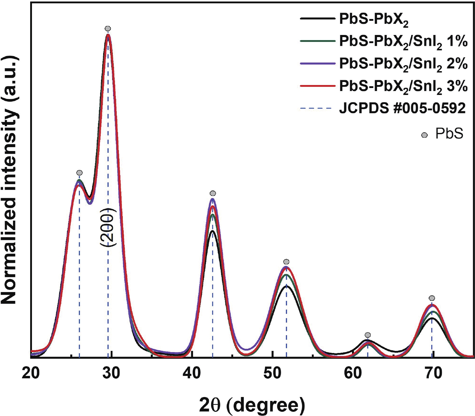
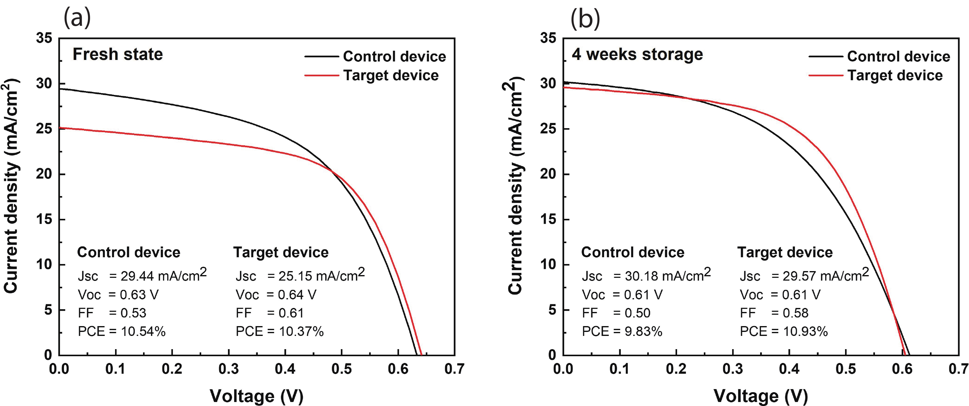
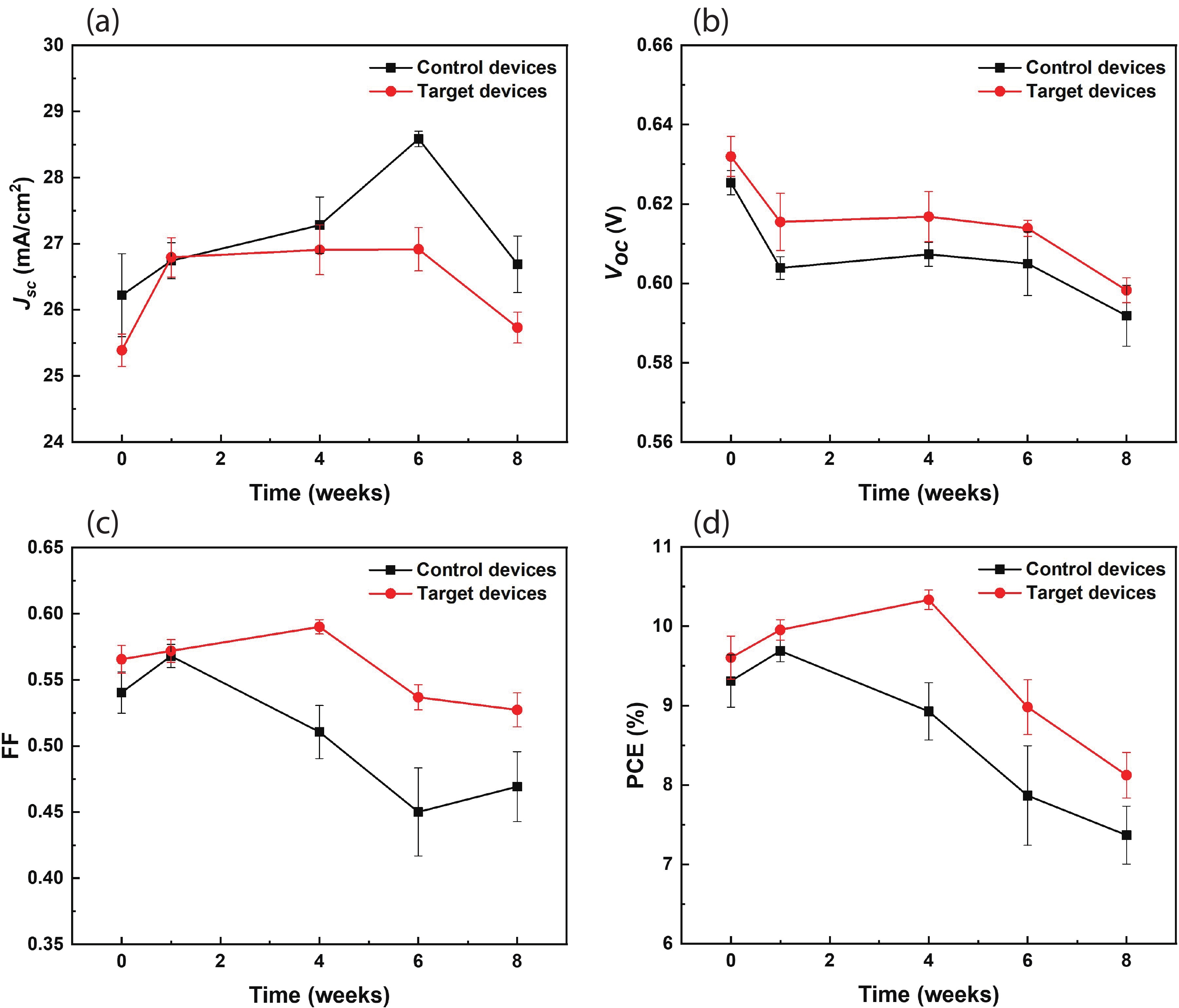
Traditional p-type colloidal quantum dot (CQD) hole transport layers (HTLs) used in CQD solar cells (CQDSCs) are commonly based on organic ligands exchange and the layer-by-layer (LbL) technique. Nonetheless, the ligand detachment and complex fabrication process introduce surface defects, compromising device stability and efficiency. In this work, we propose a solution-phase ligand exchange (SPLE) method utilizing inorganic ligands to develop stable p-type lead sulfide (PbS) CQD inks for the first time. Various amounts of tin (II) iodide (SnI2) were mixed with lead halide (PbX2; X = I, Br) in the ligand solution. By precisely controlling the SnI₂ concentration, we regulate the transition of PbS QDs from n-type to p-type. PbS CQDSCs were fabricated using two different HTL approaches: one with 1,2-ethanedithiol (EDT)-passivated QDs via the LbL method (control) and another with inorganic ligand-passivated QD ink (target). The target devices achieved a higher power conversion efficiency (PCE) of 10.93%, compared to 9.83% for the control devices. This improvement is attributed to reduced interfacial defects and enhanced carrier mobility. The proposed technique offers an efficient pathway for producing stable p-type PbS CQD inks using inorganic ligands, paving the way for high-performance and flexible CQD-based optoelectronic devices.
J. Semicond.
2025, 46(4): 041401 doi: 10.1088/1674-4926/24100029

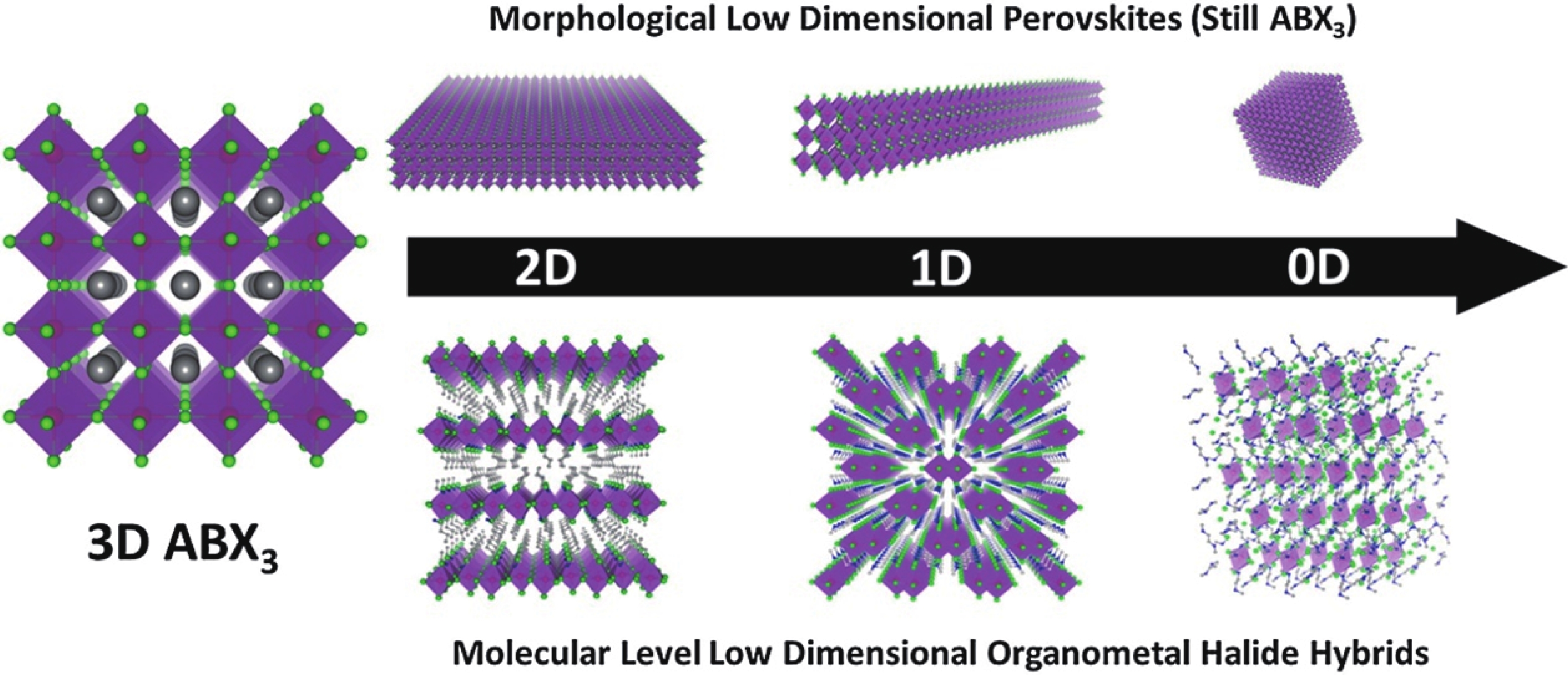
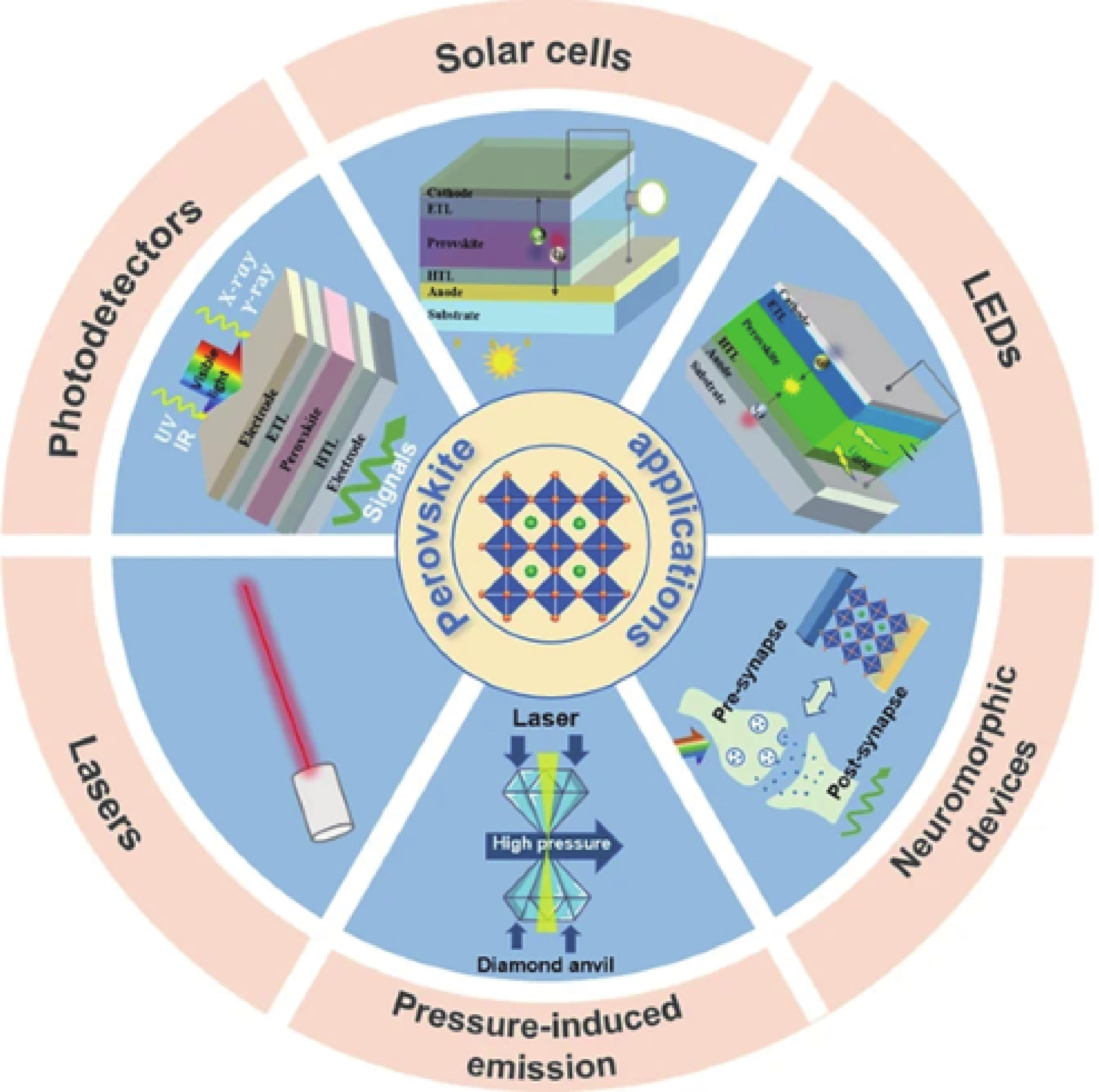
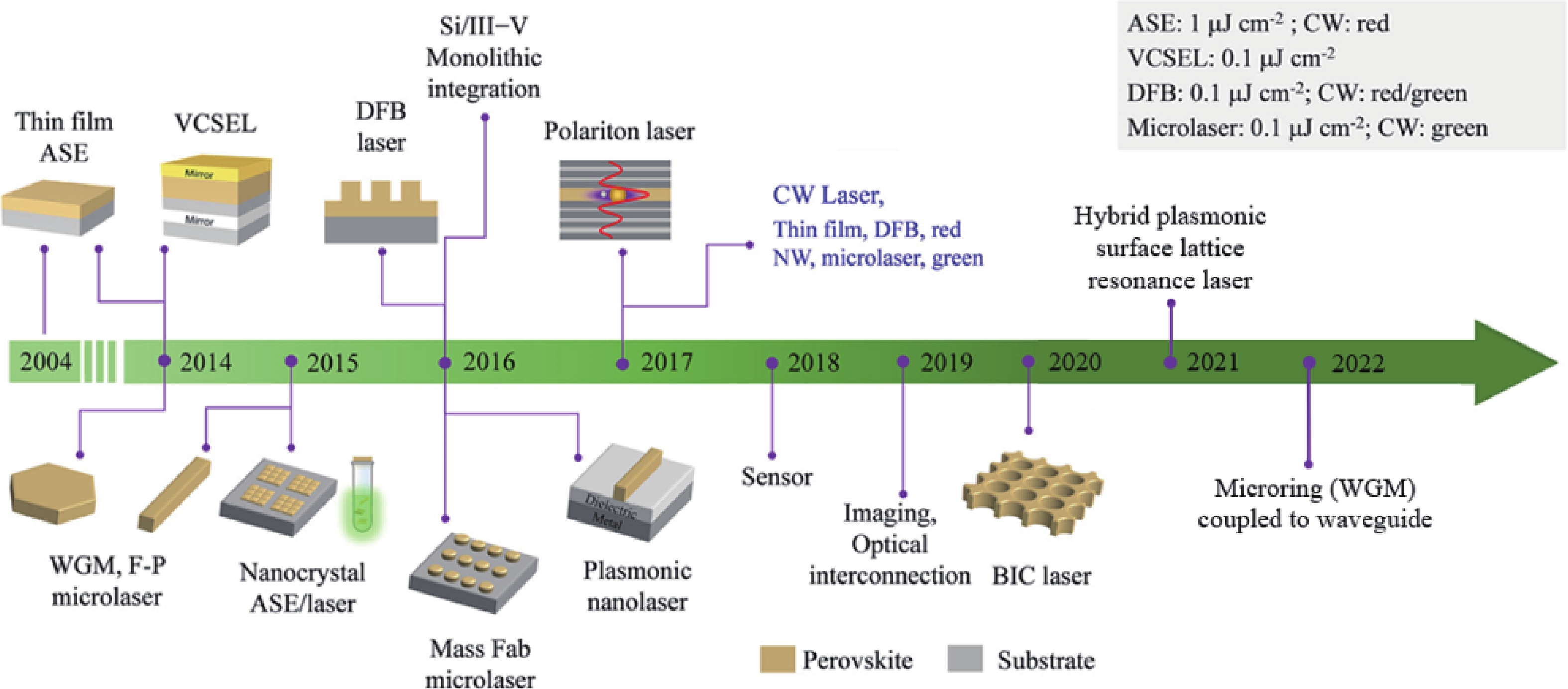
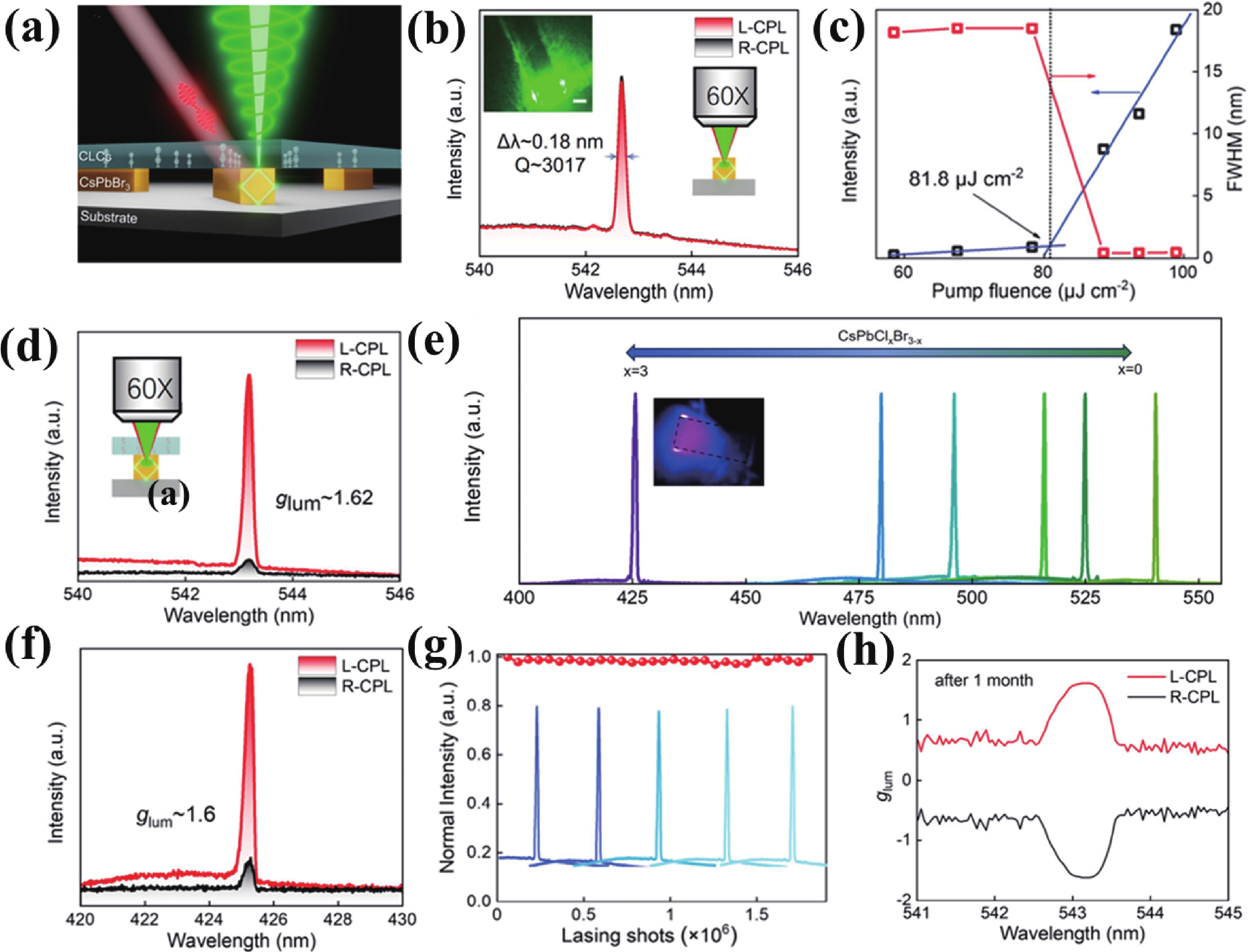
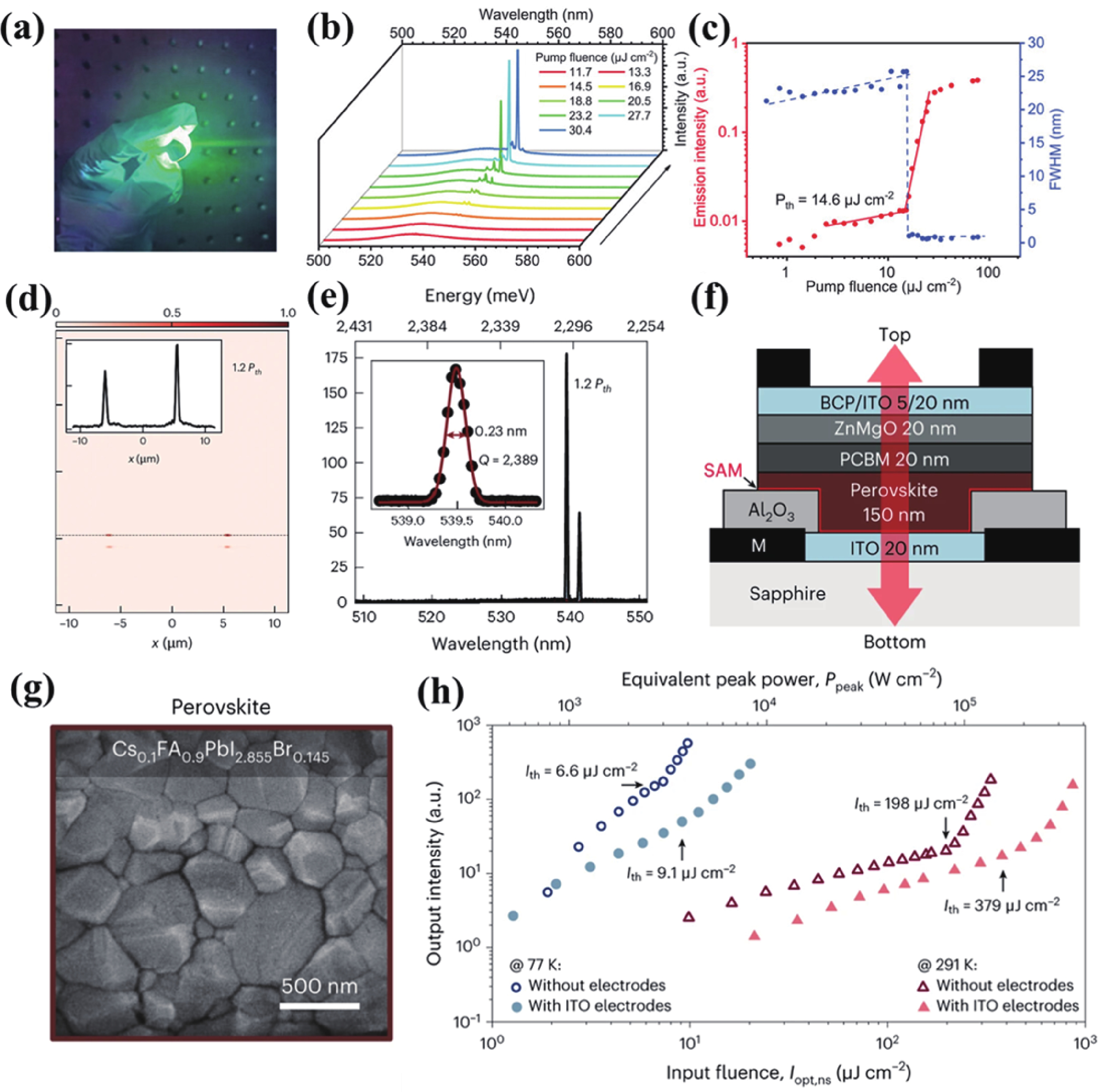
Perovskite materials have emerged as promising candidates for various optoelectronic applications owing to their remarkable optoelectronic properties and easy solution processing. Metal halide perovskites, as direct-bandgap semiconductors, show an excellent class of optical gain media, which makes them applicable to the development of low-threshold or even thresholdless lasers. This mini review explores recent advances in perovskite-based laser technology, which have led to chiral single-mode microlasers, low-threshold, external-cavity-free lasing devices at room temperature, and other innovative device architectures. Including self-assembled CsPbBr3 microwires that enable edge lasing. Realized continuous-wave (CW) pumped lasing by perovskite material pushes the research of electrically driven perovskite lasers. The capacity to regulate charge transport in halide perovskites further enhances their applicability in optoelectronic systems. The ongoing integration of perovskite materials with advanced photonic structures holds excellent potential for future innovations in laser technology and photovoltaics. We also highlight the transformative potential of perovskite materials in advancing the next generation of efficient and integrated optoelectronic devices.
J. Semicond.
2025, 46(4): 042401 doi: 10.1088/1674-4926/24110017
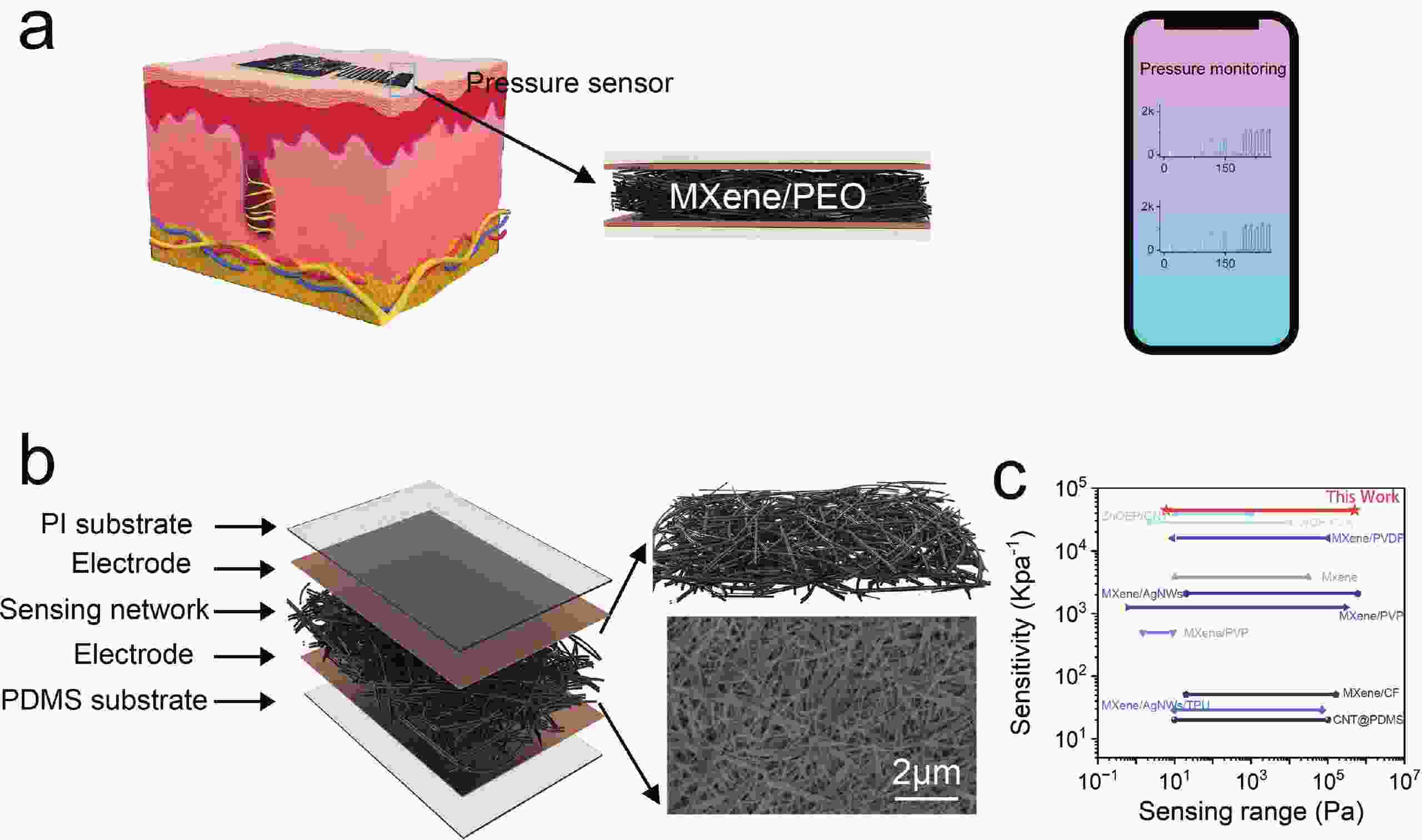
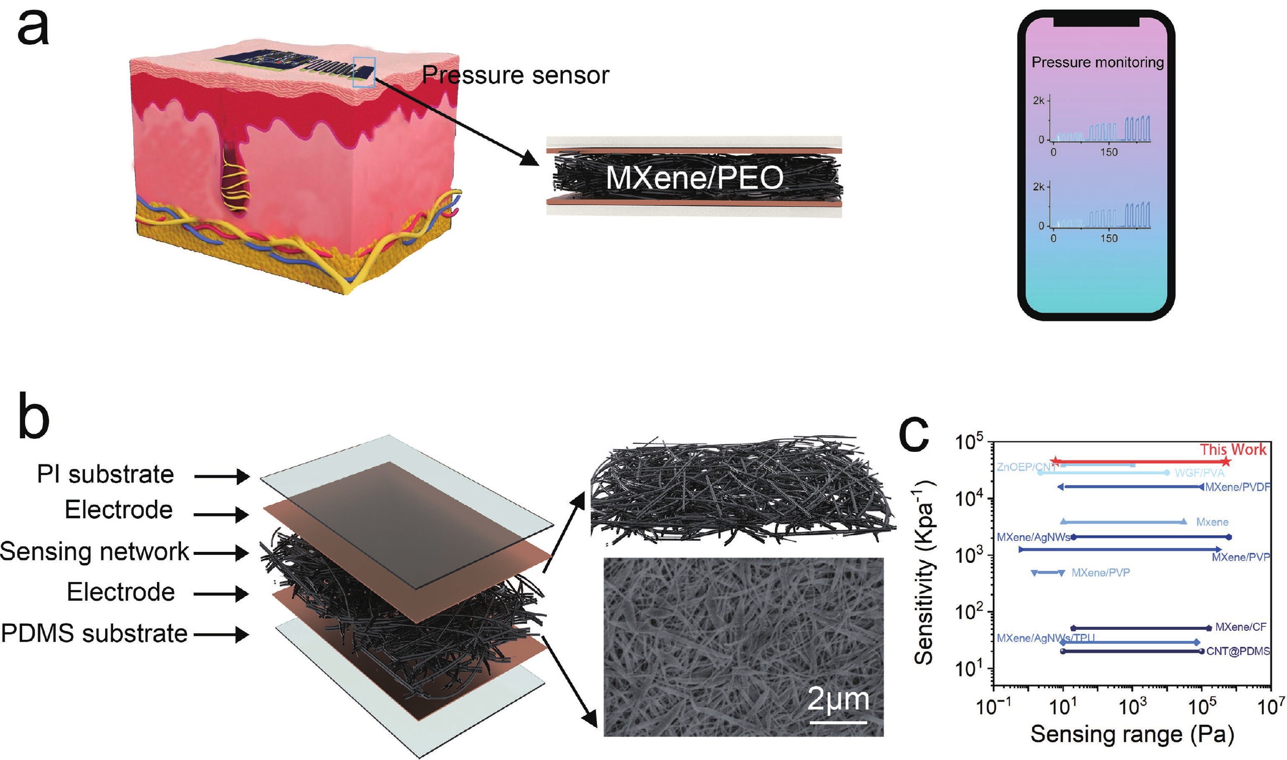
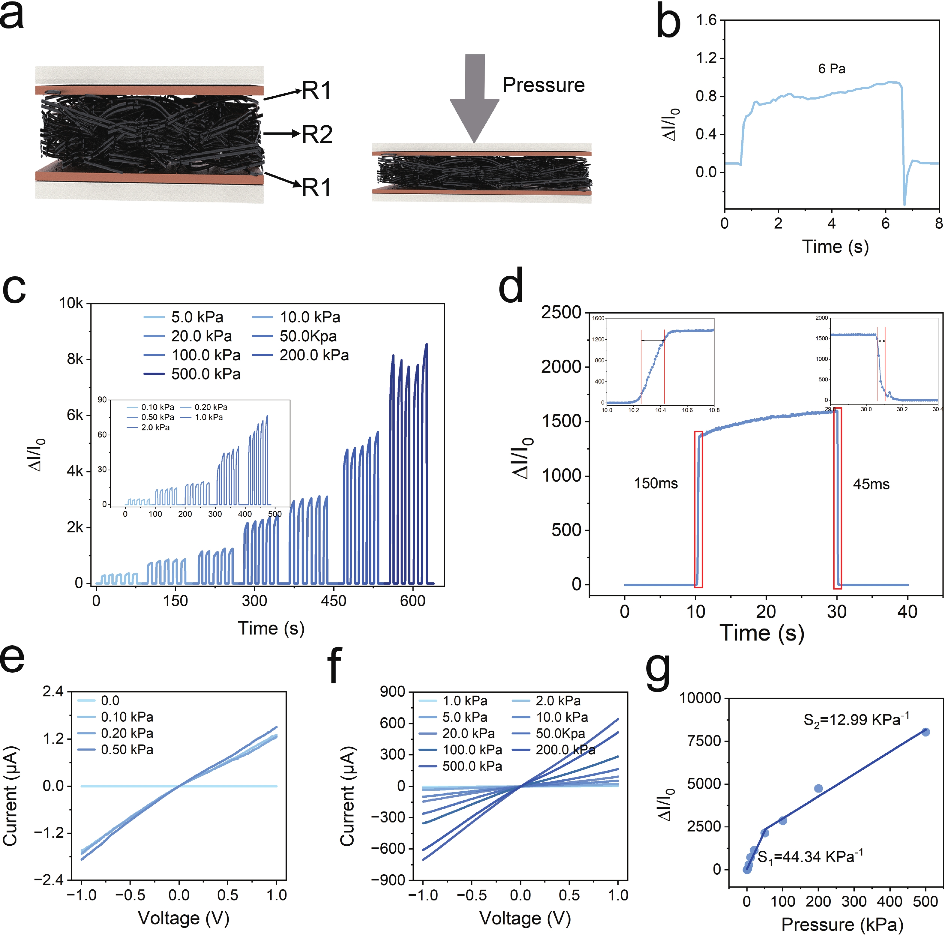
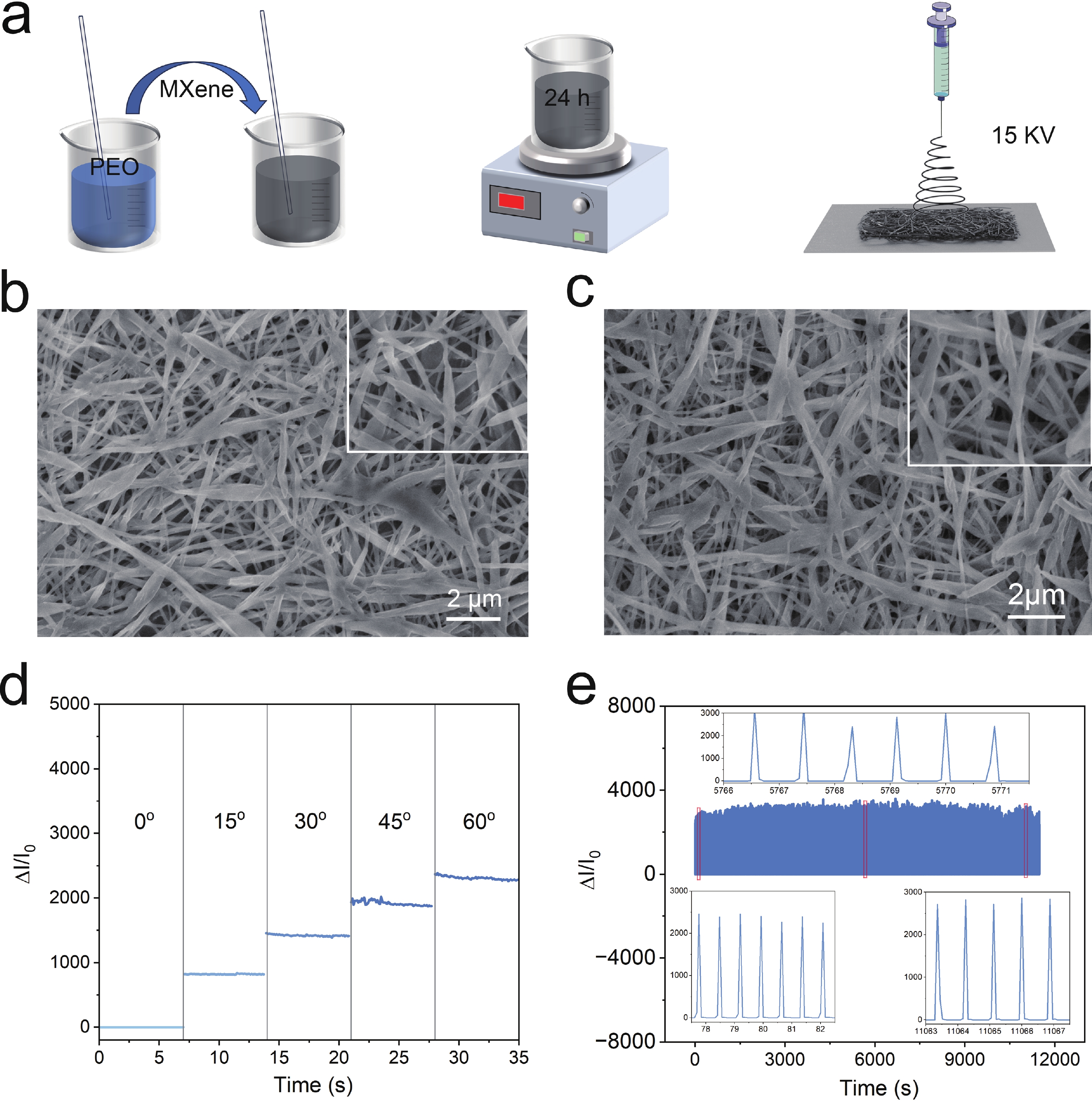
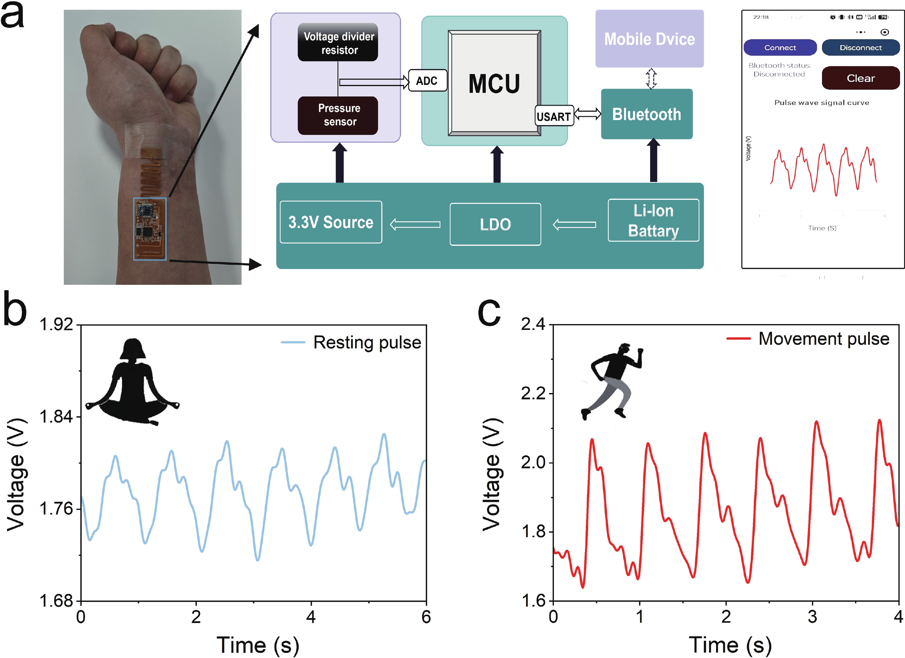
High-performance flexible pressure sensors have garnered significant attention in fields such as wearable electronics and human-machine interfaces. However, the development of flexible pressure sensors that simultaneously achieve high sensitivity, a wide detection range, and good mechanical stability remains a challenge. In this paper, we propose a flexible piezoresistive pressure sensor based on a Ti3C₂Tx (MXene)/polyethylene oxide (PEO) composite nanofiber membrane (CNM). The sensor, utilizing MXene (0.4 wt%)/PEO (5 wt%), exhibits high sensitivity (44.34 kPa−1 at 0−50 kPa, 12.99 kPa−1 at 50−500 kPa) and can reliably monitor physiological signals and other subtle cues. Moreover, the sensor features a wide detection range (0−500 kPa), fast response and recovery time (~150/45 ms), and excellent mechanical stability (over 10 000 pressure cycles at maximum load). Through an MXene/PEO sensor array, we demonstrate its applications in human physiological signal monitoring, providing a reliable way to expand the application of MXene-based flexible pressure sensors.
J. Semicond.
2025, 46(4): 042701 doi: 10.1088/1674-4926/24110002
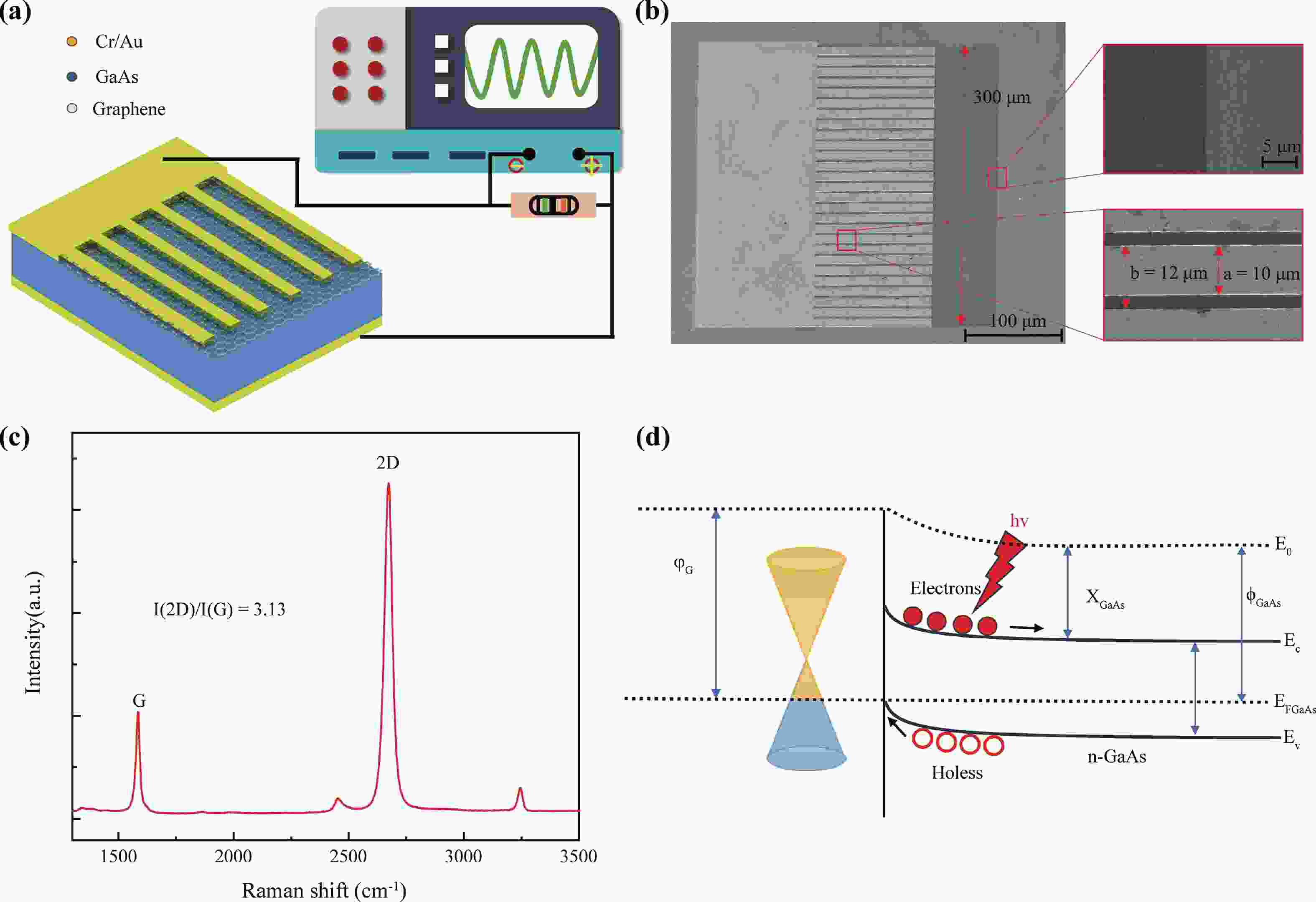
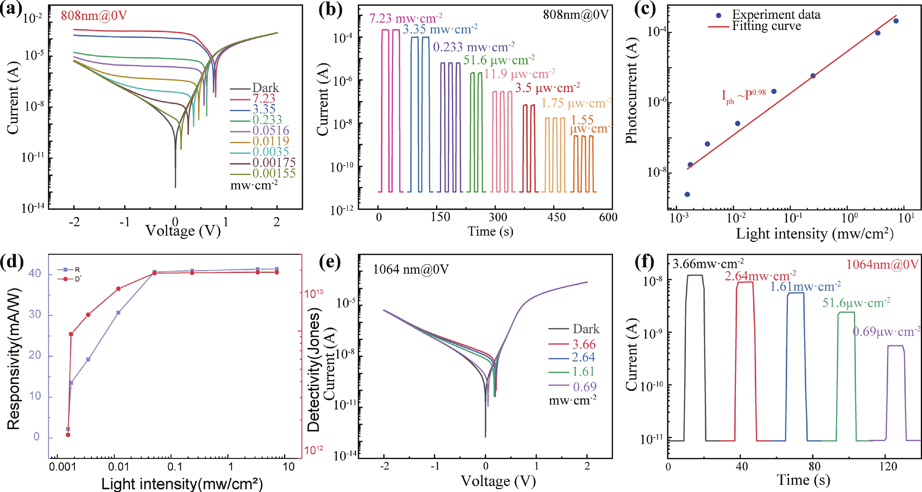
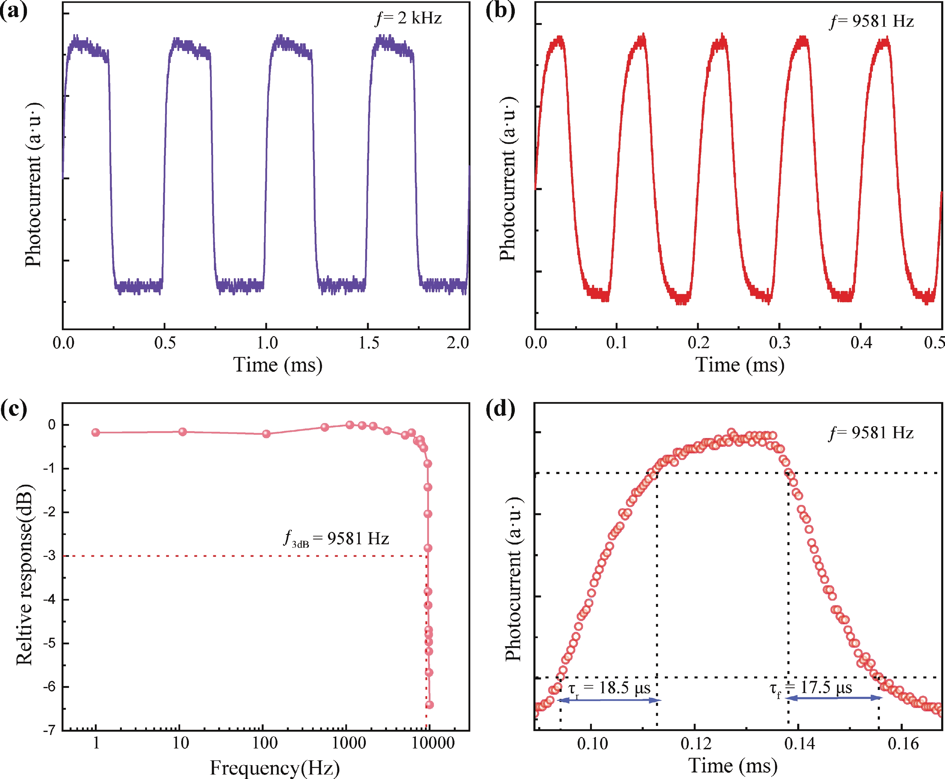
In the rapidly evolving field of modern technology, near-infrared (NIR) photodetectors are extremely crucial for efficient and reliable optical communications. The graphene/GaAs Schottky junction photodetector leverages graphene’s exceptional carrier mobility and broadband absorption, coupled with GaAs’s strong absorption in the NIR spectrum, to achieve high responsivity and rapid response times. Here, we present a NIR photodetector employing a graphene/GaAs Schottky junction tailored for communication wavelengths. We fabricated high-performance graphene/GaAs Schottky junction devices with interdigitated electrodes of varying finger widths, systematically investigating their impact on device performance. The experimental results demonstrate that incorporating interdigitated electrodes significantly enhances the collection efficiency of photogenerated carriers in graphene/GaAs photodetectors. When illuminated by 808 nm NIR light at an intensity of 7.23 mW/cm2, the device achieves an impressive switch ratio of 10⁷, along with a high responsivity of 40.1 mA/W and a remarkable detectivity of 2.89 × 10¹³ Jones. Additionally, the device is characterized by rapid response times, with rise and fall times of 18.5 and 17.5 μs, respectively, at a 3 dB bandwidth. These findings underscore the significant potential of high-performance graphene/GaAs photodetectors for applications in NIR optoelectronic systems.


J. Semicond.
2025, 46(4): 042702 doi: 10.1088/1674-4926/24090023

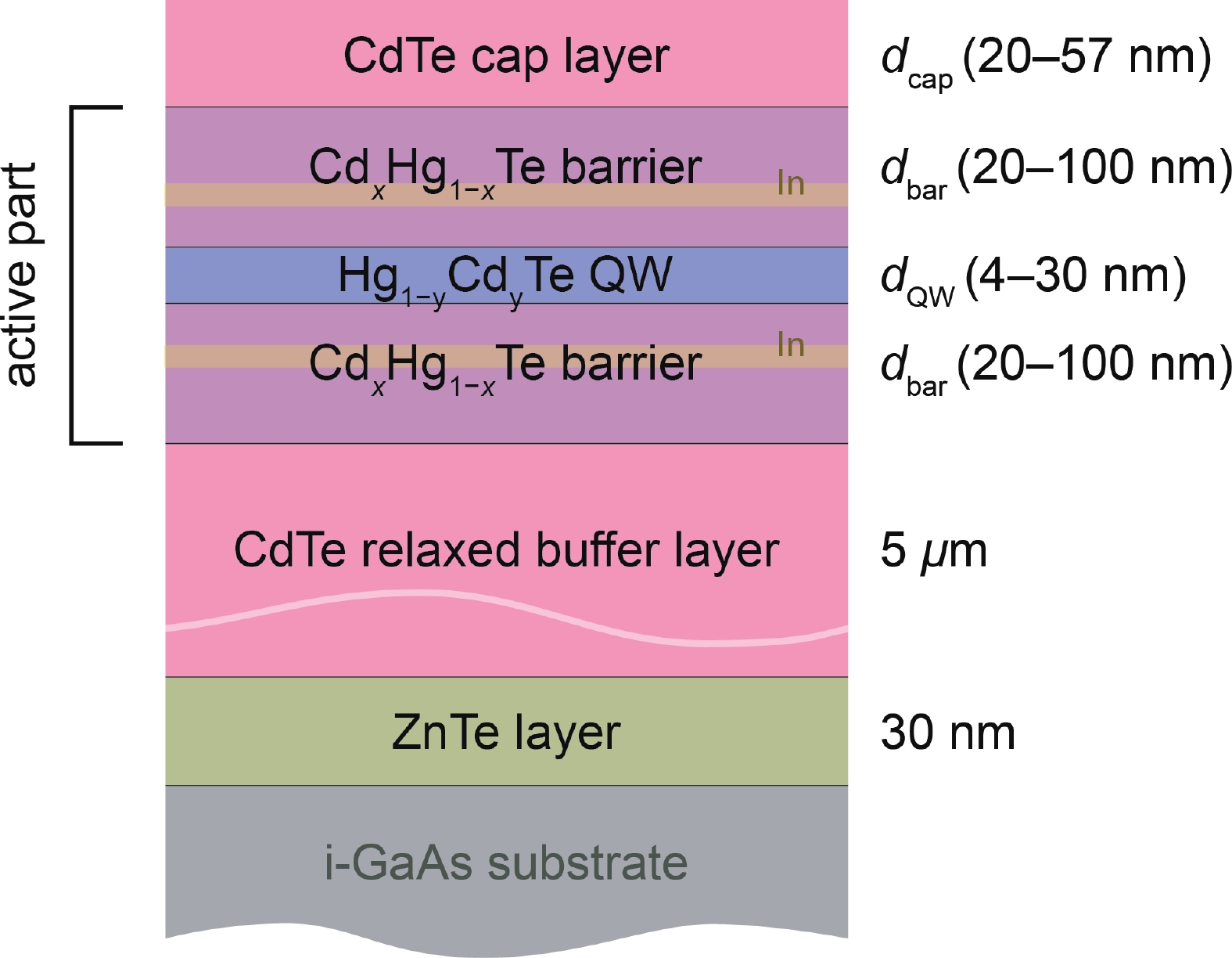
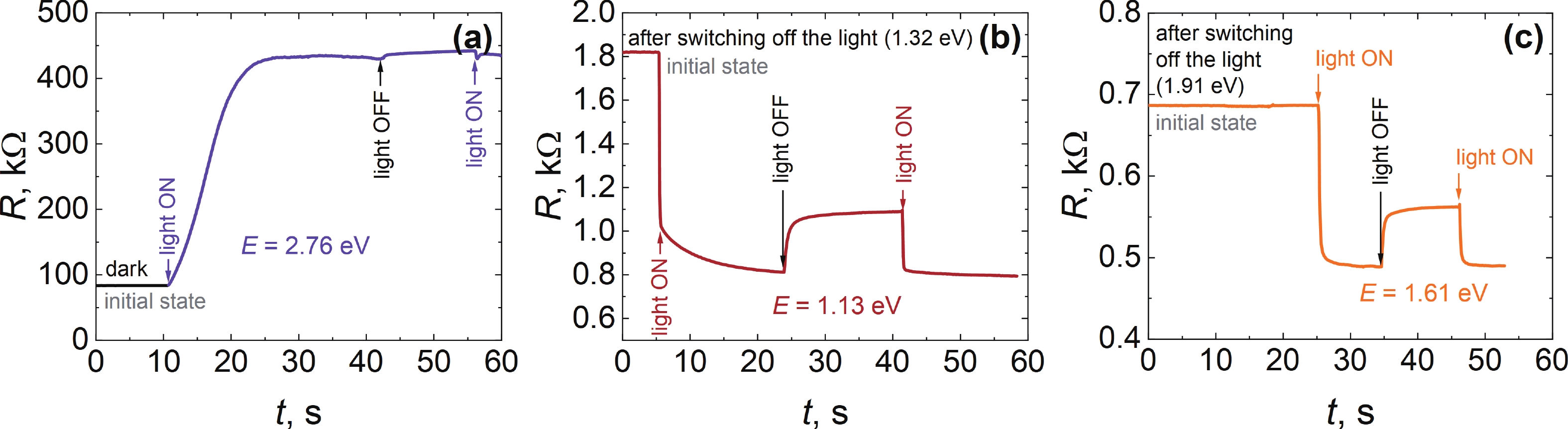
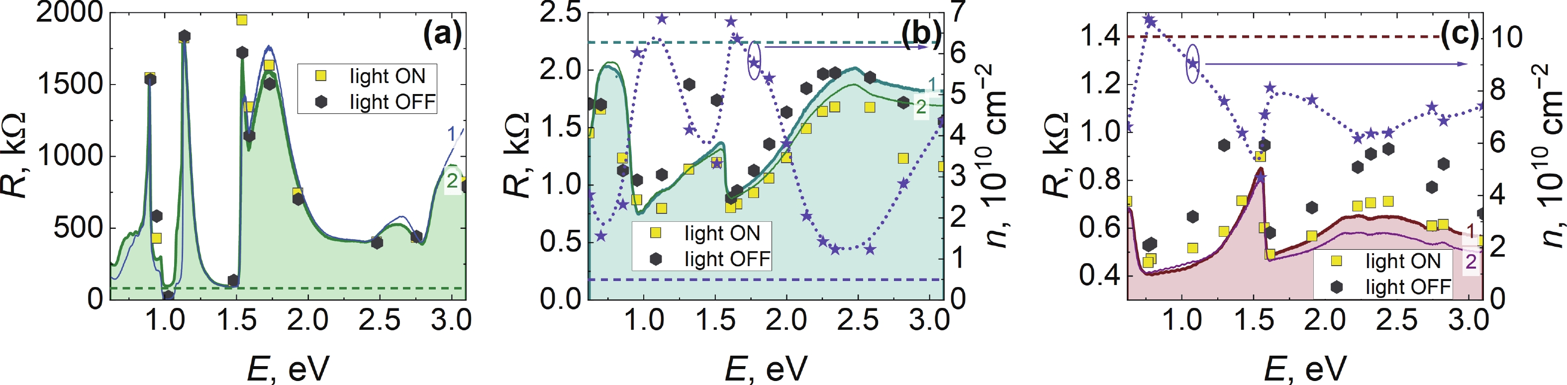
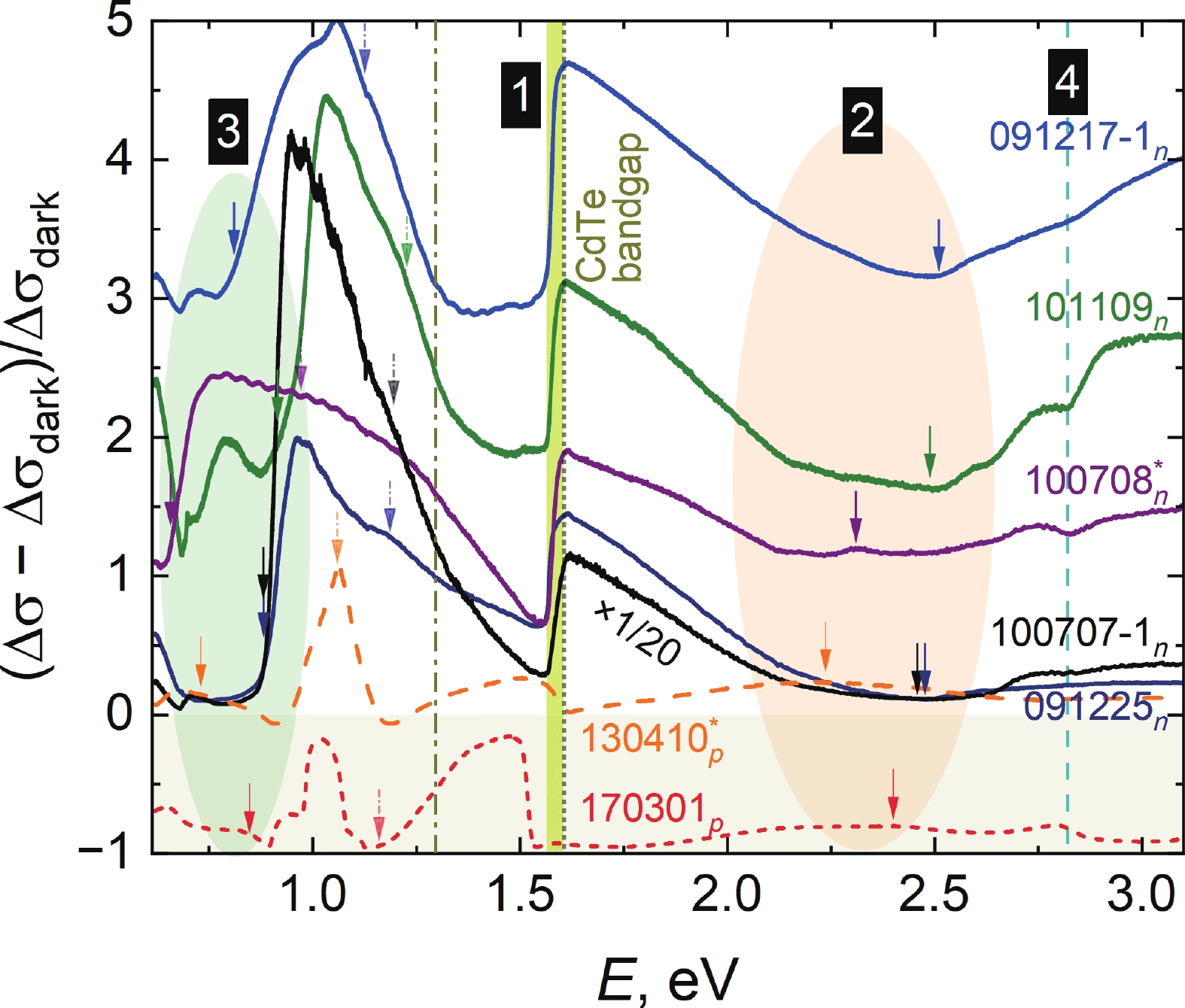
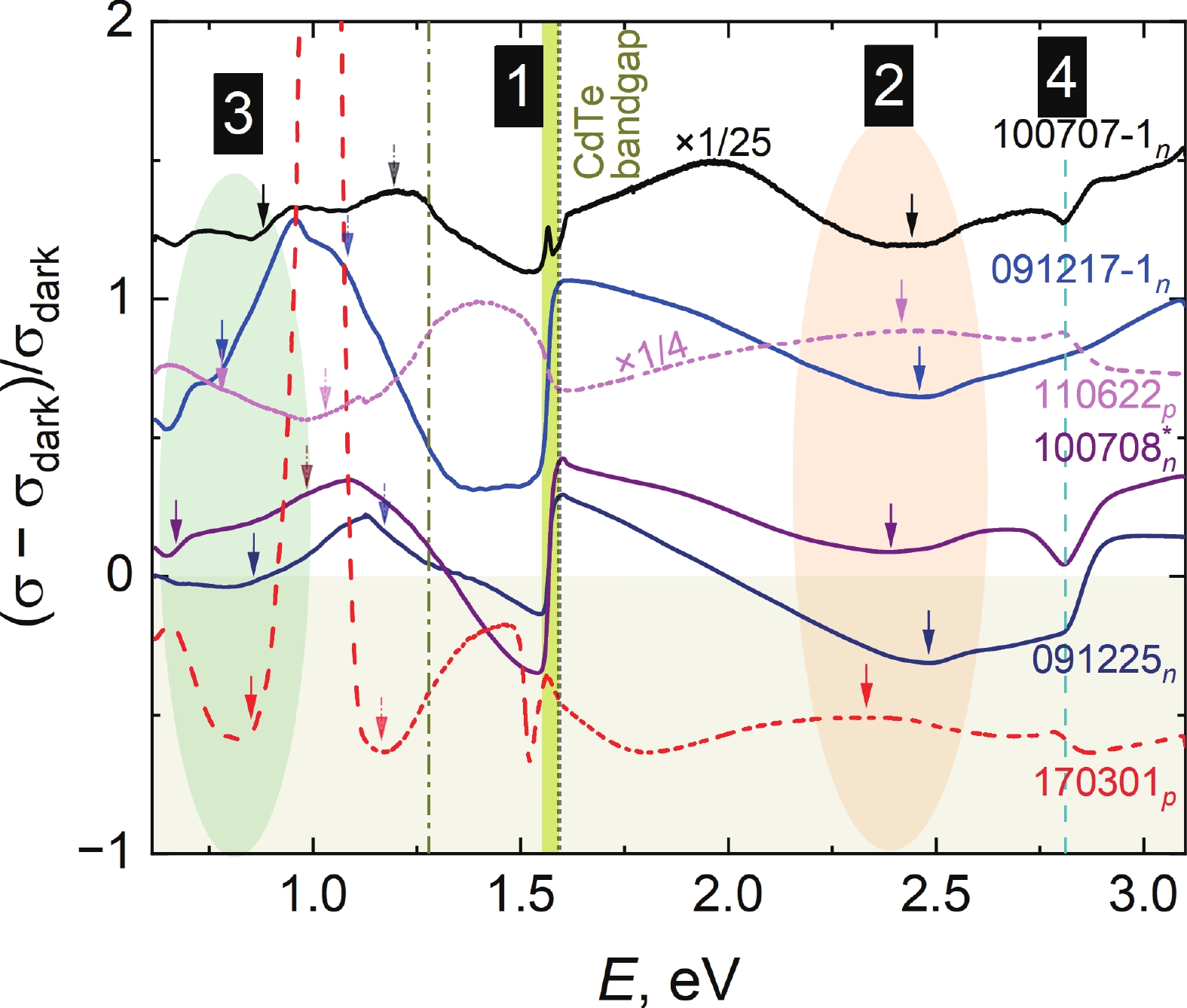
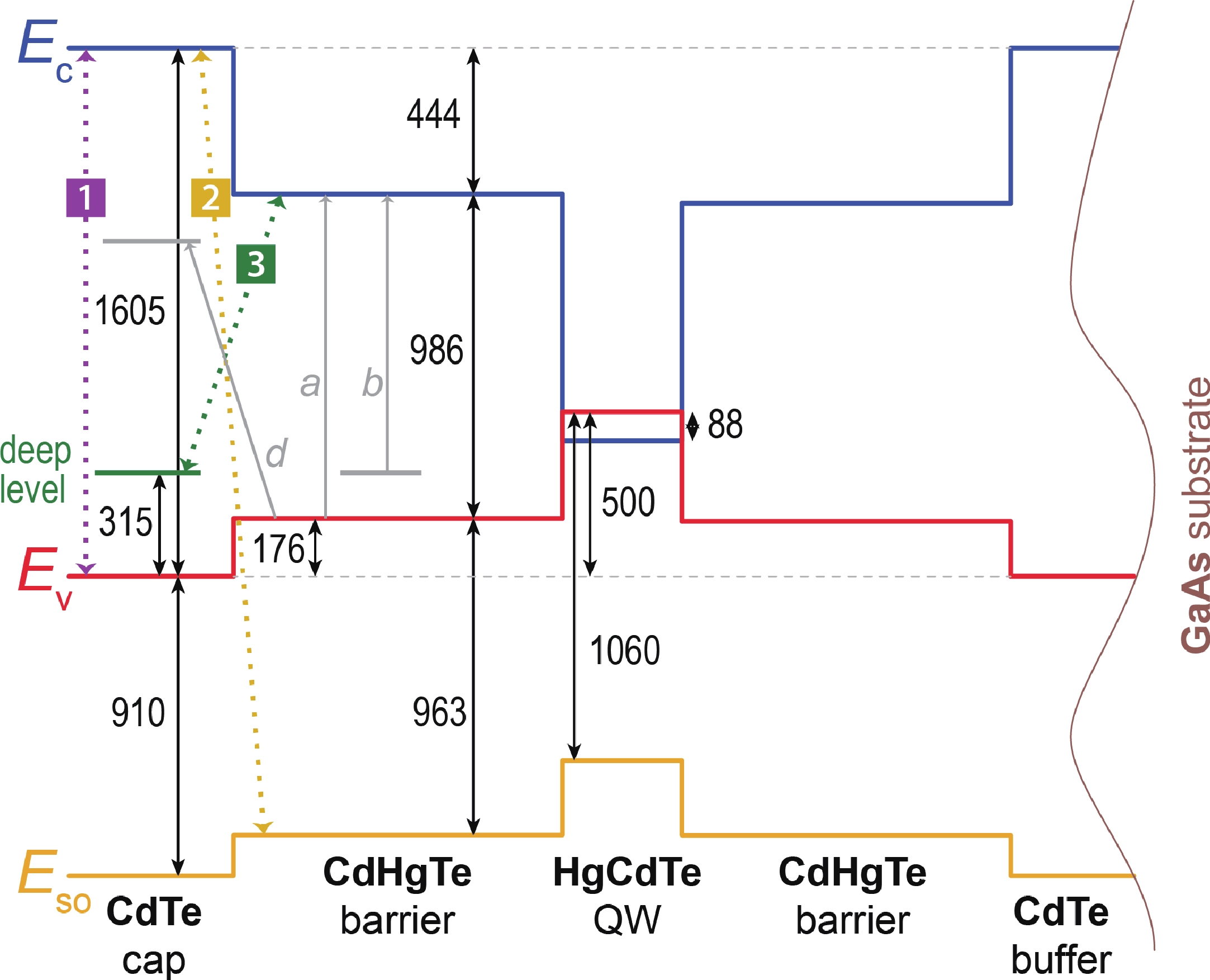
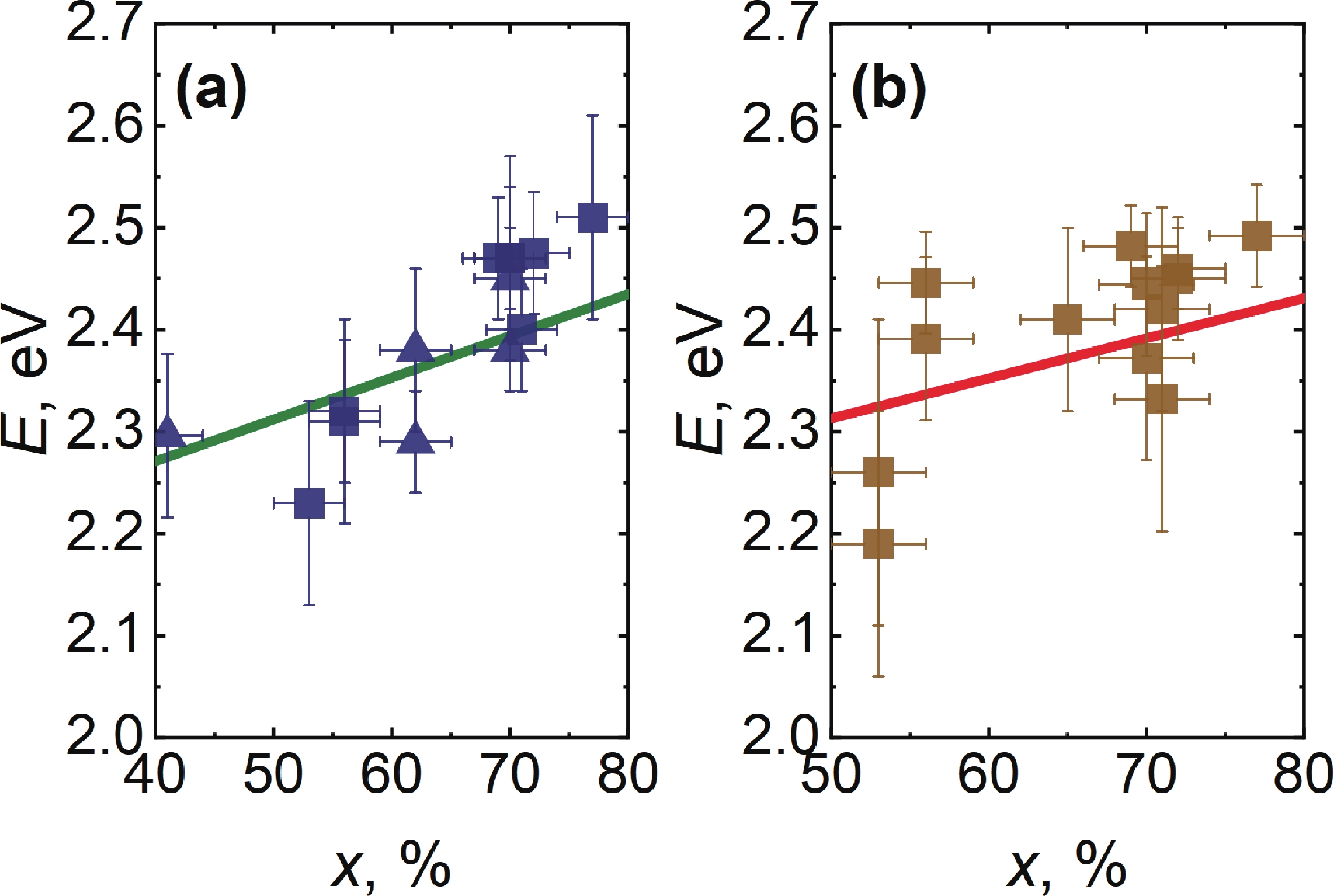
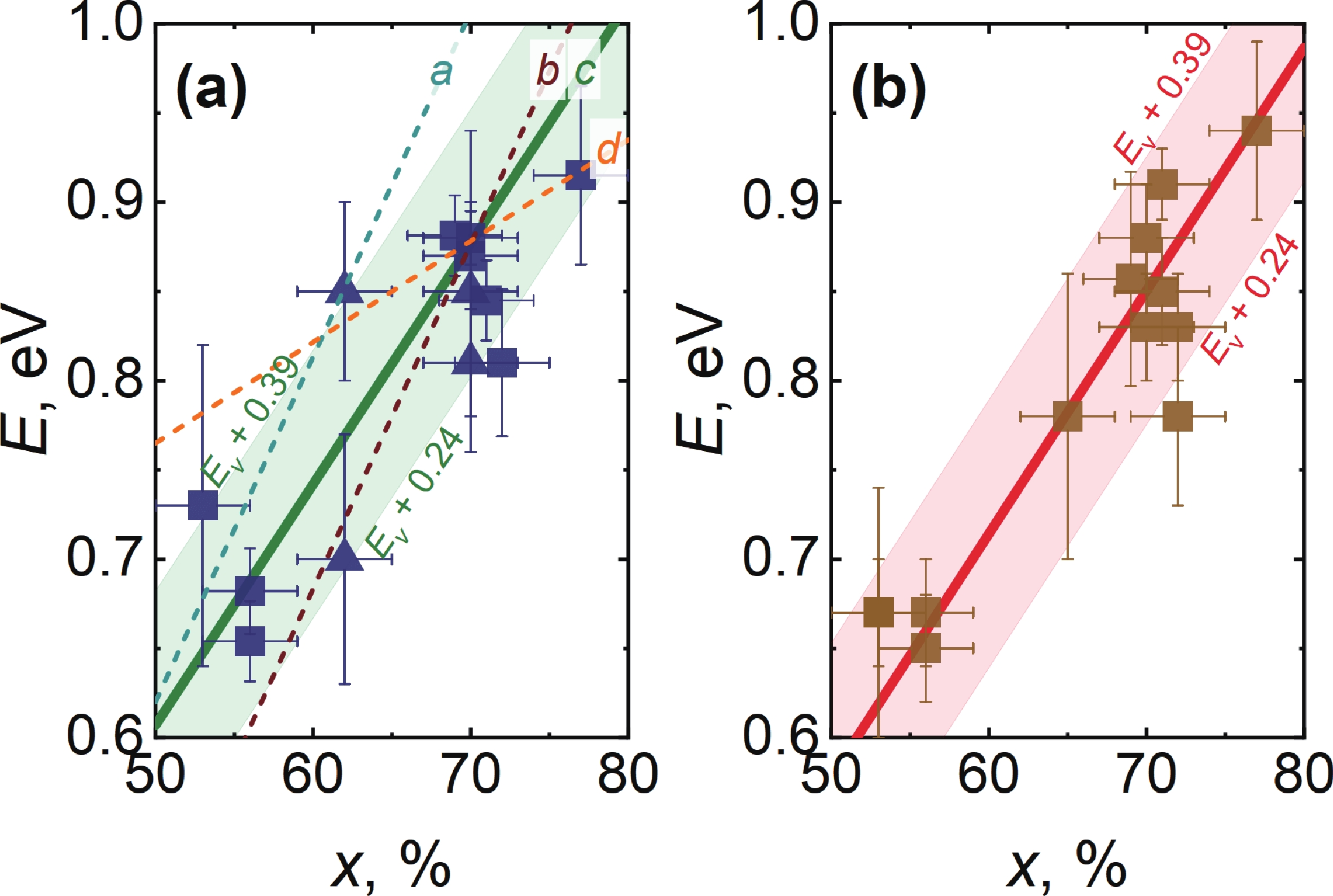
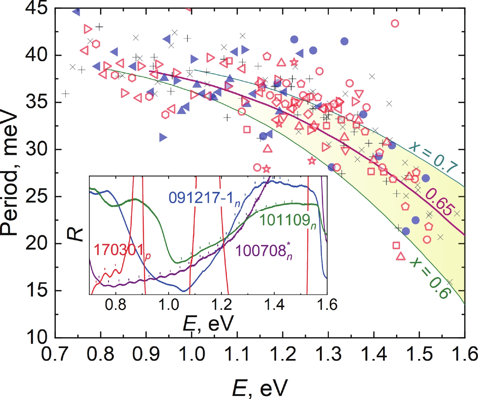
In this work, we studied the persistent photoconductivity (PPC) spectra in single HgTe/CdHgTe quantum wells with different growth parameters and different types of dark conductivity. The studies were performed in a wide radiation quantum energy range of 0.62–3.1 eV both at T = 4.2 K and at T = 77 K. Common features of the PPC spectra for all structures were revealed, and their relation to the presence of a CdTe cap layer in all structures and the appropriate cadmium fraction in the CdHgTe barrier layers was shown. One of the features was associated with the presence of a deep level in the CdTe layer. In addition, the oscillatory behavior of the PPC spectra in the region from 0.8–1.1 eV to 1.2–1.5 eV was observed. It is associated with the cascade emission of longitudinal optical phonons in CdHgTe barrier.
J. Semicond.
2025, 46(4): 042703 doi: 10.1088/1674-4926/24090034
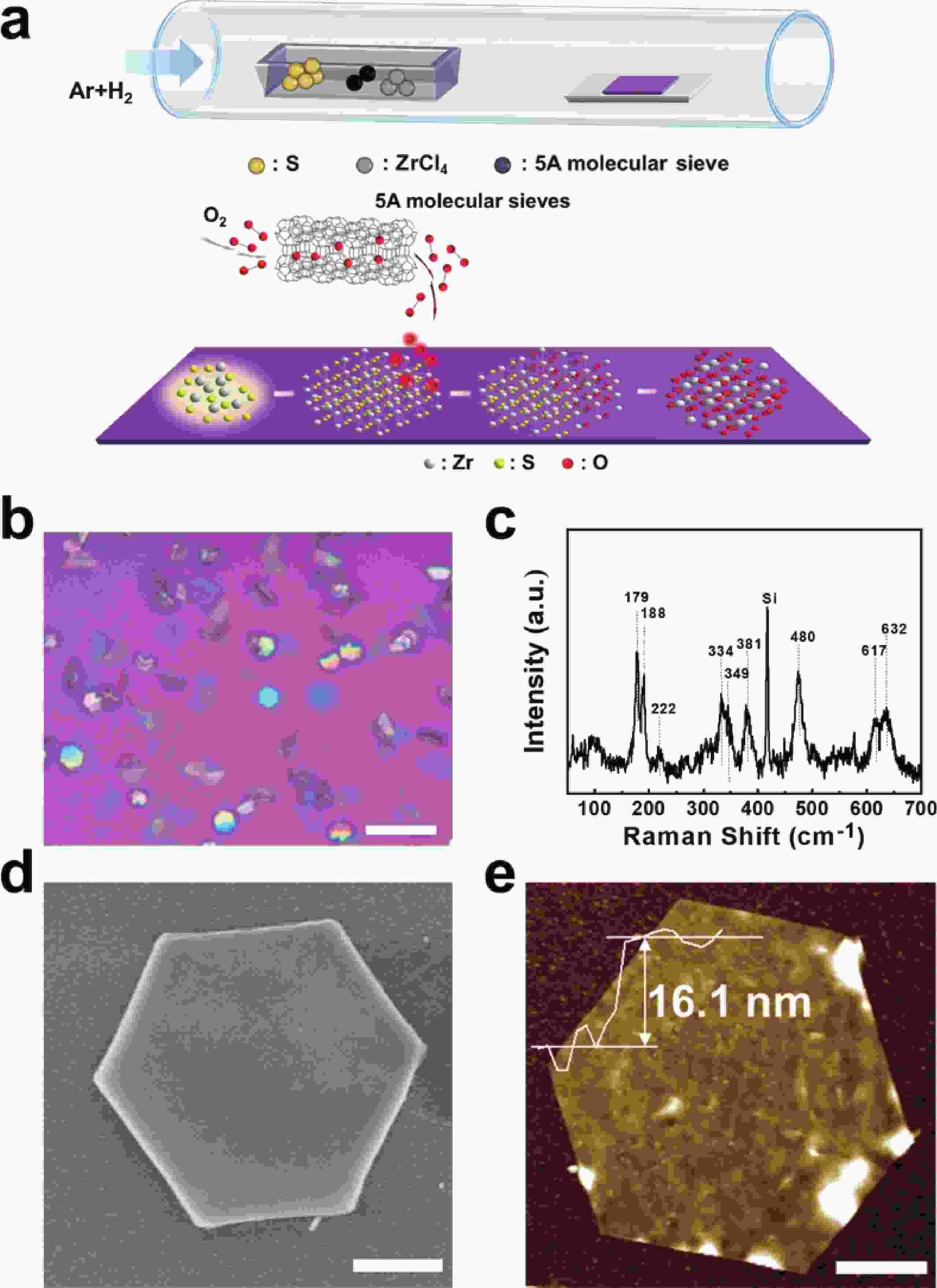
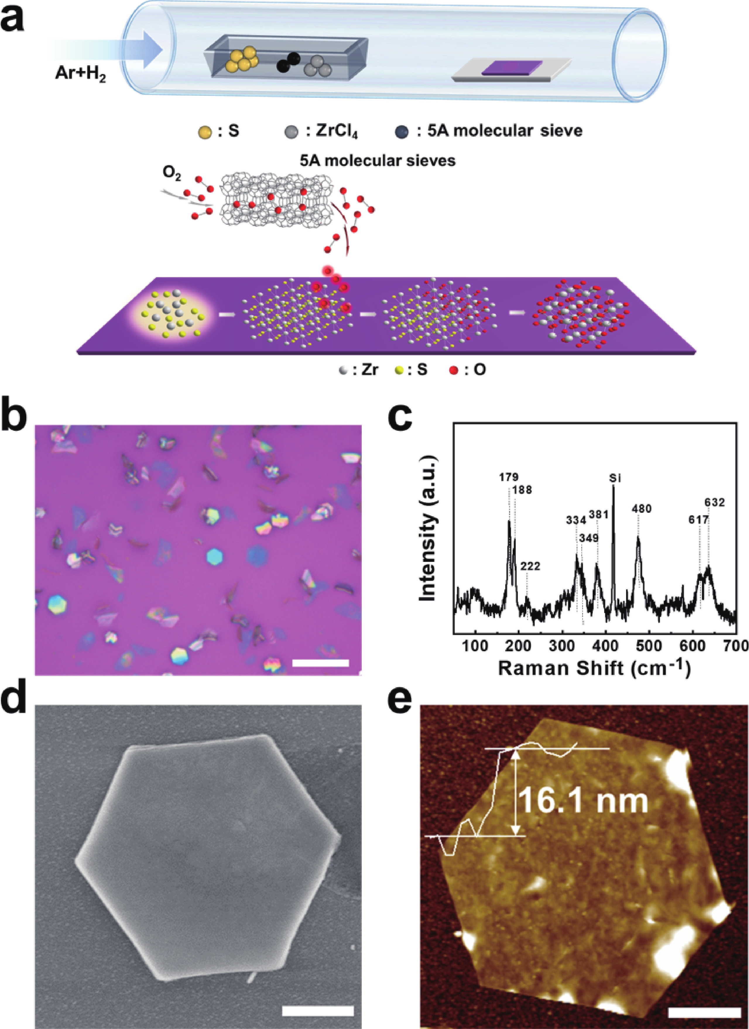
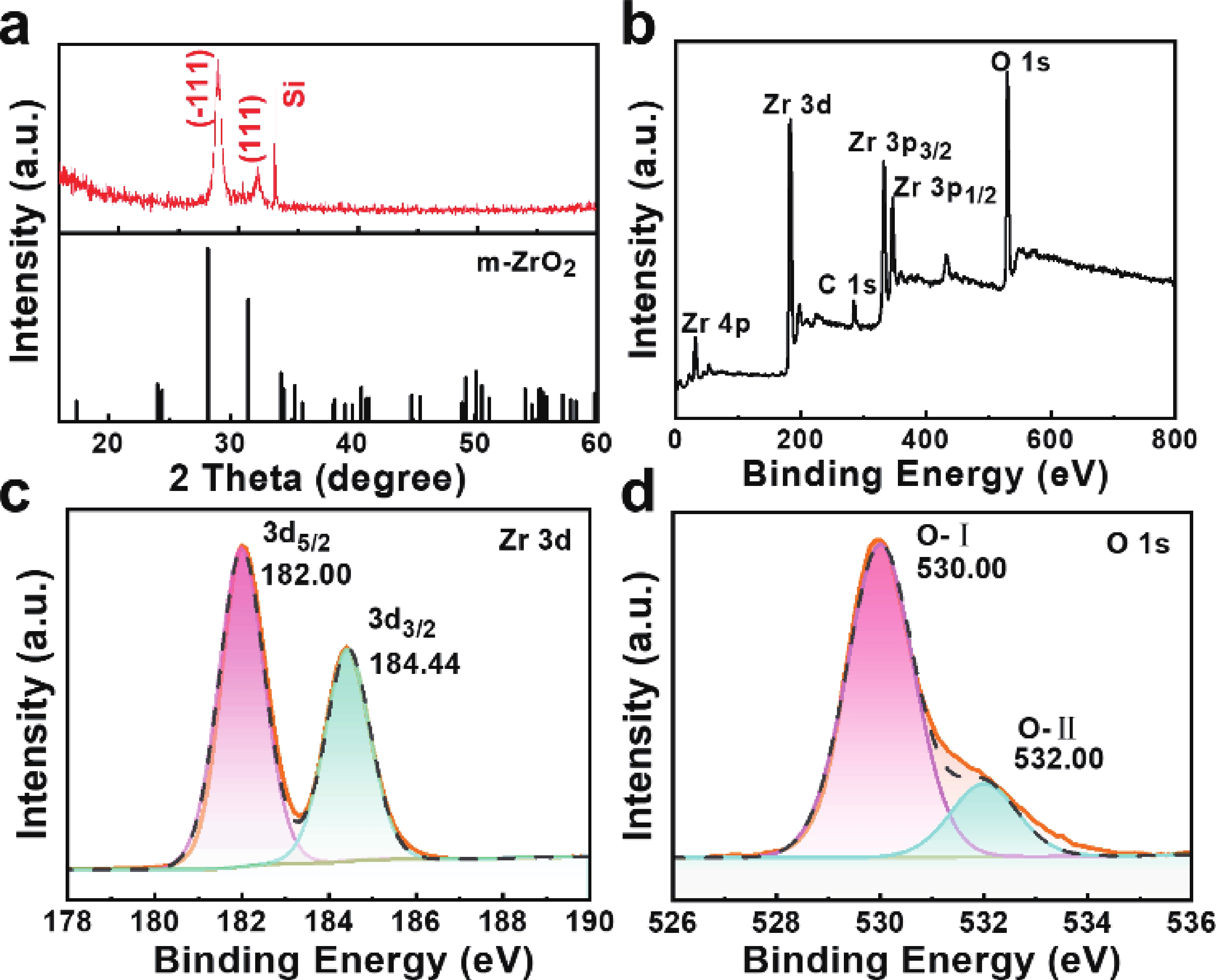
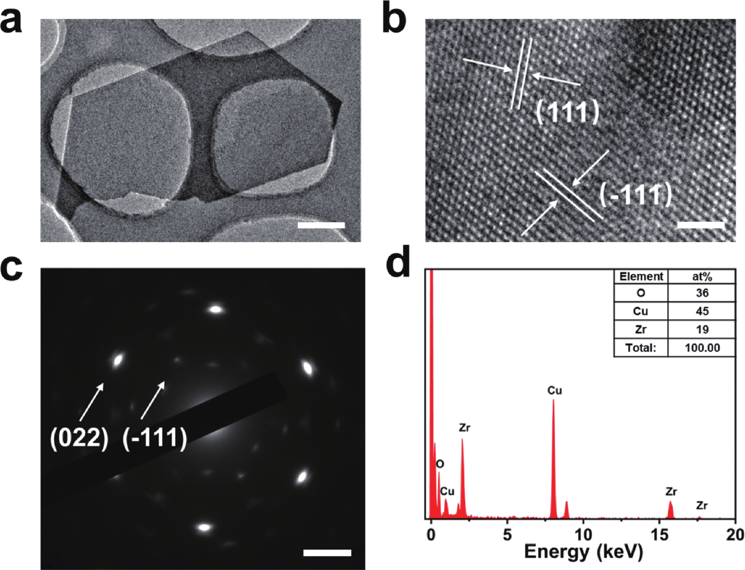
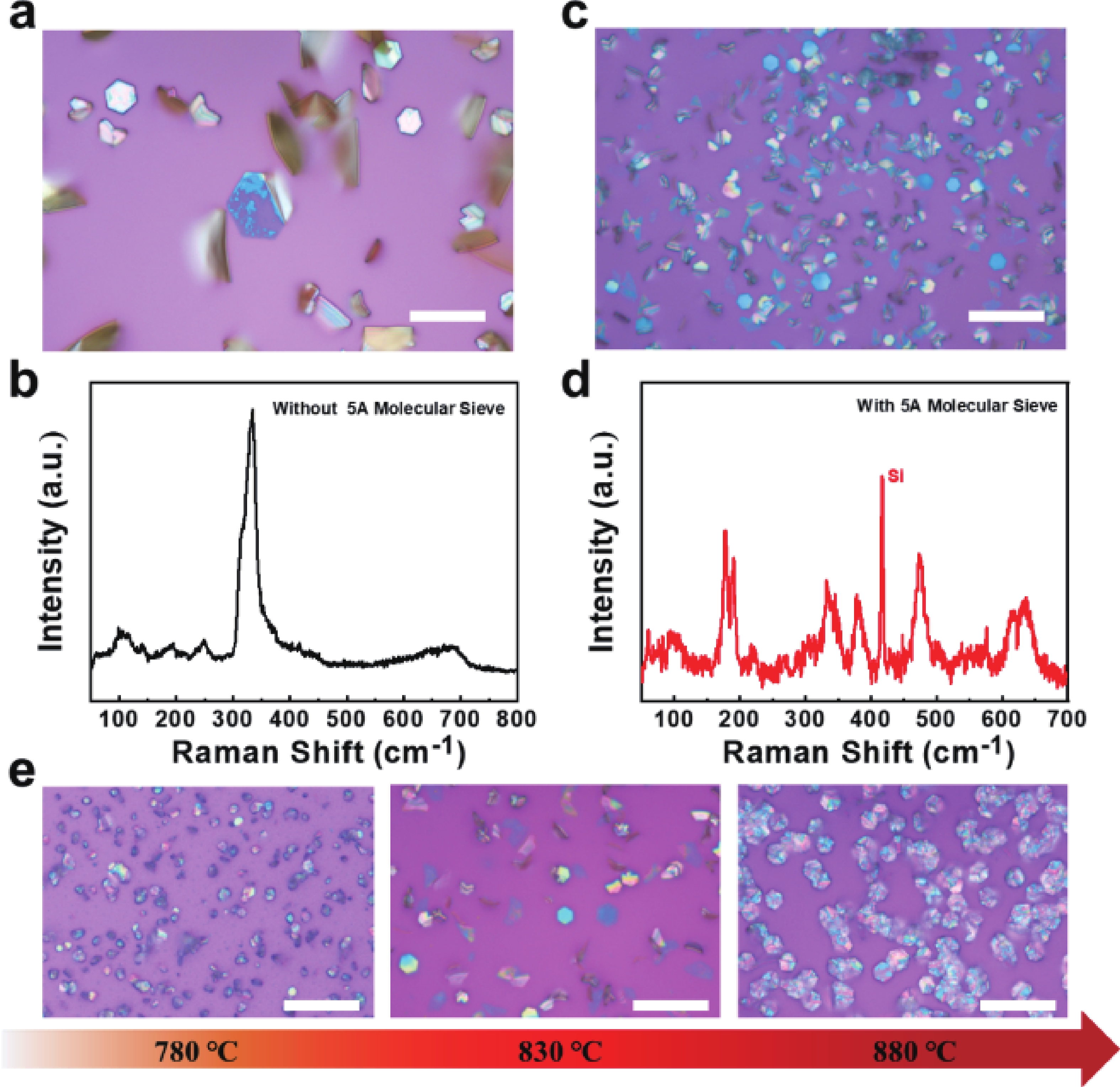
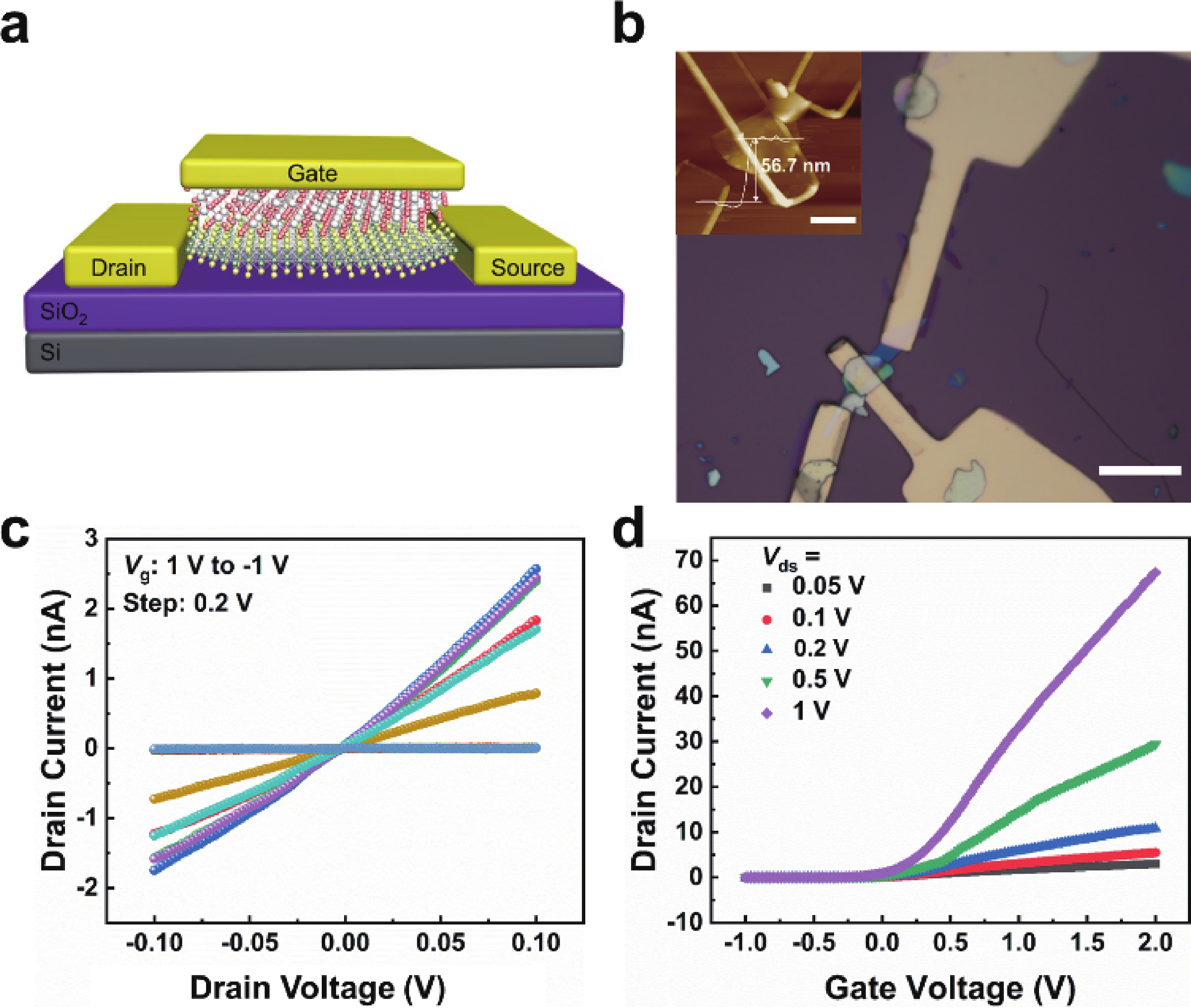
In order to address challenges posed by the reduction in transistor size, researchers are concentrating on two-dimensional (2D) materials with high dielectric constants and large band gaps. Monoclinic ZrO2 (m-ZrO2) has emerged as a promising gate dielectric material due to its suitable dielectric constant, wide band gap, ideal valence-band offset, and good thermodynamic stability. However, current deposition methods face compatibility issues with 2D semiconductors, highlighting the need for high-quality dielectrics and interfaces. Here, high-quality 2D m-ZrO2 single crystals are successfully prepared using a one-step chemical vapor deposition (CVD) method, aided by 5A molecular sieves for oxygen supply. The prepared ZrO2 is utilized as a gate dielectric in the construction of MoS2 field-effect transistors (FETs) to investigate its electrical property. The FETs exhibit a high carrier mobility of up to 5.50 cm2·V−1·s−1, and a current switching ratio (Ion/off) of approximately 104, which aligns with the current standards of logic circuits, indicating that ZrO2 has application value as a gate dielectric. The successful one-step preparation of single-crystal ZrO2 paves the way for the utilization of high-κ gate dielectrics and creates favorable conditions for the development of high-performance semiconductor devices, offering new possibilities for transistor miniaturization.