Semiconductor materials exemplify humanity's unwavering pursuit of enhanced performance, efficiency, and functionality in electronic devices. From its early iterations to the advanced variants of today, this field has undergone an extraordinary evolution. As the reliability requirements of integrated circuits continue to increase, the industry is placing greater emphasis on the crystal qualities. Consequently, conducting a range of characterization tests on the crystals has become necessary. This paper will examine the correlation between crystal quality, device performance, and production yield, emphasizing the significance of crystal characterization tests and the important role of high-precision synchrotron radiation X-ray topography characterization in semiconductor analysis. Finally, we will cover the specific applications of synchrotron radiation characterization in the development of semiconductor materials.
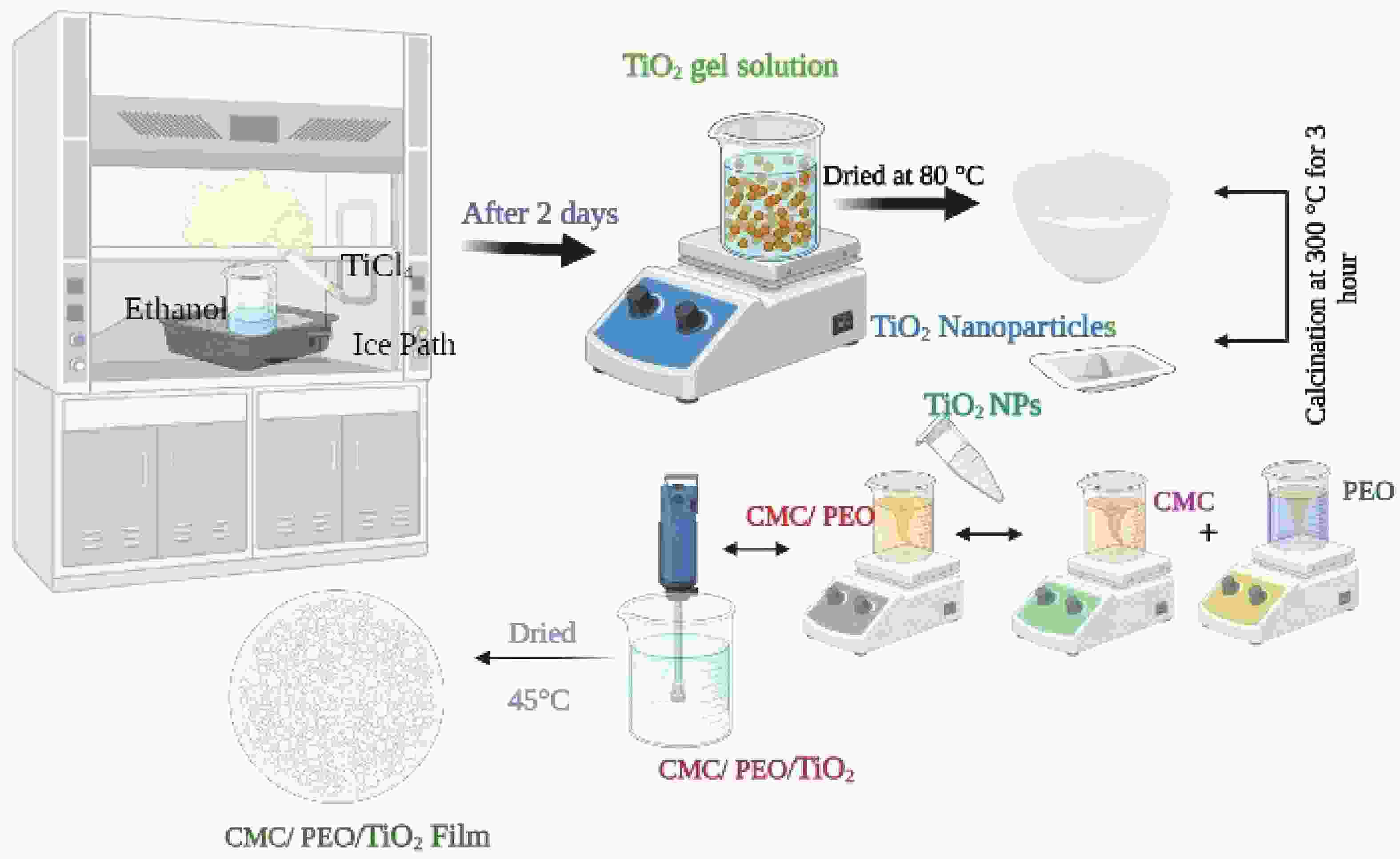
Nanocomposite films consisting of carboxymethyl cellulose, polyethylene oxide (CMC/PEO), and anatase titanium dioxide (TO) were produced by the use of sol-gel and solution casting techniques. TiO2 nanocrystals were effectively incorporated into CMC/PEO polymers, as shown by X-ray diffraction (XRD) and attenuated total reflectance fourier transform infrared (ATR-FTIR) analysis. The roughness growth is at high levels of TO nanocrystals (TO NCs), which means increasing active sites and defects in CMC/PEO. In differential scanning calorimetry (DSC) thermograms, the change in glass transition temperature (Tg) values verifies that the polymer blend interacts with TO NCs. The increment proportions of TO NCs have a notable impact on the dielectric performances of the nanocomposites, as observed. The electrical properties of the CMC/PEO/TO nanocomposite undergo significant changes. The nanocomposite films exhibit a red alteration in the absorption edge as the concentration of TO NCs increases in the polymer blend. The decline in the energy gap is readily apparent as the weight percentage of TO NCs increases. The photoluminescence (PL) emission spectra indicate that the sites of the luminescence peak maximums show slight variation; peaks get wider, while their intensities decrease dramatically as the concentration of TO increases. These nanocomposite materials show potential for multifunctional applications including optoelectronics, antireflection coatings, photocatalysis, light emitting diodes, and solid polymer electrolytes.
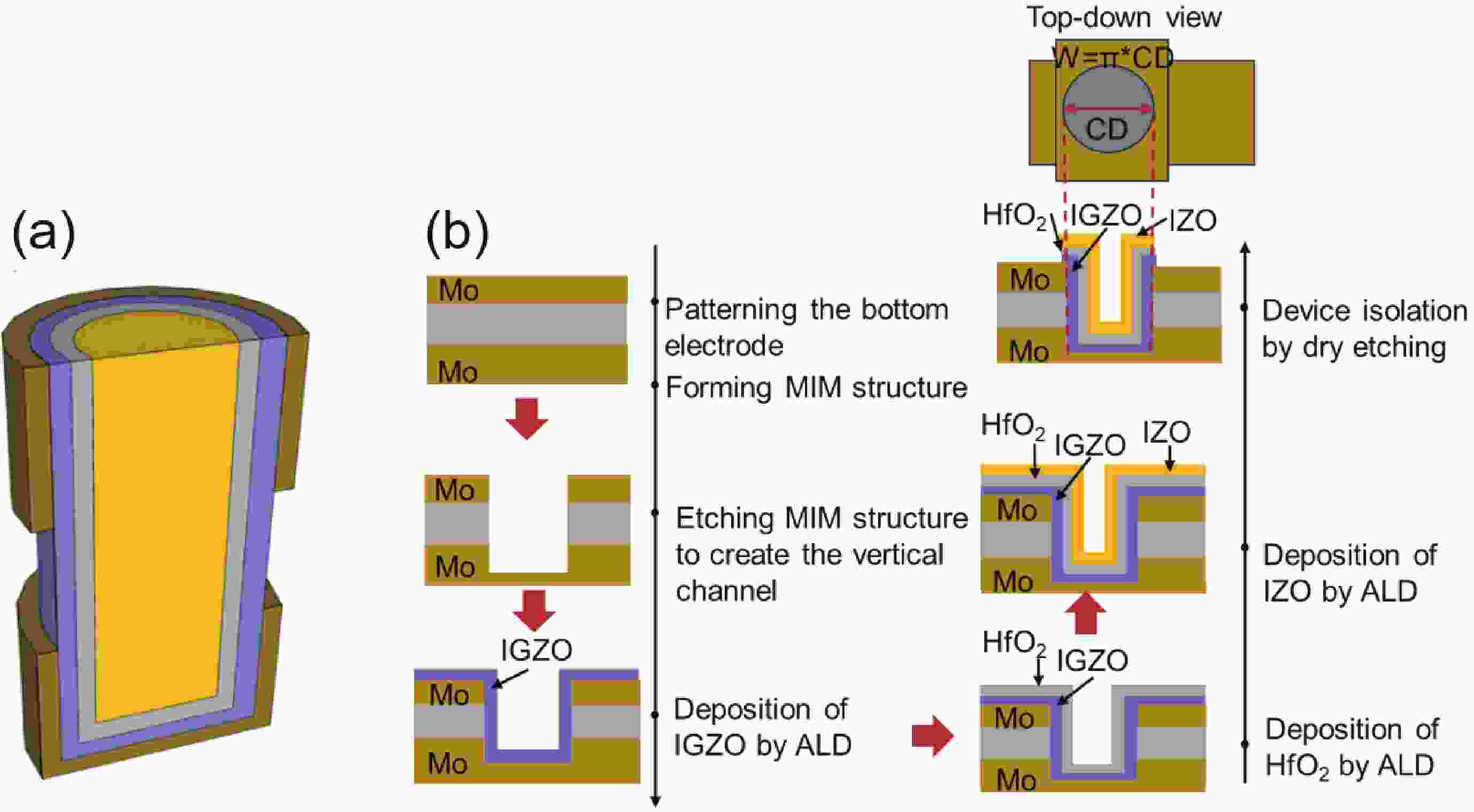
In–Ga–Zn–O (IGZO) channel based thin-film transistors (TFT), which exhibit high on–off current ratio and relatively high mobility, has been widely researched due to its back end of line (BEOL)-compatible potential for the next generation dynamic random access memory (DRAM) application. In this work, thermal atomic layer deposition (TALD) indium gallium zinc oxide (IGZO) technology was explored. It was found that the atomic composition and the physical properties of the IGZO films can be modulated by changing the sub-cycles number during atomic layer deposition (ALD) process. In addition, thin-film transistors (TFTs) with vertical channel-all-around (CAA) structure were realized to explore the influence of different IGZO films as channel layers on the performance of transistors. Our research demonstrates that TALD is crucial for high density integration technology, and the proposed vertical IGZO CAA-TFT provides a feasible path to break through the technical problems for the continuous scale of electronic equipment.
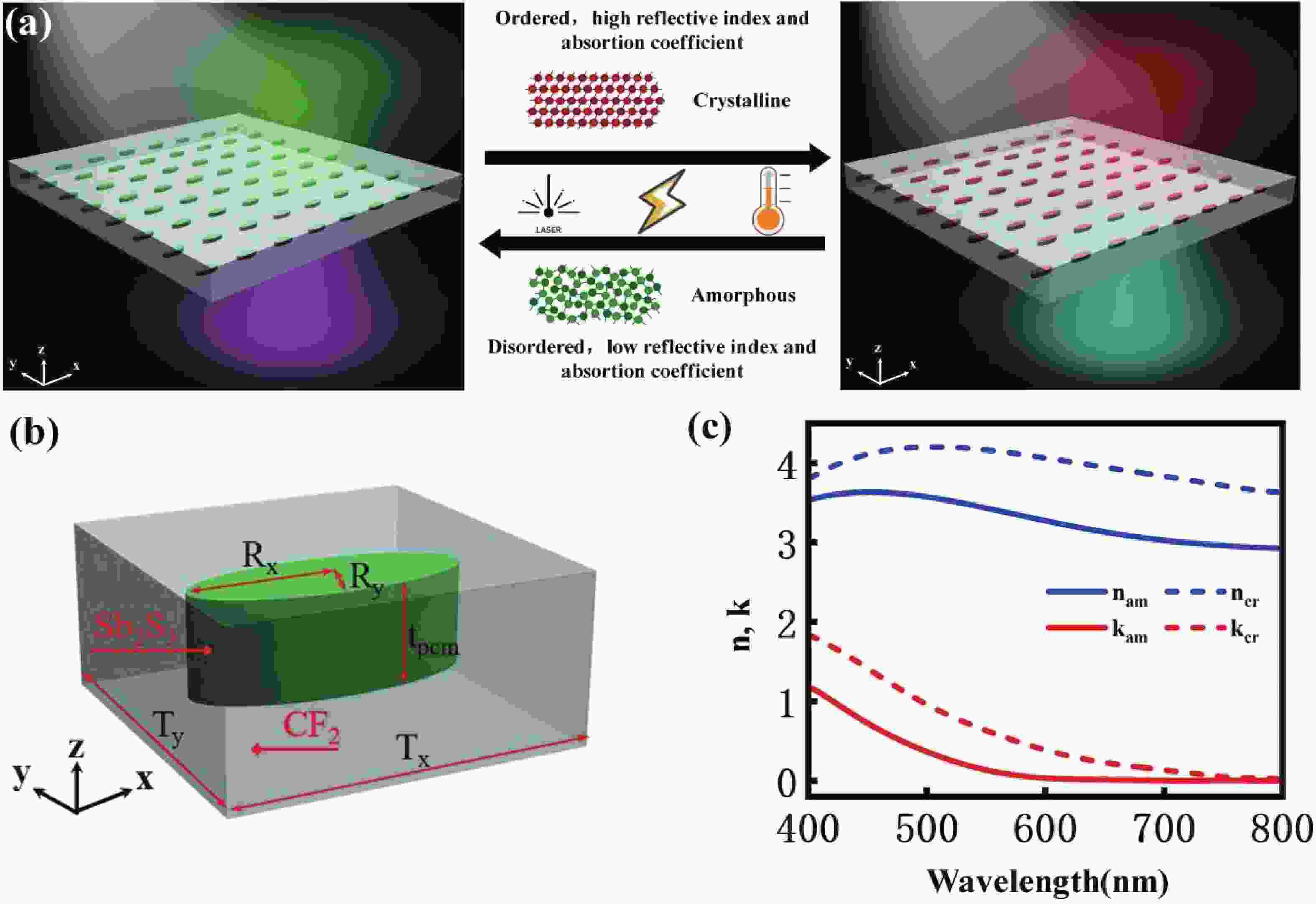
All-dielectric metasurface, which features low optical absorptance and high resolution, is becoming a promising candidate for full-color generation. However, the optical response of current metamaterials is fixed and lacks active tuning. In this work, we demonstrate a reconfigurable and polarization-dependent active color generation technique by incorporating low-loss phase change materials (PCMs) and CaF2 all-dielectric substrate. Based on the strong Mie resonance effect and low optical absorption structure, a transflective, full-color with high color purity and gamut value is achieved. The spectrum can be dynamically manipulated by changing either the polarization of incident light or the PCM state. High transmittance and reflectance can be simultaneously achieved by using low-loss PCMs and substrate. The novel active metasurfaces can bring new inspiration in the areas of optical encryption, anti-counterfeiting, and display technologies.
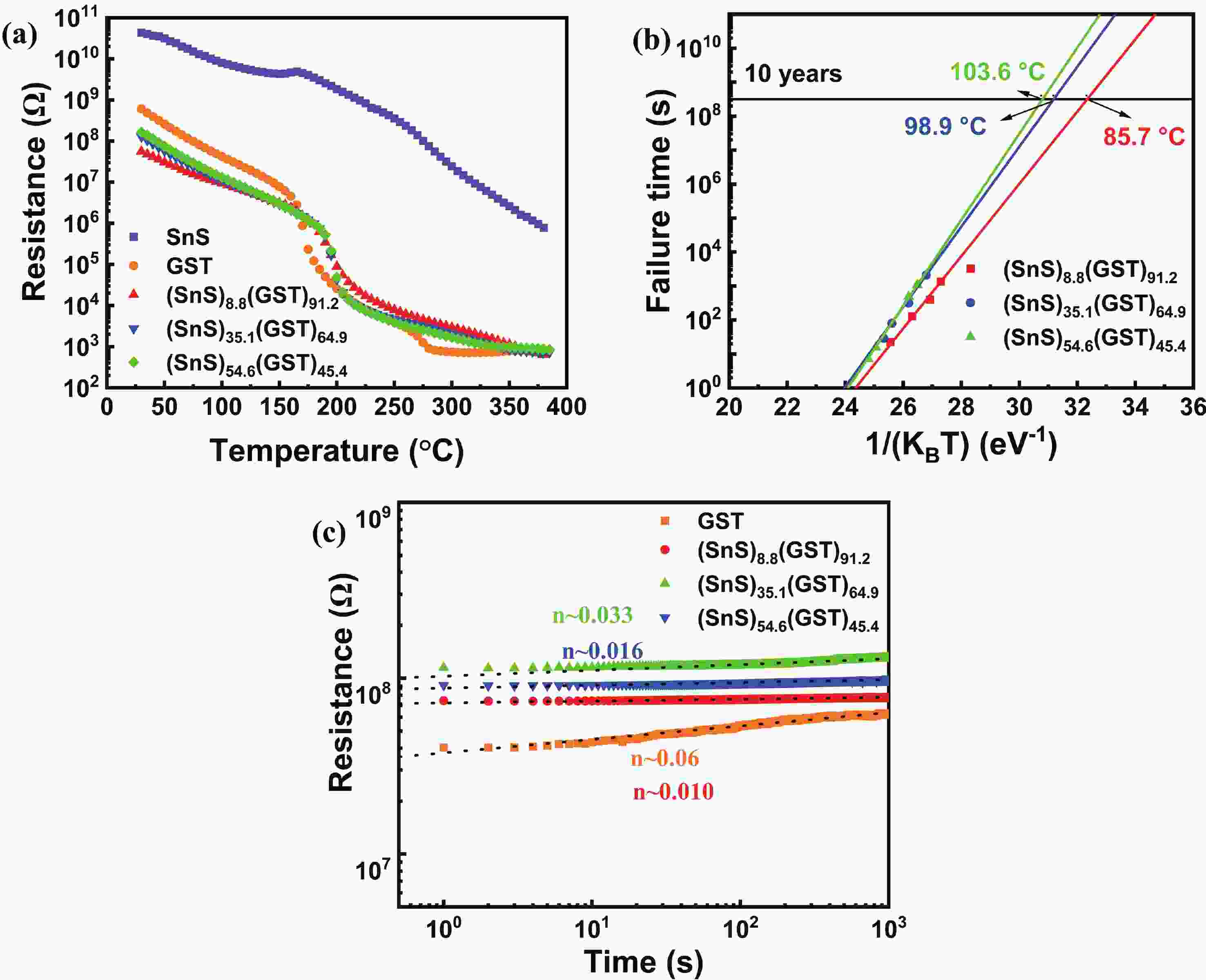
The amorphous phase-change materials with spontaneous structural relaxation leads to the resistance drift with the time for phase-change neuron synaptic devices. Here, we modify the phase change properties of the conventional Ge2Sb2Te5 (GST) material by introducing an SnS phase. It is found that the resistance drift coefficient of SnS-doped GST was decreased from 0.06 to 0.01. It can be proposed that the origin originates from the precipitation of GST nanocrystals accompanied by the precipitation of SnS crystals compared to single-phase GST compound systems. We also found that the decrease in resistance drift can be attributed to the narrowed bandgap from 0.65 to 0.43 eV after SnS-doping. Thus, this study reveals the quantitative relationship between the resistance drift and the band gap and proposes a new idea for alleviating the resistance drift by composition optimization, which is of great significance for finding a promising phase change material.
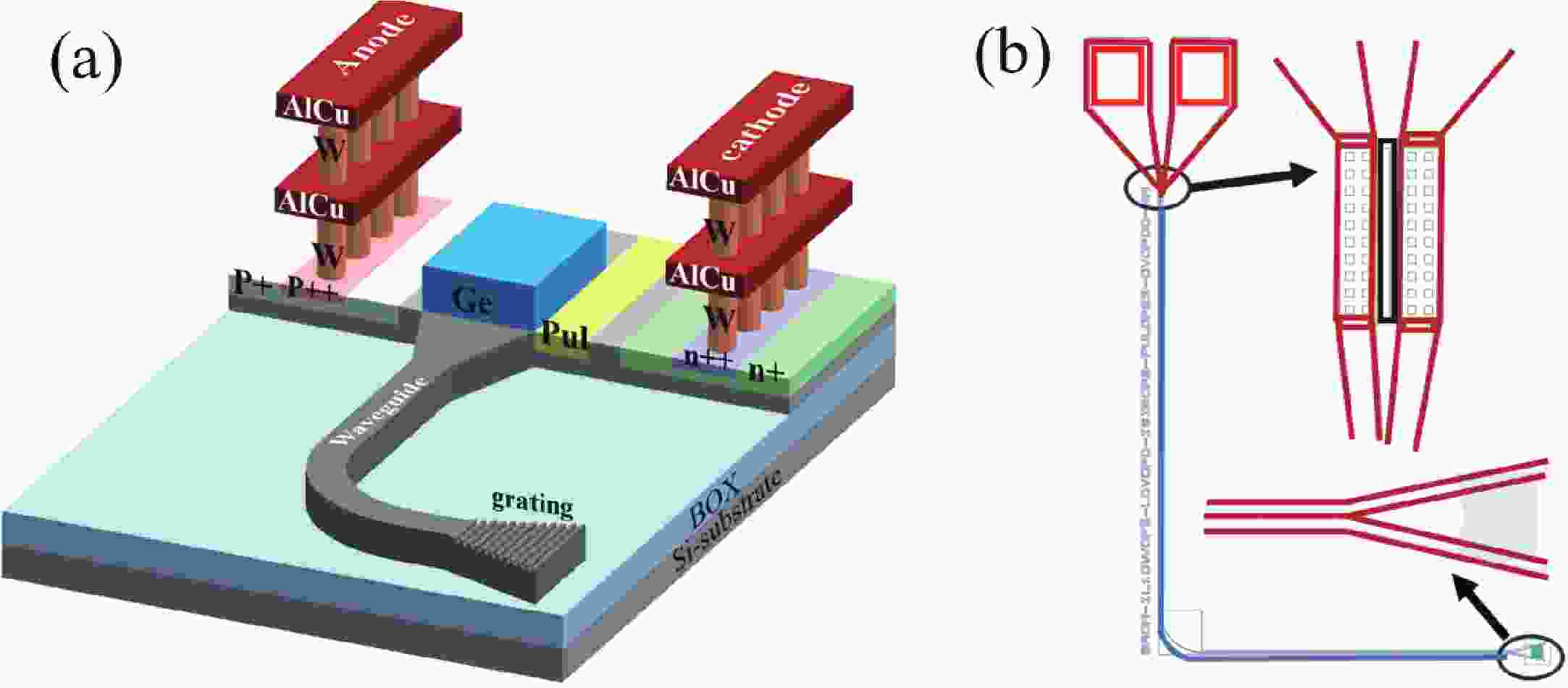
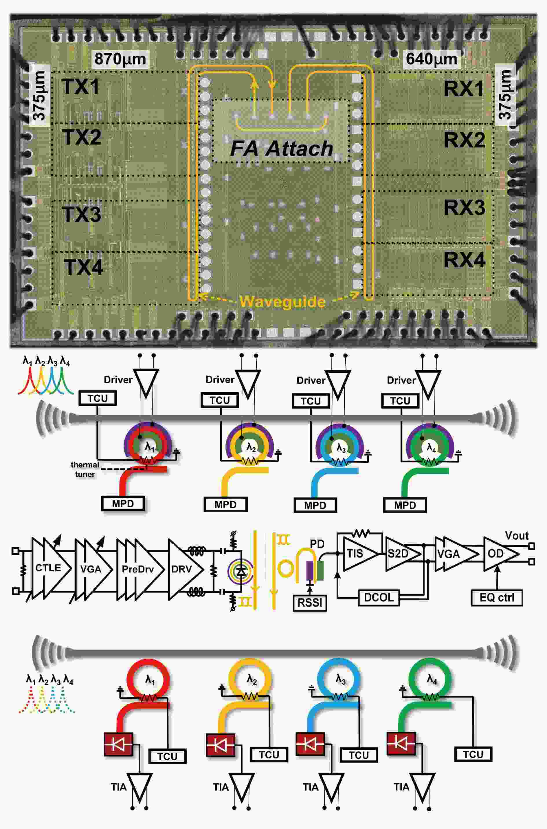
Avalanche photodetectors (APDs) featuring an avalanche multiplication region are vital for reaching high sensitivity and responsivity in optical transceivers. Waveguide-coupled Ge-on-Si separate absorption, charge, and multiplication (SACM) APDs are popular due to their straightforward fabrication process, low optical propagation loss, and high detection sensitivity in optical communications. This paper introduces a lateral SACM Ge-on-Si APD on a silicon-on-insulator (SOI) wafer, featuring a 10 μm-long, 0.5 μm-wide Ge layer at 1310 nm on a standard 8-inch silicon photonics platform. The dark current measures approximately 38.6 μA at −21 V, indicating a breakdown voltage greater than −21 V for the device. The APDs exhibit a unit-gain responsivity of 0.5 A/W at −10 V. At −15 V, their responsivity reaches 2.98 and 2.91 A/W with input powers of −10 and −25 dBm, respectively. The device's 3-dB bandwidth is 15 GHz with an input power of −15 dBm and a gain is 11.68. Experimental results show a peak in impedance at high bias voltages, attributed to inductor and capacitor (LC) circuit resonance, enhancing frequency response. Furthermore, 20 Gbps eye diagrams at −21 V and −9 dBm input power reveal signal to noise ratio (SNRs) of 5.30. This lateral SACM APD, compatible with the stand complementary metal oxide semiconductor (CMOS) process, shows that utilizing the peaking effect at low optical power increases bandwidth.
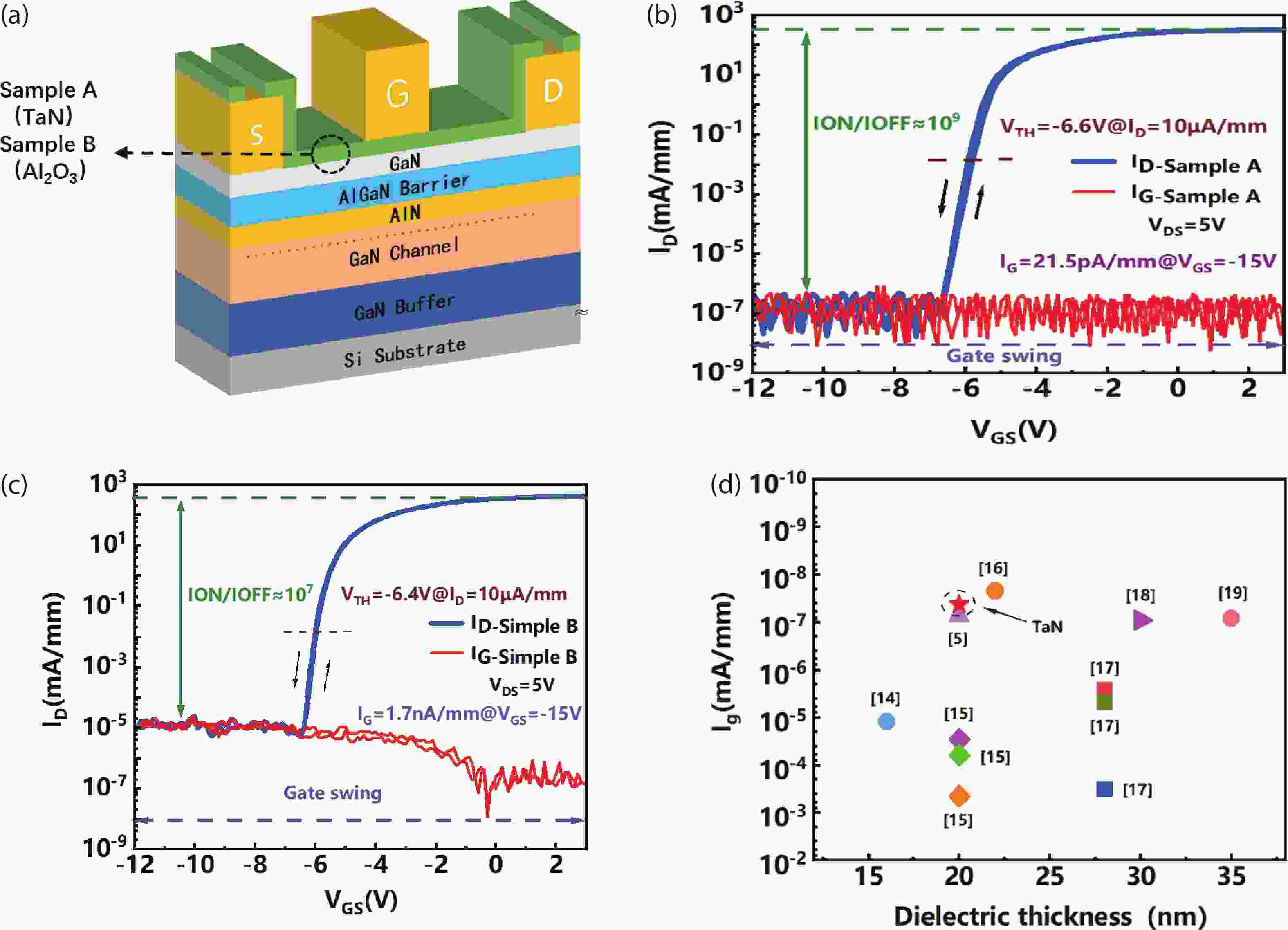
In this paper, we explore the electrical characteristics of high-electron-mobility transistors (HEMTs) using a TaN/AlGaN/GaN metal insulating semiconductor (MIS) structure. The high-resistance tantalum nitride (TaN) film prepared by magnetron sputtering as the gate dielectric layer of the device achieved an effective reduction of electronic states at the TaN/AlGaN interface, and reducing the gate leakage current of the MIS HEMT, its performance was enhanced. The HEMT exhibited a low gate leakage current of 2.15 × 10⁻⁷ mA/mm and a breakdown voltage of 1180 V. Furthermore, the MIS HEMT displayed exceptional operational stability during dynamic tests, with dynamic resistance remaining only 1.39 times even under 400 V stress.
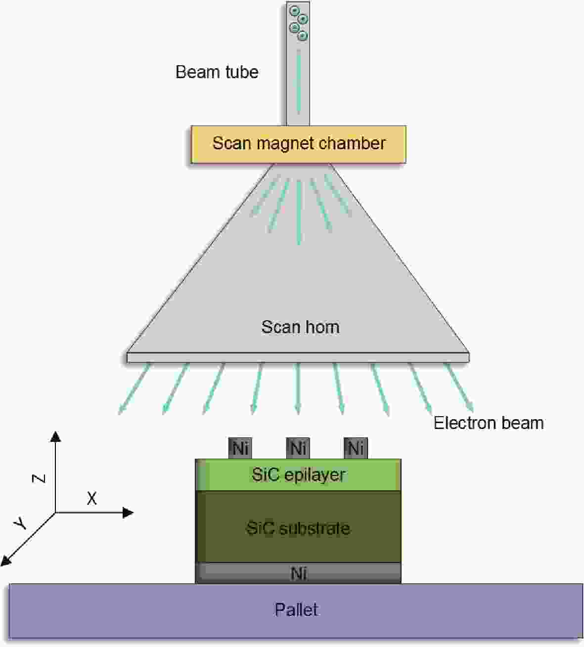
Radiation damage produced in 4H-SiC by electrons of different doses is presented by using multiple characterization techniques. Raman spectra results indicate that SiC crystal structures are essentially impervious to 10 MeV electron irradiation with doses up to 3000 kGy. However, irradiation indeed leads to the generation of various defects, which are evaluated through photoluminescence (PL) and deep level transient spectroscopy (DLTS). The PL spectra feature a prominent broad band centered at 500 nm, accompanied by several smaller peaks ranging from 660 to 808 nm. The intensity of each PL peak demonstrates a linear correlation with the irradiation dose, indicating a proportional increase in defect concentration during irradiation. The DLTS spectra reveal several thermally unstable and stable defects that exhibit similarities at low irradiation doses. Notably, after irradiating at the higher dose of 1000 kGy, a new stable defect labeled as R2 (Ec − 0.51 eV) appeared after annealing at 800 K. Furthermore, the impact of irradiation-induced defects on SiC junction barrier Schottky diodes is discussed. It is observed that high-dose electron irradiation converts SiC n-epilayers to semi-insulating layers. However, subjecting the samples to a temperature of only 800 K results in a significant reduction in resistance due to the annealing out of unstable defects.
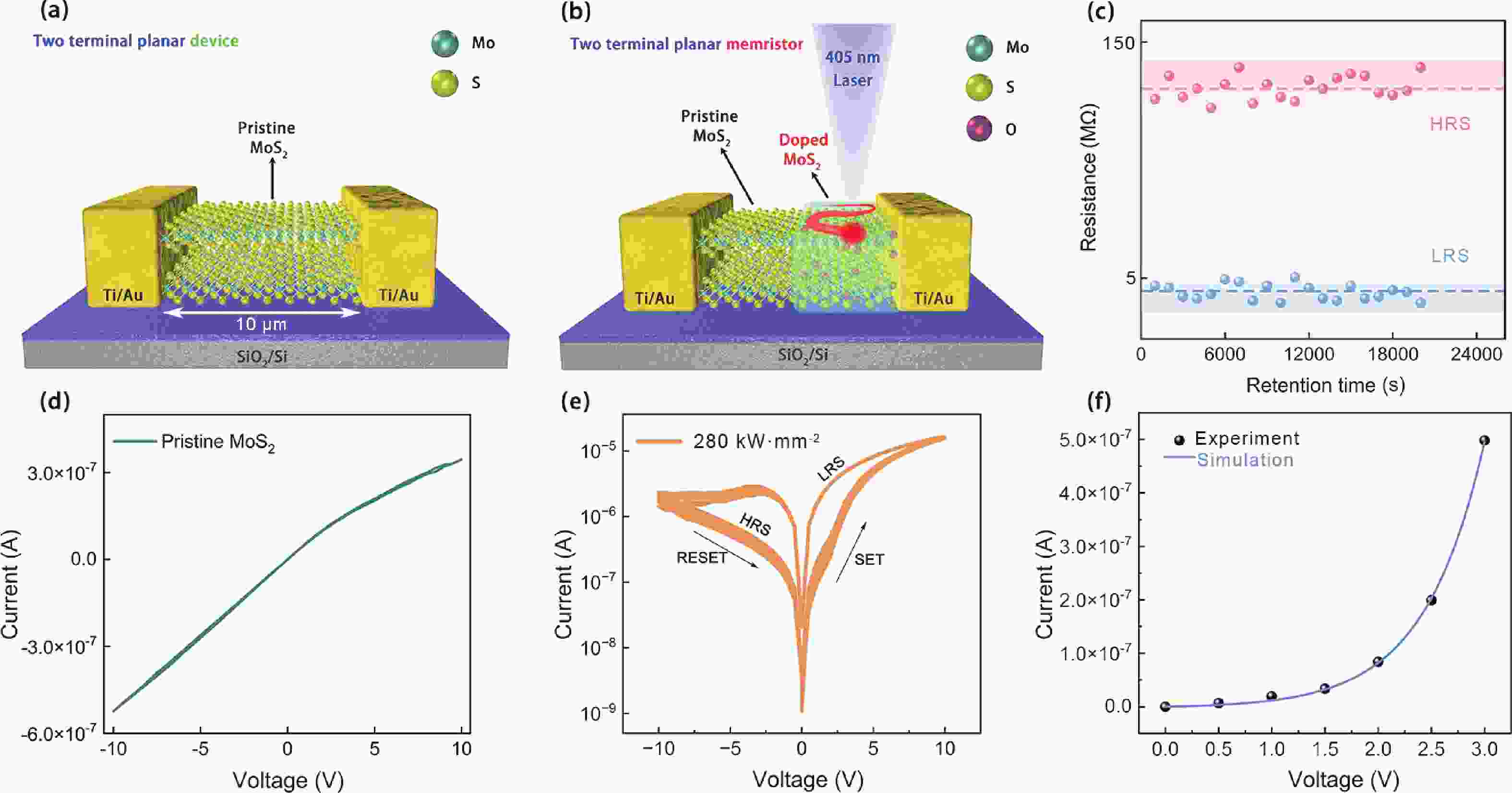
Memristors as non-volatile memory devices have gained numerous attentions owing to their advantages in storage, in-memory computing, synaptic applications, etc. In recent years, two-dimensional (2D) materials with moderate defects have been discovered to exist memristive feature. However, it is very difficult to obtain moderate defect degree in 2D materials, and studied on modulation means and mechanism becomes urgent and essential. In this work, we realized memristive feature with a bipolar switching and a configurable on/off ratio in a two-terminal MoS2 device (on/off ratio ~100), for the first time, from absent to present using laser-modulation to few-layer defect-free MoS2 (about 10 layers), and its retention time in both high resistance state and low resistance state can reach 2 × 10⁴ s. The mechanism of the laser-induced memristive feature has been cleared by dynamic Monte Carlo simulations and first-principles calculations. Furthermore, we verified the universality of the laser-modulation by investigating other 2D materials of TMDs. Our work will open a route to modulate and optimize the performance of 2D semiconductor memristive devices.


