Issue Browser
Volume 46, Issue 8,
Aug 2025
Column
J. Semicond.
2025, 46(8): 081401 doi: 10.1088/1674-4926/25010010

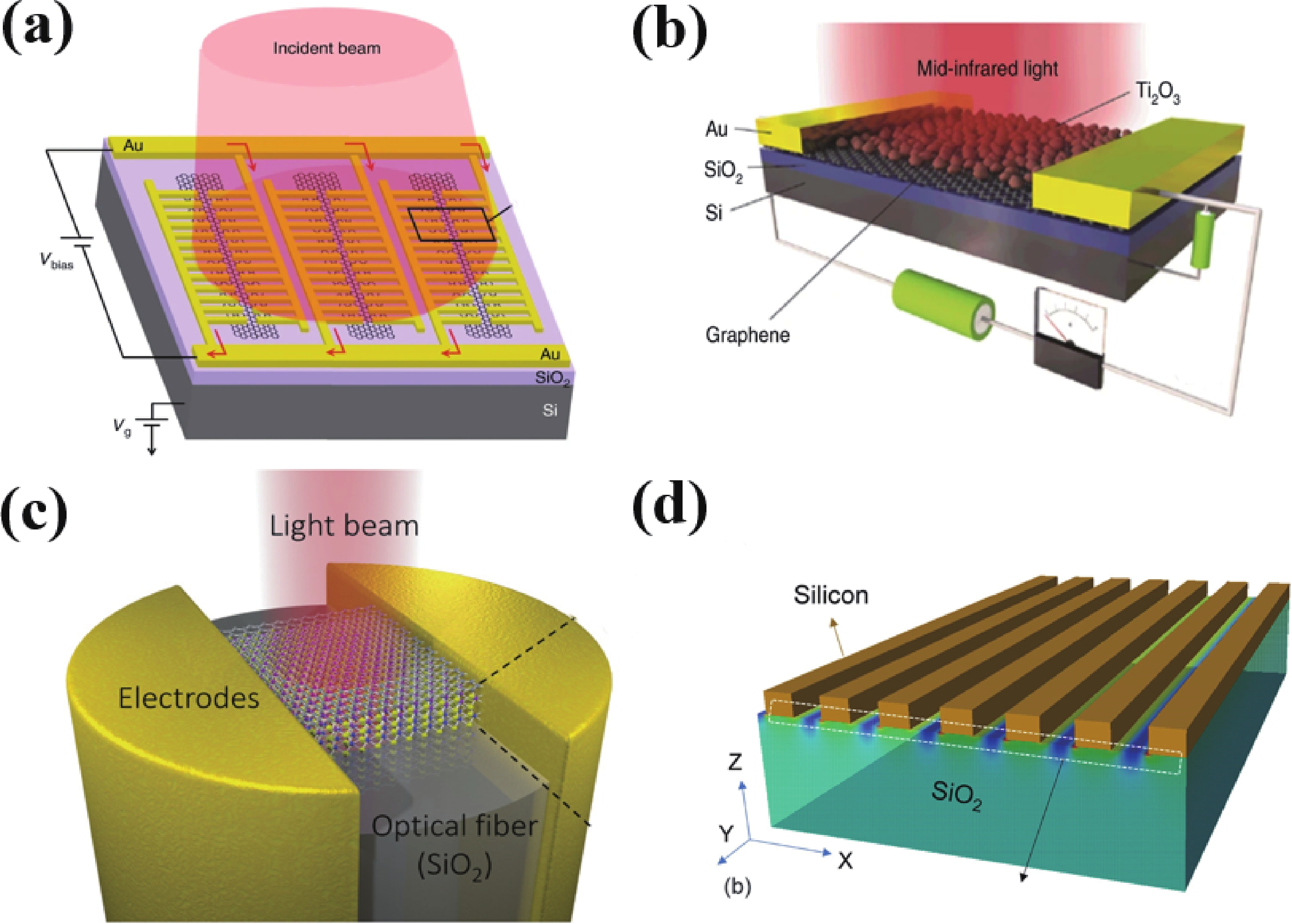
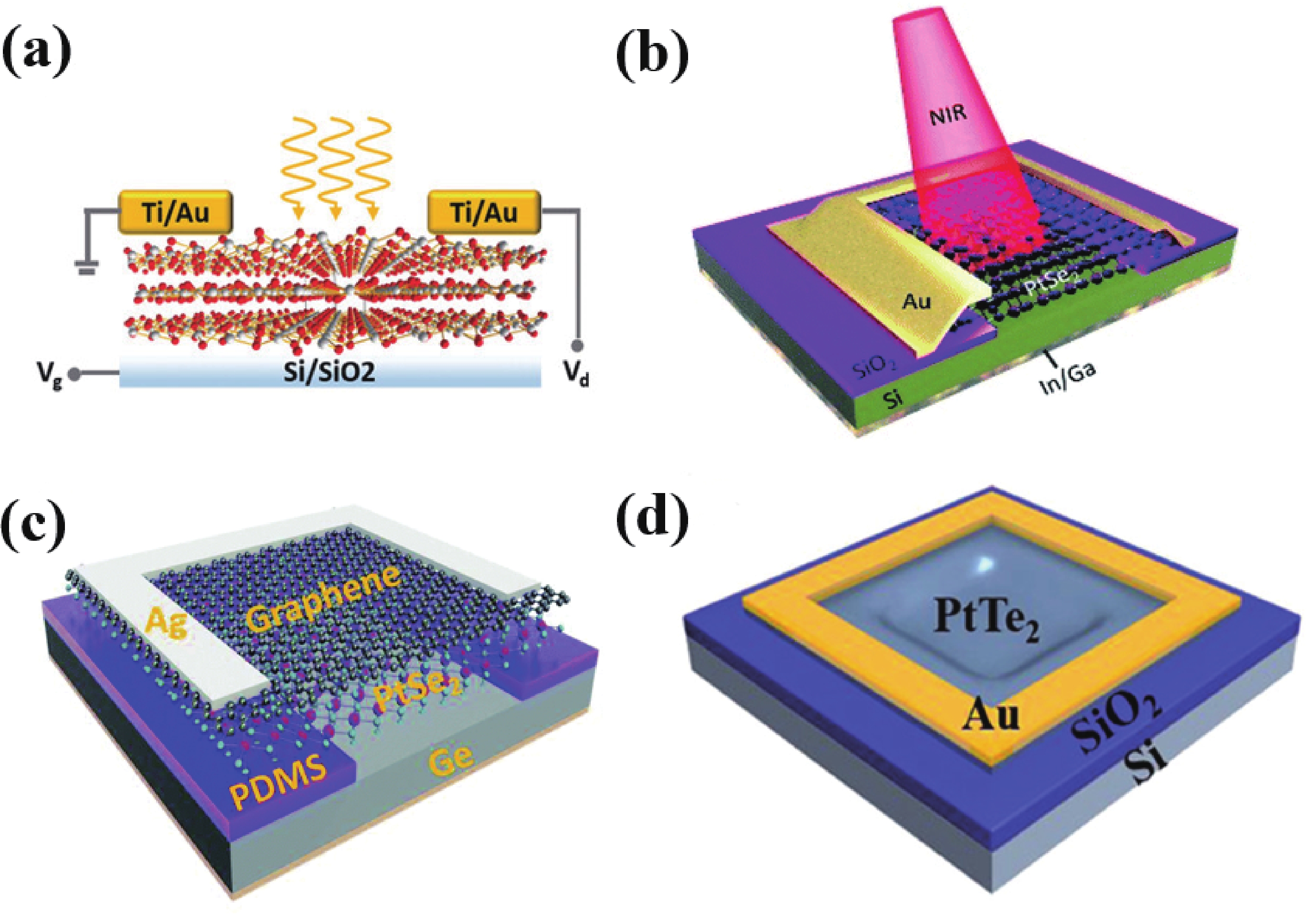
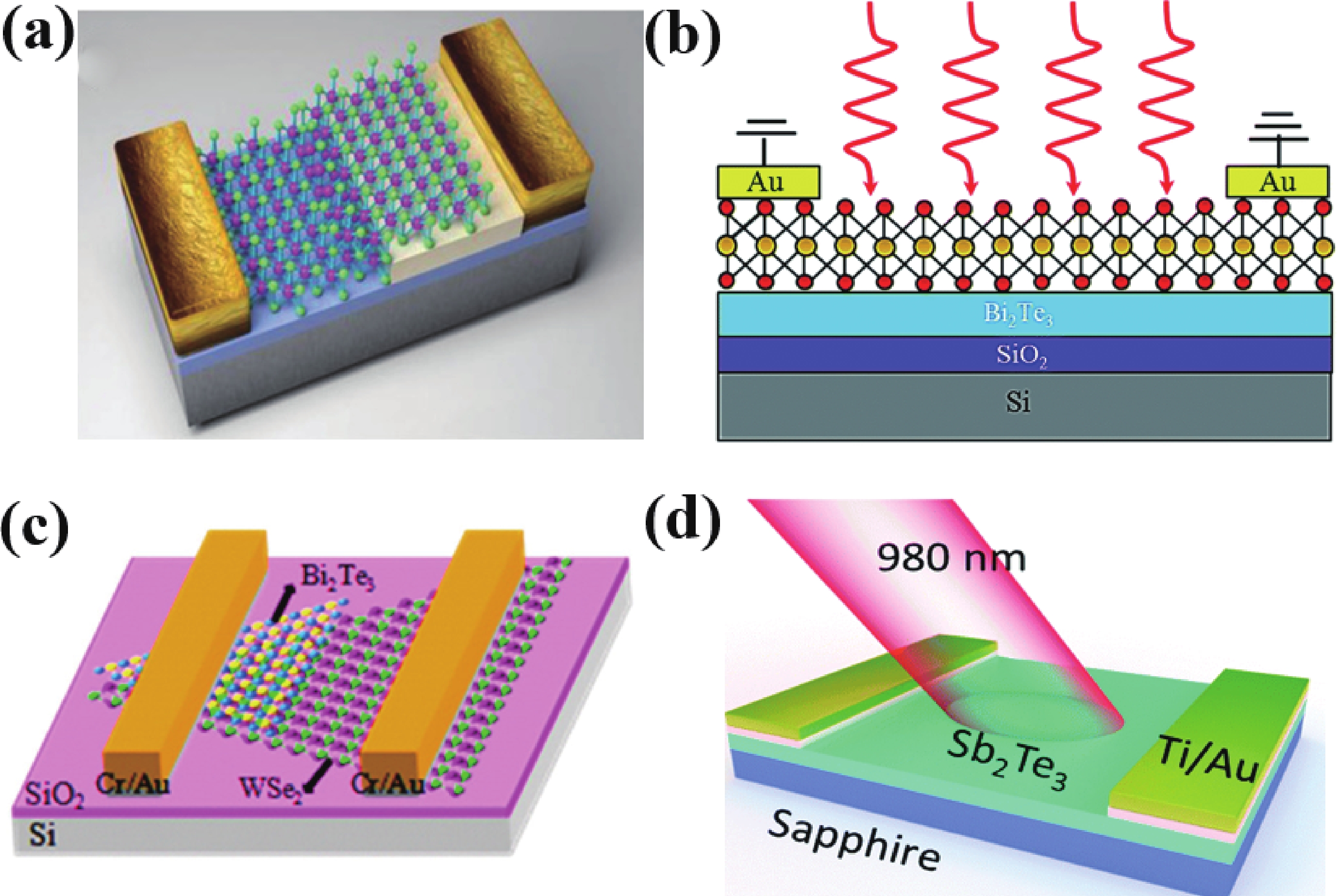
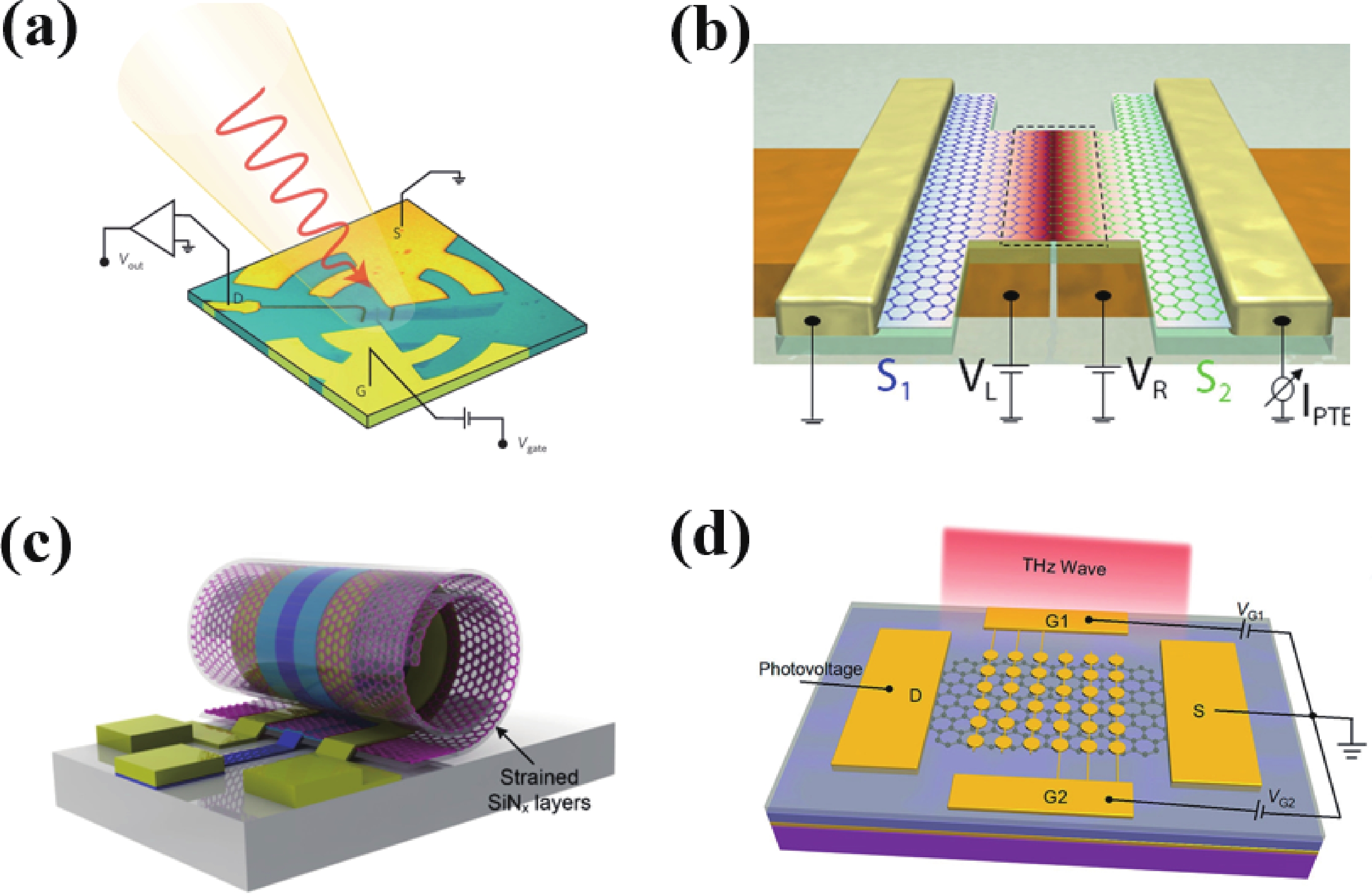
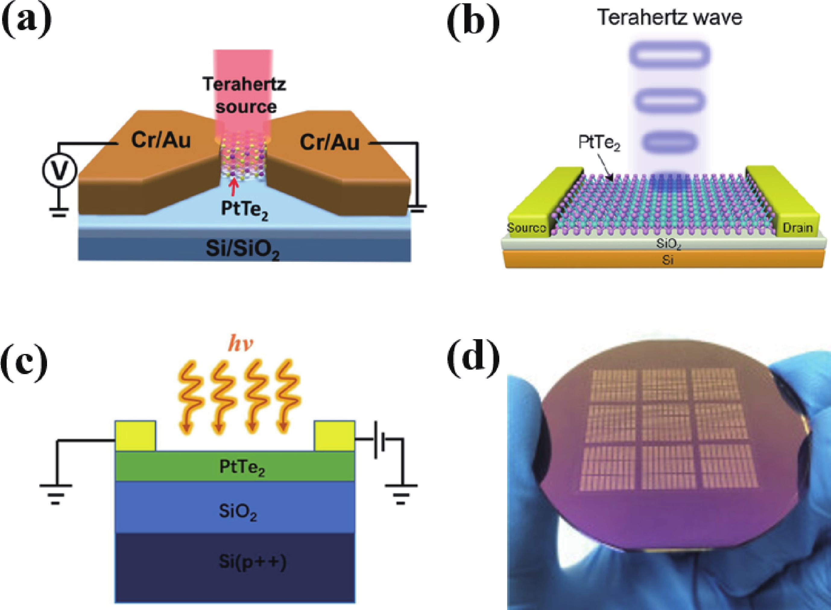
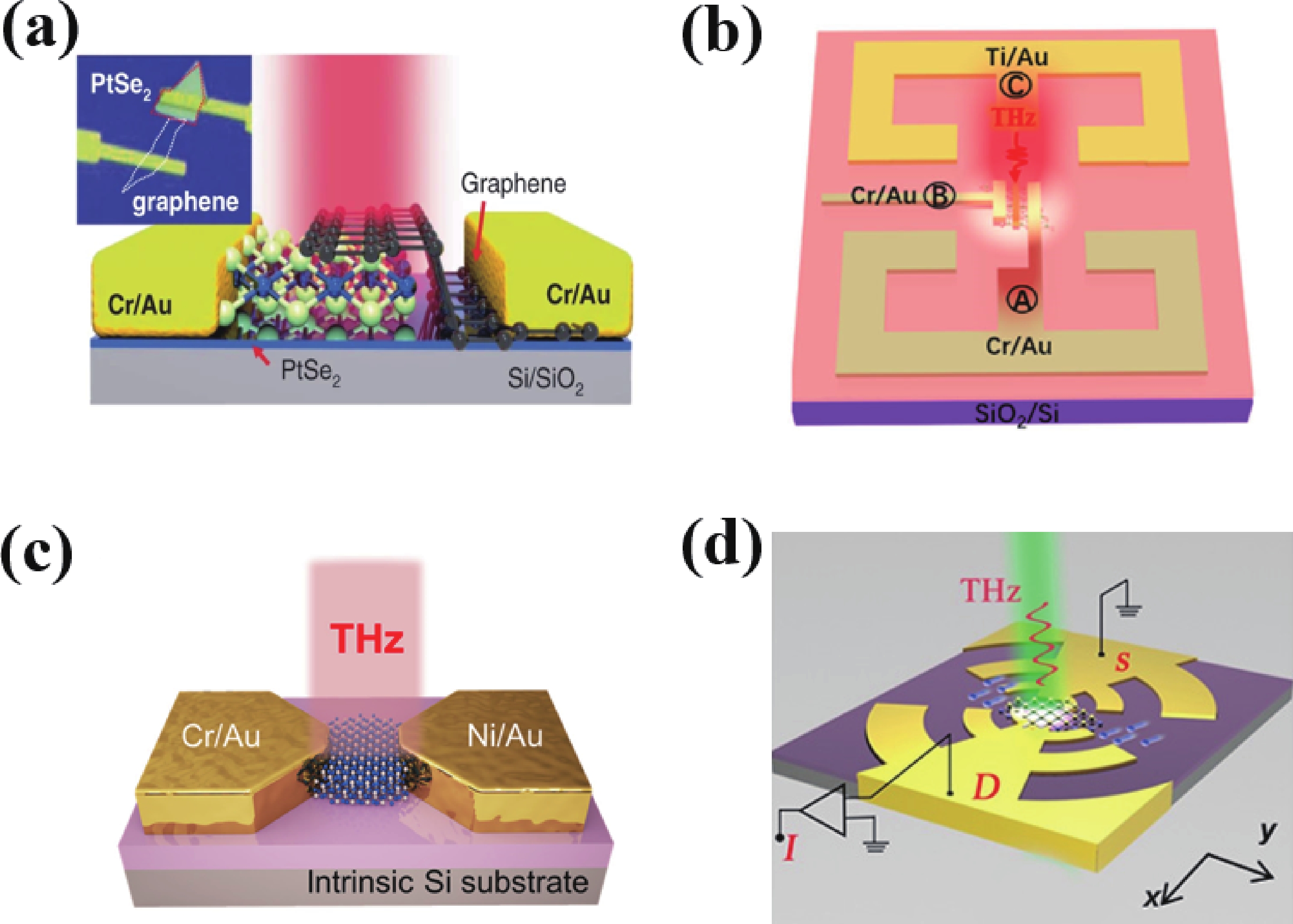
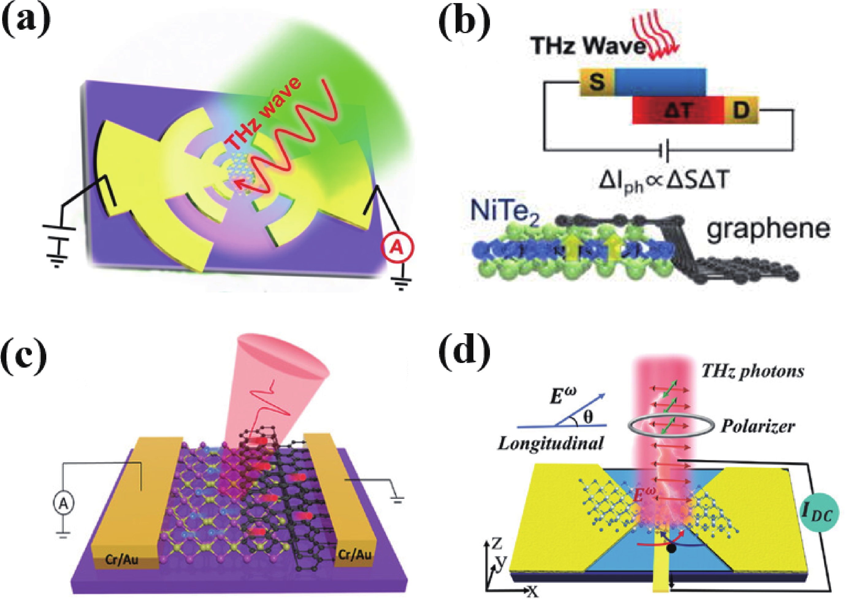
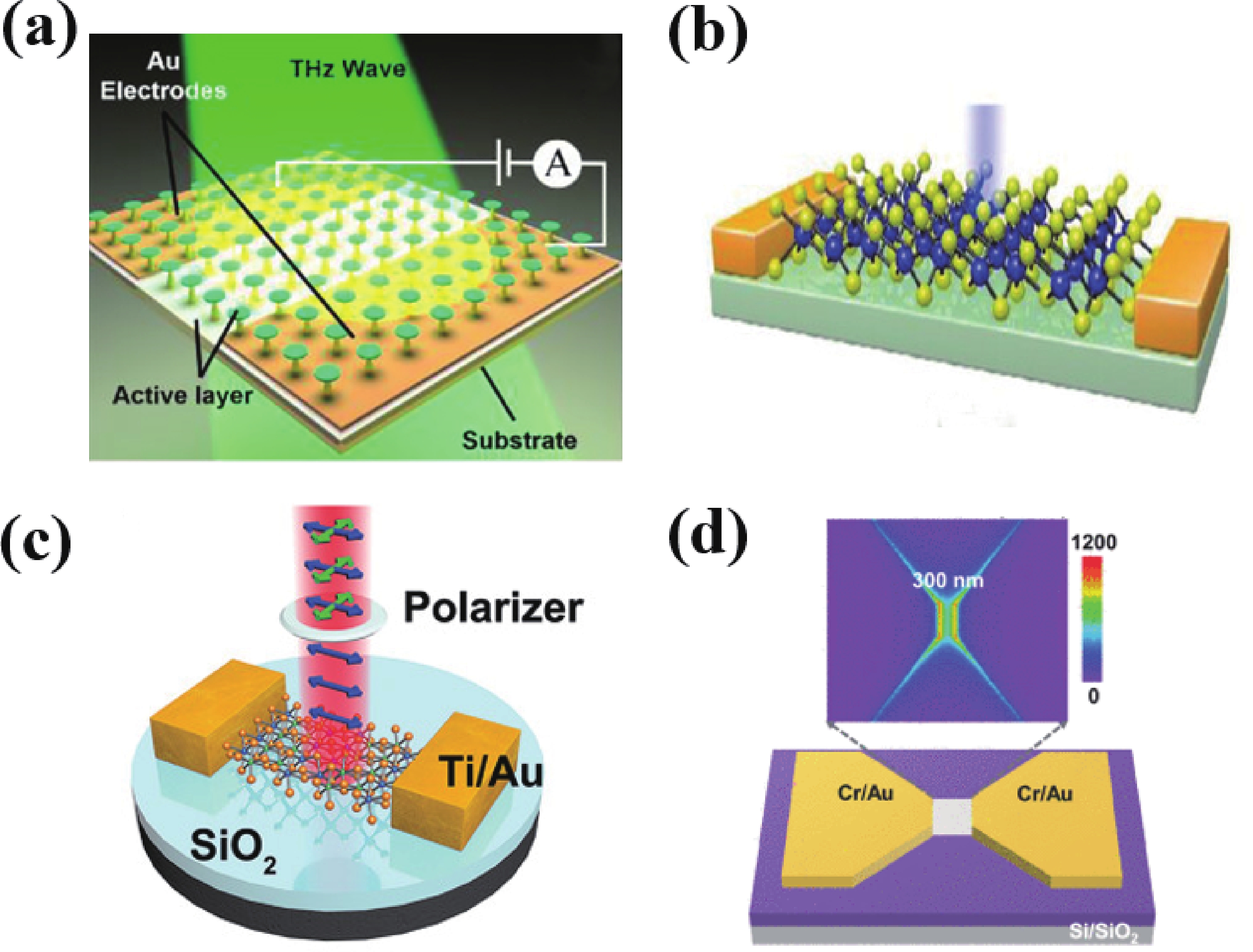
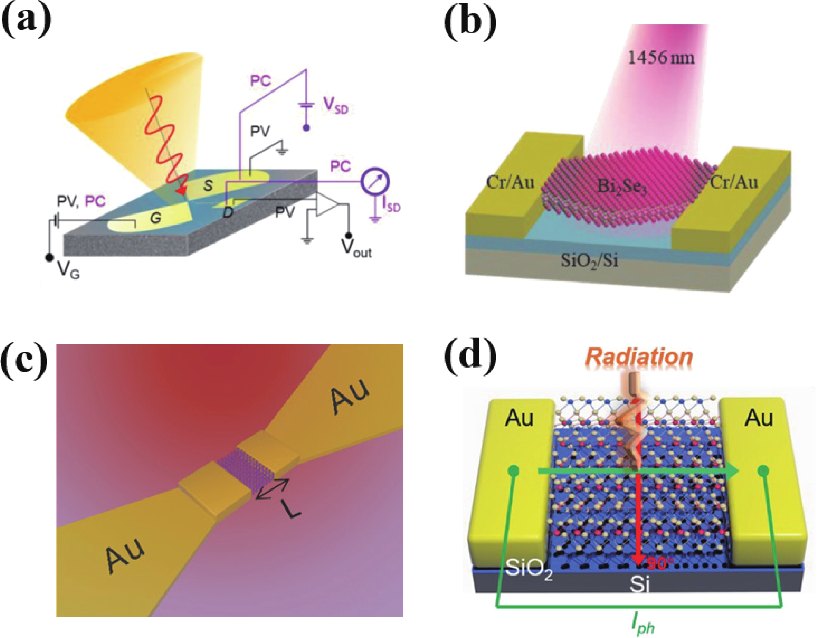
Infrared and terahertz waves constitute pivotal bands within the electromagnetic spectrum, distinguished by their robust penetration capabilities and non-ionizing nature. These wavebands offer the potential for achieving high-resolution and non-destructive detection methodologies, thereby possessing considerable research significance across diverse domains including communication technologies, biomedical applications, and security screening systems. Two-dimensional materials, owing to their distinctive optoelectronic attributes, have found widespread application in photodetection endeavors. Nonetheless, their efficacy diminishes when tasked with detecting lower photon energies. Furthermore, as the landscape of device integration evolves, two-dimensional materials struggle to align with the stringent demands for device superior performance. Topological materials, with their topologically protected electronic states and non-trivial topological invariants, exhibit quantum anomalous Hall effects and ultra-high carrier mobility, providing a new approach for seeking photosensitive materials for infrared and terahertz photodetectors. This article introduces various types of topological materials and their properties, followed by an explanation of the detection mechanism and performance parameters of photodetectors. Finally, it summarizes the current research status of near-infrared to far-infrared photodetectors and terahertz photodetectors based on topological materials, discussing the challenges faced and future prospects in their development.
J. Semicond.
2025, 46(8): 082201 doi: 10.1088/1674-4926/24120039
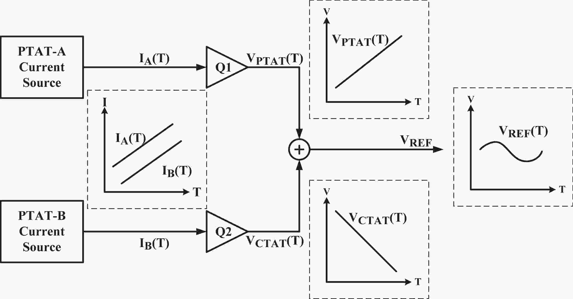
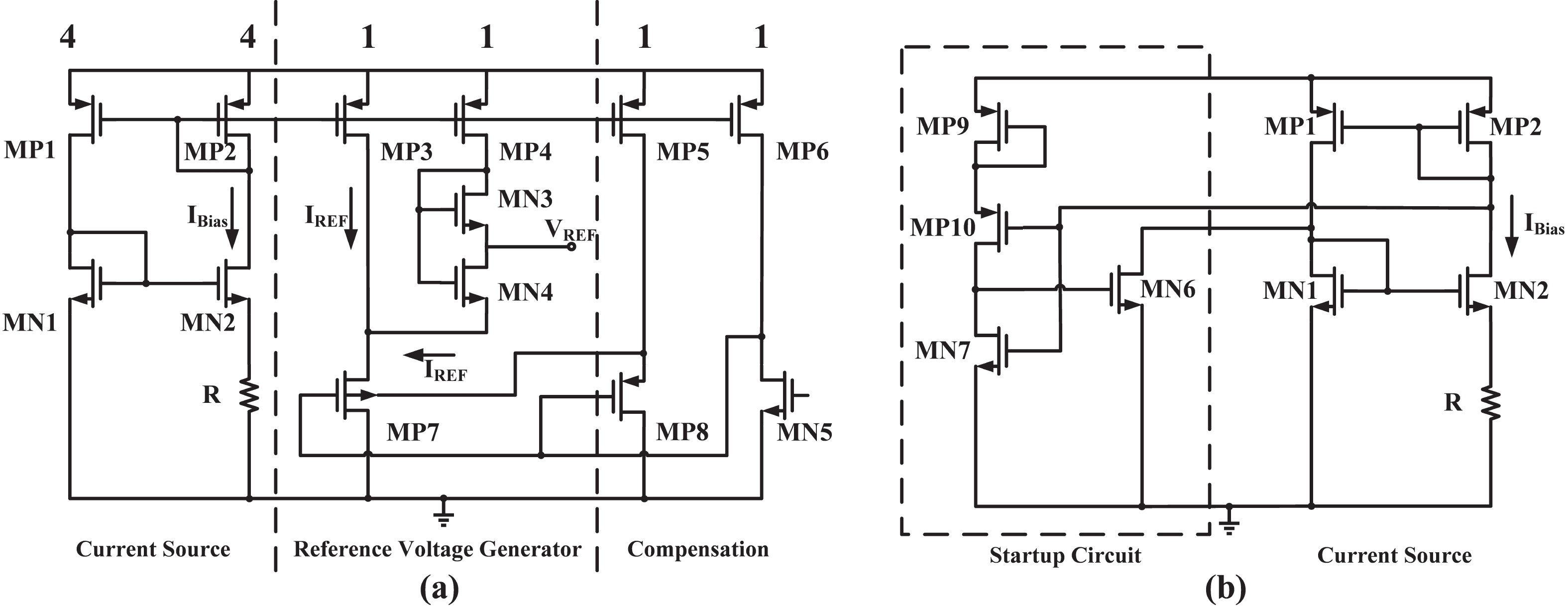
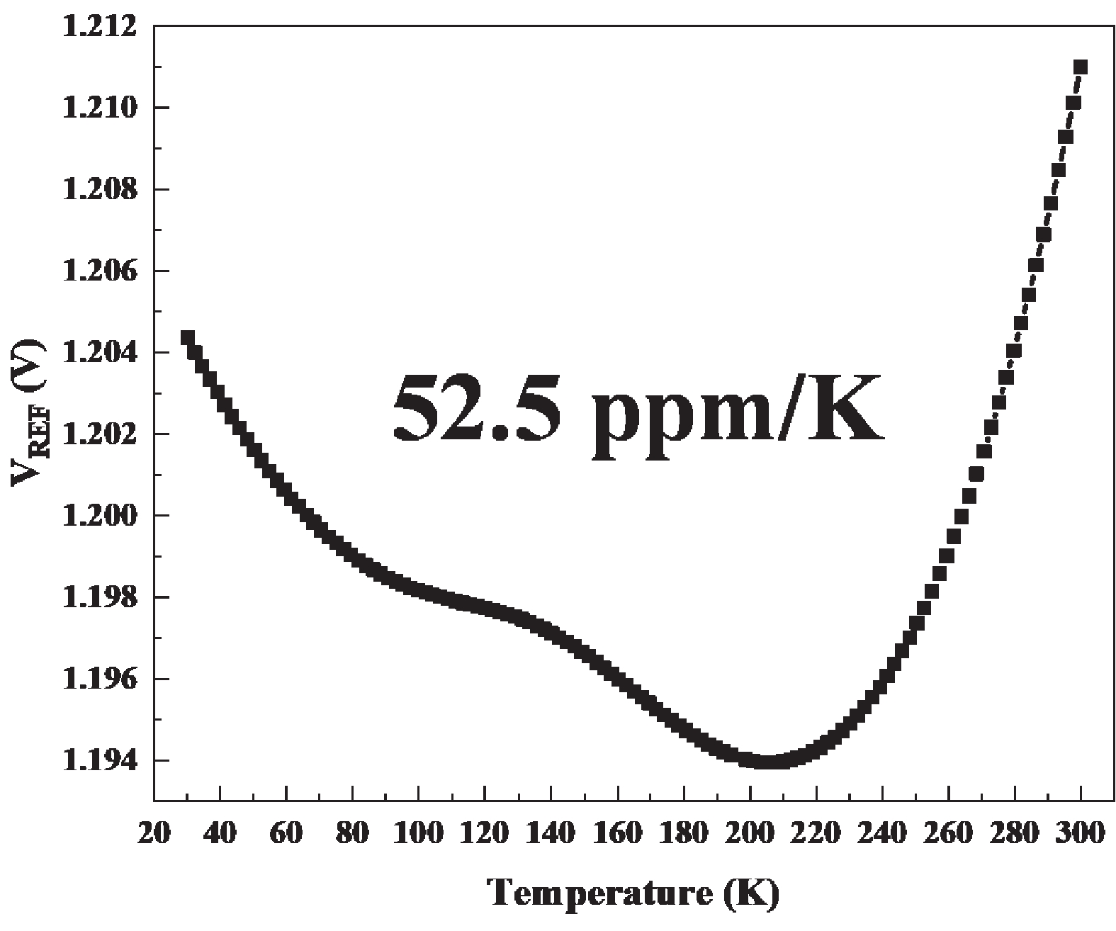
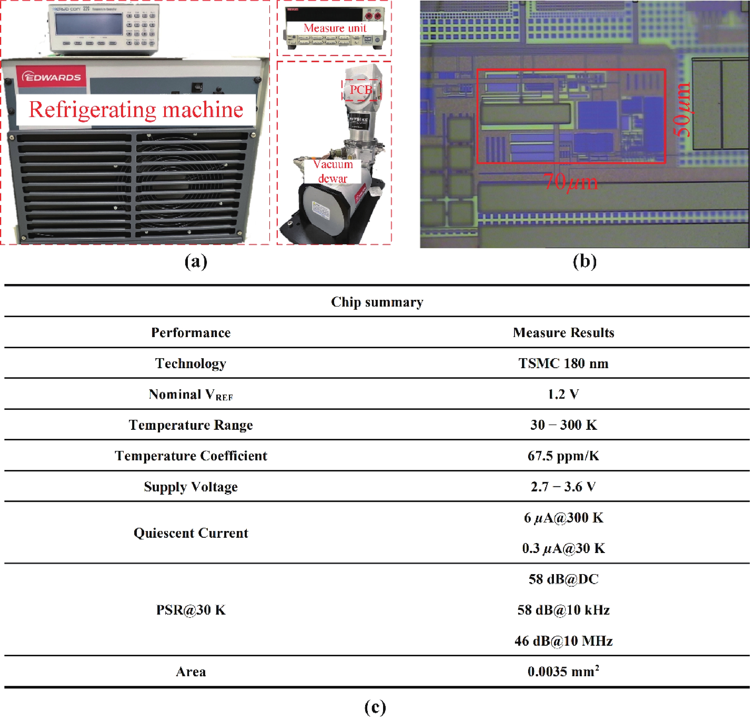
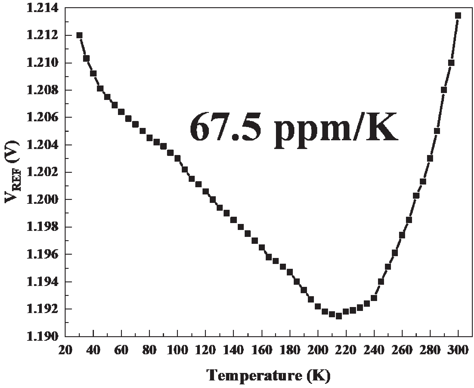
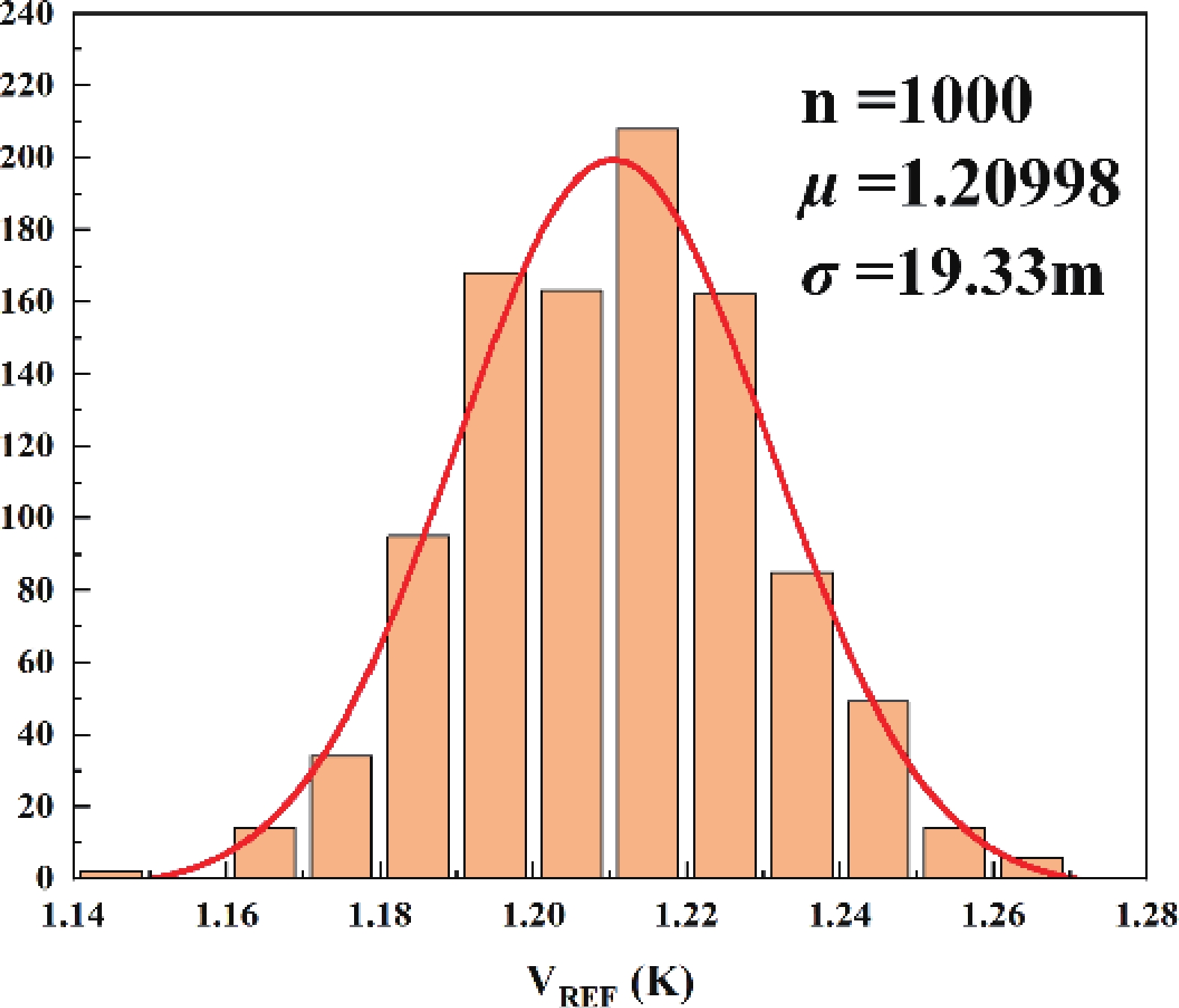
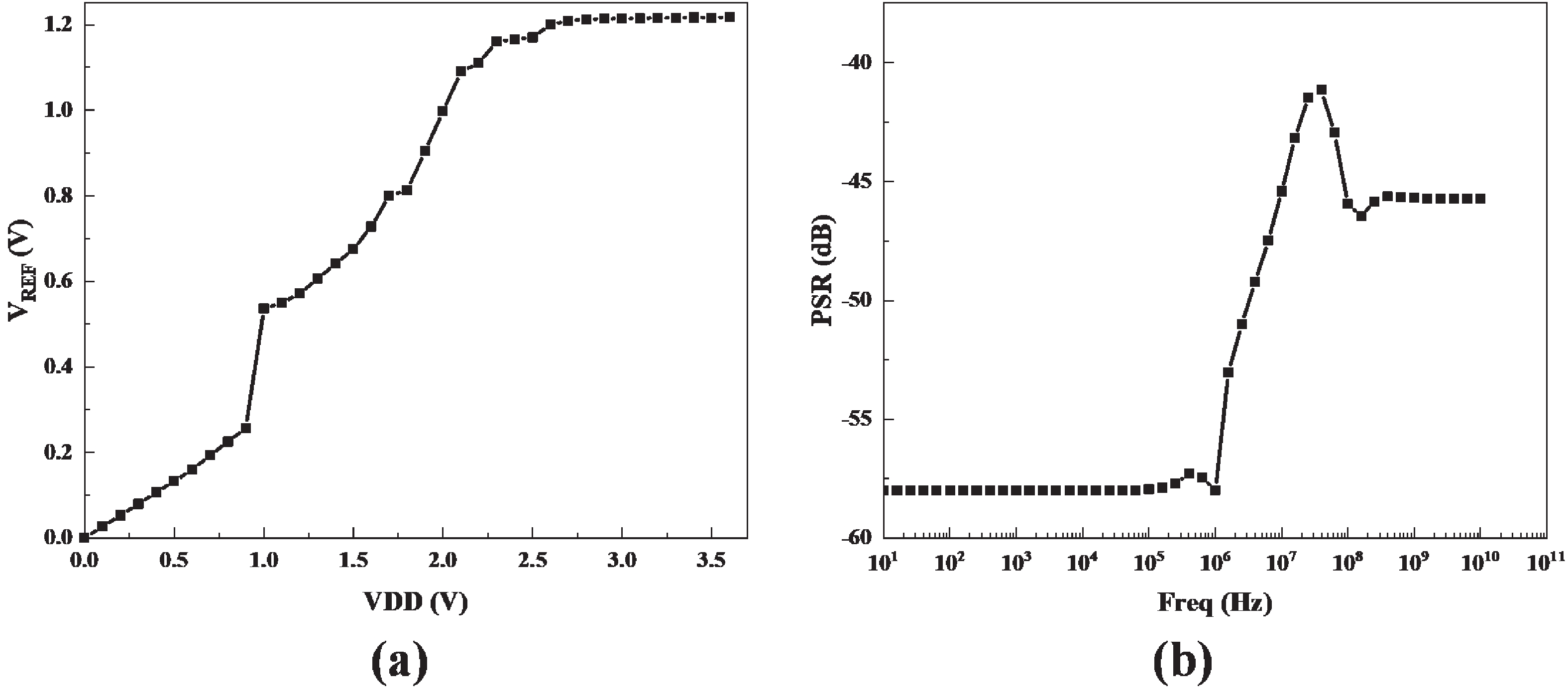
This brief presents a cryogenic voltage reference circuit designed to operate effectively across a wide temperature range from 30 to 300 K. A key feature of the proposed design is utilizing a current subtraction technique for temperature compensation of the reference current, avoiding the deployment of bipolar transistors to reduce area and power consumption. Implemented with a 0.18-µm CMOS process, the circuit achieves a temperature coefficient (TC) of 67.5 ppm/K, which was not achieved in previous works. The design can also attain a power supply rejection (PSR) of 58 dB at 10 kHz. Meanwhile, the average reference voltage is 1.2 V within a 1.6% 3σ-accuracy spread. Additionally, the design is characterized by a minimal power dissipation of 1 µW at 30 K and a compact chip area of 0.0035 mm².
J. Semicond.
2025, 46(8): 082202 doi: 10.1088/1674-4926/24110028

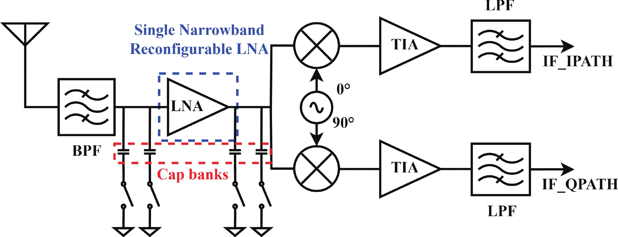
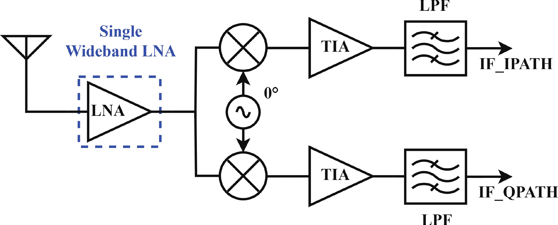
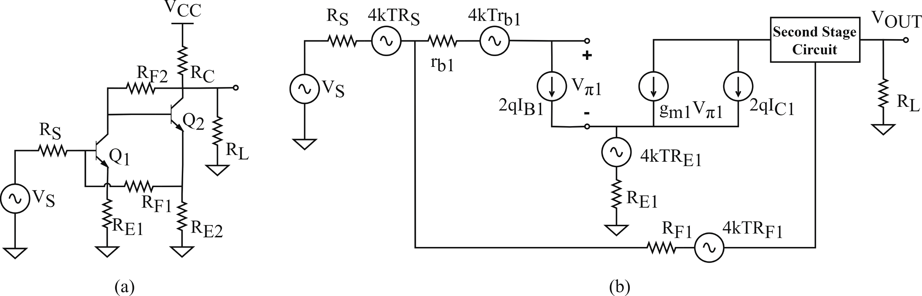
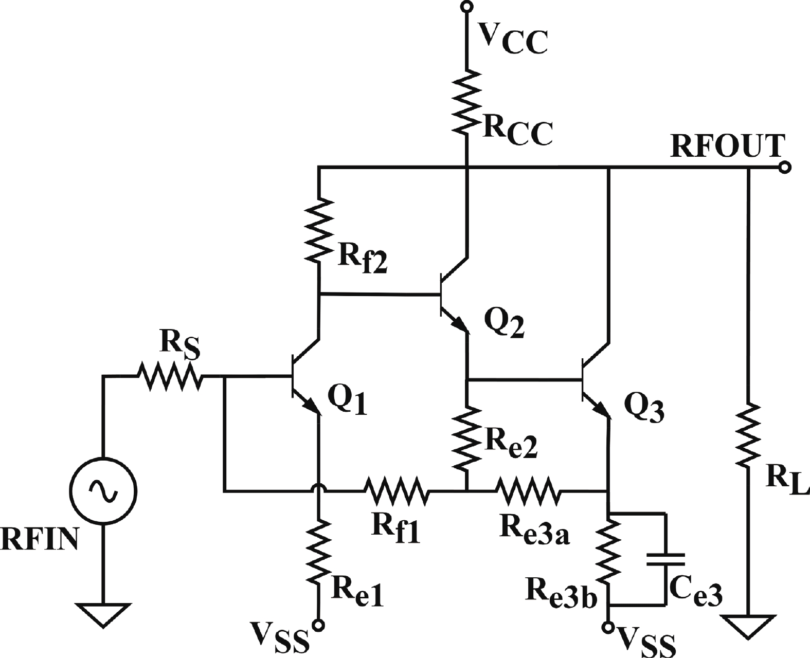
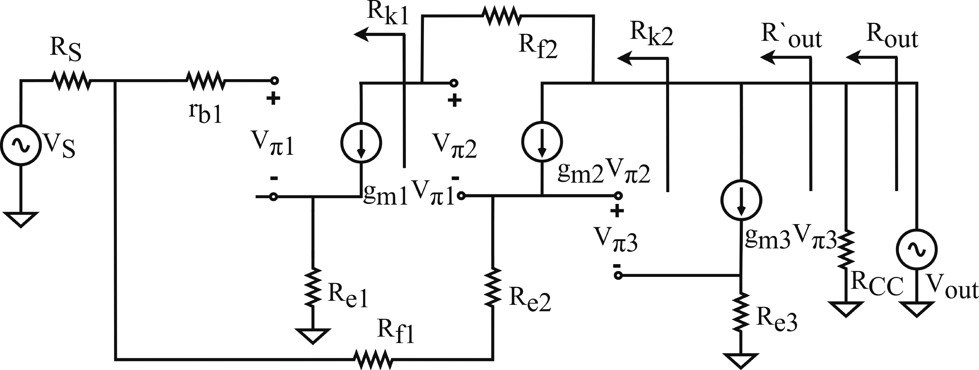
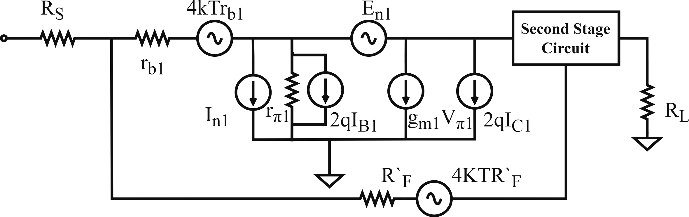
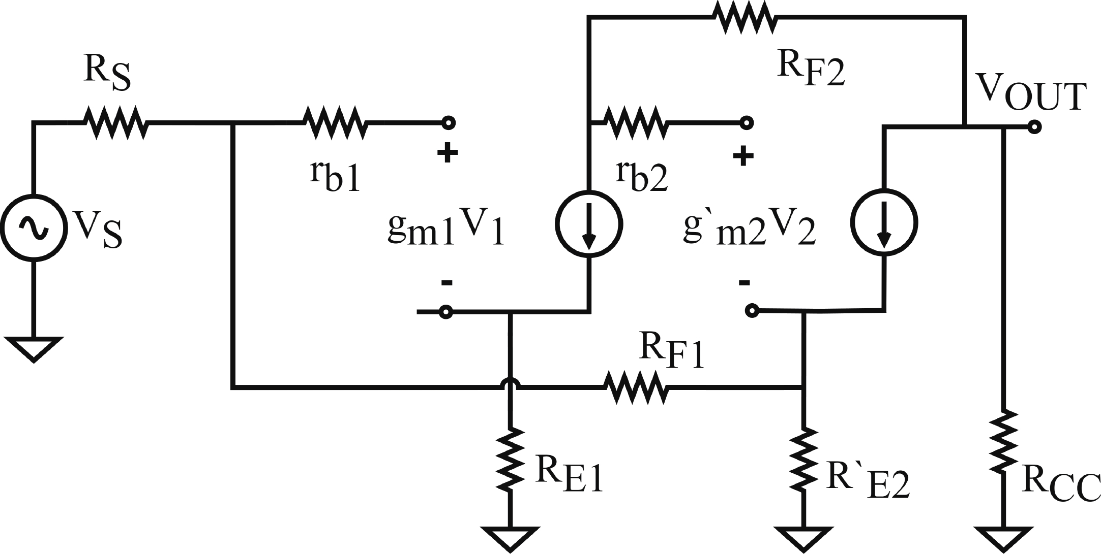
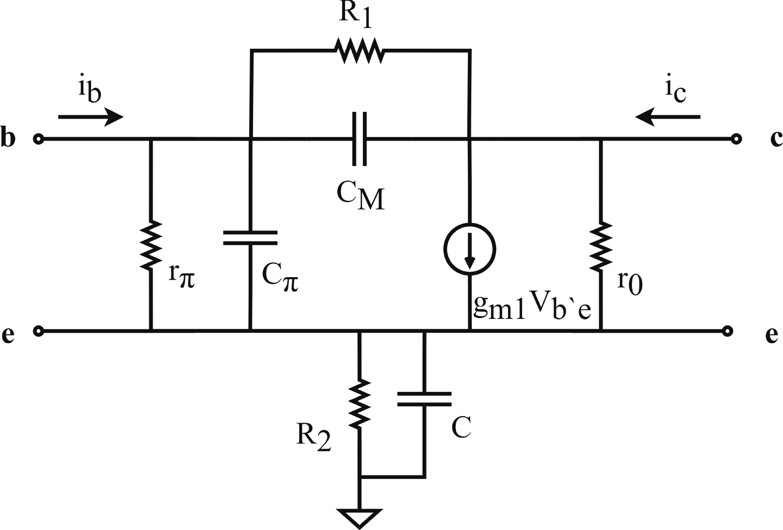
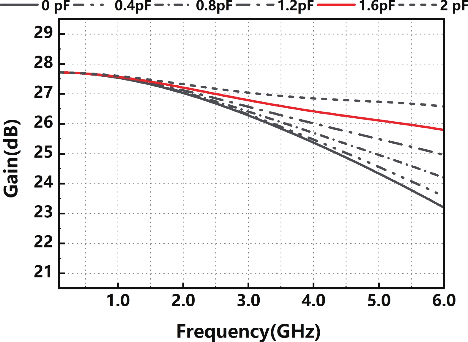
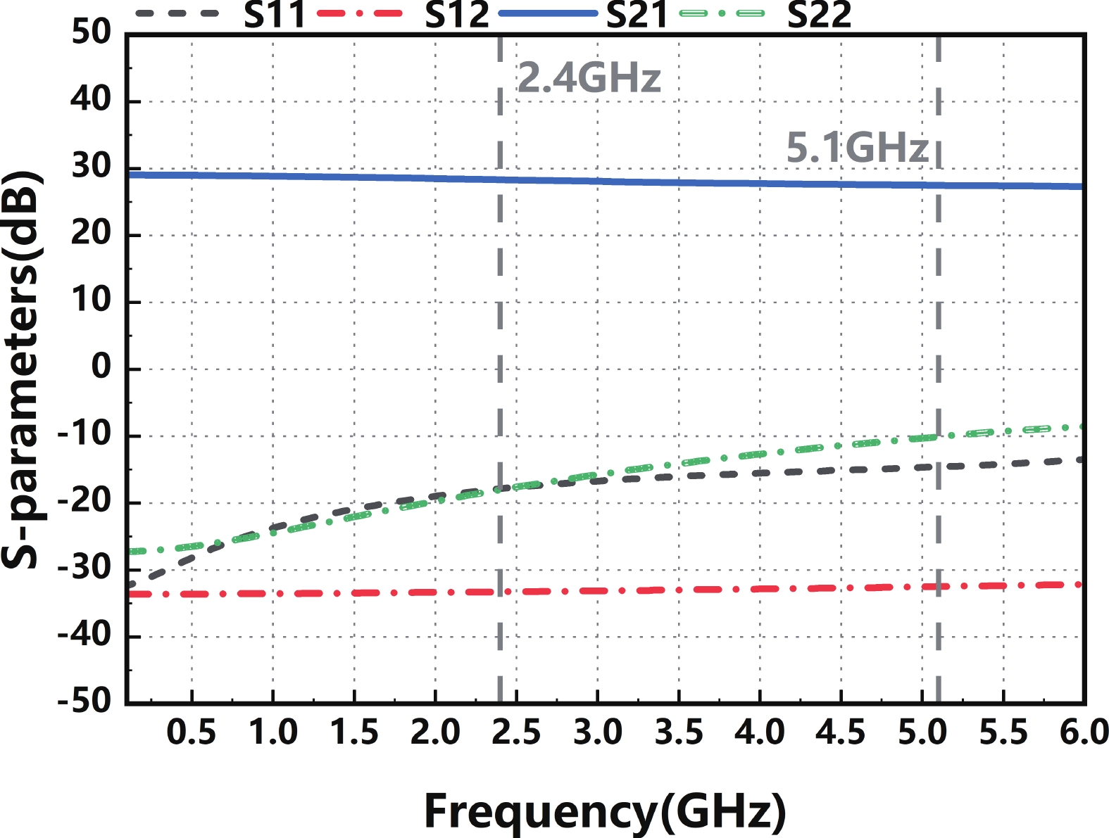
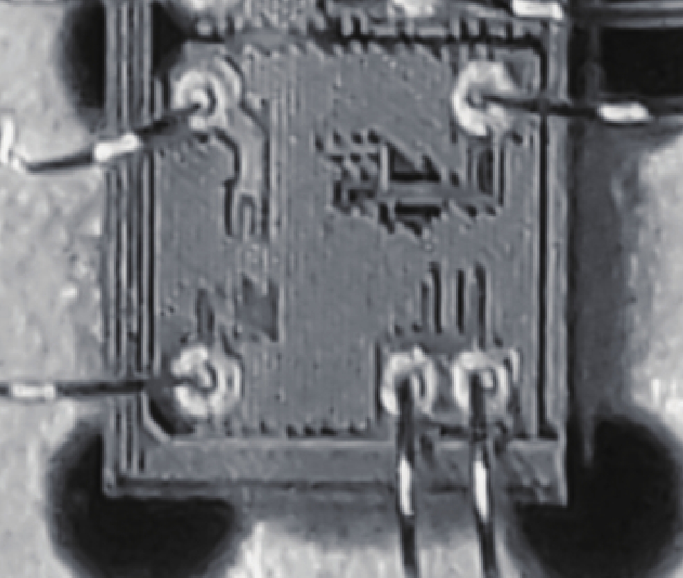
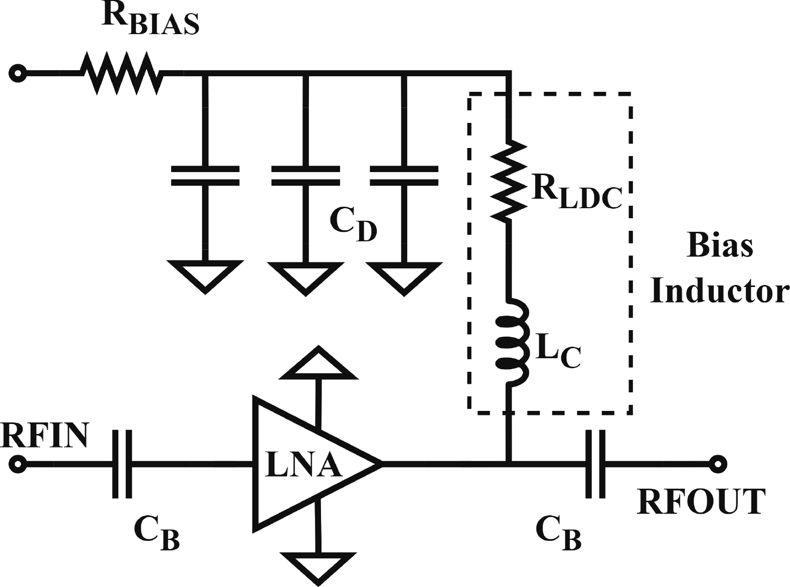
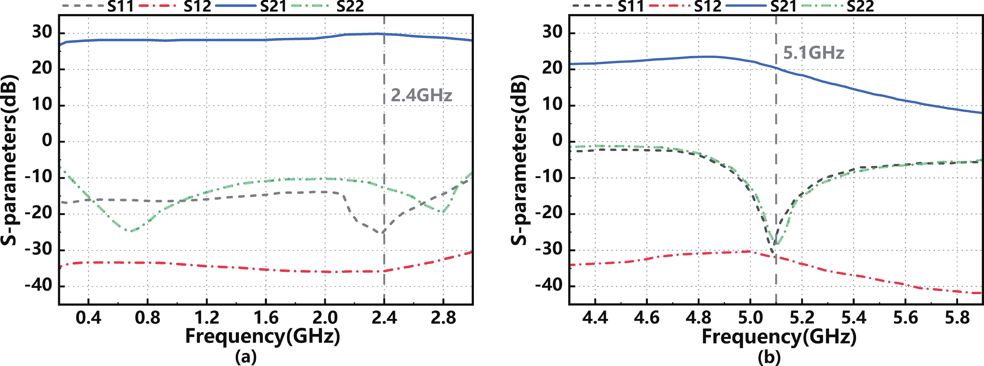
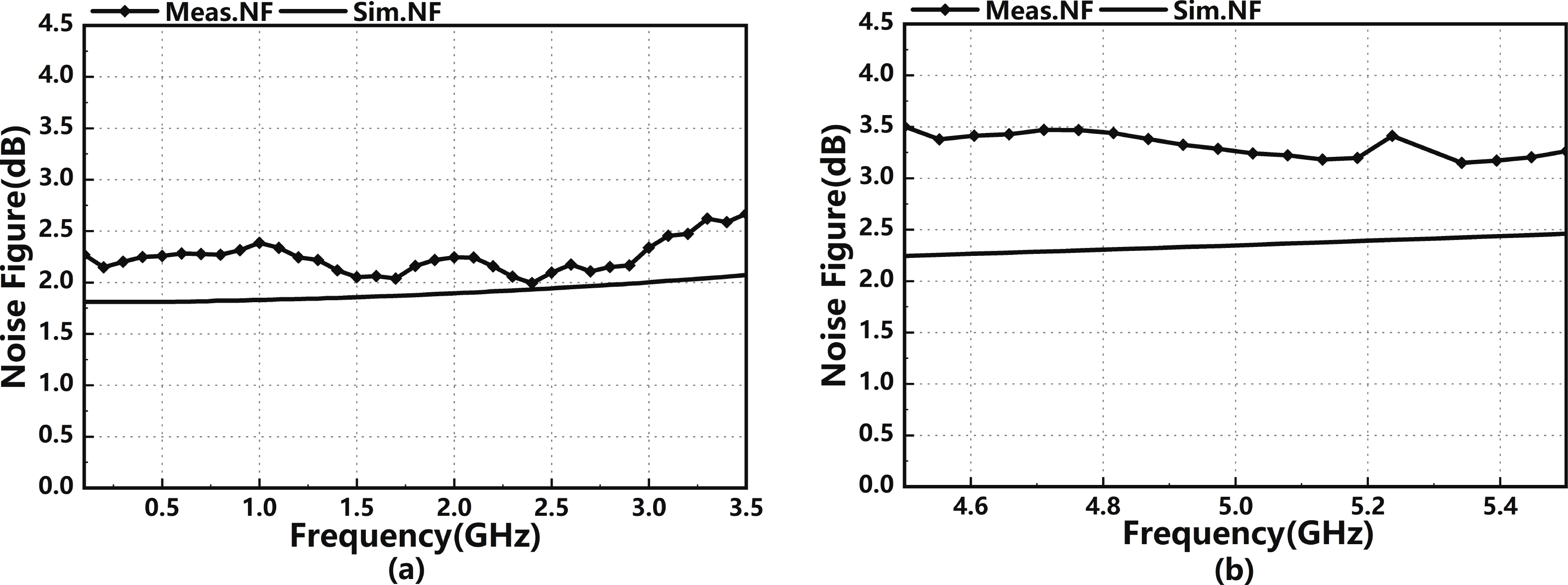
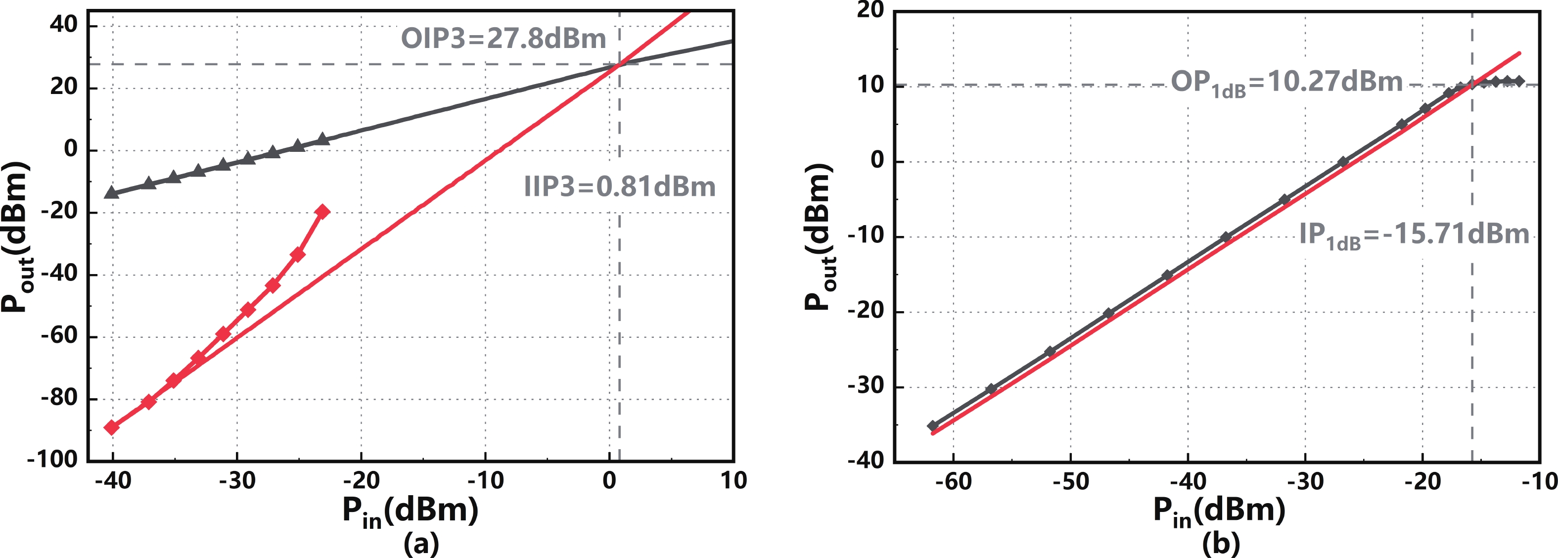
In this paper, a high-gain inductorless LNA (low-noise amplifier) compatible with multiple communication protocols from 0.1 to 5.1 GHz is proposed. A composite resistor−capacitor feedback structure is employed to achieve a wide bandwidth matching range and good gain flatness. A second stage with a Darlington pair is used to increase the overall gain of the amplifier, while the gain of the first stage is reduced to reduce the overall noise. The amplifier is based on a 0.25 μm SiGe BiCMOS process, and thanks to the inductorless circuit structure, the core circuit area is only 0.03 mm2. Test results show that the lowest noise figure (NF) in the operating band is 1.99 dB, the power gain reaches 29.7 dB, the S11 and S22 are less than −10 dB, the S12 is less than −30 dB, the IIP3 is 0.81dBm, and the OP1dB is 10.27 dBm. The operating current is 31.18 mA at 3.8 V supply.
J. Semicond.
2025, 46(8): 082301 doi: 10.1088/1674-4926/24120005
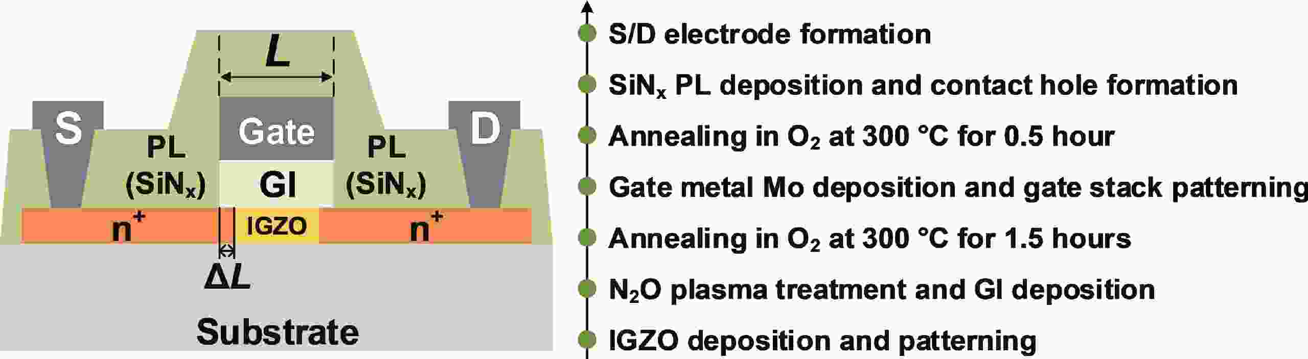
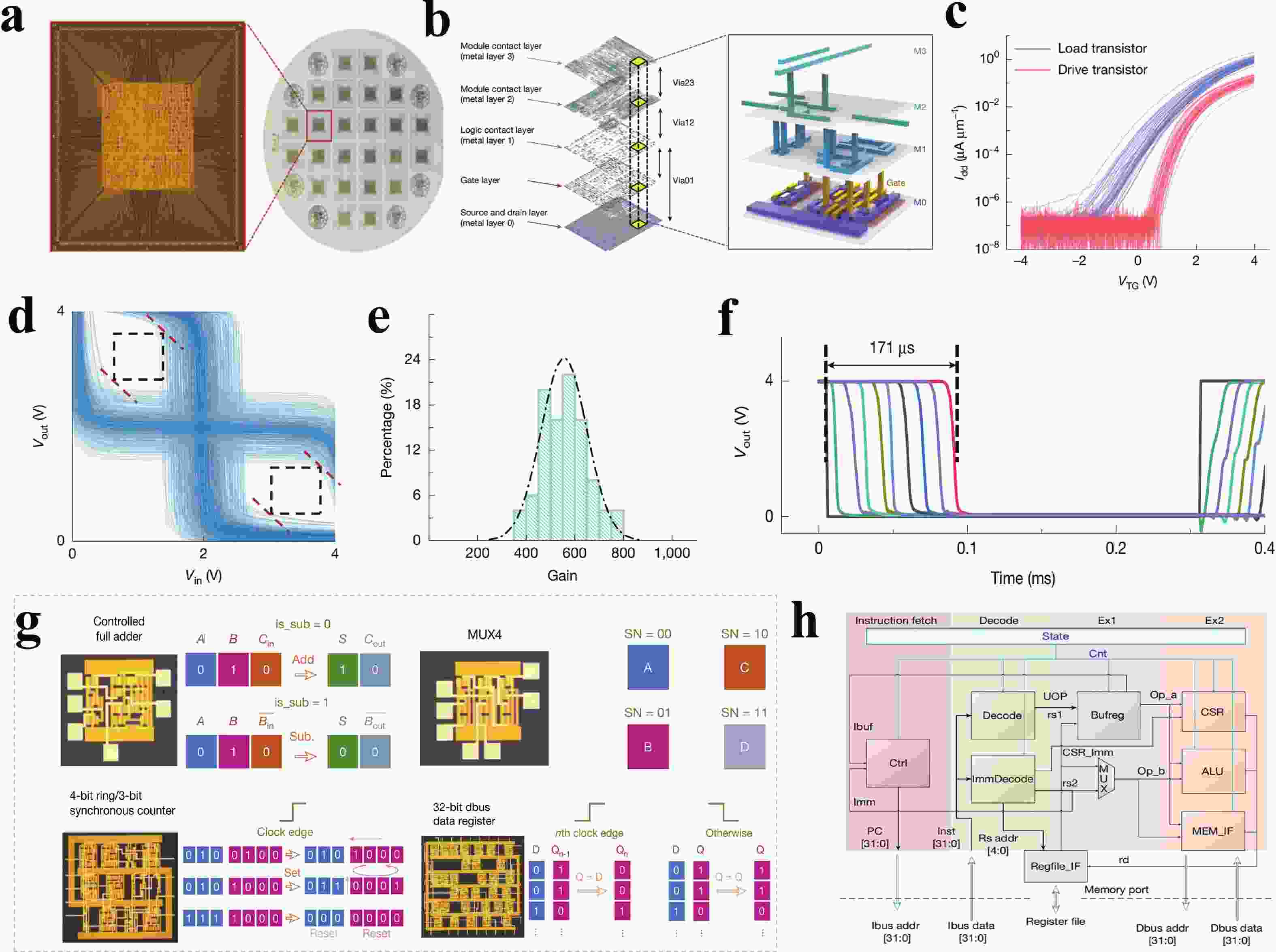
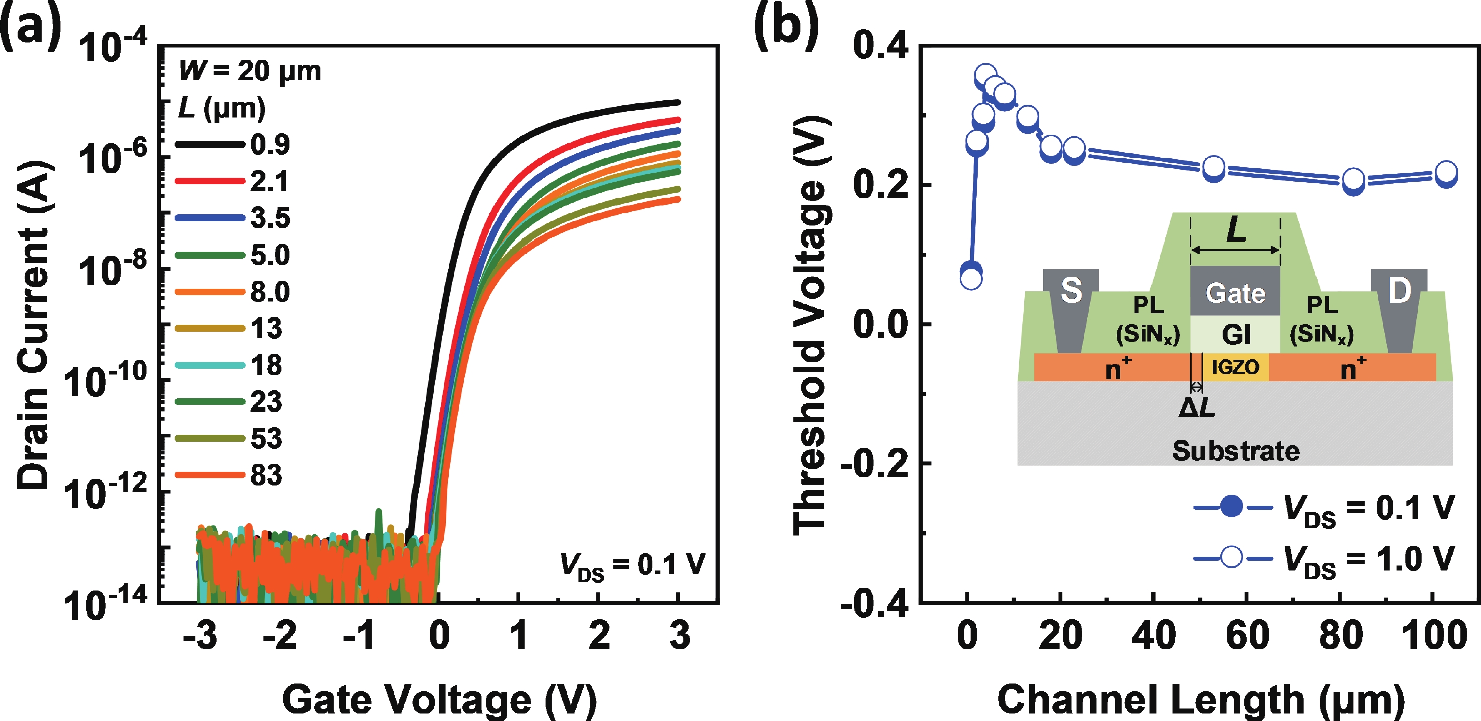
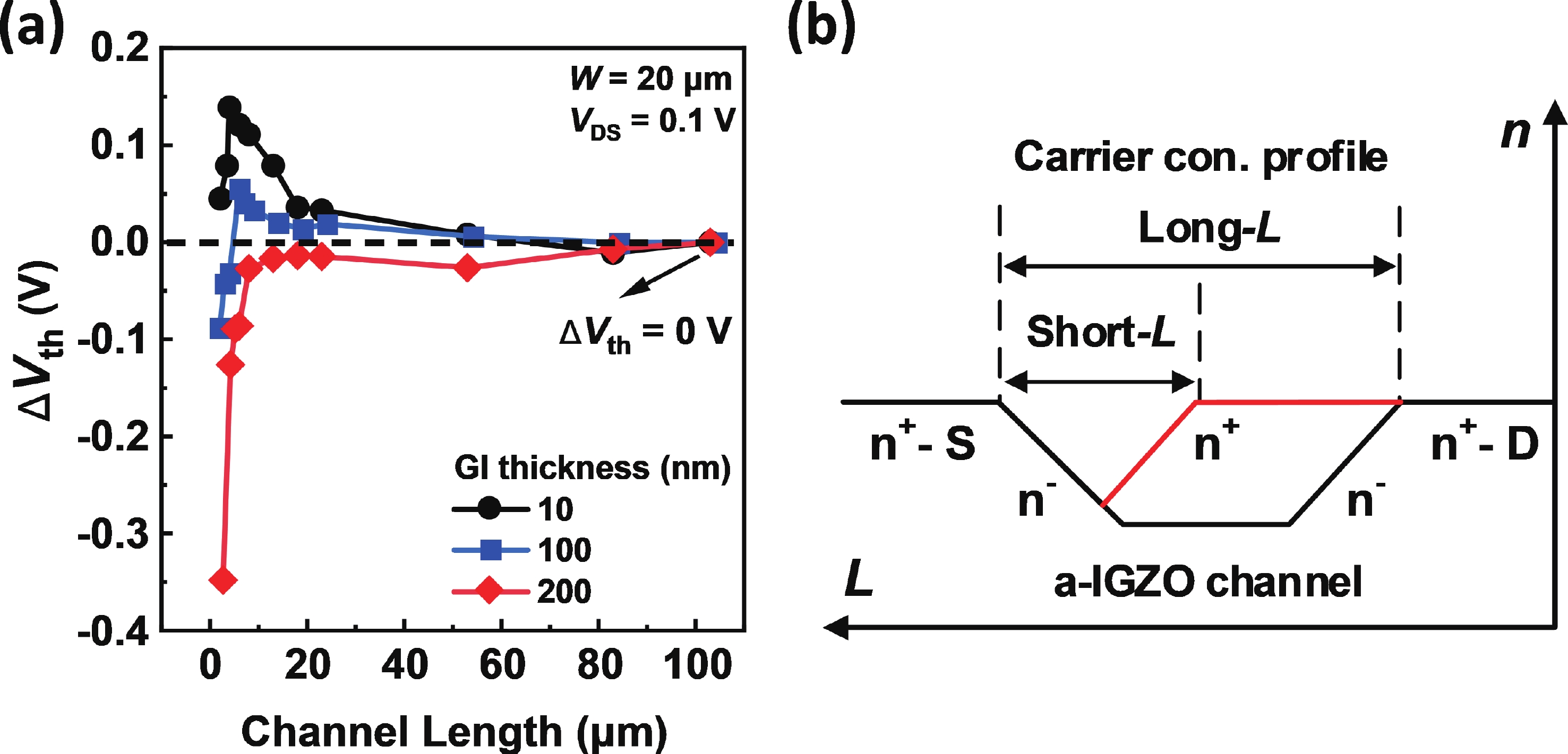
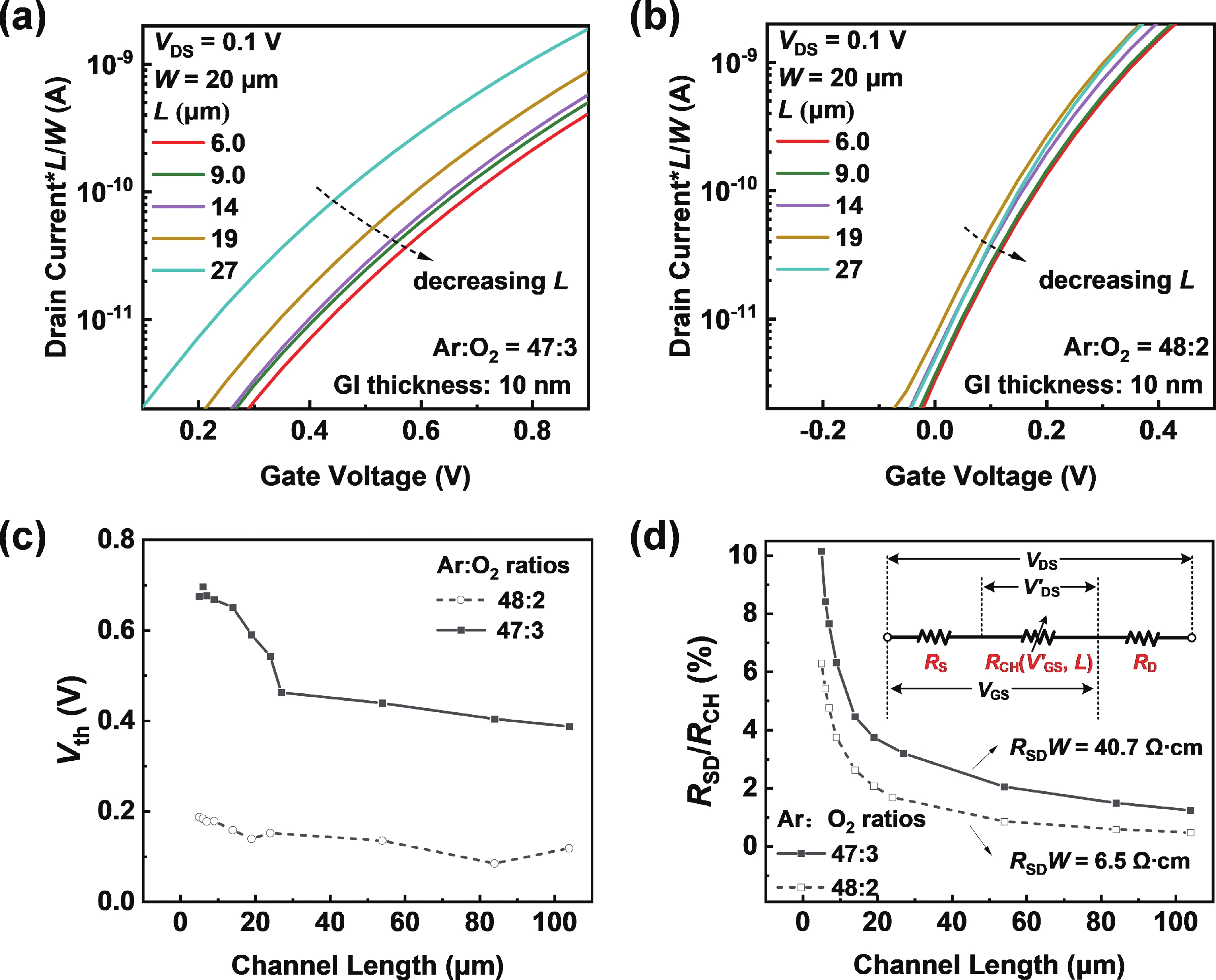
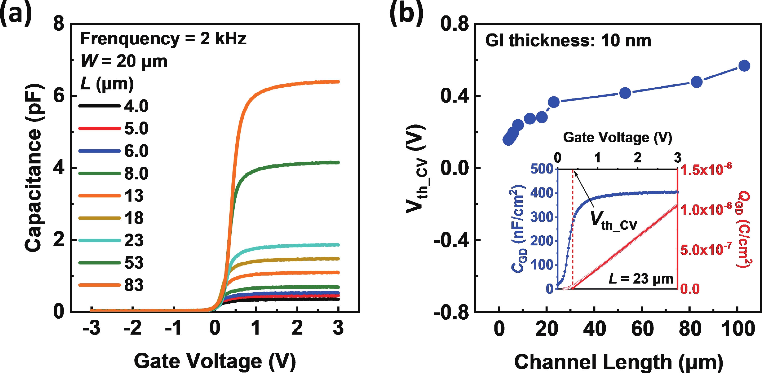
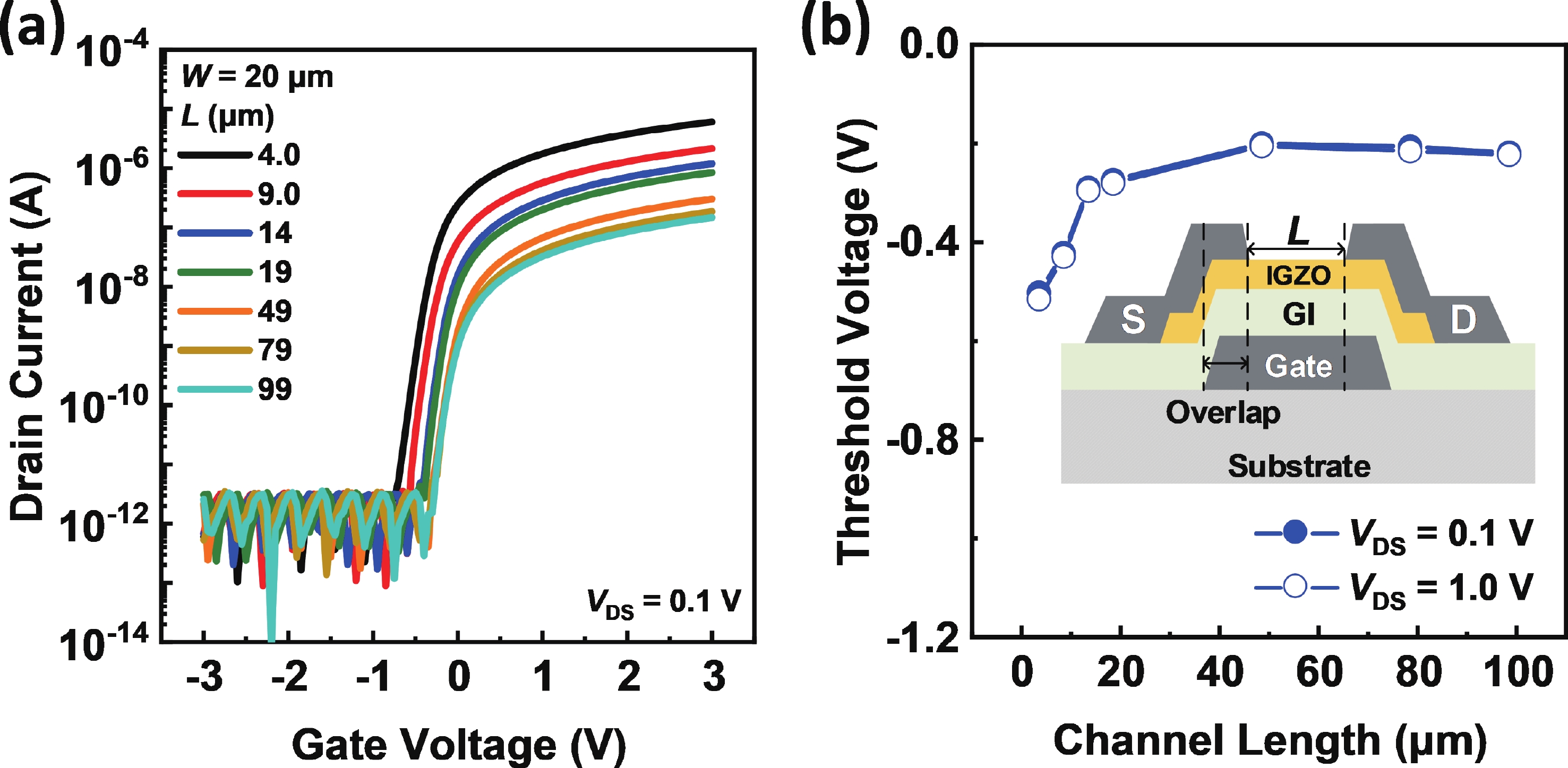
Besides the common short-channel effect (SCE) of threshold voltage (Vth) roll-off during the channel length (L) downscaling of InGaZnO (IGZO) thin-film transistors (TFTs), an opposite Vth roll-up was reported in this work. Both roll-off and roll-up effects of Vth were comparatively investigated on IGZO transistors with varied gate insulator (GI), source/drain (S/D), and device architecture. For IGZO transistors with thinner GI, the SCE was attenuated due to the enhanced gate controllability over the variation of channel carrier concentration, while the Vth roll-up became more noteworthy. The latter was found to depend on the relative ratio of S/D series resistance (RSD) over channel resistance (RCH), as verified on transistors with different S/D. Thus, an ideal S/D engineering with small RSD but weak dopant diffusion is highly expected during the downscaling of L and GI in IGZO transistors.
J. Semicond.
2025, 46(8): 082302 doi: 10.1088/1674-4926/24120027
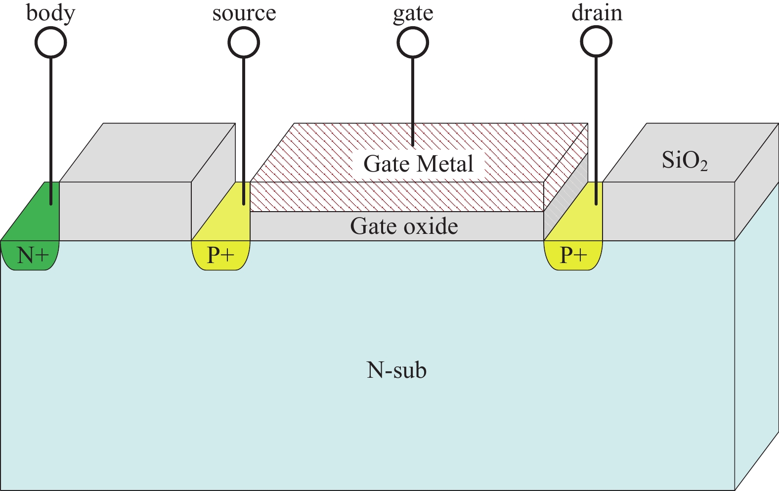
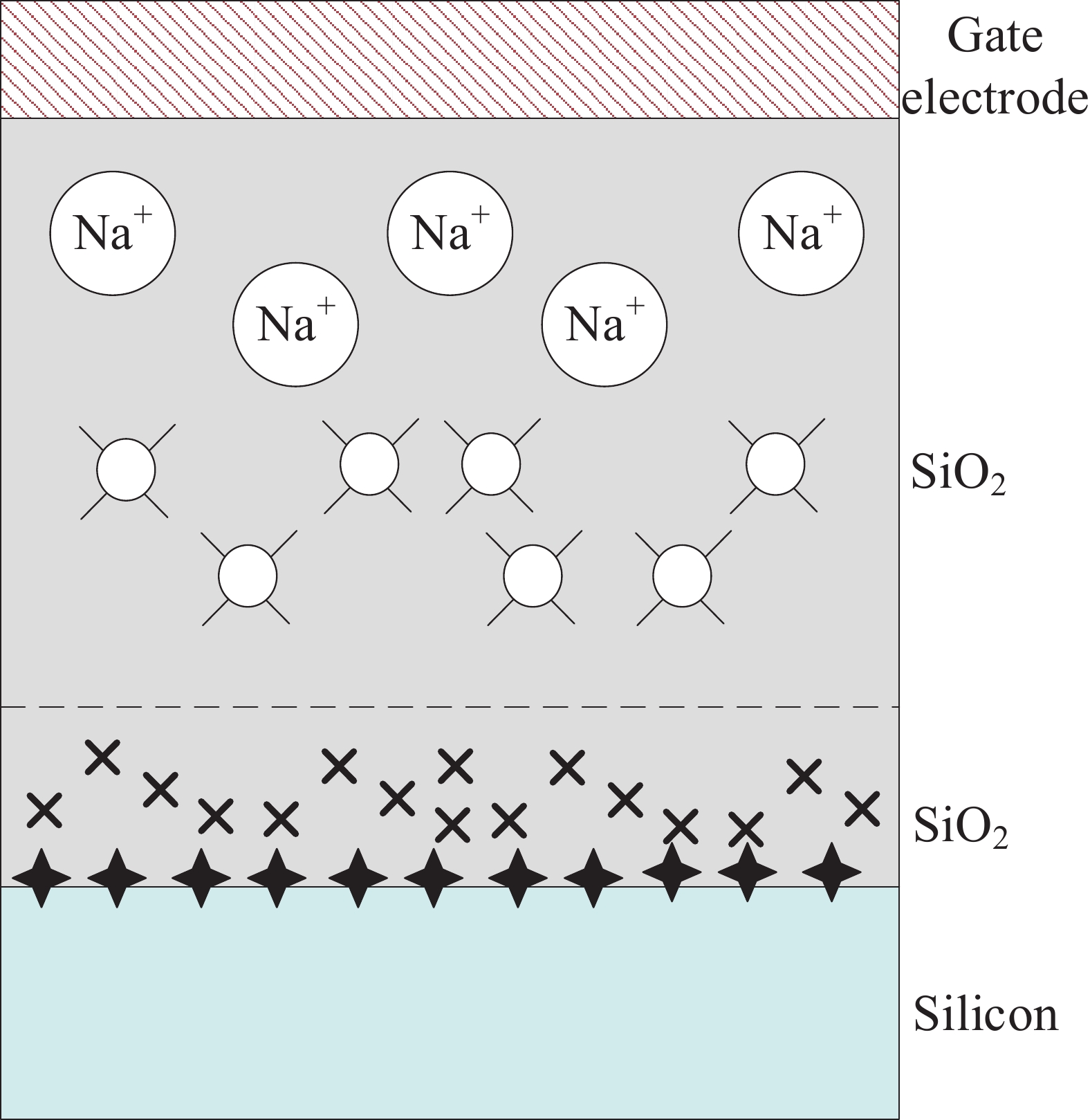
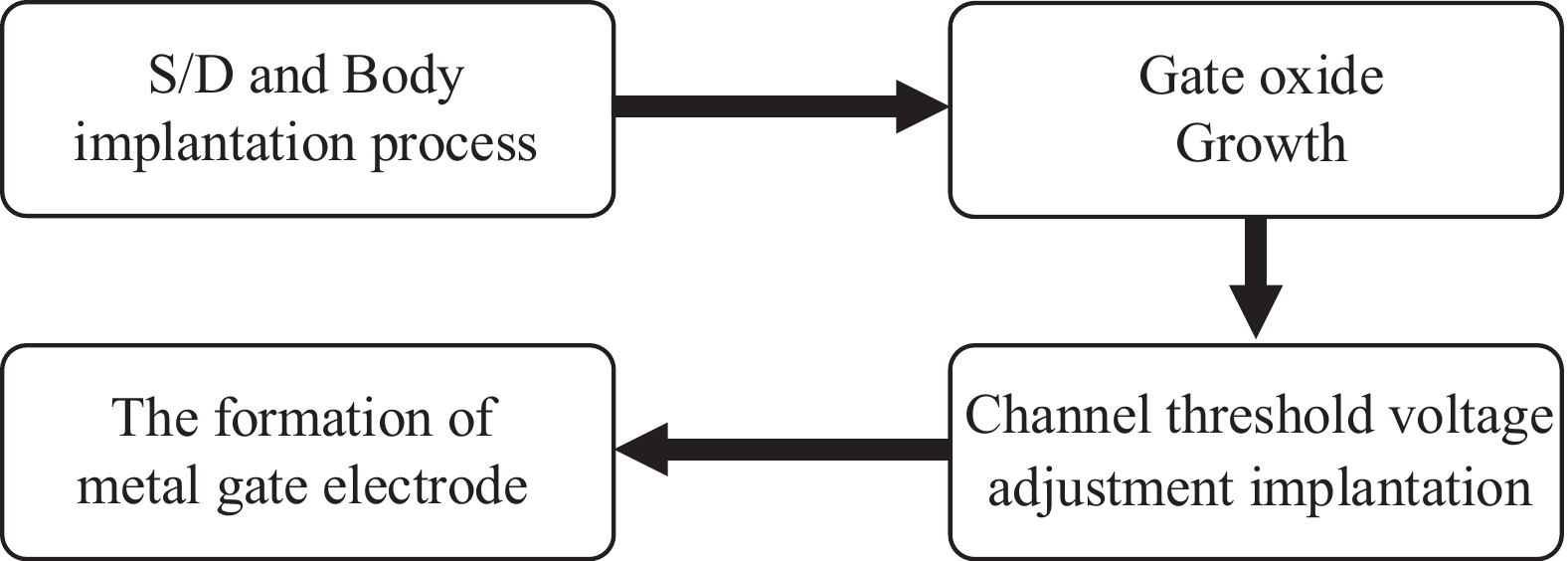
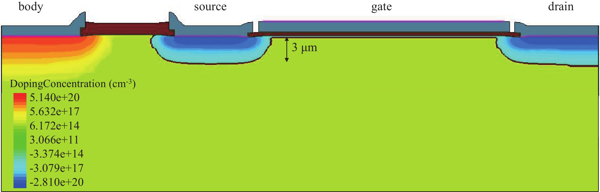
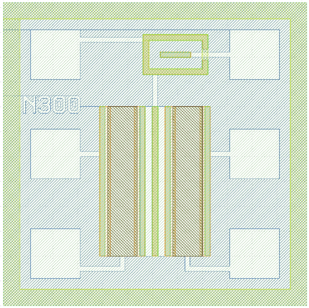
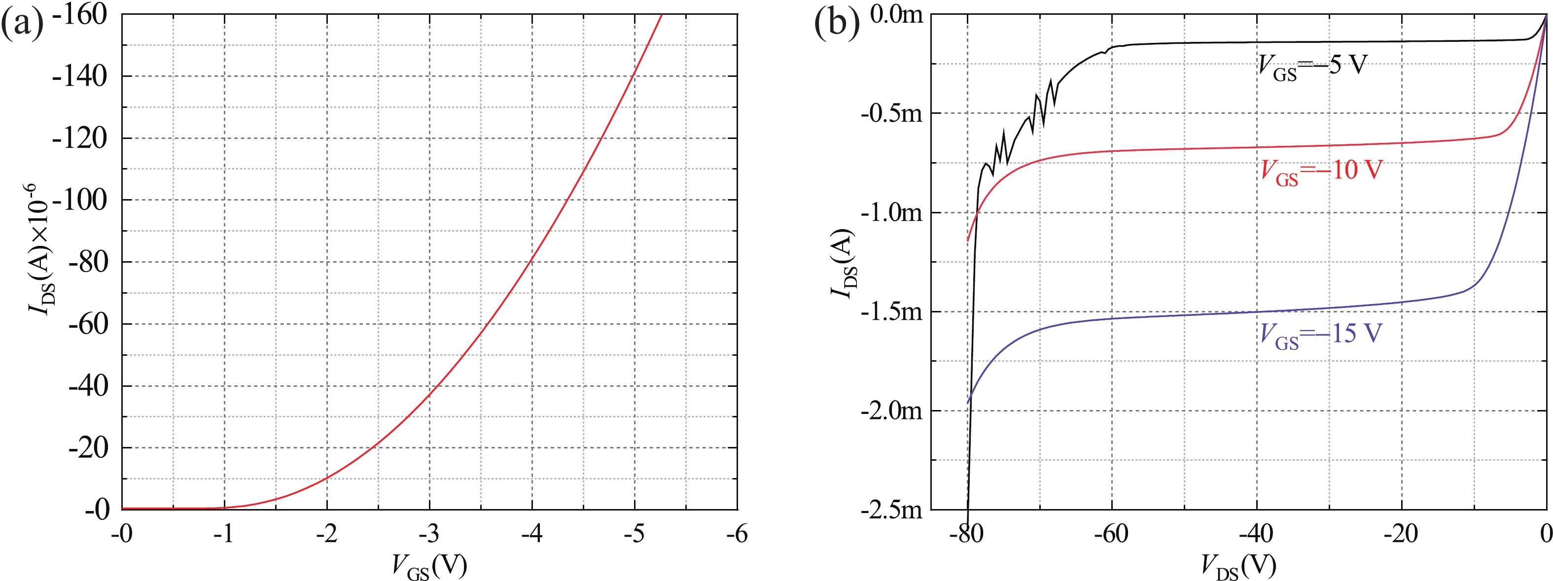
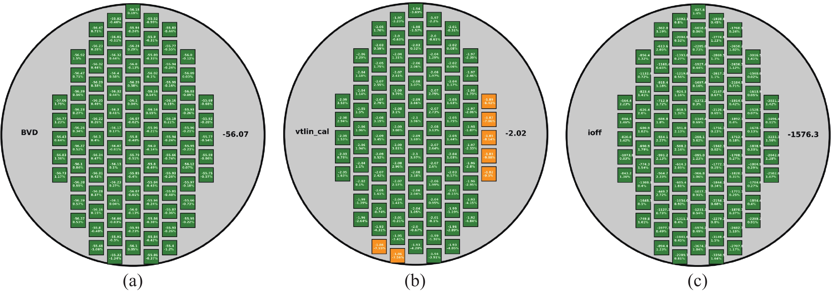
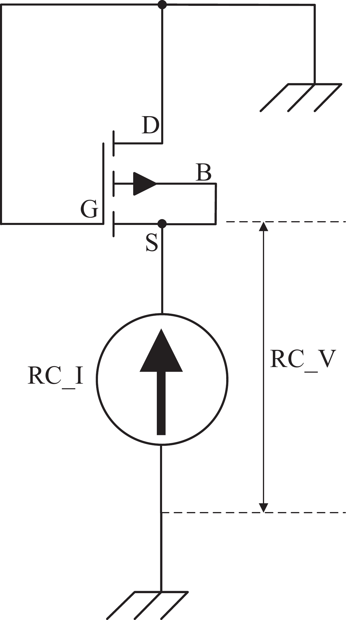
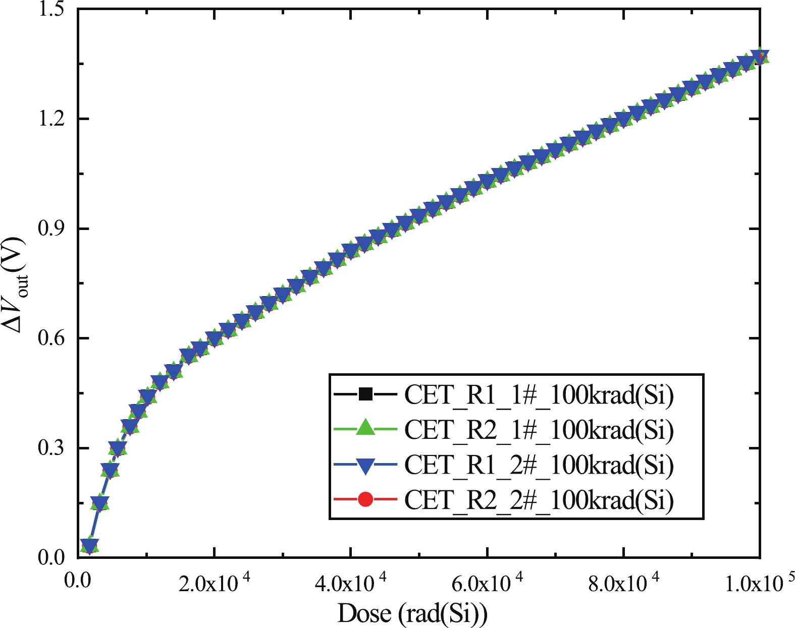
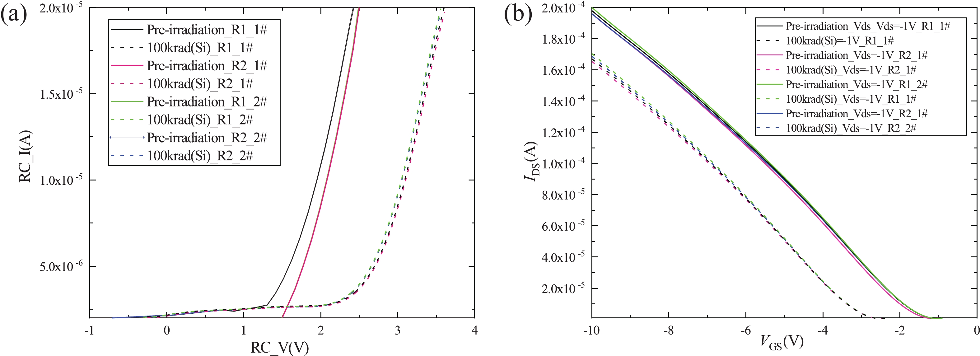
The radiation-sensitive field effect transistors (RADFET) radiation dosimeter is a type of radiation detector based on the total dose effects of the p-channel metal−oxide−semiconductor (PMOS) transistor. The RADFET chip was fabricated in United Microelectronics Center 8-inch process with a six-layer photomask. The chip including two identical PMOS transistors, occupies a size of 610 µm × 610 µm. Each PMOS has a W/L ratio of 300 µm/50 µm, and a 400 nm thick gate oxide, which is formed by a dry-wet-dry oxygen process. The wet oxygen-formed gate oxide with more traps can capture more holes during irradiation, thus significantly changing the PMOS threshold voltage. Pre-irradiation measurement results from ten test chips show that the initial average voltage of the PMOS is 1.961 V with a dispersion of 5.7%. The irradiation experiment is conducted in a cobalt source facility with a dose rate of 50 rad(Si)/s. During irradiation, a constant current source circuit of 10 µA was connected to monitoring the shift in threshold voltage under different total dose. When the total dose is 100 krad(Si), the shift in threshold voltage was approximately 1.37 V, which demonstrates that an excellent radiation function was achieved.
J. Semicond.
2025, 46(8): 082501 doi: 10.1088/1674-4926/25010005
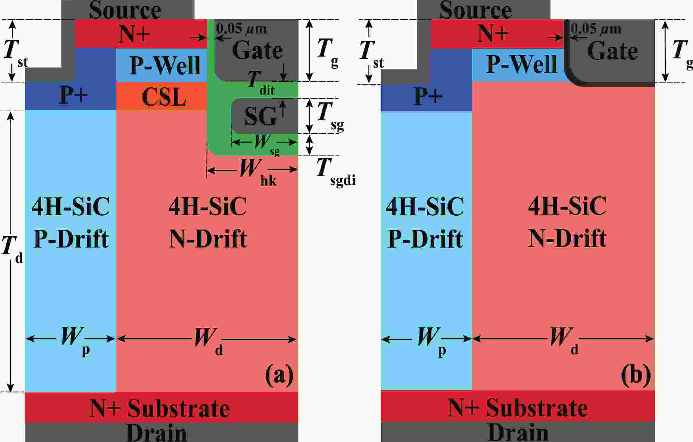
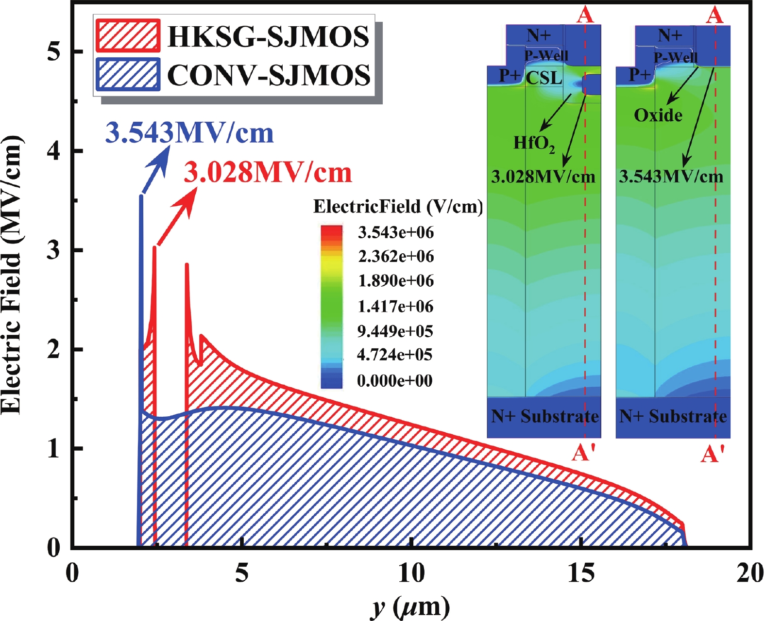
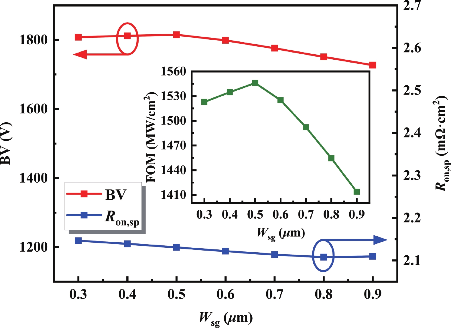
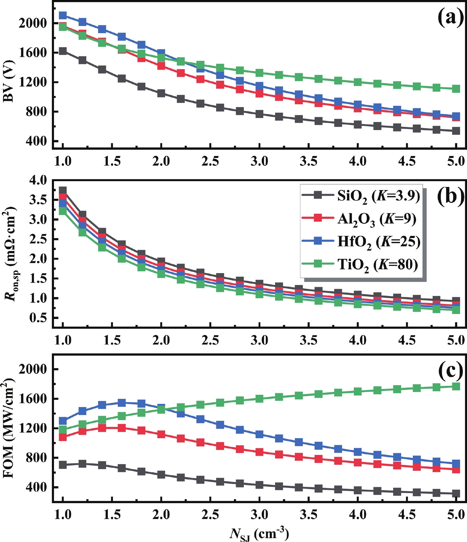
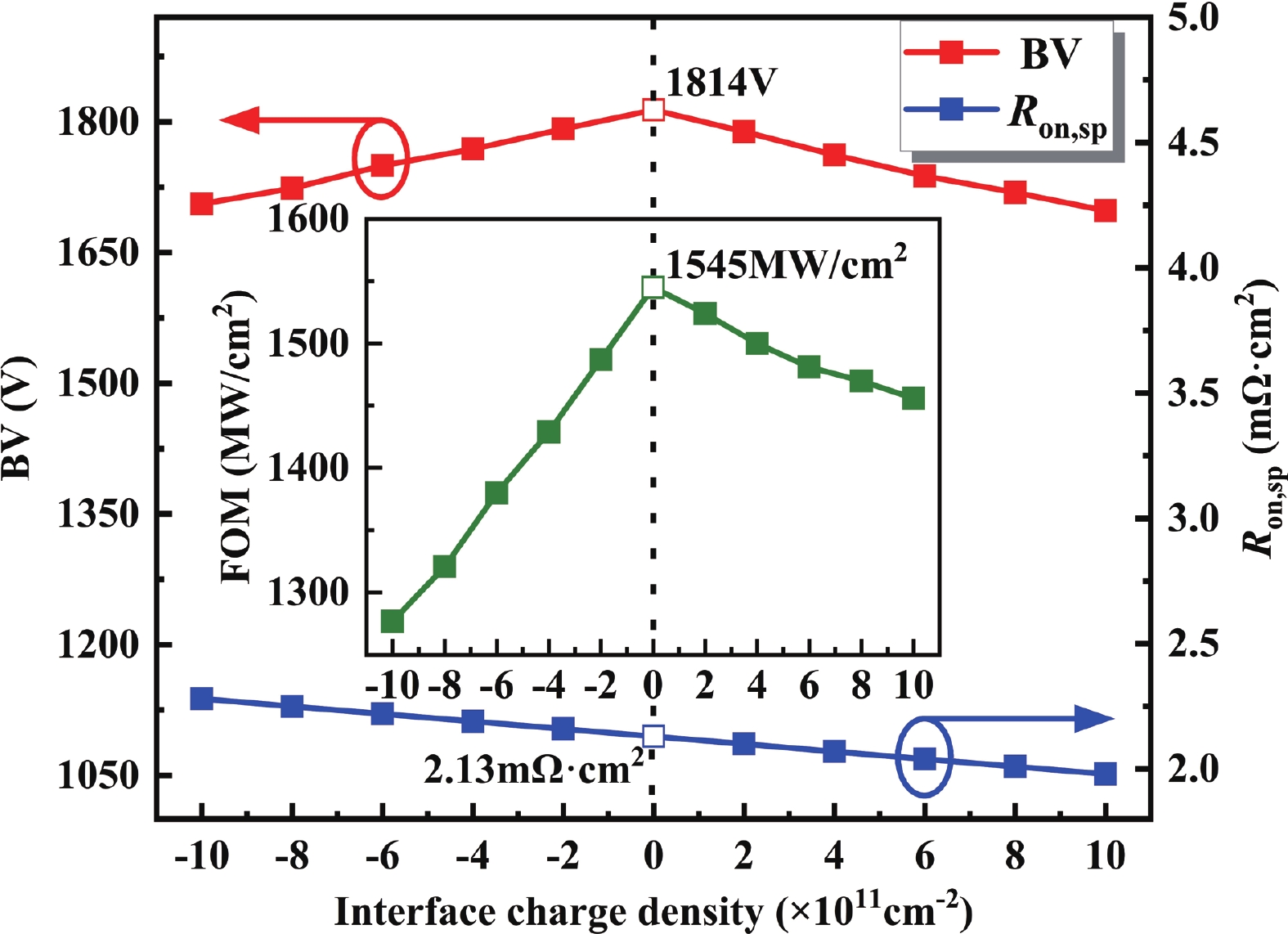
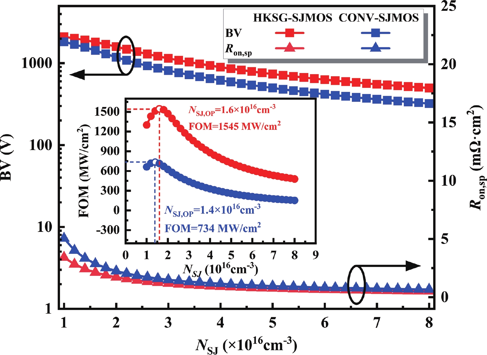
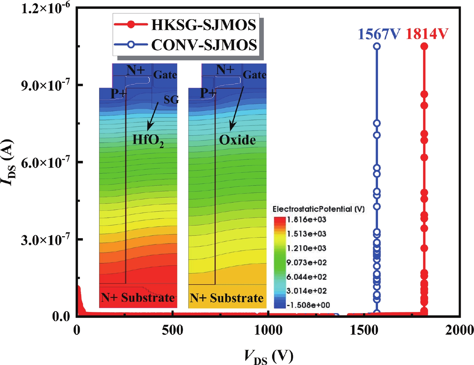
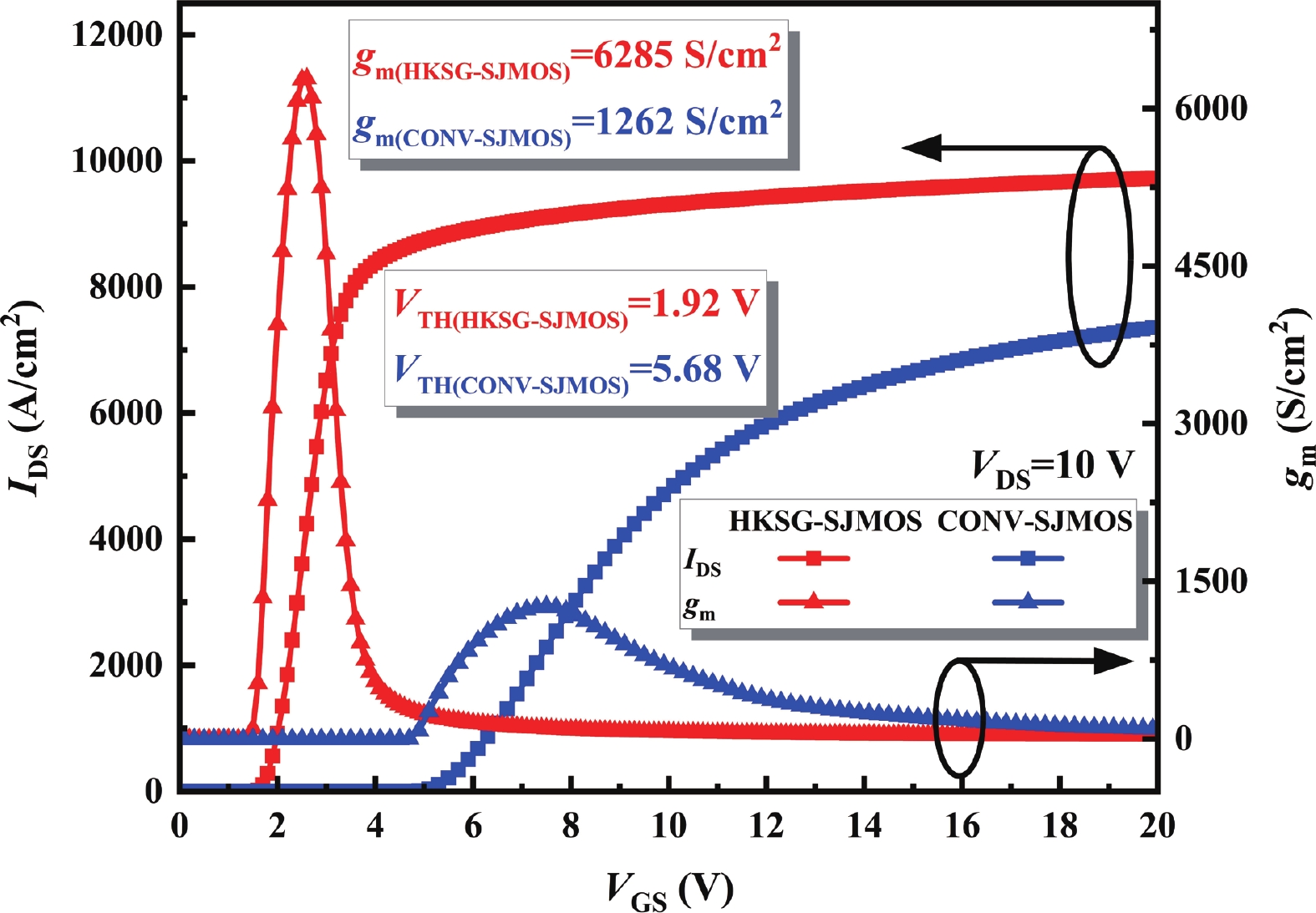
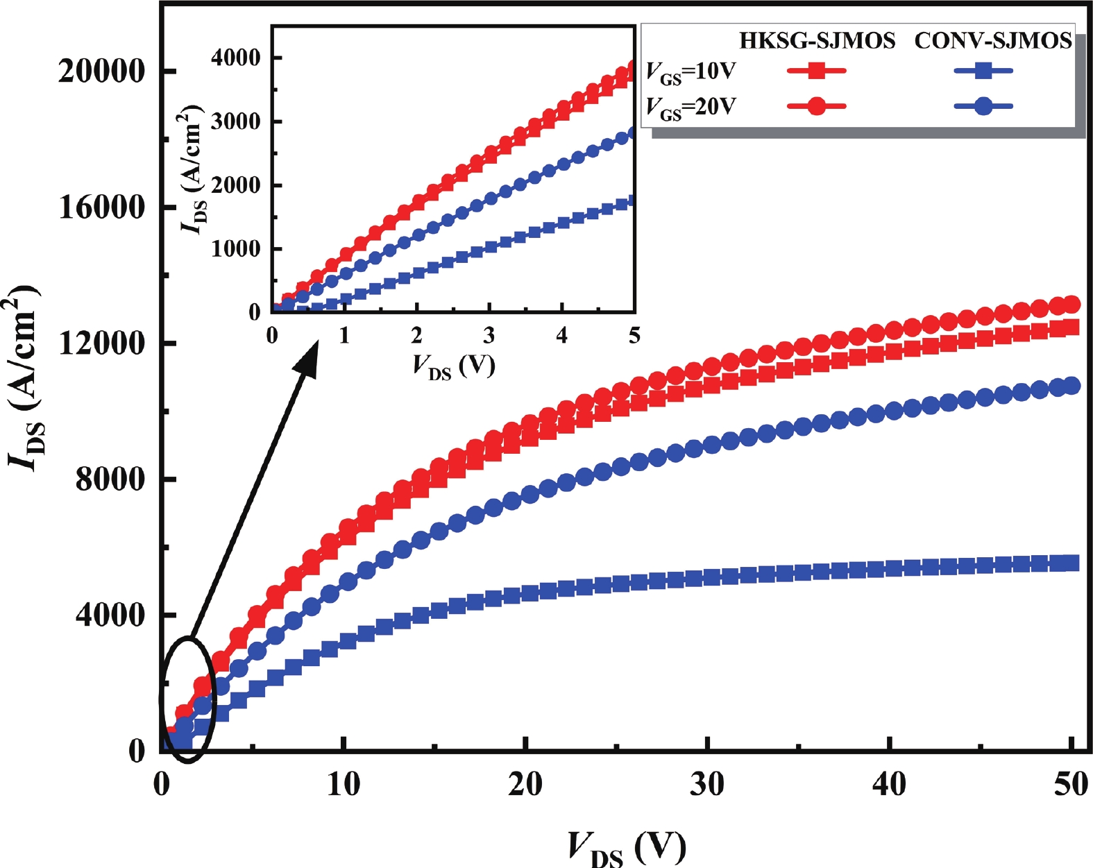
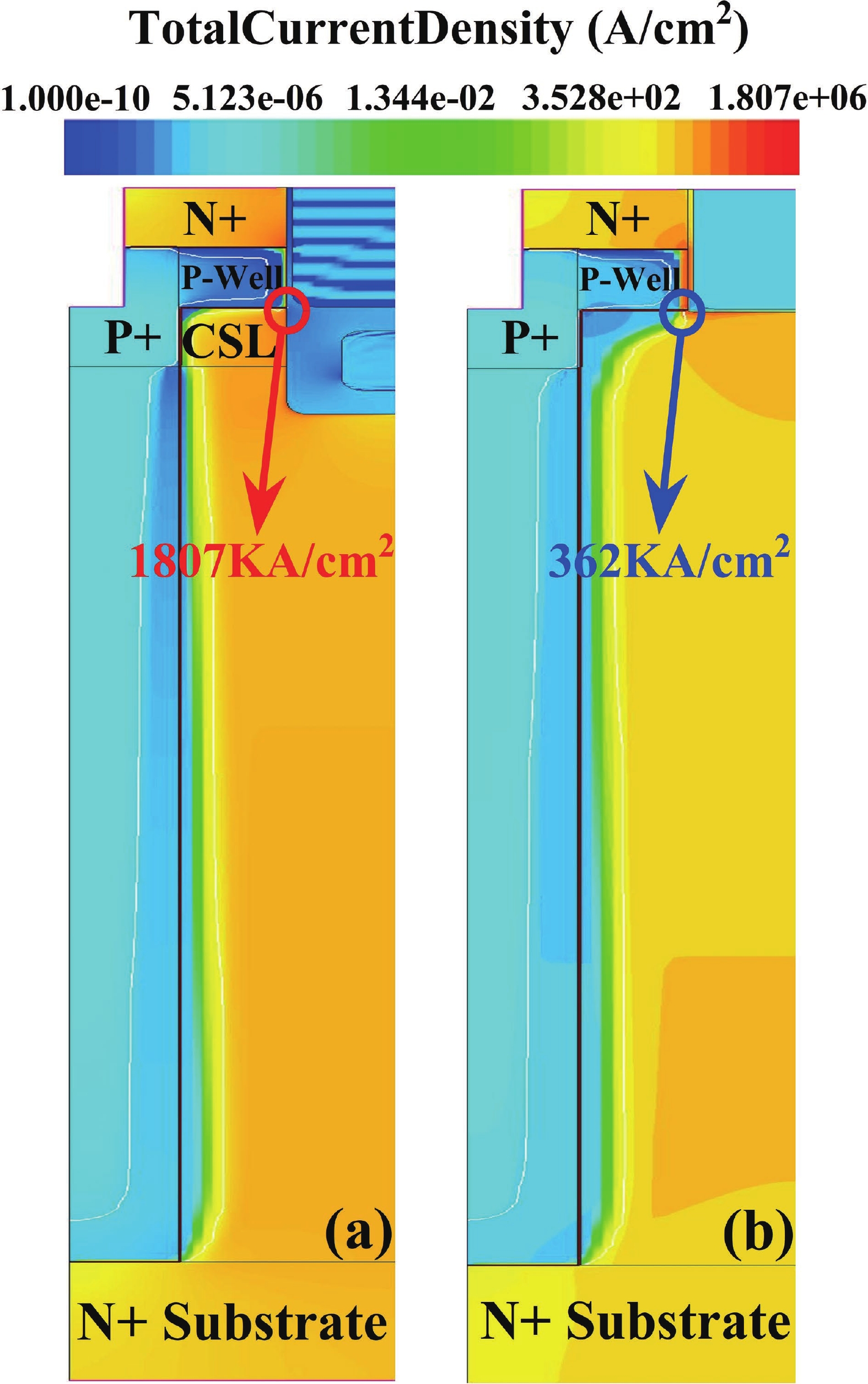
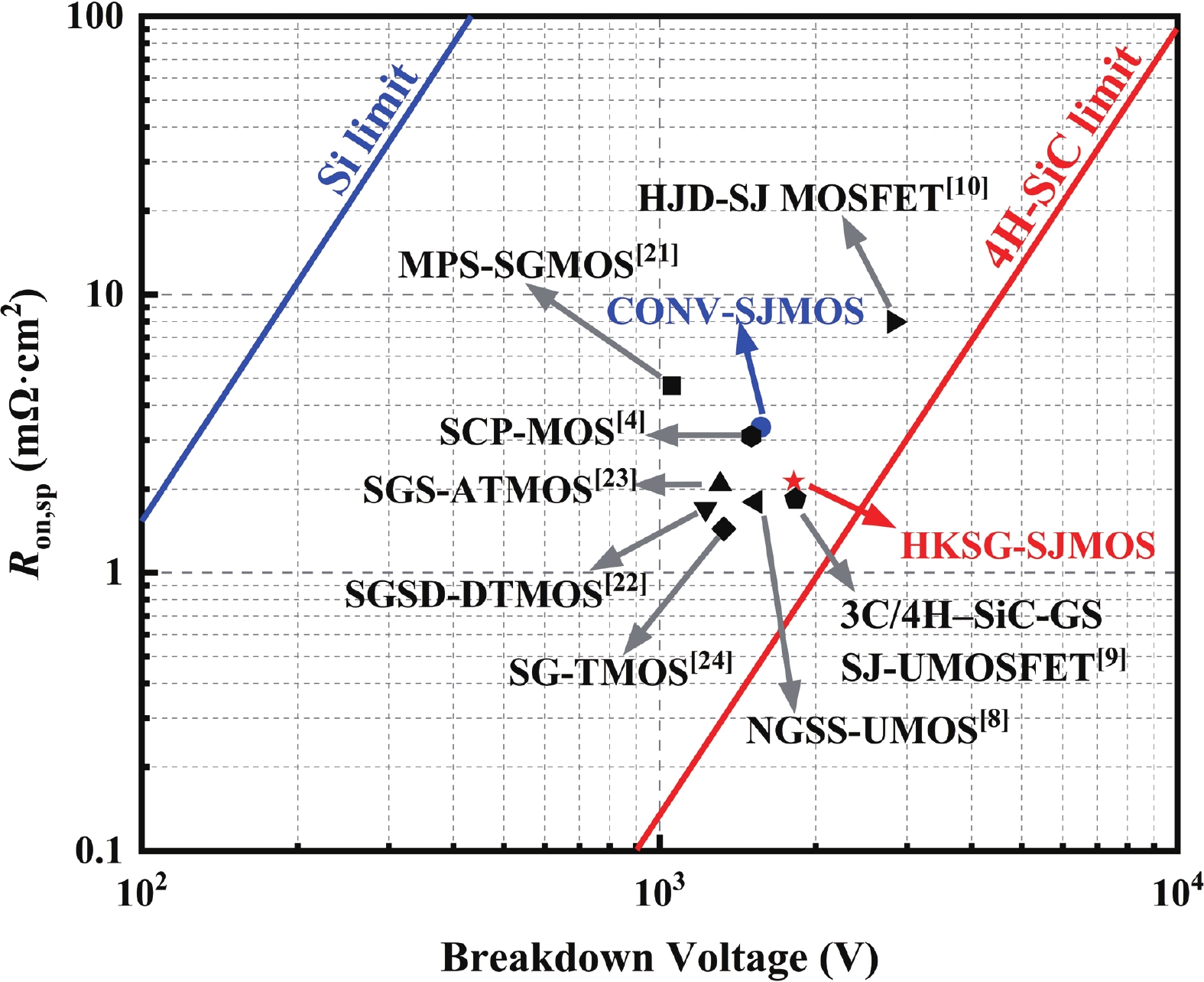
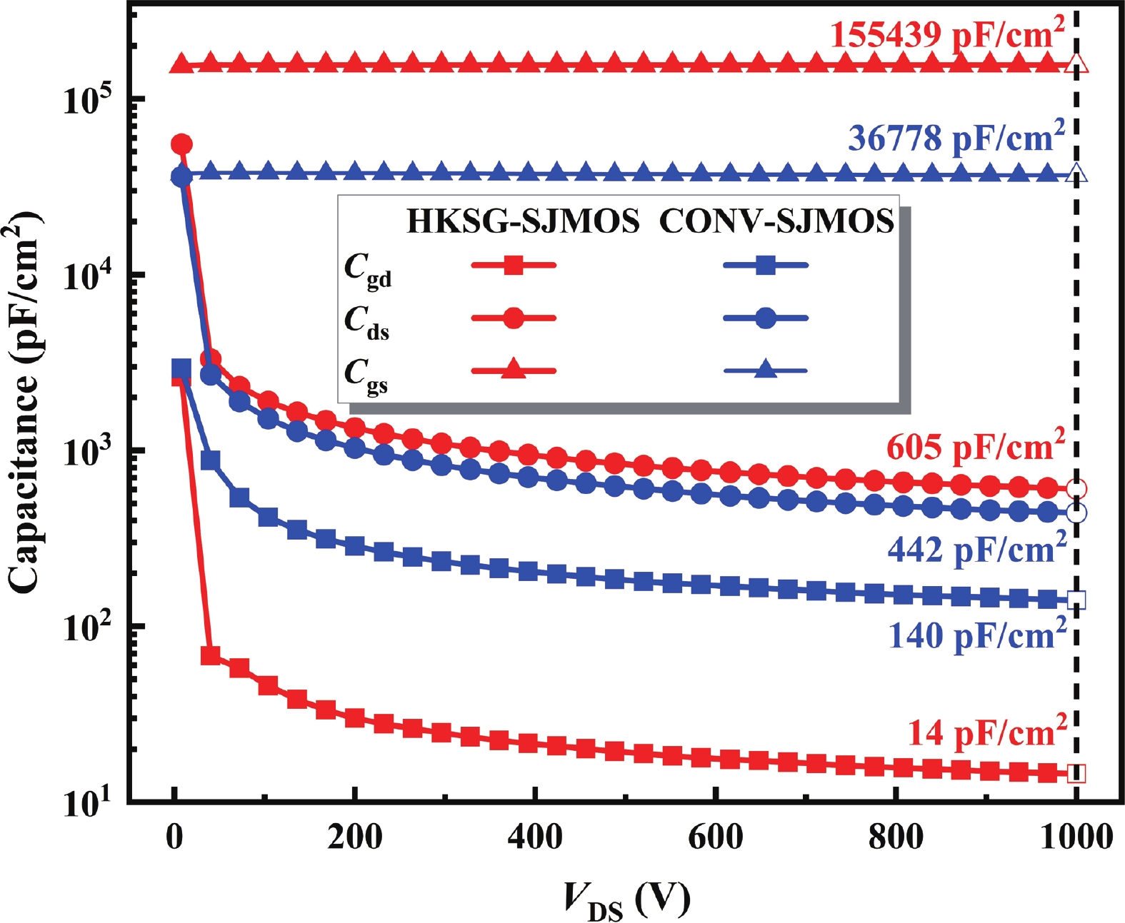
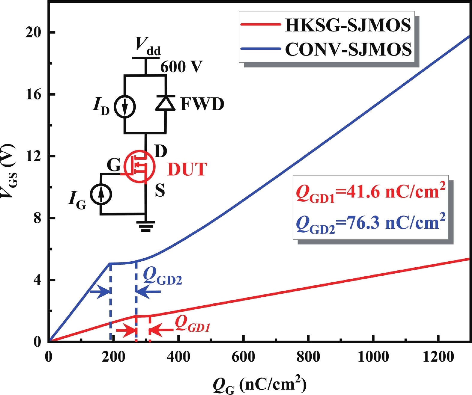
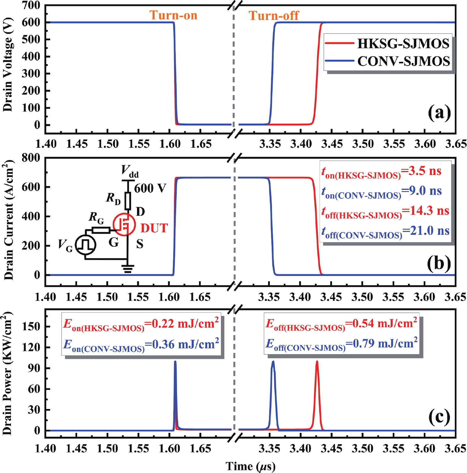
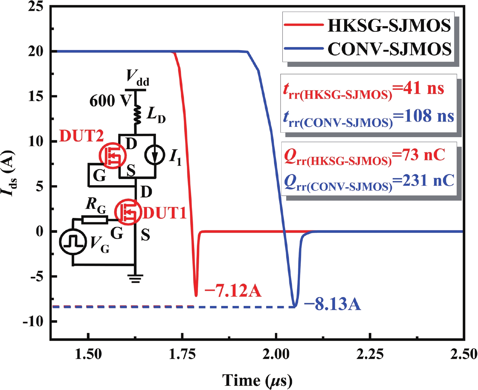
A 4H-SiC superjunction (SJ) MOSFET (SJMOS) with integrated high-K gate dielectric and split gate (HKSG-SJMOS) is proposed in this paper. The key features of HKSG-SJMOS involve the utilization of high-K (HK) dielectric as the gate dielectric, which surrounds the source-connected split gate (SG) and metal gate. The high-K gate dielectric optimizes the electric field distribution within the drift region, creating a low-resistance conductive channel. This enhancement leads to an increase in the breakdown voltage (BV) and a reduction in the specific on resistance (Ron,sp). The introduction of split gate surrounded by high-K dielectric reduces the gate−drain capacitance (Cgd) and gate−drain charge (Qgd), which improves the switching characteristics. The simulation results indicate that compared to conventional 4H-SiC SJMOS, the HKSG-SJMOS exhibits a 110.5% enhancement in figure of merit (FOM, FOM = BV2/Ron,sp), a 93.6% reduction in the high frequency figure of merit (HFFOM) of Ron,sp·Cgd, and reductions in turn-on loss (Eon) and turn-off loss (Eoff) by 38.3% and 31.6%, respectively. Furthermore, the reverse recovery characteristics of HKSG-SJMOS has also discussed, revealing superior performance compared to conventional 4H-SiC SJMOS.
J. Semicond.
2025, 46(8): 082502 doi: 10.1088/1674-4926/25020018
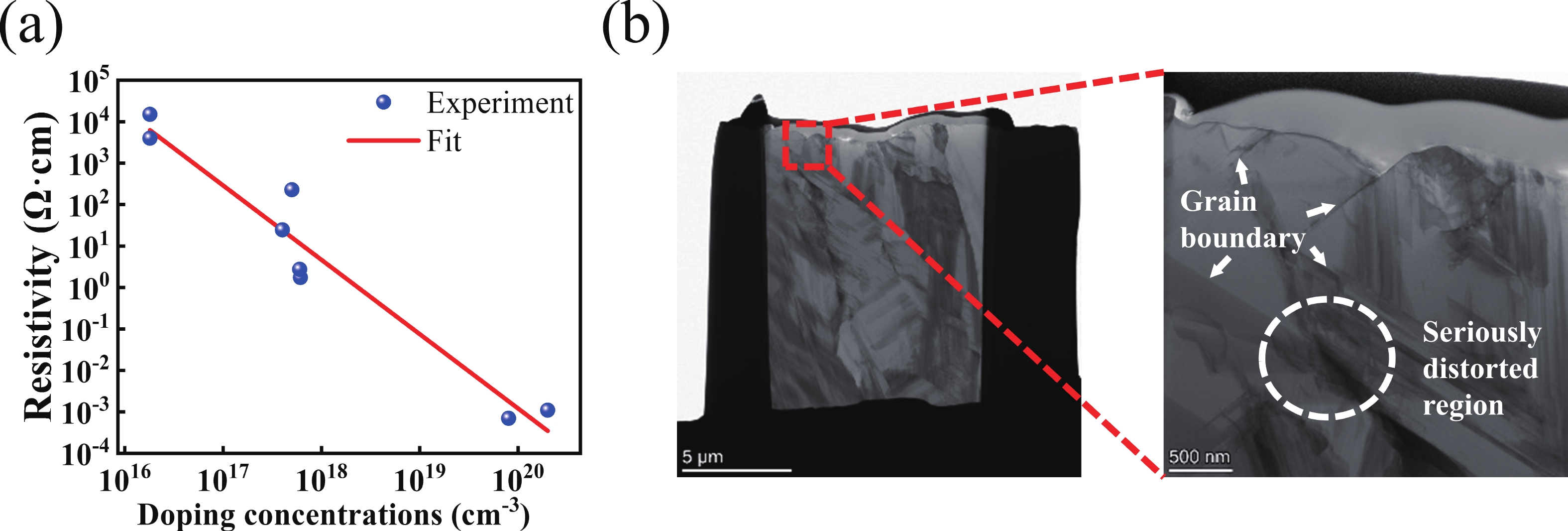
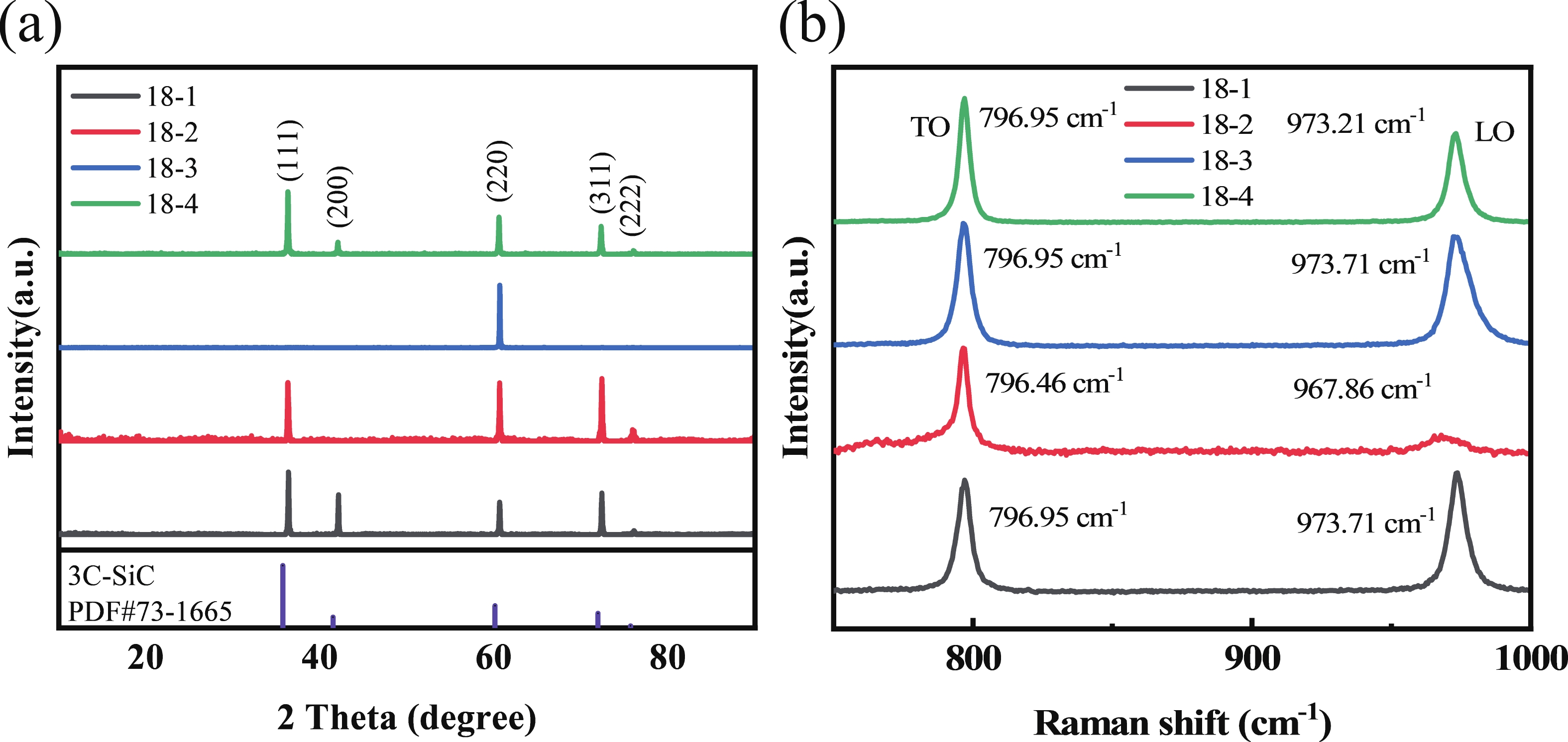
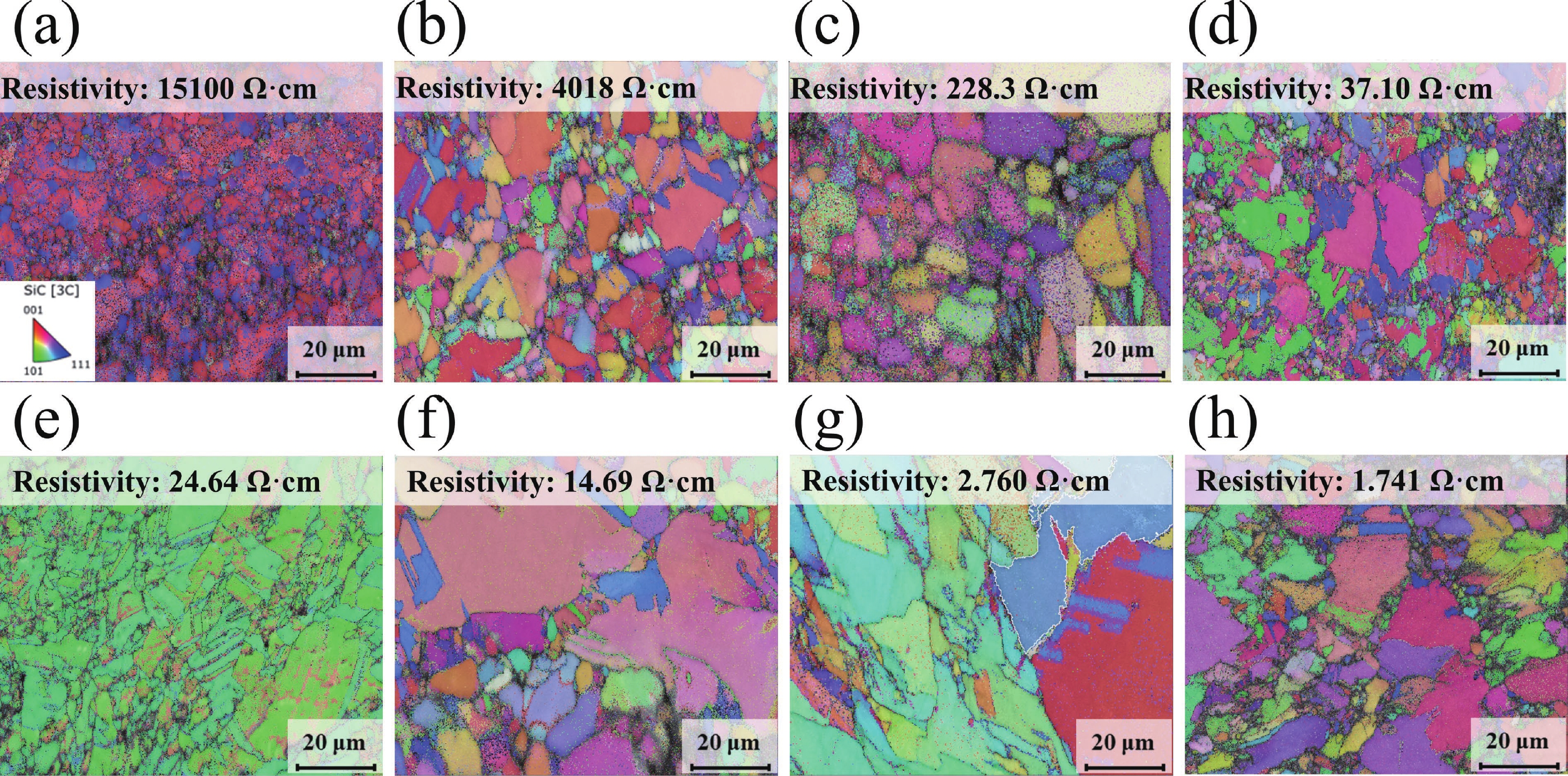
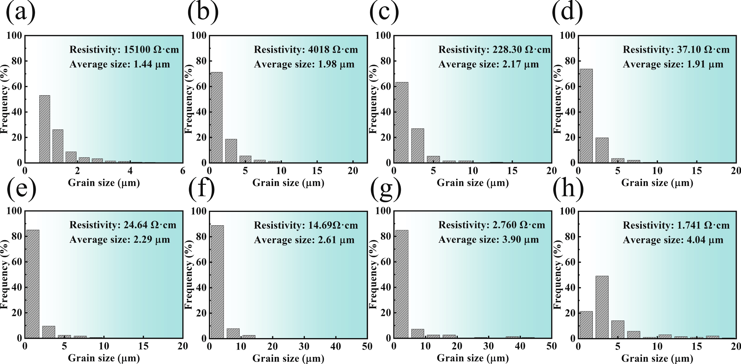
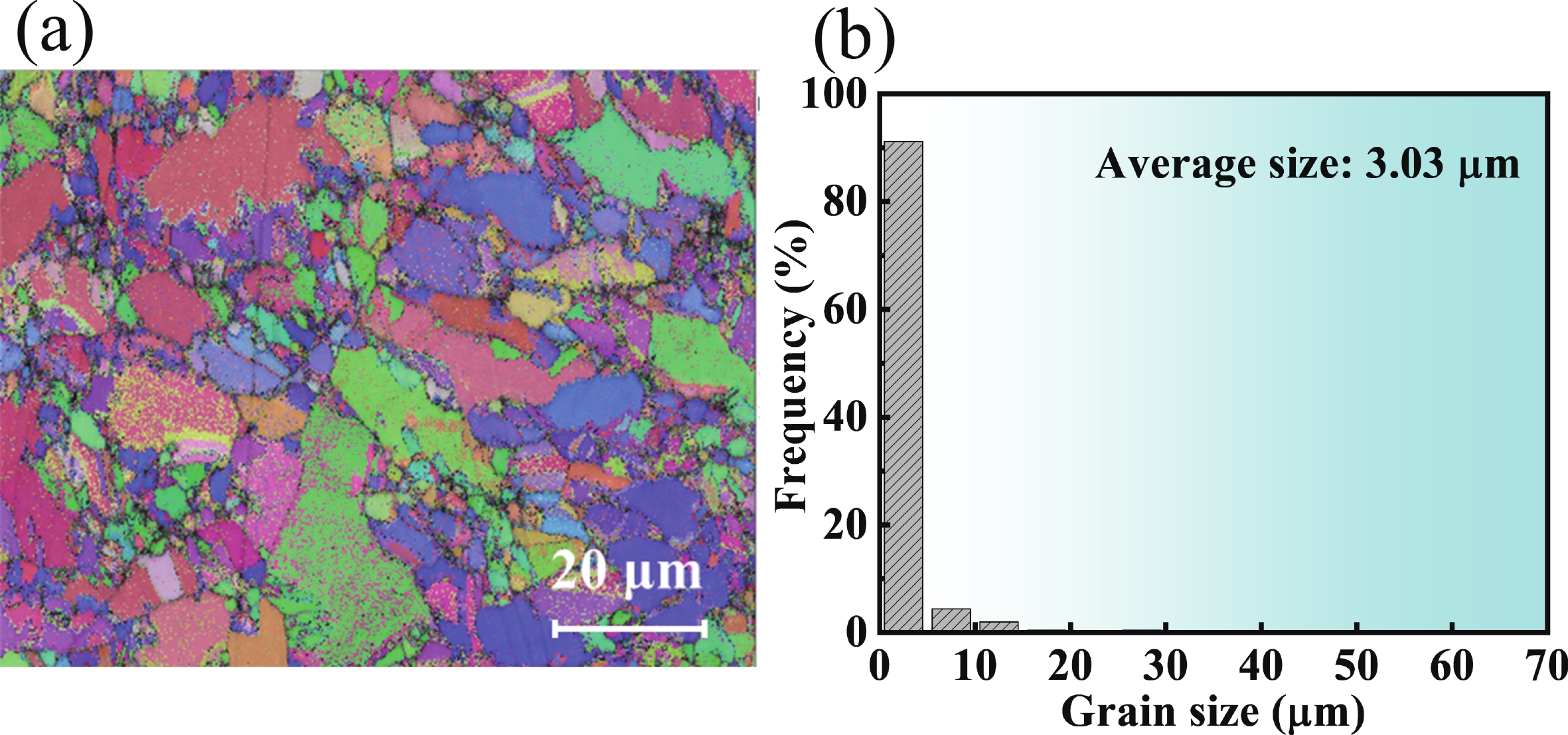
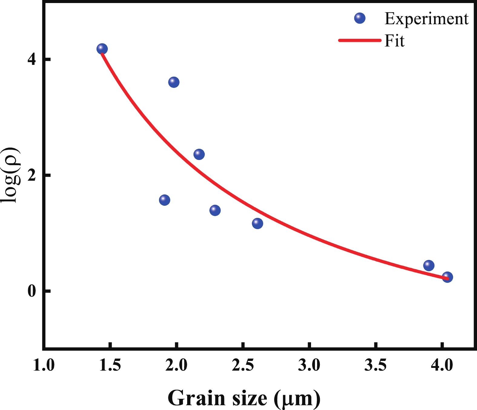
Silicon carbide offers distinct advantages in the field of power electronic devices. However, manufacturing processes remain a significant barrier to its widespread adoption. Polycrystalline SiC is less expensive and easier to produce than single crystal. But stabilizing and controlling its performance are critical challenges that must be addressed urgently. Due to its material properties and excellent performance in applications, 3C-SiC is gaining increasing attention in research. This article presents the electrical and material properties of a series of polycrystalline 3C-SiC samples and investigates their interrelationship. The samples were examined using TEM, which confirmed their polycrystalline structure. Combined with XRD and Raman spectroscopy, the grain orientations within the samples were analyzed, and the presence of stress was verified. EBSD was employed to statistically examine the grain structure and size across samples. For samples with similar doping levels, grain size is the most influential factor in determining electrical characteristics. Further EBSD measurements reveal the relationship between resistivity and grain size as log(ρ) = −1.93 + 8.67/d. These findings provide a foundation for the quantitative control and application of polycrystalline 3C-SiC. This work offers theoretical evidence for optimizing the performance tuning of 3C-SiC ceramics and enhancing their effectiveness in electronic applications.
J. Semicond.
2025, 46(8): 082503 doi: 10.1088/1674-4926/25020008
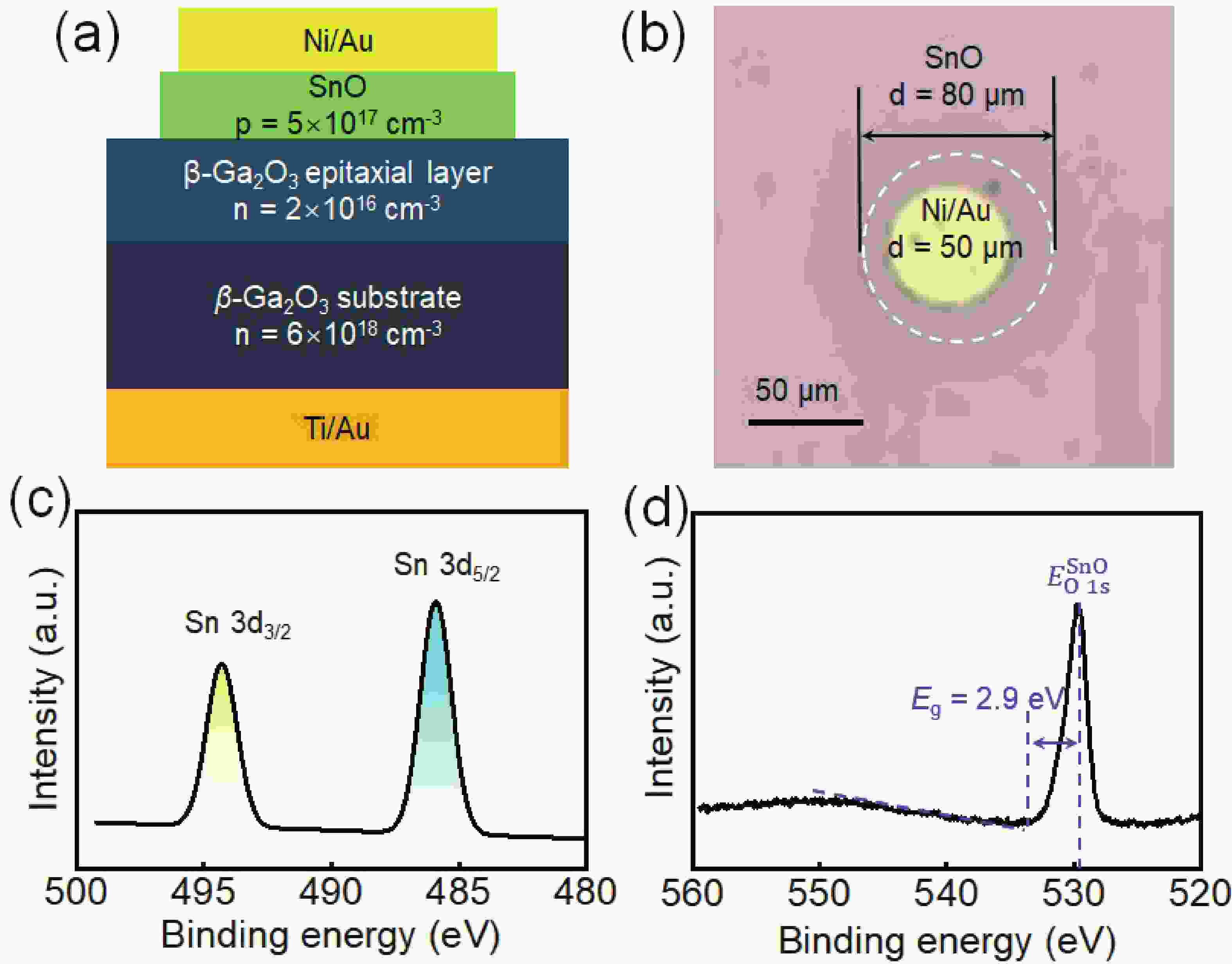
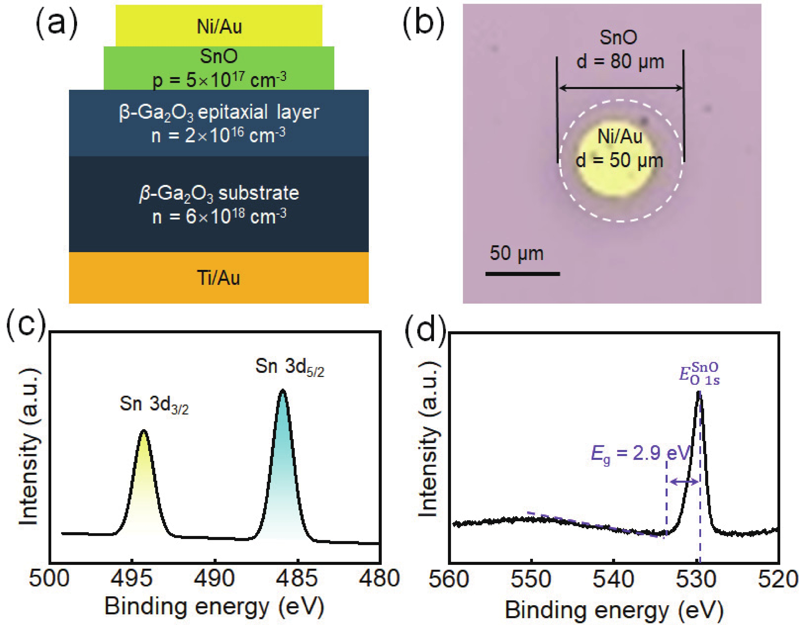
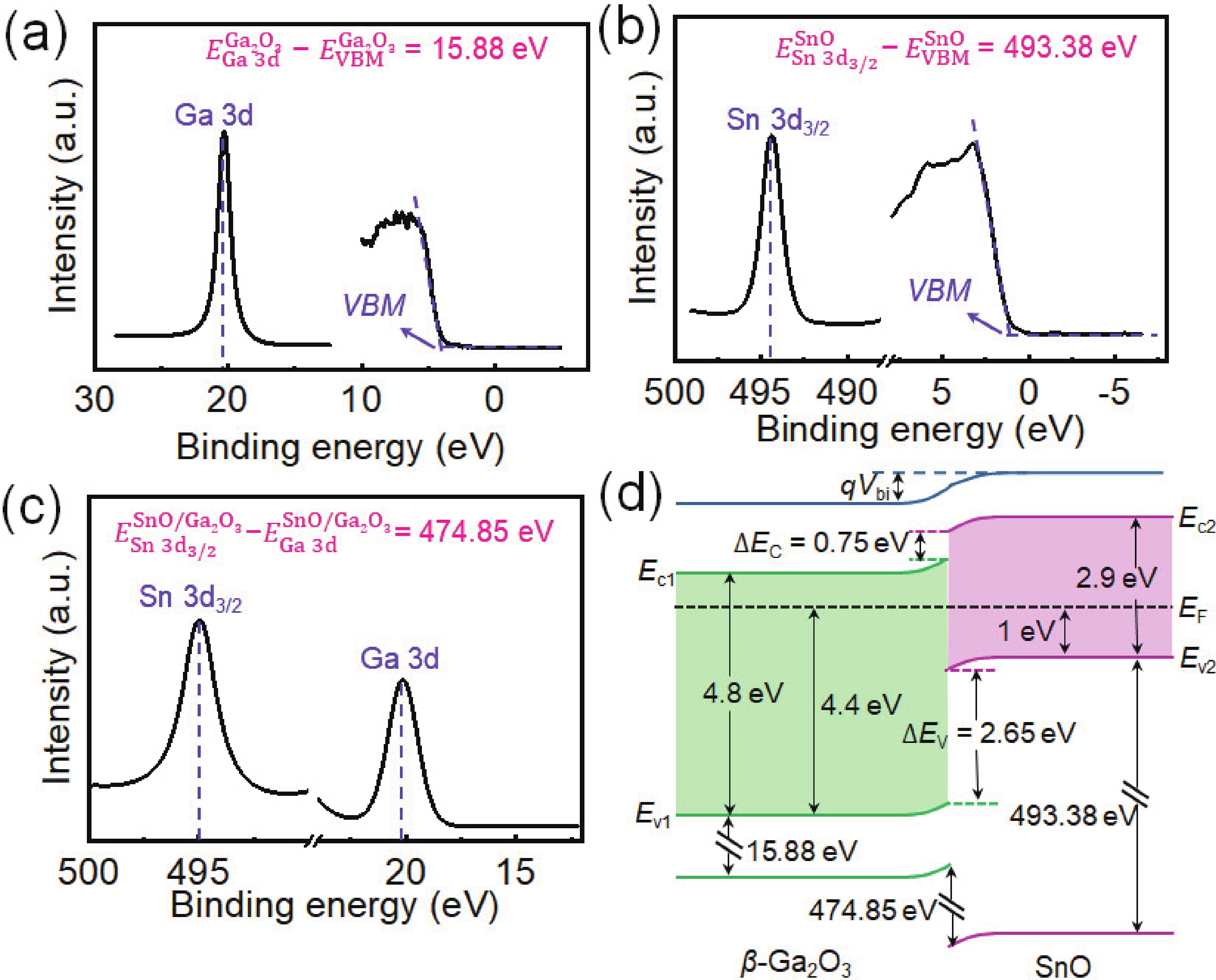
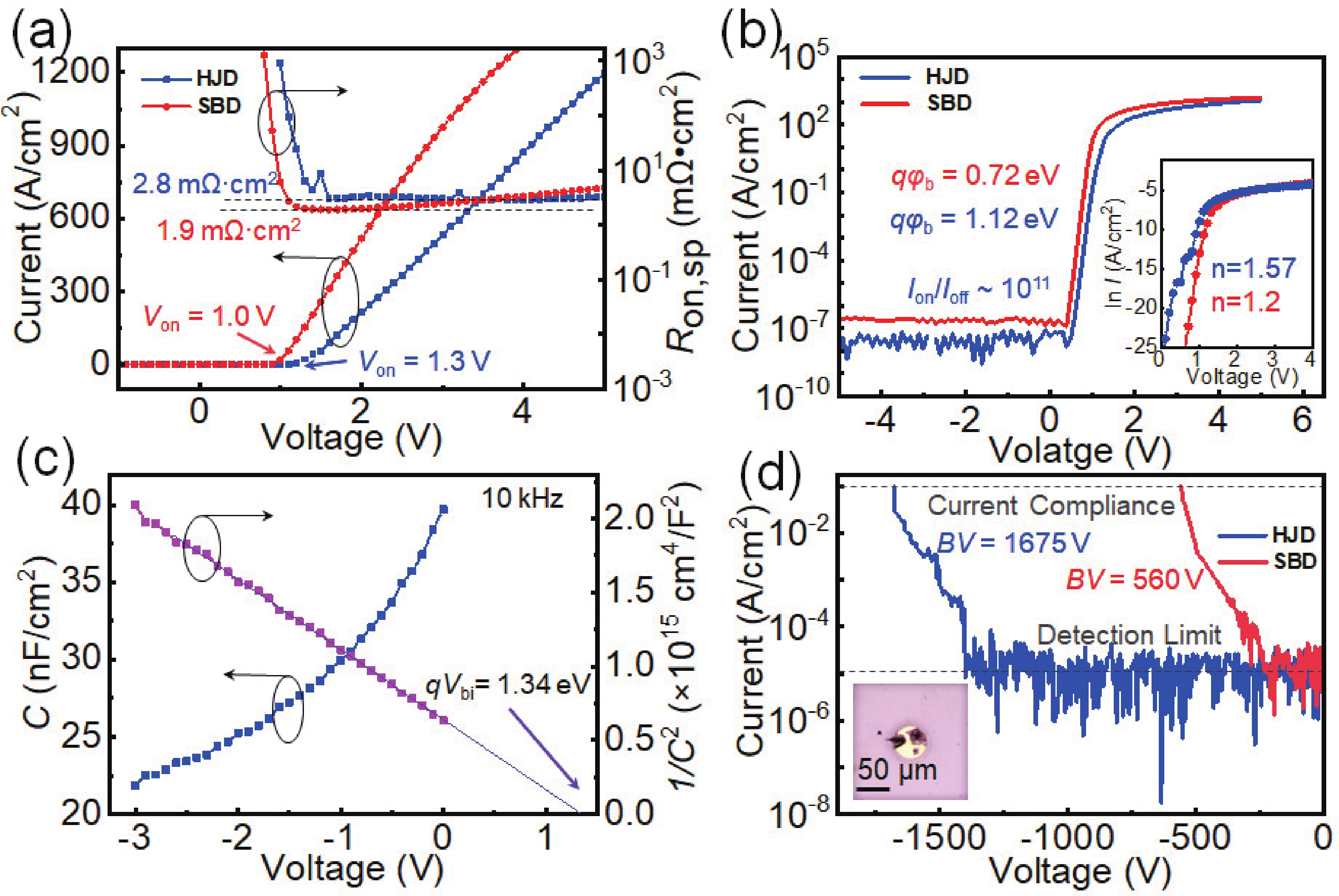
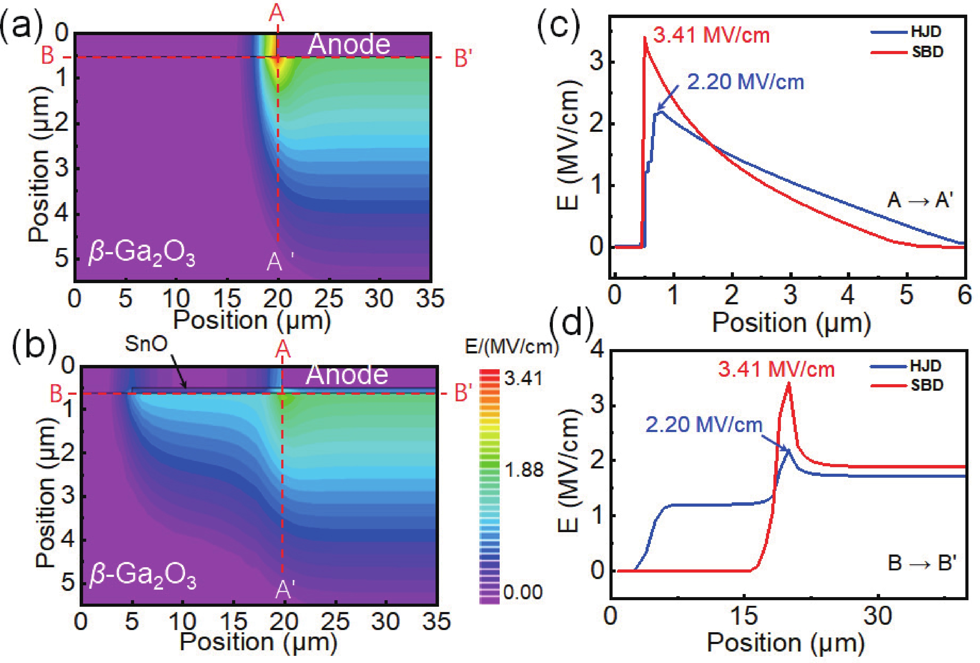
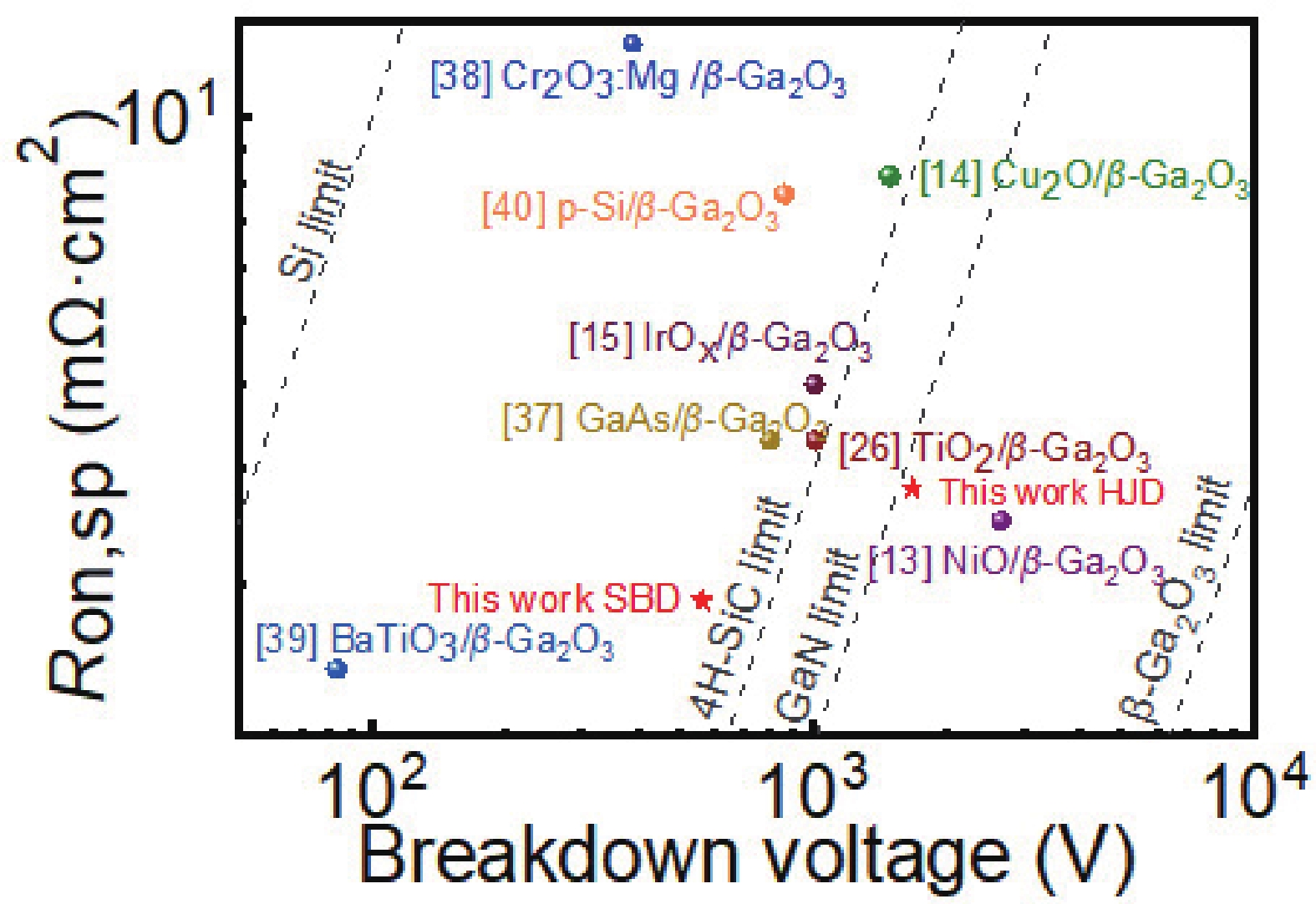
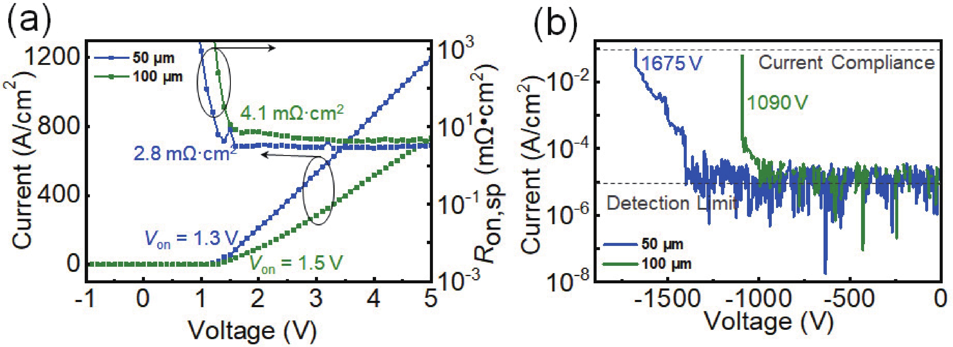
In this study, we present the fabrication of vertical SnO/β-Ga2O3 heterojunction diode (HJD) via radio frequency (RF) reactive magnetron sputtering. The valence and conduction band offsets between β-Ga2O3 and SnO are determined to be 2.65 and 0.75 eV, respectively, through X-ray photoelectron spectroscopy, showing a type-Ⅱ band alignment. Compared to its Schottky barrier diode (SBD) counterpart, the HJD presents a comparable specific ON-resistances (Ron,sp) of 2.8 mΩ·cm² and lower reverse leakage current (IR), leading to an enhanced reverse blocking characteristics with breakdown voltage (BV) of 1675 V and power figure of merit (PFOM) of 1.0 GW/cm². This demonstrates the high quality of the SnO/β-Ga2O3 heterojunction interface. Silvaco TCAD simulation further reveals that electric field crowding at the edge of anode for the SBD was greatly depressed by the introduction of SnO film, revealing the potential application of SnO/β-Ga2O3 heterojunction in the future β-Ga2O3-based power devices.
J. Semicond.
2025, 46(8): 082801 doi: 10.1088/1674-4926/25010027
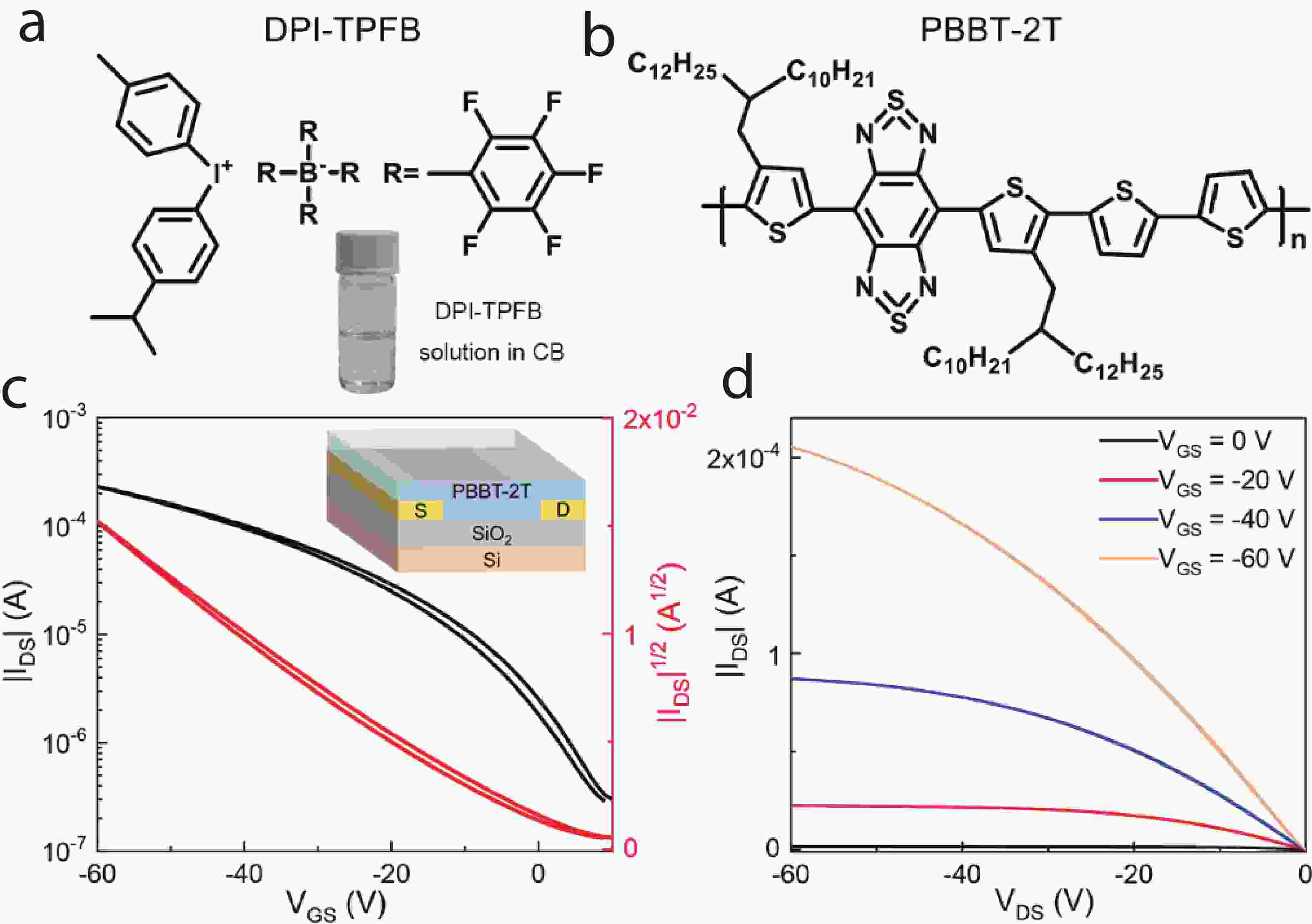
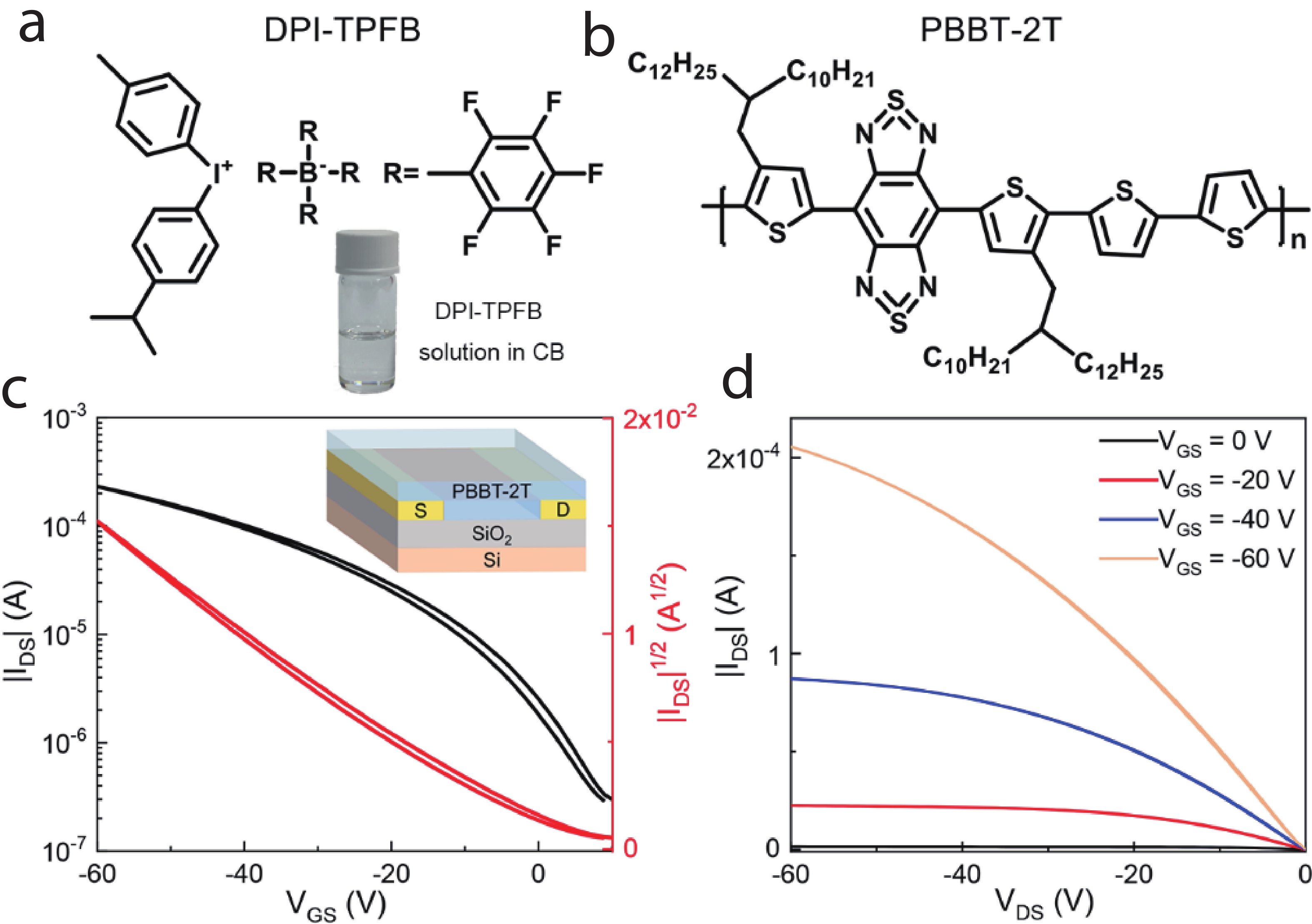
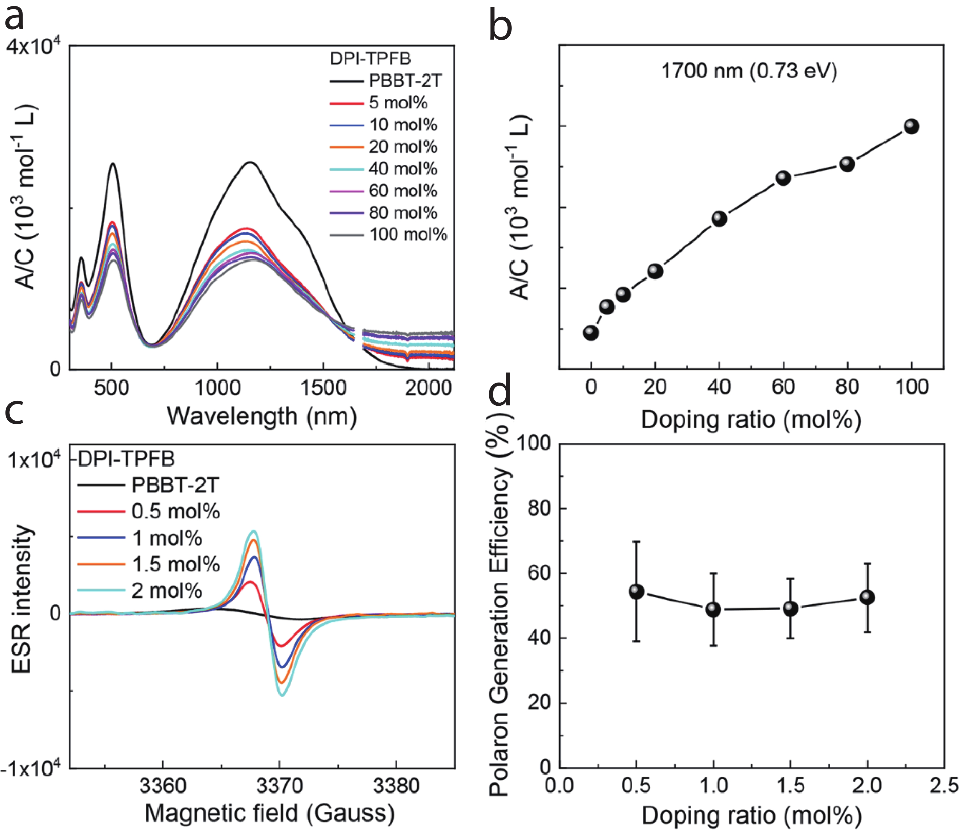
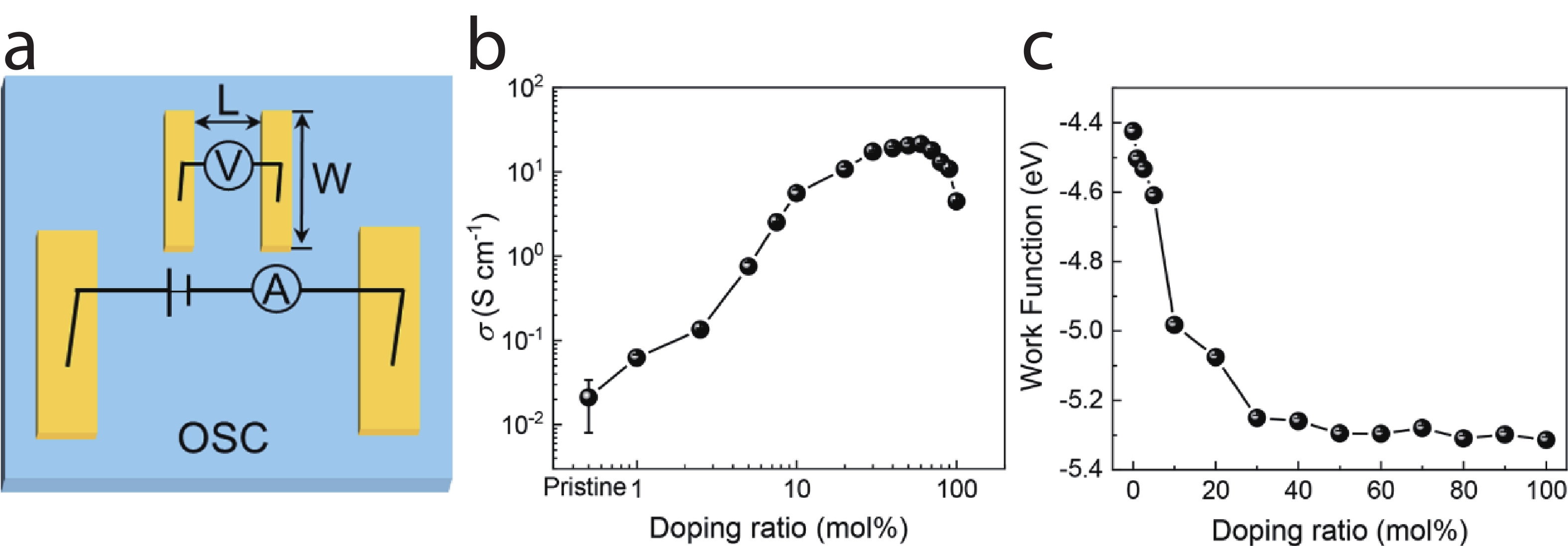
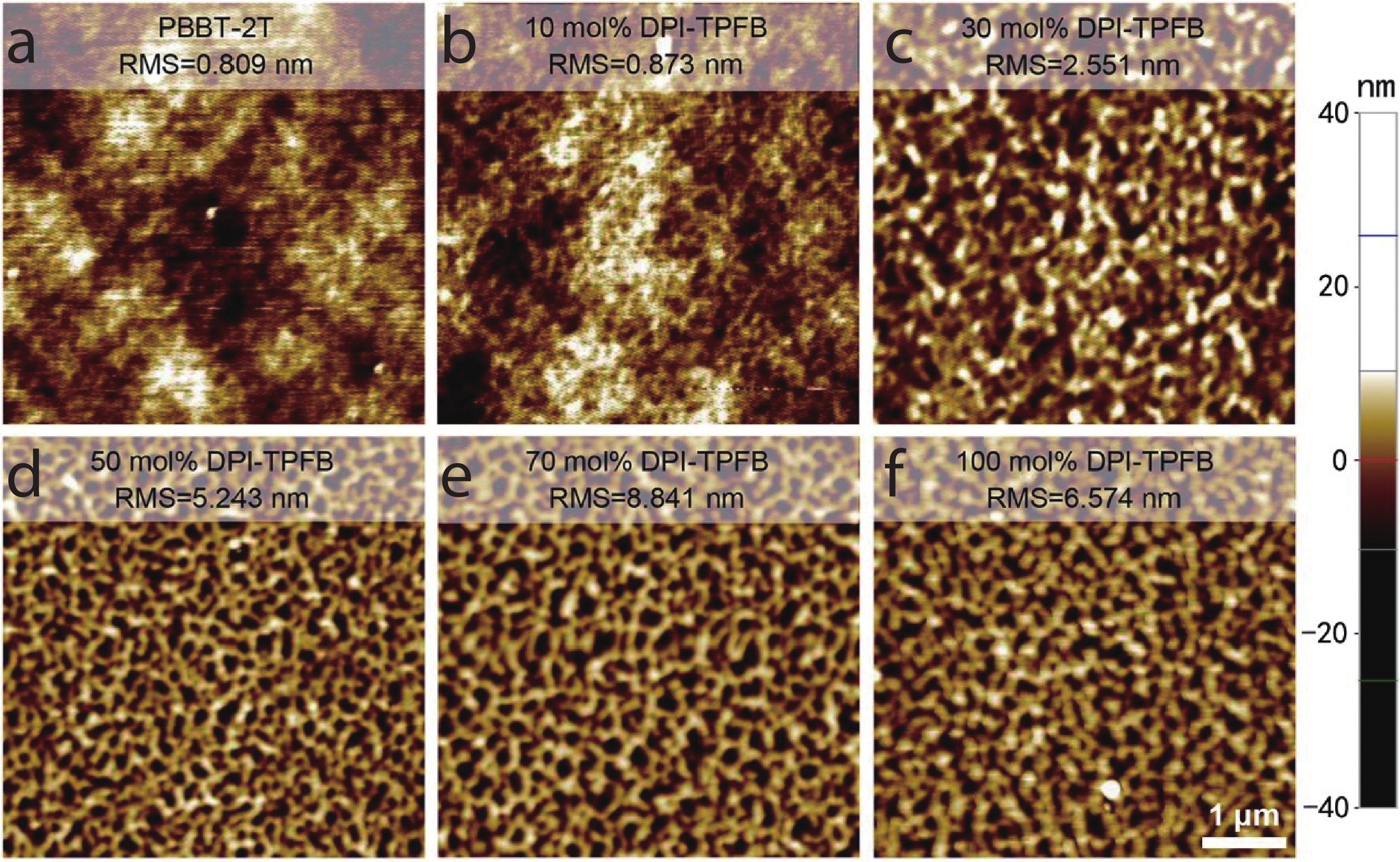
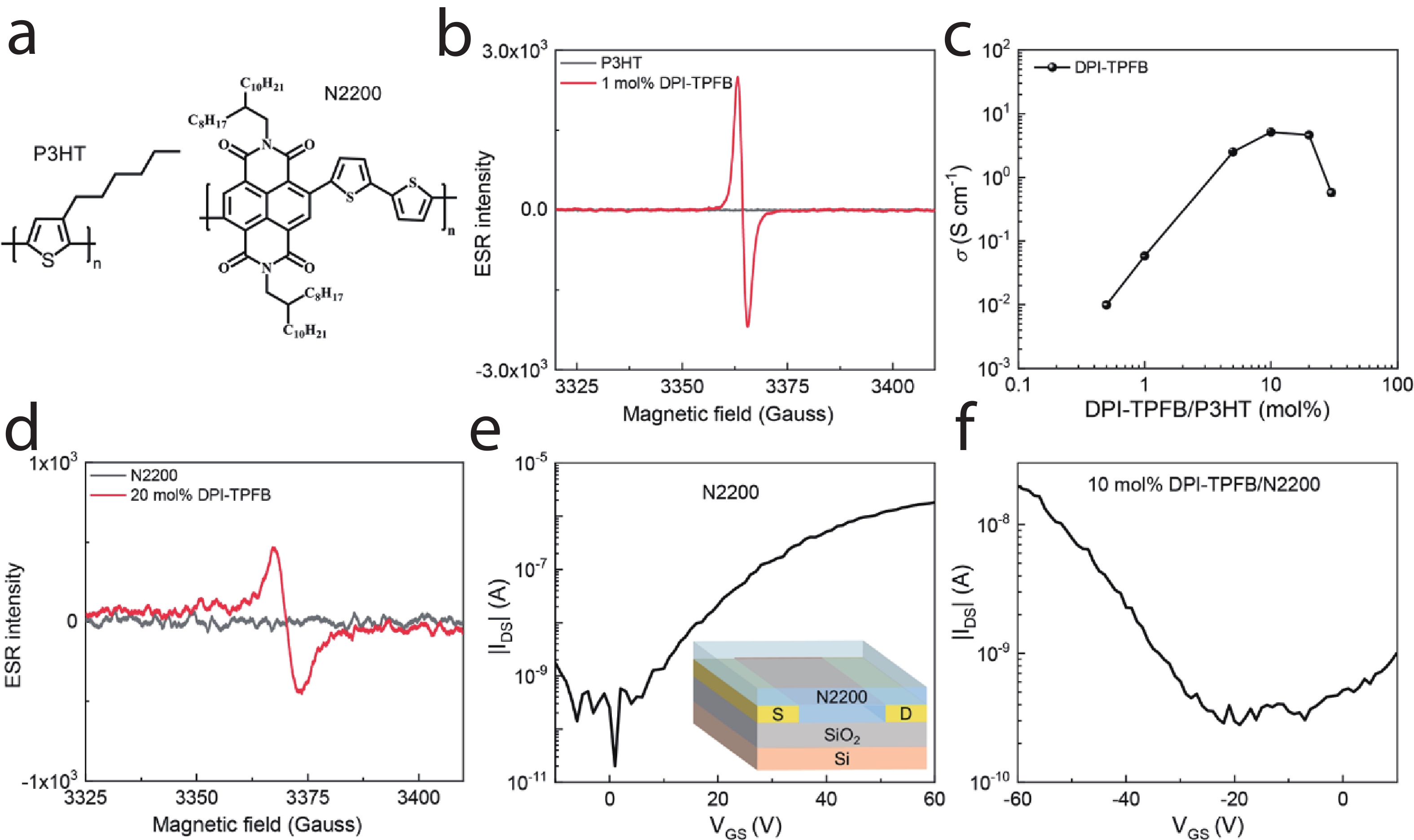
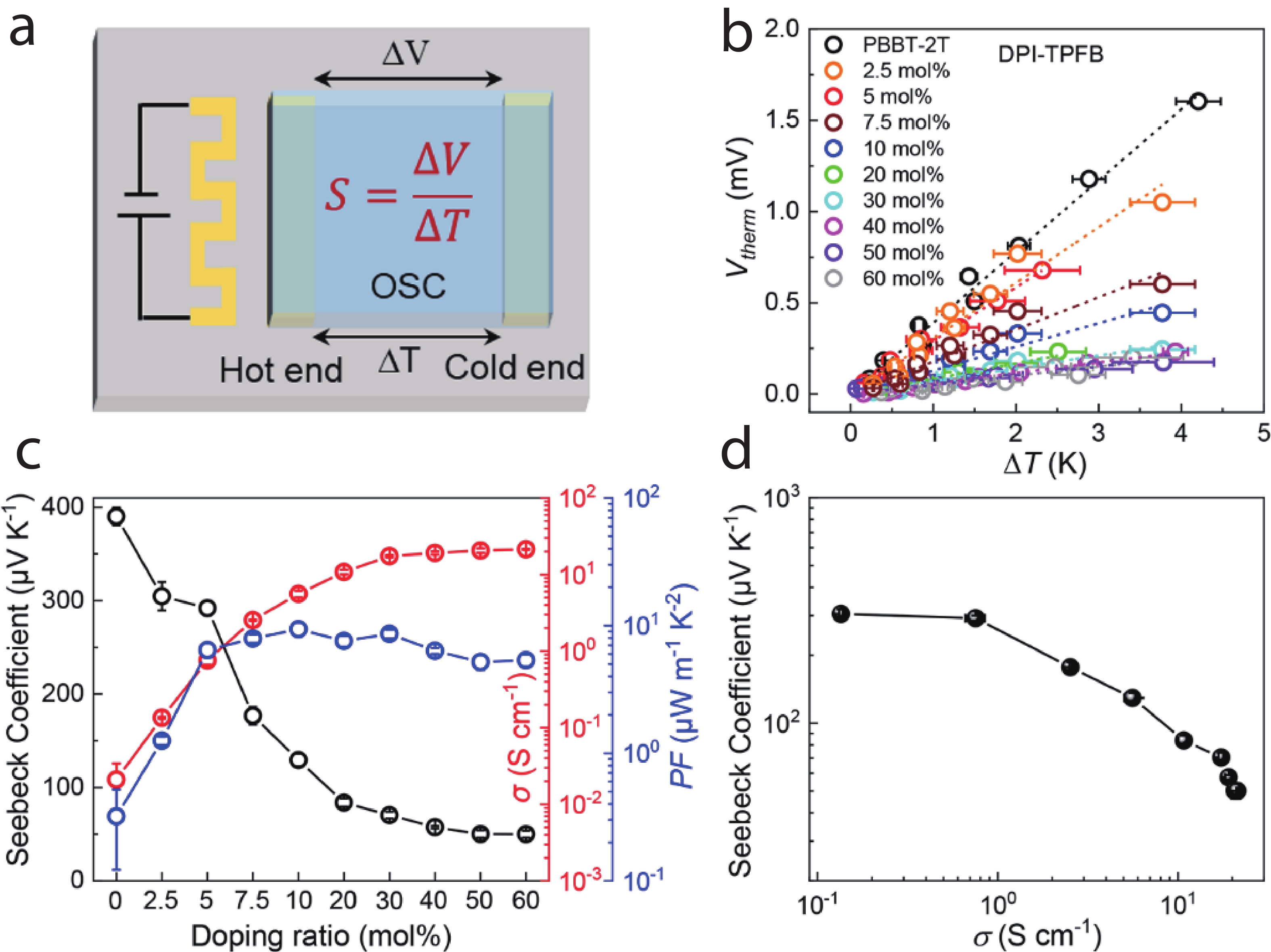
Doping plays a pivotal role in enhancing the performance of organic semiconductors (OSCs) for advanced optoelectronic and thermoelectric applications. In this study, we systematically investigated the doping performance and applicability of the ionic dopant 4-isopropyl-4′-methyldiphenyliodonium tetrakis(penta-fluorophenyl-borate) (DPI-TPFB) as a p-dopant for OSCs. Using the p-type OSC PBBT-2T as a model system, we demonstrated that DPI-TPFB shows significant doping effect, as confirmed by ESR spectra, ultraviolet−visible−near-infrared (UV−vis−NIR) absorption, and work function analysis, and enhances the electronic conductivity of PBBT-2T films by over four orders of magnitude. Furthermore, DPI-TPFB exhibited broad doping applicability, effectively doping various p-type OSCs and even imparting p-type characteristics to the n-type OSC N2200, transforming its intrinsic n-type behavior into p-type. The application of DPI-TPFB-doped PBBT-2T films in organic thermoelectric devices (OTEs) was also explored, achieving a power factor of approximately 10 μW∙m−1∙K−2. These findings highlight the potential of DPI-TPFB as a versatile and efficient dopant for integration into organic optoelectronic and thermoelectric devices.