Issue Browser
Volume 46, Issue 6,
Jun 2025
J. Semicond.
2025, 46(6): 062201 doi: 10.1088/1674-4926/25010002
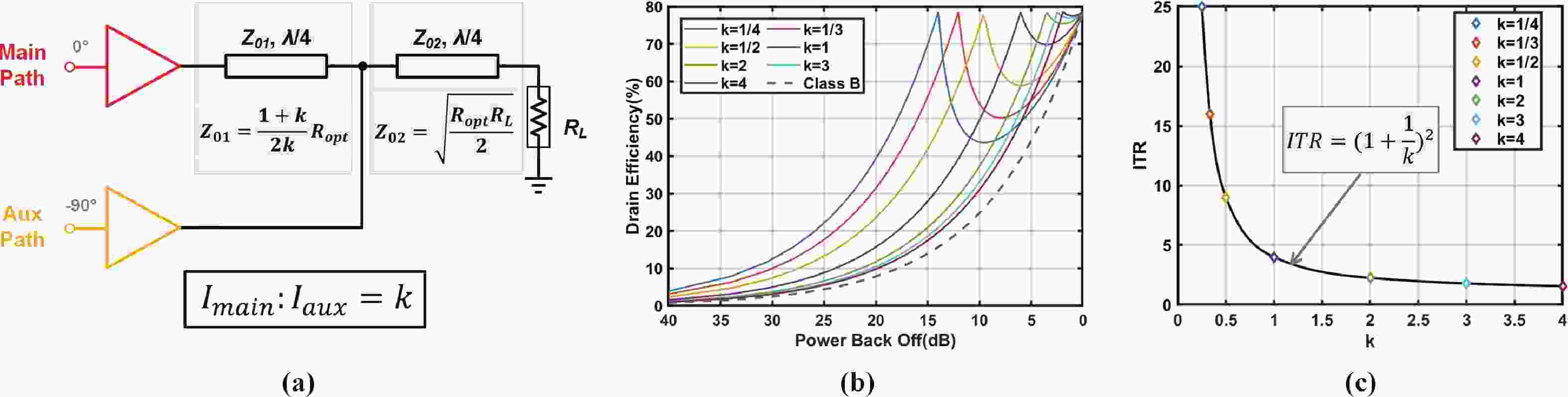
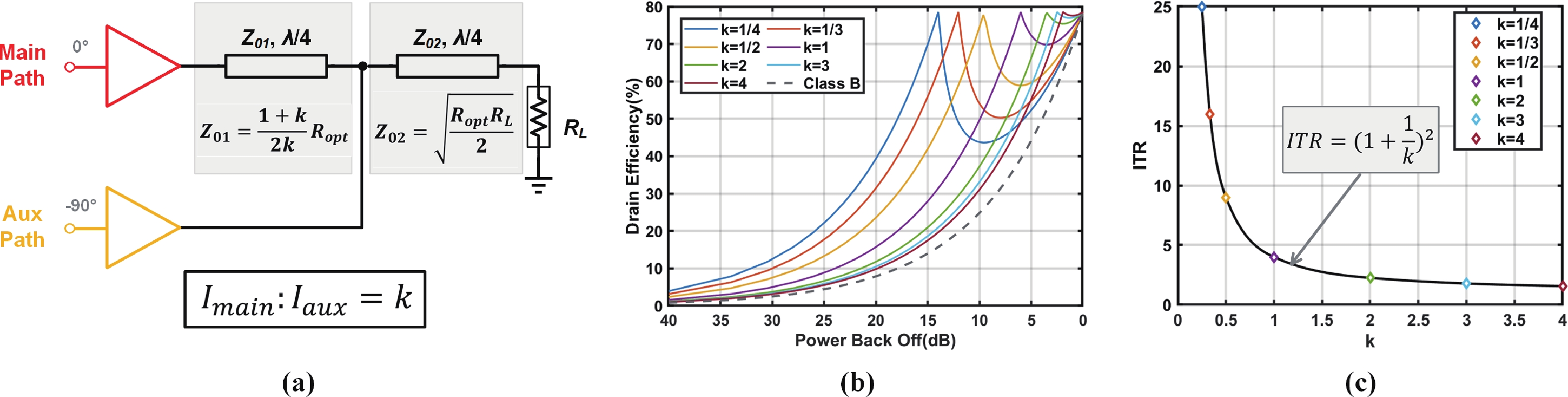
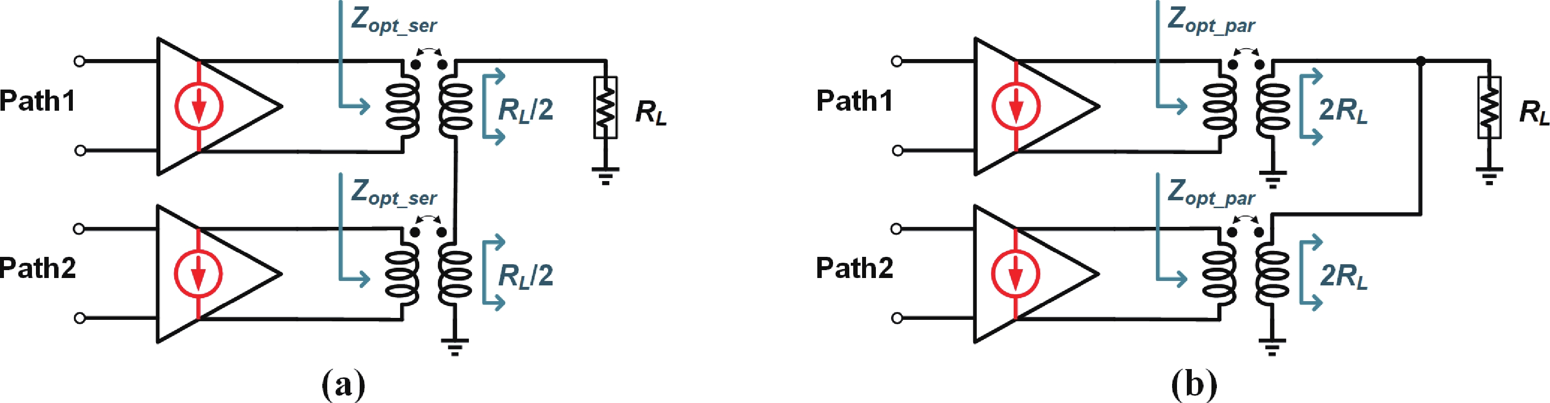
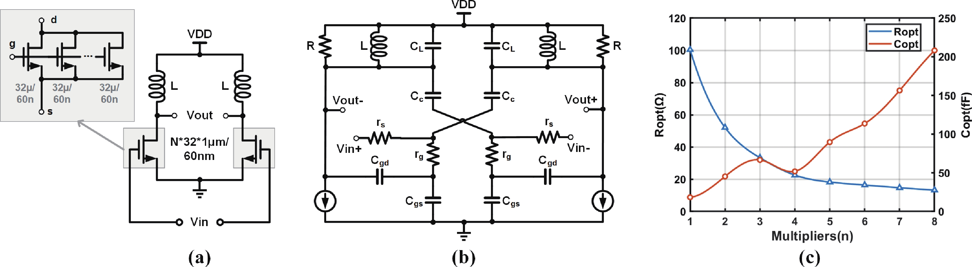
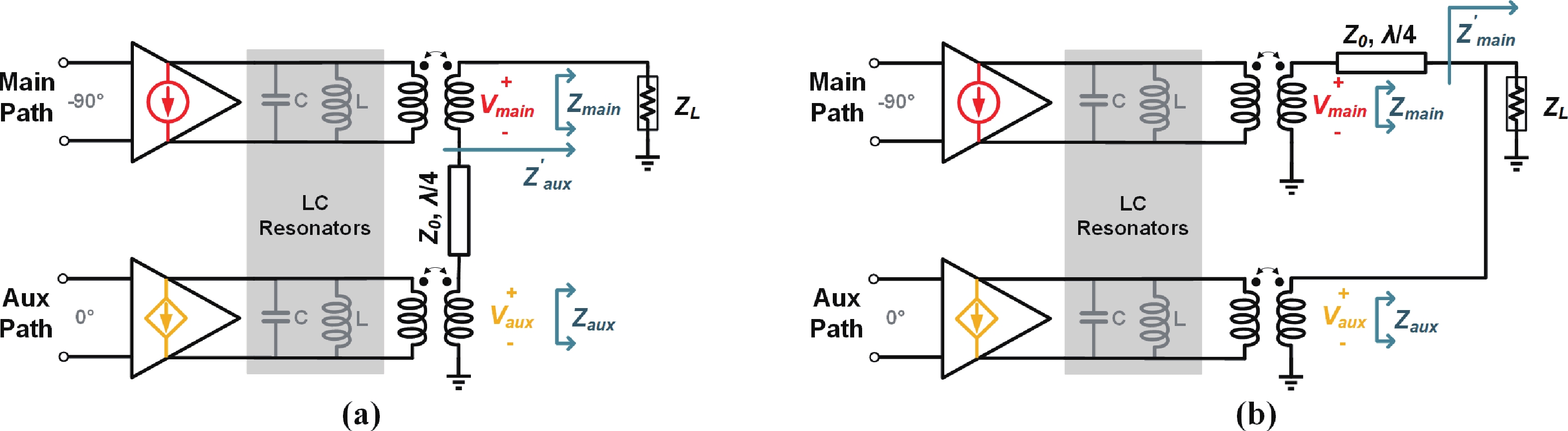
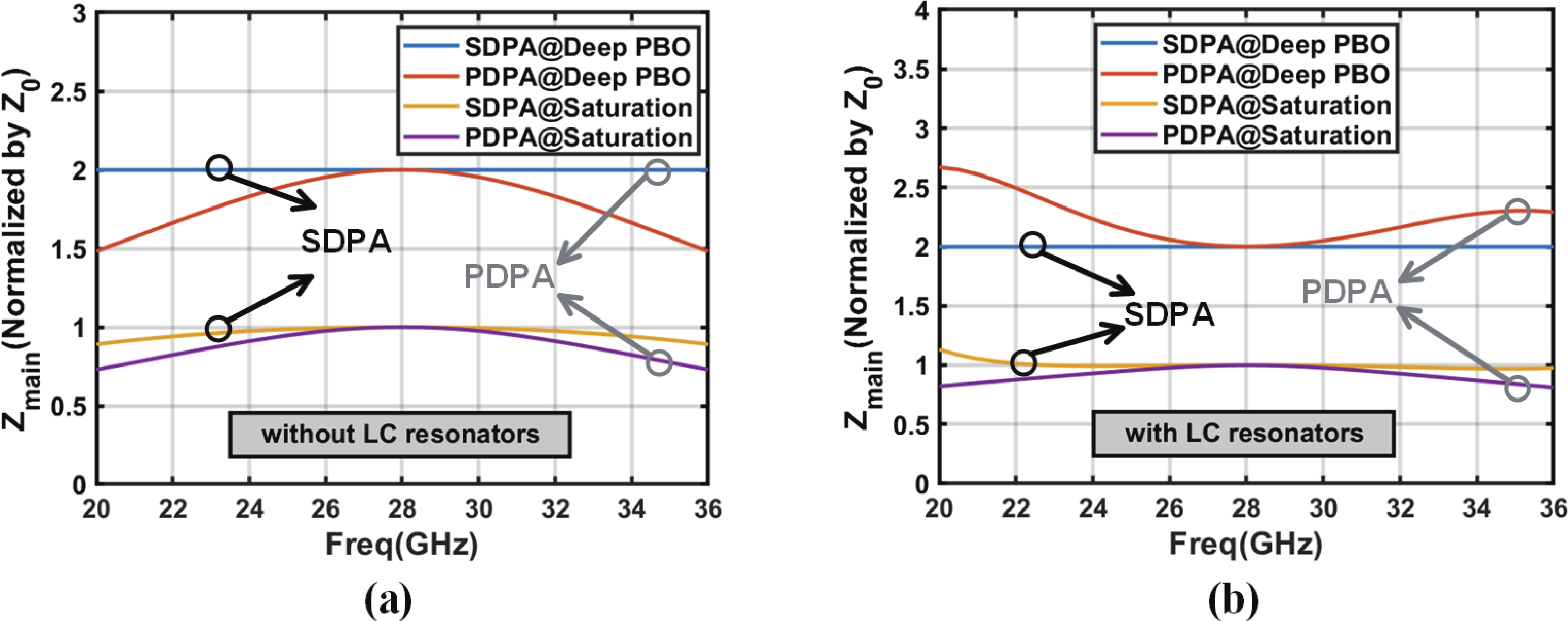
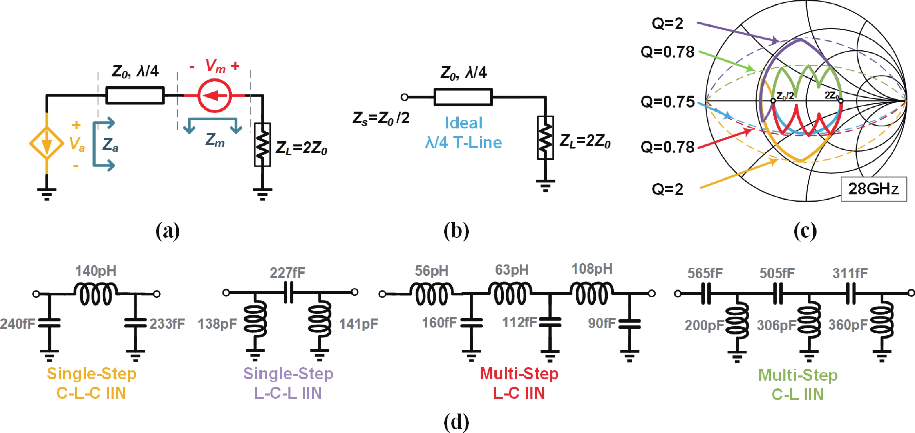
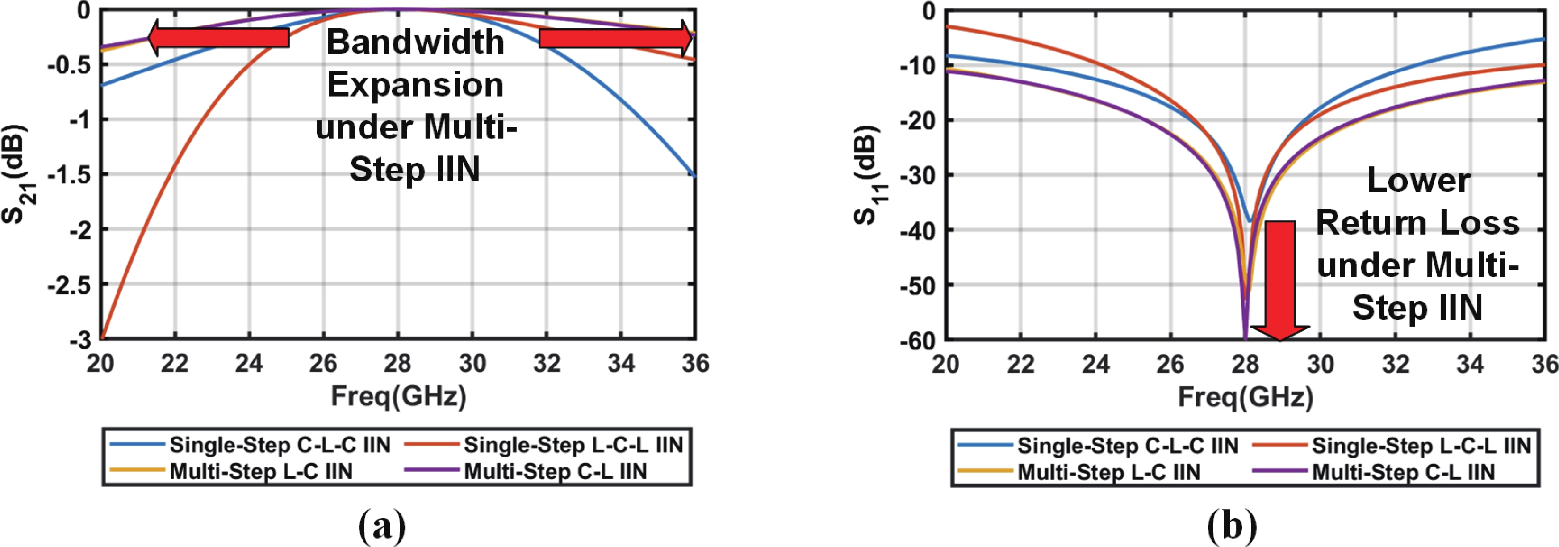
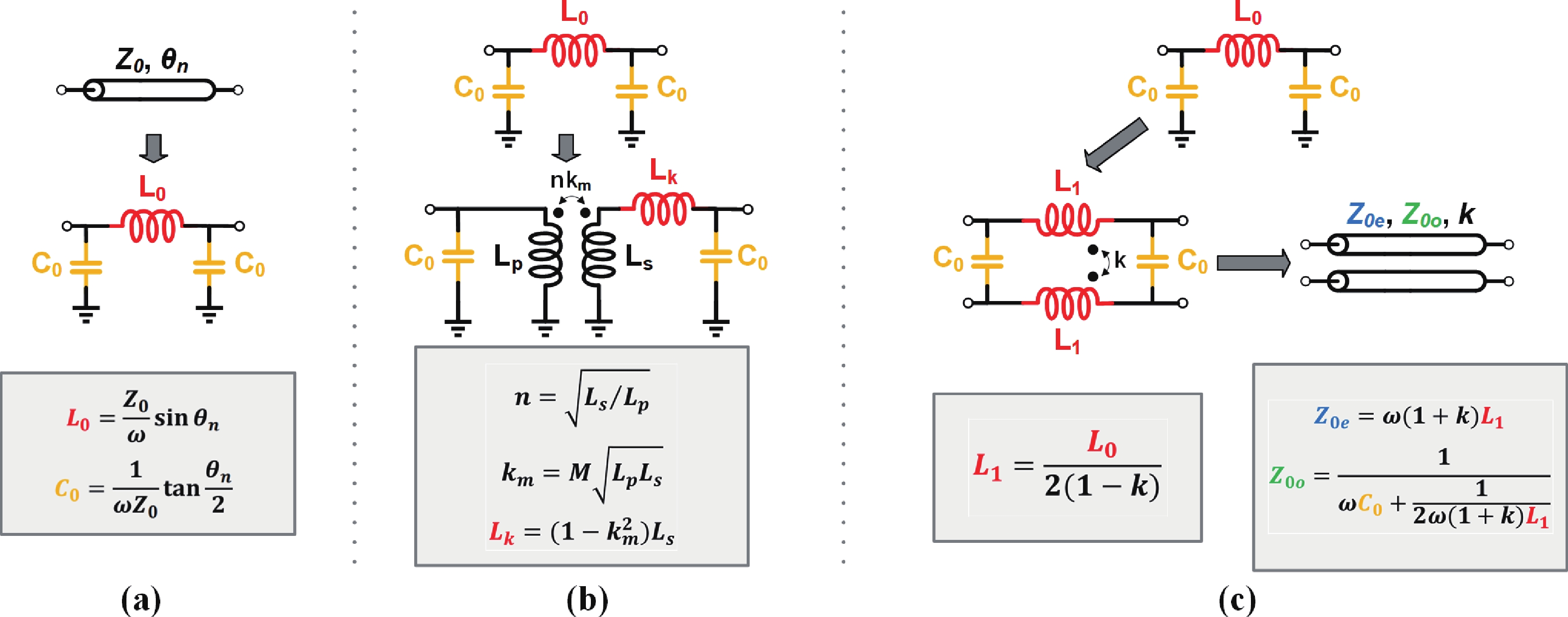
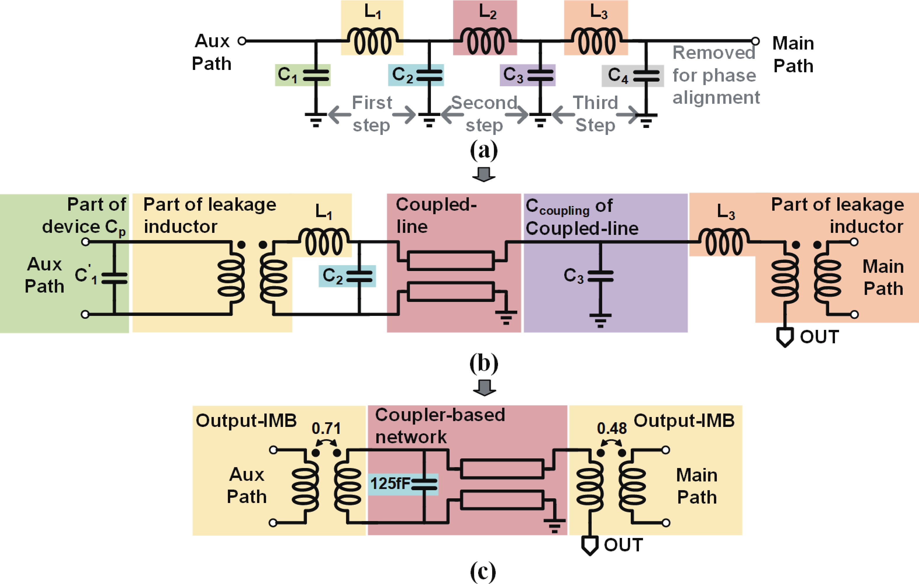
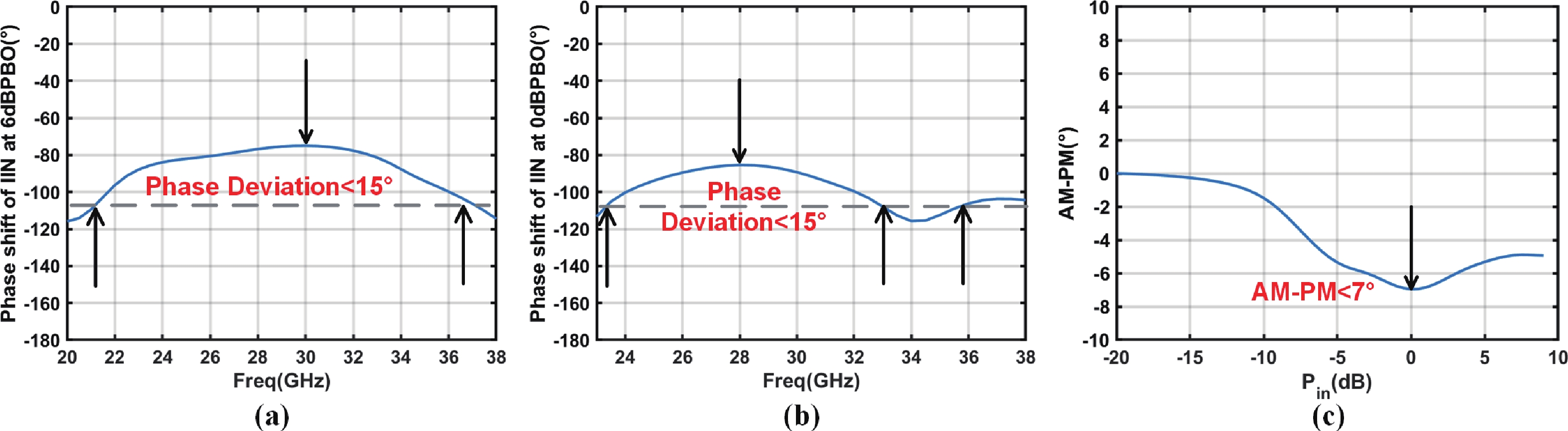
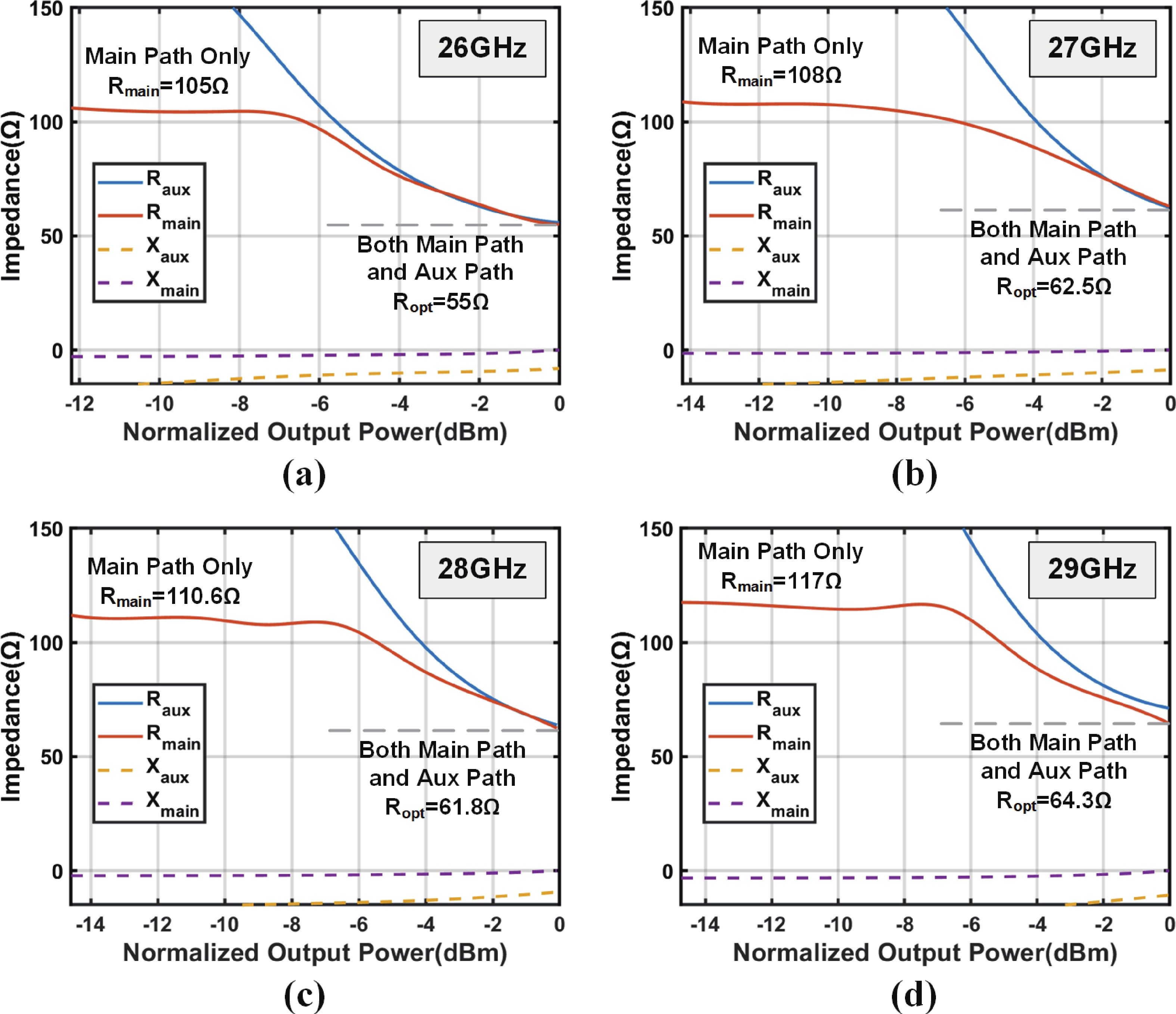
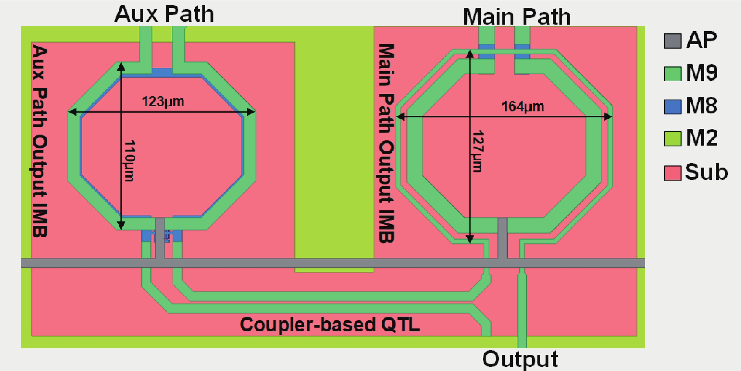
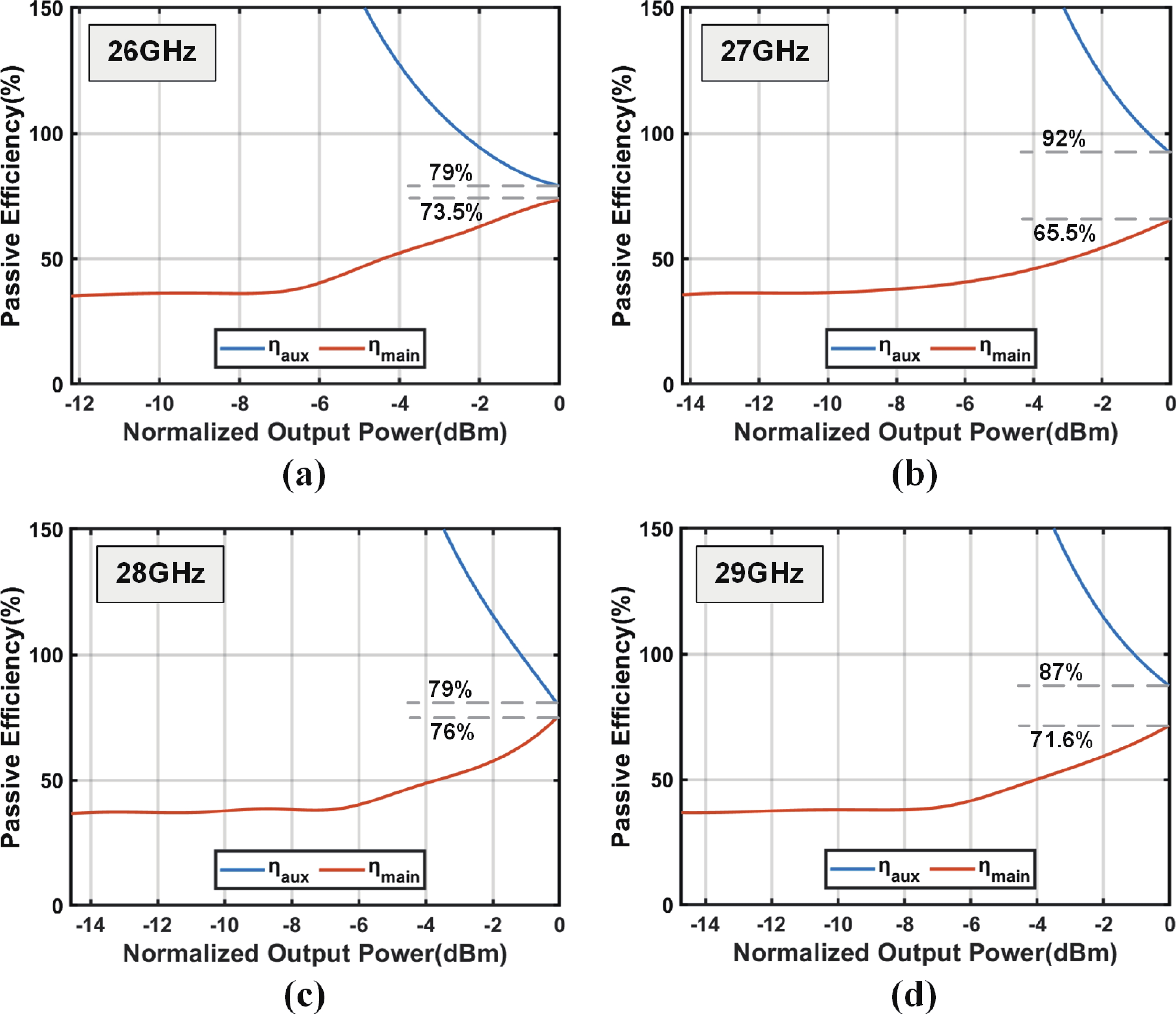
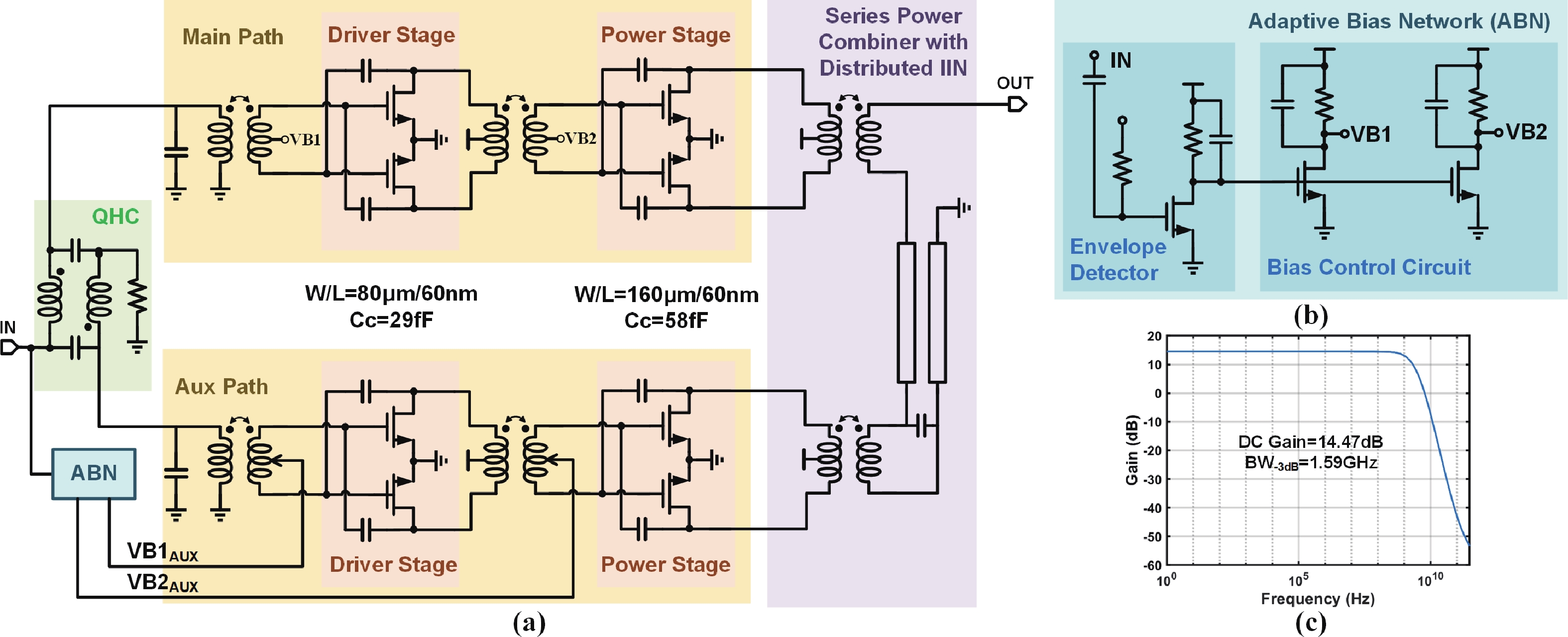
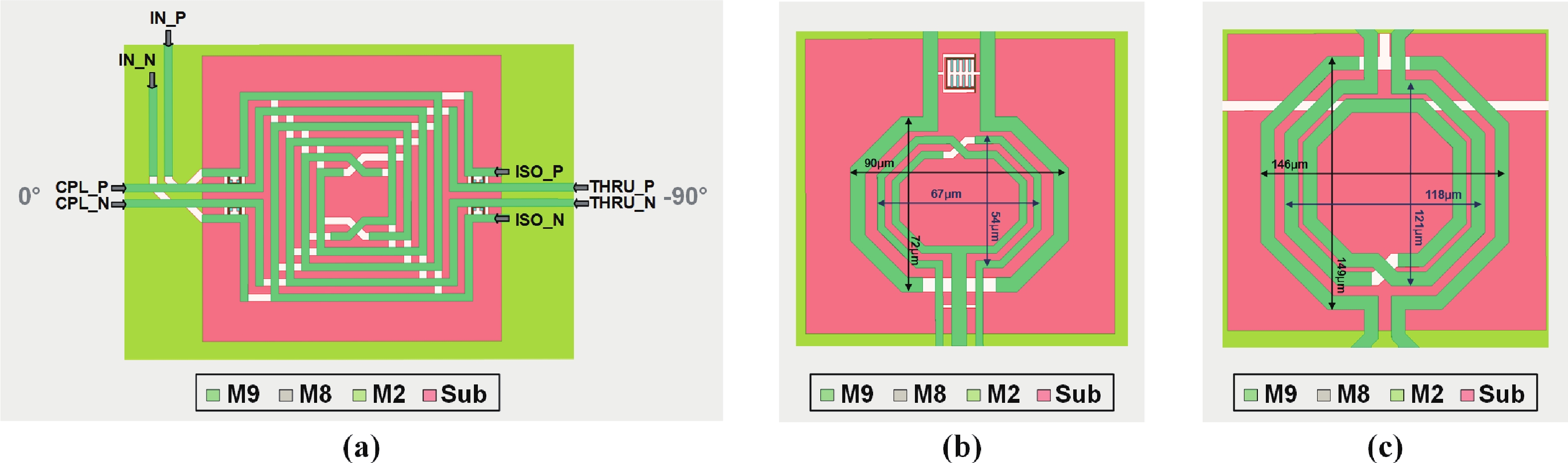
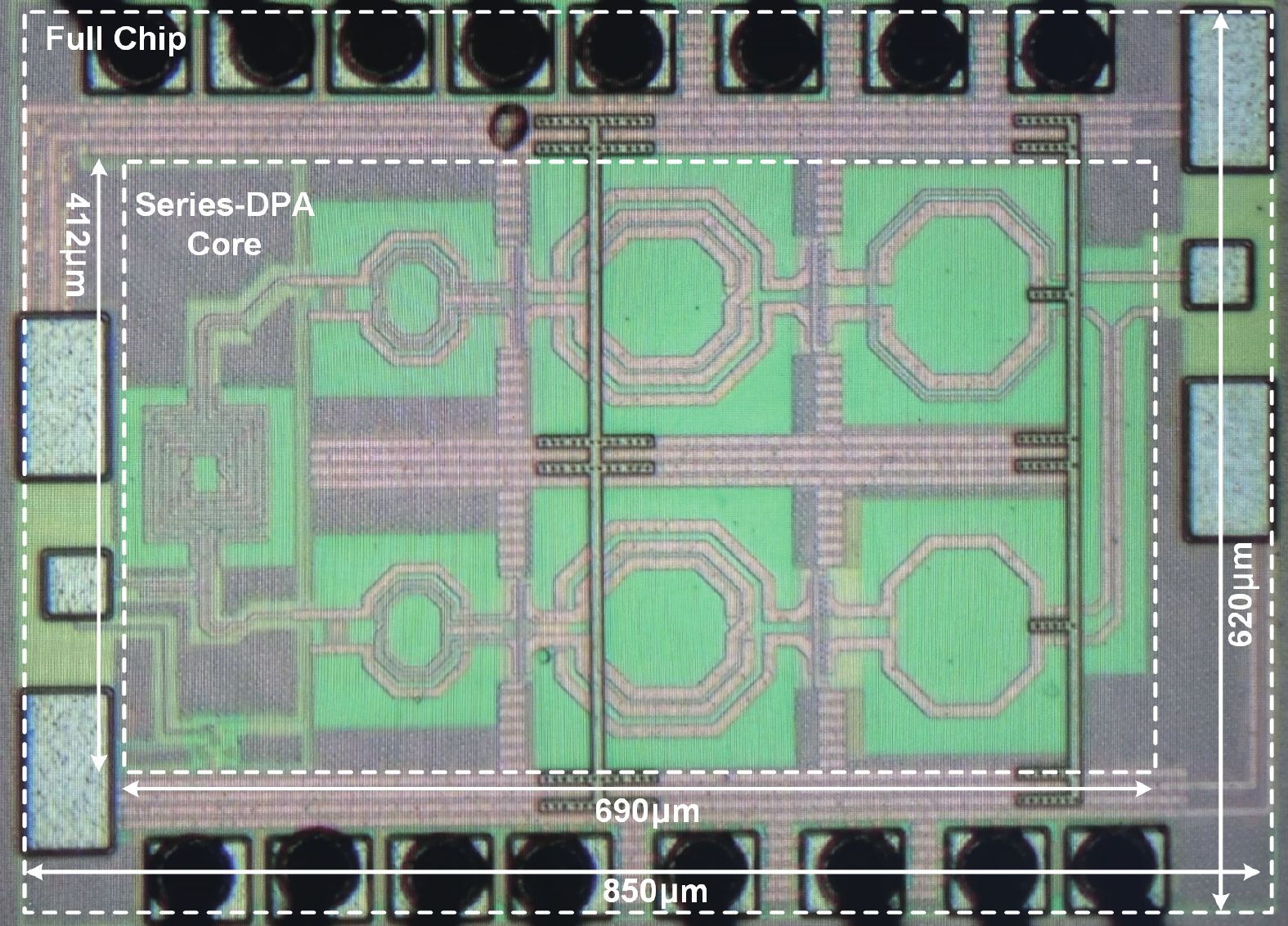
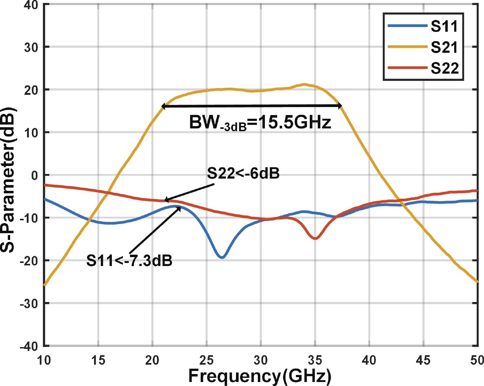
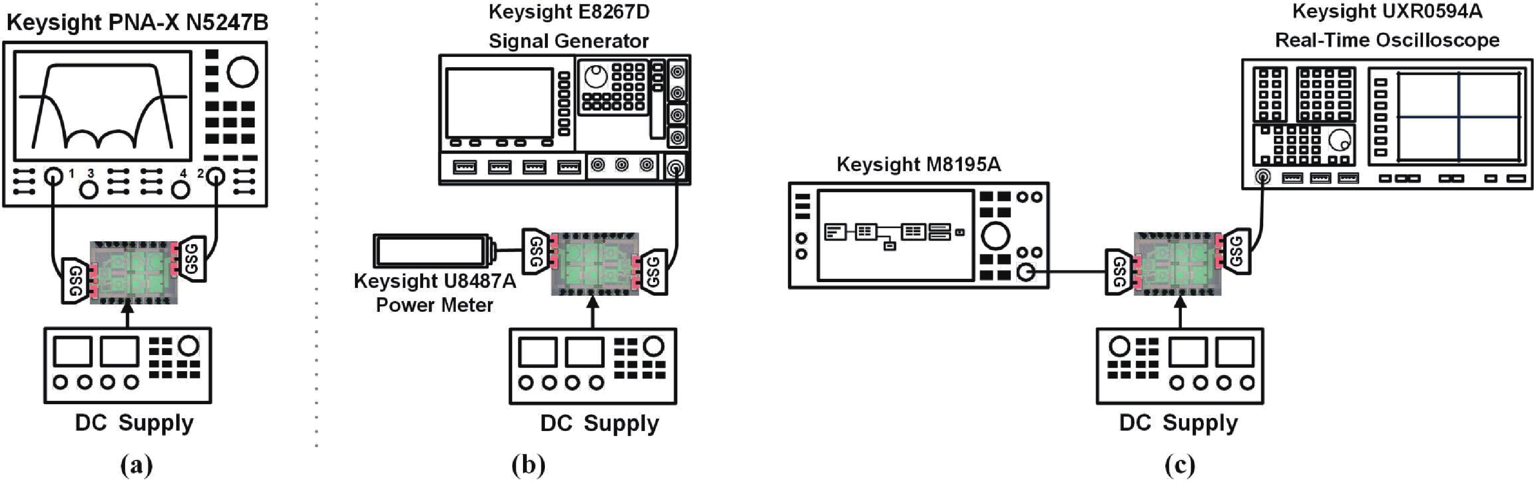
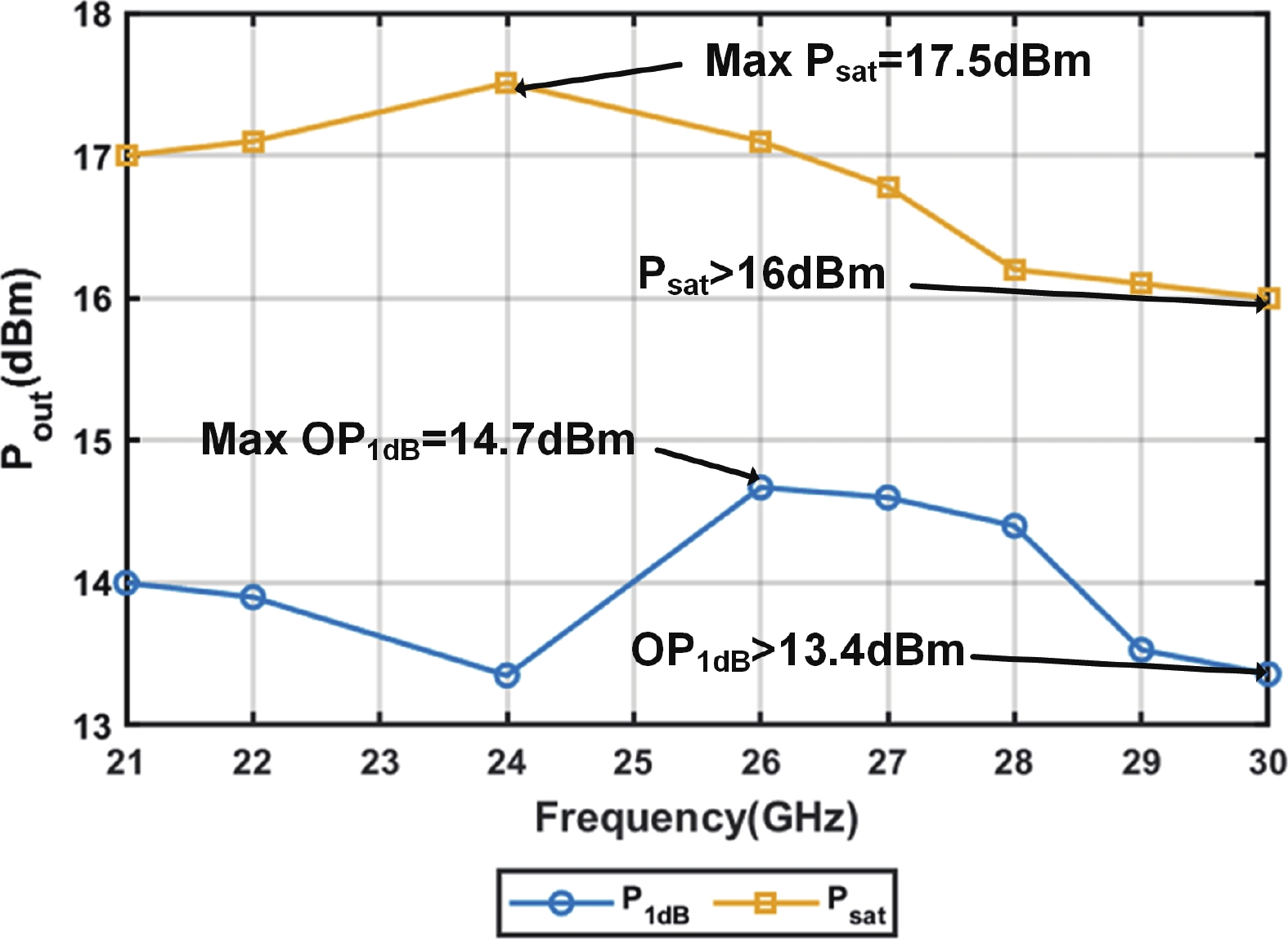
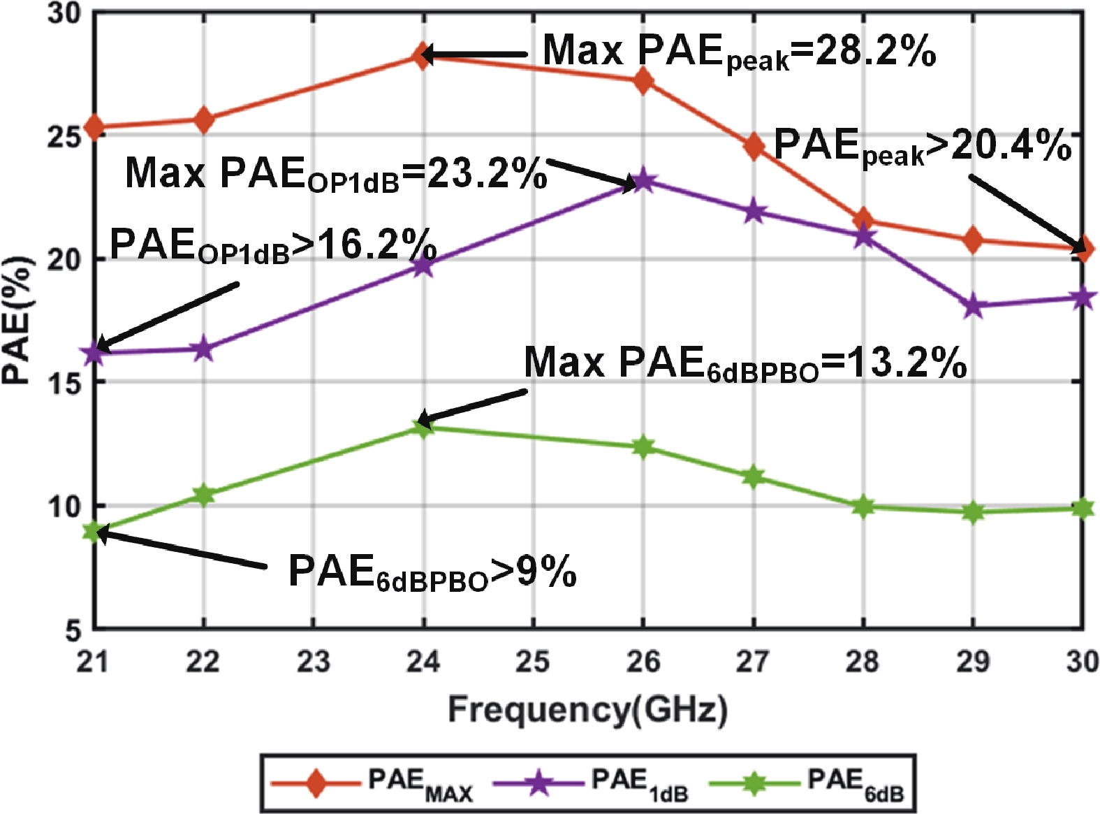
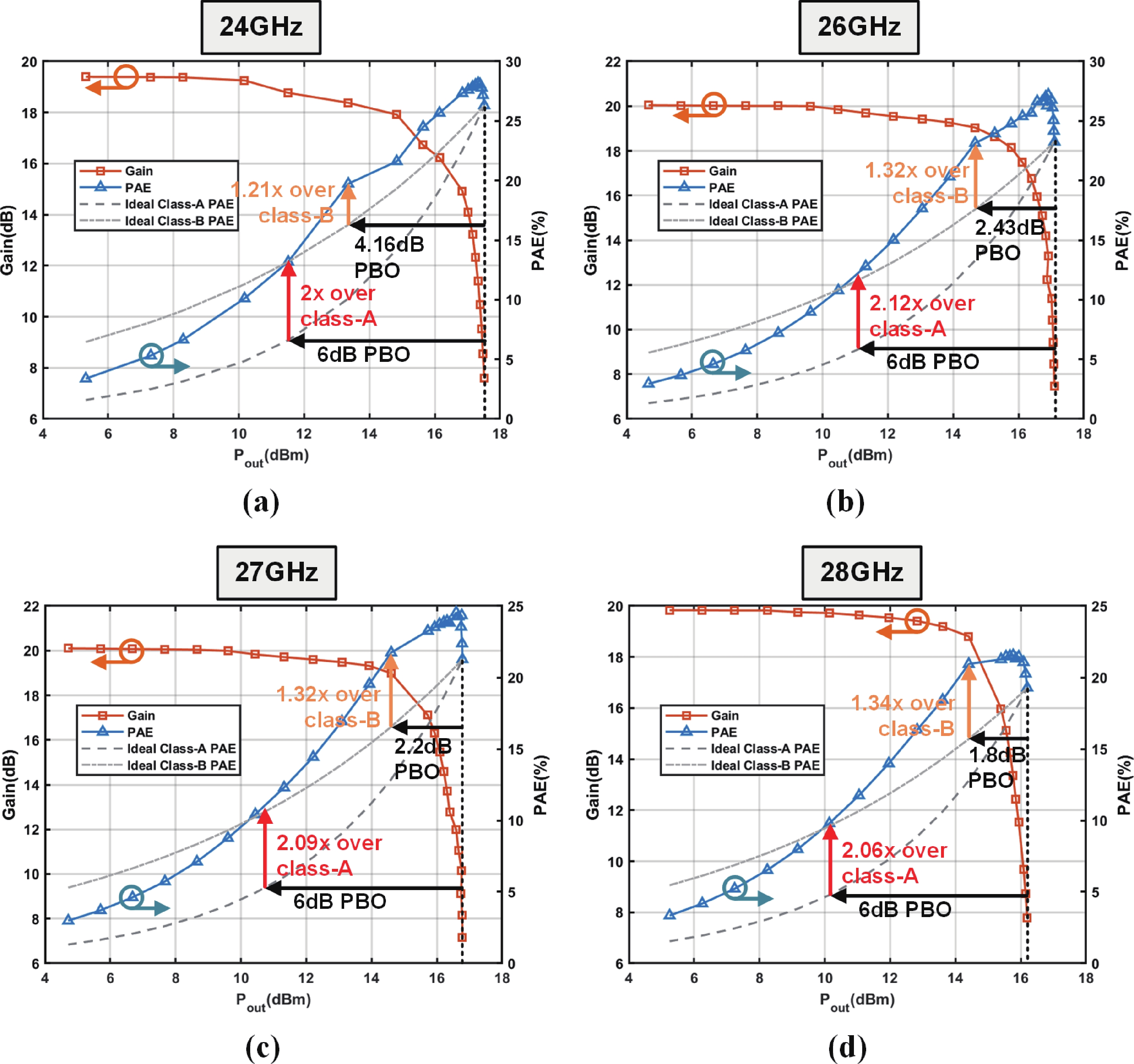
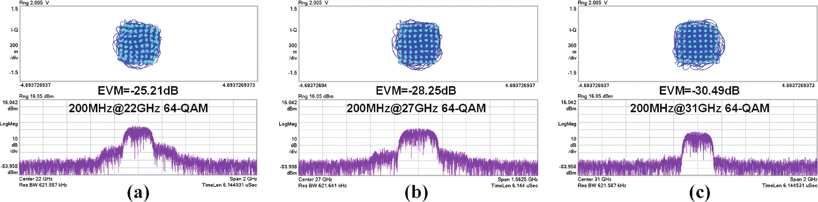
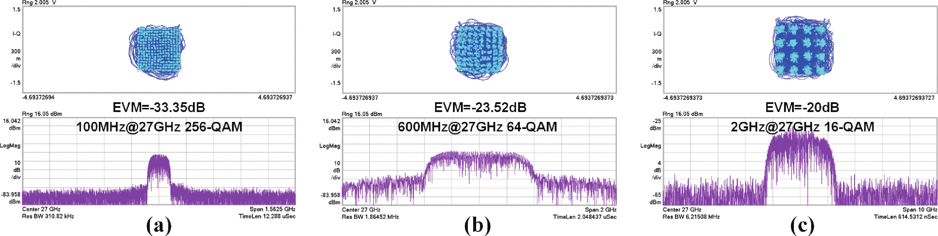
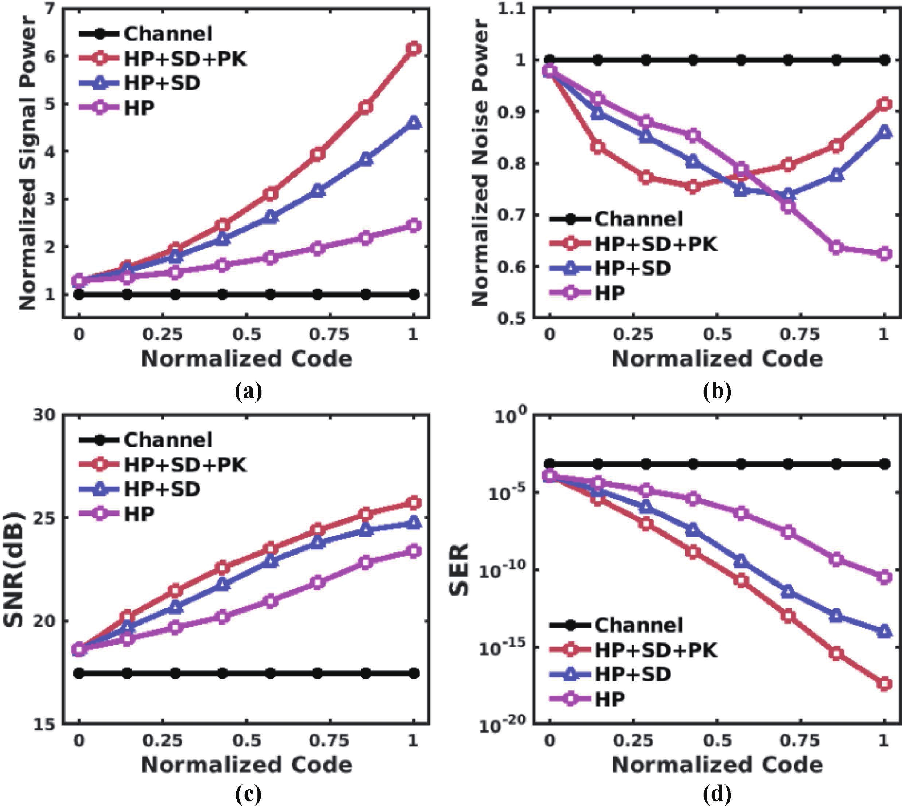
A two-way K/Ka-band series-Doherty PA (SDPA) with a distributed impedance inverting network (IIN) for millimeter wave applications is presented in this article. The proposed distributed IIN contributes to achieve wideband linear and power back-off (PBO) efficiency enhancement. Implemented in 65 nm bulk CMOS technology, this work realizes a measured 3 dB bandwidth of 15.5 GHz with 21.2 dB peak small-signal gain at 34.2 GHz. Under 1-V power supply, it achieves OP1dB over 13.4 dBm and Psat over 16 dBm between 21 to 30 GHz. The measured maximum Psat, OP1dB, peak/OP1dB/6dBPBO PAE results are 17.5, 14.7 dBm, and 28.2%/23.2%/13.2%. Without digital pre-distortion (DPD) and equalization, EVMs are lower than −25.2 dB for 200 MHz 64-QAM signals. Besides, this work achieves −33.35, −23.52, and −20 dB EVMs for 100 MHz 256-QAM, 600 MHz 64-QAM and 2 GHz 16-QAM signals at 27 GHz without DPD and equalization.
J. Semicond.
2025, 46(6): 062202 doi: 10.1088/1674-4926/25010028
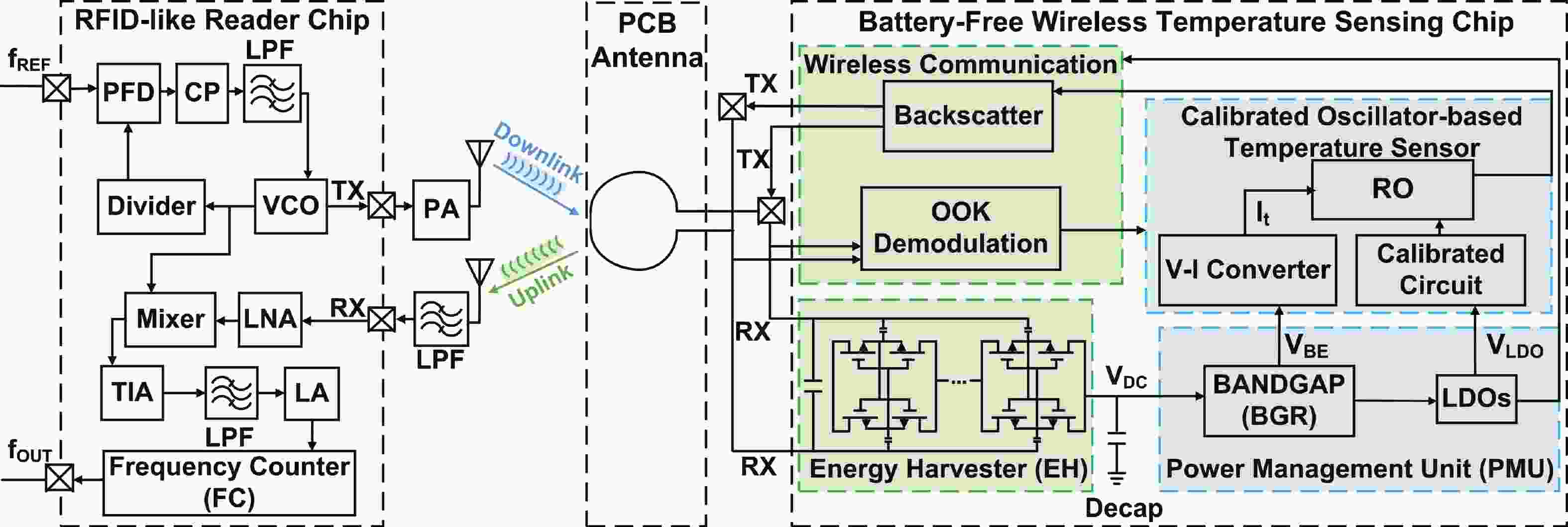
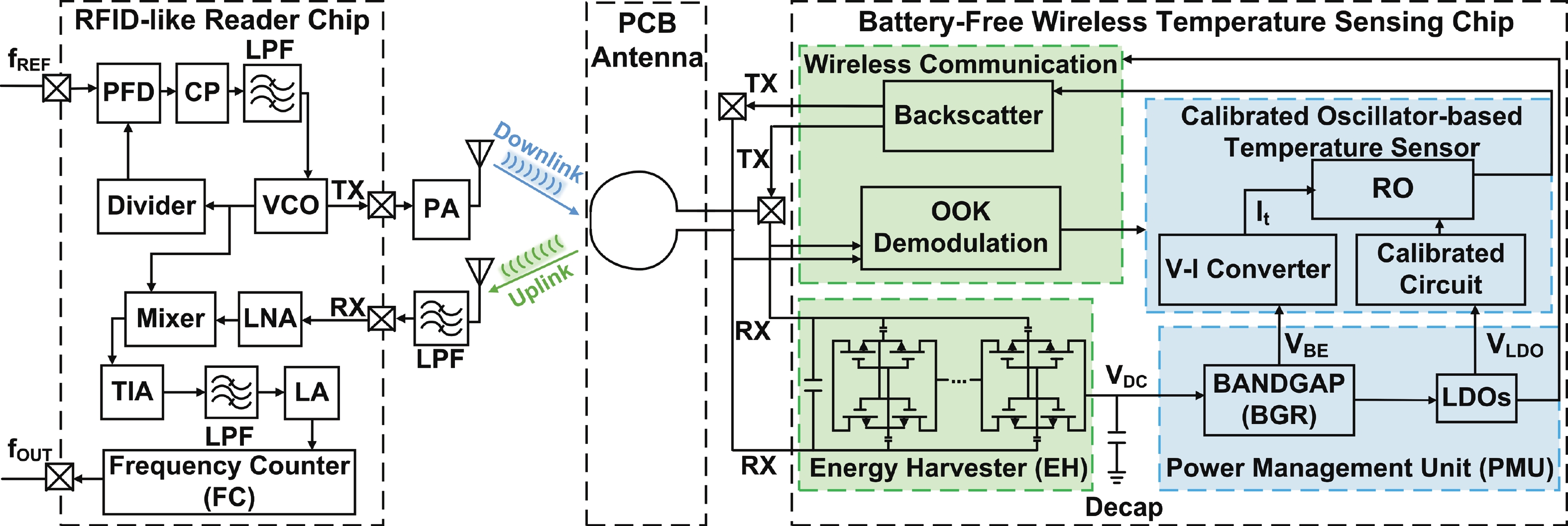
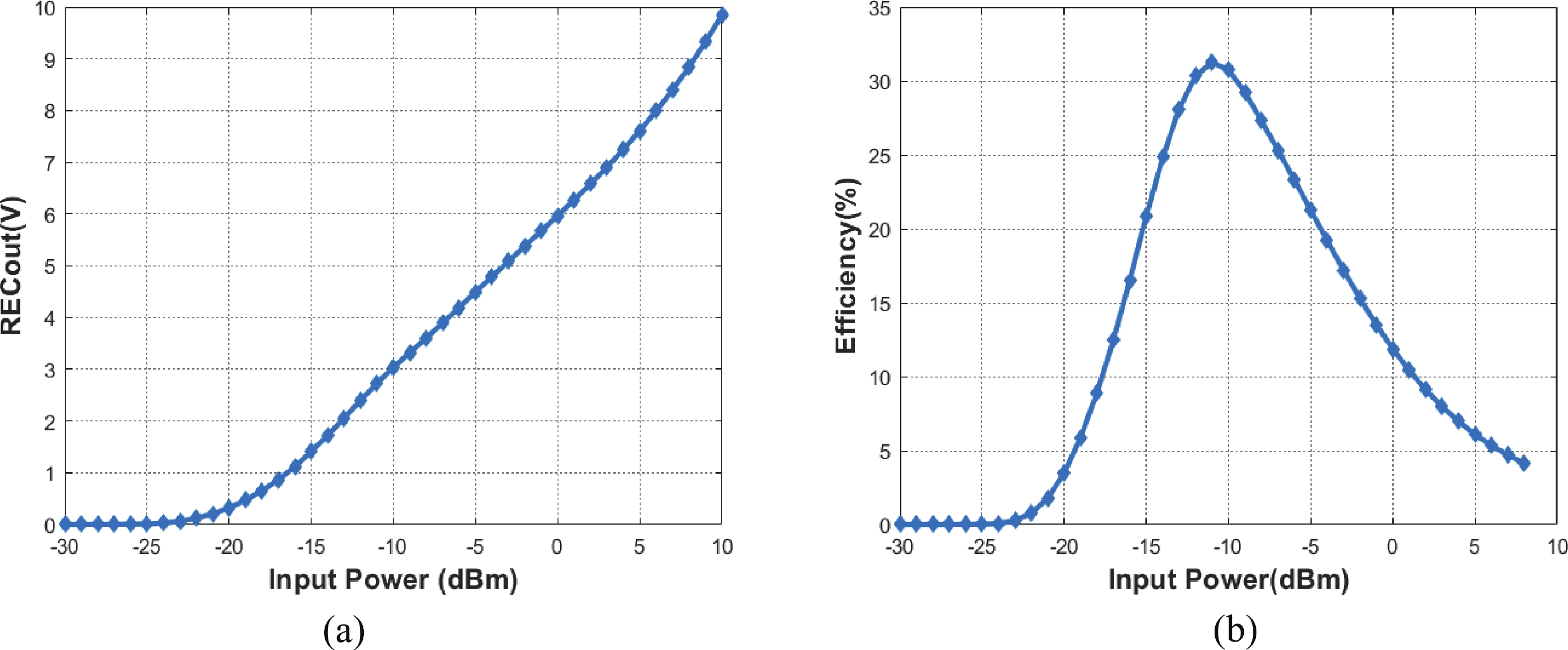
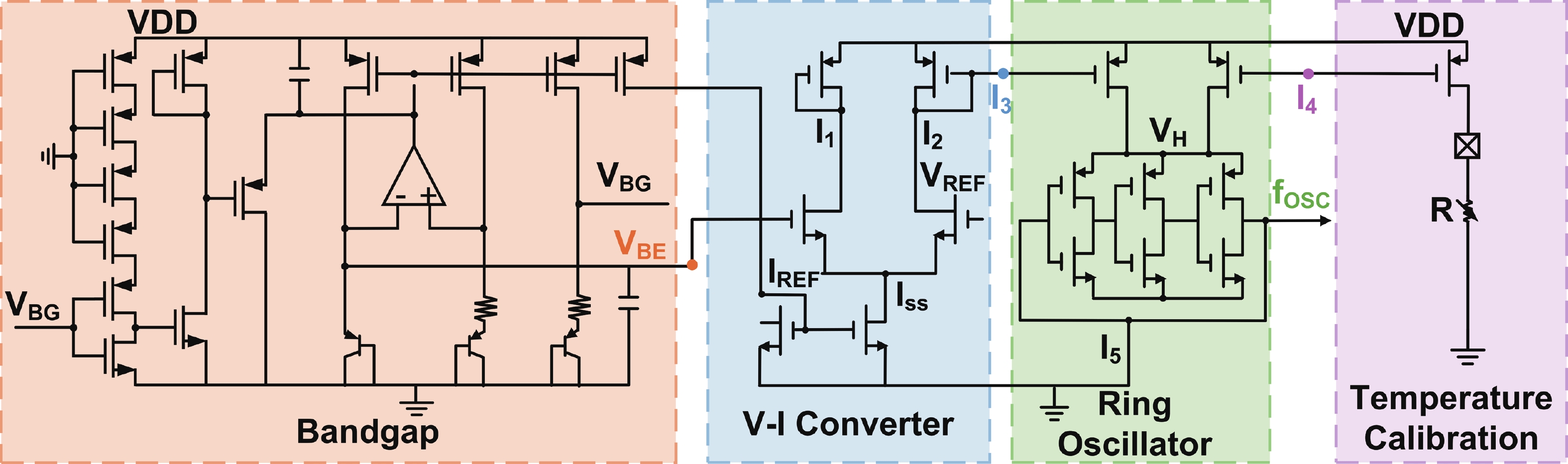
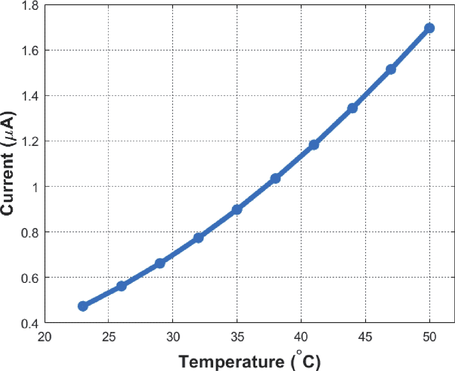
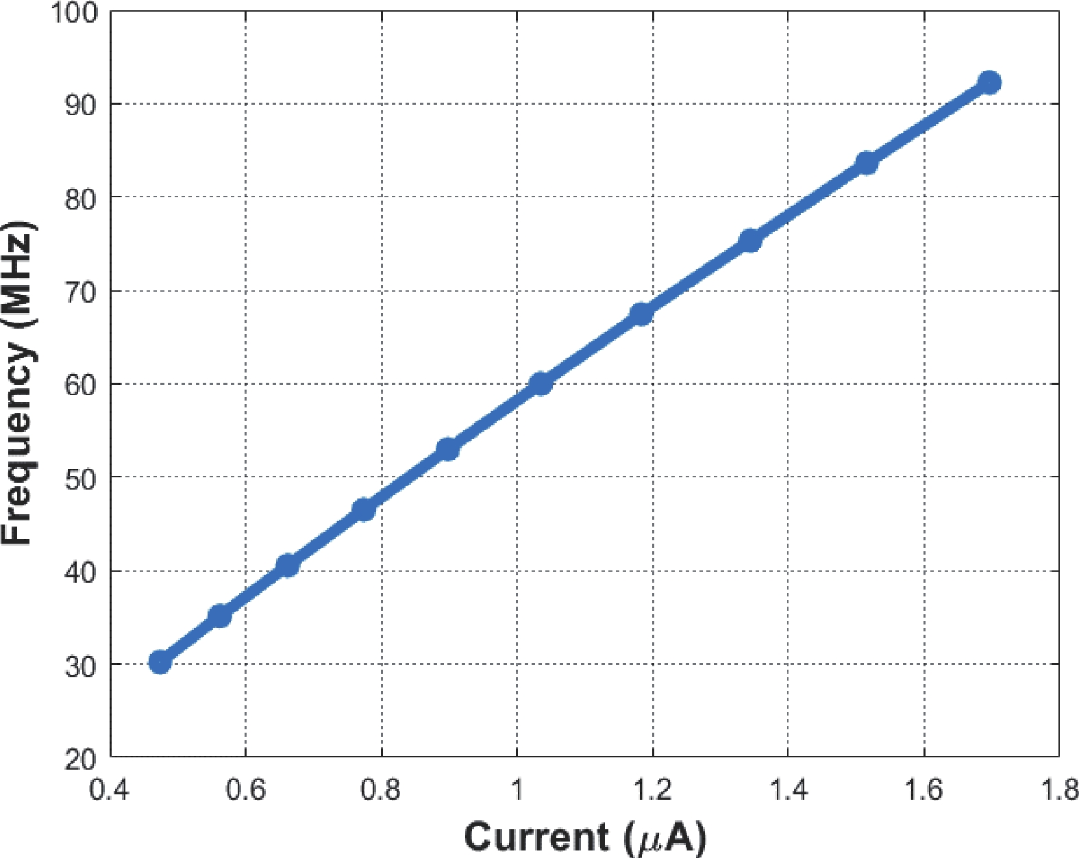
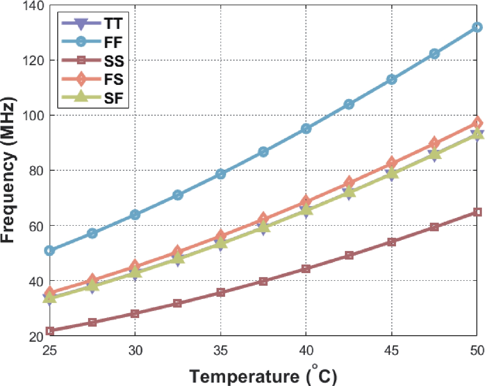
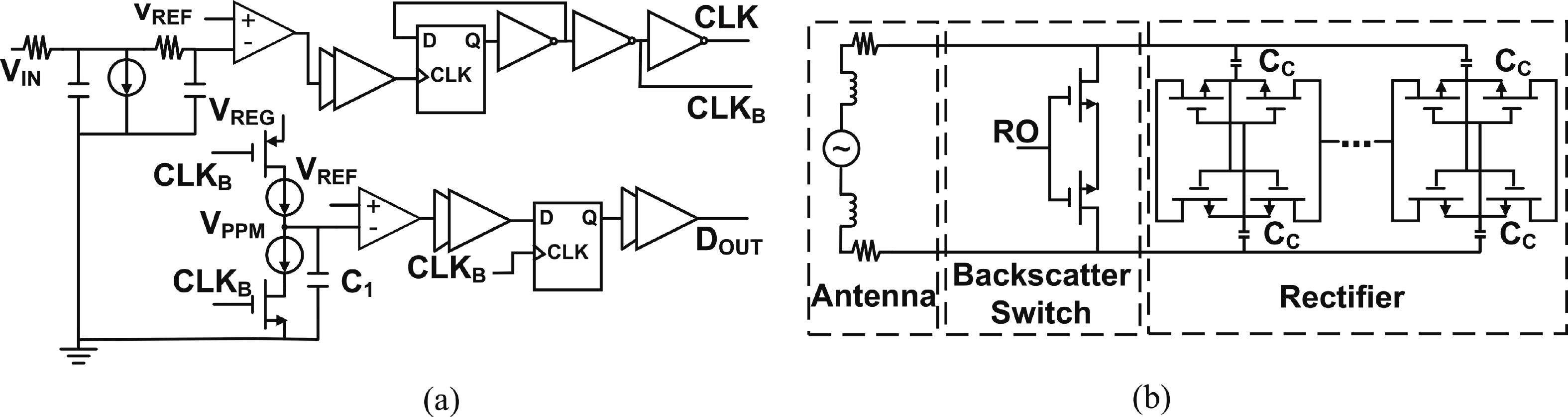
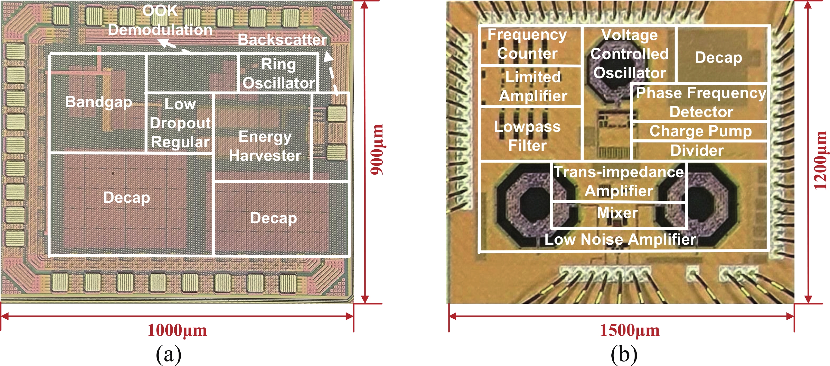
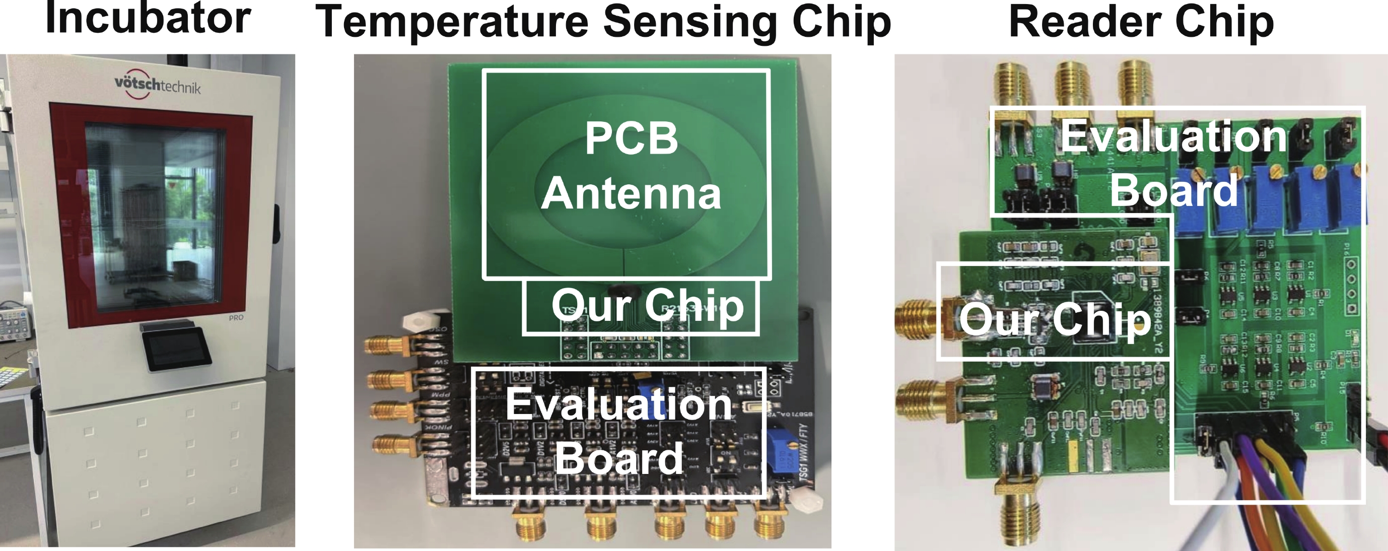
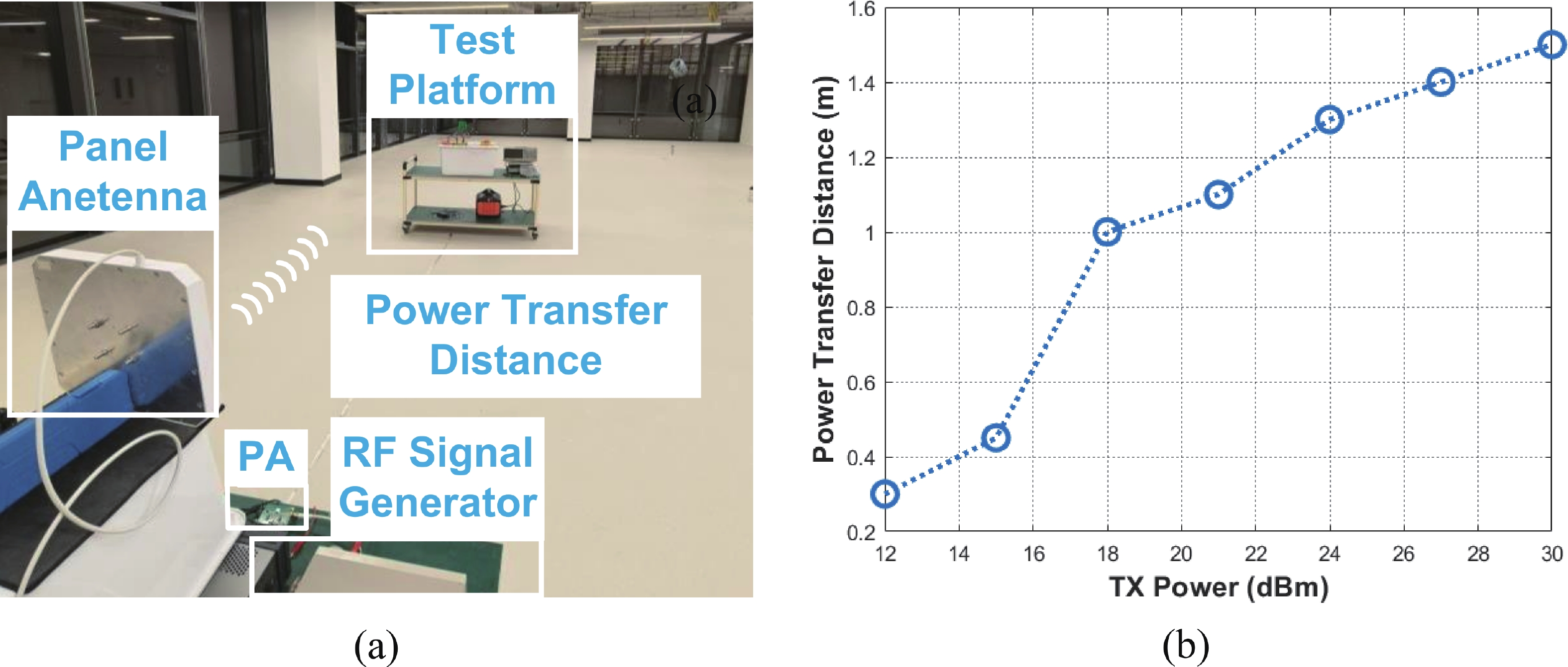
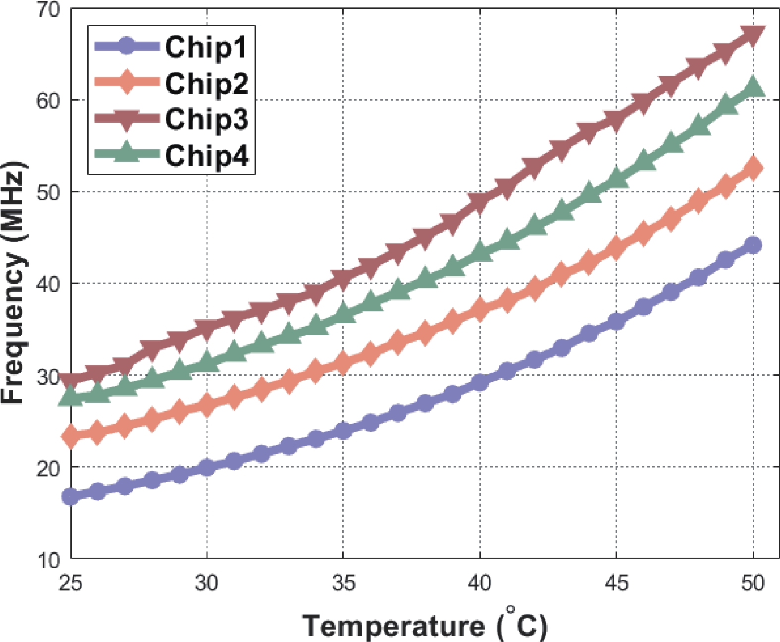
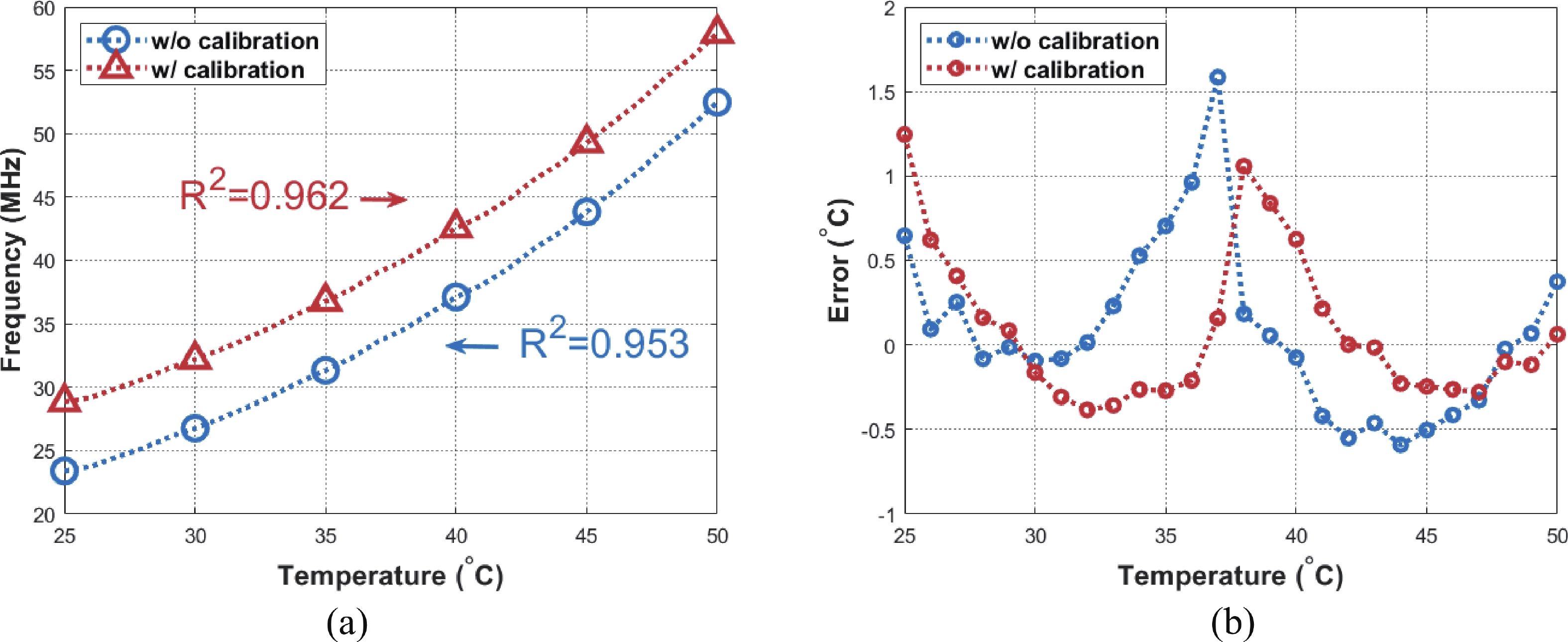
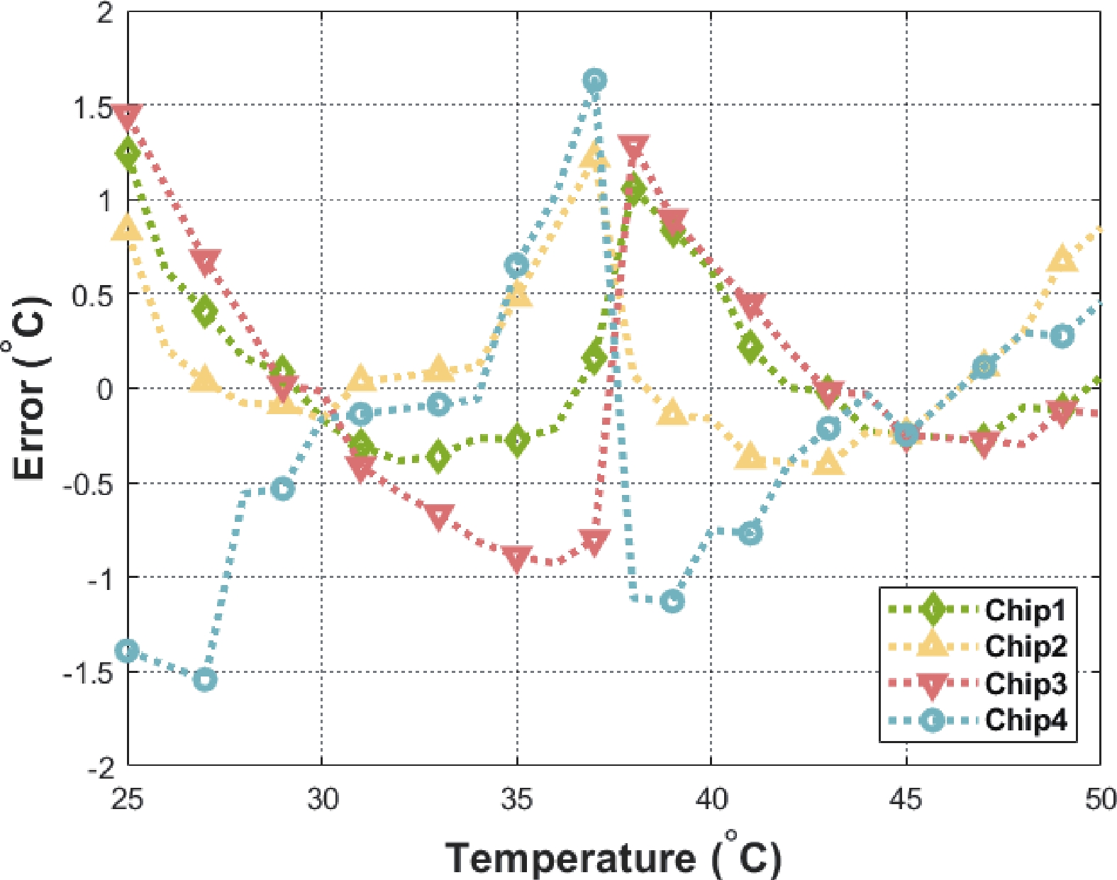
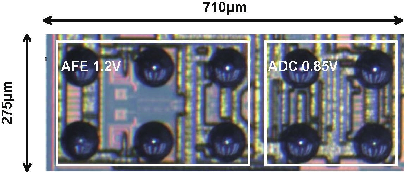
In the applications such as food production, the environmental temperature should be measured continuously during the entire process, which requires an ultra-low-power temperature sensor for long-termly monitoring. Conventional temperature sensors trade the measurement accuracy with power consumption. In this work, we present a battery-free wireless temperature sensing chip for long-termly monitoring during food production. A calibrated oscillator-based CMOS temperature sensor is proposed instead of the ADC-based power-hungry circuits in conventional works. In addition, the sensor chip can harvest the power transferred by a remote reader to eliminate the use of battery. Meanwhile, the system conducts wireless bidirectional communication between the sensor chip and reader. In this way, the temperature sensor can realize both a high precision and battery-free operation. The temperature sensing chip is fabricated in 55 nm CMOS process, and the reader chip is implemented in 65 nm CMOS technology. Experimental results show that the temperature measurement error achieves ±1.6 °C from 25 to 50 °C, with battery-free readout by a remote reader.

J. Semicond.
2025, 46(6): 062203 doi: 10.1088/1674-4926/24120045
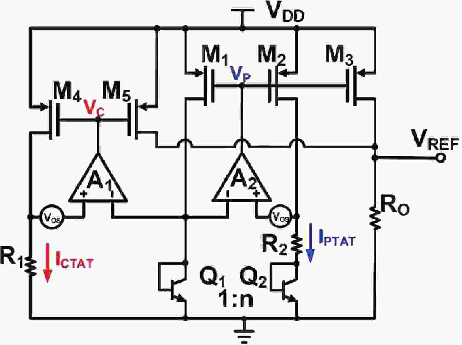
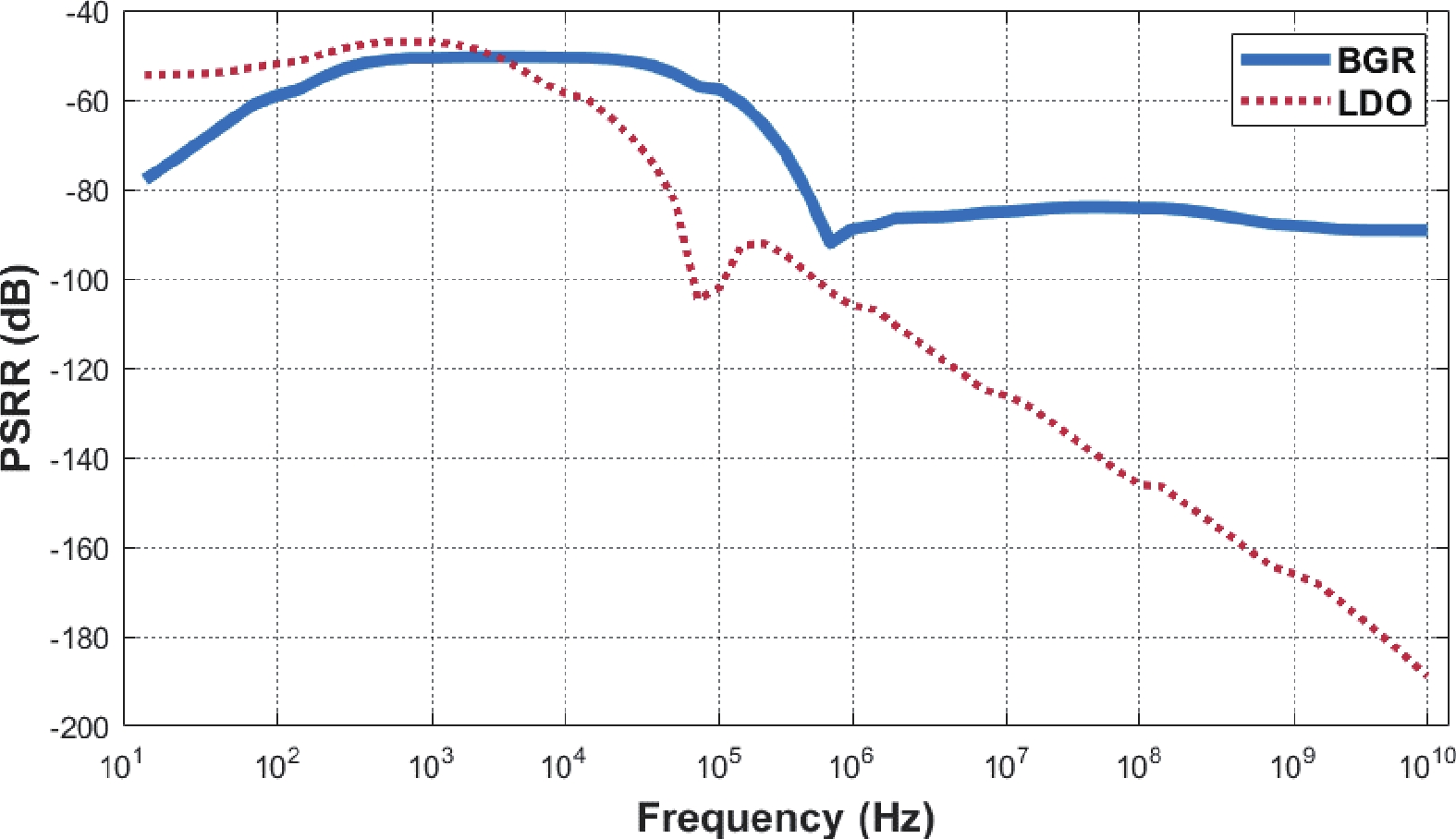
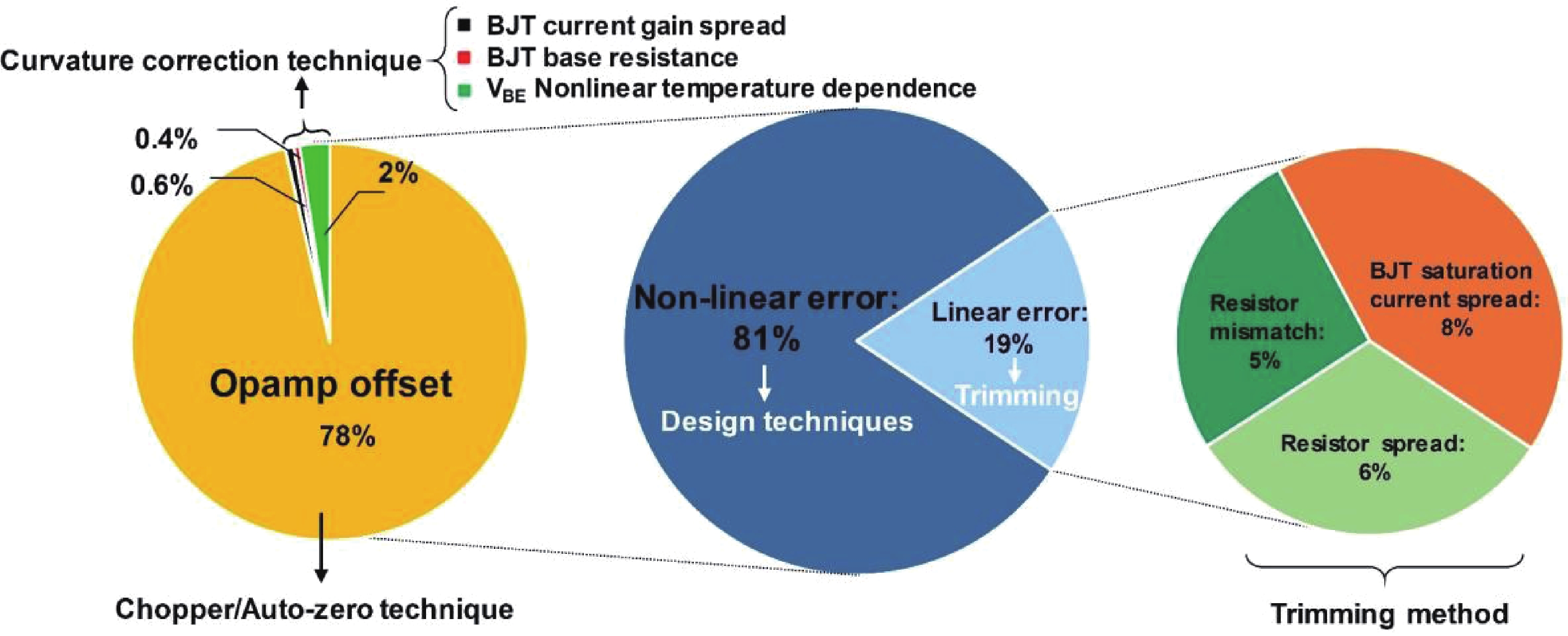
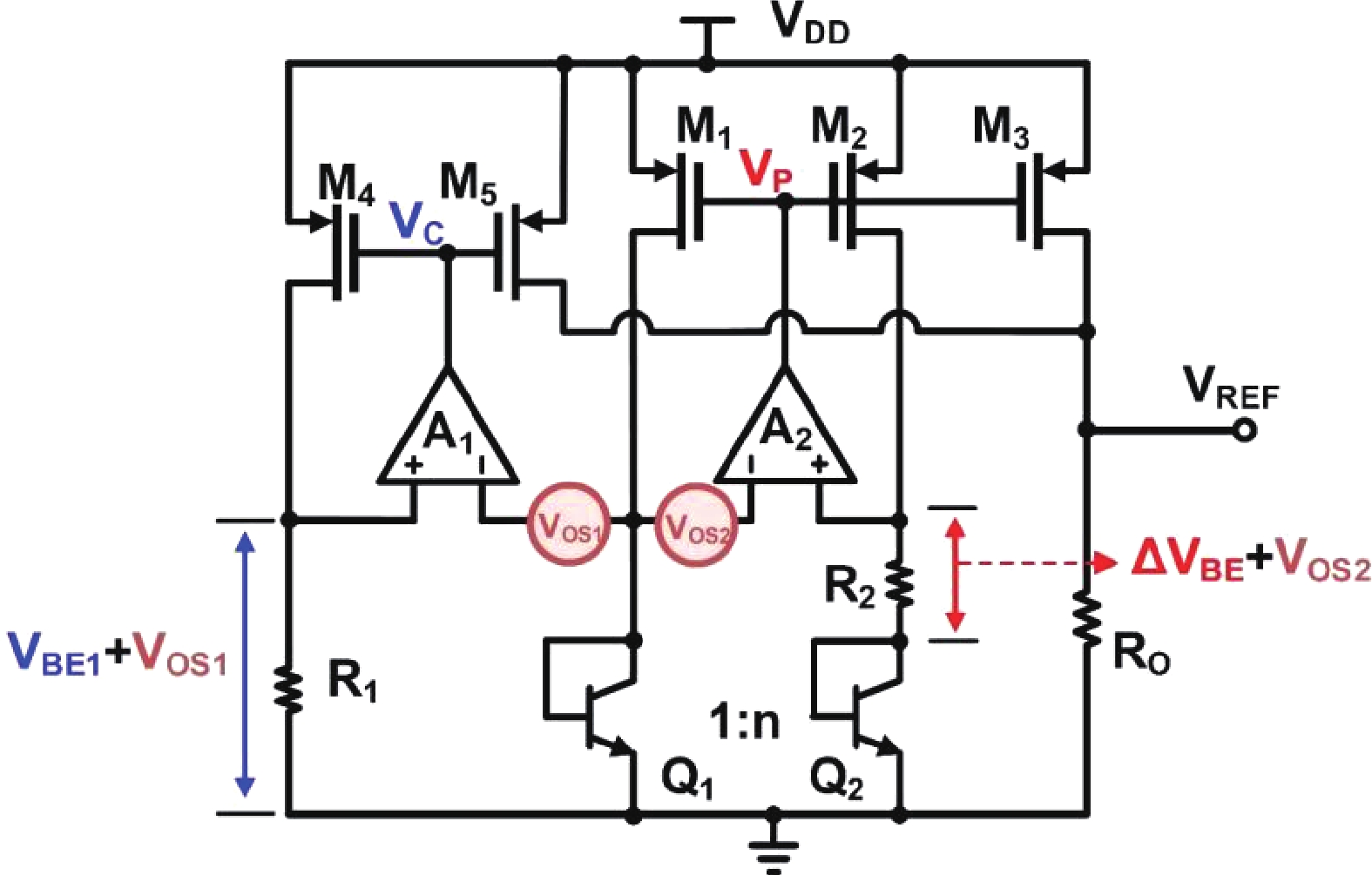
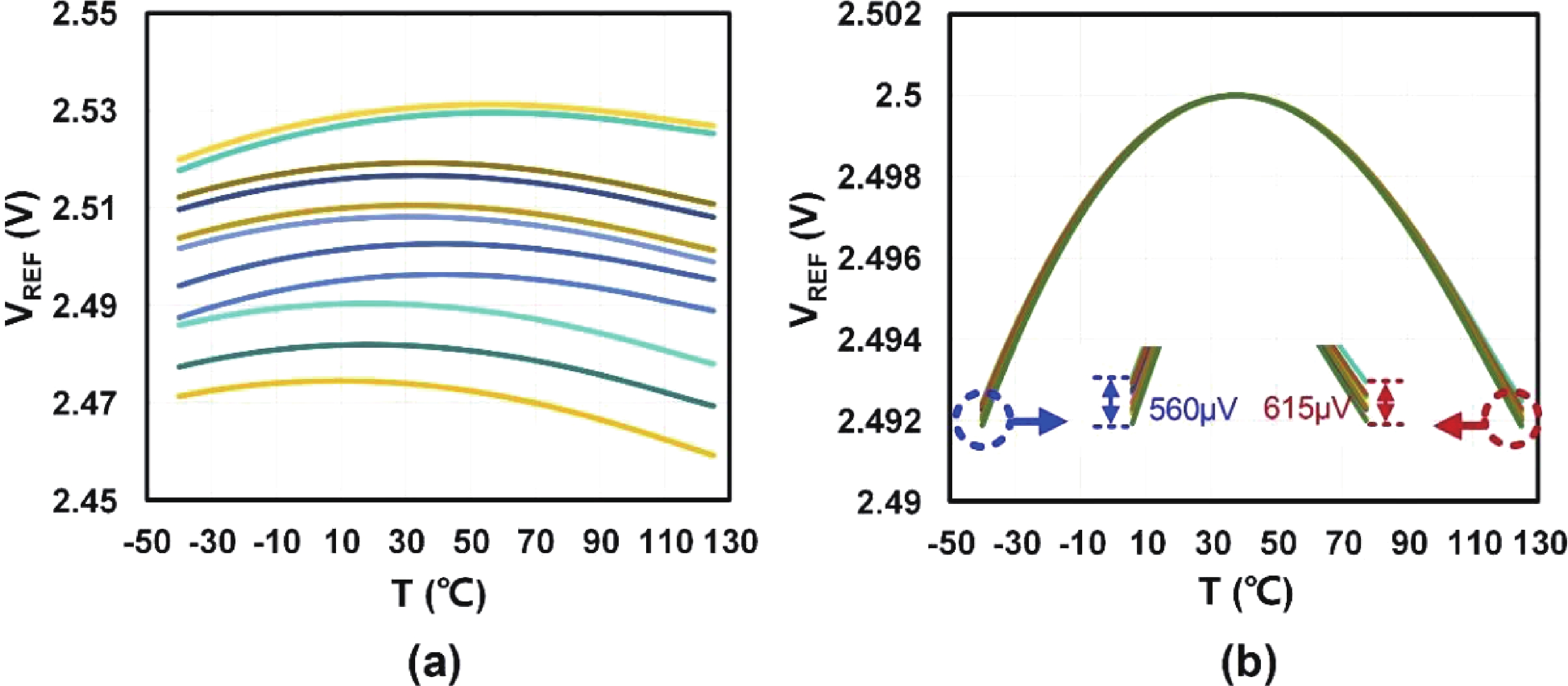
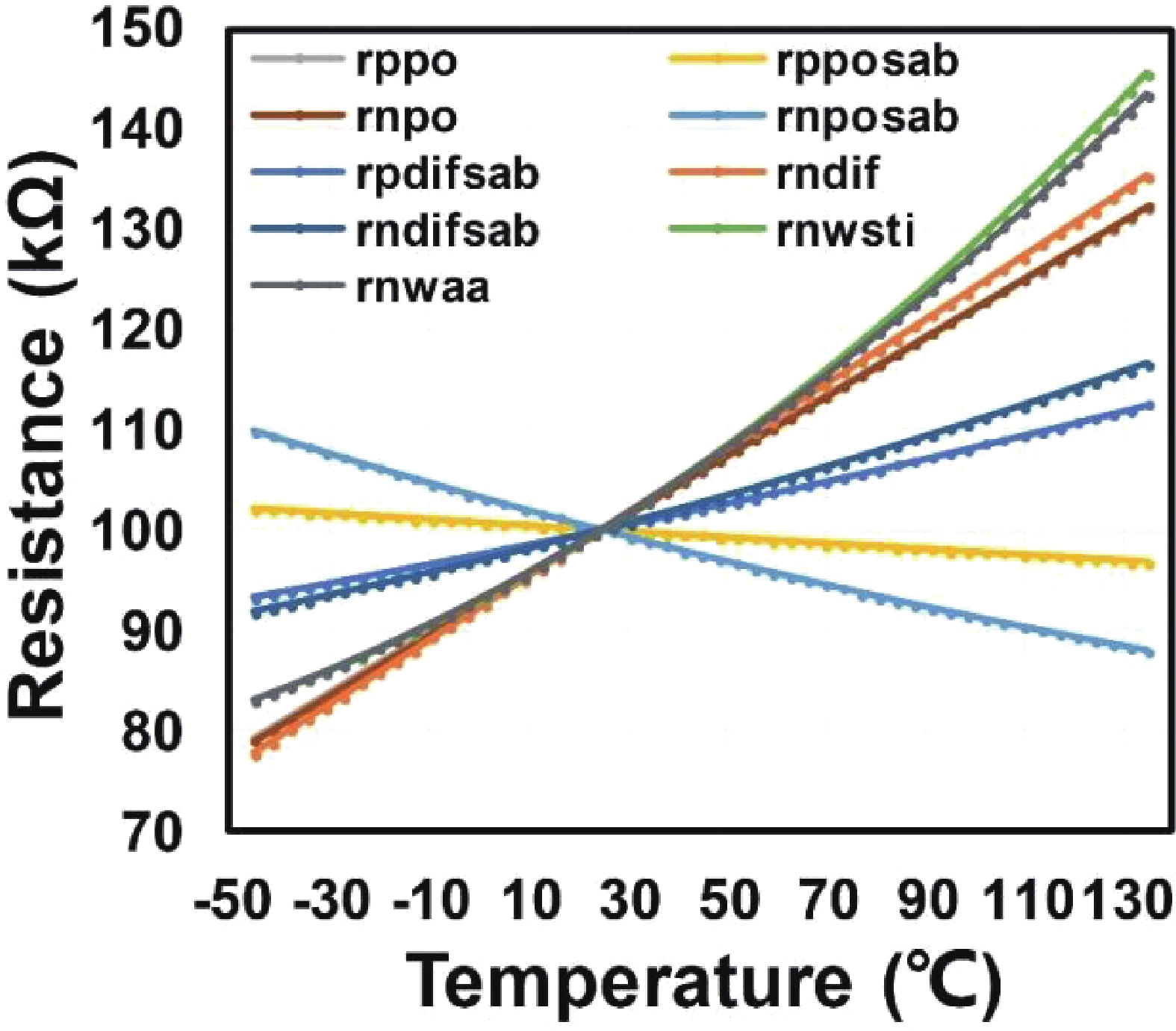
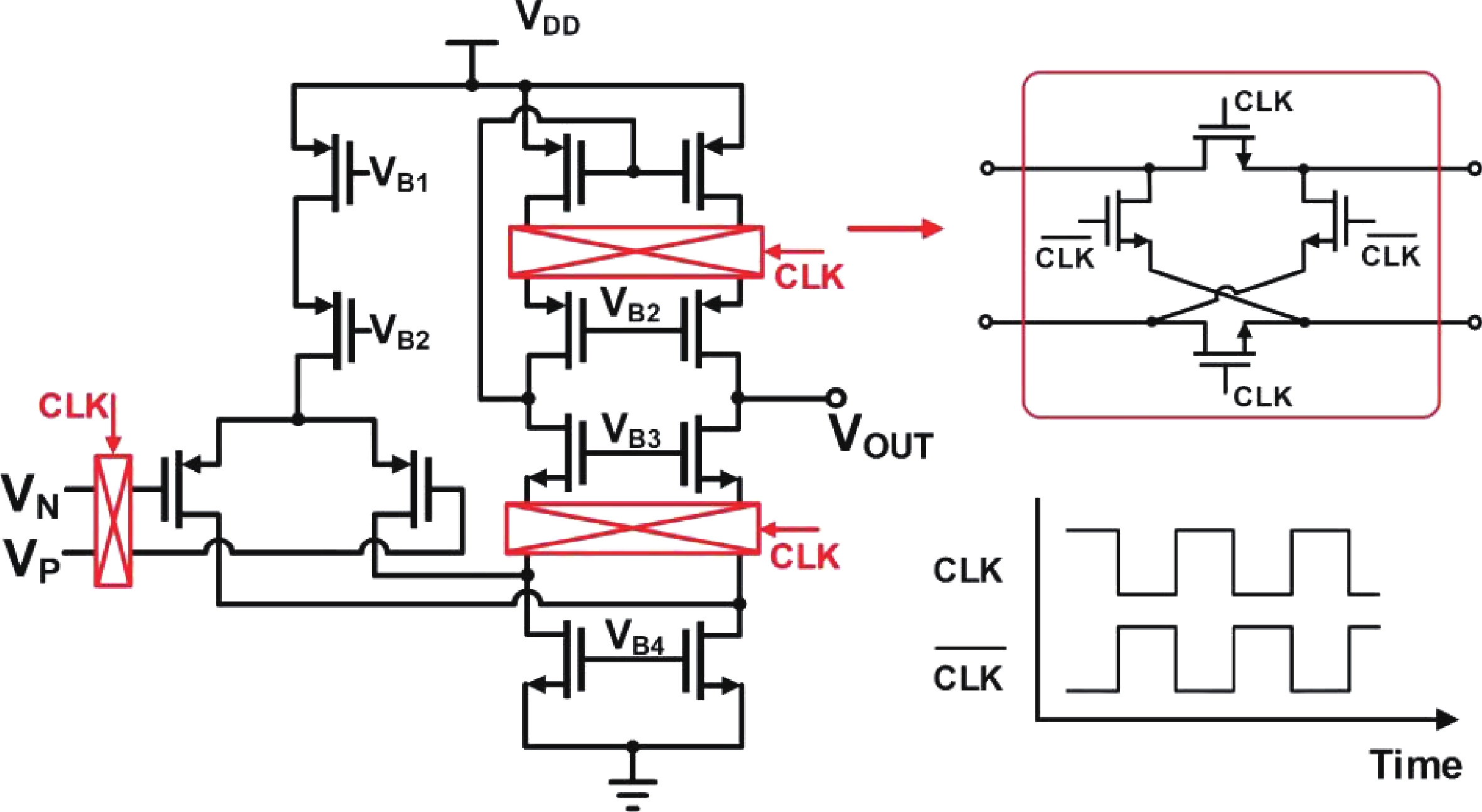
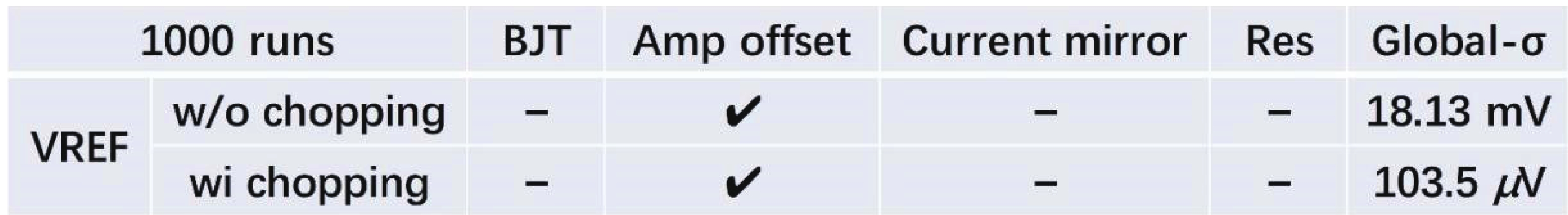
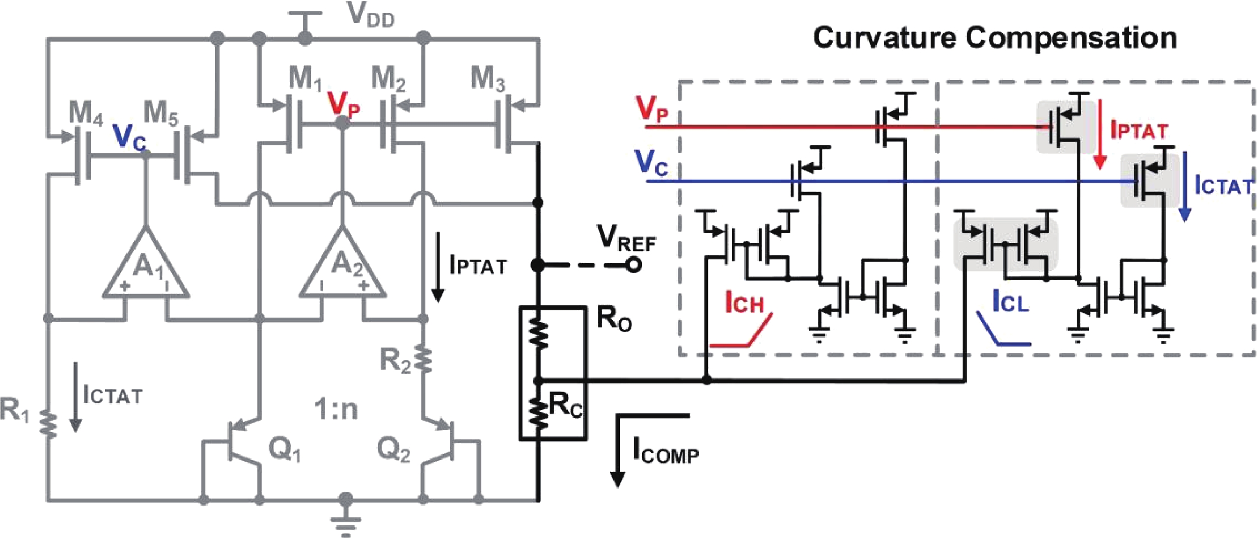
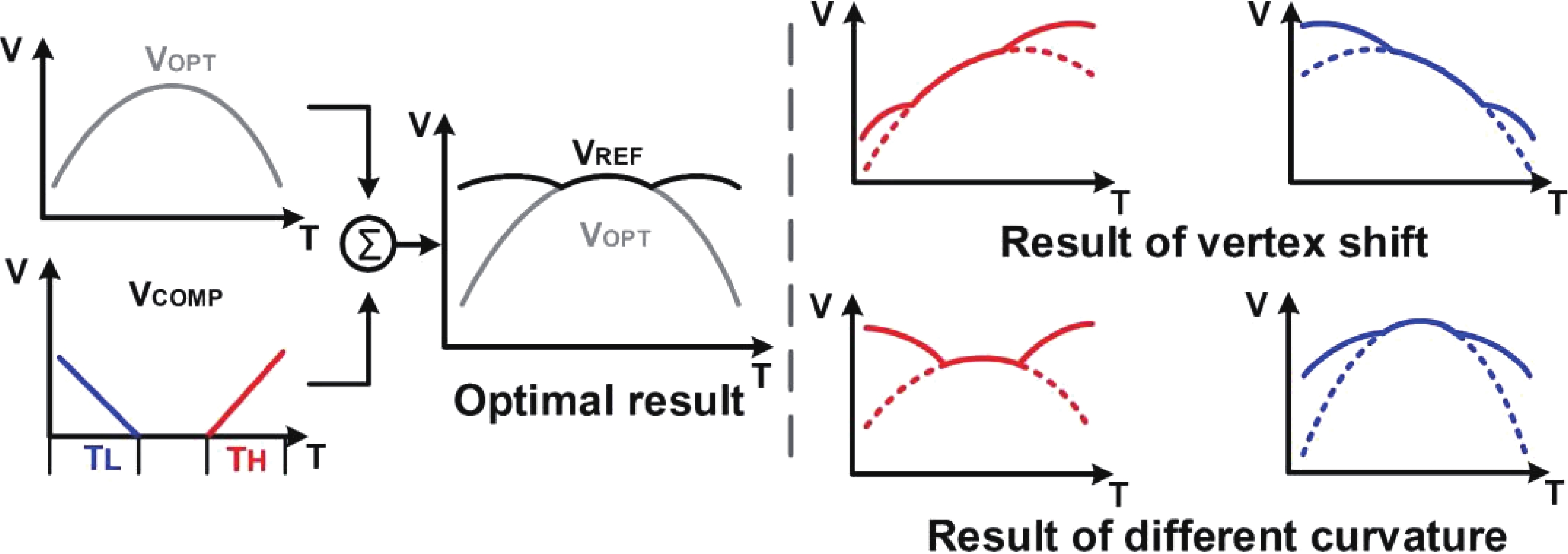
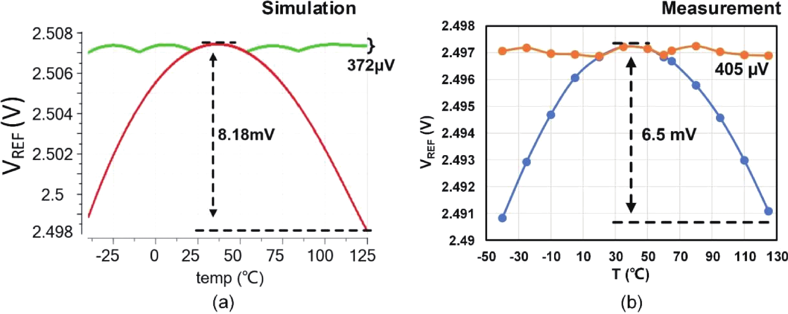
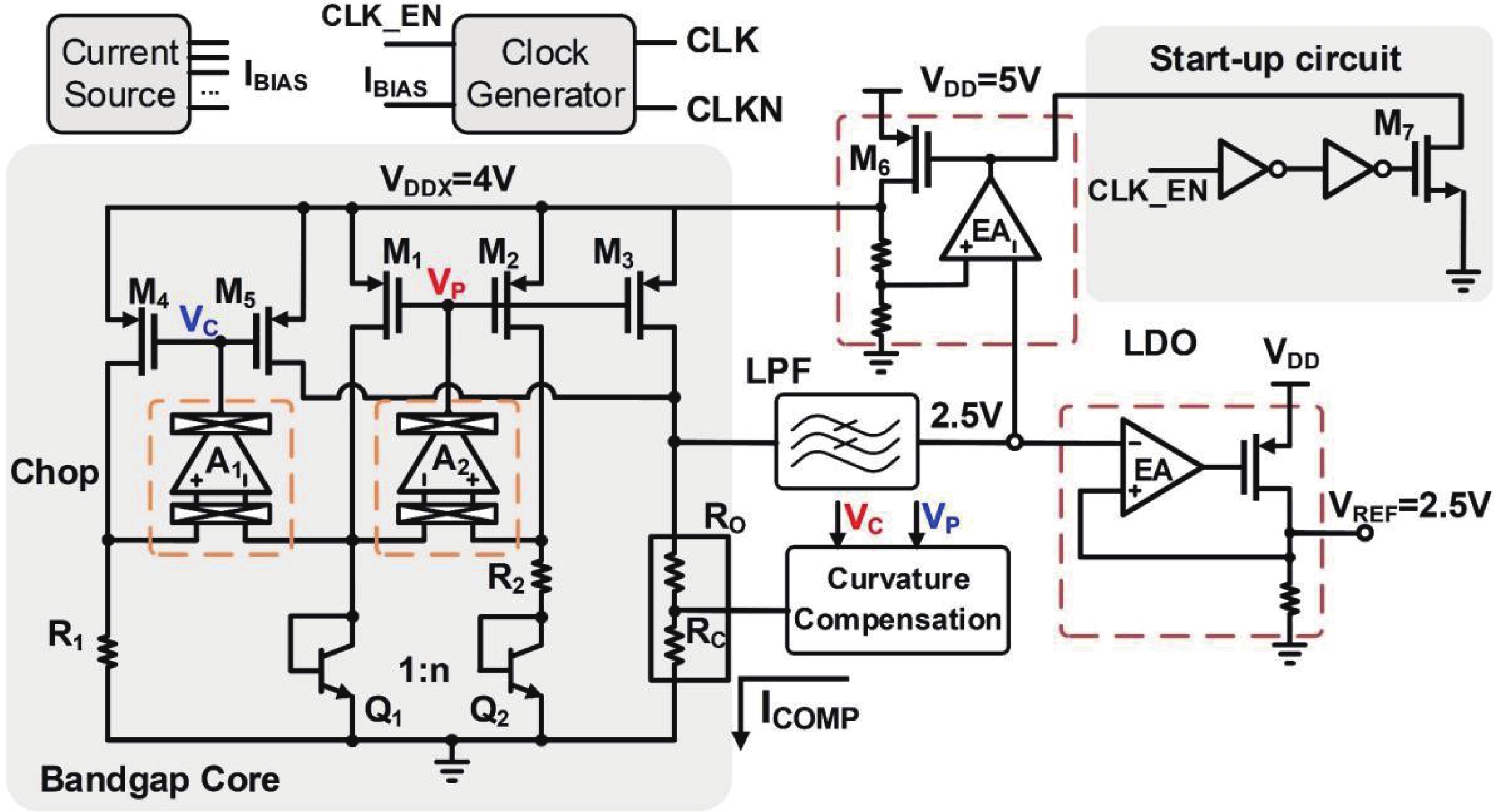
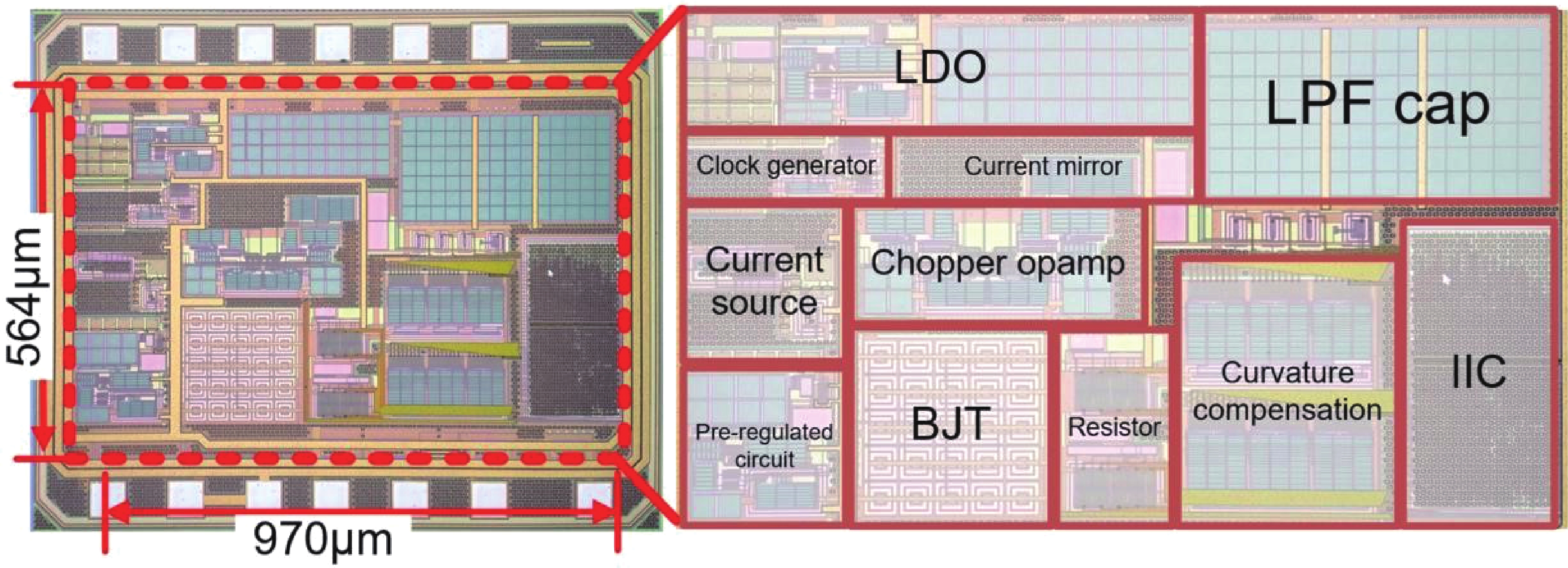
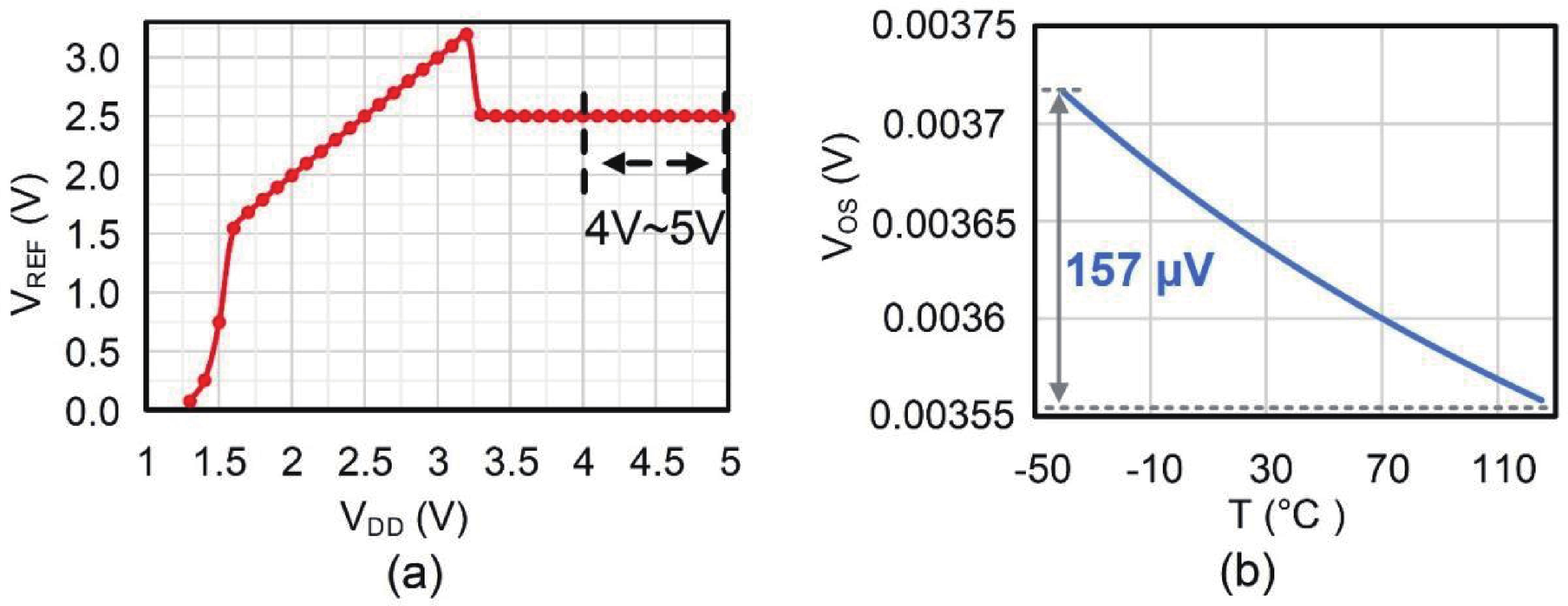
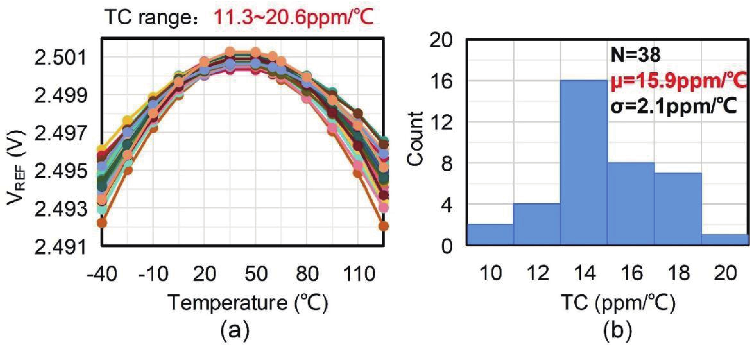
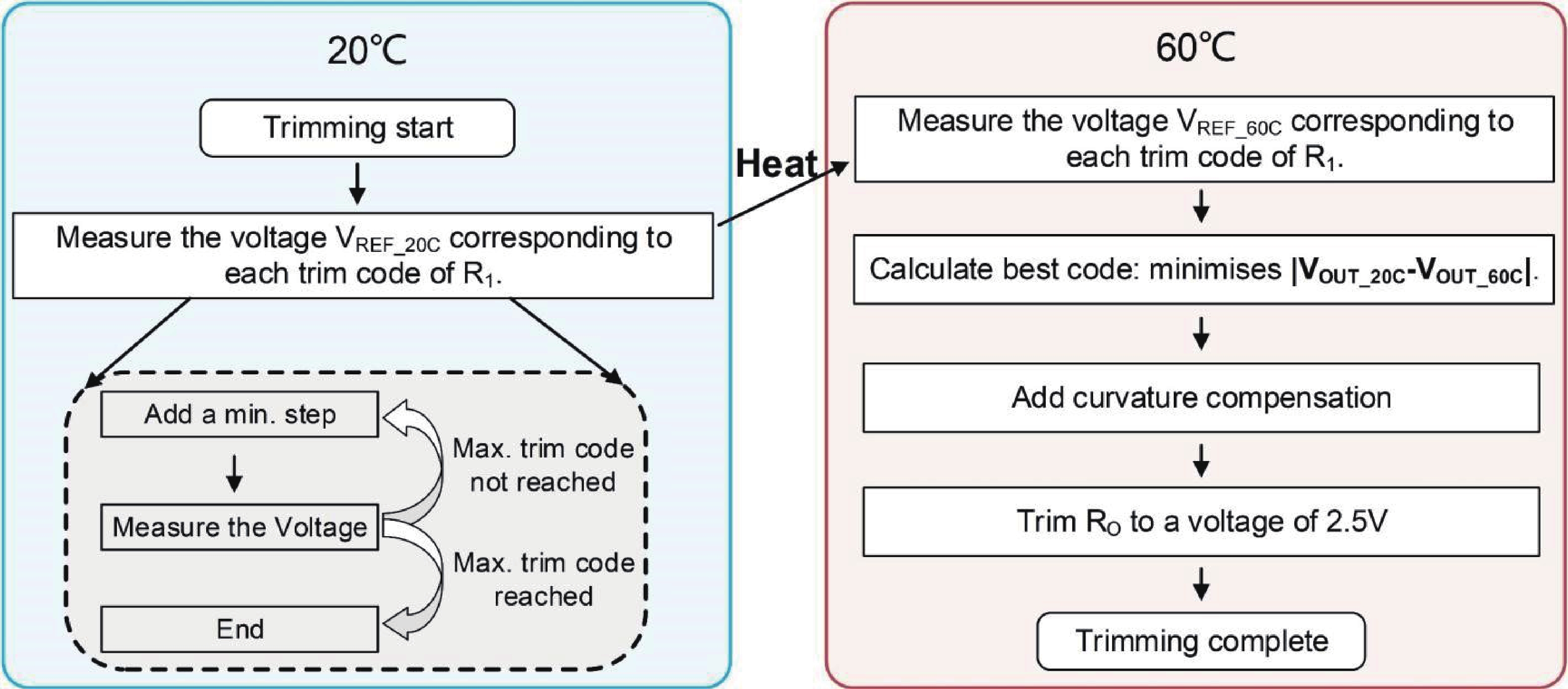
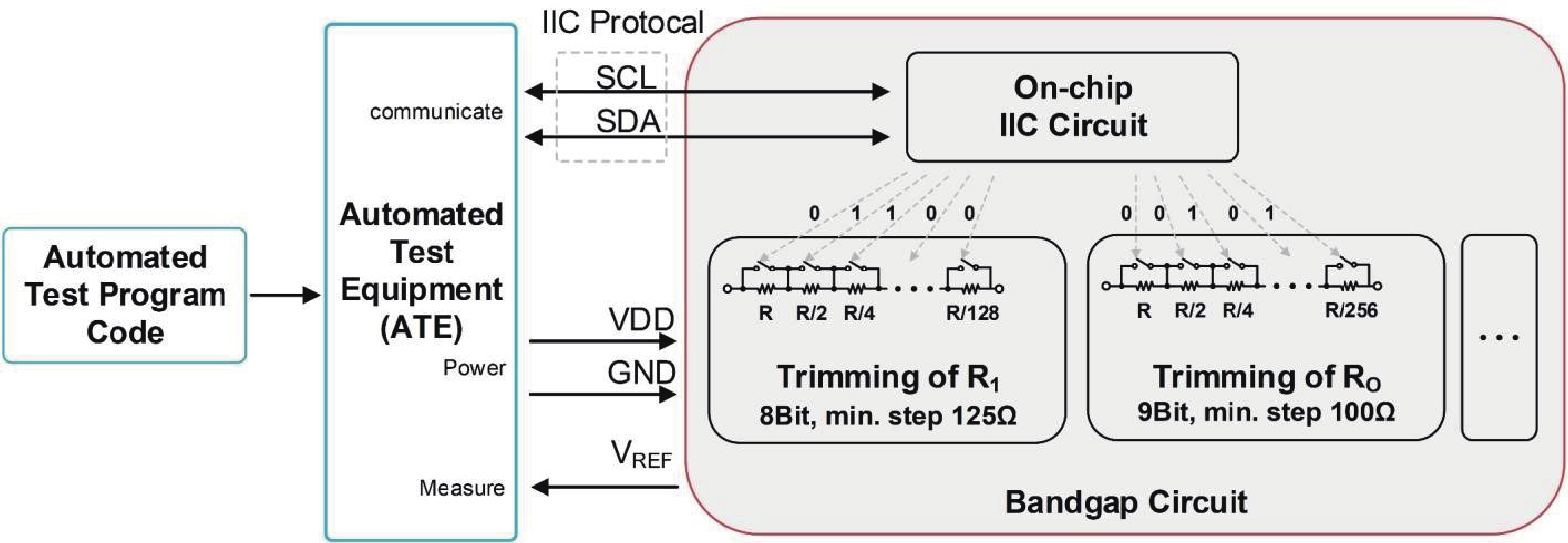
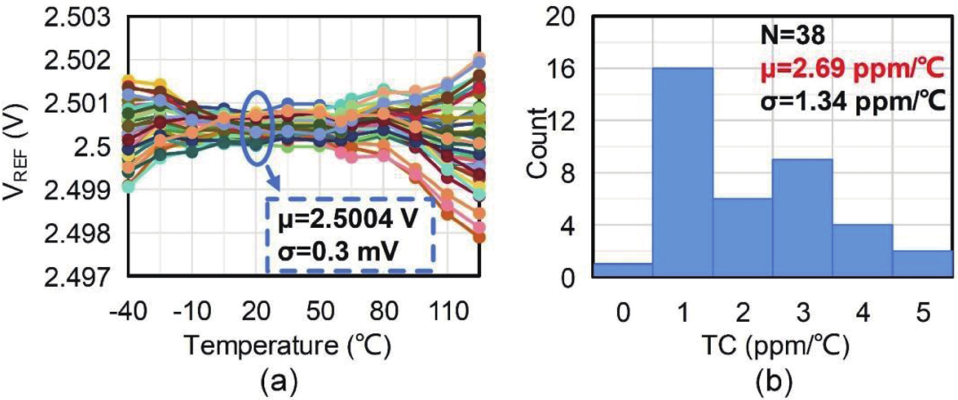
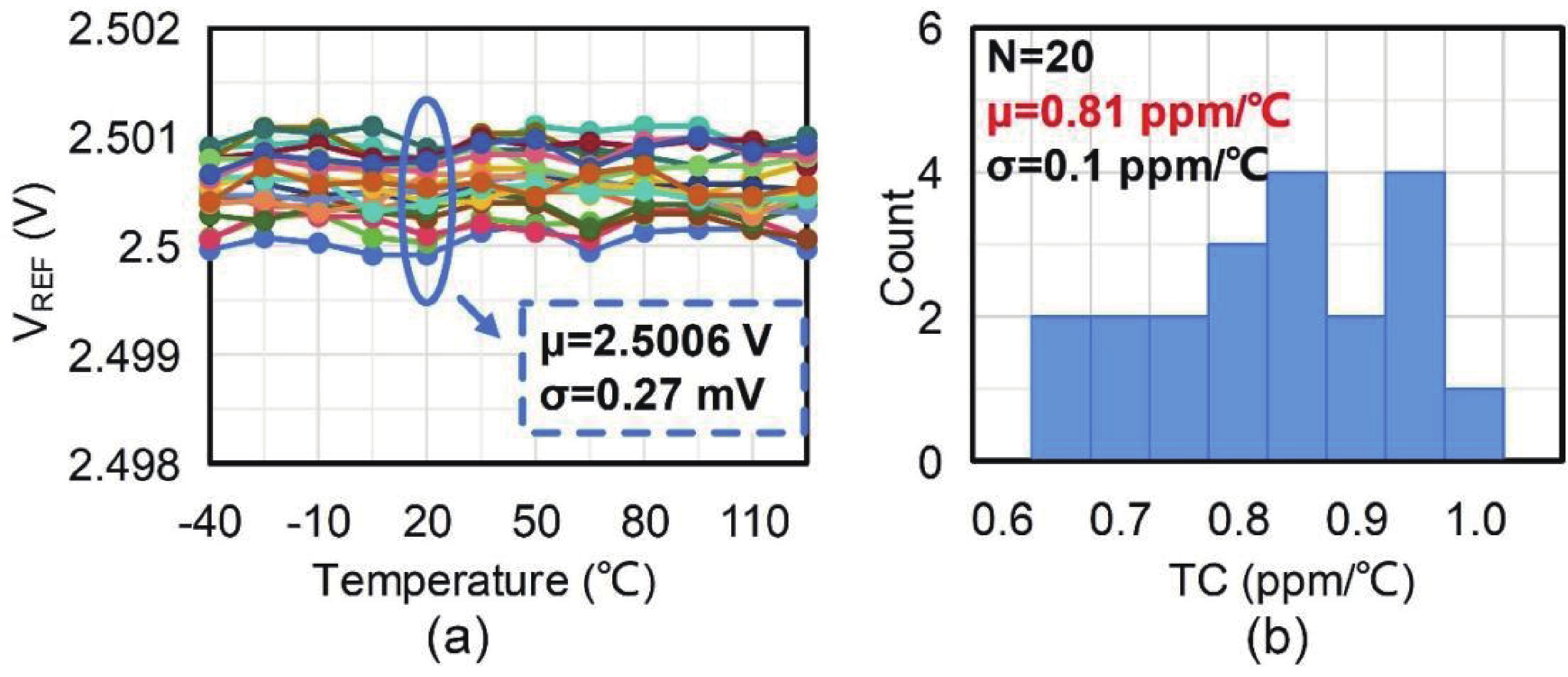
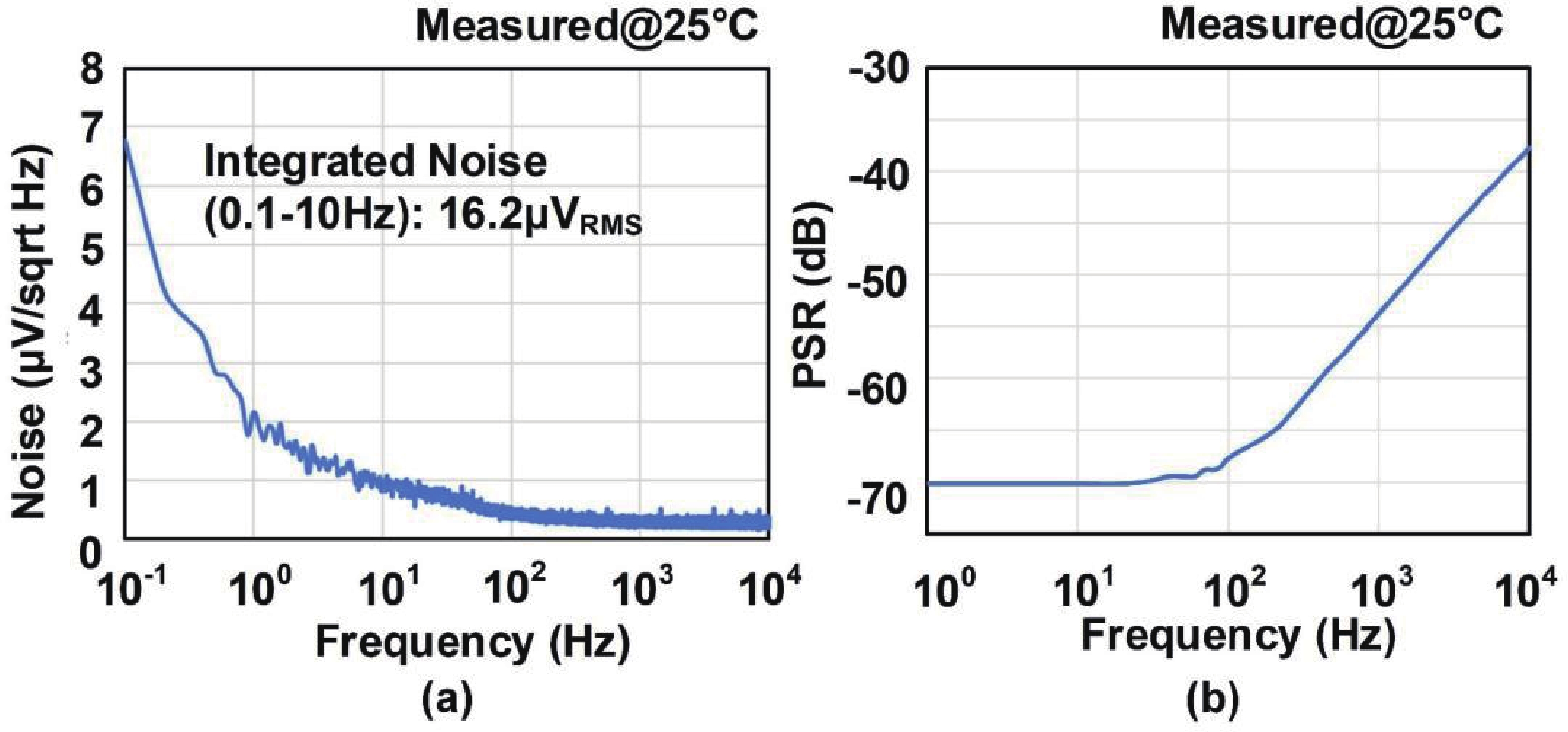
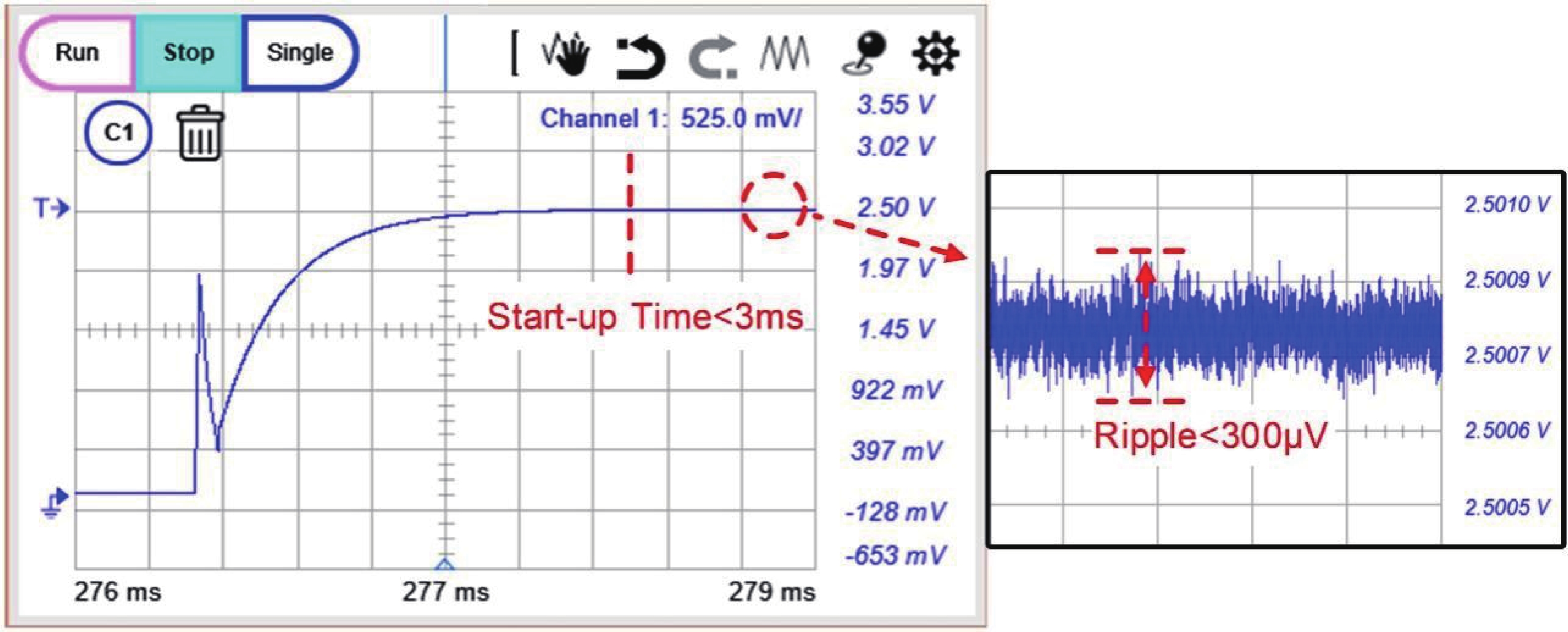
This paper introduces a high-precision bandgap reference (BGR) designed for battery management systems (BMS), featuring an ultra-low temperature coefficient (TC) and line sensitivity (LS). The BGR employs a current-mode scheme with chopped op-amps and internal clock generators to eliminate op-amp offset. A low dropout regulator (LDO) and a pre-regulator enhance output driving and LS, respectively. Curvature compensation enhances the TC by addressing higher-order nonlinearity. These approaches, effective near room temperature, employs trimming at both 20 and 60 °C. When combined with fixed curvature correction currents, it achieves an ultra-low TC for each chip. Implemented in a CMOS 180 nm process, the BGR occupies 0.548 mm² and operates at 2.5 V with 84 μA current draw from a 5 V supply. An average TC of 2.69 ppm/°C with two-point trimming and 0.81 ppm/°C with multi-point trimming are achieved over the temperature range of −40 to 125 °C. It accommodates a load current of 1 mA and an LS of 42 ppm/V, making it suitable for precise BMS applications.
J. Semicond.
2025, 46(6): 062204 doi: 10.1088/1674-4926/25030001
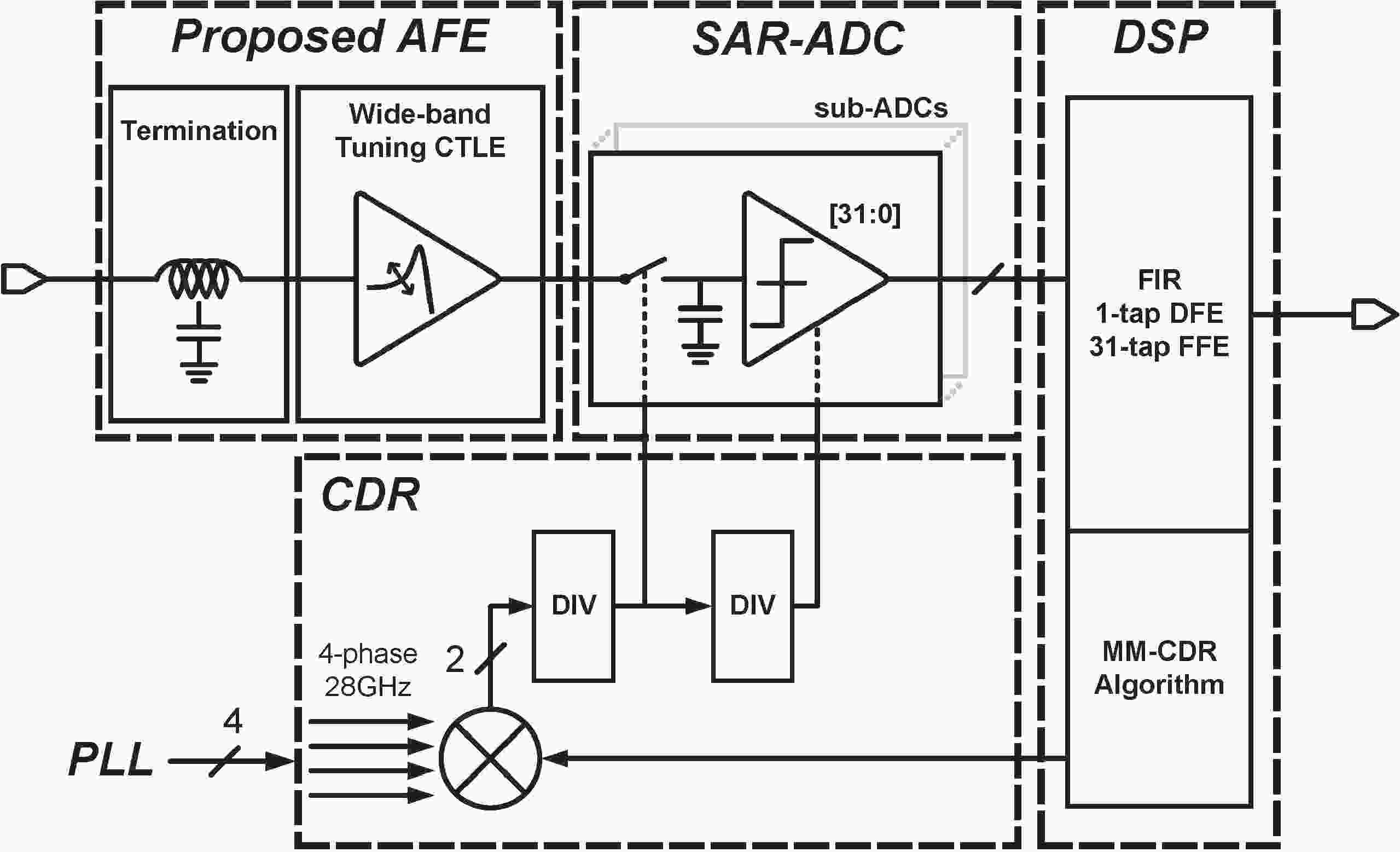
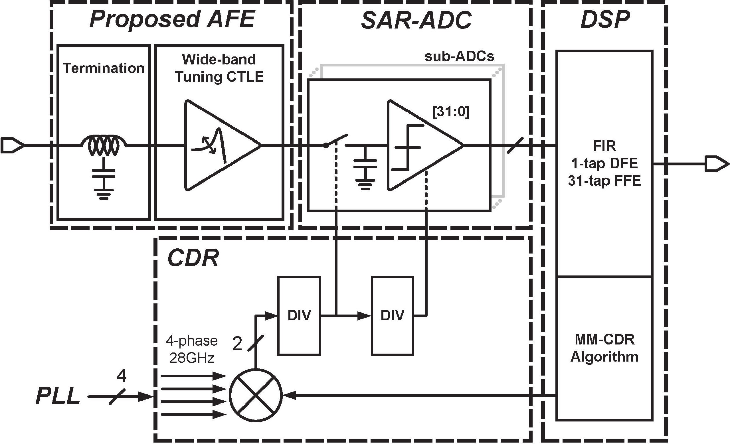
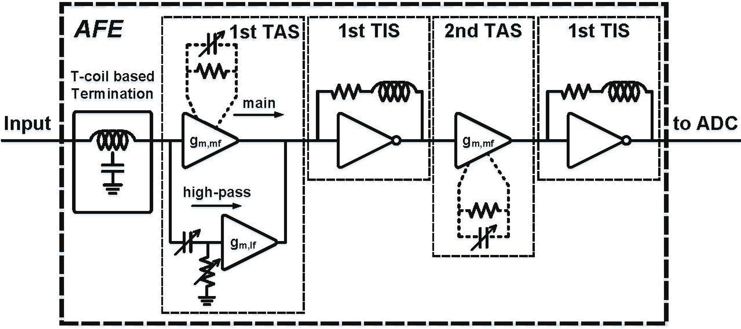
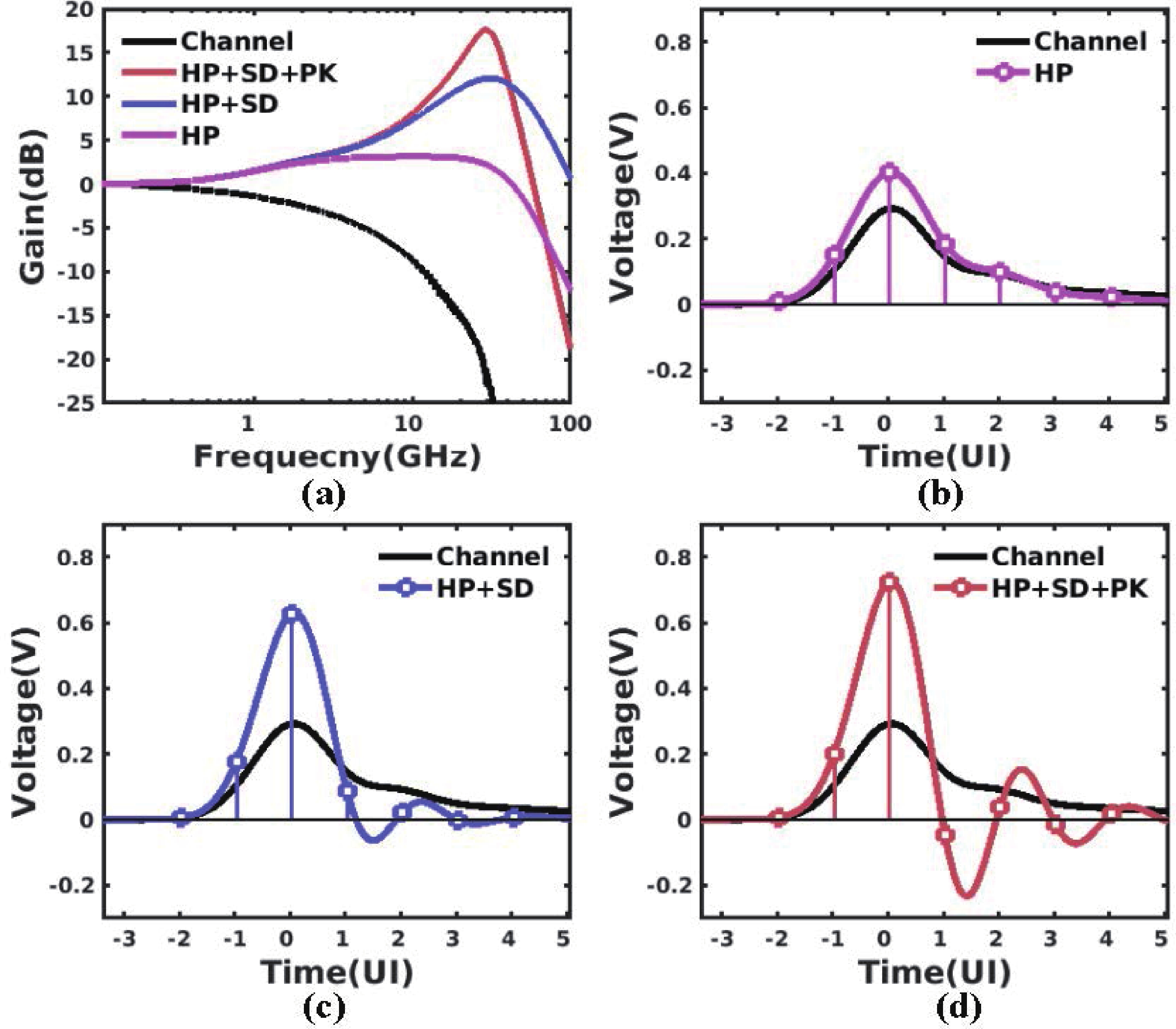
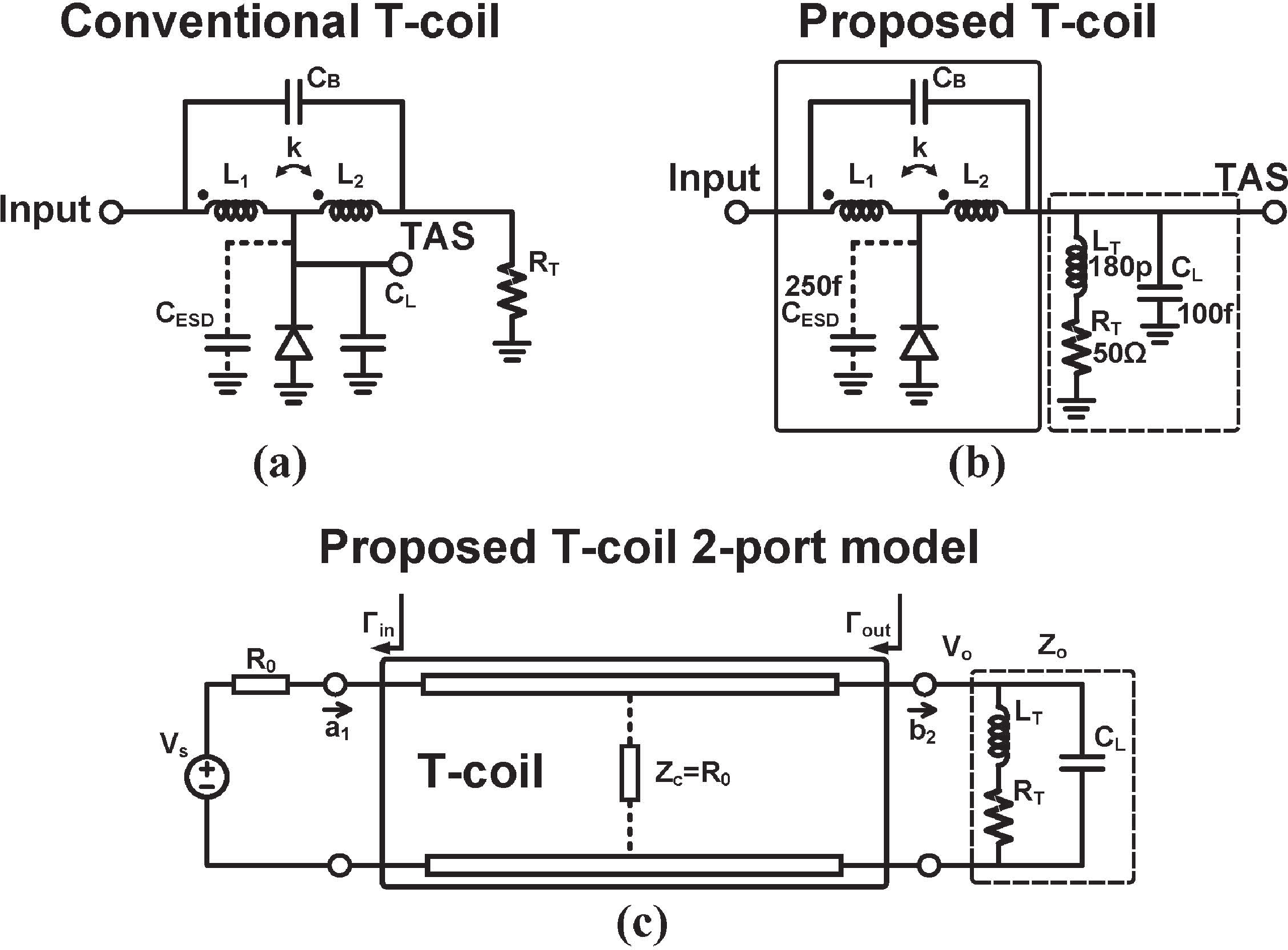
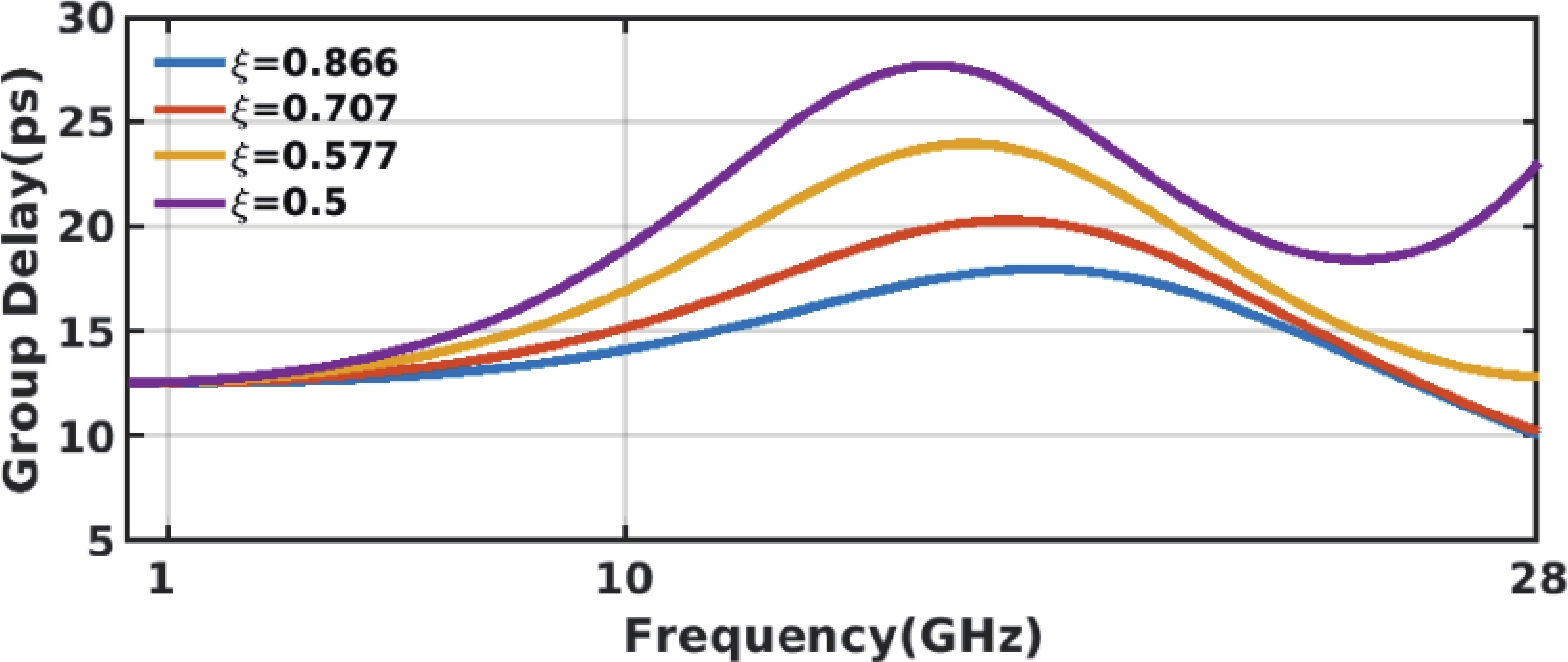
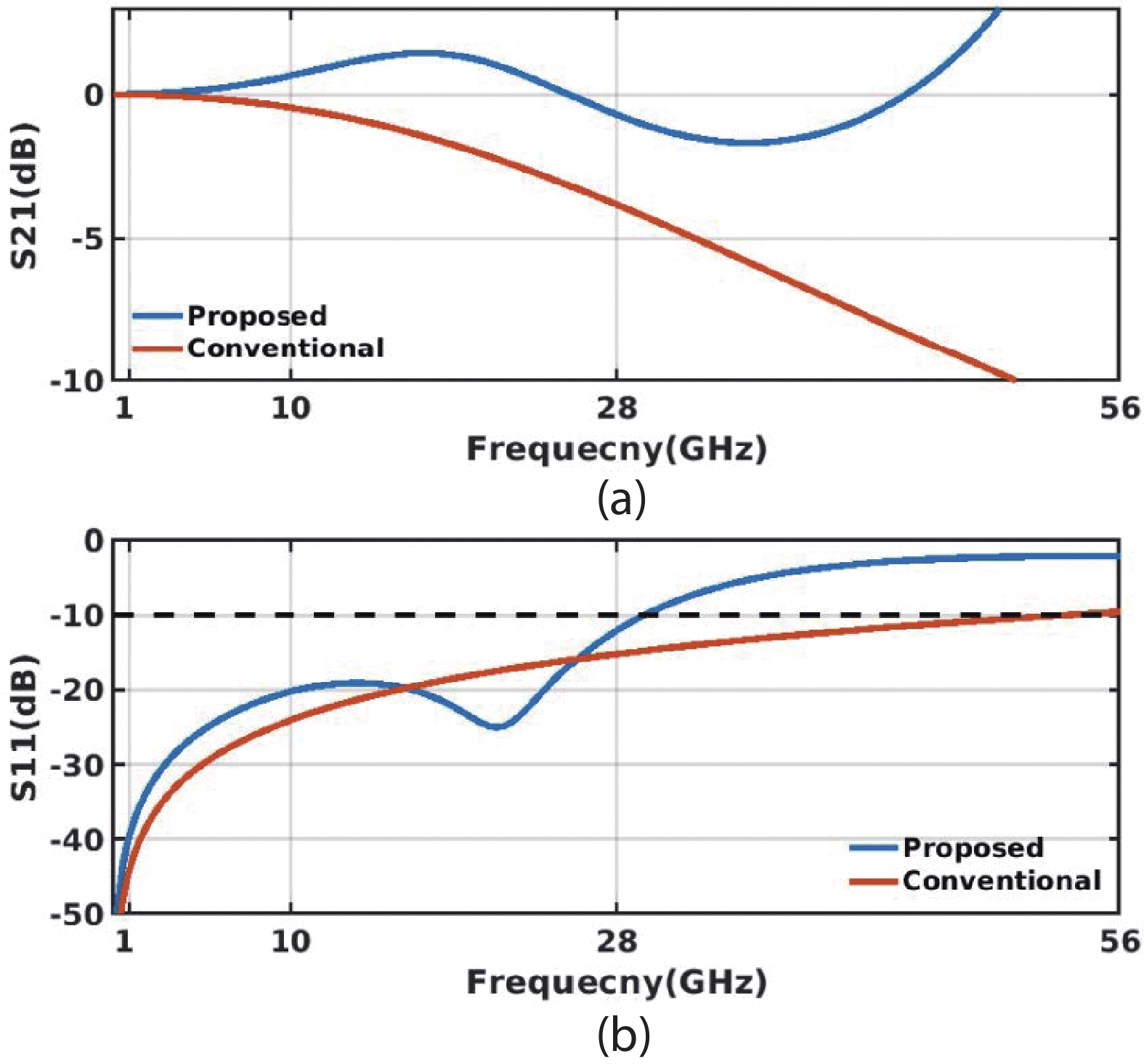
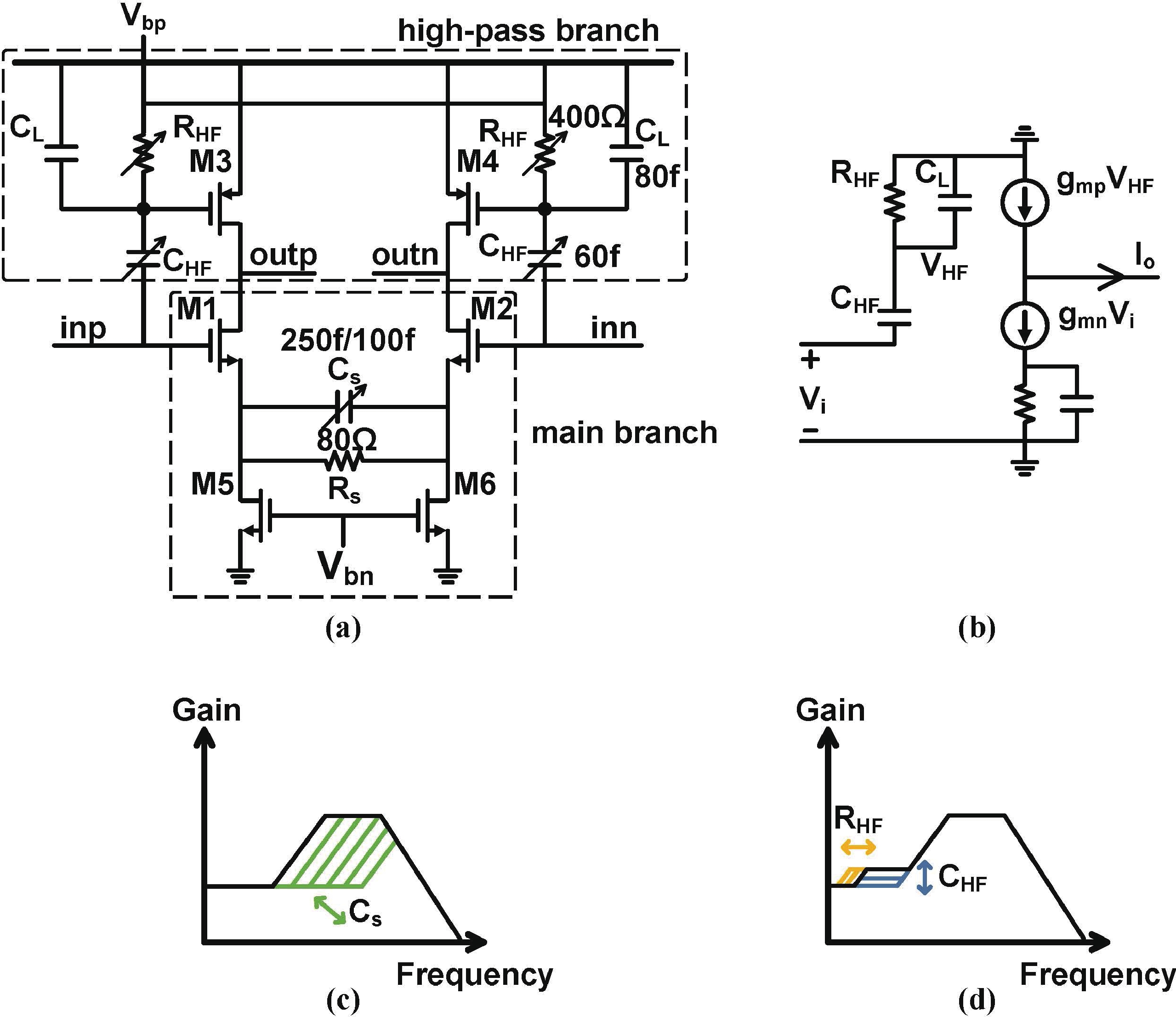
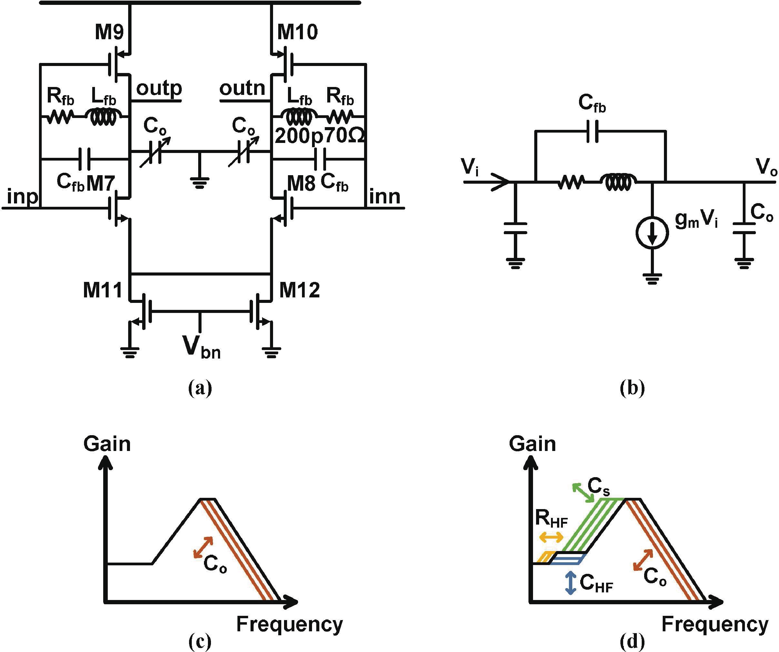
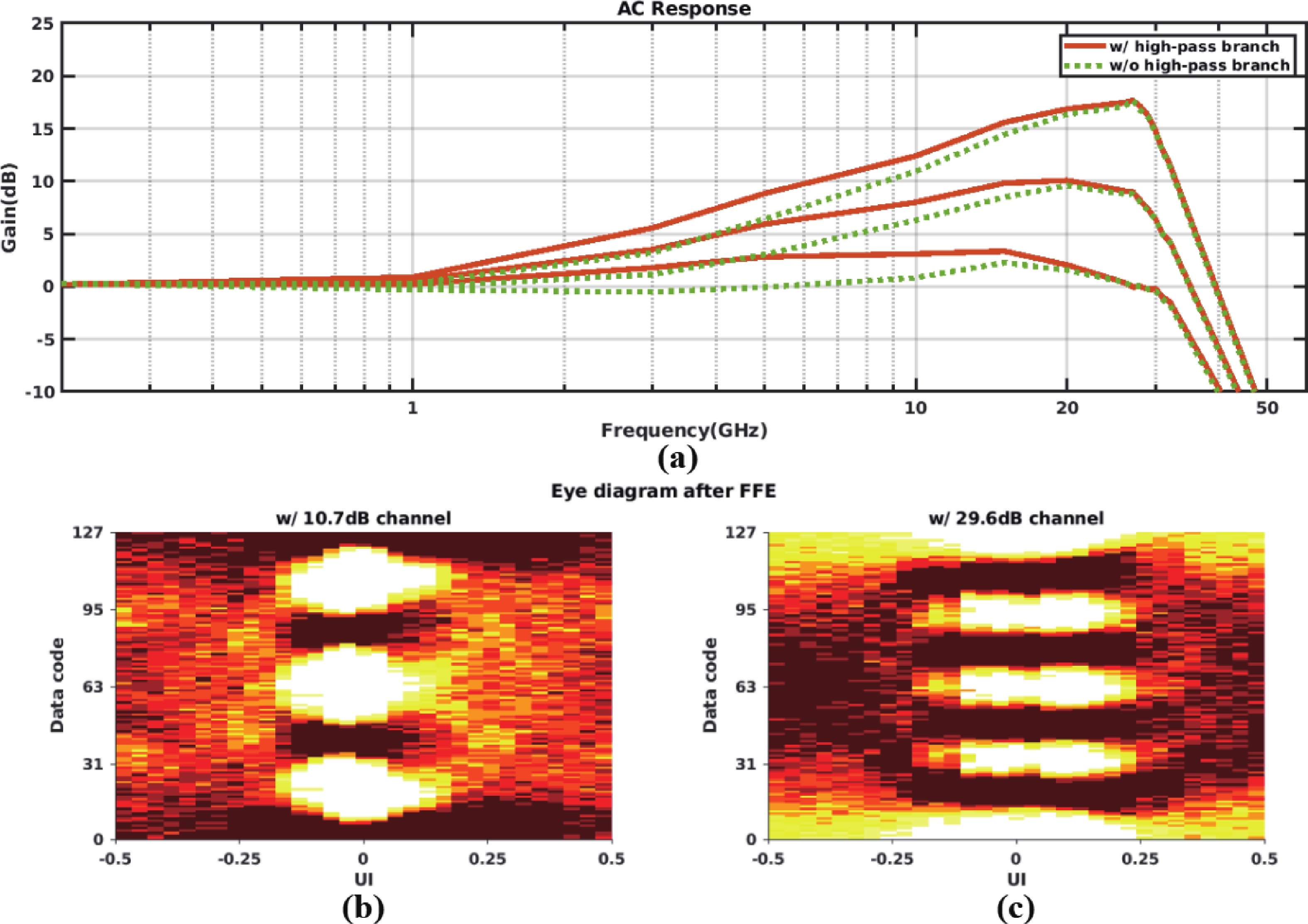
In DSP-based SerDes application, it is essential for AFE to implement a pre-ADC equalization to provide a better signal for ADC and DSP. To meet the various equalization requirements of different channel and transmitter configurations, this paper presents a 112 Gbps DSP-Based PAM4 SerDes receiver with a wide band equalization tuning AFE. The AFE is realized by implementing source degeneration transconductance, feedforward high-pass branch and inductive feedback peaking TIA. The AFE offers a flexible equalization gain tuning of up to 17.5 dB at Nyquist frequency without affecting the DC gain. With the proposed AFE, the receiver demonstrates eye opening after digital FIR equalization and achieves 6 × 10⁻⁹ BER with a 29.6 dB insertion loss channel.
J. Semicond.
2025, 46(6): 061301 doi: 10.1088/1674-4926/24110006

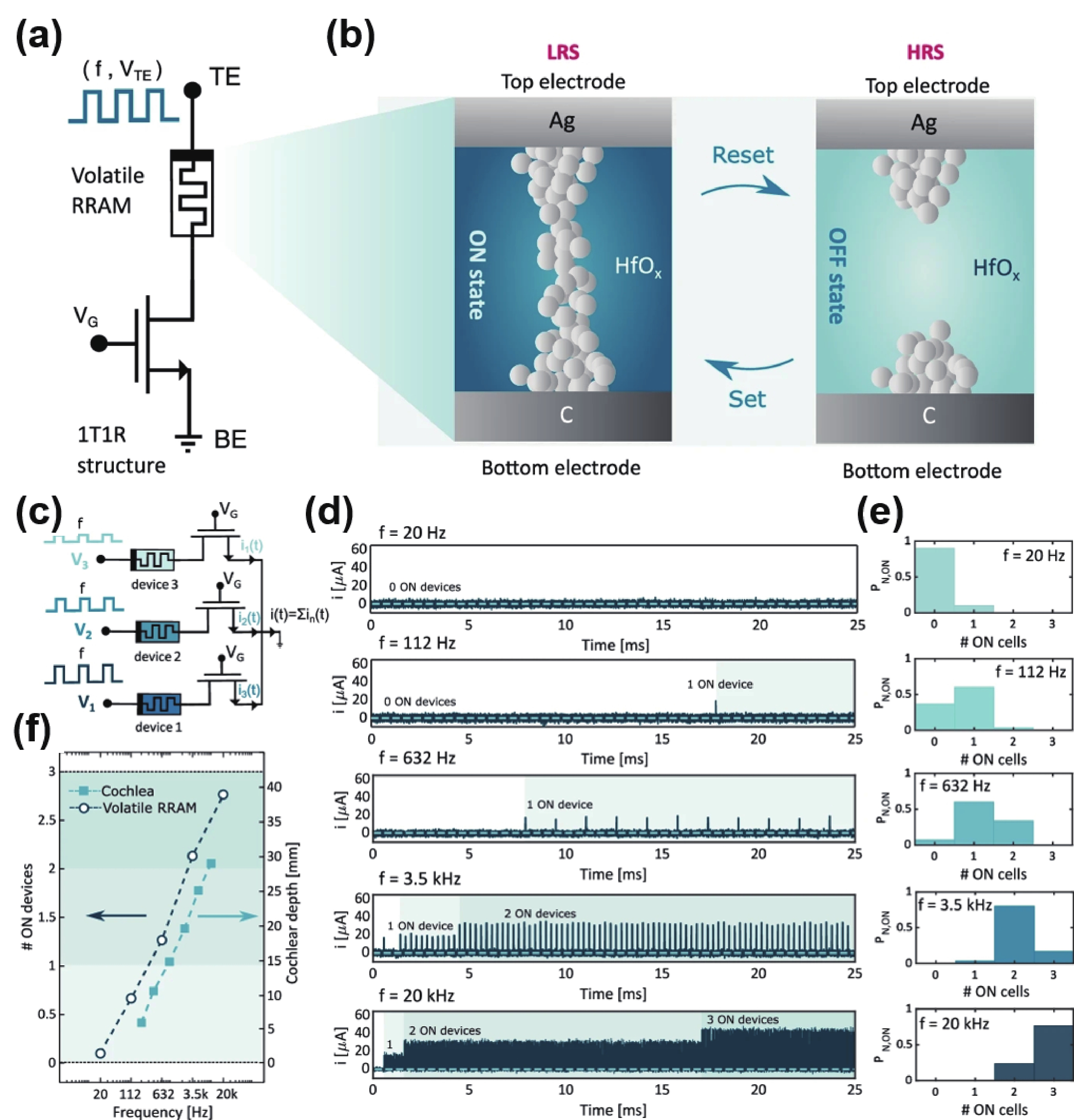
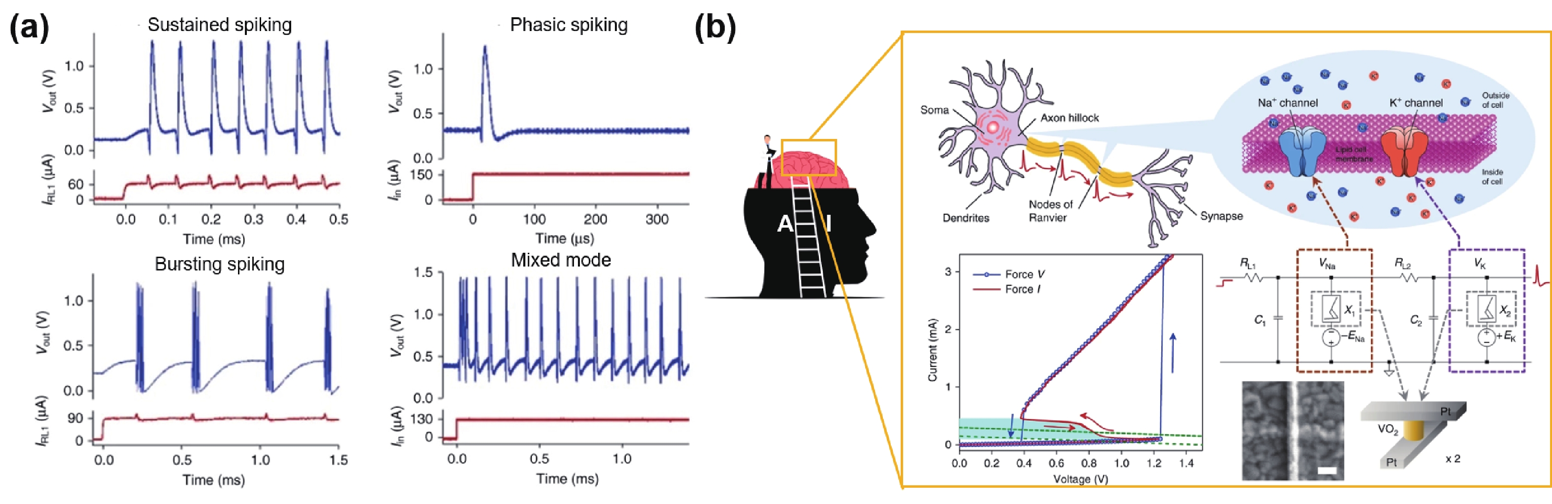
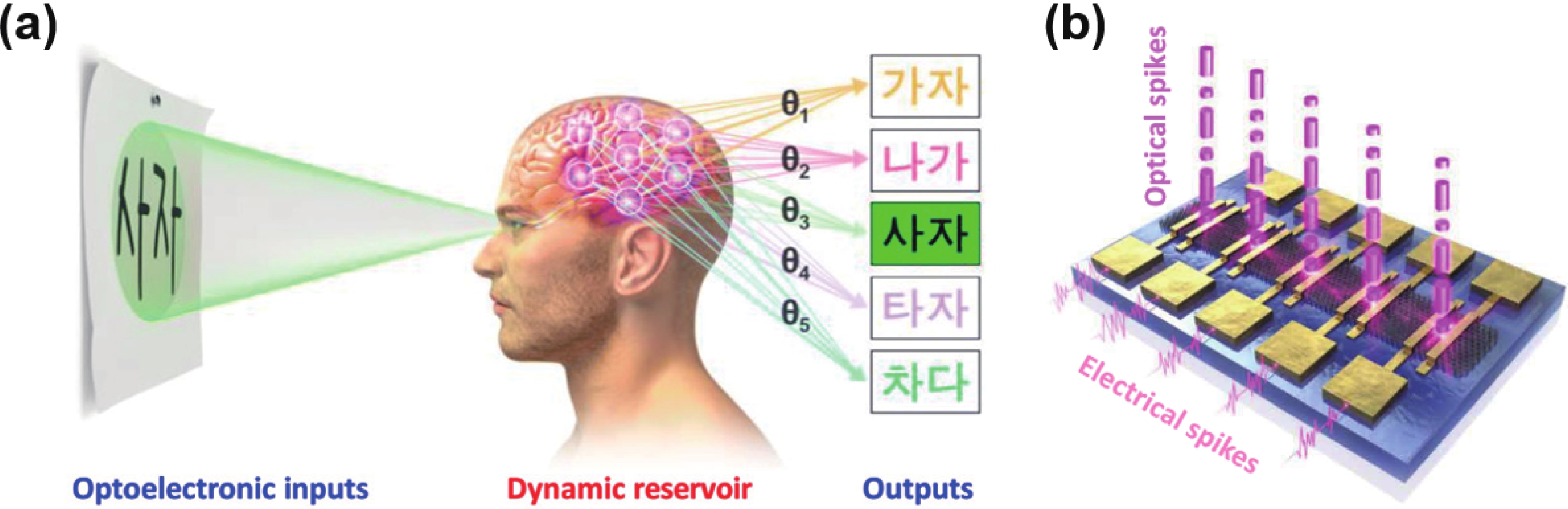
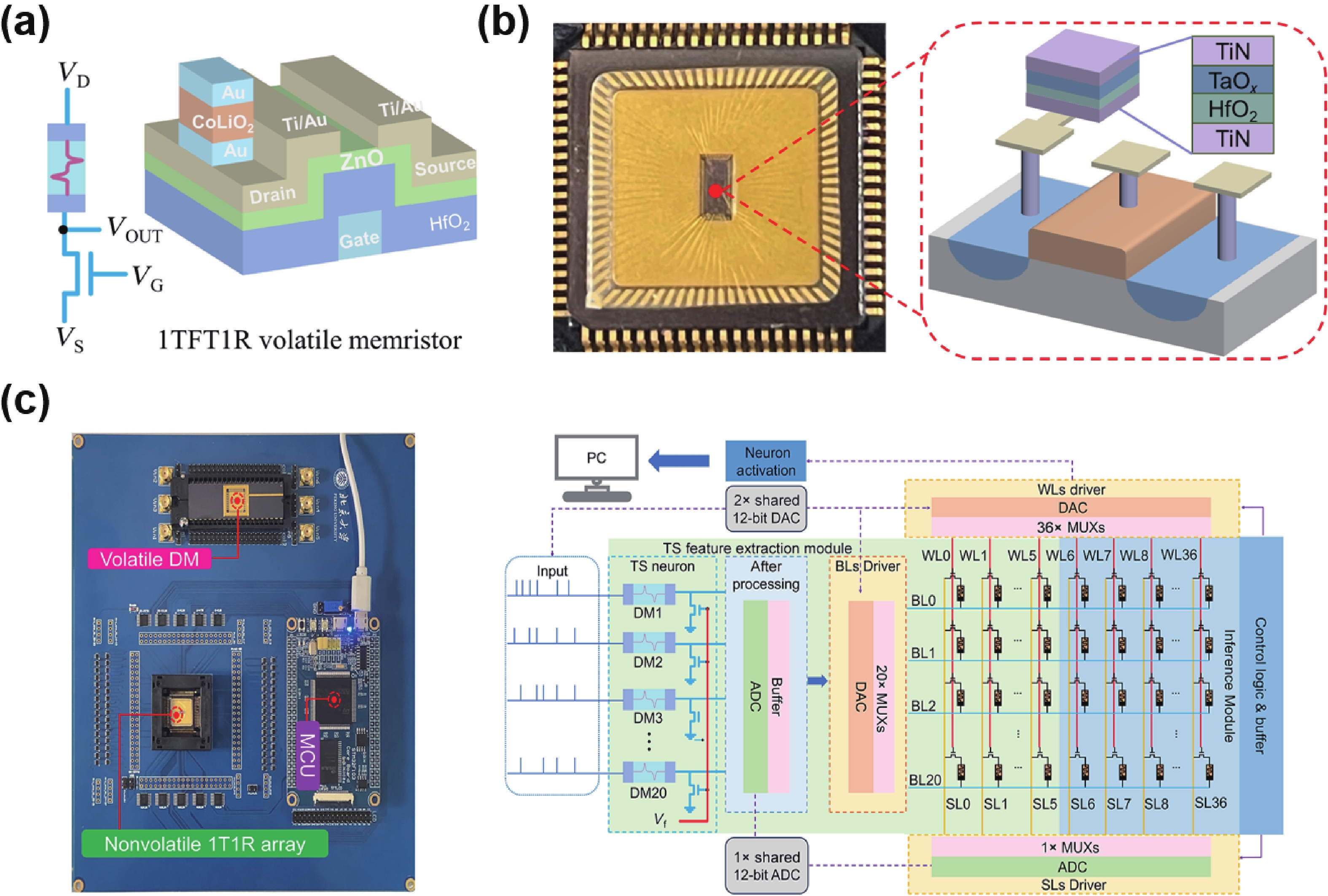
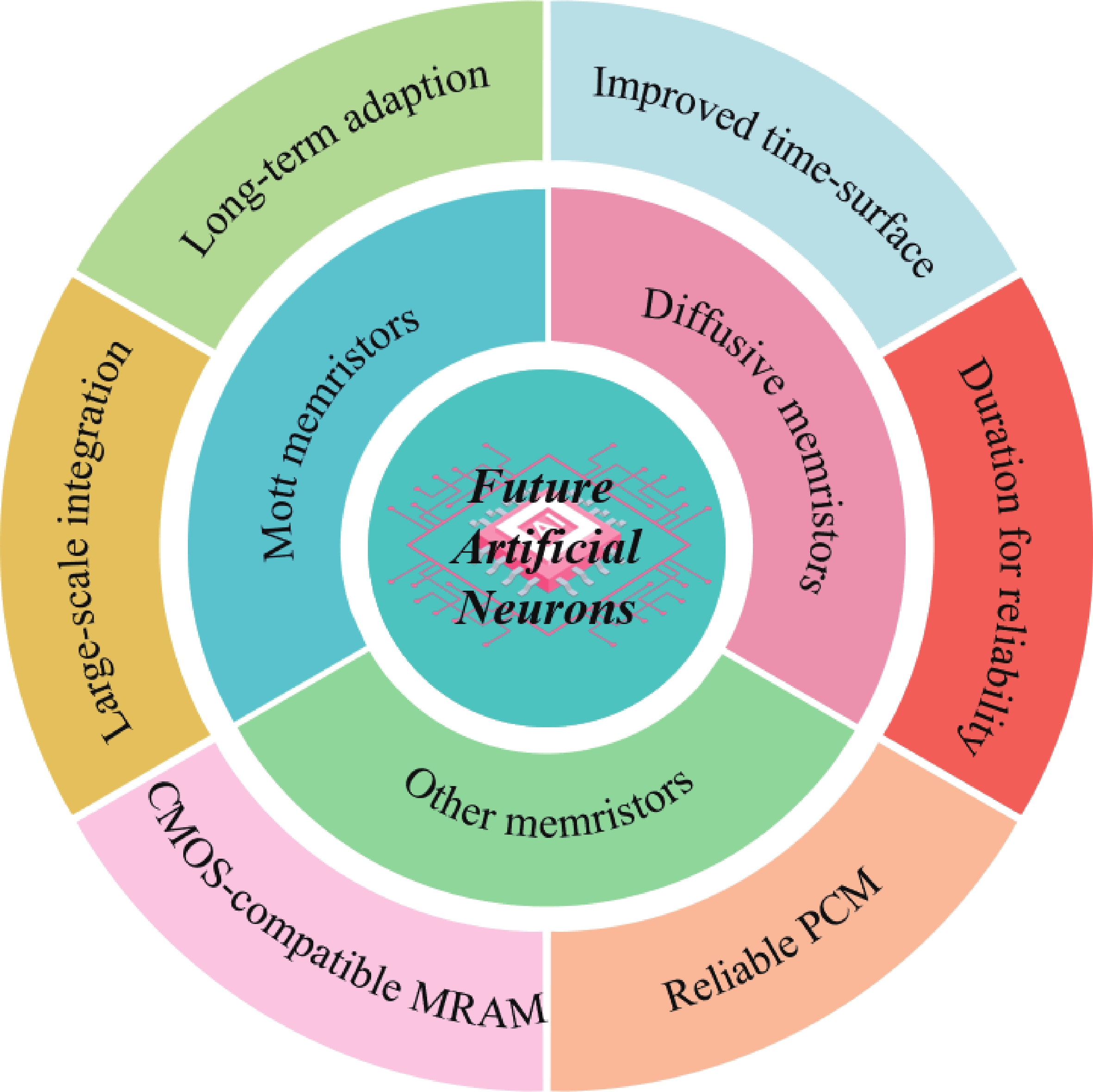
As traditional von Neumann architectures face limitations in handling the demands of big data and complex computational tasks, neuromorphic computing has emerged as a promising alternative, inspired by the human brain's neural networks. Volatile memristors, particularly Mott and diffusive memristors, have garnered significant attention for their ability to emulate neuronal dynamics, such as spiking and firing patterns, enabling the development of reconfigurable and adaptive computing systems. Recent advancements include the implementation of leaky integrate-and-fire neurons, Hodgkin−Huxley neurons, optoelectronic neurons, and time-surface neurons, all utilizing volatile memristors to achieve efficient, low-power, and highly integrated neuromorphic systems. This paper reviews the latest progress in volatile memristor-based artificial neurons, highlighting their potential for energy-efficient computing and integration with artificial synapses. We conclude by addressing challenges such as improving memristor reliability and exploring new architectures to advance memristor-based neuromorphic computing.
J. Semicond.
2025, 46(6): 061302 doi: 10.1088/1674-4926/24100010

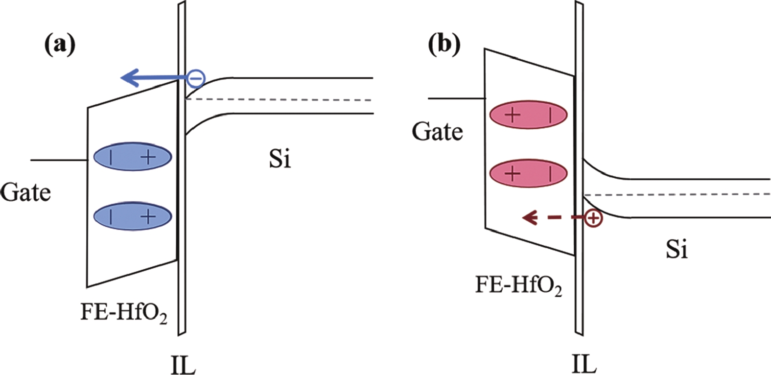
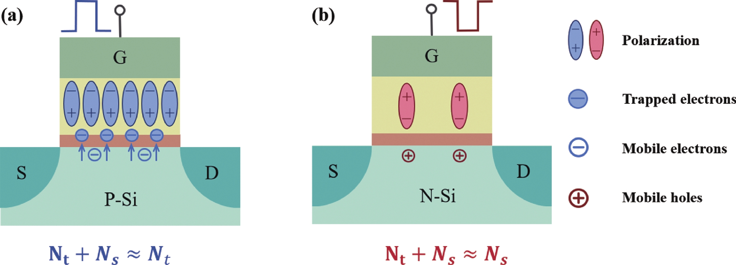
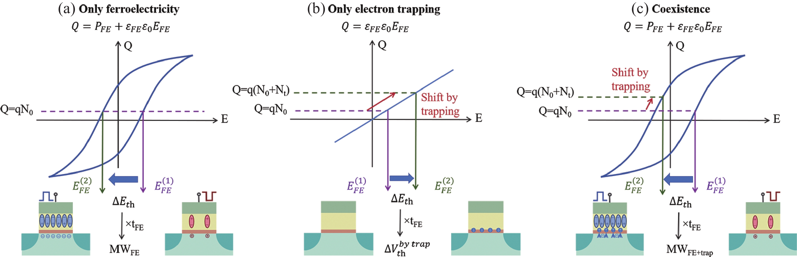
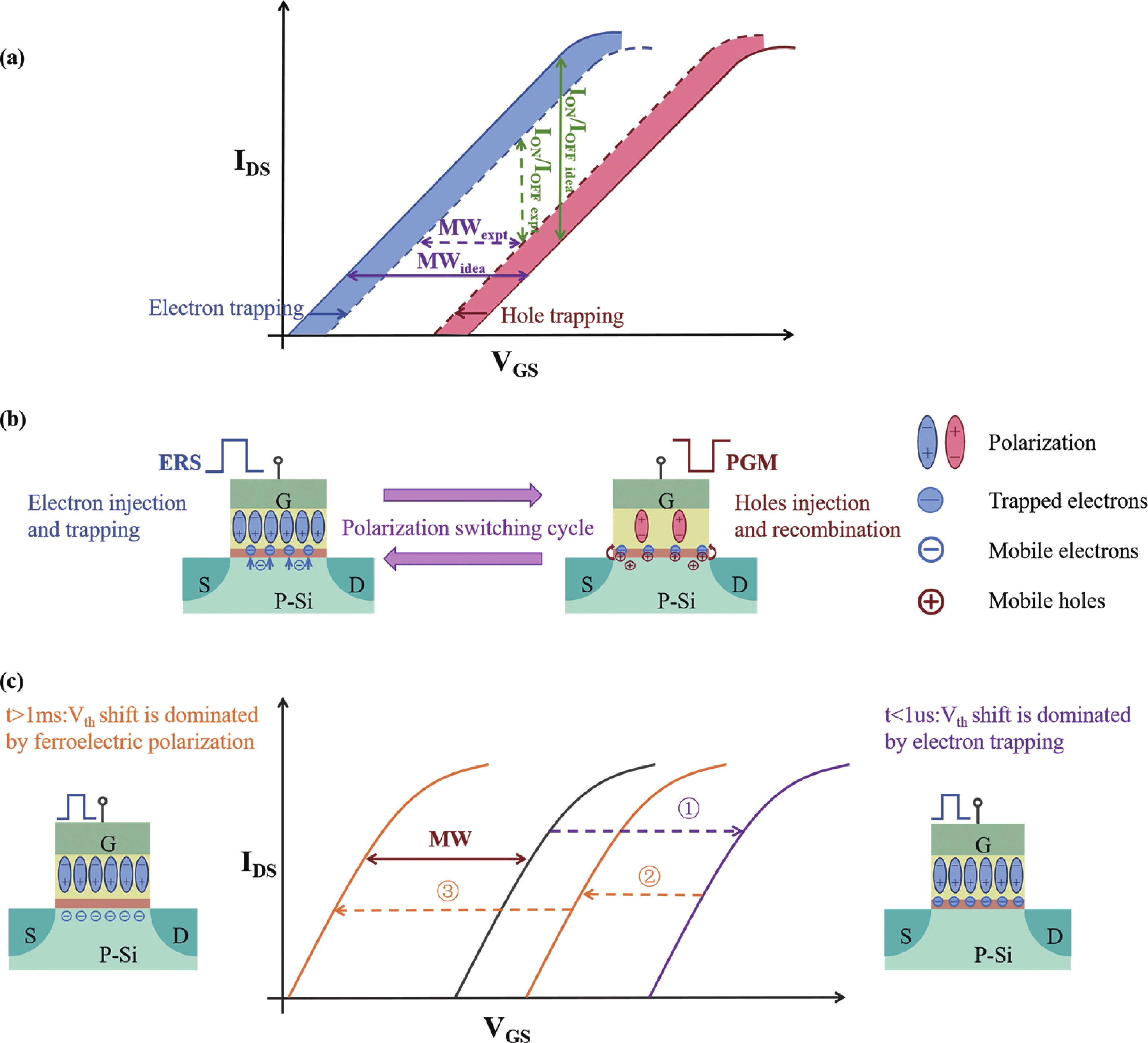
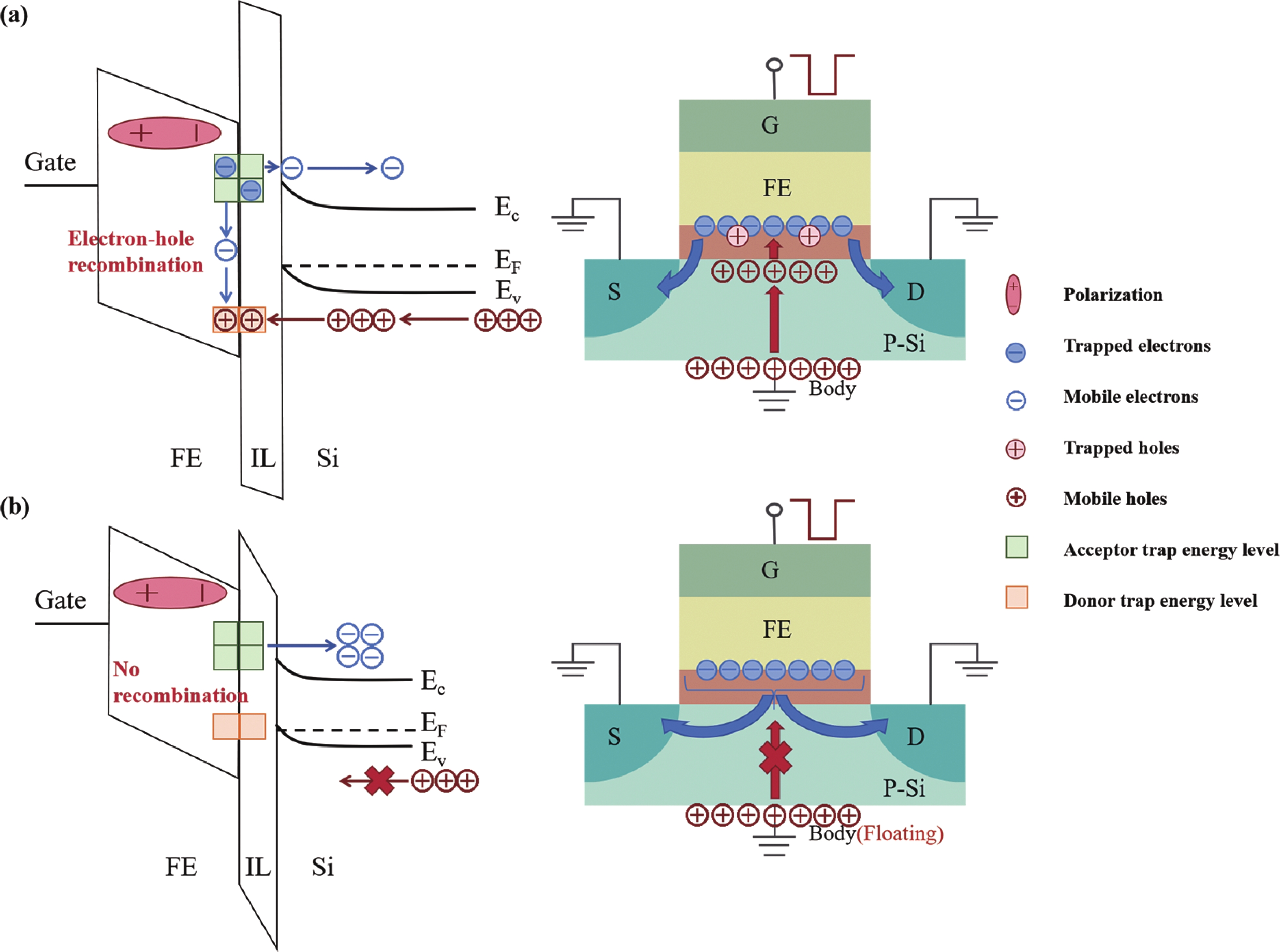
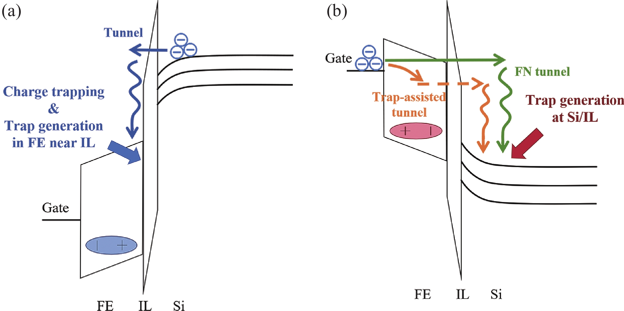
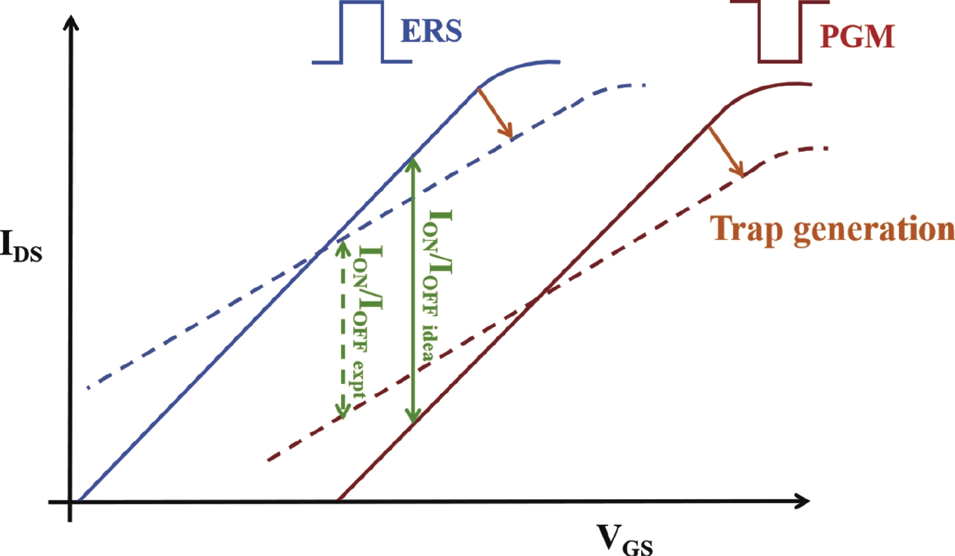
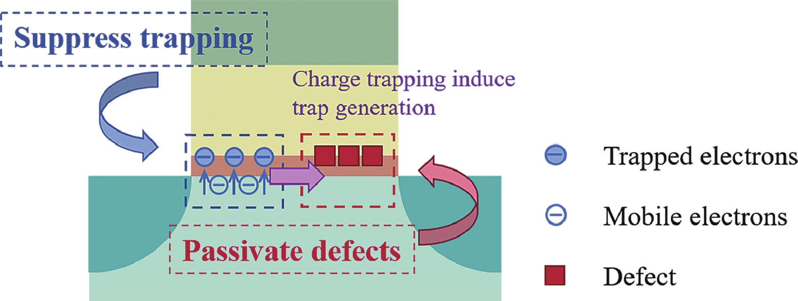
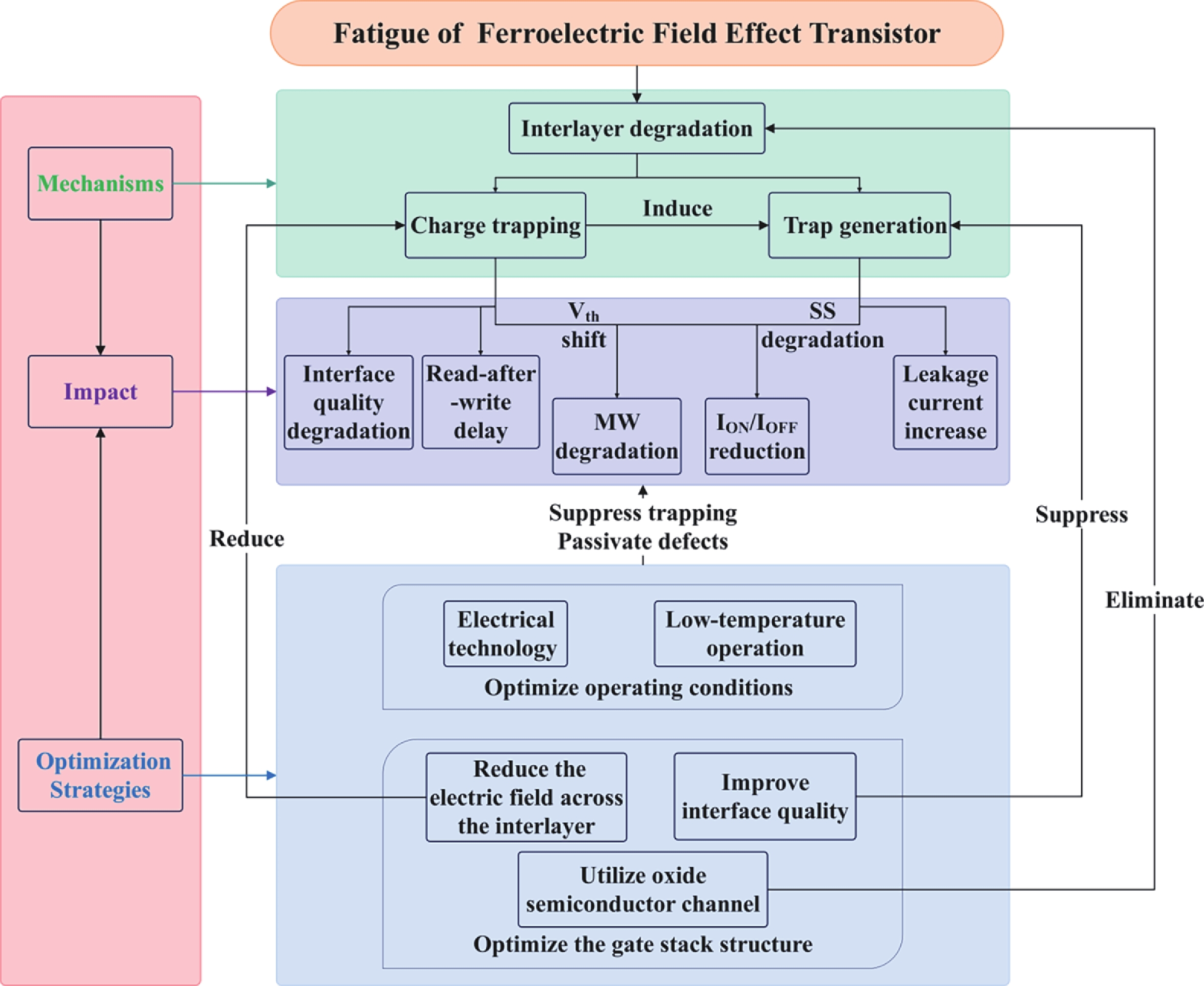
The novel HfO2-based ferroelectric field effect transistor (FeFET) is considered a promising candidate for next-generation nonvolatile memory (NVM). However, a series of reliability issues caused by the fatigue effect hinder its further development. Therefore, a comprehensive understanding of the fatigue mechanisms of the device and optimization strategies is essential for its application. The fundamental mechanism of the fatigue effect is attributed to charge trapping and trap generation based on the current studies, and the underlying causes, occurrence locations and specific impacts are analyzed in this review. In particular, the asymmetric trapping/detrapping of electrons and holes, as well as the relationship between the ferroelectric (FE) polarization and charge trapping, are given particular attention. After categorizing and summarizing the current progress, we propose a series of optimization strategies derived based on the fatigue mechanisms.
Intensity correlation distribution in gain-switched semiconductor laser for quantum key distribution
J. Semicond.
2025, 46(6): 062101 doi: 10.1088/1674-4926/24090052
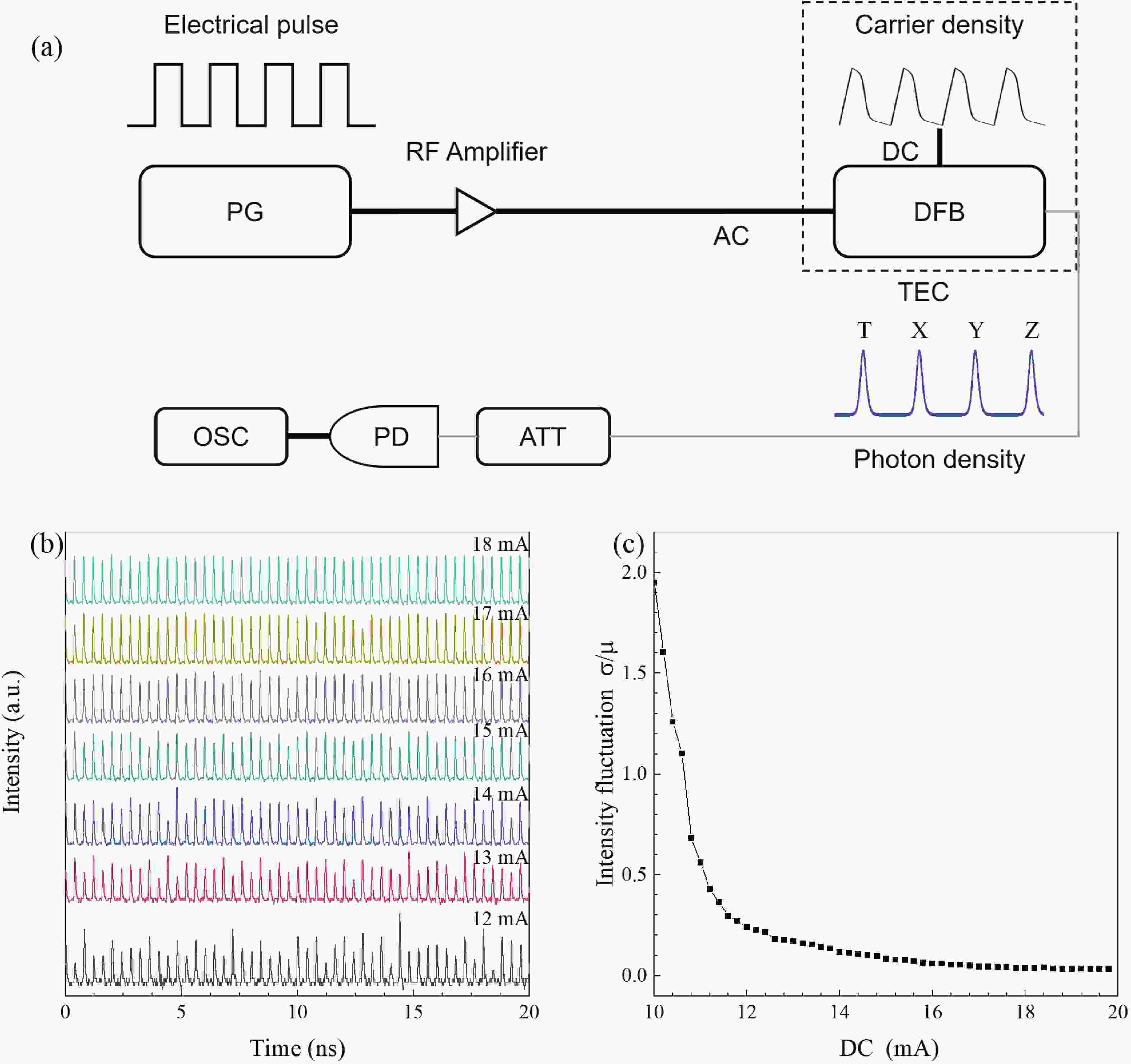
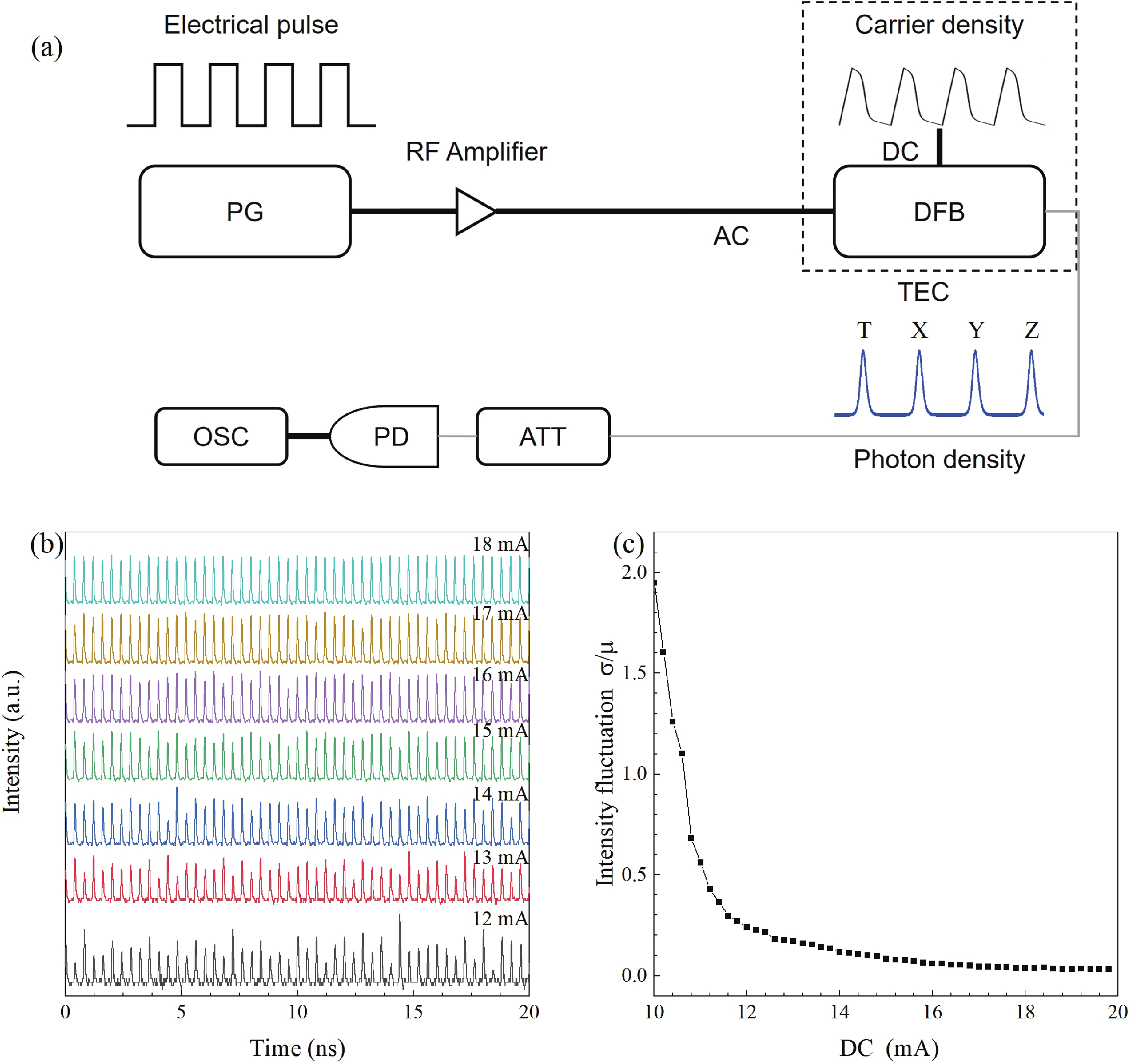
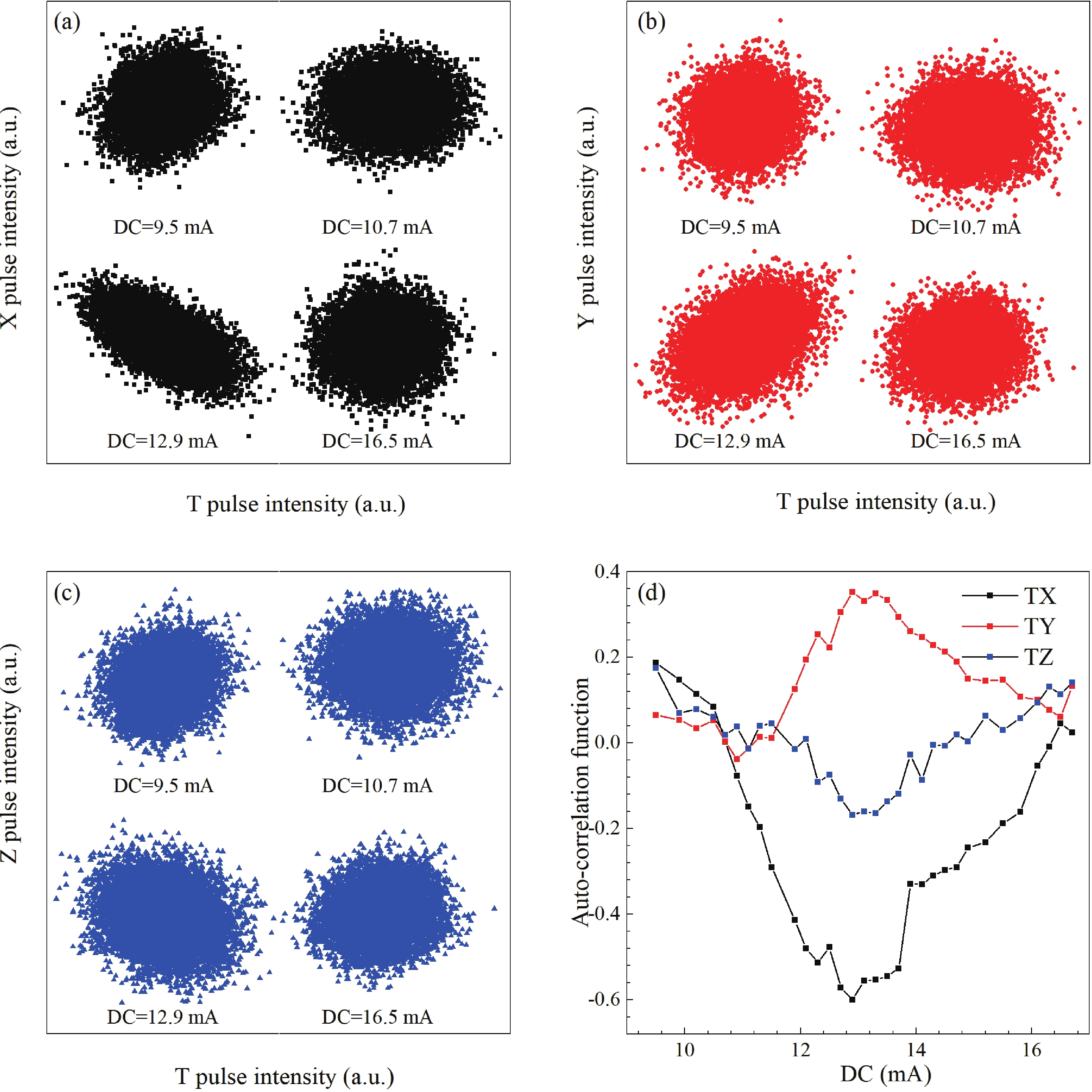
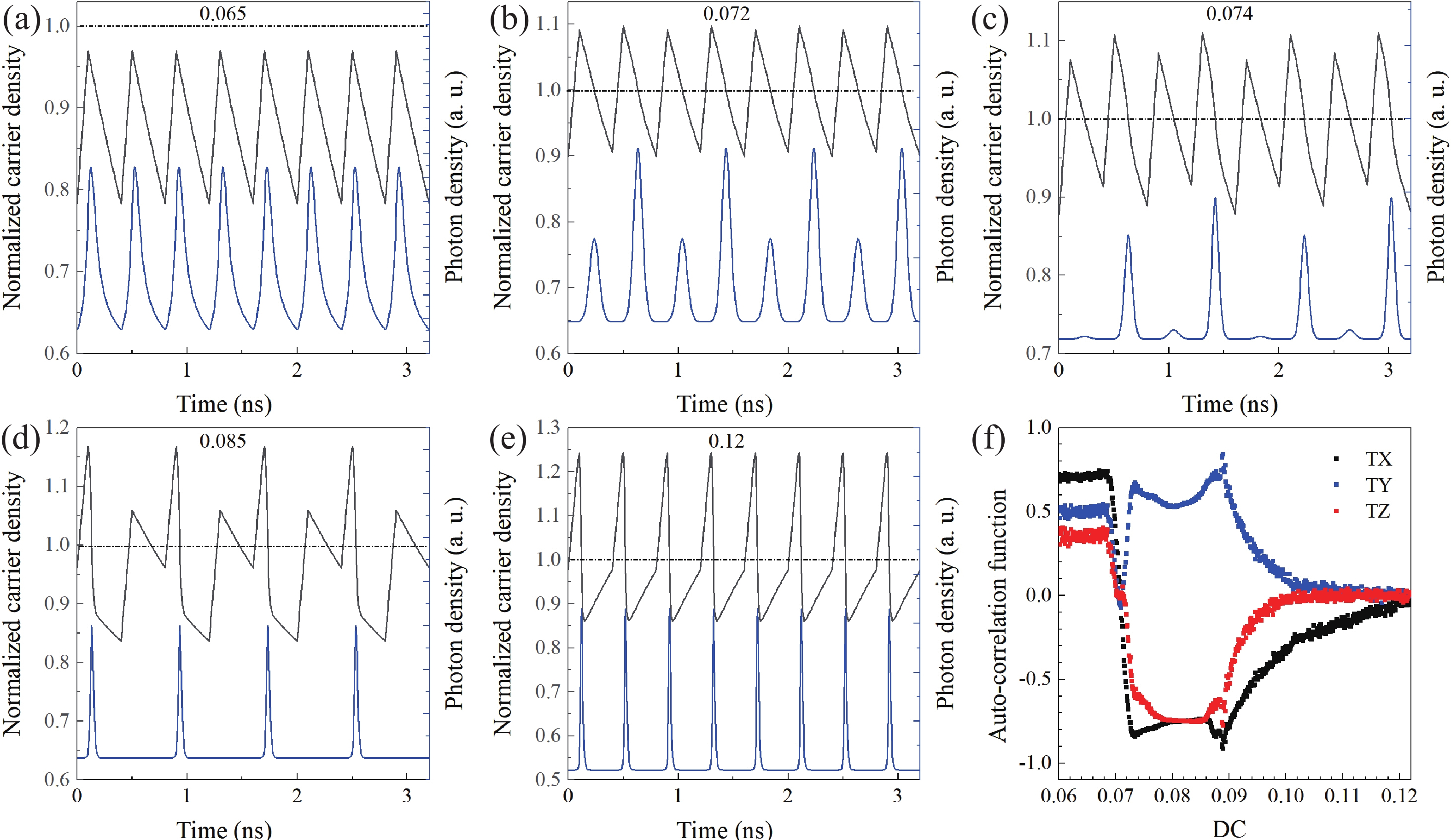
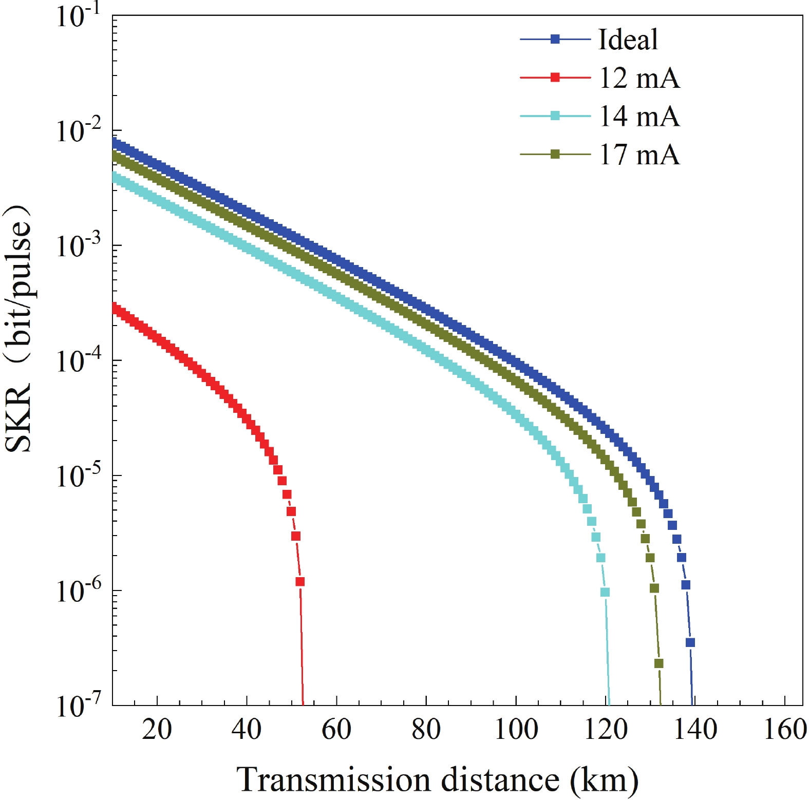
In the implementation of quantum key distribution, Security certification is a prerequisite for social deployment. Transmitters in decoy-BB84 systems typically employ gain-switched semiconductor lasers (GSSLs) to generate optical pulses for encoding quantum information. However, the working state of the laser may violate the assumption of pulse independence. Here, we explored the dependence of intensity fluctuation and high-order correlation distribution of optical pulses on driving currents at 2.5 GHz. We found the intensity correlation distribution had a significant dependence on the driving currents, which would affect the final key rate. By utilizing rate equations in our simulation, we confirmed the fluctuation and correlation originated from the instability of gain-switched laser driven at a GHz-repetitive frequency. Finally, we evaluated the impact of intensity fluctuation on the secure key rate. This work will provide valuable insights for assessing whether the transmitter is operating at optimal state in practice.
J. Semicond.
2025, 46(6): 062301 doi: 10.1088/1674-4926/24100018
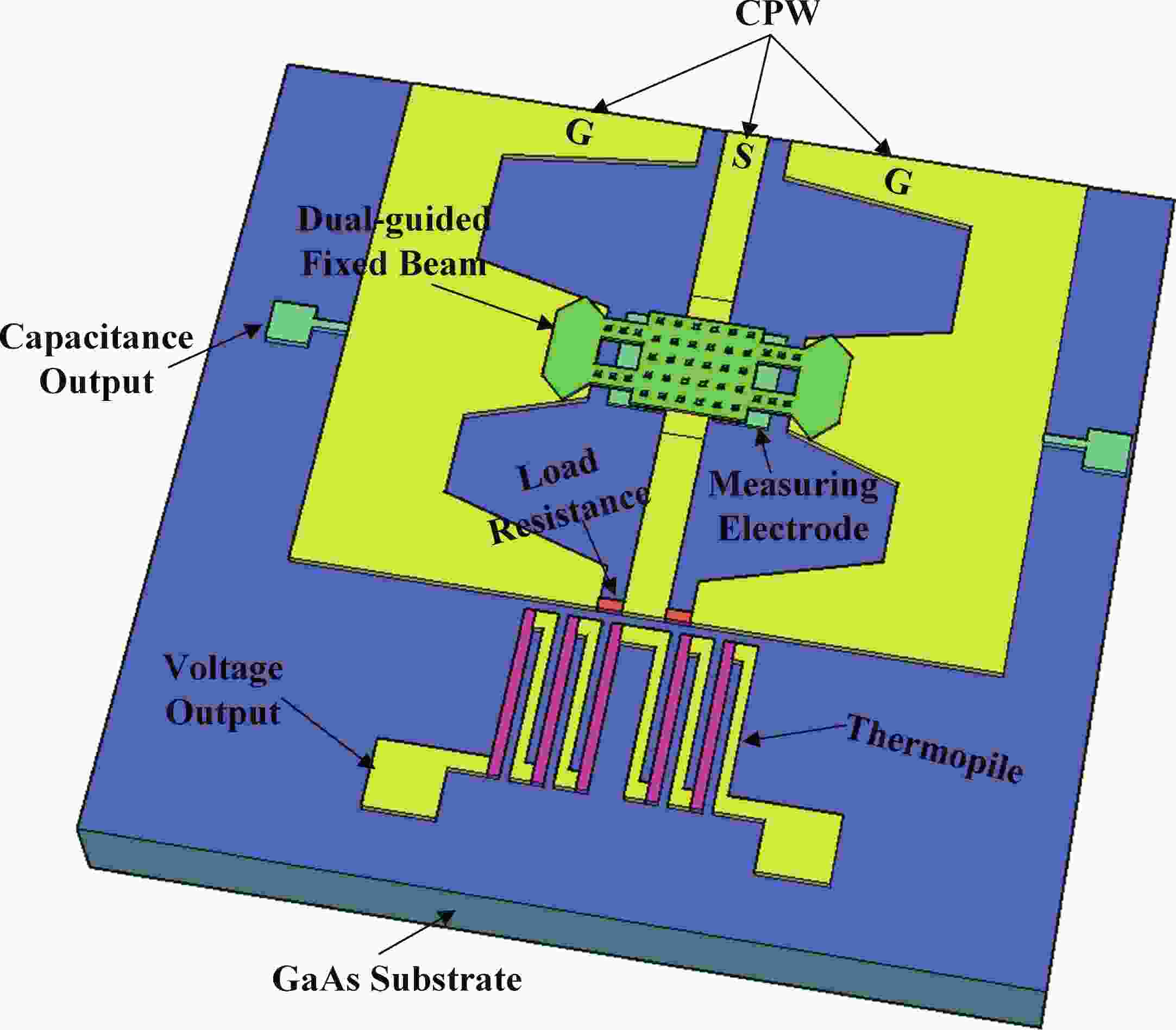
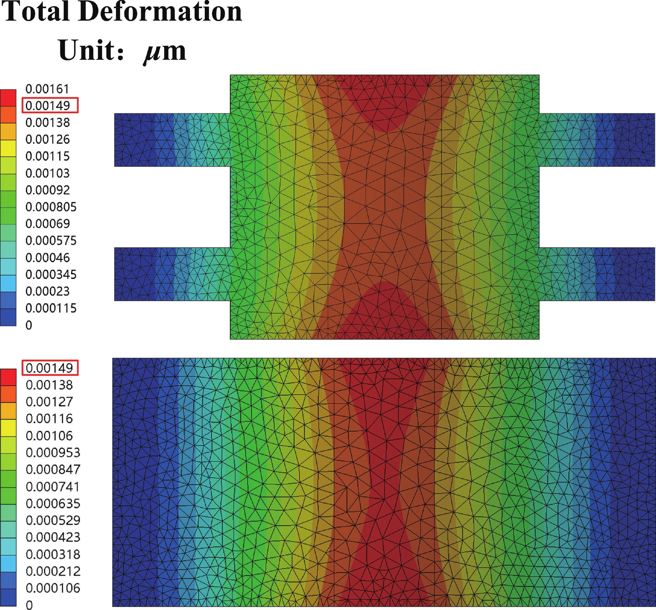
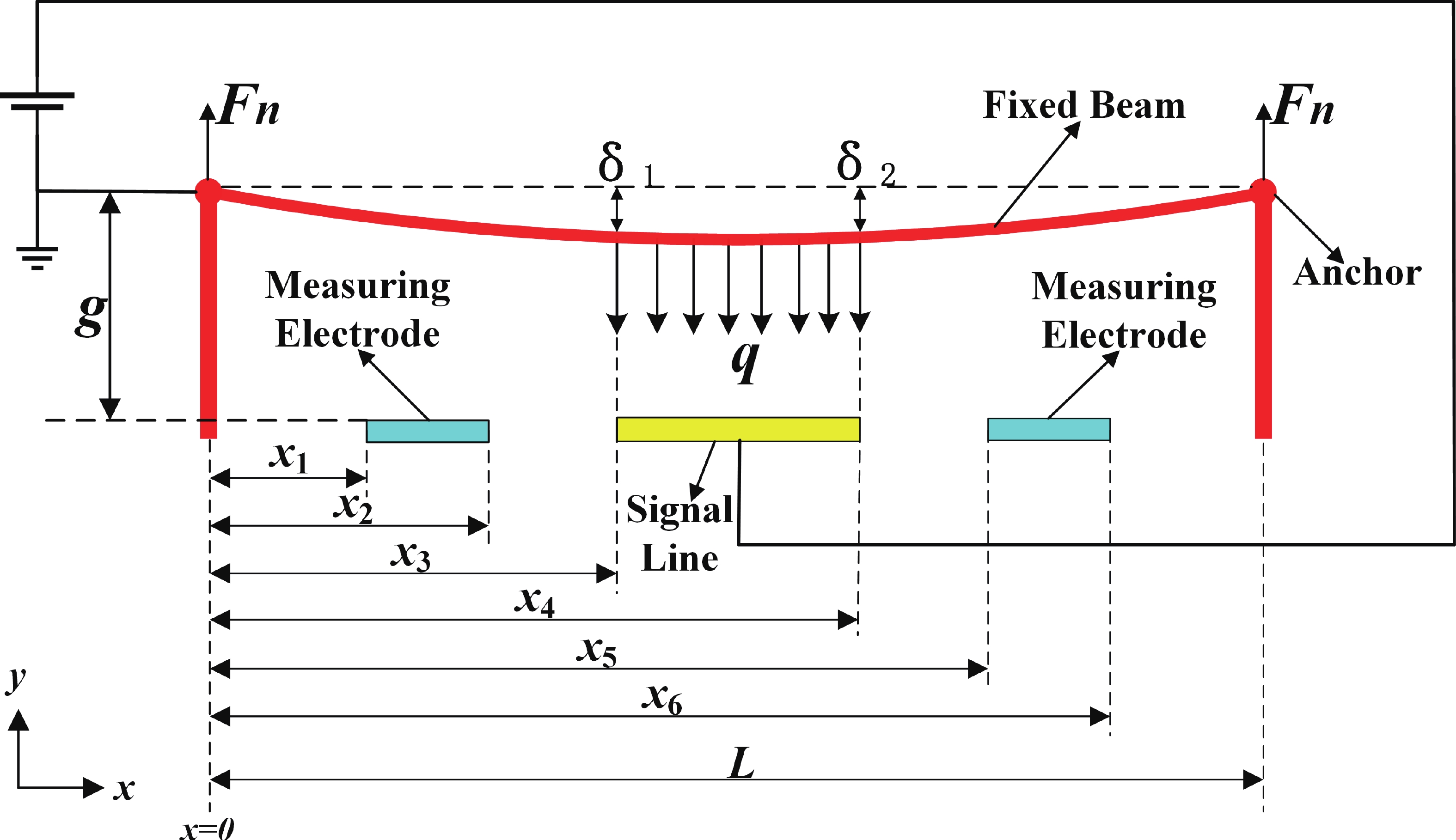
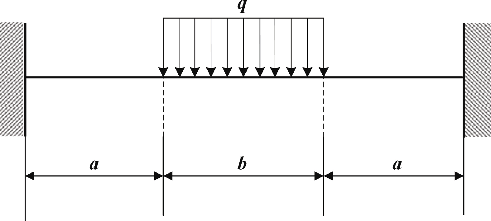
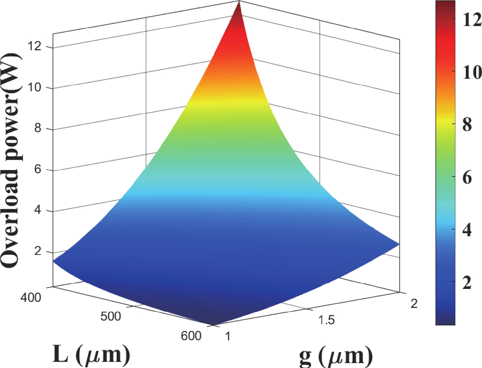
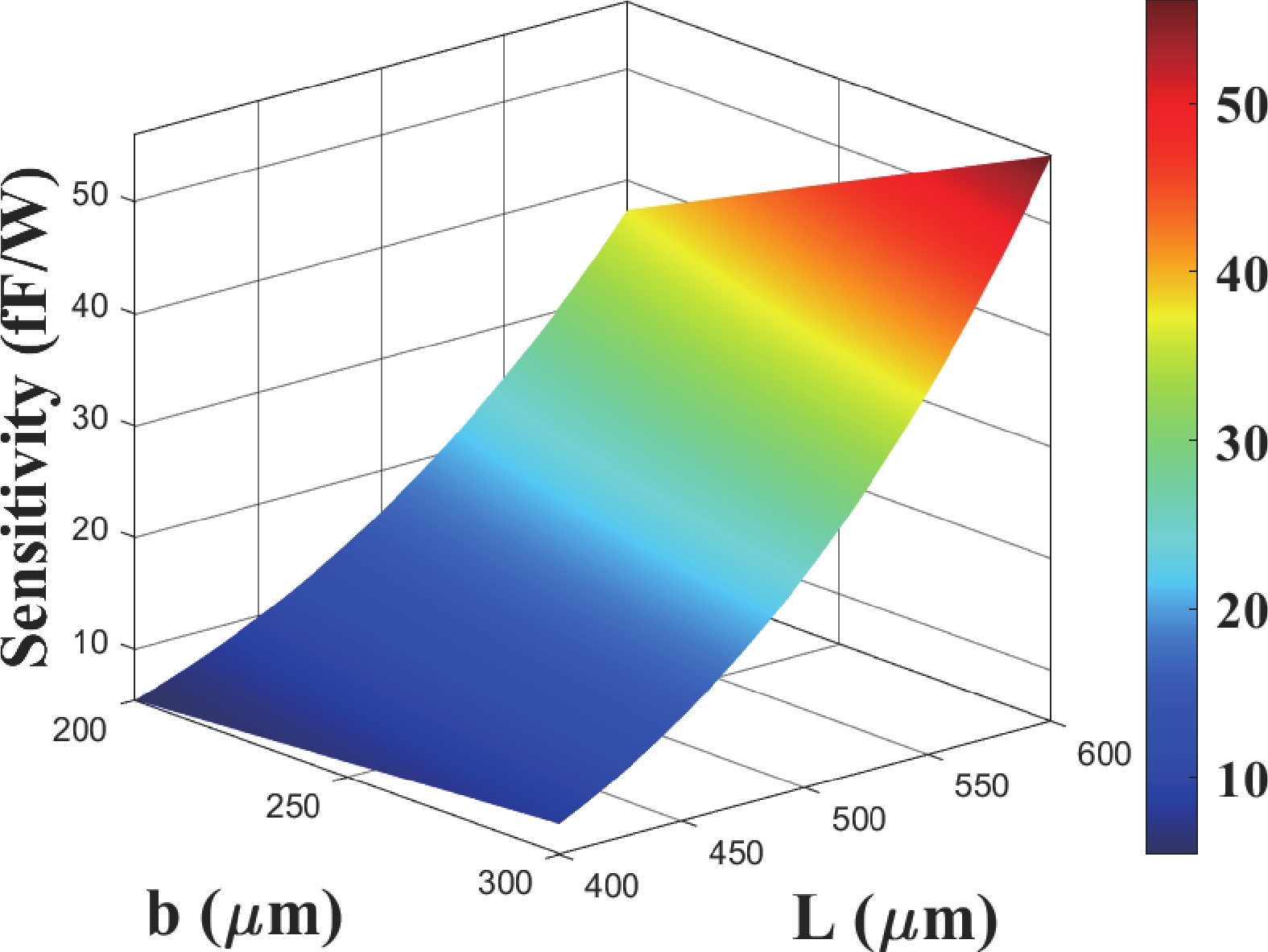
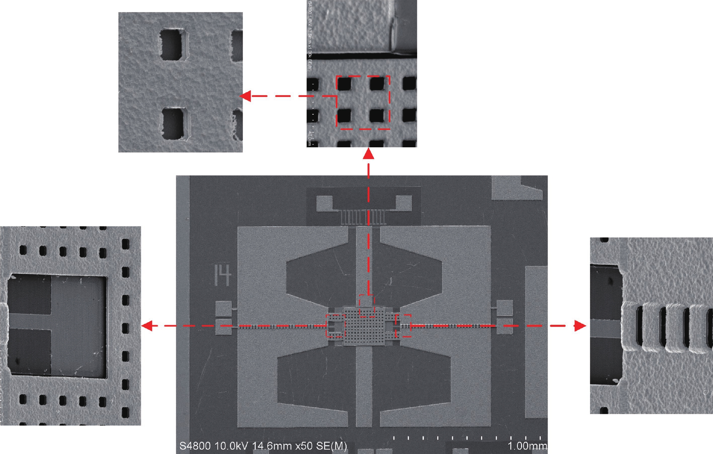
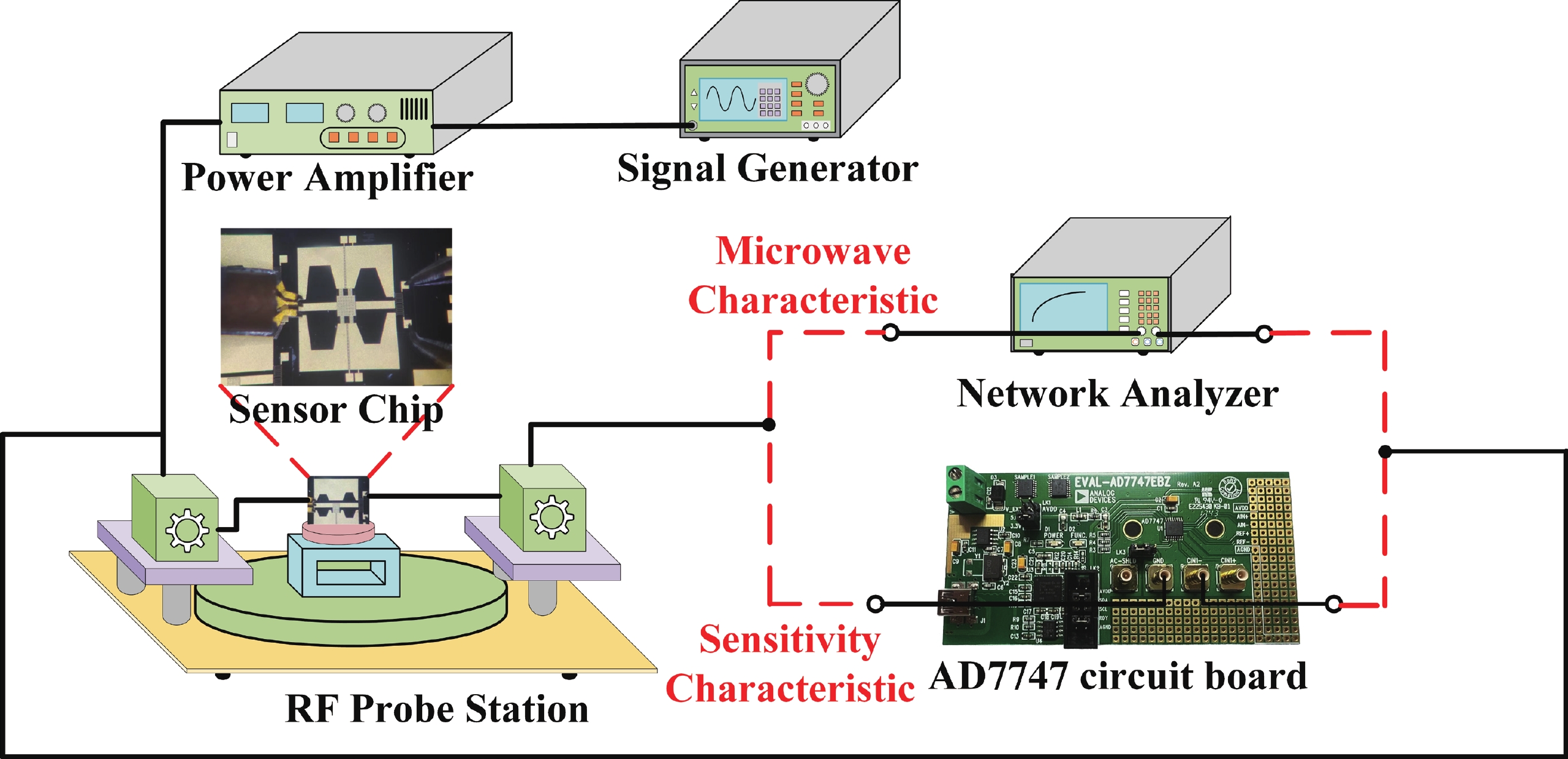
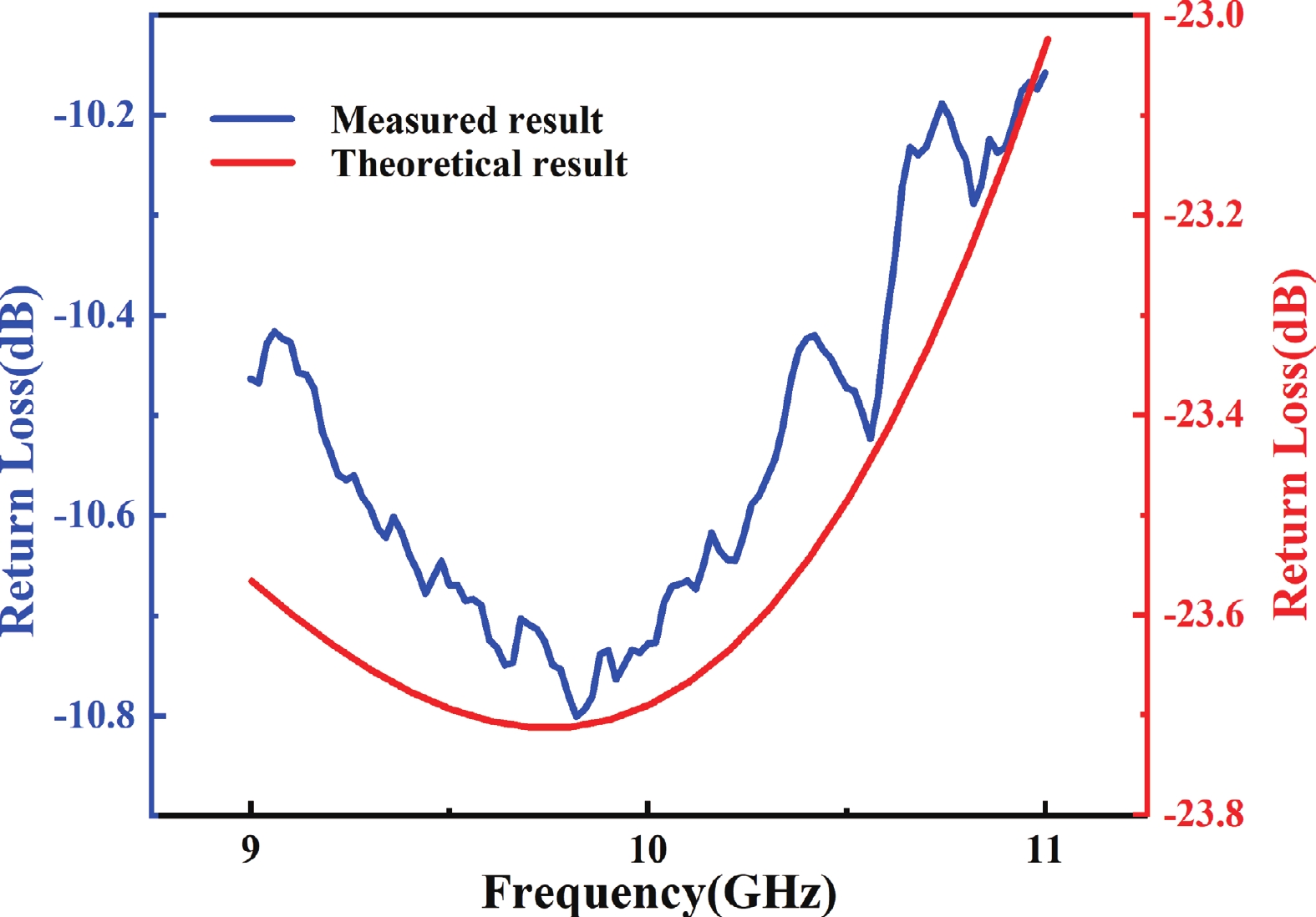
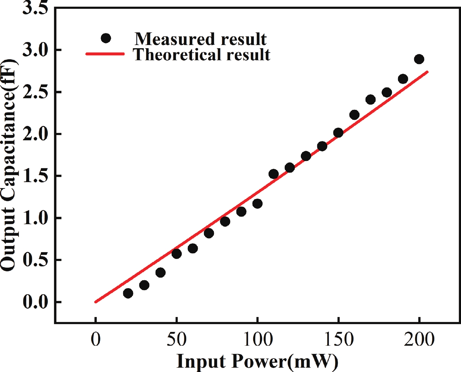
In order to solve the problems of low overload power in MEMS cantilever beams and low sensitivity in traditional MEMS fixed beams, a novel MEMS microwave power detection chip based on the dual-guided fixed beam is designed. A gap between guiding beams and measuring electrodes is designed to accelerate the release of the sacrificial layer, effectively enhancing chip performance. A load sensing model for the MEMS fixed beam microwave power detection chip is proposed, and the mechanical characteristics are analyzed based on the uniform load applied. The overload power and sensitivity are investigated using the load sensing model, and experimental results are compared with theoretical results. The detection chip exhibits excellent microwave characteristic in the 9−11 GHz frequency band, with a return loss less than −10 dB. At a signal frequency of 10 GHz, the theoretical sensitivity is 13.8 fF/W, closely matching the measured value of 14.3 fF/W, with a relative error of only 3.5%. These results demonstrate that the proposed load sensing model provides significant theoretical support for the design and performance optimization of MEMS microwave power detection chips.
J. Semicond.
2025, 46(6): 062302 doi: 10.1088/1674-4926/24070029
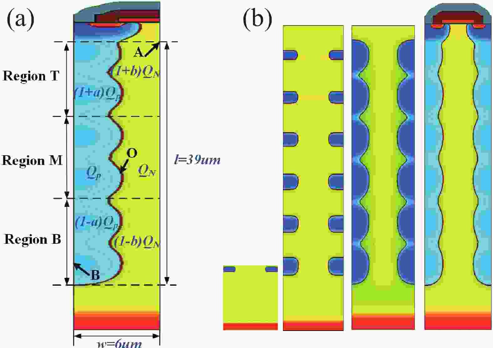
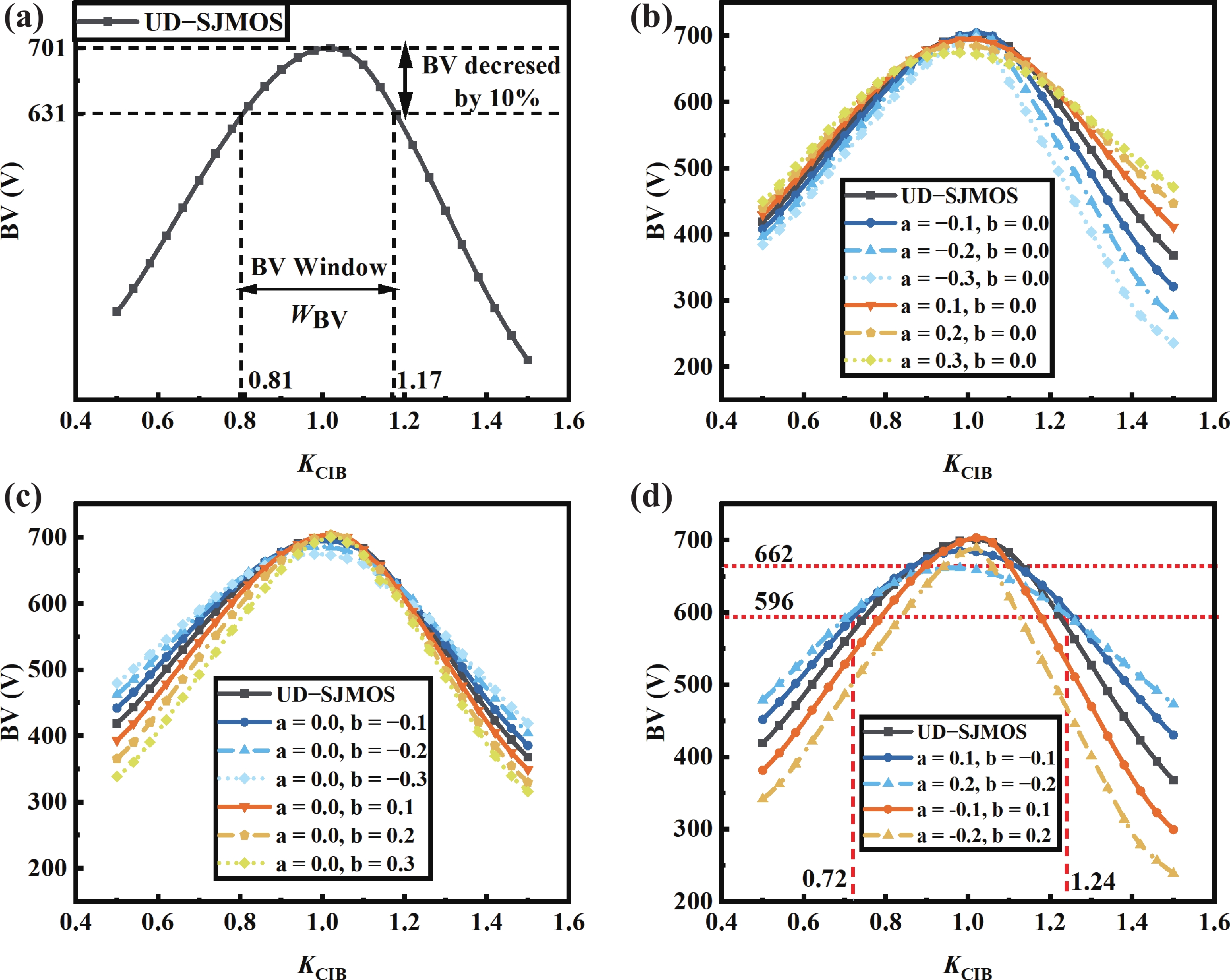
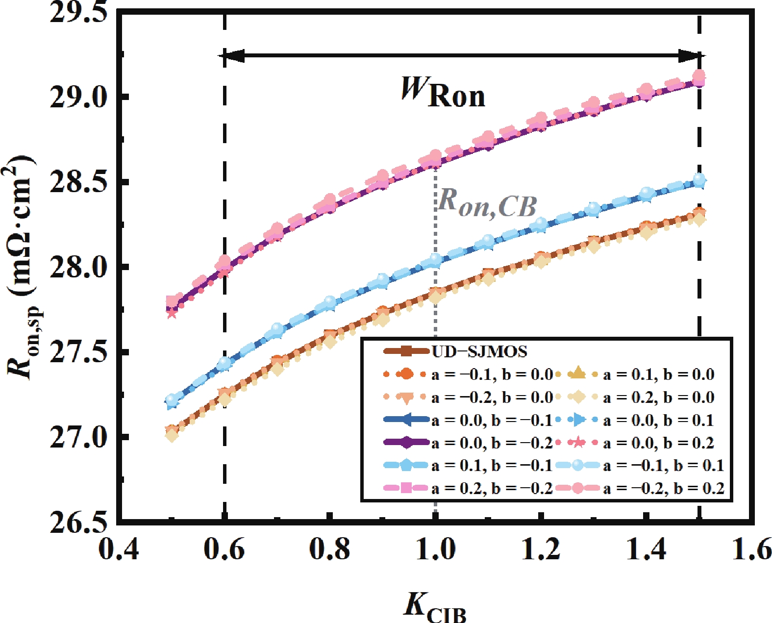
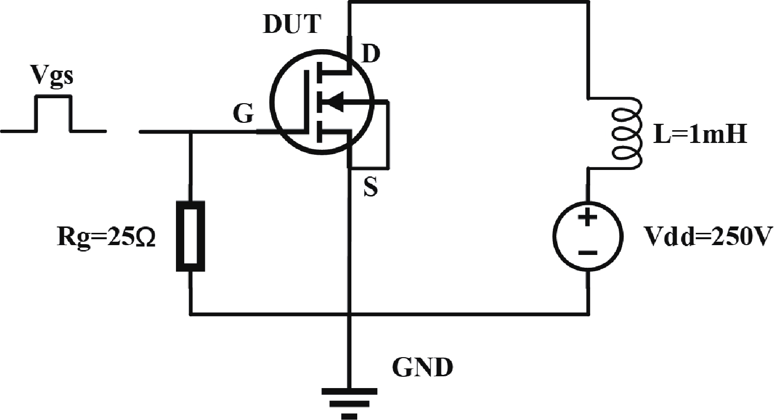
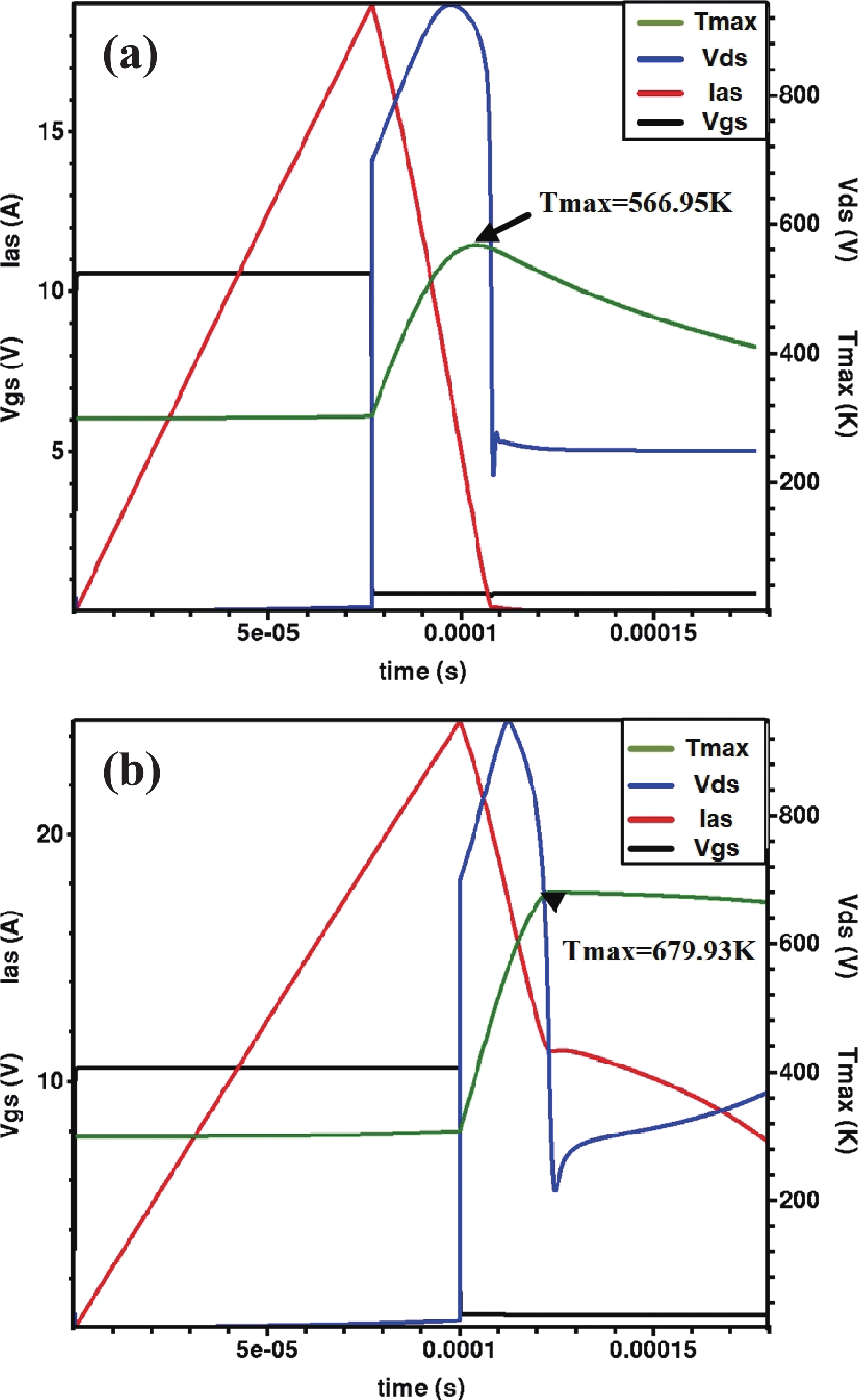
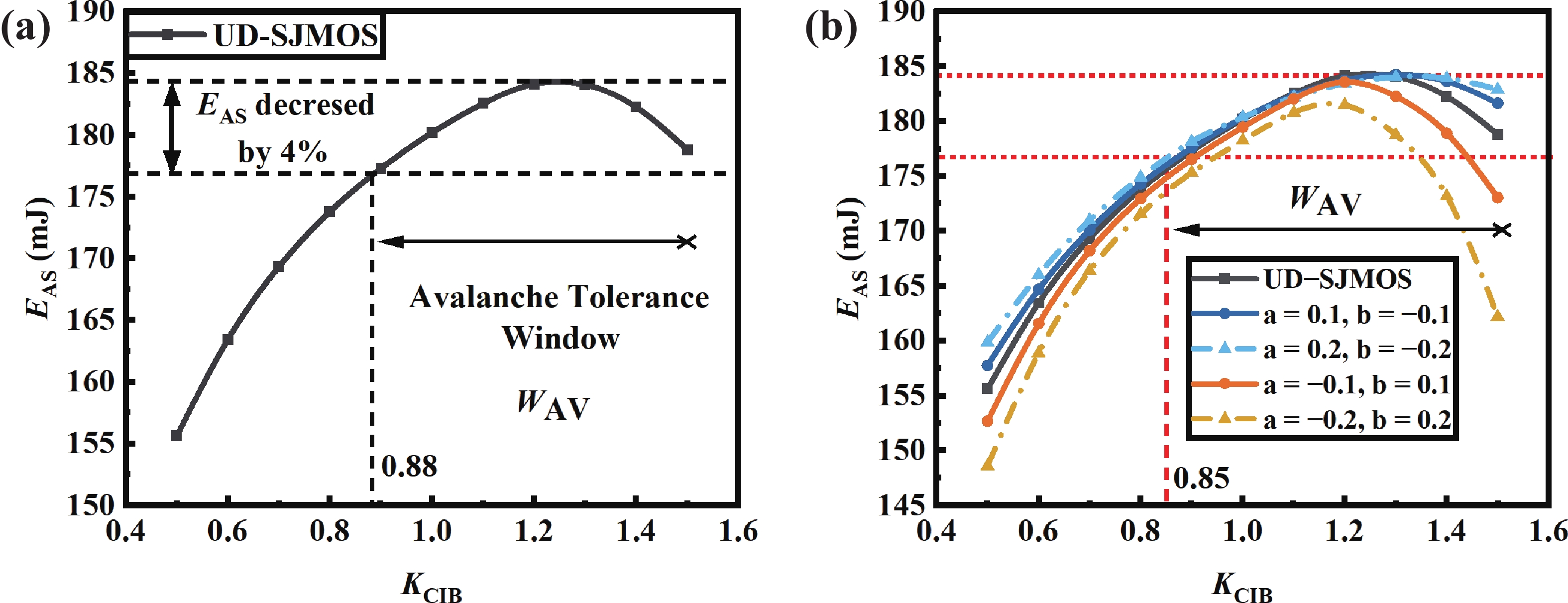
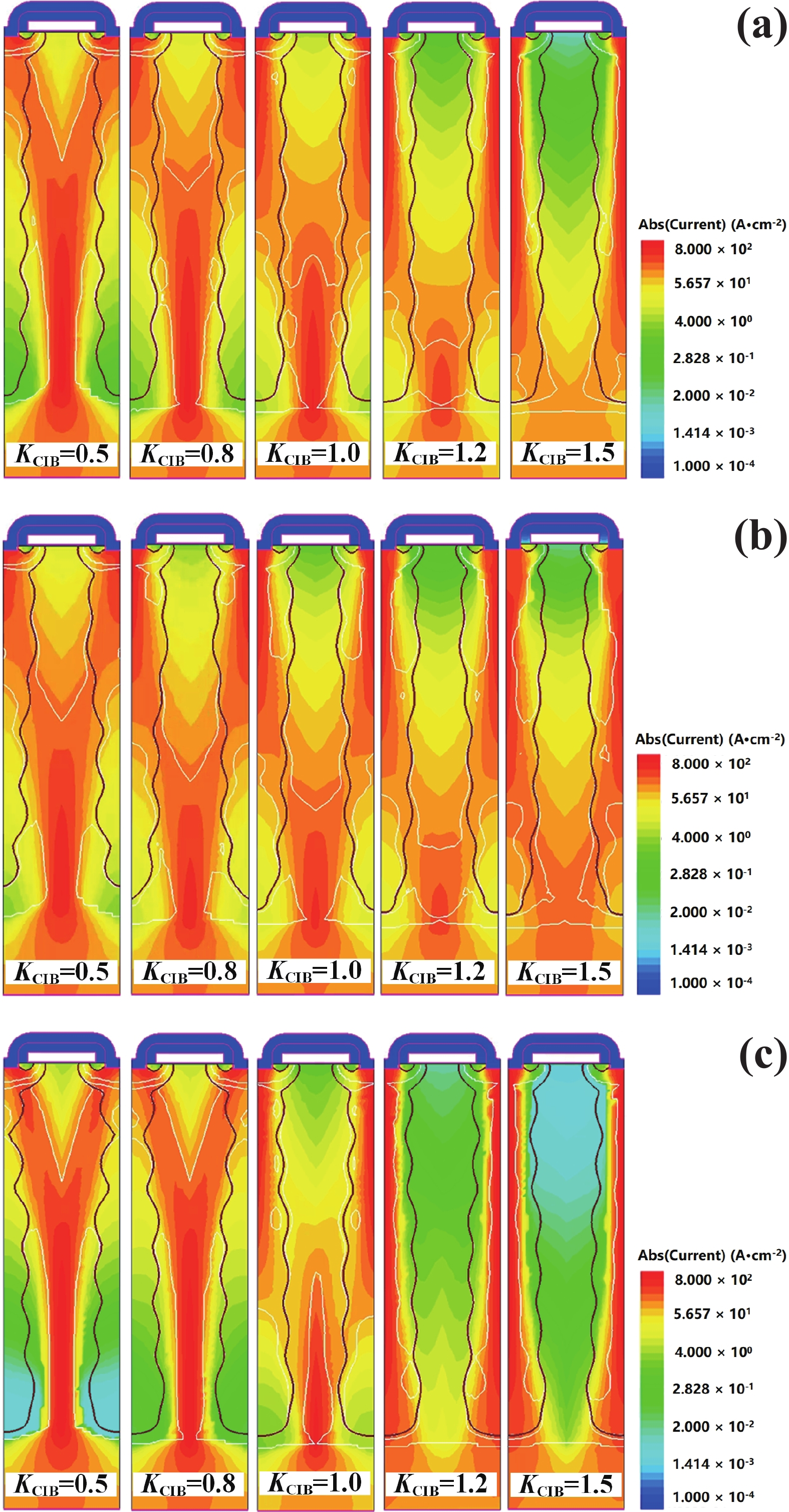
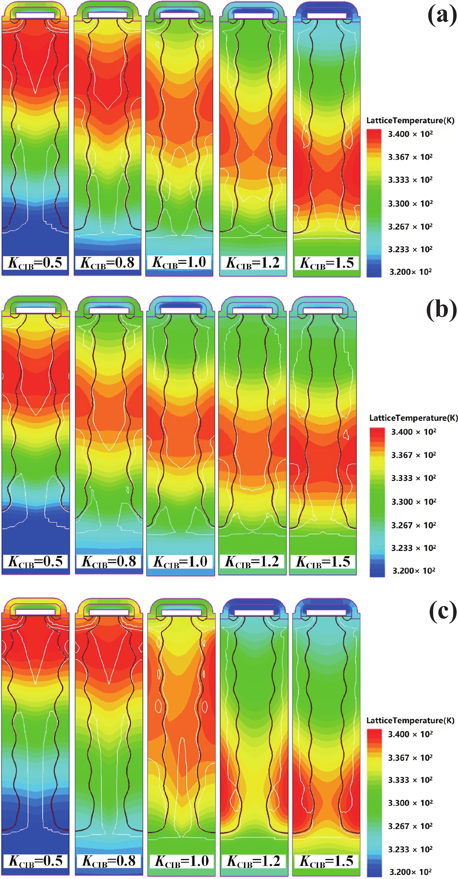
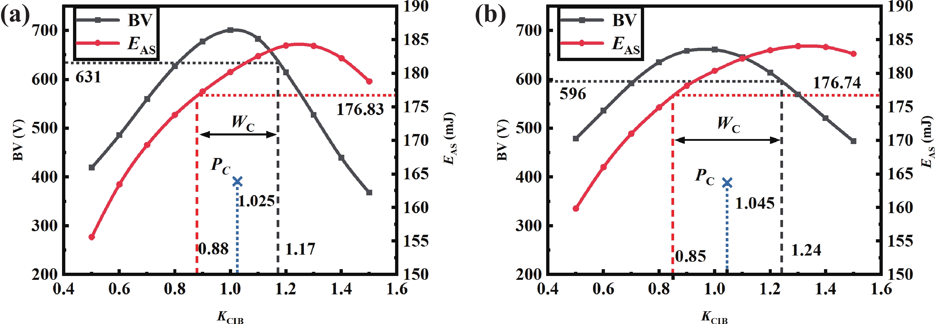
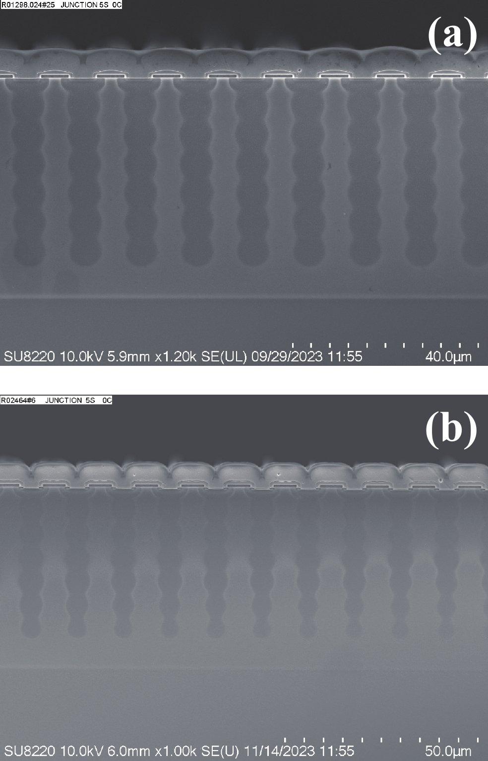
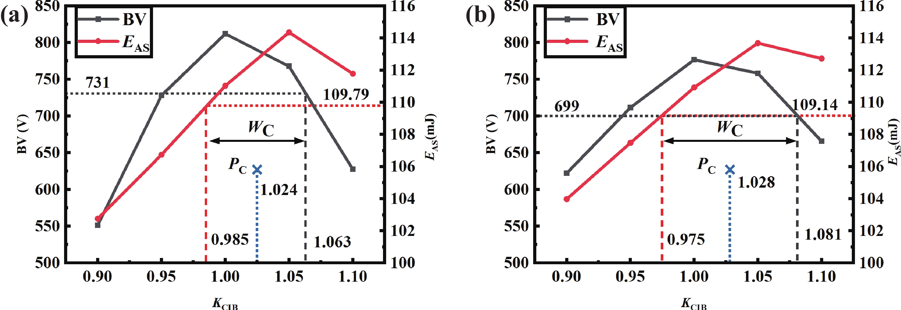
As a type of charge-balanced power device, the performance of super-junction MOSFETs (SJ-MOS) is significantly influenced by fluctuations in the fabrication process. To overcome the relatively narrow process window of conventional SJ-MOS, an optimized structure "vertical variable doping super-junction MOSFET (VVD-SJ)" is proposed. Based on the analysis using the charge superposition principle, it is observed that the VVD-SJ, in which the impurity concentration of the P-pillar gradually decreases while that of the N-pillar increases from top to bottom, improves the electric field distribution and mitigates charge imbalance (CIB). Experimental results demonstrate that the optimized 600 V VVD-SJ achieves a 35.90% expansion of the process window.

J. Semicond.
2025, 46(6): 062303 doi: 10.1088/1674-4926/24090040
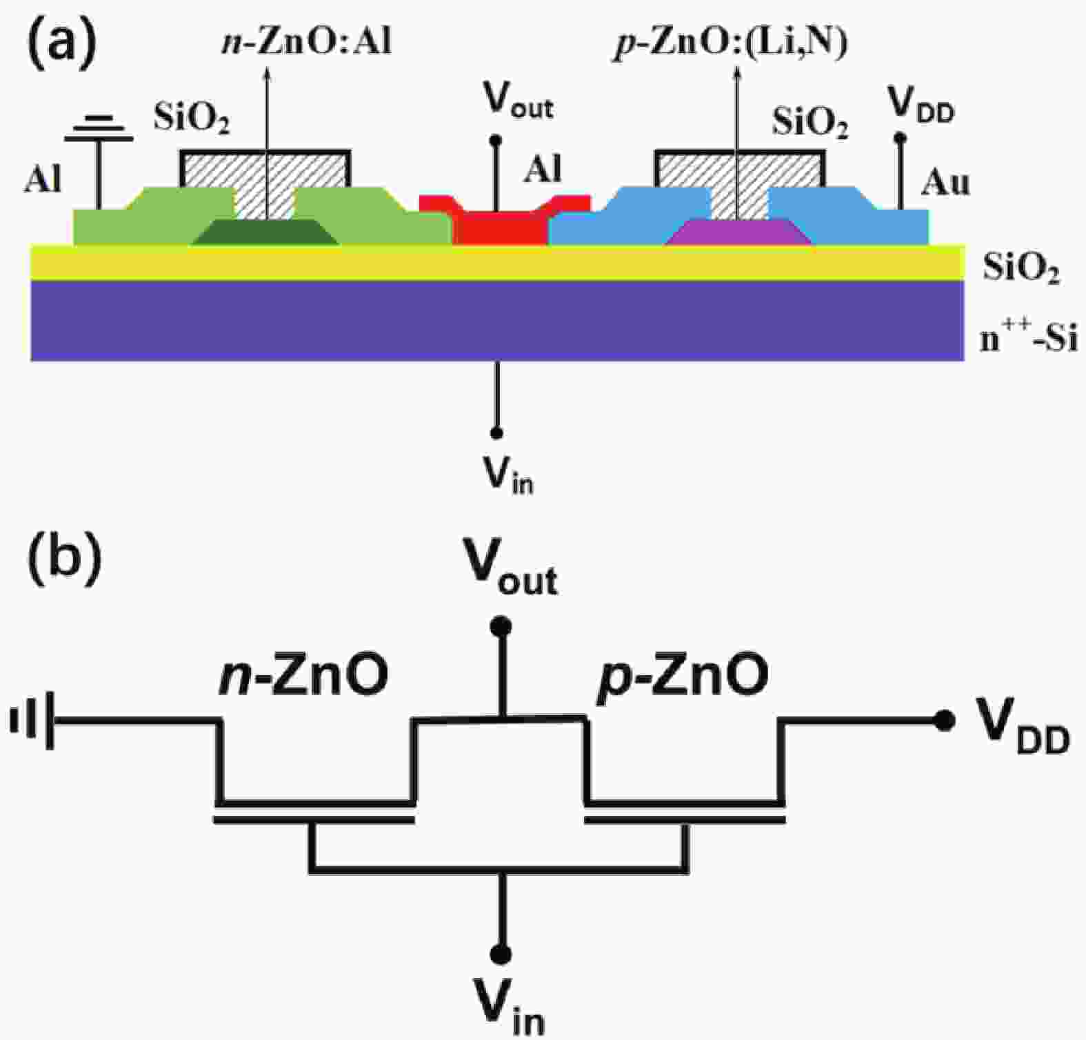
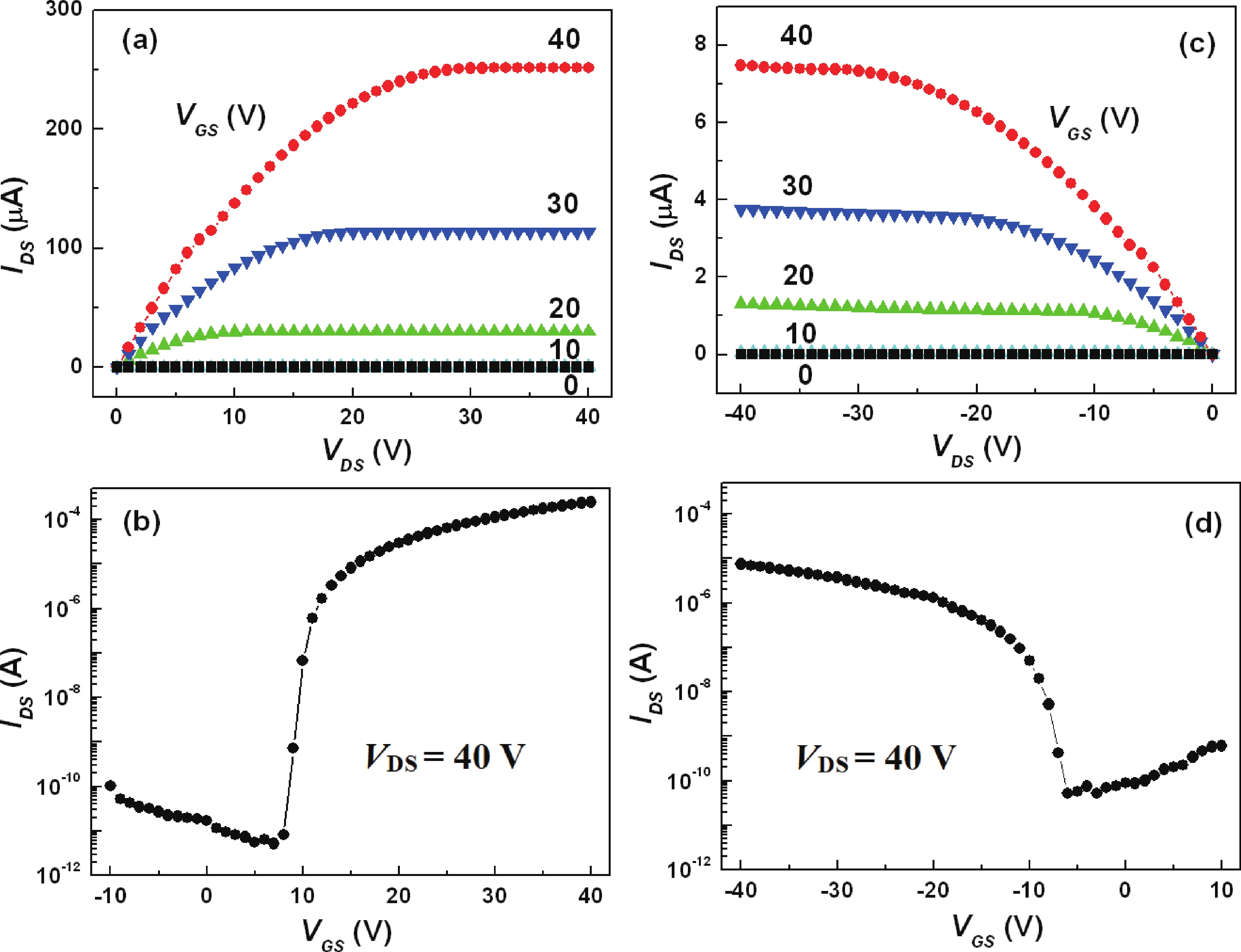
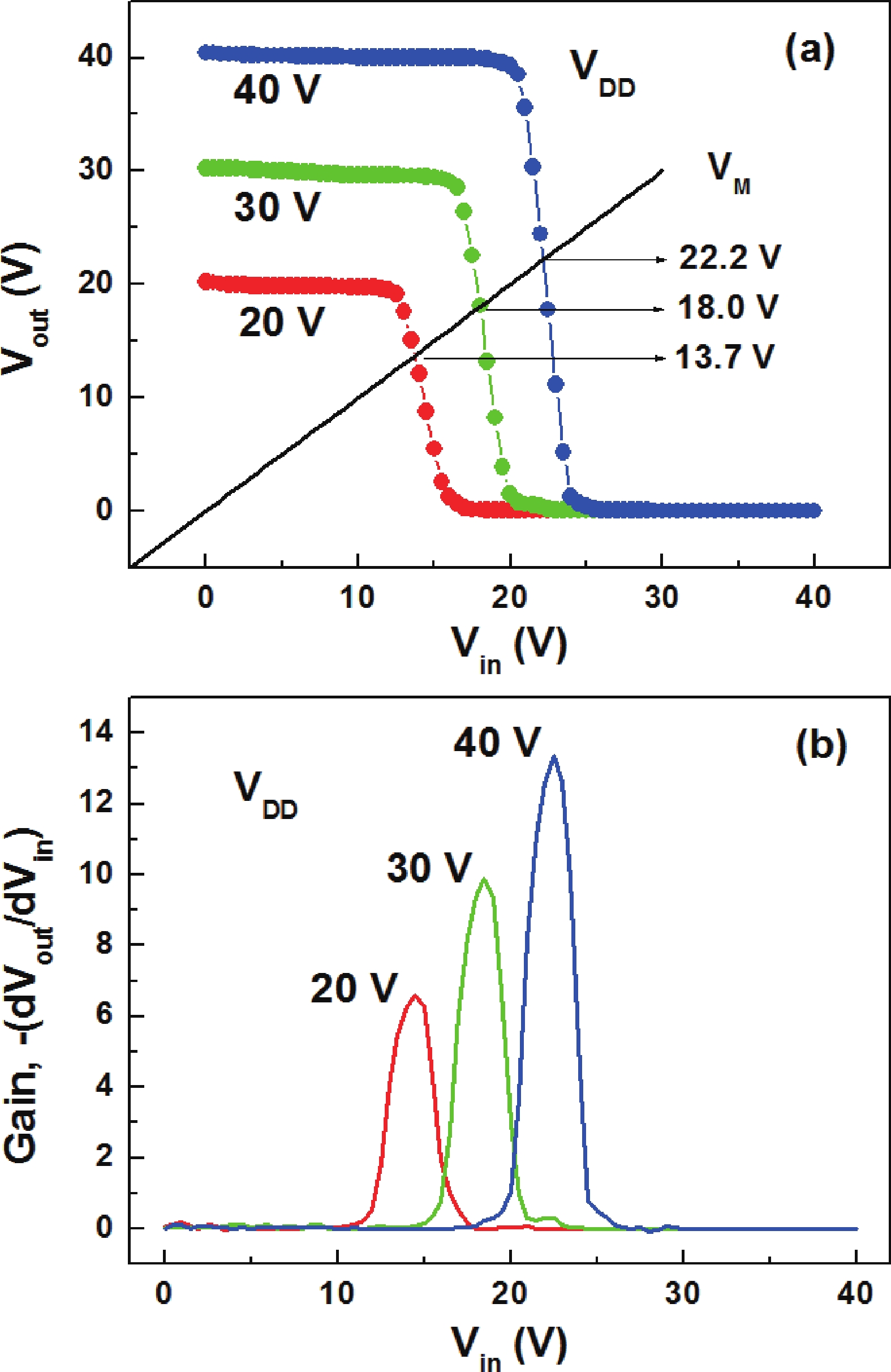
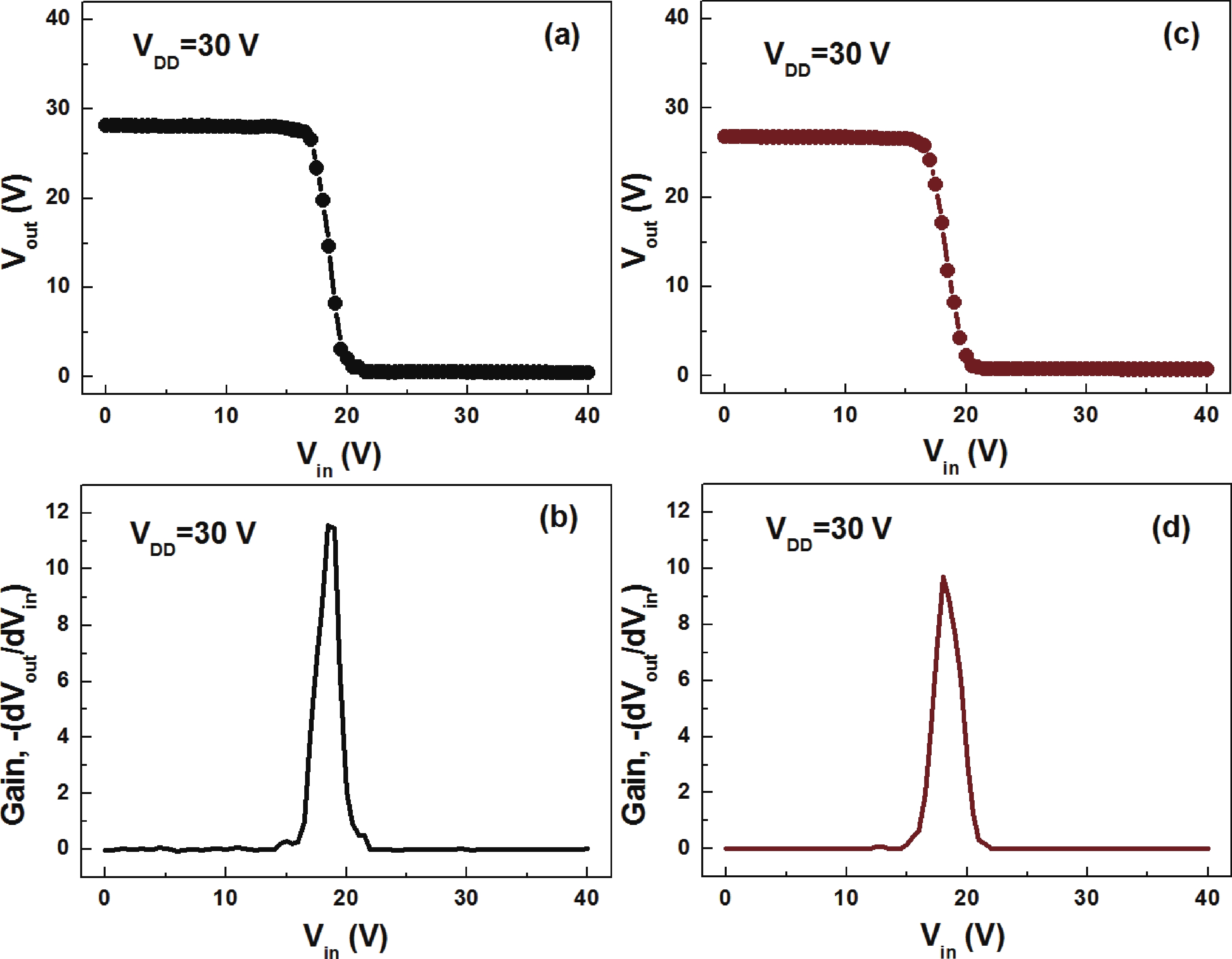
Complementary inverter is the basic unit for logic circuits, but the inverters based on full oxide thin-film transistors (TFTs) are still very limited. The next challenge is to realize complementary inverters using homogeneous oxide semiconductors. Herein, we propose the design of complementary inverter based on full ZnO TFTs. Li−N dual-doped ZnO (ZnO:(Li,N)) acts as the p-type channel and Al-doped ZnO (ZnO:Al) serves as the n-type channel for fabrication of TFTs, and then the complementary inverter is produced with p- and n-type ZnO TFTs. The homogeneous ZnO-based complementary inverter has typical voltage transfer characteristics with the voltage gain of 13.34 at the supply voltage of 40 V. This work may open the door for the development of oxide complementary inverters for logic circuits.
J. Semicond.
2025, 46(6): 062304 doi: 10.1088/1674-4926/24100017
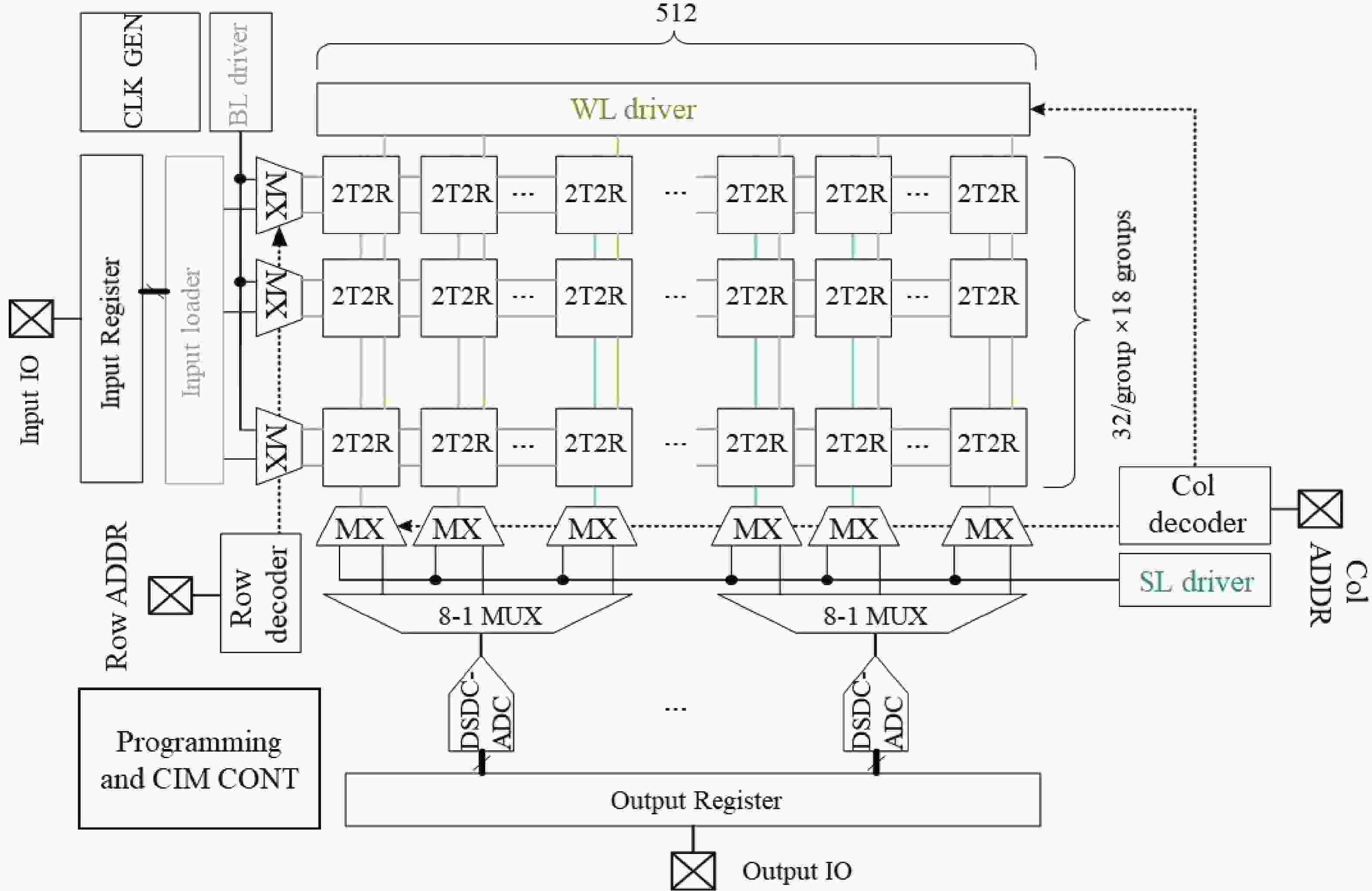
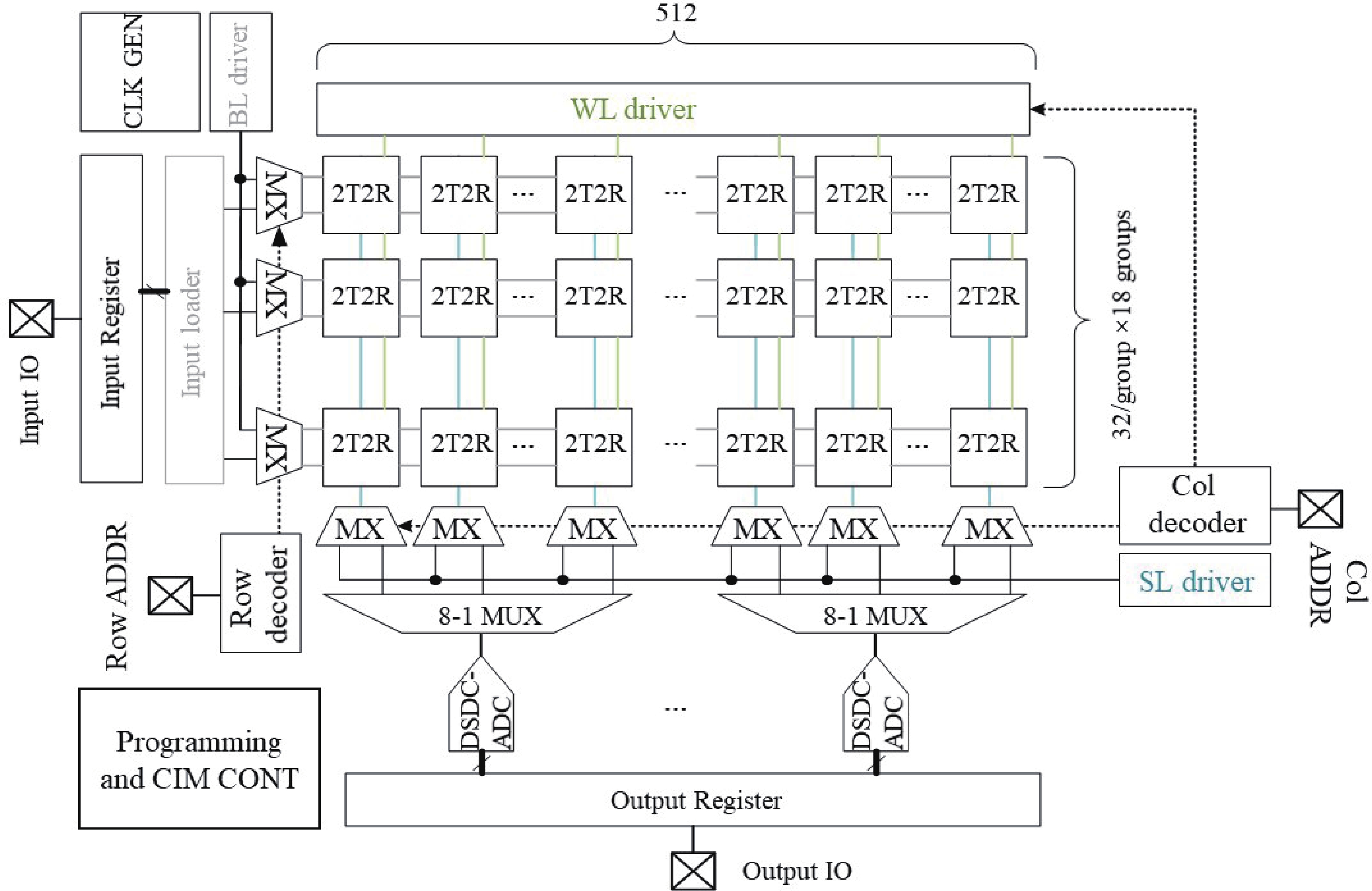
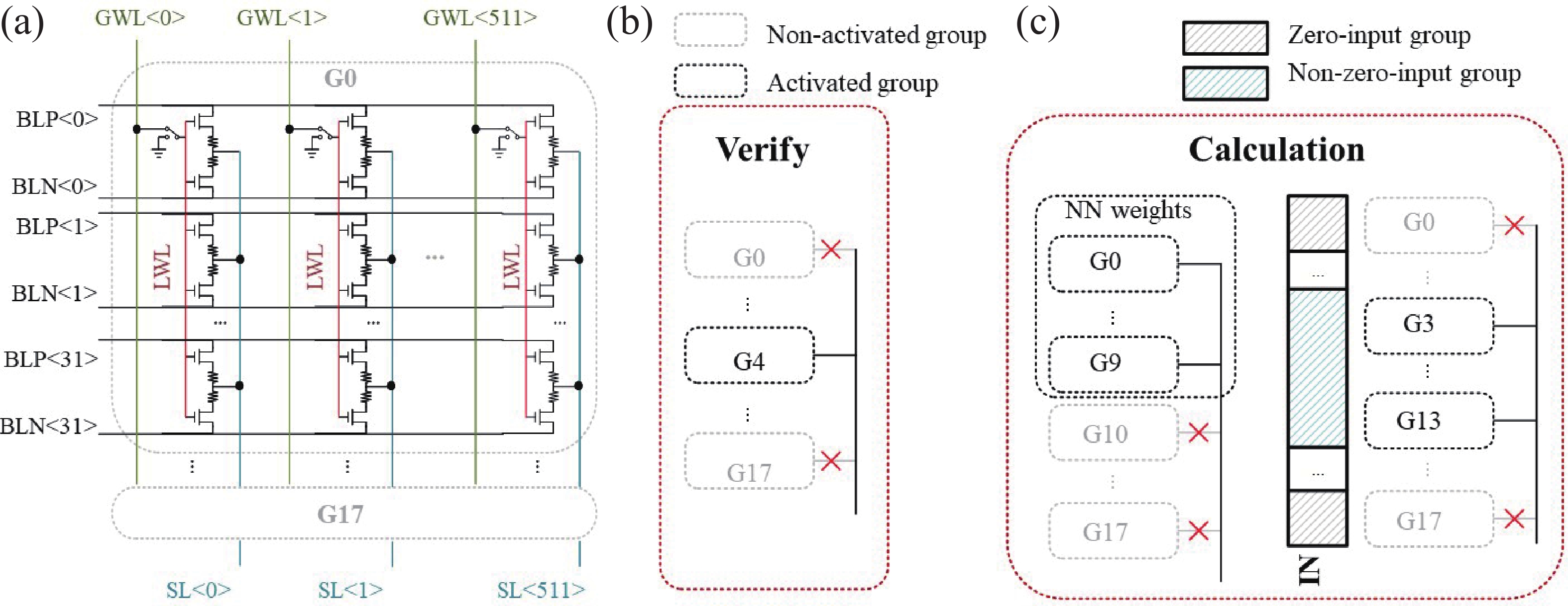
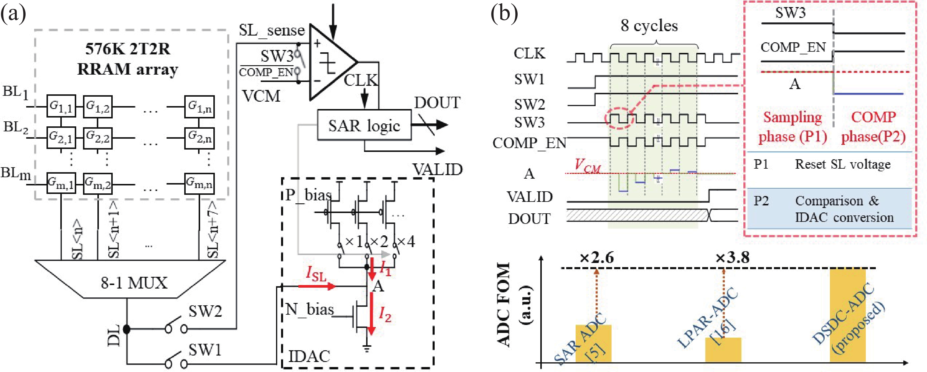
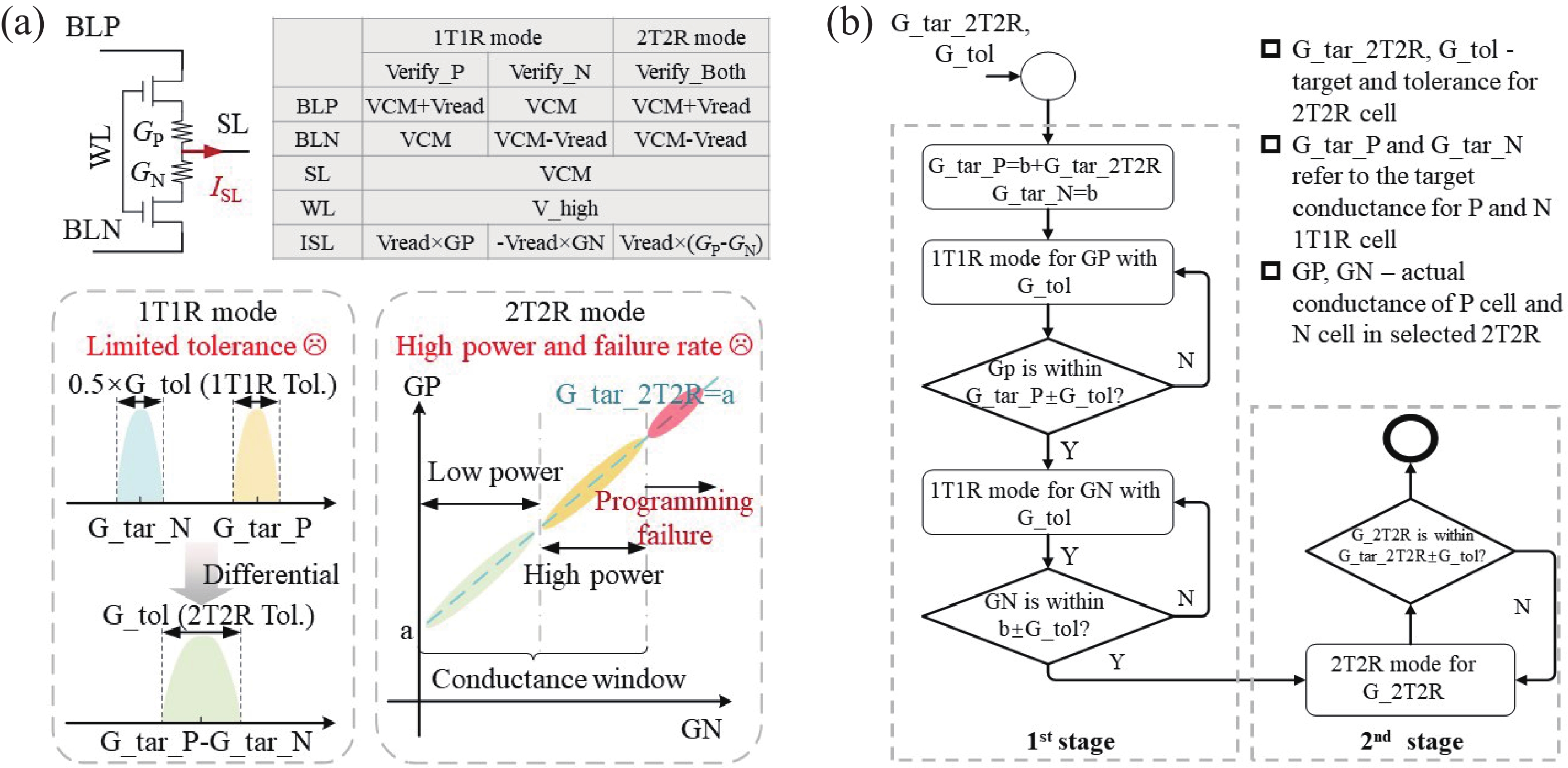
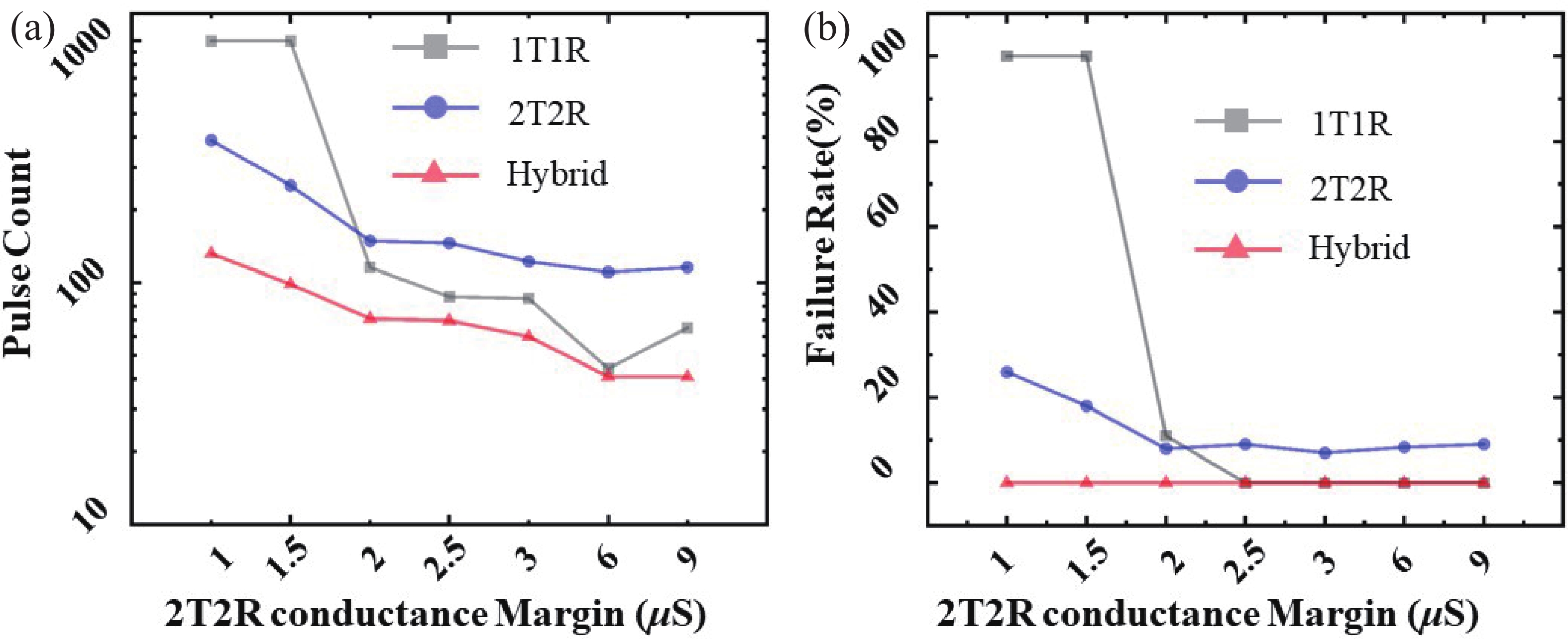
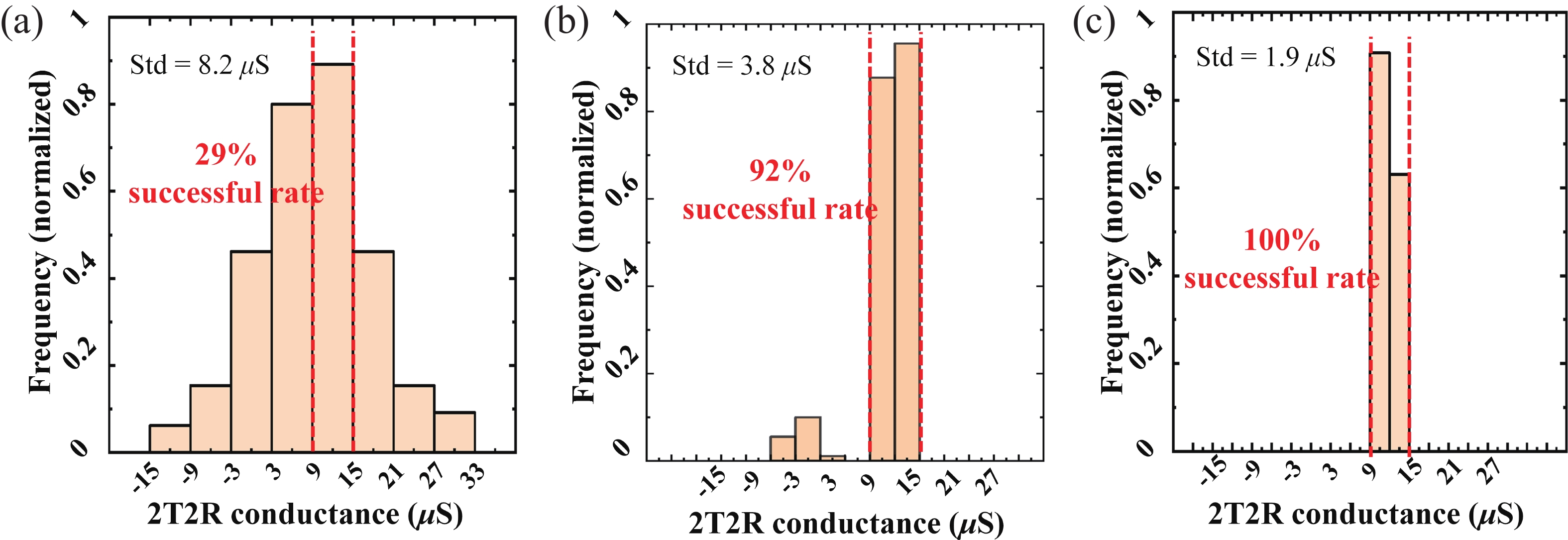
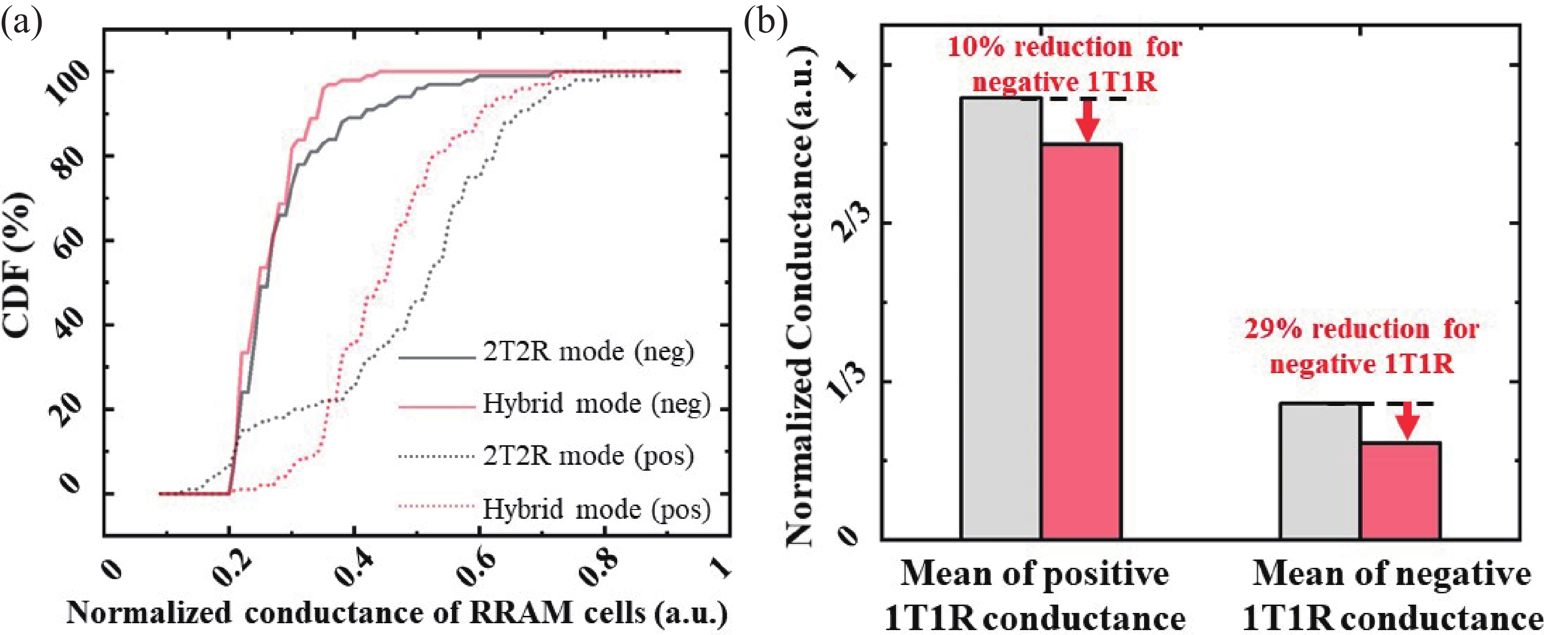
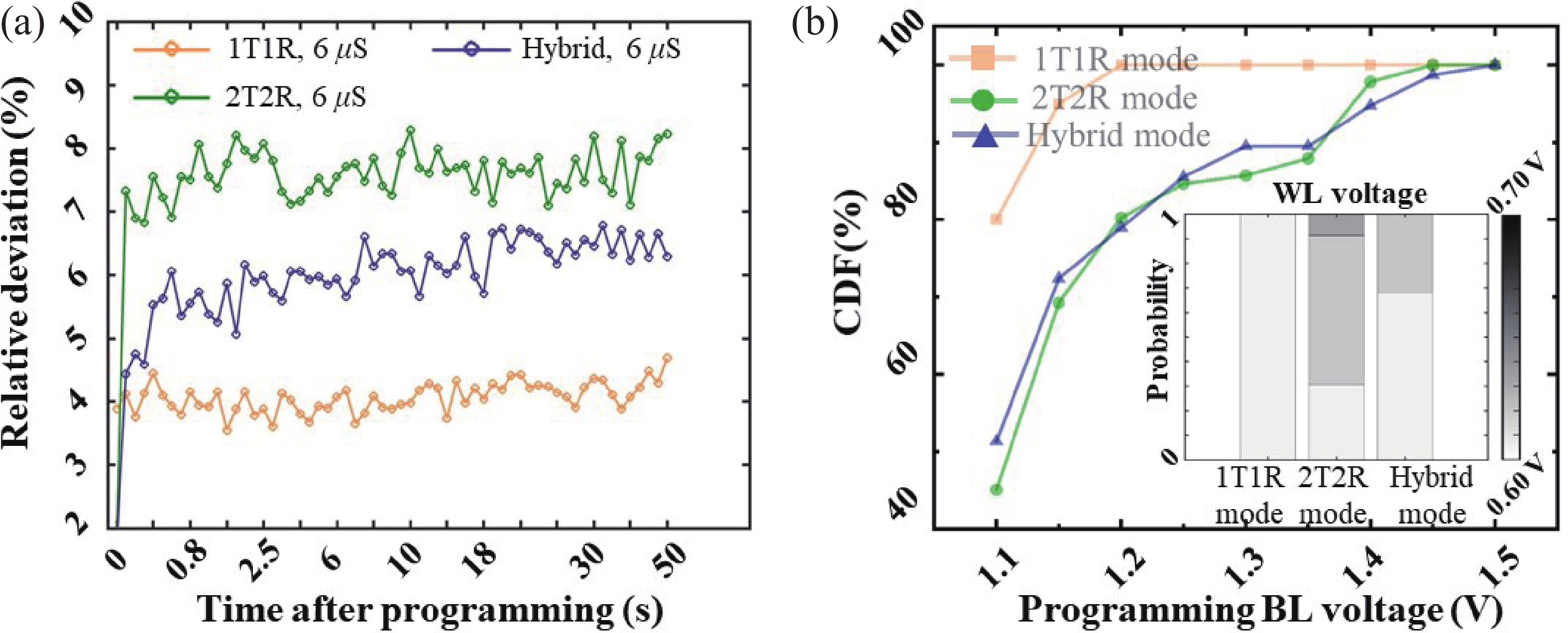
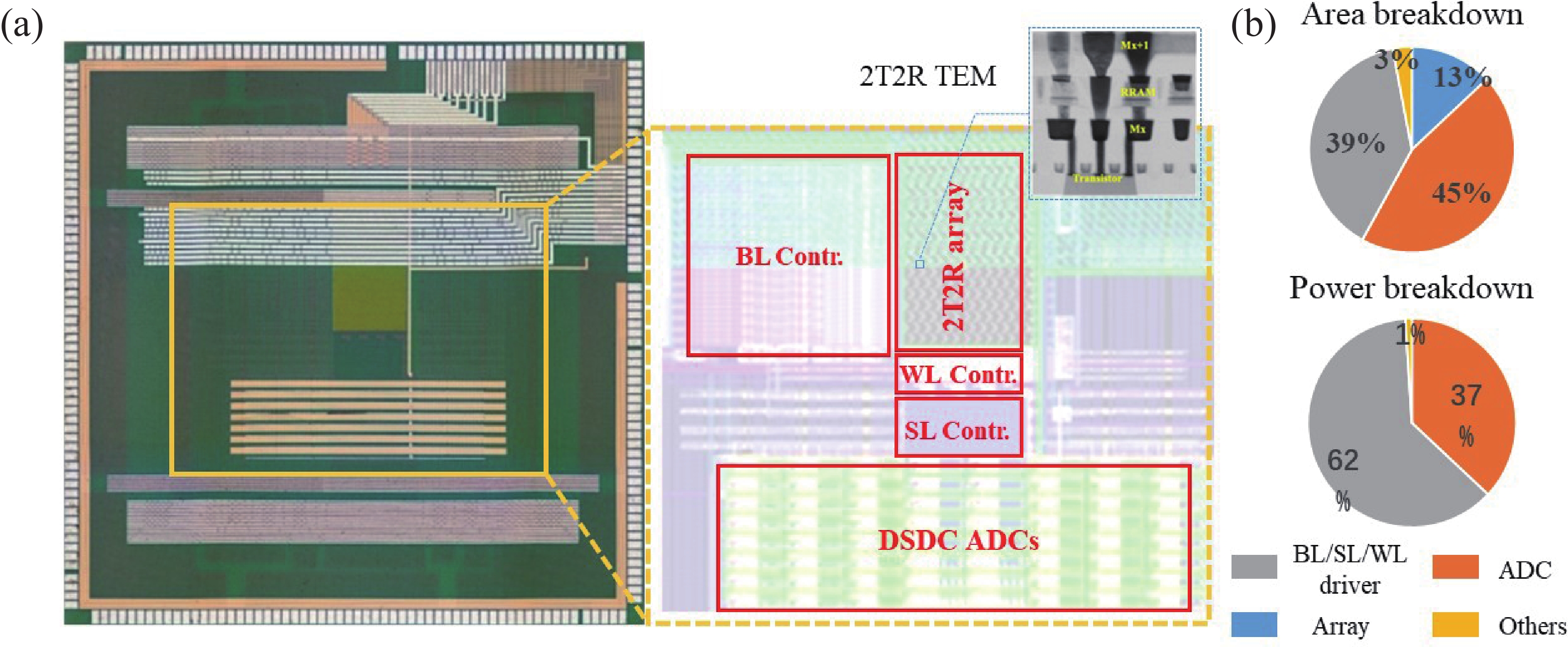
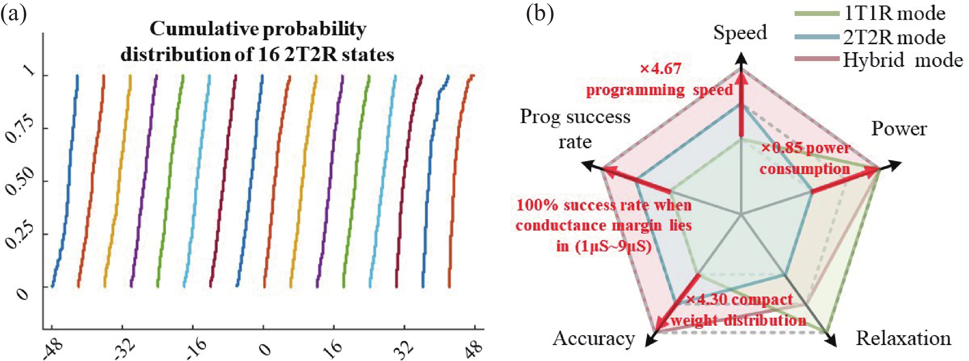
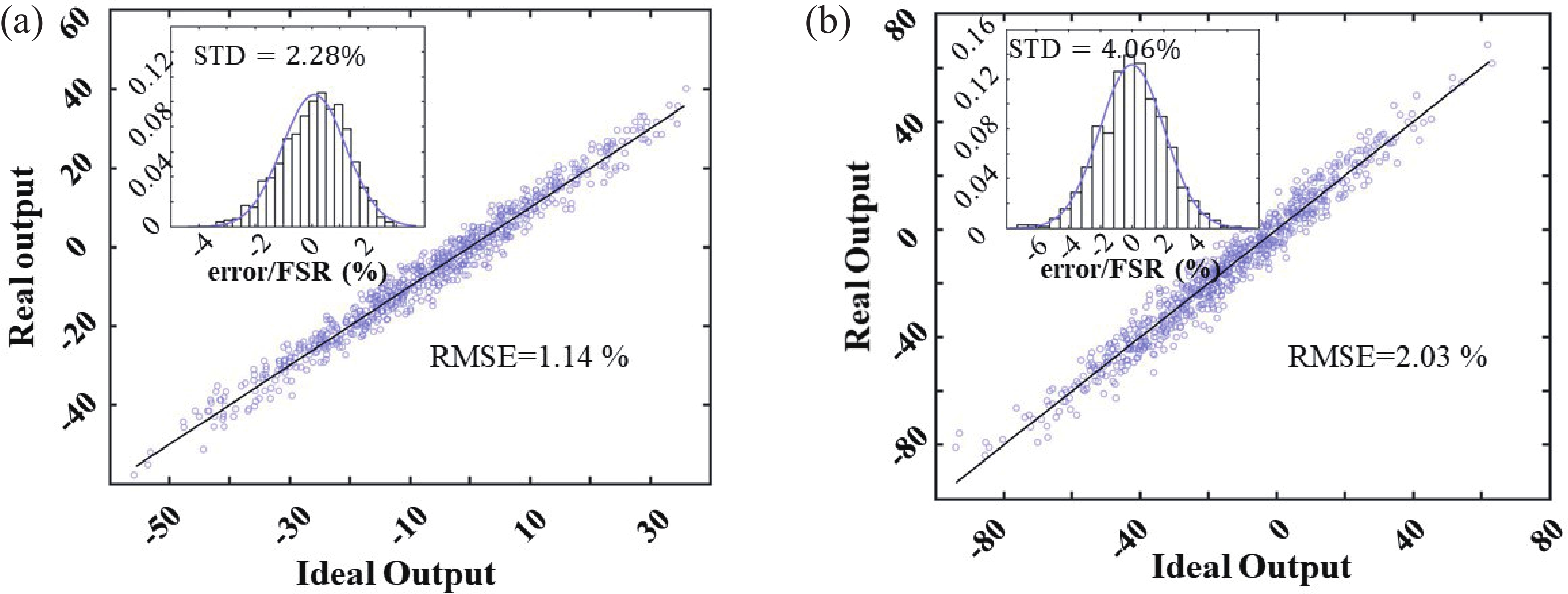
Computing-in-memory (CIM) has been a promising candidate for artificial-intelligent applications thanks to the absence of data transfer between computation and storage blocks. Resistive random access memory (RRAM) based CIM has the advantage of high computing density, non-volatility as well as high energy efficiency. However, previous CIM research has predominantly focused on realizing high energy efficiency and high area efficiency for inference, while little attention has been devoted to addressing the challenges of on-chip programming speed, power consumption, and accuracy. In this paper, a fabricated 28 nm 576K RRAM-based CIM macro featuring optimized on-chip programming schemes is proposed to address the issues mentioned above. Different strategies of mapping weights to RRAM arrays are compared, and a novel direct-current ADC design is designed for both programming and inference stages. Utilizing the optimized hybrid programming scheme, 4.67× programming speed, 0.15× power saving and 4.31× compact weight distribution are realized. Besides, this macro achieves a normalized area efficiency of 2.82 TOPS/mm2 and a normalized energy efficiency of 35.6 TOPS/W.
J. Semicond.
2025, 46(6): 062501 doi: 10.1088/1674-4926/24110029
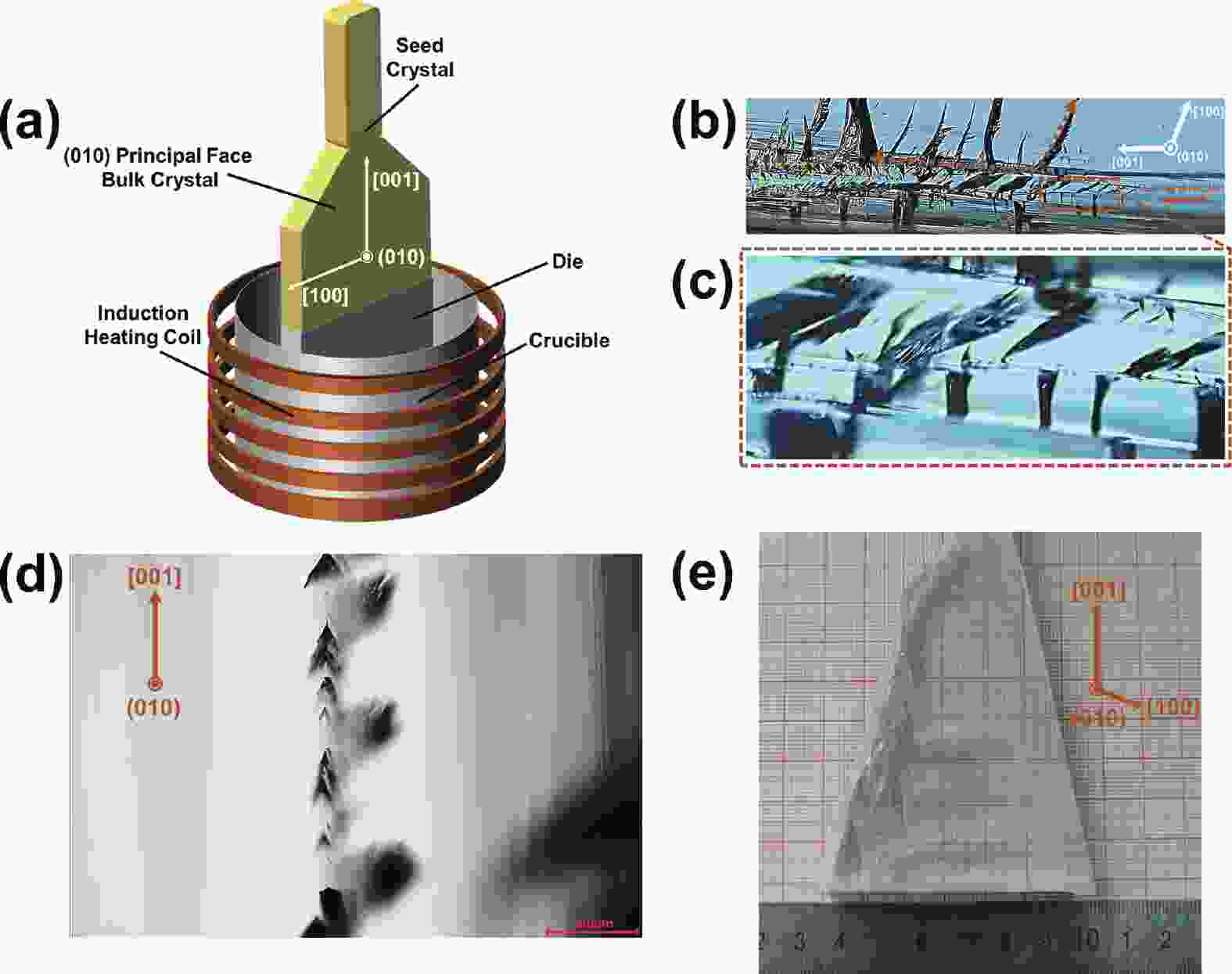
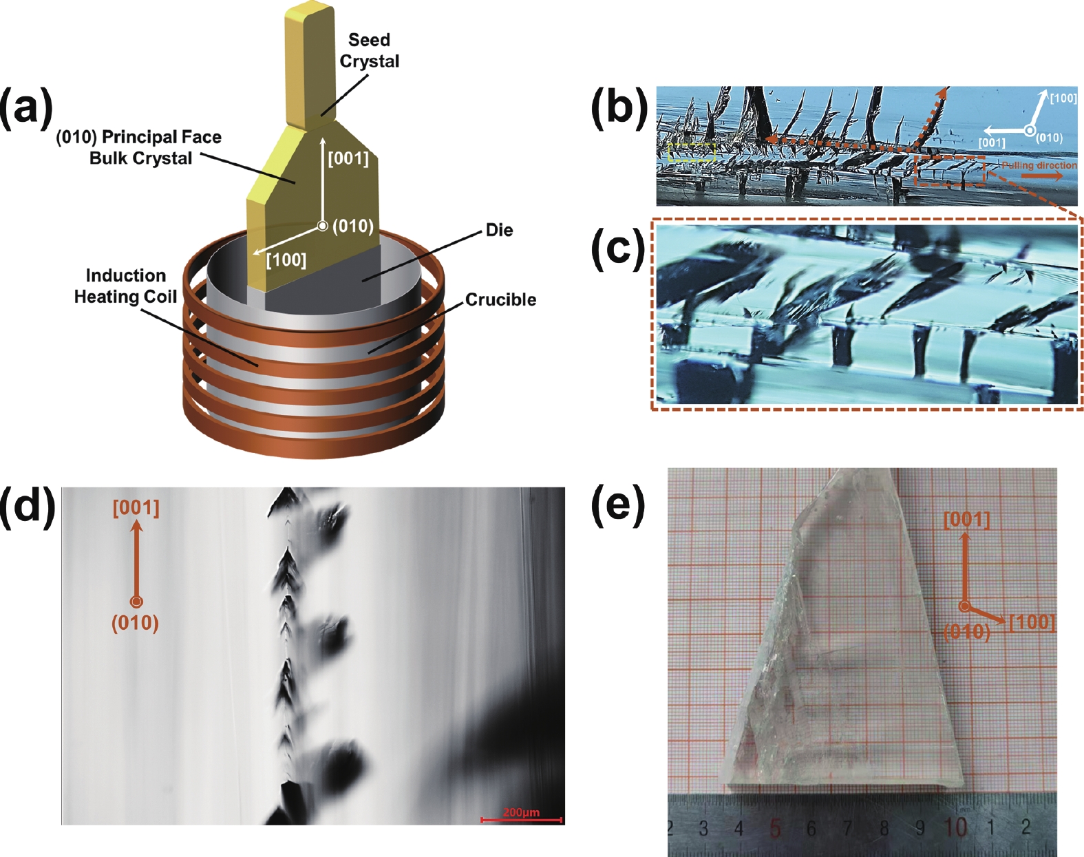
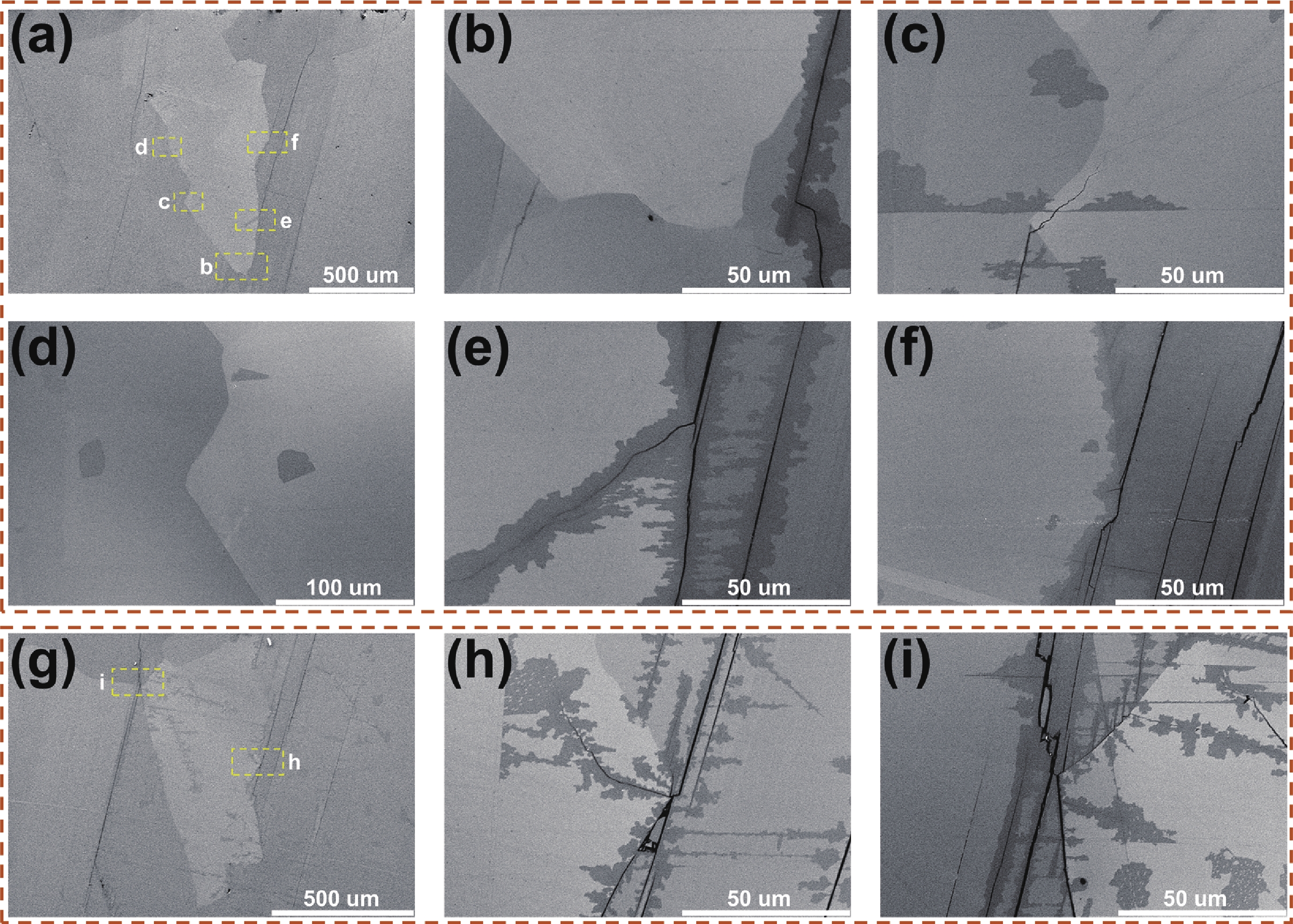
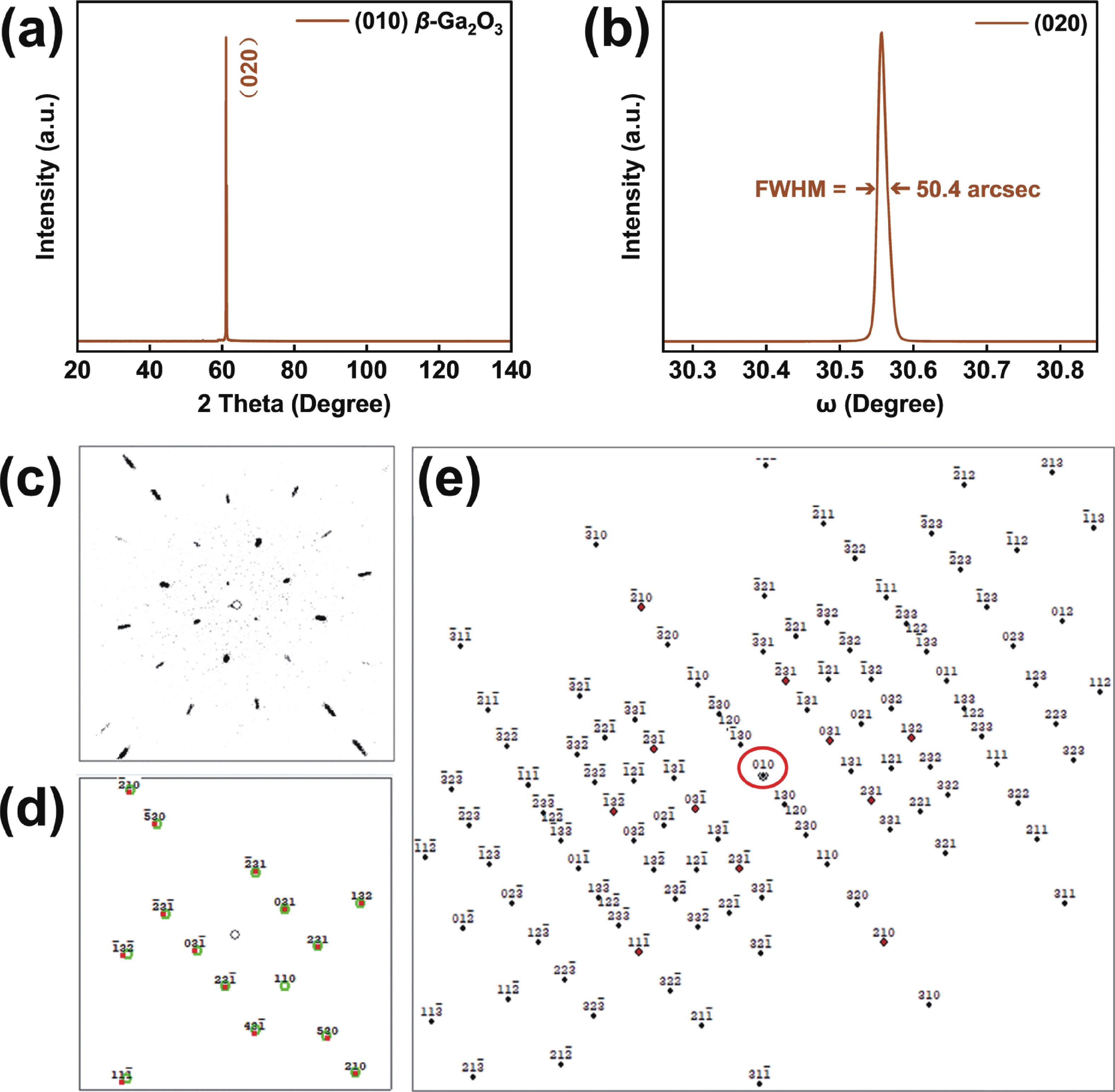
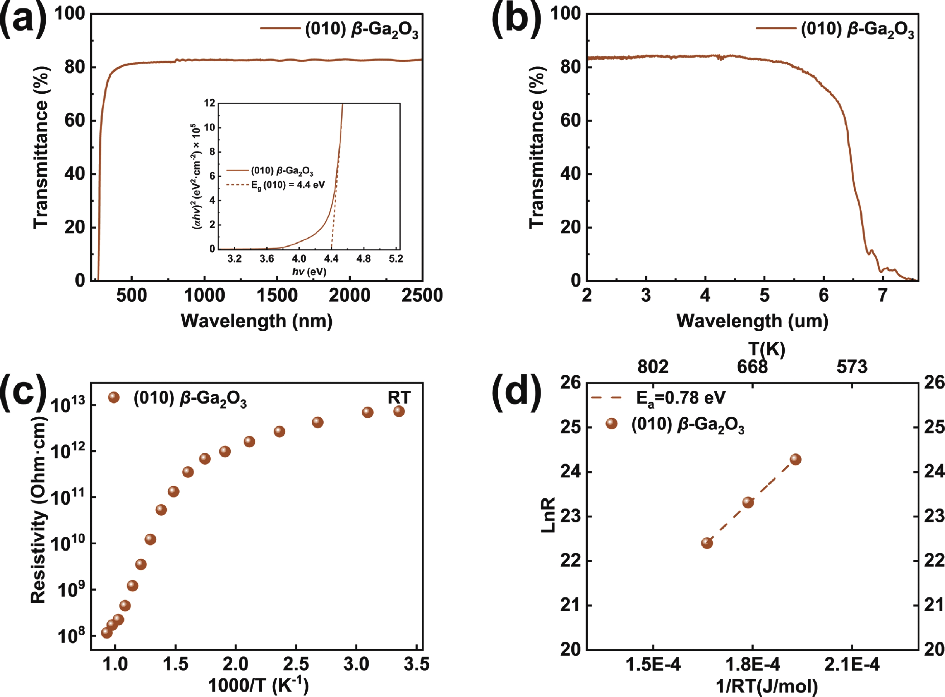
The (010)-oriented substrates of β-Ga2O3 are endowed with the maximum thermal conductivity and fastest homoepitaxial rate, which is the preferred substrate direction for high-power devices. However, the size of (010) plane wafer is critically limited by die in the commercial edge-defined film-fed growth (EFG) method. It is difficult to grow the β-Ga2O3 crystal with (010) principal face due to the (100) and (001) are cleavage planes. Here, the 2-inch diameter (010) principal-face β-Ga2O3 single crystal is successfully designed and grown by improved EFG method. Unlike previous reported techniques, the single crystals are pulled with [001] direction, and in this way the (010) wafers can be obtained from the principal face. In our experiments, tree-like defects (TLDs) in (010) principal-face bulk crystals are easy to generate. The relationship between stability of growth interface and origin of TLDs are thoroughly discussed. The TLDs are successfully eliminated by optimizing growth conditions. The high crystalline quality of (010)-oriented substrates are comprehensive demonstrated by full width at half maximum (FWHM) with 50.4 arcsec, consistent orientation arrangement of (010) plane, respectively. This work shows that the (010)-oriented substrates can be obtained by EFG method, predicting the commercial prospects of large-scale (010)-oriented β-Ga2O3 substrates.